Embed Size (px)
Citation preview
University of Pennsylvania University of Pennsylvania
ScholarlyCommons ScholarlyCommons
Departmental Papers (MSE) Department of Materials Science & Engineering
6-3-2011
In Situ Nanomechanical Testing in Focused Ion Beam and Nanomechanical Testing in Focused Ion Beam and
Scanning Electron Microscopes Scanning Electron Microscopes
Daniel S. Gianola University of Pennsylvania; Karlsruhe Institute of Technology, [email protected]
Andreas Sedlmayr Karlsruhe Institute of Technology
Reiner Mönig Karlsruhe Institute of Technology
Cynthia A. Volkert University of Göttingen
Ryan C. Major Hysitron, Inc.
See next page for additional authors
Follow this and additional works at: https://repository.upenn.edu/mse_papers
Part of the Materials Science and Engineering Commons
Recommended Citation Recommended Citation Gianola, D. S., Sedlmayr, A., Mönig, R., Volkert, C. A., Major, R. C., Cyrankowski, E., Asif, S. S., Warren, O. L., & Kraft, O. (2011). In Situ Nanomechanical Testing in Focused Ion Beam and Scanning Electron Microscopes. Retrieved from https://repository.upenn.edu/mse_papers/205
Suggested Citation: Gianola, D.S. et al.In situ nanomechanical testing in focused ion beam and scanning electron microscopes. Review of Scientific Instruments. 8282, 063901.
© 2011 American Institute of Physics. This article may be downloaded for personal use only. Any other use requires prior permission of the author and the American Institute of Physics. The following article appeared in Review of Scientific Instruments. and may be found at http://dx.doi.org/10.1063/1.3595423
This paper is posted at ScholarlyCommons. https://repository.upenn.edu/mse_papers/205 For more information, please contact [email protected].

In Situ Nanomechanical Testing in Focused Ion Beam and Scanning Electron Nanomechanical Testing in Focused Ion Beam and Scanning Electron Microscopes Microscopes
Abstract Abstract The recent interest in size-dependent deformation of micro- and nanoscale materials has paralleled both technological miniaturization and advancements in imaging and small-scale mechanical testing methods. Here we describe a quantitative in situ nanomechanical testing approach adapted to a dualbeam focused ion beam and scanning electron microscope. A transducer based on a three-plate capacitor system is used for high-fidelity force and displacement measurements. Specimen manipulation, transfer, and alignment are performed using a manipulator, independently controlled positioners, and the focused ion beam. Gripping of specimens is achieved using electron-beam assisted Pt-organic deposition. Local strain measurements are obtained using digital image correlation of electron images taken during testing. Examples showing results for tensile testing of single-crystalline metallic nanowires and compression of nanoporous Au pillars will be presented in the context of size effects on mechanical behavior and highlight some of the challenges of conducting nanomechanical testing in vacuum environments.
Disciplines Disciplines Engineering | Materials Science and Engineering
Comments Comments Suggested Citation: Gianola, D.S. et al.In situ nanomechanical testing in focused ion beam and scanning electron microscopes. Review of Scientific Instruments. 8282, 063901.
© 2011 American Institute of Physics. This article may be downloaded for personal use only. Any other use requires prior permission of the author and the American Institute of Physics. The following article appeared in Review of Scientific Instruments. and may be found at http://dx.doi.org/10.1063/1.3595423
Author(s) Author(s) Daniel S. Gianola, Andreas Sedlmayr, Reiner Mönig, Cynthia A. Volkert, Ryan C. Major, Edward Cyrankowski, S.A. Syed Asif, Oden L. Warren, and Oliver Kraft
This journal article is available at ScholarlyCommons: https://repository.upenn.edu/mse_papers/205
REVIEW OF SCIENTIFIC INSTRUMENTS 82, 063901 (2011)
In situ nanomechanical testing in focused ion beam and scanningelectron microscopes
D. S. Gianola,1,2 A. Sedlmayr,2 R. Mönig,2 C. A. Volkert,3 R. C. Major,4 E. Cyrankowski,4
S. A. S. Asif,4 O. L. Warren,4 and O. Kraft21Department of Materials Science and Engineering, University of Pennsylvania, Philadelphia, Pennsylvania19104, USA2Institute for Applied Materials, Karlsruhe Institute of Technology, Karlsruhe, Germany3Institute for Materials Physics, Georg-August University of Göttingen, Göttingen, Germany4Hysitron, Inc., Minneapolis, Minnesota 55344, USA
(Received 12 February 2011; accepted 5 May 2011; published online 3 June 2011)
The recent interest in size-dependent deformation of micro- and nanoscale materials has paralleledboth technological miniaturization and advancements in imaging and small-scale mechanical testingmethods. Here we describe a quantitative in situ nanomechanical testing approach adapted to a dual-beam focused ion beam and scanning electron microscope. A transducer based on a three-plate capac-itor system is used for high-fidelity force and displacement measurements. Specimen manipulation,transfer, and alignment are performed using a manipulator, independently controlled positioners, andthe focused ion beam. Gripping of specimens is achieved using electron-beam assisted Pt-organicdeposition. Local strain measurements are obtained using digital image correlation of electron im-ages taken during testing. Examples showing results for tensile testing of single-crystalline metallicnanowires and compression of nanoporous Au pillars will be presented in the context of size effectson mechanical behavior and highlight some of the challenges of conducting nanomechanical testingin vacuum environments. © 2011 American Institute of Physics. [doi:10.1063/1.3595423]
I. INTRODUCTION AND BACKGROUND
As technological devices continue to miniaturize and theconstituent materials that comprise them approach micro- andnanoscale dimensions, the need for accurate scale-specifictesting methods grows. The mechanical behavior of micro-and nanoscaled materials has in particular been the sub-ject of recent interest, borne from the importance of struc-tural integrity in next-generation small-scale devices, as wellas the emergence of size effects on mechanical behavior.The latter discovery has motivated a number of studies thatrevealed that the mechanical behavior of small crystals ismarkedly different than that of their bulk counterparts.1–14
These driving forces have necessitated the development ofnew techniques and testing methods that address the diffi-culties of synthesizing, handling, and measuring propertiesof micro- and nanoscaled specimens.15 Techniques rangingfrom nanoindentation,16 micro- and nanocompression,17–19
microbending,5, 11, 20–22 and micro- and nanotension8, 23–36
have been introduced using novel instrumentation and anal-ysis approaches.
In parallel, a large surge of effort has focused onin situ methodologies, where imaging and testing occursimultaneously.37 Imaging and characterization platformswith requisite spatial resolution for nanoscale investigationsthat have been employed for in situ mechanical testing in-clude scanning electron microscopy (SEM),17, 28, 36, 38–40 trans-mission electron microscopy (TEM),41–53 atomic force mi-croscopy (AFM),32, 54 micro-beam X-ray diffraction,55–57 andvisible light scattering (e.g., Raman spectroscopy).55, 58 Whilehigh-throughput in situ testing is still nascent, one advan-tage of such testing is clear; a correlation between deforma-
tion events and measurement of properties can be directly ob-tained. Despite the new approaches that have been developedto address small scale mechanical testing, not all are fullyquantitative and many result in data fraught with uncertainty.Given the technological advances in high-fidelity sensors, ac-tuators, and positioners, a strong thrust towards developing orrefining testing techniques and standardization that mitigateexperimental error and artifacts must be accomplished; thesedemands were successfully addressed for large scale mechan-ical testing (see, e.g., Ref. 59) and should be used as a guidefor small scale measurements. A comparison of several small-scale mechanical testing approaches23, 35, 60–71 is summarizedin Fig. 1, where the dynamic range in both displacement andforce measurement is highlighted.
In this work, we introduce a novel in situ nanomechanicaltesting platform consisting of a parallel-plate capacitor systemfor actuation and displacement measurement, and nanoposi-tioning stages for proper specimen alignment. The systemis capable of a wide range of nanomechanical tests, includ-ing nominally uniaxial tension and compression, nanoinden-tation, and bending. Rzepiejewska-Malyska et al. recently re-ported the development of a nanoindentation system capa-ble of being operated in an SEM environment.38 We reportthe modification and operation of a next-generation trans-ducer and extend the application to nanotensile and micro-compression testing in a dual-beam focused ion beam (FIB)and SEM instrument. Special attention is placed on meth-ods required for nanotensile specimen preparation, force-displacement transducer operating principles, vacuum com-patibility of the instrument, and the use of quantitative digitalimaging methods. We show the efficacy of this instrumenta-tion by way of two representative examples that highlight the
0034-6748/2011/82(6)/063901/12/$30.00 © 2011 American Institute of Physics82, 063901-1
Downloaded 07 Jun 2011 to 130.91.117.41. Redistribution subject to AIP license or copyright; see http://rsi.aip.org/about/rights_and_permissions

063901-2 Gianola et al. Rev. Sci. Instrum. 82, 063901 (2011)
10-10 10-9 10-8 10-7 10-6 10-5 10-4 10-3 10-210-9
10-8
10-7
10-6
10-5
10-4
10-3
10-2
10-1
100
101
Forc
era
ng
e(N
)
Displacement range (m)
Yuet al. (2000)
TanandLim(2004)
Miyazaki andHayashi (1999)
Greeket al.(1997)
Buchheit et al.(2003)
Espinosaet al. (2002)
HaqueandSaif (2001)
Orsoet al. (2006)
Richter et al. (2008)
Brenner (1960)
Sharpeet al. (1997)
20 40 60 80 100 120 14020
40
60
80
100
120
140
Displacement Dynamic Range (dB)
Forc
e D
ynam
ic R
ang
e (d
B)
limited byforce DR
limited bydisplacement DR
(a) (b)
Zhang 2000
Longtin 2004
Suwito 1999
FIG. 1. (Color online) Force versus displacement range offered by a variety of small-scale tensile testing techniques (Refs. 23 and 35, and 60–71). (a) Thelower point represents the resolution of the system, while the upper point is the maximum allowable value. (b) Force and displacement dynamic ranges of testingtechniques. We use the conventional definition of dynamic range, where DR = 20 × log(maxvalue/noisefloor), plotted in dB. The symbols correspond to thelines shown in (a) except for those labeled.
ability of these methods for interrogation of single crystal de-formation behavior at small length scales: (i) tensile testing ofsingle-crystalline metallic nanowires and (ii) microcompres-sion testing of nanoporous Au.
II. EXPERIMENTAL
A. Background of methods for in situnanomechanical testing
When the dimensions of testing specimens are decreasedto the nanoscale, there is also need for different techniques
that facilitate accurate and readily interpretable testing. Whitelight optical microscopy is no longer sufficient as the imag-ing platform at these scales due to diffraction-limited spa-tial resolution and is often replaced by electron beam imag-ing of the small specimens. Gas injection systems inside theSEM can be used for gripping the specimens in lieu of me-chanical clamps. Manipulation also needs to be done insidethe SEM and remotely, using devices that allow for fine mo-tion of the order of atomic spacing, but with large overallrange. Imaging and manipulation techniques are also crucialfor the alignment of the specimens in order to achieve nom-
(a) (b)
3-axisnano-manipulator
nanomechanicaltransducer
z-axispositionalstage
x- and y-axispositionalstages
mou
nt specimenholder
x
yz
x y
z
electronsions
Nanopositioner DOFs
Microscope stage DOFs
diamondtip
(c)force actuationcoredisplacement
sensing corecentral rod
conductive probe
FIG. 2. (Color online) Nanomechanical testing setup. (a) Image of the assembly in the vacuum chamber of the dual-beam FIB/SEM. The transducer, manipulator,and nanopositioners are arranged in a configuration that allows for sufficient range of motion and modular installation of the components. (b) Schematic of thesetup highlighting the DOF of motion available from the nanopositioning and microscope stages. Note that the nanomanipulator is not shown in (b). (c) Cross-sectional diagram of the nanomechanical transducer.
Downloaded 07 Jun 2011 to 130.91.117.41. Redistribution subject to AIP license or copyright; see http://rsi.aip.org/about/rights_and_permissions
063901-3 Gianola et al. Rev. Sci. Instrum. 82, 063901 (2011)
inally uniaxial testing conditions and allowing for facile datainterpretation.
The in situ nanomechanical testing platform reportedhere employs a FIB/SEM dual-beam system equipped witha transducer based upon a double three-plate capacitordesign,38 a nanomanipulator, and three independently con-trolled nanopositioners. A photograph and a schematic show-ing all degrees of positioning freedom are shown in Fig. 2. InSecs. II B–II D, we describe the main experimental compo-nents and approaches.
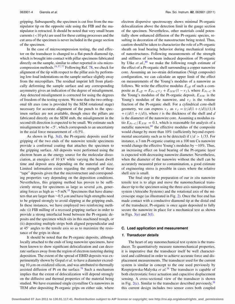
B. Nanostructure harvesting, manipulation, transfer,alignment, and gripping
The first task in performing a nanomechanical test is toidentify and isolate a single specimen. In the case of nanoin-dentation and microcompression, for instance, this involveslocating an area that has been previously prepared by stan-dard metallographic techniques or using other techniques tofabricate specimens. In the case of nanoscale tensile testing,specimens are often dispersed randomly or grown in high den-sity on a substrate, requiring careful harvesting of individualspecimens. We now focus on an example of extracting an in-dividual nanowire for subsequent tensile testing as shown inFig. 3. A standard SEM holder can be used to mount the sam-ple with synthesized nanostructures, as well as a well-definedgripping substrate. Once a specimen that meets the desired di-mensions is identified, it is aligned with the microscope stagesuch that it can be approached and gripped easily with themanipulator (Fig. 3(a)). The root of the specimen is broughtinto close proximity with the nanomanipulator tip (KleindiekNanotechnik) using a combination of stage and coarse ma-nipulator motion (Fig. 3(b)). Contact between the manipula-tor and tip can be ensured by: (i) a change in contrast due toelectrical contact, (ii) small mechanical perturbations of themanipulator, or (iii) changes in the vibration response of thespecimen due to new boundary conditions. All of these meth-ods minimize mechanical loads applied to the specimen, par-ticularly if the tip is attached at the root of a nanowire. The
specimen is then “glued” to the tip of the manipulator usinglocal electron-beam induced deposition (EBID) of a Pt-basedorganometallic precursor gas that is delivered through an in-jection system and adsorbs to nearby surfaces.72–75 Given thatthe initial attachment point is near the root of the nanowire,any mechanical deformation would occur between the tip andthe root; the free end of the wire is stress free. This point is ex-ploited for detachment of the wire from the substrate by smallmovements of the manipulator or microscope stage. Providedthat the bonding of the Pt-organic deposit is strong relativeto the substrate-wire interface, the wire will break off leav-ing a freestanding nanowire attached to the manipulator tip(Fig. 3(b)). Alternatively, the manipulator tip can be attachedat the end of the nanowire and the root can be cut free usingthe FIB. However, this method is avoided in cases where theinfluence of the ion beam is expected to have an adverse effecton mechanical response.76
Alignment of the nanowire with the first gripping sur-face must then be achieved (Fig. 3(c)). Precise alignment in-volves ensuring coincidence of the nanowire and actuationand force measurement axes, which can be challenging. Mul-tiple degrees of freedom (DOF) of stage and manipulator arerequired, as well as proper characterization of the spatial ori-entation of the specimen from its growth substrate. Giventhe difficulty of mitigating misorientation out of the imageplane, we employ an AFM cantilever as our fixed grippingsurface, which provides ample in-plane stiffness while ex-hibiting appreciable out-of-plane compliance (bending of thecantilever about its transverse axis). The efficacy of this ap-proach in eliminating misalignment issues depends on the de-gree of misalignment and the relative stiffness of the speci-men being tested. Nevertheless, the location of fracture canbe used as a gauge; fracture near the grips implies significantconcentration of stress, while fracture in the middle of thespecimen indicates good alignment. Only data from the latterevents are used when reporting tensile strength values. Bring-ing the cantilever and the free end of the specimen into alignedcontact is accomplished using the microscope stage andmanipulator. Local Pt-organic EBID is applied once more for
(a) (b) (c)LOCATE DETACH ALIGN Sicantilever
10 µm 10 µm
10 µm
(d) ATTACH / GRIP
Pt-C
nanowire
500 nm
(f)
Sicantilever
nanomechancicaltransducer
100 µm
(e)
TEST
5 µm
FIG. 3. SEM images showing the steps required to harvest quasi-1D nanostructures for mechanical testing. The sequence of manipulation, transfer, alignment,gripping, and tensile testing of nanowire specimen is shown. (f) A low-magnification image of the testing configuration showing the diamond tip attached to thetransducer (bottom) as well as the fixed grip (top). The nanowire specimen is barely visible in the center of the image.
Downloaded 07 Jun 2011 to 130.91.117.41. Redistribution subject to AIP license or copyright; see http://rsi.aip.org/about/rights_and_permissions
063901-4 Gianola et al. Rev. Sci. Instrum. 82, 063901 (2011)
gripping. Subsequently, the specimen is cut free from the ma-nipulator tip on the opposite side using the FIB and the ma-nipulator is retracted. It should be noted that very small beamcurrents (<10 pA) are used for these cutting processes and thecut area of the specimen is never included in the gauge sectionof the specimen.
In the case of microcompression testing, the end effec-tor on the transducer is changed to a flat-punch diamond tip,which is brought into contact with pillar specimens fabricateddirectly on the sample, similar to other reported in situ micro-compression methods.19, 57, 77 Following Ref. 78, we check foralignment of the tip with respect to the pillar axis by perform-ing low-load indentations on the sample surface slightly awayfrom the micropillars. The residual imprint left from plasti-cally deforming the sample surface and any correspondingasymmetry gives an indication of the degree of misalignment.Any detected misalignment is corrected for using the degreesof freedom of the testing system. We note that the two orthog-onal tilt axes (one is provided by the SEM rotational stage)necessary for accurate alignment of the punch to the spec-imen surface are not available, though since the pillars arefabricated directly on the SEM stub, the misalignment in thesecond tilt direction is expected to be small. We estimate suchmisalignment to be <5◦, which corresponds to an uncertaintyin the axial force measurement of <0.5%.
As shown in Fig. 3(d), the Pt-organic deposits used forgripping of the two ends of the nanowire tensile specimensprovide a conformal coating that attaches the specimen tothe gripping surface. All deposits were performed using theelectron beam as the energy source for the molecular disso-ciation, at energies of 10 kV while varying the beam dwelltime and deposit area depending on the material and size.Limited information exists regarding the strength of these“tape” deposits given that the microstructure and correspond-ing properties vary depending on the deposition conditions.Nevertheless, this gripping method has proven to be suffi-ciently strong for specimens as large as several μm, gener-ating forces as high as ∼5 mN.35 Specimens that have diame-ters that are larger than ∼0.5 μm and have high strengths needto be gripped strongly to avoid slipping at the gripping ends.In these instances, we have employed two reinforcing meth-ods: (i) FIB milling of a recessed gripping surface in order toprovide a strong interfacial bond between the Pt-organic de-posits and the specimen which sits in this machined trough, or(ii) depositing multiple strips both aligned perpendicular andat 45◦ angles to the tensile axis so as to maximize the resis-tance of the grips in shear.
It should be noted that the Pt-organic deposits, althoughlocally attached to the ends of long nanowire specimens, havebeen known to show significant delocalization and can deco-rate surfaces away from the region of electron rastering duringdeposition. The extent of the spread of EBID deposits was ex-perimentally shown by Gopal et al. to have a diameter exceed-ing 10 μm on oxidized silicon, and was attributed to thermallyassisted diffusion of Pt on the surface.79 Such a mechanismimplies that the extent of delocalization will depend stronglyon the diffusive and thermal properties of the material beingstudied. We have examined single crystalline Cu nanowires inTEM after depositing Pt-organic grips on either side, where
electron dispersive spectroscopy shows minimal Pt-organicdelocalization above the detection limit in the gauge sectionof the specimen. Nevertheless, other materials could poten-tially show enhanced diffusion of the Pt-organic species, re-sulting in decoration of the nanostructure being tested. Thus,caution should be taken to characterize the role of a Pt-organicsheath on load bearing behavior during mechanical testingof nanostructures. Following measurements of the strengthand stiffness of ion-beam induced deposition of Pt-organicby Utke et al.,80 we make the following rough estimate ofthe effect of a Pt-organic shell surrounding a copper nanowirecore. Assuming an iso-strain deformation (Voigt composite)configuration, we can calculate an upper limit of the effecton measurements of the Young’s modulus of a nanowire asfollows. We write the effective modulus Eeff of such a com-posite as Eeff = EPt−C v f + ENW (1 − v f ), where EPt−C isthe Young’s modulus of the Pt-organic deposit, ENW is theYoung’s modulus of the nanowire, and v f is the volumefraction of the Pt-organic shell. For a cylindrical core-shellgeometry, we can express v f as v f = (t/d(1 + t/d))/(1/4+ t/d(1 + t/d)), where t is the thickness of the shell and dis the diameter of the nanowire core. Assuming a modulus ra-tio EPt−C/ENW = 0.1, which is reasonable for analysis of ametallic nanowire,80 the effective modulus of the compositewould change by more than 10% (sufficiently beyond experi-mental uncertainty such as to be detected) if t/d > 1/33. Forinstance, a 3 nm Pt-organic coating on a 100 nm Cu nanowirewould change the effective Young’s modulus by ∼10%. Thus,an increasing effect on load bearing of the Pt-organic layeris expected with decreasing nanowire diameter. Nevertheless,when the diameter of the nanowire without the shell can beaccurately measured prior to contamination, a good estimateof engineering stress is possible in cases where the relativeshell size is small.
The final step in the preparation of our in situ nanowiretensile test is to align and move the nanomechanical trans-ducer tip to the specimen using the three-axis nanopositioningsystem (Attocube Systems) and the rotational axis of the mi-croscope stage (as illustrated in Fig. 2). Once the free end hasmade contact with a conductive diamond tip at the distal endof the transducer, Pt-organic is once again deposited to fullysecure the nanowire in place for a mechanical test as shownin Figs. 3(e) and 3(f).
C. Load application and measurement
1. Transducer details
The heart of any nanomechanical test system is the trans-ducer. To quantitatively measure nanomechanical properties,it is imperative that the transducer itself be well character-ized and calibrated in order to achieve accurate force and dis-placement measurements. The transducer used for the currentsystem is similar in concept to the one used previously byRzepiejewska-Malyska et al.38 The transducer is capable ofboth electrostatic force actuation and capacitive displacementsensing. A cross-sectional view of the transducer is shownin Fig. 2(c). Similar to the transducer described previously,38
this current design includes two sensor cores both coupled
Downloaded 07 Jun 2011 to 130.91.117.41. Redistribution subject to AIP license or copyright; see http://rsi.aip.org/about/rights_and_permissions
063901-5 Gianola et al. Rev. Sci. Instrum. 82, 063901 (2011)
(a) (b)
(c)
HV Drive B = 0 V
HV Drive A = 0 V
SynchronousDemodulator
Ampli er
DC Output = 0 Vd1 = d2
d1d2
Rest Position (Theoretical)
DC Output < 0 Vd1<d2
HV Drive A ActivatedIndentation/Compression Mode
DC Output > 0 Vd1>d2
HV Drive B ActivatedTensile Mode
DisplacementSensing
Core
ActuationCore
Central Rod(isolated from center plates)
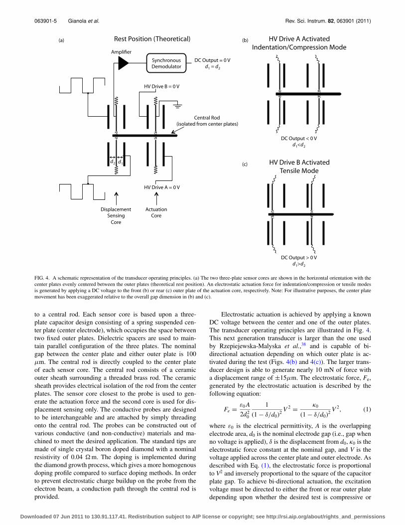
FIG. 4. A schematic representation of the transducer operating principles. (a) The two three-plate sensor cores are shown in the horizontal orientation with thecenter plates evenly centered between the outer plates (theoretical rest position). An electrostatic actuation force for indentation/compression or tensile modesis generated by applying a DC voltage to the front (b) or rear (c) outer plate of the actuation core, respectively. Note: For illustrative purposes, the center platemovement has been exaggerated relative to the overall gap dimension in (b) and (c).
to a central rod. Each sensor core is based upon a three-plate capacitor design consisting of a spring suspended cen-ter plate (center electrode), which occupies the space betweentwo fixed outer plates. Dielectric spacers are used to main-tain parallel configuration of the three plates. The nominalgap between the center plate and either outer plate is 100μm. The central rod is directly coupled to the center plateof each sensor core. The central rod consists of a ceramicouter sheath surrounding a threaded brass rod. The ceramicsheath provides electrical isolation of the rod from the centerplates. The sensor core closest to the probe is used to gen-erate the actuation force and the second core is used for dis-placement sensing only. The conductive probes are designedto be interchangeable and are attached by simply threadingonto the central rod. The probes can be constructed out ofvarious conductive (and non-conductive) materials and ma-chined to meet the desired application. The standard tips aremade of single crystal boron doped diamond with a nominalresistivity of 0.04 � m. The doping is implemented duringthe diamond growth process, which gives a more homogenousdoping profile compared to surface doping methods. In orderto prevent electrostatic charge buildup on the probe from theelectron beam, a conduction path through the central rod isprovided.
Electrostatic actuation is achieved by applying a knownDC voltage between the center and one of the outer plates.The transducer operating principles are illustrated in Fig. 4.This next generation transducer is larger than the one usedby Rzepiejewska-Malyska et al.,38 and is capable of bi-directional actuation depending on which outer plate is ac-tivated during the test (Figs. 4(b) and 4(c)). The larger trans-ducer design is able to generate nearly 10 mN of force witha displacement range of ±15μm. The electrostatic force, Fe,generated by the electrostatic actuation is described by thefollowing equation:
Fe = ε0 A
2d20
1
(1 − δ/d0)2 V 2 = κ0
(1 − δ/d0)2 V 2, (1)
where ε0 is the electrical permittivity, A is the overlappingelectrode area, d0 is the nominal electrode gap (i.e., gap whenno voltage is applied), δ is the displacement from d0, κ0 is theelectrostatic force constant at the nominal gap, and V is thevoltage applied across the center plate and outer electrode. Asdescribed with Eq. (1), the electrostatic force is proportionalto V2 and inversely proportional to the square of the capacitorplate gap. To achieve bi-directional actuation, the excitationvoltage must be directed to either the front or rear outer platedepending upon whether the desired test is compressive or
Downloaded 07 Jun 2011 to 130.91.117.41. Redistribution subject to AIP license or copyright; see http://rsi.aip.org/about/rights_and_permissions
063901-6 Gianola et al. Rev. Sci. Instrum. 82, 063901 (2011)
tensile, respectively (see Figs. 4(b) and 4(c)). During the test,the gap between the center and outer electrodes will changewhich will in turn result in a change to the electrostatic force.Equation (1) takes into account this change in electrode gap.
To detect displacements, a ratiometric method is used in-volving a high frequency (∼125 kHz square wave) signal onone of the fixed outer plates and a second signal of the samefrequency but phase shifted by 180◦ on the other outer plate.The high frequency signal is much higher than the mechanicalbandwidth of the transducer (∼100 Hz) and, consequently, thehigh frequency voltages applied for the sensing do not actuatethe transducer. In the three-plate capacitor design, each outerplate and center plate combination can be considered as a sep-arate capacitor (with capacitances C1 and C2). As the centerplate moves, a high impedance pre-amplifier circuit is used tomeasure the change in capacitance. The pre-amplifier circuitis designed to produce a DC voltage output proportional to thedisplacement. In the absence of stray capacitance, the voltageoutput Vout from the sensor is proportional to the capacitanceratio as described with the following equation:
Vout ∝ C2 − C1
C1 + C2, (2)
where C1 and C2 are the two capacitances in the differentialcapacitance sensing.
In order to minimize pump down time, only high vacuumor ultra-high vacuum compatible materials were incorporatedinto the design. Components containing magnetic impuritieswere also avoided to prevent interference with the electronbeam and/or electron imaging.
2. Calibration
The displacement calibration is done over a range of±15 μm with the transducer mounted horizontally, which isthe typical operational orientation for compression/tensile testmodes. In this orientation, the voltage output of the transducerwas determined to be linear with a linearity error of <1% overthis range. Calibration of the spring stiffness of the transducer(k = 362 N/m) involves using certified deadweights and laserinterferometry with the transducer mounted in a vertical ori-entation. In this position, the center plate is offset by ∼20 μmrelative to the horizontal rest position. Finite element analy-sis of the transducer design indicated that the spring stiffnessshould be constant over displacements of at least ±25 μmabout the relaxed state of the horizontal configuration. There-fore, the measured spring stiffness in the vertical orientationshould be valid for the horizontal orientation. Before testingand at regular intervals, the zero-volt electrostatic force con-stant, κ0, and the zero-volt rest gap d0, are determined from alarge displacement actuation with the tip out of sample con-tact (see Eq. (1)). During this test the electrostatic force gener-ated, Fe, must be equal to kδ based upon a linear spring model.This out-of-contact calibration is integrated into the software,which makes the task relatively quick and routine. The linear-ity error of the out-of-contact force-displacement curve (andthus the spring constant) was determined to be <1% over thecalibrated range of the transducer. The force calibration wasalso verified by testing with a reference transducer as well
indenting against a flexure device of known spring constant.The displacement calibration was verified by both a referencetransducer as well as SEM observation. Each actuation direc-tion requires its own displacement and electrostatic force cal-ibration.
For certain tests the transducer and sample may be tiltedwith respect to the electron beam in order to better view thecontact zone during the test. The maximum possible tilt isabout 30◦ for this system. At higher tilt angles there is therisk of collision between the transducer housing and the elec-tron column. The maximum tilt angle will vary based uponSEM manufacturer, chamber design, and orientation of thenanomechanical test instrument relative to the tilt axis of theSEM. Also, the number and placement of auxiliary com-ponents (e.g., detectors, manipulators, gas injection needles,etc.) on the chamber may restrict movement. As the trans-ducer is tilted, the weight of the center plate/central rod as-sembly causes a “forward” displacement shift. The calibratedrange of ±15 μm is referenced to the relaxed state of the hor-izontal configuration. For a tilt angle of 30◦, the center platewill be offset by ∼10 μm. In order to stay within the cal-ibrated working range of the transducer, the maximum dis-placement in the forward direction will be reduced by the off-set. This travel range is restricted by software control. Theelectrostatic force calibration routine should also be repeatedif the orientation of the transducer changes (e.g., transducertilted). Improved calibration methods are currently being ex-plored to increase the calibrated range of travel.
3. Control system and feedback operation
A recently developed digital signal processor (DSP)based controller and data acquisition system (performechTM,Hysitron, Inc.) was utilized for nanomechanical test control.The controller interfaces to a PC through a USB 2.0 link. Thecontroller includes 24-bit ADCs and 16-bit DACs for analogsignal acquisition and analog output, respectively. The DSParchitecture is ideally suited for the calculation of intensivealgorithms implemented for the various transducer controland test modes. There are three basic control modes used tooperate the transducer, which include open-loop load ramp,closed-loop displacement control with displacement set pointramp and true closed-loop load control.81 The control modescan be used to operate the transducer in either direction de-pending upon whether the desired test is tensile or indenta-tion/compression related. Prior to the test, the user definesa load or displacement versus time function, which is thentransferred to the DSP controller. Once the test is initiated,the DSP controller implements the necessary feedback algo-rithms and performs all calculations required for real-timecontrol. The internal loop cycle runs at 79 kHz, and the con-troller handles additional signal processing (e.g., data averag-ing, filtering, etc.) within the loop cycle.
4. Noise in in situ systems
For accurate results in nanomechanical testing, the pres-ence of noise in the system should be minimized. The
Downloaded 07 Jun 2011 to 130.91.117.41. Redistribution subject to AIP license or copyright; see http://rsi.aip.org/about/rights_and_permissions
063901-7 Gianola et al. Rev. Sci. Instrum. 82, 063901 (2011)
0 2 4 6 8 10
-4
-2
0
2
4
Dis
pla
cem
ent(
nm)
Time (s)
F SD = 0.06 µNd SD = 0.18 nm
0 2 4 6 8 10
-4
-2
0
2
4
Dis
pla
cem
ent(
nm)
Time (s)0 2 4 6 8 10
-4
-2
0
2
4
Dis
pla
cem
ent(
nm)
Time (s)
0 100 200 300 400 500
0.0
0.2
0.4
0.6
0.8
1.0
Nor
mal
ized
Am
plit
ude
Frequency (Hz)0 100 200 300 400 500
0.0
0.2
0.4
0.6
0.8
1.0
Nor
mal
ized
Am
plit
ude
Frequency (Hz)0 100 200 300 400 500
0.0
0.2
0.4
0.6
0.8
1.0
Nor
mal
ized
Am
pli t
ude
Frequency (Hz)
F SD = 0.46 µNd SD = 1.54 nm
F SD = 0.24 µNd SD = 0.74nm
(a) (b) (c)
(d) (e) (f )
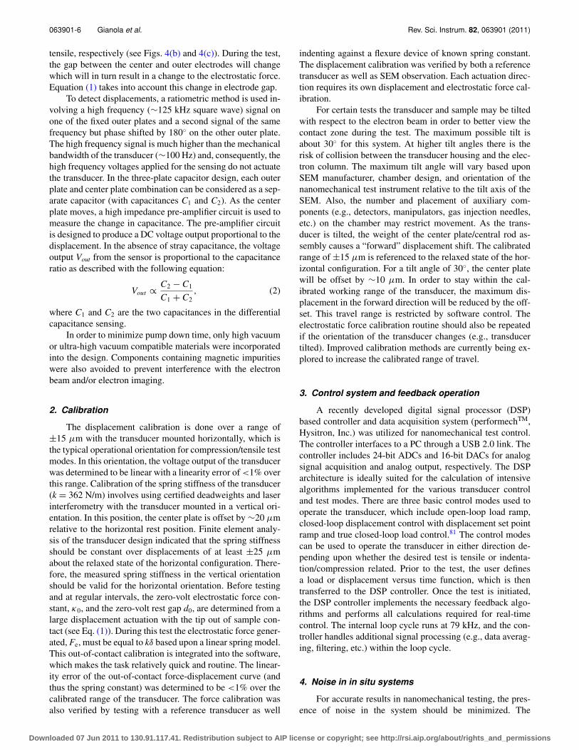
FIG. 5. Noise characteristics in air and in vacuum, revealing the different noise floors for open-loop mode in air (a), in vacuum (b), and for Q-control enabledmode in vacuum (c). The corresponding frequency response (d, e, and f) shows significant amplitude differences in mechanical resonance, which is ∼100 Hzfor the transducer assembly. The force and displacement noise floors for the different configurations are included.
occurrence of noise in a raw output signal can have manyorigins, particularly, in vacuum environments, such as:(i) mechanical vibrations, (ii) electrical noise from the ac linesource (with characteristic frequencies), and (iii) electricalnoise from stray electromagnetic fields. Strategies for elim-inating the presence of these deleterious effects can be gener-ally characterized as those preventing the origin of the noiseor those that actively compensate.
To reduce the noise and hence improve the performanceof the system, the mechanical design of the system shouldbe optimized to reduce the transfer of external noise tothe system. Two main aspects have to be considered here:(i) the mechanical connection between the microscope me-chanical stage and transducer should be as stiff as possible and(ii) the entire system should be isolated from external vi-brations. The latter is fulfilled by the pneumatic isolation ofthe microscope chamber from the ground. Besides mechani-cal measures, suitable algorithms implemented in the controlhardware and software of the transducer are used to dampenout a significant part of the noise that is caused by mechanicalresonance.
The nanomechanical transducer is designed for operationin both ambient and high vacuum environments. In a high vac-uum/low air damping environment, there is an increase in themechanical amplification at the resonance frequency and anincrease in the overall settling time of the transducer. Figure 5shows the differences of the system if operated in air or vac-uum. The time domain in Fig. 5(a) and the corresponding
fast Fourier transform (FFT) in Fig. 5(d) display the noiselevel when the transducer is operated in open-loop air mode.By bringing the transducer into vacuum, the open-loop noisefloor in Fig. 5(b) is increased by a factor of 8. The FFT spec-trum in Fig. 5(e) shows a large peak around 100 Hz, indicatingthat the transducer is oscillating at its resonance frequency.
In addition to long settling times while operating inopen-loop control mode, the closed-loop control of the testmay become quite unstable due to this effect. To solve theproblems inherent in performing nanomechanical testing ina high vacuum environment, increasing the system dampingis highly desired. Reducing the system quality factor in highvacuum can shorten the settling time and improve the sta-bility for closed-loop control. Due to this reason, a digitaldamping control algorithm has been implemented into thecontrol system.82 The control algorithm is implemented byadding an additional signal to the actuation drive output sentto the transducer. This additional signal is calculated by mul-tiplying the user-adjustable damping control gain by the 90◦
phase shifted transducer displacement signal. All calculationsare performed in real time by the DSP controller. The im-plemented damping control can either increase or decreasethe system quality factor by manipulating the damping con-troller gain. Figures 5(c) and 5(f) show the noise characteris-tics for the configuration in vacuum with Q-control switchedon. Compared to the open-loop spectrum in vacuum, the noisefloor is reduced by a factor of 2 and the resonance peak dimin-ished considerably.
Downloaded 07 Jun 2011 to 130.91.117.41. Redistribution subject to AIP license or copyright; see http://rsi.aip.org/about/rights_and_permissions
063901-8 Gianola et al. Rev. Sci. Instrum. 82, 063901 (2011)
D. Local strain measurement
To perform accurate uniaxial mechanical testing capableof capturing all mechanical properties (e.g., Young’s modulus,strength, and toughness), a local and non-contact approachfor strain measurement must be employed. Given the inherentcompliance of high-fidelity sensors and gripping modes usedin micro- and nanomechanical testing, a remote displacementmeasurement and knowledge of the specimen gauge length isgenerally not sufficient to deduce the real specimen strain andcan often lead to inaccurate stress-strain curves. We employeddigital image correlation (DIC) of SEM images captured dur-ing in situ deformation experiments to calculate the localstrain in the specimen. This technique, commonly appliedto macroscale testing,83–88 has recently been extended to themicro- and nanoscale where conventional imaging schemesare replaced by SEM,36, 89–92 FIB,35 and AFM (Ref. 32) plat-forms. Strain calculations using DIC rely on intensity vari-ations in digital images, which can be present either natu-rally or intentionally via surface decoration or microfabrica-tion methods. Sutton and co-workers reported a handful ofapproaches to introduce contrast in SEM images for DIC,93
as well as correction schemes to account for imaging arti-facts and aberrations.90, 91 We utilized natural contrast dur-ing nanowire tensile testing, which allows for comparison ofimage series obtained as a function of deformation. Briefly,DIC calculates the correlation coefficients of subsets of con-secutive images. Determining the maximum of the correla-tion coefficient with varying deformation allows one to de-duce the optimal mapping from a reference (undeformed) toa deformed state with sub-pixel precision. This approach isdescribed in detail in Ref. 83. Since the calculation of straindepends on the acquisition of digital images, a compromisemust be made between high and low imaging rates. The for-mer allows for a faster data rate, which can be useful if dy-namic mechanical response is expected or fast strain rates areneeded. The latter, however, allows for a high electron beamdwell time, which enhances the signal-to-noise ratio resultingin higher quality images and lower noise in the strain calcula-tion.
III. REPRESENTATIVE RESULTS
In Secs. III A and III B, we report examples of micro-and nanomechanical testing of metallic specimens that high-light the capabilities of the methods and instrumentation ofour approach in the context of size dependent plasticity.
A. Tensile testing of individual single crystalnanowires
Using the approaches described above, an individual sin-gle crystalline copper nanowire with a diameter of ∼75 nmwas extracted and transferred to the nanomechanical test-ing system. These nanowires are grown using high tem-perature physical vapor deposition onto a carbon-coatedsilicon substrate, resulting in single crystalline high-aspectratio nanostructures with well-defined cross-sectional geom-etry, as reported by Richter et al.36 The remarkable defect-
free nature and concomitant high strength (near the idealstrength) of these nanowires resulted in dubbing these struc-tures nanowhiskers; adopted from the microwhisker experi-ments from fifty years ago by Brenner.68, 94–97
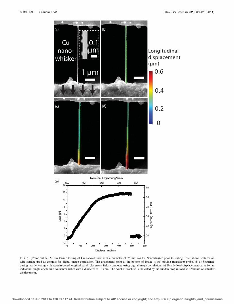
Figure 6 shows snapshots of an in situ tensile test of the75 nm Cu nanowhisker. Figure 6(a) shows the initial testingconfiguration, demonstrating some natural contrast along thelength of the nanowhisker, presumably from a carbonaceouslayer that has formed as a result of imaging. This allows fora local and quasi-full field analysis of the strain that devel-ops upon the application of load to the nanowhisker speci-men. The axial displacement fields are shown in Figs. 6(b)–6(d), which demonstrates that the largest gradients are directlyalong the nanowhisker axis, suggesting good alignment. Inaddition, the axial gradient (used to calculate axial strain) isuniform, which shows that plastic deformation in these Cunanowhiskers does not result in localized necks or heavilyslipped regions. Instead, deformation is primarily elastic un-til the point of fracture at strengths near the ideal strength,which is consistent with the notion of deformation of neardefect-free nanostructures where nucleation of defects, ratherthan activation of pre-existing defects, is the strength con-trolling mechanism.98, 99 Figure 6(e) shows an example of atensile load-displacement curve measured from an individualAu nanowhisker with an effective diameter of 133 nm, whichdemonstrates significant amounts of plastic strain. Knowledgeof the cross-sectional area allows for the calculation of en-gineering stress, and the nominal strain in the wire is alsoshown. Using the system described herein, we have success-fully measured the mechanical response of nanowire speci-mens as small as 60 nm in diameter.36
B. Microcompression of nanoporous gold
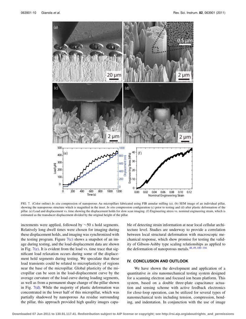
Figure 7 shows in situ microcompression of nanoporousAu specimens in a dual-beam FIB/SEM instrument. Focusedion beam milling using top-down annular patterns was em-ployed to fabricate pillars from bulk nanoporous gold, pre-pared using chemical dealloying of Au-Ag alloys followingthe procedure detailed in Refs. 100–102. For the in situ ex-periments, micropillars were fabricated so that the annularmilling ring intersected with the edge of the bulk specimenas shown in Fig. 7(a). This enabled direct visualization of themicropillar perpendicular to the top surface during deforma-tion (Figs. 7(d) and 7(e)), which greatly simplifies alignmentof the flat punch tip and the specimen, in addition to interpre-tation and strain measurement.
The diamond punch was brought into close proximityto the specimen using the nanopositioning system, and thealignment was verified by performing multiple indents intothe surface of the nanoporous Au away from the micropil-lar specimens. Inspection of the residual imprints on the sur-face indicates the degree of misalignment, which can be cor-rected by using the rotation axis of the microscope stage.Once aligned, the tip is brought to the specimen as shown inFig. 7(d). To optimize image quality and signal-to-noise ratio,the test was performed in a step-wise fashion. Operating infeedback-enabled displacement control, 50 nm displacement
Downloaded 07 Jun 2011 to 130.91.117.41. Redistribution subject to AIP license or copyright; see http://rsi.aip.org/about/rights_and_permissions
063901-9 Gianola et al. Rev. Sci. Instrum. 82, 063901 (2011)
1 µm
Cunano-
whisker
0
0.6
0.4
0.2
Longitudinaldisplacement(µm)
(a) (b)
(c) (d)
0 100 200 300 400 500 600-2
0
2
4
6
8
10
12
14
Load
(µN
)
Displacement (nm)
0.0
0.2
0.4
0.6
0.8
1.0
Engi
neer
ing
Stre
ss(G
Pa)
0.00 0.01 0.02 0.03 0.04
Nominal EngineeringStrain(e)
0.1µm
FIG. 6. (Color online) In situ tensile testing of Cu nanowhisker with a diameter of 75 nm. (a) Cu Nanowhisker prior to testing. Inset shows features onwire surface used as contrast for digital image correlation. The attachment point at the bottom of image is the moving transducer probe. (b–d) Sequenceduring tensile testing with superimposed longitudinal displacement fields computed using digital image correlation. (e) Tensile load-displacement curve for anindividual single crystalline Au nanowhisker with a diameter of 133 nm. The point of fracture is indicated by the sudden drop in load at ∼500 nm of actuatordisplacement.
Downloaded 07 Jun 2011 to 130.91.117.41. Redistribution subject to AIP license or copyright; see http://rsi.aip.org/about/rights_and_permissions
063901-10 Gianola et al. Rev. Sci. Instrum. 82, 063901 (2011)
20 µm
0.5 µm
2 µm
2 µm 2 µm
(a) (b)
(c) (d)
(e)
0 200 400 600 800 1000 1200
0
100
200
300
400
500
Load
(µN
)
Time(s)
0
200
400
600
800
1000
Dis
plac
emen
t(nm
)
0.00 0.02 0.04 0.06 0.08 0.10 0.12
0
10
20
30
40
Eng
ine
eri
ng
Stre
ss(M
Pa)
Nominal Engineering Strain
(f )
FIG. 7. (Color online) In situ compression of nanoporous Au micropillars fabricated using FIB annular milling (a). (b) SEM image of an individual pillar,showing the nanoporous structure which is magnified in the inset. In situ compression configuration (c) prior to testing and (d) after plastic deformation of thepillar. (e) Load and displacement vs. time showing the displacement holds for slow scan imaging. (f) Engineering stress vs. nominal engineering strain, which isestimated as the transducer displacement divided by the original height of the pillar.
increments were applied, followed by ∼50 s hold segments.Relatively long dwell times were chosen for imaging duringthese displacement holds, and imaging was synchronized withthe testing program. Figure 7(c) shows a snapshot of an im-age during testing, and the load-displacement data are shownin Fig. 7(e). It is evident from the load vs. time trace that sig-nificant load relaxation occurs during some of the displace-ment hold segments during testing. We speculate that theseload transients could be related to microplasticity of regionsnear the base of the micropillar. Global plasticity of the mi-cropillar can be seen in the load-displacement curve by theaverage curvature of the load curve during loading segments,as well as from a permanent shape change of the pillar shownin Fig. 7(d). While the majority of plastic deformation wasconcentrated in the lower half of this micropillar, which waspartially shadowed by nanoporous Au residue surroundingthe pillar, this approach provided high quality images capa-
ble of detecting strain information at near local cellular archi-tecture level. Studies are underway to provide a correlationbetween local structural deformation with macroscopic me-chanical response, which show promise for testing the valid-ity of Gibson-Ashby type scaling relationships as applied tothe deformation of nanoporous metals.48, 49, 100–104
IV. CONCLUSION AND OUTLOOK
We have shown the development and application of aquantitative in situ nanomechanical testing system designedfor a scanning electron and focused ion beam platform. Thissystem, based on a double three-plate capacitance actua-tion and sensing scheme with active feedback electronicsfor close-loop operation, can be utilized for several types ofnanomechanical tests including tension, compression, bend-ing, and indentation. In conjunction with the use of image
Downloaded 07 Jun 2011 to 130.91.117.41. Redistribution subject to AIP license or copyright; see http://rsi.aip.org/about/rights_and_permissions
063901-11 Gianola et al. Rev. Sci. Instrum. 82, 063901 (2011)
processing software, the system allows for a quantitative as-sessment of the elastic and plastic response of nanostructures.We demonstrate the efficacy of this characterization platformto the in situ mechanical testing of metal nanowires and FIB-fabricated nanoporous Au micropillars. The application ofthese quantitative methods allows for insights to be gleanedon new mechanisms of deformation that govern the mechani-cal response of small-scale materials.
We envision several future improvements to the nanome-chanical testing system for increased fidelity and versatility.First, the overall size of the transducer and transducer hous-ing will be reduced to minimize the risk of mechanical in-terference with other internal components and to facilitatethe use of other in situ analytical techniques (e.g., EBSD).Through clever design, this can be accomplished withoutcompromising the maximum transducer force. Another im-provement will involve reducing the moving mass and/orincreasing the spring stiffness of the transducer to in turn in-crease the resonance frequency and mechanical bandwidth ofthe transducer. A higher resonance frequency will offer fasterresponse and also be more stable in the high vacuum environ-ment. However, increasing the spring stiffness will place moredemand on displacement sensitivity to not degrade the forcesensitivity.
ACKNOWLEDGMENTS
The authors thank Gunther Richter for providing metalnanowhiskers. Thanks go to Haijun Jin and Simone Schen-del for providing nanoporous Au specimens and preparing thepillars. D.S.G. acknowledges support from an Alexander vonHumboldt Postdoctoral Fellowship and start-up funding fromthe University of Pennsylvania.
1M. D. Uchic, D. M. Dimiduk, J. N. Florando, and W. D. Nix, Science 305,986 (2004).
2D. M. Dimiduk, M. D. Uchic, and T. A. Parthasarathy, Acta Mater. 53,4065 (2005).
3J. R. Greer, W. C. Oliver, and W. D. Nix, Acta Mater. 53, 1821 (2005).4C. A. Volkert and E. T. Lilleodden, Philos. Mag. 86, 5567 (2006).5D. Kiener, C. Motz, T. Schöberl, M. Jenko, and G. Dehm, Adv. Eng.Mater. 8, 1119 (2006).
6S. Brinckmann, J.-Y. Kim, and J. Greer, Phys. Rev. Lett. 100, 155502(2008).
7W. W. Gerberich, J. Michler, W. M. Mook, R. Ghisleni, F. Östlund, D. D.Stauffer, and R. Ballarini, J. Mater. Res. 24, 898 (2009).
8A. Jennings and J. Greer, Philos. Mag. 1108, 1 (2010).9A. T. Jennings, M. J. Burek, and J. R. Greer, Phys. Rev. Lett. 104, (2010).
10J.-Y. Kim and J. R. Greer, Appl. Phys. Lett. 93, 101916 (2008).11C. Motz, D. Weygand, J. Senger, and P. Gumbsch, Acta Mater. 56, 1942
(2008).12A. Schneider, D. Kaufmann, B. Clark, C. Frick, P. Gruber, R. Mönig,
O. Kraft, and E. Arzt, Phys. Rev. Lett. 103, (2009).13B. E. Schuster, Q. Wei, T. C. Hufnagel, and K. T. Ramesh, Acta Mater. 56,
5091 (2008).14C. A. Volkert, A. Donohue, and F. Spaepen, J. Appl. Phys. 103, 083539
(2008).15D. S. Gianola and C. Eberl, JOM 61, 24 (2009).16W. C. Oliver and G. M. Pharr, J. Mater. Res. 19, 3 (2004).17M. Uchic, P. Shade, and D. Dimiduk, Annu. Rev. Mater. Res. 39, 361
(2009).18O. Kraft, P. Gruber, R. Mönig, and D. Weygand, Annu. Rev. Mater. Res.
40, 293 (2010).19M. D. Uchic, D. M. Dimiduk, R. Wheeler, P. A. Shade, and H. L. Fraser,
Scr. Mater. 54, 759 (2006).
20S. T. Motz C and P. R, Acta Mater. 53, 4269 (2005).21F. Weber, I. Schestakow, F. Roters, and D. Raabe, Adv. Eng. Mater. 10,
737 (2008).22B. Wu, A. Heidelberg, and J. J. Boland, Nat. Mater. 4, 525 (2005).23D. Kiener, W. Grosinger, G. Dehm, and R. Pippan, Acta Mater. 56, 580
(2008).24K. J. Hemker and W. N. Sharpe, Annu. Rev. Mater. Res. 37, 93 (2007).25W. N. Sharpe, K. T. Turner, and R. L. Edwards, Exp. Mech. 39, 162
(1999).26Y. Ganesan, Y. Lu, C. Peng, H. Lu, R. Ballarini, and J. Lou, J. Microelec-
tromech. Syst. 19, 675 (2010).27Sé. Gravier, M. Coulombier, A. Safi, N. Andre, A. BoÉ, J.-P. Raskin, and
T. Pardoen, J. Microelectromech. Syst. 18, 555 (2009).28D. Zhang, J.-M. Breguet, R. Clavel, V. Sivakov, S. Christiansen, and J.
Michler, J. Microelectromech. Syst. 19, 663 (2010).29C. Ke and H. D. Espinosa, Small 2, 1484 (2006).30B. Peng, M. Locascio, P. Zapol, S. Li, S. L. Mielke, G. C. Schatz, and
H. D. Espinosa, Nat. Nanotech. 3, 626 (2008).31Y. Zhu, C. Ke, and H. D. Espinosa, Exp. Mech. 47, 7 (2007).32I. Chasiotis and W. Knauss, Exp. Mech. 42, 51 (2002).33M. Naraghi, T. Ozkan, I. Chasiotis, S. Hazra, and M. de Boer, J. Mi-
cromech. Microeng. 20, 125022 (2010).34U. Singh, V. Prakash, A. R. Abramson, W. Chen, L. Qu, and L. Dai, Appl.
Phys. Lett. 89, 073103 (2006).35S. Orso, U. G. K. Wegst, C. Eberl, and E. Arzt, Adv. Mater. 18, 874
(2006).36G. Richter, K. Hillerich, D. S. Gianola, R. Mönig, O. Kraft, and C. A.
Volkert, Nano Lett. 9, 3048 (2009).37M. Legros, D. Gianola, and C. Motz, MRS Bull. 35, 354 (2010).38K. A. Rzepiejewska-Malyska, G. Buerki, J. Michler, R. C. Major, E.
Cyrankowski, S. A. S. Asif, and O. L. Warren, J. Mater. Res. 23, 1973(2008).
39J. Michler, K. Wasmer, S. Meier, F. Östlund, and K. Leifer, Appl. Phys.Lett. 90, 043123 (2007).
40J. Nowak, K. Rzepiejewska-Malyska, R. Major, O. Warren, and J. Michler,Mater. Today 12, 44 (2010).
41A. M. Minor, E. T. Lilleodden, M. Jin, E. A. Stach, D. C. Chrzan, and J.W. M. Jr, Philos. Mag. 85, 323 (2005).
42A. M. Minor, E. T. Lilleodden, E. A. Stach, and J. W. M. Jr, J. Mater. Res.19, 176 (2004).
43A. M. Minor, S. A. S. Asif, Z. Shan, E. A. Stach, E. Cyrankowski, T. J.Wyrobek, and O. L. Warren, Nat. Mater. 5, 697 (2006).
44S. H. Oh, M. Legros, D. Kiener, and G. Dehm, Nat. Mater. 8, 95(2009).
45Z. W. Shan, R. K. Mishra, S. A. Syed Asif, O. L. Warren, and A. M. Minor,Nat. Mater. 7, 115 (2008).
46Z. W. Shan, G. Adesso, A. Cabot, M. P. Sherburne, S. A. Syed Asif, O. L.Warren, D. C. Chrzan, A. M. Minor, and A. P. Alivisatos, Nat. Mater. 7,947 (2008).
47Z. W. Shan, J. Li, Y. Q. Cheng, A. M. Minor, S. A. Syed Asif, O. L.Warren, and E. Ma, Phys. Rev. B 77, 155419 (2008).
48Y. Sun, J. Ye, A. M. Minor, and T. J. Balk, Microsc. Res. Tech. 72, 232(2009).
49Y. Sun, J. Ye, Z. Shan, A. M. Minor, and T. J. Balk, JOM J. Miner., Met.Mater. Soc. 59, 54 (2007).
50Y. B. Wang, B. Q. Li, M. L. Sui, and S. X. Mao, Appl. Phys. Lett. 92,011903 (2008).
51J. Ye, R. K. Mishra, A. R. Pelton, and A. M. Minor, Acta Mater. 58, 490(2010).
52M. Legros, M. Cabie, and D. S. Gianola, Microsc. Res. Tech. 72, 270(2009).
53J. Deneen, W. M. Mook, A. Minor, W. W. Gerberich, and C. Barry Carter,J. Mater. Sci. 41, 4477 (2006).
54X. Li, I. Chasiotis, and T. Kitamura, MRS Bull. 35, 361 (2010).55R. Spolenak, W. Ludwig, J. Buffiere, and J. Michler, MRS Bull. 35, 368
(2010).56R. Maaß, S. Van Petegem, D. Grolimund, H. Van Swygenhoven, D.
Kiener, and G. Dehm, Appl. Phys. Lett. 92, 071905 (2008).57R. Maaß, S. Van Petegem, H. Van Swygenhoven, P. Derlet, C. Volkert, and
D. Grolimund, Phys. Rev. Lett. 99, 145505 (2007).58K. Wasmer, T. Wermelinger, A. Bidiville, R. Spolenak, and J. Michler, J.
Mater. Res. 23, 3040 (2008).59American Society of Testing and Materials, ASTM E 8M, 1995.60M. A. Haque and M. T. A. Saif, Scr. Mater. 47, 863 (2002).
Downloaded 07 Jun 2011 to 130.91.117.41. Redistribution subject to AIP license or copyright; see http://rsi.aip.org/about/rights_and_permissions
063901-12 Gianola et al. Rev. Sci. Instrum. 82, 063901 (2011)
61T. E. Buchheit, S. J. Glass, J. R. Sullivan, S. S. Mani, D. A. Lavan, T. A.Friedmann, and R. Janek, J. Mater. Sci. 38, 4081 (2003).
62W. N. Sharpe, B. Yuan, and R. L. Edwards, J. Microelectromech. Syst. 6,193 (1997).
63E. P. S. Tan and C. T. Lim, Rev. Sci. Instrum. 75, 2581 (2004).64H. Miyazaki and K. Hayashi, Biomed. Microdevices 2, 151 (1999).65M. F. Yu, O. Lourie, M. J. Dyer, K. Moloni, T. F. Kelly, and R. S. Ruoff,
Science 287, 637 (2000).66M. D. Wang, H. Yin, R. Landick, J. Gelles, and S. M. Block, Biophys. J.
72, 1335 (1997).67H. D. Espinosa, B. C. Prorok, and M. Fischer, J. Mech. Phys. Solids 51,
47 (2003).68S. S. Brenner, J. Appl. Phys. 27, 1484 (1956).69R. Longtin, C. Fauteux, J. Pegna, and M. Boman, Carbon 42, 2905
(2004).70W. Suwito, M. Dunn, S. Cunningham, and D. Read, J. Appl. Phys. 85,
3519 (1999).71T. Zhang, Y. Su, C. Qian, M. Zhao, and L. Chen, Acta Mater. 48, 2843
(2000).72C. A. Volkert and A. M. Minor, MRS Bull. 32, 389 (2007).73H. Hiroshima, N. Suzuki, N. Ogawa, and M. Komuro, Jpn. J. Appl. Phys.,
Part 1 38, 7135 (1999).74V. Gopal, V. Radmilovic, C. Daraio, S. Jin, P. Yang, and E. Stach, Nano
Lett. 4, 2059 (2004).75Introduction to Focused Ion Beams: Instrumentation, Theory, Techniques
and Practice, edited by F. A. S. L. A. Giannuzzi (Springer, New York,2005).
76H. Bei, S. Shim, M. K. Miller, G. M. Pharr, and E. P. George, Appl. Phys.Lett. 91, 111915 (2007).
77B. Moser, K. Wasmer, L. Barbieri, and J. Michler, J. Mater. Res. 22, 1004(2007).
78M. D. Uchic and D. M. Dimiduk, Mater. Sci. Eng. A 400–401, 268(2005).
79V. Gopal, E. Stach, V. Radmilovic, and I. Mowat, Appl. Phys. Lett. 85, 49(2004).
80I. Utke, V. Friedli, S. Fahlbusch, S. Hoffmann, P. Hoffmann, and J. Mich-ler, Adv. Eng. Mater. 8, 155 (2006).
81O. Warren, S. Downs, and T. Wyrobek, Z. Metallkd. 95, 287 (2004).82Y. Oh, M. R. Wilson, R. C. Major, S. A. S. Asif, and O. L. Warren, U.S.
Patent No. US 2010/0036636 A1 (2010).
83M. A. Sutton, J.-J. Orteu, and H. Schreier, Image Correlation for Shape,Motion and Deformation Measurements: Basic Concepts, Theory and Ap-plications, 1st ed. (Springer, New York, 2009).
84T. C. Chu, W. F. Ranson, M. A. Sutton, and W. H. Peters, Exp. Mech. 25,232 (1985).
85W. H. Peters and W. F. Ranson, Opt. Eng. 21, 427 (1982).86H. A. Bruck, S. R. McNeill, M. A. Sutton, and W. H. P. III, Exp. Mech.
29, 261 (1989).87W. N. Sharpe, J. Pulskamp, D. S. Gianola, C. Eberl, R. Polawich, and R.
Thompson, Exp. Mech. 47, 649 (2006).88C. Eberl, D. S. Gianola, and R. Thompson, MATLAB file exchange,
http://www.mathworks.com/matlabcentral/fileexchange/12413 (2006).89N. Biery, M. de Graef, and T. Pollock, Metall. Mater. Trans. A 34, 2301
(2003).90M. A. Sutton, N. Li, D. C. Joy, A. P. Reynolds, and X. Li, Exp. Mech. 47,
775 (2007).91M. A. Sutton, N. Li, D. Garcia, N. Cornille, J. J. Orteu, S. R. Mc-
Neill, H. W. Schreier, X. Li, and A. P. Reynolds, Exp. Mech. 47, 789(2007).
92B. G. Clark, D. S. Gianola, O. Kraft, and C. P. Frick, Adv. Eng. Mater. 12,808 (2010).
93W. A. Scrivens, Y. Luo, M. A. Sutton, S. A. Collette, M. L. Myrick, P.Miney, P. E. Colavita, A. P. Reynolds, and X. Li, Exp. Mech. 47, 63(2006).
94S. S. Brenner, Acta Metall. 4, 62 (1956).95S. S. Brenner, J. Appl. Phys. 28, 1023 (1957).96S. S. Brenner, J. Appl. Phys. 30, 266 (1958).97S. S. Brenner and G. W. Sears, Acta Metall. 4, 268 (1956).98H. Bei, S. Shim, E. P. George, M. K. Miller, E. G. Herbert, and G. M.
Pharr, Scr. Mater. 57, 397 (2007).99T. Zhu, J. Li, A. Samanta, A. Leach, and K. Gall, Phys. Rev. Lett. 100,
025502 (2008).100C. A. Volkert, E. T. Lilleodden, D. Kramer, and J. Weissmüller, Appl.
Phys. Lett. 89, 061920 (2006).101J. Biener, A. M. Hodge, J. R. Hayes, C. A. Volkert, L. A. Zepeda-Ruiz, A.
V. Hamza, and F. F. Abraham, Nano Lett. 6, 2379 (2006).102C. A. Volkert and E. T. Lilleodden, Philos. Mag. 86, 5567 (2006).103T. J. Balk, C. Eberl, Y. Sun, K. J. Hemker, and D. S. Gianola, JOM J.
Miner., Met. Mater. Soc. 61, 26 (2009).104A. Mathur and J. Erlebacher, Appl. Phys. Lett. 90, 061910 (2007).
Downloaded 07 Jun 2011 to 130.91.117.41. Redistribution subject to AIP license or copyright; see http://rsi.aip.org/about/rights_and_permissions