Embed Size (px)
Citation preview
User's GuideSBOU126–April 2012
INA3221EVM Evaluation Board and Software Tutorial
This user's guide describes the characteristics, operation, and use of the INA3221EVM evaluation board.It discusses how to set up and configure the software and hardware, and reviews various aspects of theprogram operation.
Throughout this document, the terms evaluation board, evaluation module, and EVM are synonymous withthe INA3221EVM. This user's guide also includes information regarding operating procedures andinput/output connections, an electrical schematic, printed circuit board (PCB) layout drawings, and a partslist for the EVM.
Contents1 Overview ..................................................................................................................... 32 INA3221EVM Hardware Setup ............................................................................................ 43 INA3221EVM Hardware Overview ........................................................................................ 64 INA3221EVM Software Setup ........................................................................................... 115 INA3221EVM Software Overview ....................................................................................... 146 INA3221EVM Documentation ............................................................................................ 18
List of Figures
1 Hardware Included with INA3221EVM Kit ............................................................................... 3
2 INA3221EVM Hardware Setup............................................................................................ 4
3 INA3221EVM Test Board Block Diagram................................................................................ 5
4 SM-USB-DIG Platform Block Diagram ................................................................................... 6
5 Typical INA3221EVM Hardware Test Connections .................................................................... 7
6 Confirmation of SM-USB-DIG Platform Driver Installation............................................................. 8
7 Connecting the USB Cable to the SM-USB-DIG Platform............................................................. 8
8 INA3221EVM Default Jumper Settings .................................................................................. 9
9 INA3221 Shunt Configurations .......................................................................................... 11
10 INA3221EVM Software Installation Window ........................................................................... 12
11 INA3221EVM License Agreements ..................................................................................... 13
12 INA3221EVM Software Installation Progress .......................................................................... 13
13 INA3221EVM Software Interface ........................................................................................ 14
14 INA3221EVM Software: Communication Error with the SM-USB-DIG Platform .................................. 15
15 INA3221 Results Bar...................................................................................................... 15
16 Registers Tab .............................................................................................................. 16
17 Graphing INA3221 Data .................................................................................................. 17
18 Auto-Write, Power Button, and Voltage Control ....................................................................... 17
19 INA3221EVM Schematic ................................................................................................. 18
20 INA3221EVM PCB Top Layer (Component Side) .................................................................... 19
List of Tables
1 INA3221EVM Kit Contents................................................................................................. 3Microsoft, Windows are registered trademarks of Microsoft Corporation.I2C is a trademark of NXP Semiconductors.WinZIP is a registered trademark of WinZip International LLC.All other trademarks are the property of their respective owners.
1SBOU126–April 2012 INA3221EVM Evaluation Board and Software TutorialSubmit Documentation Feedback
Copyright © 2012, Texas Instruments Incorporated
www.ti.com
2 Related Documentation .................................................................................................... 4
3 Pin Connections............................................................................................................. 5
4 INA3221EVM Test Board Jumper Functions .......................................................................... 10
5 Bill of Materials ............................................................................................................ 20
2 INA3221EVM Evaluation Board and Software Tutorial SBOU126–April 2012Submit Documentation Feedback
Copyright © 2012, Texas Instruments Incorporated
USB Extender Cable
SM-USB-DIG Connector Ribbon Cable
SM-USB-DIG
INA3221EVM Board
www.ti.com Overview
1 Overview
The INA3221 is a three-channel, high-side current sensor and bus voltage monitor with an I2C™ interface.The INA3221 monitors both shunt drops and bus supply voltages with programmable conversion timesand averaging modes. The INA3221 offers both critical and warning alerts to detect multipleprogrammable out-of-range conditions for each channel.
This document gives a general overview of the INA3221EVM, and provides a general description of thefeatures and functions to be considered while using this evaluation module.
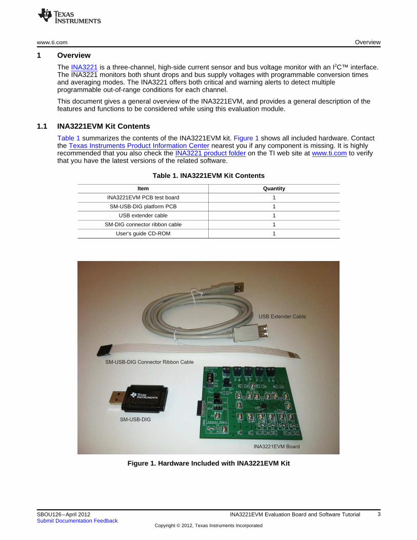
1.1 INA3221EVM Kit Contents
Table 1 summarizes the contents of the INA3221EVM kit. Figure 1 shows all included hardware. Contactthe Texas Instruments Product Information Center nearest you if any component is missing. It is highlyrecommended that you also check the INA3221 product folder on the TI web site at www.ti.com to verifythat you have the latest versions of the related software.
Table 1. INA3221EVM Kit Contents
Item Quantity
INA3221EVM PCB test board 1
SM-USB-DIG platform PCB 1
USB extender cable 1
SM-DIG connector ribbon cable 1
User’s guide CD-ROM 1
Figure 1. Hardware Included with INA3221EVM Kit
3SBOU126–April 2012 INA3221EVM Evaluation Board and Software TutorialSubmit Documentation Feedback
Copyright © 2012, Texas Instruments Incorporated
INA3221EVM Hardware Setup www.ti.com
1.2 Related Documentation from Texas Instruments
The following documents provide information regarding Texas Instruments' integrated circuits used inassembly of the INA3221EVM. This user's guide is available from www.ti.com under literature numberSBOU126. Any letter appended to the literature number corresponds to the document revision that iscurrent at the time of the writing of this document. Newer revisions may be available from www.ti.com, orcall the Texas Instruments Literature Response Center at (800) 477-8924 or the Product InformationCenter at (972) 644-5580. When ordering, identify the document by both title and literature number.
Table 2. Related Documentation
Document Literature Number
INA3221 product data sheet SBOS576
SM-USB-DIG platform user guide SBOU098
USB DIG platform user's guide SBOU058
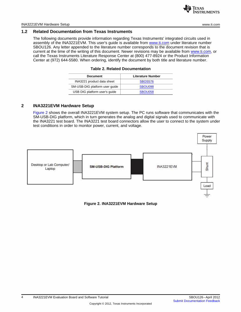
2 INA3221EVM Hardware Setup
Figure 2 shows the overall INA3221EVM system setup. The PC runs software that communicates with theSM-USB-DIG platform, which in turn generates the analog and digital signals used to communicate withthe INA3221 test board. The INA3221 test board connectors allow the user to connect to the system undertest conditions in order to monitor power, current, and voltage.
Figure 2. INA3221EVM Hardware Setup
4 INA3221EVM Evaluation Board and Software Tutorial SBOU126–April 2012Submit Documentation Feedback
Copyright © 2012, Texas Instruments Incorporated
INA3221
V Supply
(DVDD)DUT
I C Interface2
10-Pin FemaleSM-USB-DIG
Connector
J5/J6
J3/J4
J1
Shunt Terminals
T3/T4
4
I C AddressJumpers
2
A0
A1
www.ti.com INA3221EVM Hardware Setup
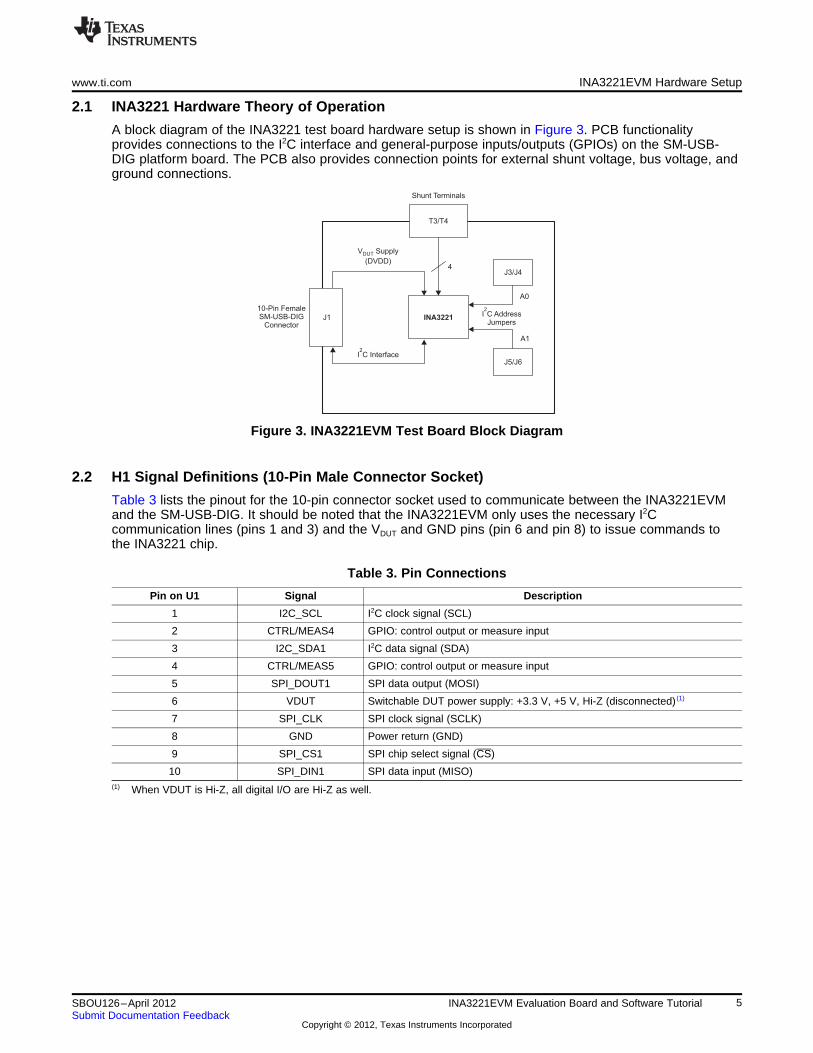
2.1 INA3221 Hardware Theory of Operation
A block diagram of the INA3221 test board hardware setup is shown in Figure 3. PCB functionalityprovides connections to the I2C interface and general-purpose inputs/outputs (GPIOs) on the SM-USB-DIG platform board. The PCB also provides connection points for external shunt voltage, bus voltage, andground connections.
Figure 3. INA3221EVM Test Board Block Diagram
2.2 H1 Signal Definitions (10-Pin Male Connector Socket)
Table 3 lists the pinout for the 10-pin connector socket used to communicate between the INA3221EVMand the SM-USB-DIG. It should be noted that the INA3221EVM only uses the necessary I2Ccommunication lines (pins 1 and 3) and the VDUT and GND pins (pin 6 and pin 8) to issue commands tothe INA3221 chip.
Table 3. Pin Connections
Pin on U1 Signal Description
1 I2C_SCL I2C clock signal (SCL)
2 CTRL/MEAS4 GPIO: control output or measure input
3 I2C_SDA1 I2C data signal (SDA)
4 CTRL/MEAS5 GPIO: control output or measure input
5 SPI_DOUT1 SPI data output (MOSI)
6 VDUT Switchable DUT power supply: +3.3 V, +5 V, Hi-Z (disconnected) (1)
7 SPI_CLK SPI clock signal (SCLK)
8 GND Power return (GND)
9 SPI_CS1 SPI chip select signal (CS)
10 SPI_DIN1 SPI data input (MISO)(1) When VDUT is Hi-Z, all digital I/O are Hi-Z as well.
5SBOU126–April 2012 INA3221EVM Evaluation Board and Software TutorialSubmit Documentation Feedback
Copyright © 2012, Texas Instruments Incorporated
TUSB32108052 Microcontrollerwith USB Interface
and UART
USB Busfrom Computer
3.3-VRegulator
+3.3 VUSB
+5.0 V
8-K 8-ByteEEPROM
´
Buffers andLevel
Translators
PowerSwitching
Vdut(Hi-Z, 3.3V or 5V)
Switched Power
I CSPIControl BitsMeasure Bits
2
Power-OnReset
SM-USB-DIG
To Test Board
To Computerand Power Supplies
+3.3 V
USB +5.0 V
INA3221EVM Hardware Overview www.ti.com
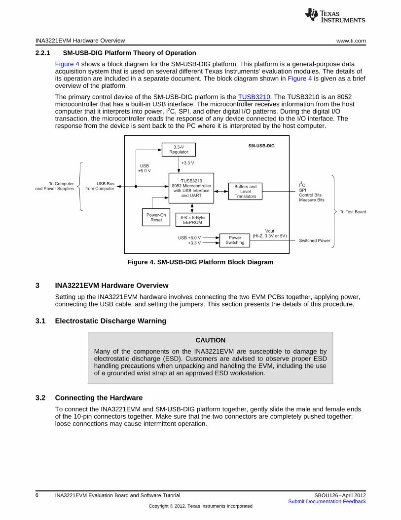
2.2.1 SM-USB-DIG Platform Theory of Operation
Figure 4 shows a block diagram for the SM-USB-DIG platform. This platform is a general-purpose dataacquisition system that is used on several different Texas Instruments' evaluation modules. The details ofits operation are included in a separate document. The block diagram shown in Figure 4 is given as a briefoverview of the platform.
The primary control device of the SM-USB-DIG platform is the TUSB3210. The TUSB3210 is an 8052microcontroller that has a built-in USB interface. The microcontroller receives information from the hostcomputer that it interprets into power, I2C, SPI, and other digital I/O patterns. During the digital I/Otransaction, the microcontroller reads the response of any device connected to the I/O interface. Theresponse from the device is sent back to the PC where it is interpreted by the host computer.
Figure 4. SM-USB-DIG Platform Block Diagram
3 INA3221EVM Hardware Overview
Setting up the INA3221EVM hardware involves connecting the two EVM PCBs together, applying power,connecting the USB cable, and setting the jumpers. This section presents the details of this procedure.
3.1 Electrostatic Discharge Warning
CAUTION
Many of the components on the INA3221EVM are susceptible to damage byelectrostatic discharge (ESD). Customers are advised to observe proper ESDhandling precautions when unpacking and handling the EVM, including the useof a grounded wrist strap at an approved ESD workstation.
3.2 Connecting the Hardware
To connect the INA3221EVM and SM-USB-DIG platform together, gently slide the male and female endsof the 10-pin connectors together. Make sure that the two connectors are completely pushed together;loose connections may cause intermittent operation.
6 INA3221EVM Evaluation Board and Software Tutorial SBOU126–April 2012Submit Documentation Feedback
Copyright © 2012, Texas Instruments Incorporated

www.ti.com INA3221EVM Hardware Overview
3.3 Connecting Power
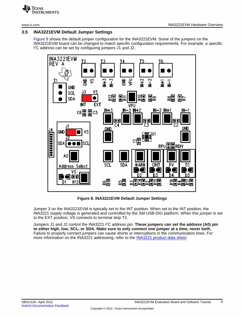
After the EVM and SM-USB-DIG are conjoined, as shown in Figure 5, connect the channels intended tobe measured. The source for VIN is not included with the kit, and its voltage may differ depending onspecific testing requirements.
Figure 5. Typical INA3221EVM Hardware Test Connections
7SBOU126–April 2012 INA3221EVM Evaluation Board and Software TutorialSubmit Documentation Feedback
Copyright © 2012, Texas Instruments Incorporated
INA3221EVM Hardware Overview www.ti.com
3.4 Connecting the USB Cable to the SM-USB-DIG Platform
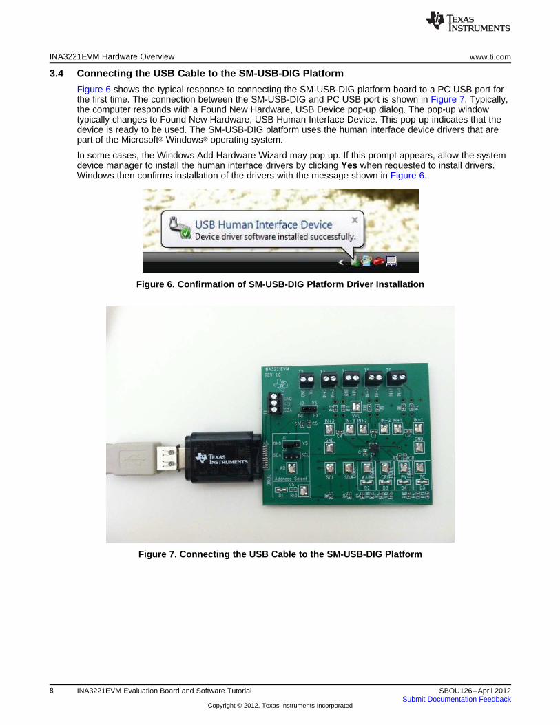
Figure 6 shows the typical response to connecting the SM-USB-DIG platform board to a PC USB port forthe first time. The connection between the SM-USB-DIG and PC USB port is shown in Figure 7. Typically,the computer responds with a Found New Hardware, USB Device pop-up dialog. The pop-up windowtypically changes to Found New Hardware, USB Human Interface Device. This pop-up indicates that thedevice is ready to be used. The SM-USB-DIG platform uses the human interface device drivers that arepart of the Microsoft® Windows® operating system.
In some cases, the Windows Add Hardware Wizard may pop up. If this prompt appears, allow the systemdevice manager to install the human interface drivers by clicking Yes when requested to install drivers.Windows then confirms installation of the drivers with the message shown in Figure 6.
Figure 6. Confirmation of SM-USB-DIG Platform Driver Installation
Figure 7. Connecting the USB Cable to the SM-USB-DIG Platform
8 INA3221EVM Evaluation Board and Software Tutorial SBOU126–April 2012Submit Documentation Feedback
Copyright © 2012, Texas Instruments Incorporated
www.ti.com INA3221EVM Hardware Overview
3.5 INA3221EVM Default Jumper Settings
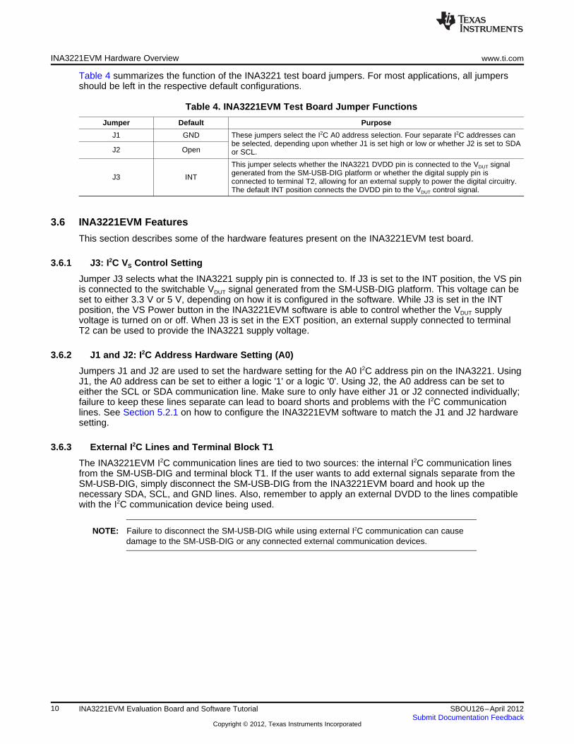
Figure 8 shows the default jumper configuration for the INA3221EVM. Some of the jumpers on theINA3221EVM board can be changed to match specific configuration requirements. For example, a specificI2C address can be set by configuring jumpers J1 and J2.
Figure 8. INA3221EVM Default Jumper Settings
Jumper 3 on the INA3221EVM is typically set to the INT position. When set to the INT position, theINA3221 supply voltage is generated and controlled by the SM-USB-DIG platform. When this jumper is setto the EXT position, VS connects to terminal strip T2.
Jumpers J1 and J2 control the INA3221 I2C address pin. These jumpers can set the address (A0) pinto either high, low, SCL, or SDA. Make sure to only connect one jumper at a time, never both.Failure to properly connect jumpers can cause shorts or interruptions in the communication lines. Formore information on the INA3221 addressing, refer to the INA3221 product data sheet.
9SBOU126–April 2012 INA3221EVM Evaluation Board and Software TutorialSubmit Documentation Feedback
Copyright © 2012, Texas Instruments Incorporated
INA3221EVM Hardware Overview www.ti.com
Table 4 summarizes the function of the INA3221 test board jumpers. For most applications, all jumpersshould be left in the respective default configurations.
Table 4. INA3221EVM Test Board Jumper Functions
Jumper Default Purpose
J1 GND These jumpers select the I2C A0 address selection. Four separate I2C addresses canbe selected, depending upon whether J1 is set high or low or whether J2 is set to SDA
J2 Open or SCL.
This jumper selects whether the INA3221 DVDD pin is connected to the VDUT signalgenerated from the SM-USB-DIG platform or whether the digital supply pin isJ3 INT connected to terminal T2, allowing for an external supply to power the digital circuitry.The default INT position connects the DVDD pin to the VDUT control signal.
3.6 INA3221EVM Features
This section describes some of the hardware features present on the INA3221EVM test board.
3.6.1 J3: I2C VS Control Setting
Jumper J3 selects what the INA3221 supply pin is connected to. If J3 is set to the INT position, the VS pinis connected to the switchable VDUT signal generated from the SM-USB-DIG platform. This voltage can beset to either 3.3 V or 5 V, depending on how it is configured in the software. While J3 is set in the INTposition, the VS Power button in the INA3221EVM software is able to control whether the VDUT supplyvoltage is turned on or off. When J3 is set in the EXT position, an external supply connected to terminalT2 can be used to provide the INA3221 supply voltage.
3.6.2 J1 and J2: I2C Address Hardware Setting (A0)
Jumpers J1 and J2 are used to set the hardware setting for the A0 I2C address pin on the INA3221. UsingJ1, the A0 address can be set to either a logic '1' or a logic '0'. Using J2, the A0 address can be set toeither the SCL or SDA communication line. Make sure to only have either J1 or J2 connected individually;failure to keep these lines separate can lead to board shorts and problems with the I2C communicationlines. See Section 5.2.1 on how to configure the INA3221EVM software to match the J1 and J2 hardwaresetting.
3.6.3 External I2C Lines and Terminal Block T1
The INA3221EVM I2C communication lines are tied to two sources: the internal I2C communication linesfrom the SM-USB-DIG and terminal block T1. If the user wants to add external signals separate from theSM-USB-DIG, simply disconnect the SM-USB-DIG from the INA3221EVM board and hook up thenecessary SDA, SCL, and GND lines. Also, remember to apply an external DVDD to the lines compatiblewith the I2C communication device being used.
NOTE: Failure to disconnect the SM-USB-DIG while using external I2C communication can causedamage to the SM-USB-DIG or any connected external communication devices.
10 INA3221EVM Evaluation Board and Software Tutorial SBOU126–April 2012Submit Documentation Feedback
Copyright © 2012, Texas Instruments Incorporated
www.ti.com INA3221EVM Software Setup
3.6.4 Shunt Monitor Configuration and Terminal Blocks T3, T5, and T6
The INA3221 is typically used in a high-side shunt configuration, as shown in Figure 9. Terminal blocksT3, T5, and T6 represent VIN+ and VIN– for channels 1, 2, and 3, respectively. Depending on applicationrequirements, either of these configurations may be used without applying changes to the INA3221EVMboard or software.
Figure 9. INA3221 Shunt Configurations
4 INA3221EVM Software Setup
This section discusses how to install the INA3221EVM software.
4.1 INA3221EVM Software Operating Systems
The INA3221EVM software has been tested on Microsoft® Windows® XP operating systems (OS) withUnited States and European regional settings. The software should also function on other Windows OSplatforms.
11SBOU126–April 2012 INA3221EVM Evaluation Board and Software TutorialSubmit Documentation Feedback
Copyright © 2012, Texas Instruments Incorporated

INA3221EVM Software Setup www.ti.com
4.2 Software Installation
The INA3221EVM software is included on the CD shipped with the EVM kit. It is also available through theINA3221EVM product folder on www.ti.com. To install the software to your system, insert the disc into anavailable CD-ROM drive. Navigate to the drive contents and open the INA3221EVM software folder.Locate the compressed file (INA3221EVM.zip) and open it. Using WinZIP®, or a similar file compressionprogram, extract the INA3221EVM files into a specific INA3221EVM folder (for example, C:\INA3221EVM)on your hard drive.
When the files are extracted, navigate to the INA3221EVM folder you created on the hard drive. Locatethe setup.exe file and execute it to start the installation. The INA3221 software installer file then begins theinstallation process, as shown in Figure 10.
Figure 10. INA3221EVM Software Installation Window
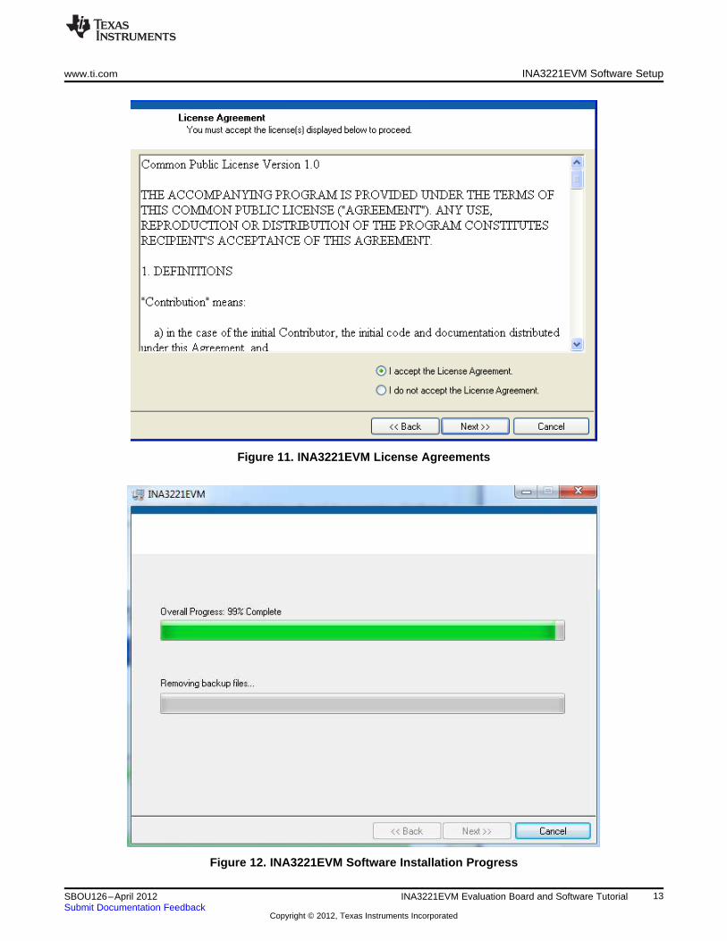
After the installation process initializes, the user is given the choice of selecting the directory in which toinstall the program; the default location is C:\Program Files\INA3221\ and C:\Program Files\NationalInstruments\. Following this option, two license agreements are presented that must be accepted, asillustrated in Figure 11. After accepting the Texas Instruments and National Instruments licenseagreements, the progress bar opens and shows the installation of the software, refer to Figure 12. Whenthe installation process is completed, click Finish.
12 INA3221EVM Evaluation Board and Software Tutorial SBOU126–April 2012Submit Documentation Feedback
Copyright © 2012, Texas Instruments Incorporated
www.ti.com INA3221EVM Software Setup
Figure 11. INA3221EVM License Agreements
Figure 12. INA3221EVM Software Installation Progress
13SBOU126–April 2012 INA3221EVM Evaluation Board and Software TutorialSubmit Documentation Feedback
Copyright © 2012, Texas Instruments Incorporated
INA3221EVM Software Overview www.ti.com
5 INA3221EVM Software Overview
This section discusses how to use the INA3221EVM software. Software operation involves a two-stepprocess: INA3221 configuration and operation.
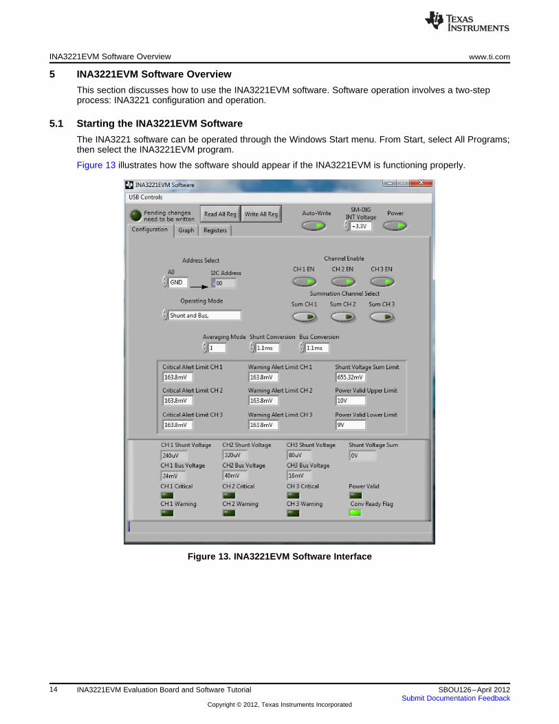
5.1 Starting the INA3221EVM Software
The INA3221 software can be operated through the Windows Start menu. From Start, select All Programs;then select the INA3221EVM program.
Figure 13 illustrates how the software should appear if the INA3221EVM is functioning properly.
Figure 13. INA3221EVM Software Interface
14 INA3221EVM Evaluation Board and Software Tutorial SBOU126–April 2012Submit Documentation Feedback
Copyright © 2012, Texas Instruments Incorporated

www.ti.com INA3221EVM Software Overview
Figure 14 shows an error window that pops up if the computer cannot communicate with the EVM. If thiserror is received, first ensure that the USB cable is properly connected on both ends. This error can alsooccur if the USB cable is connected before the SM-USB-DIG platform power source. Another possiblesource for this error is a problem with the PC USB Human Interface Device driver. Make sure that thedevice is recognized when the USB cable is plugged in; recognition is indicated by a Windows-generatedconfirmation sound.
Figure 14. INA3221EVM Software: Communication Error with the SM-USB-DIG Platform
5.2 Using the INA3221EVM Software
This section describes the basic operation of the device, and offers guidelines for interpreting the graphicuser interface (GUI).
5.2.1 INA3221 Bus Voltage, Shunt Voltage, and Shunt Voltage Sum Reading Bar
The bottom bar of the INA3221 software, as shown in Figure 15, allows the user to constantly check thestatus of the INA3221 device. These values are updated each time the Read All Reg button is pressed atthe top of the software. In addition to the register values stored in the device, the software also includesflags for when the device is ready to trigger another conversion and when the Critical, Warning, andPower Valid flags are triggered.
Figure 15. INA3221 Results Bar
15SBOU126–April 2012 INA3221EVM Evaluation Board and Software TutorialSubmit Documentation Feedback
Copyright © 2012, Texas Instruments Incorporated
INA3221EVM Software Overview www.ti.com
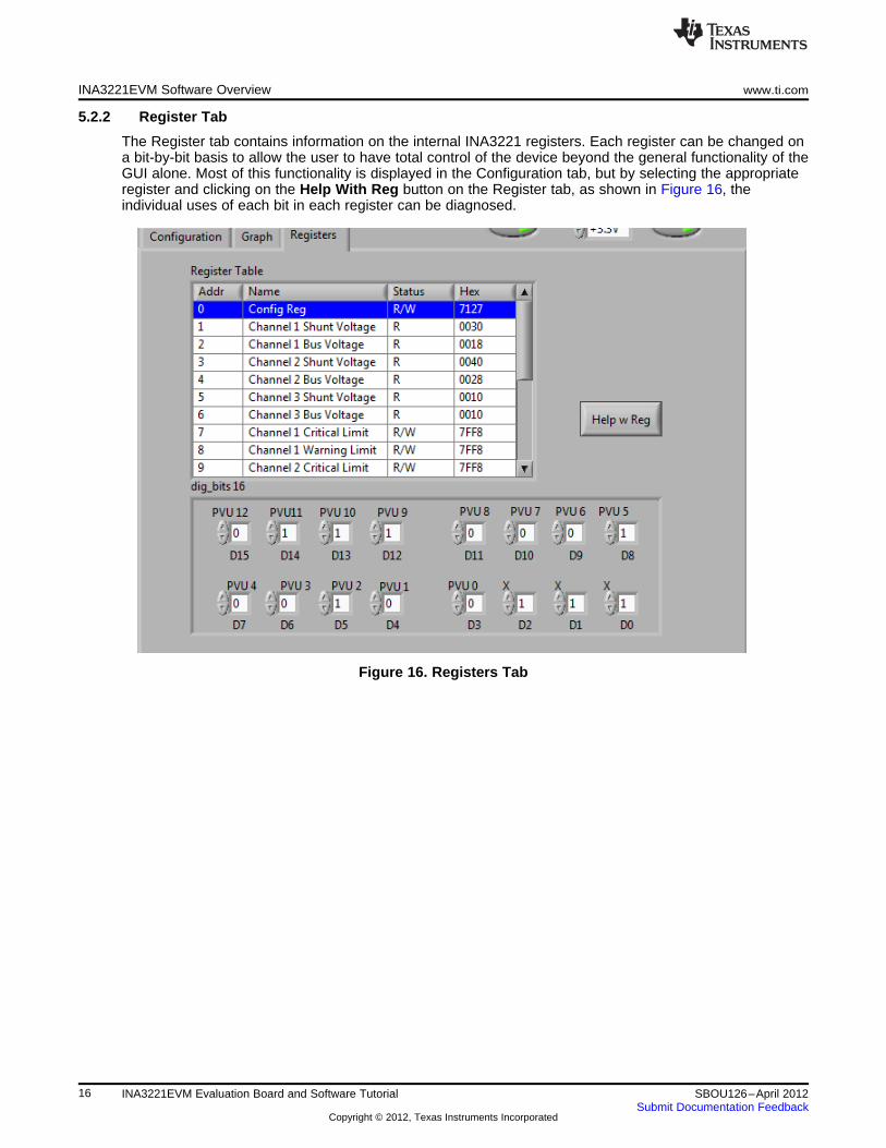
5.2.2 Register Tab
The Register tab contains information on the internal INA3221 registers. Each register can be changed ona bit-by-bit basis to allow the user to have total control of the device beyond the general functionality of theGUI alone. Most of this functionality is displayed in the Configuration tab, but by selecting the appropriateregister and clicking on the Help With Reg button on the Register tab, as shown in Figure 16, theindividual uses of each bit in each register can be diagnosed.
Figure 16. Registers Tab
16 INA3221EVM Evaluation Board and Software Tutorial SBOU126–April 2012Submit Documentation Feedback
Copyright © 2012, Texas Instruments Incorporated

www.ti.com INA3221EVM Software Overview
5.2.3 Graph Tab
The Graph tab, shown in Figure 17, contains a plot window that shows the progression of data over timeon the INA3221. All seven variables at the bottom of the EVM software (CH1 VSHUNT, CH2 VSHUNT, CH3VSHUNT, CH1 VBUS, CH2 VBUS, CH3 VBUS, and VSHUNT Sum) can be plotted using the drop-down box directlyabove the graph. After the desired plot has been selected, toggle the Continuously Poll Data buttonabove the plot to begin polling for data. If the user desires to save the data from the plot, simply select theUSB Controls drop-down at the top of the page, then select the Start Graph Log option. When the StartGraph Log is selected, the user is prompted to select a location for the data and to name the file.
Figure 17. Graphing INA3221 Data
5.2.4 Auto-Write and DVDD Voltage
The INA3221EVM software allows customization of the board level voltage, regulated by the SM-USB-DIG. By selecting either 3.3 V or 5 V, the user can designate which voltage the device should operate at.
The software also includes an Auto-Write feature, as shown in Figure 18, which is enabled by default. Thisfeature automatically updates the register table whenever a change is made. When this feature isenabled, the Write All Registers button serves little purpose and is only used as an alternative to whenthis button is disabled.
Figure 18. Auto-Write, Power Button, and Voltage Control
17SBOU126–April 2012 INA3221EVM Evaluation Board and Software TutorialSubmit Documentation Feedback
Copyright © 2012, Texas Instruments Incorporated
INA3221EVM Documentation www.ti.com
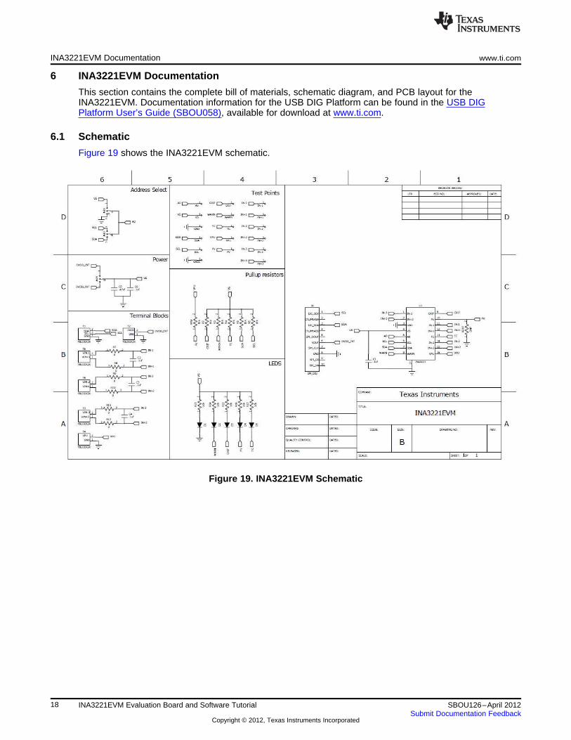
6 INA3221EVM Documentation
This section contains the complete bill of materials, schematic diagram, and PCB layout for theINA3221EVM. Documentation information for the USB DIG Platform can be found in the USB DIGPlatform User’s Guide (SBOU058), available for download at www.ti.com.
6.1 Schematic
Figure 19 shows the INA3221EVM schematic.
Figure 19. INA3221EVM Schematic
18 INA3221EVM Evaluation Board and Software Tutorial SBOU126–April 2012Submit Documentation Feedback
Copyright © 2012, Texas Instruments Incorporated

www.ti.com INA3221EVM Documentation
6.2 PCB Layout
Figure 20 shows the INA3221EVM PCB component layout.
Figure 20. INA3221EVM PCB Top Layer (Component Side)
19SBOU126–April 2012 INA3221EVM Evaluation Board and Software TutorialSubmit Documentation Feedback
Copyright © 2012, Texas Instruments Incorporated
INA3221EVM Documentation www.ti.com
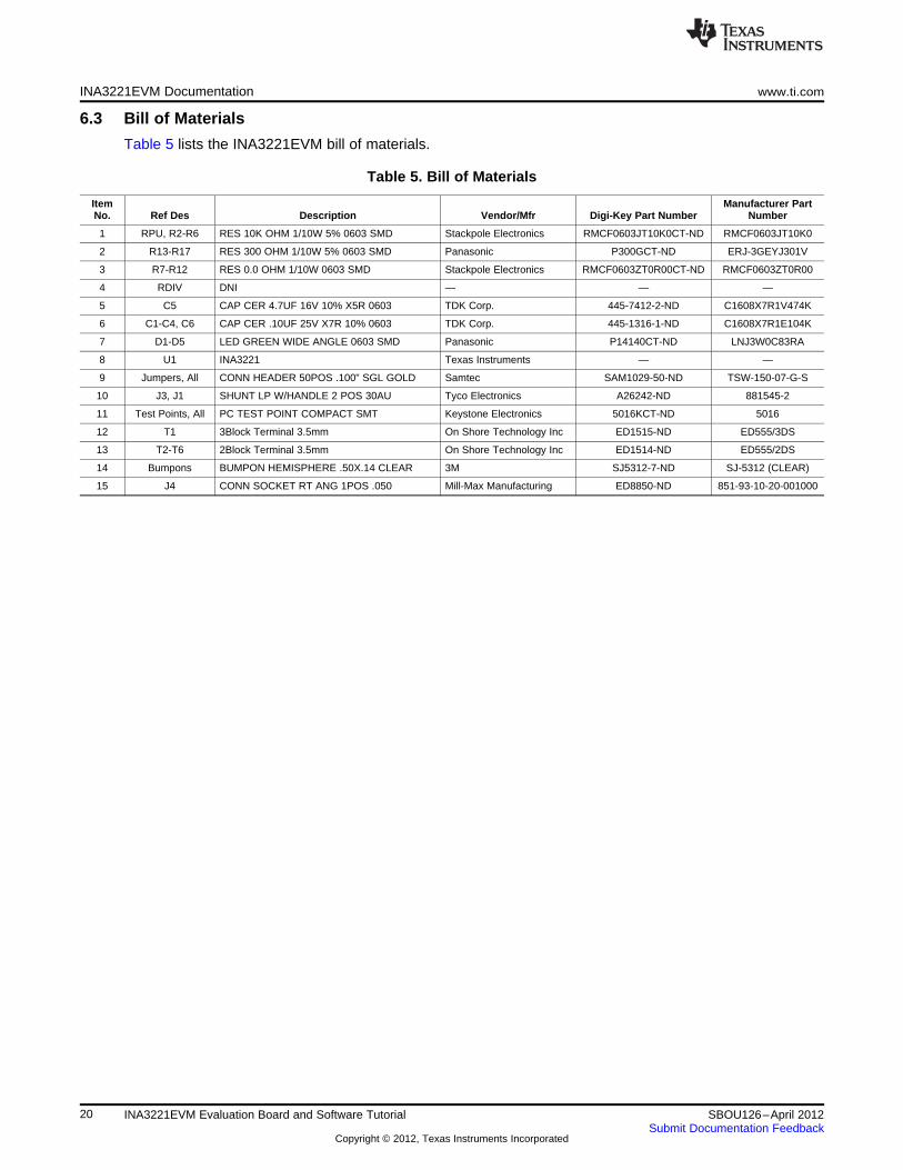
6.3 Bill of Materials
Table 5 lists the INA3221EVM bill of materials.
Table 5. Bill of Materials
Item Manufacturer PartNo. Ref Des Description Vendor/Mfr Digi-Key Part Number Number
1 RPU, R2-R6 RES 10K OHM 1/10W 5% 0603 SMD Stackpole Electronics RMCF0603JT10K0CT-ND RMCF0603JT10K0
2 R13-R17 RES 300 OHM 1/10W 5% 0603 SMD Panasonic P300GCT-ND ERJ-3GEYJ301V
3 R7-R12 RES 0.0 OHM 1/10W 0603 SMD Stackpole Electronics RMCF0603ZT0R00CT-ND RMCF0603ZT0R00
4 RDIV DNI — — —
5 C5 CAP CER 4.7UF 16V 10% X5R 0603 TDK Corp. 445-7412-2-ND C1608X7R1V474K
6 C1-C4, C6 CAP CER .10UF 25V X7R 10% 0603 TDK Corp. 445-1316-1-ND C1608X7R1E104K
7 D1-D5 LED GREEN WIDE ANGLE 0603 SMD Panasonic P14140CT-ND LNJ3W0C83RA
8 U1 INA3221 Texas Instruments — —
9 Jumpers, All CONN HEADER 50POS .100" SGL GOLD Samtec SAM1029-50-ND TSW-150-07-G-S
10 J3, J1 SHUNT LP W/HANDLE 2 POS 30AU Tyco Electronics A26242-ND 881545-2
11 Test Points, All PC TEST POINT COMPACT SMT Keystone Electronics 5016KCT-ND 5016
12 T1 3Block Terminal 3.5mm On Shore Technology Inc ED1515-ND ED555/3DS
13 T2-T6 2Block Terminal 3.5mm On Shore Technology Inc ED1514-ND ED555/2DS
14 Bumpons BUMPON HEMISPHERE .50X.14 CLEAR 3M SJ5312-7-ND SJ-5312 (CLEAR)
15 J4 CONN SOCKET RT ANG 1POS .050 Mill-Max Manufacturing ED8850-ND 851-93-10-20-001000
20 INA3221EVM Evaluation Board and Software Tutorial SBOU126–April 2012Submit Documentation Feedback
Copyright © 2012, Texas Instruments Incorporated
Evaluation Board/Kit Important Notice
Texas Instruments (TI) provides the enclosed product(s) under the following conditions:
This evaluation board/kit is intended for use for ENGINEERING DEVELOPMENT, DEMONSTRATION, OR EVALUATION PURPOSESONLY and is not considered by TI to be a finished end-product fit for general consumer use. Persons handling the product(s) must haveelectronics training and observe good engineering practice standards. As such, the goods being provided are not intended to be completein terms of required design-, marketing-, and/or manufacturing-related protective considerations, including product safety and environmentalmeasures typically found in end products that incorporate such semiconductor components or circuit boards. This evaluation board/kit doesnot fall within the scope of the European Union directives regarding electromagnetic compatibility, restricted substances (RoHS), recycling(WEEE), FCC, CE or UL, and therefore may not meet the technical requirements of these directives or other related directives.
Should this evaluation board/kit not meet the specifications indicated in the User’s Guide, the board/kit may be returned within 30 days fromthe date of delivery for a full refund. THE FOREGOING WARRANTY IS THE EXCLUSIVE WARRANTY MADE BY SELLER TO BUYERAND IS IN LIEU OF ALL OTHER WARRANTIES, EXPRESSED, IMPLIED, OR STATUTORY, INCLUDING ANY WARRANTY OFMERCHANTABILITY OR FITNESS FOR ANY PARTICULAR PURPOSE.
The user assumes all responsibility and liability for proper and safe handling of the goods. Further, the user indemnifies TI from all claimsarising from the handling or use of the goods. Due to the open construction of the product, it is the user’s responsibility to take any and allappropriate precautions with regard to electrostatic discharge.
EXCEPT TO THE EXTENT OF THE INDEMNITY SET FORTH ABOVE, NEITHER PARTY SHALL BE LIABLE TO THE OTHER FOR ANYINDIRECT, SPECIAL, INCIDENTAL, OR CONSEQUENTIAL DAMAGES.
TI currently deals with a variety of customers for products, and therefore our arrangement with the user is not exclusive.
TI assumes no liability for applications assistance, customer product design, software performance, or infringement of patents orservices described herein.
Please read the User’s Guide and, specifically, the Warnings and Restrictions notice in the User’s Guide prior to handling the product. Thisnotice contains important safety information about temperatures and voltages. For additional information on TI’s environmental and/orsafety programs, please contact the TI application engineer or visit www.ti.com/esh.
No license is granted under any patent right or other intellectual property right of TI covering or relating to any machine, process, orcombination in which such TI products or services might be or are used.
FCC Warning
This evaluation board/kit is intended for use for ENGINEERING DEVELOPMENT, DEMONSTRATION, OR EVALUATION PURPOSESONLY and is not considered by TI to be a finished end-product fit for general consumer use. It generates, uses, and can radiate radiofrequency energy and has not been tested for compliance with the limits of computing devices pursuant to part 15 of FCC rules, which aredesigned to provide reasonable protection against radio frequency interference. Operation of this equipment in other environments maycause interference with radio communications, in which case the user at his own expense will be required to take whatever measures maybe required to correct this interference.
EVM Warnings and Restrictions
It is important to operate this EVM within the input voltage range of 0 V to 26 V and the output voltage range of 2.7 V to 5.5 V.
Exceeding the specified input range may cause unexpected operation and/or irreversible damage to the EVM. If there are questionsconcerning the input range, please contact a TI field representative prior to connecting the input power.
Applying loads outside of the specified output range may result in unintended operation and/or possible permanent damage to the EVM.Please consult the EVM User's Guide prior to connecting any load to the EVM output. If there is uncertainty as to the load specification,please contact a TI field representative.
During normal operation, some circuit components may have case temperatures greater than +25°C. The EVM is designed to operateproperly with certain components above +25°C as long as the input and output ranges are maintained. These components include but arenot limited to linear regulators, switching transistors, pass transistors, and current sense resistors. These types of devices can be identifiedusing the EVM schematic located in the EVM User's Guide. When placing measurement probes near these devices during operation,please be aware that these devices may be very warm to the touch.
Mailing Address: Texas Instruments, Post Office Box 655303, Dallas, Texas 75265Copyright © 2012, Texas Instruments Incorporated
EVALUATION BOARD/KIT/MODULE (EVM) ADDITIONAL TERMSTexas Instruments (TI) provides the enclosed Evaluation Board/Kit/Module (EVM) under the following conditions:
The user assumes all responsibility and liability for proper and safe handling of the goods. Further, the user indemnifies TI from all claimsarising from the handling or use of the goods.
Should this evaluation board/kit not meet the specifications indicated in the User’s Guide, the board/kit may be returned within 30 days fromthe date of delivery for a full refund. THE FOREGOING LIMITED WARRANTY IS THE EXCLUSIVE WARRANTY MADE BY SELLER TOBUYER AND IS IN LIEU OF ALL OTHER WARRANTIES, EXPRESSED, IMPLIED, OR STATUTORY, INCLUDING ANY WARRANTY OFMERCHANTABILITY OR FITNESS FOR ANY PARTICULAR PURPOSE. EXCEPT TO THE EXTENT OF THE INDEMNITY SET FORTHABOVE, NEITHER PARTY SHALL BE LIABLE TO THE OTHER FOR ANY INDIRECT, SPECIAL, INCIDENTAL, OR CONSEQUENTIALDAMAGES.
Please read the User's Guide and, specifically, the Warnings and Restrictions notice in the User's Guide prior to handling the product. Thisnotice contains important safety information about temperatures and voltages. For additional information on TI's environmental and/or safetyprograms, please visit www.ti.com/esh or contact TI.
No license is granted under any patent right or other intellectual property right of TI covering or relating to any machine, process, orcombination in which such TI products or services might be or are used. TI currently deals with a variety of customers for products, andtherefore our arrangement with the user is not exclusive. TI assumes no liability for applications assistance, customer product design,software performance, or infringement of patents or services described herein.
REGULATORY COMPLIANCE INFORMATIONAs noted in the EVM User’s Guide and/or EVM itself, this EVM and/or accompanying hardware may or may not be subject to the FederalCommunications Commission (FCC) and Industry Canada (IC) rules.
For EVMs not subject to the above rules, this evaluation board/kit/module is intended for use for ENGINEERING DEVELOPMENT,DEMONSTRATION OR EVALUATION PURPOSES ONLY and is not considered by TI to be a finished end product fit for general consumeruse. It generates, uses, and can radiate radio frequency energy and has not been tested for compliance with the limits of computingdevices pursuant to part 15 of FCC or ICES-003 rules, which are designed to provide reasonable protection against radio frequencyinterference. Operation of the equipment may cause interference with radio communications, in which case the user at his own expense willbe required to take whatever measures may be required to correct this interference.
General Statement for EVMs including a radioUser Power/Frequency Use Obligations: This radio is intended for development/professional use only in legally allocated frequency andpower limits. Any use of radio frequencies and/or power availability of this EVM and its development application(s) must comply with locallaws governing radio spectrum allocation and power limits for this evaluation module. It is the user’s sole responsibility to only operate thisradio in legally acceptable frequency space and within legally mandated power limitations. Any exceptions to this are strictly prohibited andunauthorized by Texas Instruments unless user has obtained appropriate experimental/development licenses from local regulatoryauthorities, which is responsibility of user including its acceptable authorization.
For EVMs annotated as FCC – FEDERAL COMMUNICATIONS COMMISSION Part 15 Compliant
CautionThis device complies with part 15 of the FCC Rules. Operation is subject to the following two conditions: (1) This device may not causeharmful interference, and (2) this device must accept any interference received, including interference that may cause undesired operation.
Changes or modifications not expressly approved by the party responsible for compliance could void the user's authority to operate theequipment.
FCC Interference Statement for Class A EVM devicesThis equipment has been tested and found to comply with the limits for a Class A digital device, pursuant to part 15 of the FCC Rules.These limits are designed to provide reasonable protection against harmful interference when the equipment is operated in a commercialenvironment. This equipment generates, uses, and can radiate radio frequency energy and, if not installed and used in accordance with theinstruction manual, may cause harmful interference to radio communications. Operation of this equipment in a residential area is likely tocause harmful interference in which case the user will be required to correct the interference at his own expense.
FCC Interference Statement for Class B EVM devicesThis equipment has been tested and found to comply with the limits for a Class B digital device, pursuant to part 15 of the FCC Rules.These limits are designed to provide reasonable protection against harmful interference in a residential installation. This equipmentgenerates, uses and can radiate radio frequency energy and, if not installed and used in accordance with the instructions, may causeharmful interference to radio communications. However, there is no guarantee that interference will not occur in a particular installation. Ifthis equipment does cause harmful interference to radio or television reception, which can be determined by turning the equipment off andon, the user is encouraged to try to correct the interference by one or more of the following measures:
• Reorient or relocate the receiving antenna.• Increase the separation between the equipment and receiver.• Connect the equipment into an outlet on a circuit different from that to which the receiver is connected.• Consult the dealer or an experienced radio/TV technician for help.
For EVMs annotated as IC – INDUSTRY CANADA Compliant
This Class A or B digital apparatus complies with Canadian ICES-003.
Changes or modifications not expressly approved by the party responsible for compliance could void the user’s authority to operate theequipment.
Concerning EVMs including radio transmitters
This device complies with Industry Canada licence-exempt RSS standard(s). Operation is subject to the following two conditions: (1) thisdevice may not cause interference, and (2) this device must accept any interference, including interference that may cause undesiredoperation of the device.
Concerning EVMs including detachable antennasUnder Industry Canada regulations, this radio transmitter may only operate using an antenna of a type and maximum (or lesser) gainapproved for the transmitter by Industry Canada. To reduce potential radio interference to other users, the antenna type and its gain shouldbe so chosen that the equivalent isotropically radiated power (e.i.r.p.) is not more than that necessary for successful communication.
This radio transmitter has been approved by Industry Canada to operate with the antenna types listed in the user guide with the maximumpermissible gain and required antenna impedance for each antenna type indicated. Antenna types not included in this list, having a gaingreater than the maximum gain indicated for that type, are strictly prohibited for use with this device.
Cet appareil numérique de la classe A ou B est conforme à la norme NMB-003 du Canada.
Les changements ou les modifications pas expressément approuvés par la partie responsable de la conformité ont pu vider l’autorité del'utilisateur pour actionner l'équipement.
Concernant les EVMs avec appareils radio
Le présent appareil est conforme aux CNR d'Industrie Canada applicables aux appareils radio exempts de licence. L'exploitation estautorisée aux deux conditions suivantes : (1) l'appareil ne doit pas produire de brouillage, et (2) l'utilisateur de l'appareil doit accepter toutbrouillage radioélectrique subi, même si le brouillage est susceptible d'en compromettre le fonctionnement.
Concernant les EVMs avec antennes détachables
Conformément à la réglementation d'Industrie Canada, le présent émetteur radio peut fonctionner avec une antenne d'un type et d'un gainmaximal (ou inférieur) approuvé pour l'émetteur par Industrie Canada. Dans le but de réduire les risques de brouillage radioélectrique àl'intention des autres utilisateurs, il faut choisir le type d'antenne et son gain de sorte que la puissance isotrope rayonnée équivalente(p.i.r.e.) ne dépasse pas l'intensité nécessaire à l'établissement d'une communication satisfaisante.
Le présent émetteur radio a été approuvé par Industrie Canada pour fonctionner avec les types d'antenne énumérés dans le manueld’usage et ayant un gain admissible maximal et l'impédance requise pour chaque type d'antenne. Les types d'antenne non inclus danscette liste, ou dont le gain est supérieur au gain maximal indiqué, sont strictement interdits pour l'exploitation de l'émetteur.
SPACER
SPACER
SPACER
SPACER
SPACER
SPACER
SPACER
SPACER

【【Important Notice for Users of this Product in Japan】】This development kit is NOT certified as Confirming to Technical Regulations of Radio Law of Japan
If you use this product in Japan, you are required by Radio Law of Japan to follow the instructions below with respect to this product:
1. Use this product in a shielded room or any other test facility as defined in the notification #173 issued by Ministry of Internal Affairs andCommunications on March 28, 2006, based on Sub-section 1.1 of Article 6 of the Ministry’s Rule for Enforcement of Radio Law ofJapan,
2. Use this product only after you obtained the license of Test Radio Station as provided in Radio Law of Japan with respect to thisproduct, or
3. Use of this product only after you obtained the Technical Regulations Conformity Certification as provided in Radio Law of Japan withrespect to this product. Also, please do not transfer this product, unless you give the same notice above to the transferee. Please notethat if you could not follow the instructions above, you will be subject to penalties of Radio Law of Japan.
Texas Instruments Japan Limited(address) 24-1, Nishi-Shinjuku 6 chome, Shinjuku-ku, Tokyo, Japan
http://www.tij.co.jp
【ご使用にあたっての注】
本開発キットは技術基準適合証明を受けておりません。
本製品のご使用に際しては、電波法遵守のため、以下のいずれかの措置を取っていただく必要がありますのでご注意ください。1. 電波法施行規則第6条第1項第1号に基づく平成18年3月28日総務省告示第173号で定められた電波暗室等の試験設備でご使用いただく。2. 実験局の免許を取得後ご使用いただく。3. 技術基準適合証明を取得後ご使用いただく。
なお、本製品は、上記の「ご使用にあたっての注意」を譲渡先、移転先に通知しない限り、譲渡、移転できないものとします。
上記を遵守頂けない場合は、電波法の罰則が適用される可能性があることをご留意ください。
日本テキサス・インスツルメンツ株式会社東京都新宿区西新宿6丁目24番1号西新宿三井ビルhttp://www.tij.co.jp
SPACER
SPACER
SPACER
SPACER
SPACER
SPACER
SPACER
SPACER
SPACER
SPACER
SPACER
SPACER
SPACER
SPACER
SPACER
SPACER
EVALUATION BOARD/KIT/MODULE (EVM)WARNINGS, RESTRICTIONS AND DISCLAIMERS
For Feasibility Evaluation Only, in Laboratory/Development Environments. Unless otherwise indicated, this EVM is not a finishedelectrical equipment and not intended for consumer use. It is intended solely for use for preliminary feasibility evaluation inlaboratory/development environments by technically qualified electronics experts who are familiar with the dangers and application risksassociated with handling electrical mechanical components, systems and subsystems. It should not be used as all or part of a finished endproduct.
Your Sole Responsibility and Risk. You acknowledge, represent and agree that:
1. You have unique knowledge concerning Federal, State and local regulatory requirements (including but not limited to Food and DrugAdministration regulations, if applicable) which relate to your products and which relate to your use (and/or that of your employees,affiliates, contractors or designees) of the EVM for evaluation, testing and other purposes.
2. You have full and exclusive responsibility to assure the safety and compliance of your products with all such laws and other applicableregulatory requirements, and also to assure the safety of any activities to be conducted by you and/or your employees, affiliates,contractors or designees, using the EVM. Further, you are responsible to assure that any interfaces (electronic and/or mechanical)between the EVM and any human body are designed with suitable isolation and means to safely limit accessible leakage currents tominimize the risk of electrical shock hazard.
3. You will employ reasonable safeguards to ensure that your use of the EVM will not result in any property damage, injury or death, evenif the EVM should fail to perform as described or expected.
4. You will take care of proper disposal and recycling of the EVM’s electronic components and packing materials.
Certain Instructions. It is important to operate this EVM within TI’s recommended specifications and environmental considerations per theuser guidelines. Exceeding the specified EVM ratings (including but not limited to input and output voltage, current, power, andenvironmental ranges) may cause property damage, personal injury or death. If there are questions concerning these ratings please contacta TI field representative prior to connecting interface electronics including input power and intended loads. Any loads applied outside of thespecified output range may result in unintended and/or inaccurate operation and/or possible permanent damage to the EVM and/orinterface electronics. Please consult the EVM User's Guide prior to connecting any load to the EVM output. If there is uncertainty as to theload specification, please contact a TI field representative. During normal operation, some circuit components may have case temperaturesgreater than 60°C as long as the input and output are maintained at a normal ambient operating temperature. These components includebut are not limited to linear regulators, switching transistors, pass transistors, and current sense resistors which can be identified using theEVM schematic located in the EVM User's Guide. When placing measurement probes near these devices during normal operation, pleasebe aware that these devices may be very warm to the touch. As with all electronic evaluation tools, only qualified personnel knowledgeablein electronic measurement and diagnostics normally found in development environments should use these EVMs.
Agreement to Defend, Indemnify and Hold Harmless. You agree to defend, indemnify and hold TI, its licensors and their representativesharmless from and against any and all claims, damages, losses, expenses, costs and liabilities (collectively, "Claims") arising out of or inconnection with any use of the EVM that is not in accordance with the terms of the agreement. This obligation shall apply whether Claimsarise under law of tort or contract or any other legal theory, and even if the EVM fails to perform as described or expected.
Safety-Critical or Life-Critical Applications. If you intend to evaluate the components for possible use in safety critical applications (suchas life support) where a failure of the TI product would reasonably be expected to cause severe personal injury or death, such as deviceswhich are classified as FDA Class III or similar classification, then you must specifically notify TI of such intent and enter into a separateAssurance and Indemnity Agreement.
Mailing Address: Texas Instruments, Post Office Box 655303, Dallas, Texas 75265Copyright © 2012, Texas Instruments Incorporated

IMPORTANT NOTICE
Texas Instruments Incorporated and its subsidiaries (TI) reserve the right to make corrections, enhancements, improvements and otherchanges to its semiconductor products and services per JESD46, latest issue, and to discontinue any product or service per JESD48, latestissue. Buyers should obtain the latest relevant information before placing orders and should verify that such information is current andcomplete. All semiconductor products (also referred to herein as “components”) are sold subject to TI’s terms and conditions of salesupplied at the time of order acknowledgment.
TI warrants performance of its components to the specifications applicable at the time of sale, in accordance with the warranty in TI’s termsand conditions of sale of semiconductor products. Testing and other quality control techniques are used to the extent TI deems necessaryto support this warranty. Except where mandated by applicable law, testing of all parameters of each component is not necessarilyperformed.
TI assumes no liability for applications assistance or the design of Buyers’ products. Buyers are responsible for their products andapplications using TI components. To minimize the risks associated with Buyers’ products and applications, Buyers should provideadequate design and operating safeguards.
TI does not warrant or represent that any license, either express or implied, is granted under any patent right, copyright, mask work right, orother intellectual property right relating to any combination, machine, or process in which TI components or services are used. Informationpublished by TI regarding third-party products or services does not constitute a license to use such products or services or a warranty orendorsement thereof. Use of such information may require a license from a third party under the patents or other intellectual property of thethird party, or a license from TI under the patents or other intellectual property of TI.
Reproduction of significant portions of TI information in TI data books or data sheets is permissible only if reproduction is without alterationand is accompanied by all associated warranties, conditions, limitations, and notices. TI is not responsible or liable for such altereddocumentation. Information of third parties may be subject to additional restrictions.
Resale of TI components or services with statements different from or beyond the parameters stated by TI for that component or servicevoids all express and any implied warranties for the associated TI component or service and is an unfair and deceptive business practice.TI is not responsible or liable for any such statements.
Buyer acknowledges and agrees that it is solely responsible for compliance with all legal, regulatory and safety-related requirementsconcerning its products, and any use of TI components in its applications, notwithstanding any applications-related information or supportthat may be provided by TI. Buyer represents and agrees that it has all the necessary expertise to create and implement safeguards whichanticipate dangerous consequences of failures, monitor failures and their consequences, lessen the likelihood of failures that might causeharm and take appropriate remedial actions. Buyer will fully indemnify TI and its representatives against any damages arising out of the useof any TI components in safety-critical applications.
In some cases, TI components may be promoted specifically to facilitate safety-related applications. With such components, TI’s goal is tohelp enable customers to design and create their own end-product solutions that meet applicable functional safety standards andrequirements. Nonetheless, such components are subject to these terms.
No TI components are authorized for use in FDA Class III (or similar life-critical medical equipment) unless authorized officers of the partieshave executed a special agreement specifically governing such use.
Only those TI components which TI has specifically designated as military grade or “enhanced plastic” are designed and intended for use inmilitary/aerospace applications or environments. Buyer acknowledges and agrees that any military or aerospace use of TI componentswhich have not been so designated is solely at the Buyer's risk, and that Buyer is solely responsible for compliance with all legal andregulatory requirements in connection with such use.
TI has specifically designated certain components which meet ISO/TS16949 requirements, mainly for automotive use. Components whichhave not been so designated are neither designed nor intended for automotive use; and TI will not be responsible for any failure of suchcomponents to meet such requirements.
Products Applications
Audio www.ti.com/audio Automotive and Transportation www.ti.com/automotive
Amplifiers amplifier.ti.com Communications and Telecom www.ti.com/communications
Data Converters dataconverter.ti.com Computers and Peripherals www.ti.com/computers
DLP® Products www.dlp.com Consumer Electronics www.ti.com/consumer-apps
DSP dsp.ti.com Energy and Lighting www.ti.com/energy
Clocks and Timers www.ti.com/clocks Industrial www.ti.com/industrial
Interface interface.ti.com Medical www.ti.com/medical
Logic logic.ti.com Security www.ti.com/security
Power Mgmt power.ti.com Space, Avionics and Defense www.ti.com/space-avionics-defense
Microcontrollers microcontroller.ti.com Video and Imaging www.ti.com/video
RFID www.ti-rfid.com
OMAP Applications Processors www.ti.com/omap TI E2E Community e2e.ti.com
Wireless Connectivity www.ti.com/wirelessconnectivity
Mailing Address: Texas Instruments, Post Office Box 655303, Dallas, Texas 75265Copyright © 2012, Texas Instruments Incorporated
![AK7734 Evaluation Board Rev - AKM Evaluation Board Rev.1 AKD7734-A [AKD7734-A] 2011/07 - 2 - Evaluation Board Diagram Board Diagram +12V-12V](https://img.pdfslide.net/doc/110x75/5c03e45309d3f203258d6861/ak7734-evaluation-board-rev-akm-evaluation-board-rev1-akd7734-a-akd7734-a-201107.jpg)