Embed Size (px)
Citation preview

Specifications are subject to change without any obligation on the part of the manufacturer.
Illumination devices for microscope have suggested lifetimes. Periodic inspections are required. Visit our Website for details.
OLYMPUS CORPORATION has obtained ISO9001/ISO14001
INFRARED MICROSCOPE SYSTEMFOR SILICON INTERIOR INSPECTION
Printed in Japan M1585E-0408B
Class 1 laser product: OLS3000-IR only
1
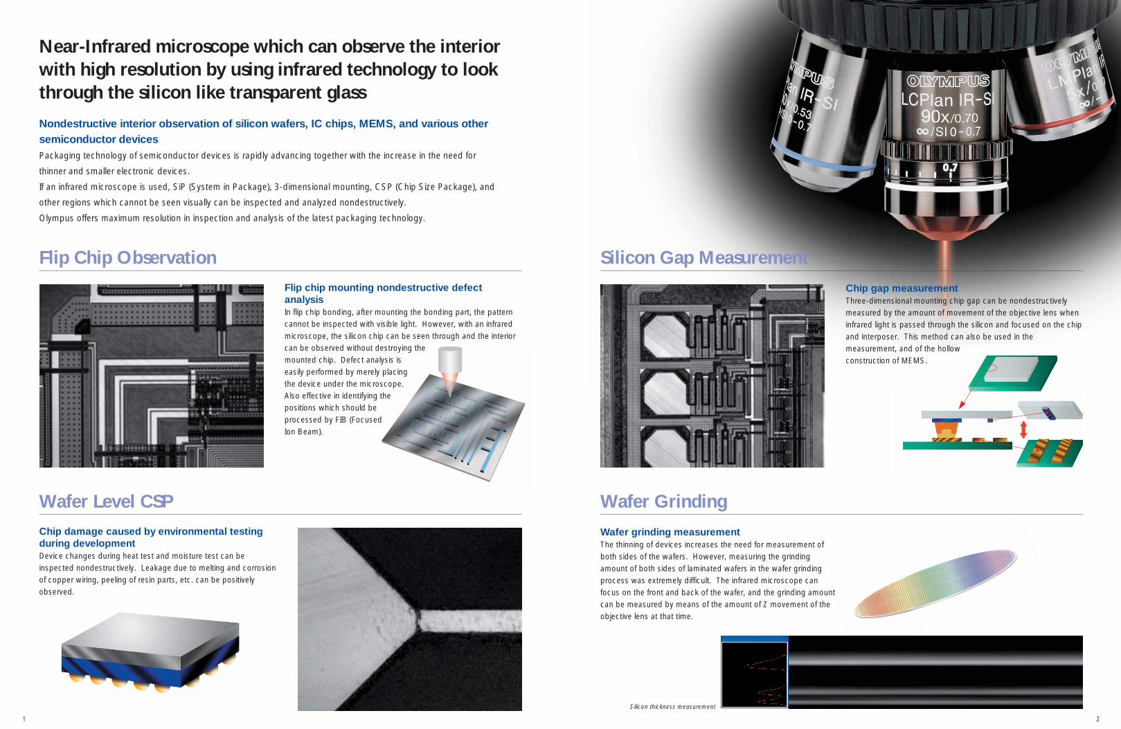
Near-Infrared microscope which can observe the interiorwith high resolution by using infrared technology to lookthrough the silicon like transparent glass
Flip chip mounting nondestructive defectanalysisIn flip chip bonding, after mounting the bonding part, the patterncannot be inspected with visible light. However, with an infraredmicroscope, the silicon chip can be seen through and the interiorcan be observed without destroying themounted chip. Defect analysis iseasily performed by merely placingthe device under the microscope.Also effective in identifying thepositions which should beprocessed by FIB (FocusedIon Beam).
Chip damage caused by environmental testingduring developmentDevice changes during heat test and moisture test can beinspected nondestructively. Leakage due to melting and corrosionof copper wiring, peeling of resin parts, etc. can be positivelyobserved.
Wafer Level CSP
Nondestructive interior observation of silicon wafers, IC chips, MEMS, and various othersemiconductor devicesPackaging technology of semiconductor devices is rapidly advancing together with the increase in the need for
thinner and smaller electronic devices.
If an infrared microscope is used, SiP (System in Package), 3-dimensional mounting, CSP (Chip Size Package), and
other regions which cannot be seen visually can be inspected and analyzed nondestructively.
Olympus offers maximum resolution in inspection and analysis of the latest packaging technology.
Flip Chip Observation
Wafer grinding measurementThe thinning of devices increases the need for measurement ofboth sides of the wafers. However, measuring the grindingamount of both sides of laminated wafers in the wafer grindingprocess was extremely difficult. The infrared microscope canfocus on the front and back of the wafer, and the grinding amountcan be measured by means of the amount of Z movement of theobjective lens at that time.
Silicon Gap Measurement
Wafer Grinding
Silicon thickness measurement
2
Chip gap measurementThree-dimensional mounting chip gap can be nondestructivelymeasured by the amount of movement of the objective lens wheninfrared light is passed through the silicon and focused on the chipand interposer. This method can also be used in themeasurement, and of the hollowconstruction of MEMS.

Interior of IC invisible with visible light is observed atan incredibly high resolution
•High resolution near infrared microscopic observation is possible by highpower IR laser and confocal optical systemResolution of 0.55µm line and space pattern
•High precision nondestructive measurement of MEMS gap and siliconthickness by nondestructive height measurement functionZ measurement accuracy: 3σ n-1=0.10+0.002L µm or lessL=Measurement range (units: µm)
MX series•Compatible with 150-200 mm wafers
•Superior operability increases semiconductor scanning efficiency
•Motorized revolving nosepiece switches objective lens to direct
•SEMI S2/S8 compliance and high safety and ergonomic propertiessecured
MX61 MX51
BX2M series•General purpose standard type which also allows transmitted nearinfrared microscopic observation
•UIS optical system with the world’s highest level of optical performance
•Y shaped design with advanced ergonomics
BX51 BX51M50x image 90x image
Confocal IR laser scanningmicroscope
OLS3000-IRTM
System industrialmicroscopes
BX2M series
Semiconductor inspectionmicroscopes
MX series
OLS3000-IR optical systemPhotodiode
Confocal opticswith circularpinhole
Objective lenses
Laser
3 4
BX61
Line up of near infrared microscopes that pursuehigh operability and cost-performance
5 6
Modular optical unit compatible with infraredobservation
ø3216
9
19~49
124
84208
29020
4045
106 187
92.5
Specimen surface
Infrared region compatiblemodular optical unit
BXFM
•Optimal U-KMAS reflected light illumination for BF built into theequipment is installed.
•Motorized revolving nosepieces, 100W halogen lamp housing for IR,TH4-100/200 external light sources and other units which allowexternal control are available.
•UIS optical system without any magnification changes or objectdegradation even when the distance between the objective lens andtube lens changes.
Specifications
✓ ✓ ✓ ✓OLS3000-IR
MX61 ✓ ✓ ✓ Wafer compatible
MX51 ✓ ✓ Wafer compatible
BX61 ✓ ✓ ✓
BX51 ✓ ✓
BX51M ✓ Standard
BXFM-S ✓ Equipment oriented
TM
Infraredconfocal
observation
Infraredreflected lightobservation
Infraredtransmitted
lightobservation
Z measure-ment
200mm wafer
compatibility
Motorizedoperation
High resolutionobservation/
high precisionmeasurement
Transmitted light observation
Transmitted lightobservation
Model Appearance Features
■ OthersExternal light sources/ TH4-100/200Hand switch/ TH4-HSReflected polarizer slider for IR/ U-POIRRotatable analyzer slider for IR/ U-AN360IRBand path filter (1100nm) for IR/ U-BP1100IRBand path filter (1200nm) for IR/ U-BP1200IR
■ Observation tubes
■ Lamp housing
Trinocular tube for IRU-TR30NIR
Single port tube with lens for IRU-TLUIR
100W halogen lamp housing for IRU-LH100IR
■ UIS optical system infrared dedicated objective lenses
ø26
(26.
5)W
D=
18.5
454.
5
(36.
9)
ø20.32 ø20.32
ø26
4545W
D=
20(2
5)
ø20.32
WD
=8.
1ø26
4.5
454.
5
ø20.32
ø26
(39)
WD
=6
4.5
ø20.32
(43.
43)
WD
=1.
1 ø29ø31
45.2
38
107
135146.5
85.5
37
64.5
43.5188.9
93.9
95.8
ø60
58
4.5
ø20.32
(43.
43)
WD
=1.
1 ø29ø31
45.2
38
(44.
7)
4.5
45
WD
=0.
3
ø20.32
454.
5
ø20.32
45
ø26ø26
(39)
WD
=6
4.7
ø20.32
(41.
6)W
D=
3.4ø26
LMPL5xIR
LMPL50xIR LMPL100xIR MPL100xIR
LMPL10xIR LMPL20xIR LMPL50xIR-Si LCPL90xIR-Si
(Units: mm)(Units: mm)
(Units: mm)
Objective lenses Numerical Working RemarksAperture Distance (mm)
LMPL5xIR 0.10 20.00LMPL10xIR 0.25 18.50LMPL20xIR 0.40 8.10LMPL50xIR 0.55 6.00LMPL100xIR 0.80 3.40MPL100xIR 0.95 0.30LMPL50xIR-Si 0.53 6.00 Correction for silicon/LCPL90xIR-Si 0.70 1.2~0.7 Exclusive for OLS3000-IR