Embed Size (px)
Citation preview

ORIGINAL ARTICLE
Investigation of the cutoff frequency of double linear halo lightlydoped drain and source CNTFET
Mohammad Javad Hejazifar • Seyed Ali Sedigh Ziabari
Received: 12 February 2014 / Accepted: 2 August 2014 / Published online: 26 August 2014
� The Author(s) 2014. This article is published with open access at Springerlink.com
Abstract In this work we investigate the n-type single
halo implantation in channel of lightly doped drain and
source CNTFET (SH-LDDS-CNTFET) and propose the
n-type double linear halo implantation in the channel of
LDDS-CNTFET. These transistors are simulated with a
non-equilibrium Green’s function method. We demonstrate
that in the proposed structure the fT at the VGS ranges of
0–0.25 V and more than 0.42 V is much higher compared
to the LDDS-CNTFET and SH-LDDS-CNTFET and the
SH-LDDS-CNTFET, respectively. Finally, simulations
demonstrate that the fT of the proposed transistor is more
than the LDDS-CNTFET at a wide range of VGS, whereas
the fT of SH-LDDS-CNTFET is more than the LDDS-
CNTFET for narrow ranges of VGS.
Keywords Carbon nanotube field effect transistor
(CNTFET) � Cutoff frequency (fT) � Single halo (SH) �Double linear halo (DLH) � Non-equilibrium Green’s
function (NEGF)
Introduction
After discovering the carbon nanotube (CNT) by Aijima [1],
scientific researches about this structure are expanded due to
its excellent electronic properties. One of the important
properties of this structure is quasi-ballistic transport with
very high carrier mobility [2, 3]. Using carbon nanotube, two
types of field effect transistors have been discussed. The first
type is Schottky barrier carbon nanotube field effect transistor
(SB-CNTFET) and second type is MOSFET-like CNTFETs
(MOSCNTs). The MOSCNT was more favorable because of
the high on–off current ratio, but leakage current (IL) of this
transistor is very high because of electron band-to-band tun-
neling (BTBT) [4]. In order to deal with this problem, some
solutions such as drain and source with a linearly or lightly
doped, source and drain extensions and asymmetric oxide
thickness, have been proposed [5–9]. Also, the dual material
gate structure and the source and drain parameters effect on
the characteristics of CNTFET are investigated [10, 11].
Moreover the p-type halo implanted deteriorates the cutoff
frequency and the switching delay of CNTFET [12].
This paper is mainly focused on the fT of MOSCNT,
linearly doped CNTFET (LD-CNTFET) and lightly doped
drain and source CNTFET (LDDS-CNTFET), which are
discussed in [7], to select a structure with the highest fT.
Moreover, we have investigated the implantation of n-type
single halo in channel of LDDS-CNTFET (SH-LDDS-
CNTFET) and its effects on some characteristics such as
the fT. Based on this investigation we have proposed
implanting n-type double linear halo in the channel of
LDDS-CNTFET which is named ‘‘DLH-LDDS-CNT-
FET’’. These structure characteristics such as the leakage
current, the on-current and the fT have been investigated.
We have used a non-equilibrium Green’s function (NEGF)
method to simulate these transistors [8, 13–17].
M. J. Hejazifar
Department of Electrical Engineering, Guilan Science and
Research Branch, Islamic Azad University, Guilan, Iran
e-mail: [email protected]
S. A. Sedigh Ziabari (&)
Department of Electrical Engineering, Roudbar Branch, Islamic
Azad University, Roudbar, Iran
e-mail: [email protected]
123
Int Nano Lett (2014) 4:118
DOI 10.1007/s40089-014-0118-3

Proposed transistor and method of simulation
A cross-section schematic representation of implanting the
n-type single halo in the source side of channel of LDDS-
CNTFET and their geometric details is shown in Fig. 1a.
The channel is a (16, 0) CNT and radius 0.63 nm that is
embedded in cylindrical gate insulator of HfO2 with
thickness 2 nm and dielectric constant 16. The channel
length is 15 nm, which consists of 9 nm undoped CNT and
6 nm n-type doped CNT. The concentration of this single
halo is 1.4 nm-1. Our proposed structure is shown in
Fig. 1b. This figure illustrates a cross-section schematic
representation of the n-type double linear halo implantation
in the channel of LDDS-CNTFET (DLH-LDDS-CNTFET)
and their detailed geometries. The drain and source length
are 30 nm, which consists of 15 nm highly doped regions
and 15 nm lightly doped regions are taken to be 2 and
0.2 nm-1, respectively. Figure 1b also shows that the
concentration of n-type double linear halo vary from
1.4 nm-1 to 0 in length of 6 nm.
Self consistent solution of the Poisson and Schrodinger
equations has been done within the NEGF formalism for
simulating the device characteristics. The band structure of
CNT is calculated by the tight-binding method with one
orbital. The electrostatic potential of CNT required for
calculating the Hamiltonian of Schrodinger is provided by
solving the Poisson equation. By solving the Schrodinger
equation, the density of states and the charge of the CNT
are calculated. The Poisson equation is solved based on the
charge and consequently the new potential is calculated.
The iteration between the Poisson and the Schrodinger
equations stops after reaching minimum of error [6–8, 16,
17].
Results and discussion
At first, we calculate the fT versus VGS for the three
structures MOSCNT, LD-CNTFET and LDDS-CNTFET
as discussed in [7], to select a structure with the highest
cutoff frequency. Note that these three devices have
intrinsic channel. The gate capacitance (Cg) and the
transconductance (gm) are defined by [18, 19].
Cg ¼ oQch=oVGS; ð1Þ
gm ¼ oIDS=oVGS; ð2Þ
where Qch is the total charge of the CNT channel which can
be obtained by integrating over the electron density [n(x)]
in the channel. The IDS is the drain-source current. We
compute the cutoff frequency using [20]:
fT ¼ gm=2pCg ð3Þ
Figure 2 illustrates the fT of MOSCNT, LD-CNTFET
and LDDS-CNTFET versus VGS at drain-source voltage
VDS = 0.4 V. In comparison with the MOSCNT and the
LD-CNTFET, the LDDS-CNTFET has illustrated a larger
fT. From an analytical standpoint, the doping profile of
drain and source of this device leads to increase of the gm
and decrease of the channel charge variation versus gate-
source voltage (Cg) and as a result, increasing the fT-
characteristic. Therefore, we choose the LDDS-CNTFET
for implanting the n-type impurity halo in the channel.
We have calculated IDS versus VGS characteristics of the
LDDS-CNTFET, the SH-LDDS-CNTFET of Fig. 1a and
Fig. 1 The device cross-section representation. The device cross-
section with implanting the n-type halo in the channel, a single halo
and b double linear halo
Fig. 2 The gate-source bias dependence of fT. The gate-source bias
dependence of fT at VDS = 0.4 V for MOSCNT, LD-CNTFET and
LDDS-NTFET
118 Page 2 of 5 Int Nano Lett (2014) 4:118
123

the proposed structure (DLH-LDDS-CNTFET) of Fig. 1b
at VDS = 0.4 V that are shown in Fig. 3. This figure
illustrates the on-current of DLH-LDDS-CNTFET is
higher than others, because the channel barrier potential of
this structure is reduced by implantation of the n-type
double linear halo. This figure also demonstrates that the IL
of proposed device has slightly increased when compared
with the SH-LDDS-CNTFET, but it is also much less than
the IL of LDDS-CNTFET. Now we must investigate the
band to band tunneling to analyze leakage current varia-
tions of these three devices.
Figure 4 shows the energy band structures (solid line)
and color-scaled plot for the number of electrons per unit
energy for three discussed transistors at VDS = 0.4 V and
VGS = -0.4 V. Figure 4a illustrates a large number of
tunneling electrons that causes increase the leakage cur-
rent, for the LDDS-CNTFET represented in Ref. [7]. Fig-
ure 4b shows the n-type impurity halo implanted in
Fig. 3 The IDS–VGS characteristics of LDDS-CNTFET, SH-LDDS-
CNTFET and DLH-LDDS-CNTFET. Comparison of the IDS–VGS
characteristics between LDDS-CNTFET, SH-LDDS-CNTFET and
DLH-LDDS-CNTFET a logarithmic scale and b linear scale at
VDS = 0.4 V
Fig. 4 The energy band structures and color-scaled plot for the
number of electrons. The energy band structures (solid line) and
color-scaled plot for the number of electrons per unit energy along the
CNT axis for a LDDS-CNTFET, b SH-LDDS-CNTFET, and c DLH-
LDDS-CNTFET for VGS = -0.4 V and VDS = 0.4 V
Int Nano Lett (2014) 4:118 Page 3 of 5 118
123
channel significantly decrease the probability of electrons
tunneling, because the halo causes change answers of
Schrodinger equation using create the nonuniform poten-
tial. Also Fig. 4c indicates that the number of tunneling
electrons in double linear halo implanted channel is a little
more than the single halo structure (Fig. 4b), but much less
than the intrinsic channel structure (Fig. 4a).
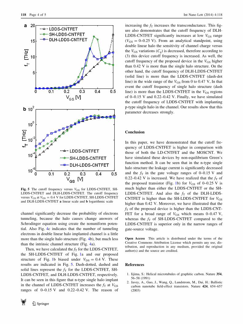
Then, we have calculated the fT for the LDDS-CNTFET,
the SH-LDDS-CNTFET of Fig. 1a and our proposed
structure of Fig. 1b biased under VDS = 0.4 V. These
results are indicated in Fig. 5. Dash-dotted, dashed and
solid lines represent the fT for the LDDS-CNTFET, SH-
LDDS-CNTFET, and DLH-LDDS-CNTFET, respectively.
It can be seen in this figure that n-type single halo implant
in the channel of LDDS-CNTFET increases the fT at VGS
ranges of 0–0.15 V and 0.22–0.42 V. The reason of
increasing the fT increases the transconductance. This fig-
ure also demonstrates that the cutoff frequency of DLH-
LDDS-CNTFET significantly increases at low VGS range
(VGS = 0–0.25 V). From an analytical standpoint, using
double linear halo the sensitivity of channel charge versus
the VGS variations (Cg) is decreased, therefore according to
(3) this device cutoff frequency is increased. As well, the
cutoff frequency of the proposed device in the VGS higher
than 0.42 V is more than the single halo structure. On the
other hand, the cutoff frequency of DLH-LDDS-CNTFET
(solid line) is more than the LDDS-CNTFET (dash-dot
line) in the wide range of the VGS from 0 to 0.47 V, In that
event the cutoff frequency of single halo structure (dash
line) is more than the LDDS-CNTFET in the VGS regions
of 0–0.15 V and 0.22–0.42 V. Finally, we have simulated
the cutoff frequency of LDDS-CNTFET with implanting
p-type single halo in the channel. Our results show that this
parameter decreases strongly.
Conclusion
In this paper, we have demonstrated that the cutoff fre-
quency of LDDS-CNTFET is higher in comparison with
those of both the LD-CNTFET and the MOSCNT. We
have simulated these devices by non-equilibrium Green’s
function method. It can be seen that in the n-type single
halo structure the leakage current is significantly decreased
and the fT in the gate voltage ranges of 0–0.15 V and
0.22–0.42 V is increased. We have realized that the fT of
the proposed transistor (Fig. 1b) for VGS of 0–0.25 V is
much higher than either the LDDS-CNTFET or the SH-
LDDS-CNTFET. And also the fT of the DLH-LDDS-
CNTFET is higher than the SH-LDDS-CNTFET for VGS
higher than 0.42 V. Moreover, we have illustrated that the
fT of the proposed device is higher than the LDDS-CNT-
FET for a broad range of VGS which means 0–0.47 V,
whereas the fT of SH-LDDS-CNTFET compared to the
LDDS-CNTFET is superior only in the narrow ranges of
gate-source voltage.
Open Access This article is distributed under the terms of the
Creative Commons Attribution License which permits any use, dis-
tribution, and reproduction in any medium, provided the original
author(s) and the source are credited.
References
1. Iijima, S.: Helical microtubules of graphitic carbon. Nature 354,
56–58 (1991)
2. Javey, A., Guo, J., Wang, Q., Lundstrom, M., Dai, H.: Ballistic
carbon nanotube field-effect transistors. Nature 424, 654–657
(2003)
Fig. 5 The cutoff frequency versus VGS for LDDS-CNTFET, SH-
LDDS-CNTFET and DLH-LDDS-CNTFET. The cutoff frequency
versus VGS at VDS = 0.4 V for LDDS-CNTFET, SH-LDDS-CNTFET
and DLH-LDDS-CNTFET a linear scale and b logarithmic scale
118 Page 4 of 5 Int Nano Lett (2014) 4:118
123

3. Javey, A., Kim, H., Brink, M., Wang, Q., Ural, A., Guo, J.,
McIntyre, P., McEuen, P., Lundstrom, M., Dai, H.: High
dielectrics for advanced carbon nanotube transistors and logic.
Nat. Mater. 1, 241–246 (2002)
4. Lin, Y.M., Appenzeller, J., Knoch, J., Avouris, P.: High perfor-
mance carbon nanotube field-effect transistor with tunable
polarities. IEEE Trans. Nanotechnol. 4, 481–489 (2005)
5. Heinze, S., Tersoff, J., Avouris, P.: Electrostatic engineering of
nanotube transistors for improved performance. Appl. Phys. Lett.
83, 5038–5040 (2003)
6. Hassaninia, I., Sheikhi, M.H., Kordrostami, Z.: Simulation of
carbon nanotube FETs with linear doping profile near the source
and drain contacts. Solid State Electron. 52, 980–985 (2008)
7. Yousefi, R., Saghafi, K., Moravvej-Farshi, M.K.: Numerical
study of lightly doped drain and source carbon nanotube field
effect transistors. IEEE Trans. Electron Devices 57, 765–771
(2010)
8. Arefinia, Z., Orouji, A.A.: Impact of single halo implantation on
the carbon nanotube field-effect transistor. A quantum simulation
study. Physica E 41, 196–201 (2008)
9. Li, J., Zhang, Q.: Simulation of ambipolar-to-unipolar conversion
of carbon nanotube based field effect transistors. Nanotechnology
16, 1415–1418 (2005)
10. Orouji, A.A., Arefinia, Z.: Detailed simulation study of a dual
material gate carbon nanotube field-effect transistor. Physica E
41, 552–557 (2009)
11. Orouji, A.A., Ahmadmiri, S.A.: Novel attributes and design
considerations of source and drain regions in carbon nanotube
transistors. Physica E 42, 1456–1462 (2010)
12. Kordrostami, Z., Sheikhi, M.H., Zarifkar, A.: Influence of chan-
nel and underlap engineering on the high-frequency and switch-
ing performance of CNTFETs. IEEE Trans. Nanotechnol. 11,
526–533 (2012)
13. Guo, J., Datta, S., Lundstrom, M., Anantram, M.P.: Toward
multi-scale simulations of carbon nanotube transistors. Int.
J. Multiscale Comput. Eng. 2, 257–276 (2004)
14. Guo, J., Datta, S., Anantram, M.P., Lundstrom, M.: Atomistic
simulation of carbon nanotube field-effect transistors using non-
equilibrium Green’s function formalism. J. Comput. Electron. 3,
373–377 (2004)
15. Datta, S.: Electronic transport in mesoscopic systems. Cambridge
University Press, Cambridge (1995)
16. Yoon, Y., Guo, J.: Analysis of strain effects in ballistic carbon
nanotube FETs. IEEE Trans. Electron Devices 54, 1280–1287
(2007)
17. Venugopal, R., Ren, Z., Datta, S., Lundstrom, M., Jovanovic, D.:
Simulating quantum transport in nanoscale transistors: real versus
mode-space approaches. J. Appl. Phys. 92, 3730–3739 (2002)
18. Alam, K., Lake, R.: Dielectric scaling of a zero-Schottky-barrier
5 nm gate carbon nanotube transistor with source/drain under-
laps. J. Appl. Phys. 100, 24317–24324 (2006)
19. Monga, U., Borliand, H., Fjeldly, T.: A compact subthreshold
current and capacitance modeling of short-channel double-gate
MOSFETs. Math. Comput. Model. 51, 901–907 (2010)
20. Yoon, Y., Yijianand, O., Jing, G.: Effect of phonon scattering on
intrinsic delay and cutoff frequency of carbon nanotube FETs.
IEEE Trans. Electron Devices 53, 2467–2470 (2006)
Int Nano Lett (2014) 4:118 Page 5 of 5 118
123