Embed Size (px)
Citation preview
Full Terms & Conditions of access and use can be found athttp://www.tandfonline.com/action/journalInformation?journalCode=tlct20
Liquid Crystals
ISSN: 0267-8292 (Print) 1366-5855 (Online) Journal homepage: http://www.tandfonline.com/loi/tlct20
Investigation on newly designed low resistivitypolyimide-type alignment layer for reducing DCimage sticking of in-plane switching liquid crystaldisplay
Tae Rim Lee, Jin Ho Kim, Seung Hee Lee, Myung Chul Jun & Hong Koo Baik
To cite this article: Tae Rim Lee, Jin Ho Kim, Seung Hee Lee, Myung Chul Jun & Hong Koo Baik(2017) Investigation on newly designed low resistivity polyimide-type alignment layer for reducingDC image sticking of in-plane switching liquid crystal display, Liquid Crystals, 44:4, 738-747, DOI:10.1080/02678292.2016.1239775
To link to this article: https://doi.org/10.1080/02678292.2016.1239775
Published online: 07 Nov 2016.
Submit your article to this journal
Article views: 162
View Crossmark data
Citing articles: 3 View citing articles
Investigation on newly designed low resistivity polyimide-type alignment layerfor reducing DC image sticking of in-plane switching liquid crystal displayTae Rim Lee a, Jin Ho Kimb, Seung Hee Leeb, Myung Chul Junc and Hong Koo Baika
aDisplay and Plasma Research Laboratory, Department of Materials Science and Engineering, Yonsei University, Seoul, South Korea;bDepartment of BIN Convergence Technology and Department of Polymer-Nano Science and Technology, Applied Materials Institute for BINConvergence, Chonbuk National University, Jeonju, South Korea; cLG Display, LG-ro, Paju-si, South Korea
ABSTRACTSoluble polyimide-type alignment layer is widely used in in-plane switching (IPS) liquid crystaldisplay (LCD) because of its excellent reliability owing to high imidisation ratio during long-termdriving, high voltage-holding ratio and low ion density. Nevertheless, it exhibits slow directcurrent (DC) discharging property due to its high resistivity, causing significant DC image-stickingproblem. In this study, we doped inorganic salt to control the resistivity of soluble polyimide-typealignment layer and found that this approach reduced DC image sticking greatly without any lossof reliability property in IPS-LCD.
ARTICLE HISTORYReceived 24 August 2016Accepted 19 September2016
KEYWORDSIn-plane switching;alignment layer; resistivity;image sticking
1. Introduction
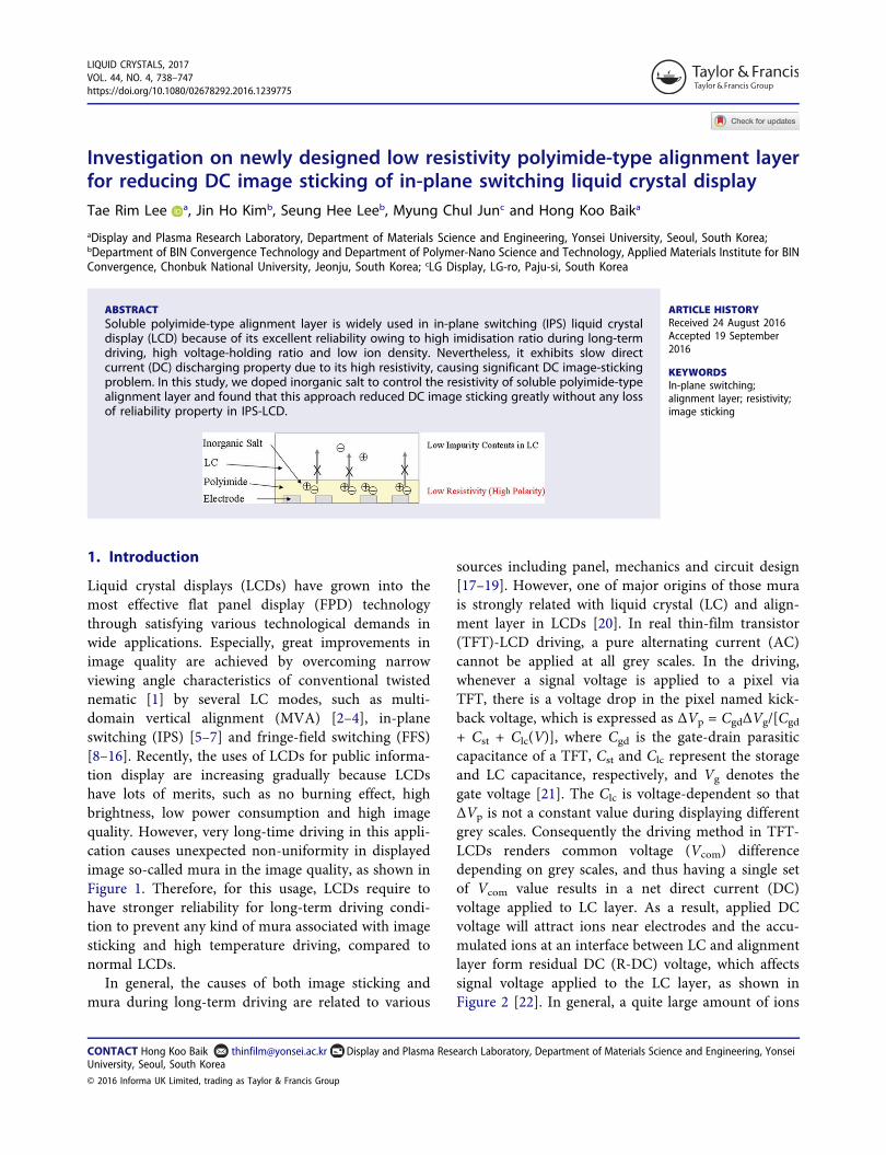
Liquid crystal displays (LCDs) have grown into themost effective flat panel display (FPD) technologythrough satisfying various technological demands inwide applications. Especially, great improvements inimage quality are achieved by overcoming narrowviewing angle characteristics of conventional twistednematic [1] by several LC modes, such as multi-domain vertical alignment (MVA) [2–4], in-planeswitching (IPS) [5–7] and fringe-field switching (FFS)[8–16]. Recently, the uses of LCDs for public informa-tion display are increasing gradually because LCDshave lots of merits, such as no burning effect, highbrightness, low power consumption and high imagequality. However, very long-time driving in this appli-cation causes unexpected non-uniformity in displayedimage so-called mura in the image quality, as shown inFigure 1. Therefore, for this usage, LCDs require tohave stronger reliability for long-term driving condi-tion to prevent any kind of mura associated with imagesticking and high temperature driving, compared tonormal LCDs.
In general, the causes of both image sticking andmura during long-term driving are related to various
sources including panel, mechanics and circuit design[17–19]. However, one of major origins of those murais strongly related with liquid crystal (LC) and align-ment layer in LCDs [20]. In real thin-film transistor(TFT)-LCD driving, a pure alternating current (AC)cannot be applied at all grey scales. In the driving,whenever a signal voltage is applied to a pixel viaTFT, there is a voltage drop in the pixel named kick-back voltage, which is expressed as ΔVp = CgdΔVg/[Cgd
+ Cst + Clc(V)], where Cgd is the gate-drain parasiticcapacitance of a TFT, Cst and Clc represent the storageand LC capacitance, respectively, and Vg denotes thegate voltage [21]. The Clc is voltage-dependent so thatΔVp is not a constant value during displaying differentgrey scales. Consequently the driving method in TFT-LCDs renders common voltage (Vcom) differencedepending on grey scales, and thus having a single setof Vcom value results in a net direct current (DC)voltage applied to LC layer. As a result, applied DCvoltage will attract ions near electrodes and the accu-mulated ions at an interface between LC and alignmentlayer form residual DC (R-DC) voltage, which affectssignal voltage applied to the LC layer, as shown inFigure 2 [22]. In general, a quite large amount of ions
CONTACT Hong Koo Baik [email protected] Display and Plasma Research Laboratory, Department of Materials Science and Engineering, YonseiUniversity, Seoul, South Korea
LIQUID CRYSTALS, 2017VOL. 44, NO. 4, 738–747https://doi.org/10.1080/02678292.2016.1239775
© 2016 Informa UK Limited, trading as Taylor & Francis Group
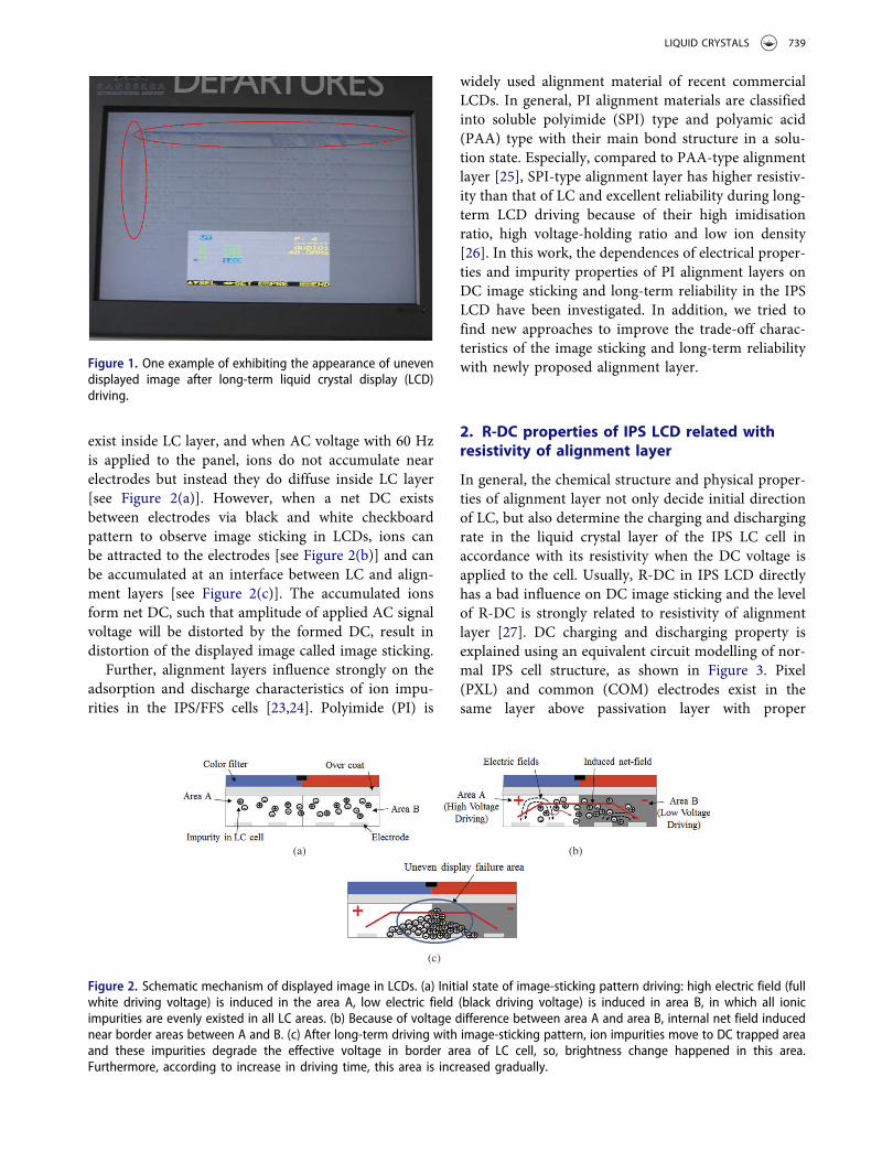
exist inside LC layer, and when AC voltage with 60 Hzis applied to the panel, ions do not accumulate nearelectrodes but instead they do diffuse inside LC layer[see Figure 2(a)]. However, when a net DC existsbetween electrodes via black and white checkboardpattern to observe image sticking in LCDs, ions canbe attracted to the electrodes [see Figure 2(b)] and canbe accumulated at an interface between LC and align-ment layers [see Figure 2(c)]. The accumulated ionsform net DC, such that amplitude of applied AC signalvoltage will be distorted by the formed DC, result indistortion of the displayed image called image sticking.
Further, alignment layers influence strongly on theadsorption and discharge characteristics of ion impu-rities in the IPS/FFS cells [23,24]. Polyimide (PI) is
widely used alignment material of recent commercialLCDs. In general, PI alignment materials are classifiedinto soluble polyimide (SPI) type and polyamic acid(PAA) type with their main bond structure in a solu-tion state. Especially, compared to PAA-type alignmentlayer [25], SPI-type alignment layer has higher resistiv-ity than that of LC and excellent reliability during long-term LCD driving because of their high imidisationratio, high voltage-holding ratio and low ion density[26]. In this work, the dependences of electrical proper-ties and impurity properties of PI alignment layers onDC image sticking and long-term reliability in the IPSLCD have been investigated. In addition, we tried tofind new approaches to improve the trade-off charac-teristics of the image sticking and long-term reliabilitywith newly proposed alignment layer.
2. R-DC properties of IPS LCD related withresistivity of alignment layer
In general, the chemical structure and physical proper-ties of alignment layer not only decide initial directionof LC, but also determine the charging and dischargingrate in the liquid crystal layer of the IPS LC cell inaccordance with its resistivity when the DC voltage isapplied to the cell. Usually, R-DC in IPS LCD directlyhas a bad influence on DC image sticking and the levelof R-DC is strongly related to resistivity of alignmentlayer [27]. DC charging and discharging property isexplained using an equivalent circuit modelling of nor-mal IPS cell structure, as shown in Figure 3. Pixel(PXL) and common (COM) electrodes exist in thesame layer above passivation layer with proper
Figure 1. One example of exhibiting the appearance of unevendisplayed image after long-term liquid crystal display (LCD)driving.
(a) (b)
(c)
Figure 2. Schematic mechanism of displayed image in LCDs. (a) Initial state of image-sticking pattern driving: high electric field (fullwhite driving voltage) is induced in the area A, low electric field (black driving voltage) is induced in area B, in which all ionicimpurities are evenly existed in all LC areas. (b) Because of voltage difference between area A and area B, internal net field inducednear border areas between A and B. (c) After long-term driving with image-sticking pattern, ion impurities move to DC trapped areaand these impurities degrade the effective voltage in border area of LC cell, so, brightness change happened in this area.Furthermore, according to increase in driving time, this area is increased gradually.
LIQUID CRYSTALS 739
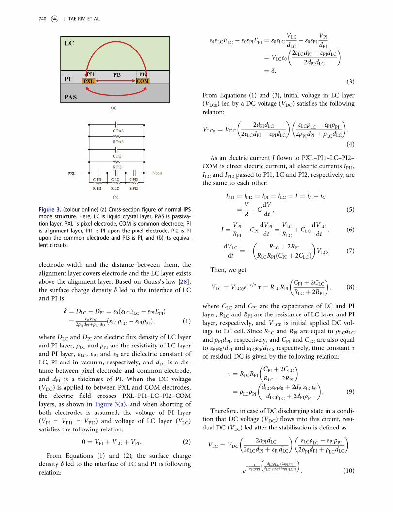
electrode width and the distance between them, thealignment layer covers electrode and the LC layer existsabove the alignment layer. Based on Gauss’s law [28],the surface charge density δ led to the interface of LCand PI is
δ ¼ DLC � DPI ¼ ε0ðεLCELC � εPIEPIÞ¼ ε0VDC
2ρPIdPIþρLCdLCðεLCρLC � εPIρPIÞ; (1)
where DLC and DPI are electric flux density of LC layerand PI layer, ρLC and ρPI are the resistivity of LC layerand PI layer, εLC, εPI and ε0 are dielectric constant ofLC, PI and in vacuum, respectively, and dLC is a dis-tance between pixel electrode and common electrode,and dPI is a thickness of PI. When the DC voltage(VDC) is applied to between PXL and COM electrodes,the electric field crosses PXL–PI1–LC–PI2–COMlayers, as shown in Figure 3(a), and when shorting ofboth electrodes is assumed, the voltage of PI layer(VPI = VPI1 = VPI2) and voltage of LC layer (VLC)satisfies the following relation:
0 ¼ VPI þ VLC þ VPI: (2)
From Equations (1) and (2), the surface chargedensity δ led to the interface of LC and PI is followingrelation:
ε0εLCELC � ε0εPIEPI ¼ ε0εLCVLC
dLC� ε0εPI
VPI
dPI
¼ VLCε02εLCdPI þ εPIdLC
2dPIdLC
� �
¼ δ:
(3)
From Equations (1) and (3), initial voltage in LC layer(VLC0) led by a DC voltage (VDC) satisfies the followingrelation:
VLC0 ¼ VDC2dPIdLC
2εLCdPI þ εPIdLC
� �εLCρLC � εPIρPI2ρPIdPI þ ρLCdLC
� �:
(4)
As an electric current I flown to PXL–PI1–LC–PI2–COM is direct electric current, all electric currents IPI1,ILC and IPI2 passed to PI1, LC and PI2, respectively, arethe same to each other:
IPI1 ¼ IPI2 ¼ IPI ¼ ILC ¼ I ¼ iR þ iC
¼ VRþ C
dVdt
; (5)
I ¼ VPI
RPIþ CPI
dVPI
dt¼ VLC
RLCþ CLC
dVLC
dt; (6)
dVLC
dt¼ � RLC þ 2RPI
RLCRPIðCPI þ 2CLCÞ� �
VLC: (7)
Then, we get
VLC ¼ VLC0e�t=τ τ ¼ RLCRPI
CPI þ 2CLC
RLC þ 2RPI
� �; (8)
where CLC and CPI are the capacitance of LC and PIlayer, RLC and RPI are the resistance of LC layer and PIlayer, respectively, and VLC0 is initial applied DC vol-tage to LC cell. Since RLC and RPI are equal to ρLCdLCand ρPIdPI, respectively, and CPI and CLC are also equalto εPIε0/dPI and εLCε0/dLC, respectively, time constant τof residual DC is given by the following relation:
τ ¼ RLCRPICPI þ 2CLC
RLC þ 2RPI
� �
¼ ρLCρPIdLCεPIε0 þ 2dPIεLCε0dLCρLC þ 2dPIρPI
� �: (9)
Therefore, in case of DC discharging state in a condi-tion that DC voltage (VDC) flows into this circuit, resi-dual DC (VLC) led after the stabilisation is defined as
VLC ¼ VDC2dPIdLC
2εLCdPI þ εPIdLC
� �εLCρLC � εPIρPI2ρPIdPI þ ρLCdLC
� �
e� t
ρLCρPI
dLCρLCþ2dPIρPIdLCεPIε0þ2dPIεLCε0
� �: (10)
(a)
(b)
Figure 3. (colour online) (a) Cross-section figure of normal IPSmode structure. Here, LC is liquid crystal layer, PAS is passiva-tion layer, PXL is pixel electrode, COM is common electrode, PIis alignment layer, PI1 is PI upon the pixel electrode, PI2 is PIupon the common electrode and PI3 is PI, and (b) its equiva-lent circuits.
740 L. TAE RIM ET AL.
On the other hand, in case of charging in a condi-tion that DC voltage (VDC) flows into this circuit,charged DC in LC layer (VLC) is defined as
VLC ¼ VDC2dPIdLC
2εLCdPI þ εPIdLC
� �εLCρLC � εPIρPI2ρPIdPI þ ρLCdLC
� �
e�ρLCρPI
tdLCεPIε0þ2dPIεLCε0dLCρLCþ2dPIρPI
� �: (11)
From Equations (10) and (11), one can understand thatR-DC (VLC) and time constant τ depend on resistivity,thickness and dielectric constant of PI layer and LClayer, in a condition that there are no new ion impu-rities generated in each layer [29].
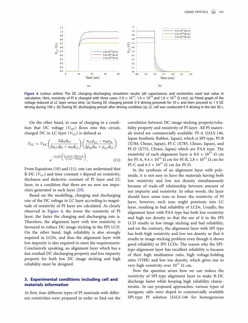
Based on the modelling, charging and dischargingrate of the DC voltage in LC layer according to magni-tude of resistivity of PI layer are calculated. As clearlyobserved in Figure 4, the lower the resistivity of PIlayer, the faster the charging and discharging rate is.Therefore, the alignment layer with low resistivity isfavoured to reduce DC image sticking in the IPS LCD.On the other hand, high reliability is also stronglyrequired in LCDs, and thus the alignment layer withlow impurity is also required to meet the requirements.Conclusively speaking, an alignment layer which has afast residual DC discharging property and low impurityproperty for both low DC image sticking and highreliability must be designed.
3. Experimental conditions including cell andmaterials information
At first, four different types of PI materials with differ-ent resistivities were prepared in order to find out the
correlation between DC image-sticking property/relia-bility property and resistivity of PI layer. All PI materi-als tested are commercially available: PI-A (JALS-146,Japan Synthetic Rubber, Japan), which is SPI type, PI-B(X784, Chisso, Japan), PI-C (X785, Chisso, Japan), andPI-D (X755, Chisso, Japan) which are PAA type. Theresistivity of each alignment layer is 8.0 × 10¹⁵ Ω cmfor PI-A, 9.4 × 10¹² Ω cm for PI-B, 2.8 × 10¹² Ω cm forPI-C and 6.3 × 10¹³ Ω cm for PI-D.
In the synthesis of an alignment layer with poly-imide, it is not easy to have the materials having bothlow resistivity and low ion density simultaneouslybecause of trade-off relationship between amount ofion impurity and resistivity. In other words, the layershould have some ions to lower the resistivity of PIlayer, however, such ions might penetrate into LClayer, resulting in bad reliability of LCDs. Usually, thealignment layer with PAA type has both low resistivityand high ion density so that the use of it in the IPSLCD results in low image sticking and bad reliability,and on the contrary, the alignment layer with SPI typehas both high resistivity and low ion density so that itresults in image-sticking problem even though it showsgood reliability in IPS LCDs. The reason why the SPI-type alignment layer has excellent reliability is becauseof their high imidisation ratio, high voltage-holdingratio (VHR) and low ion density, which gives rise tovery high resistivity over 1015 Ω cm.
Now the question arises how we can reduce theresistivity of SPI-type alignment layer to make R-DCdischarge faster while keeping high reliability charac-teristic. In our proposed approaches, various types ofinorganic salts were doped to commercially availableSPI-type PI solution (JALS-146 for homogeneous
(a) (b)
Figure 4. (colour online) The DC charging–discharging simulation results [all capacitances and resistivities used real value incalculation. Here, resistivity of PI is changed with three cases (1.0 × 10¹³, 1.0 × 10¹⁴ and 1.0 × 10¹⁵ Ω cm)]. (a) Fitted graph of thevoltage induced at LC layer versus time. (a) During DC charging period: 0 V driving proceeds for 10 s, and then proceed to 1 V DCdriving during 100 s. (b) During DC discharging period: after driving condition (a), LC cell was conducted 0 V driving in the last 30 s.
LIQUID CRYSTALS 741
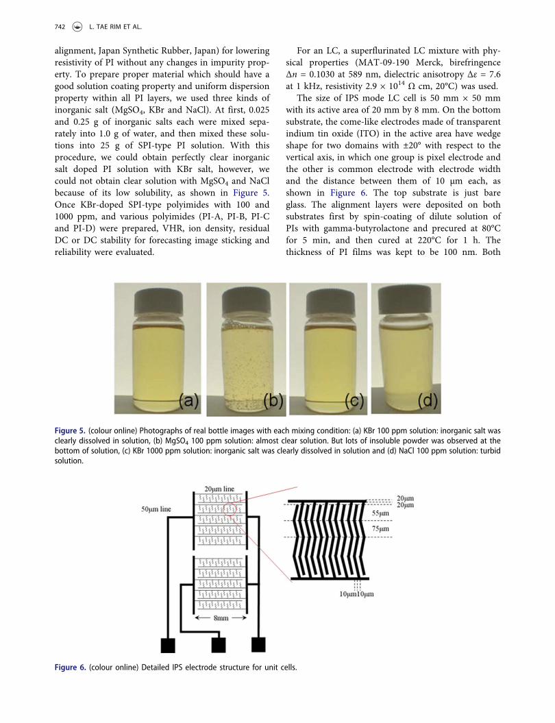
alignment, Japan Synthetic Rubber, Japan) for loweringresistivity of PI without any changes in impurity prop-erty. To prepare proper material which should have agood solution coating property and uniform dispersionproperty within all PI layers, we used three kinds ofinorganic salt (MgSO4, KBr and NaCl). At first, 0.025and 0.25 g of inorganic salts each were mixed sepa-rately into 1.0 g of water, and then mixed these solu-tions into 25 g of SPI-type PI solution. With thisprocedure, we could obtain perfectly clear inorganicsalt doped PI solution with KBr salt, however, wecould not obtain clear solution with MgSO4 and NaClbecause of its low solubility, as shown in Figure 5.Once KBr-doped SPI-type polyimides with 100 and1000 ppm, and various polyimides (PI-A, PI-B, PI-Cand PI-D) were prepared, VHR, ion density, residualDC or DC stability for forecasting image sticking andreliability were evaluated.
For an LC, a superflurinated LC mixture with phy-sical properties (MAT-09-190 Merck, birefringenceΔn = 0.1030 at 589 nm, dielectric anisotropy Δε = 7.6at 1 kHz, resistivity 2.9 × 10¹⁴ Ω cm, 20°C) was used.
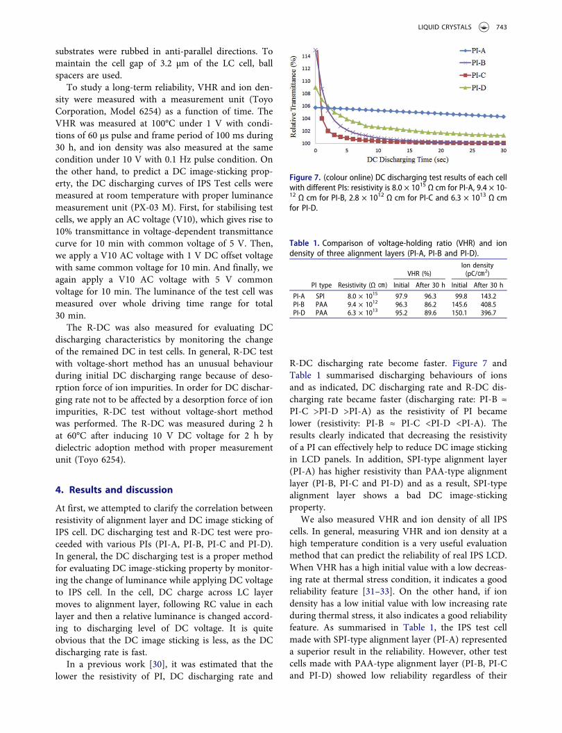
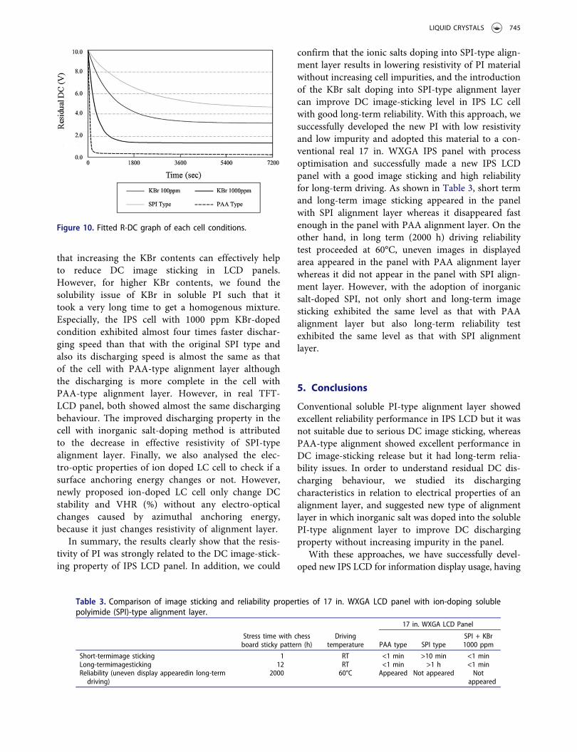
The size of IPS mode LC cell is 50 mm × 50 mmwith its active area of 20 mm by 8 mm. On the bottomsubstrate, the come-like electrodes made of transparentindium tin oxide (ITO) in the active area have wedgeshape for two domains with ±20° with respect to thevertical axis, in which one group is pixel electrode andthe other is common electrode with electrode widthand the distance between them of 10 µm each, asshown in Figure 6. The top substrate is just bareglass. The alignment layers were deposited on bothsubstrates first by spin-coating of dilute solution ofPIs with gamma-butyrolactone and precured at 80°Cfor 5 min, and then cured at 220°C for 1 h. Thethickness of PI films was kept to be 100 nm. Both
Figure 5. (colour online) Photographs of real bottle images with each mixing condition: (a) KBr 100 ppm solution: inorganic salt wasclearly dissolved in solution, (b) MgSO4 100 ppm solution: almost clear solution. But lots of insoluble powder was observed at thebottom of solution, (c) KBr 1000 ppm solution: inorganic salt was clearly dissolved in solution and (d) NaCl 100 ppm solution: turbidsolution.
Figure 6. (colour online) Detailed IPS electrode structure for unit cells.
742 L. TAE RIM ET AL.
substrates were rubbed in anti-parallel directions. Tomaintain the cell gap of 3.2 µm of the LC cell, ballspacers are used.
To study a long-term reliability, VHR and ion den-sity were measured with a measurement unit (ToyoCorporation, Model 6254) as a function of time. TheVHR was measured at 100°C under 1 V with condi-tions of 60 µs pulse and frame period of 100 ms during30 h, and ion density was also measured at the samecondition under 10 V with 0.1 Hz pulse condition. Onthe other hand, to predict a DC image-sticking prop-erty, the DC discharging curves of IPS Test cells weremeasured at room temperature with proper luminancemeasurement unit (PX-03 M). First, for stabilising testcells, we apply an AC voltage (V10), which gives rise to10% transmittance in voltage-dependent transmittancecurve for 10 min with common voltage of 5 V. Then,we apply a V10 AC voltage with 1 V DC offset voltagewith same common voltage for 10 min. And finally, weagain apply a V10 AC voltage with 5 V commonvoltage for 10 min. The luminance of the test cell wasmeasured over whole driving time range for total30 min.
The R-DC was also measured for evaluating DCdischarging characteristics by monitoring the changeof the remained DC in test cells. In general, R-DC testwith voltage-short method has an unusual behaviourduring initial DC discharging range because of deso-rption force of ion impurities. In order for DC dischar-ging rate not to be affected by a desorption force of ionimpurities, R-DC test without voltage-short methodwas performed. The R-DC was measured during 2 hat 60°C after inducing 10 V DC voltage for 2 h bydielectric adoption method with proper measurementunit (Toyo 6254).
4. Results and discussion
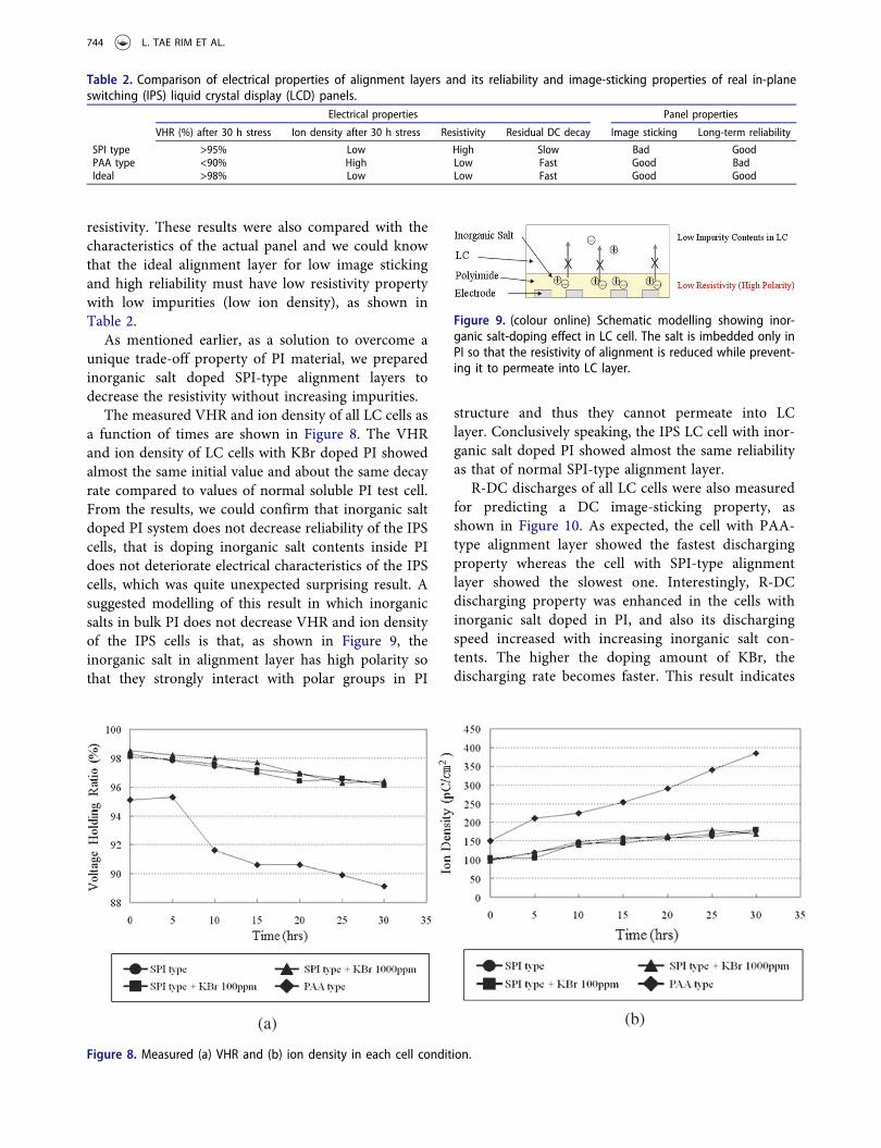
At first, we attempted to clarify the correlation betweenresistivity of alignment layer and DC image sticking ofIPS cell. DC discharging test and R-DC test were pro-ceeded with various PIs (PI-A, PI-B, PI-C and PI-D).In general, the DC discharging test is a proper methodfor evaluating DC image-sticking property by monitor-ing the change of luminance while applying DC voltageto IPS cell. In the cell, DC charge across LC layermoves to alignment layer, following RC value in eachlayer and then a relative luminance is changed accord-ing to discharging level of DC voltage. It is quiteobvious that the DC image sticking is less, as the DCdischarging rate is fast.
In a previous work [30], it was estimated that thelower the resistivity of PI, DC discharging rate and
R-DC discharging rate become faster. Figure 7 andTable 1 summarised discharging behaviours of ionsand as indicated, DC discharging rate and R-DC dis-charging rate became faster (discharging rate: PI-B ≈PI-C >PI-D >PI-A) as the resistivity of PI becamelower (resistivity: PI-B ≈ PI-C <PI-D <PI-A). Theresults clearly indicated that decreasing the resistivityof a PI can effectively help to reduce DC image stickingin LCD panels. In addition, SPI-type alignment layer(PI-A) has higher resistivity than PAA-type alignmentlayer (PI-B, PI-C and PI-D) and as a result, SPI-typealignment layer shows a bad DC image-stickingproperty.
We also measured VHR and ion density of all IPScells. In general, measuring VHR and ion density at ahigh temperature condition is a very useful evaluationmethod that can predict the reliability of real IPS LCD.When VHR has a high initial value with a low decreas-ing rate at thermal stress condition, it indicates a goodreliability feature [31–33]. On the other hand, if iondensity has a low initial value with low increasing rateduring thermal stress, it also indicates a good reliabilityfeature. As summarised in Table 1, the IPS test cellmade with SPI-type alignment layer (PI-A) representeda superior result in the reliability. However, other testcells made with PAA-type alignment layer (PI-B, PI-Cand PI-D) showed low reliability regardless of their
Figure 7. (colour online) DC discharging test results of each cellwith different PIs: resistivity is 8.0 × 10¹⁵ Ω cm for PI-A, 9.4 × 10⁻¹² Ω cm for PI-B, 2.8 × 10¹² Ω cm for PI-C and 6.3 × 10¹³ Ω cmfor PI-D.
Table 1. Comparison of voltage-holding ratio (VHR) and iondensity of three alignment layers (PI-A, PI-B and PI-D).
PI type Resistivity (Ω ㎝)
VHR (%)Ion density(pC/㎝2)
Initial After 30 h Initial After 30 h
PI-A SPI 8.0 × 10¹⁵ 97.9 96.3 99.8 143.2PI-B PAA 9.4 × 10¹² 96.3 86.2 145.6 408.5PI-D PAA 6.3 × 10¹³ 95.2 89.6 150.1 396.7
LIQUID CRYSTALS 743
resistivity. These results were also compared with thecharacteristics of the actual panel and we could knowthat the ideal alignment layer for low image stickingand high reliability must have low resistivity propertywith low impurities (low ion density), as shown inTable 2.
As mentioned earlier, as a solution to overcome aunique trade-off property of PI material, we preparedinorganic salt doped SPI-type alignment layers todecrease the resistivity without increasing impurities.
The measured VHR and ion density of all LC cells asa function of times are shown in Figure 8. The VHRand ion density of LC cells with KBr doped PI showedalmost the same initial value and about the same decayrate compared to values of normal soluble PI test cell.From the results, we could confirm that inorganic saltdoped PI system does not decrease reliability of the IPScells, that is doping inorganic salt contents inside PIdoes not deteriorate electrical characteristics of the IPScells, which was quite unexpected surprising result. Asuggested modelling of this result in which inorganicsalts in bulk PI does not decrease VHR and ion densityof the IPS cells is that, as shown in Figure 9, theinorganic salt in alignment layer has high polarity sothat they strongly interact with polar groups in PI
structure and thus they cannot permeate into LClayer. Conclusively speaking, the IPS LC cell with inor-ganic salt doped PI showed almost the same reliabilityas that of normal SPI-type alignment layer.
R-DC discharges of all LC cells were also measuredfor predicting a DC image-sticking property, asshown in Figure 10. As expected, the cell with PAA-type alignment layer showed the fastest dischargingproperty whereas the cell with SPI-type alignmentlayer showed the slowest one. Interestingly, R-DCdischarging property was enhanced in the cells withinorganic salt doped in PI, and also its dischargingspeed increased with increasing inorganic salt con-tents. The higher the doping amount of KBr, thedischarging rate becomes faster. This result indicates
Table 2. Comparison of electrical properties of alignment layers and its reliability and image-sticking properties of real in-planeswitching (IPS) liquid crystal display (LCD) panels.
Electrical properties Panel properties
VHR (%) after 30 h stress Ion density after 30 h stress Resistivity Residual DC decay Image sticking Long-term reliability
SPI type >95% Low High Slow Bad GoodPAA type <90% High Low Fast Good BadIdeal >98% Low Low Fast Good Good
(a) (b)
Figure 8. Measured (a) VHR and (b) ion density in each cell condition.
Figure 9. (colour online) Schematic modelling showing inor-ganic salt-doping effect in LC cell. The salt is imbedded only inPI so that the resistivity of alignment is reduced while prevent-ing it to permeate into LC layer.
744 L. TAE RIM ET AL.
that increasing the KBr contents can effectively helpto reduce DC image sticking in LCD panels.However, for higher KBr contents, we found thesolubility issue of KBr in soluble PI such that ittook a very long time to get a homogenous mixture.Especially, the IPS cell with 1000 ppm KBr-dopedcondition exhibited almost four times faster dischar-ging speed than that with the original SPI type andalso its discharging speed is almost the same as thatof the cell with PAA-type alignment layer althoughthe discharging is more complete in the cell withPAA-type alignment layer. However, in real TFT-LCD panel, both showed almost the same dischargingbehaviour. The improved discharging property in thecell with inorganic salt-doping method is attributedto the decrease in effective resistivity of SPI-typealignment layer. Finally, we also analysed the elec-tro-optic properties of ion doped LC cell to check if asurface anchoring energy changes or not. However,newly proposed ion-doped LC cell only change DCstability and VHR (%) without any electro-opticalchanges caused by azimuthal anchoring energy,because it just changes resistivity of alignment layer.
In summary, the results clearly show that the resis-tivity of PI was strongly related to the DC image-stick-ing property of IPS LCD panel. In addition, we could
confirm that the ionic salts doping into SPI-type align-ment layer results in lowering resistivity of PI materialwithout increasing cell impurities, and the introductionof the KBr salt doping into SPI-type alignment layercan improve DC image-sticking level in IPS LC cellwith good long-term reliability. With this approach, wesuccessfully developed the new PI with low resistivityand low impurity and adopted this material to a con-ventional real 17 in. WXGA IPS panel with processoptimisation and successfully made a new IPS LCDpanel with a good image sticking and high reliabilityfor long-term driving. As shown in Table 3, short termand long-term image sticking appeared in the panelwith SPI alignment layer whereas it disappeared fastenough in the panel with PAA alignment layer. On theother hand, in long term (2000 h) driving reliabilitytest proceeded at 60°C, uneven images in displayedarea appeared in the panel with PAA alignment layerwhereas it did not appear in the panel with SPI align-ment layer. However, with the adoption of inorganicsalt-doped SPI, not only short and long-term imagesticking exhibited the same level as that with PAAalignment layer but also long-term reliability testexhibited the same level as that with SPI alignmentlayer.
5. Conclusions
Conventional soluble PI-type alignment layer showedexcellent reliability performance in IPS LCD but it wasnot suitable due to serious DC image sticking, whereasPAA-type alignment showed excellent performance inDC image-sticking release but it had long-term relia-bility issues. In order to understand residual DC dis-charging behaviour, we studied its dischargingcharacteristics in relation to electrical properties of analignment layer, and suggested new type of alignmentlayer in which inorganic salt was doped into the solublePI-type alignment layer to improve DC dischargingproperty without increasing impurity in the panel.
With these approaches, we have successfully devel-oped new IPS LCD for information display usage, having
Figure 10. Fitted R-DC graph of each cell conditions.
Table 3. Comparison of image sticking and reliability properties of 17 in. WXGA LCD panel with ion-doping solublepolyimide (SPI)-type alignment layer.
Stress time with chessboard sticky pattern (h)
Drivingtemperature
17 in. WXGA LCD Panel
PAA type SPI typeSPI + KBr1000 ppm
Short-termimage sticking 1 RT <1 min >10 min <1 minLong-termimagesticking 12 RT <1 min >1 h <1 minReliability (uneven display appearedin long-termdriving)
2000 60°C Appeared Not appeared Notappeared
LIQUID CRYSTALS 745
both long-term reliability and low image-sticking level.Conclusively speaking, we could confirm that inorganicsalt-doping method can reduce bulk resistivity of bulk PIlayer without increasing ionic impurities in LC layer. Nodoubt, this new technology will simply provide the betterperformance for long-term driving usage of IPS LCD.
Acknowledgements
We deeply appreciate the LCD Materials Laboratory of JSRCorporation for their kind supports in the researches.
Disclosure statement
No potential conflict of interest was reported by the authors.
ORCID
Tae Rim Lee http://orcid.org/0000-0003-1860-8236
References
[1] Lee SH, Bhattacharyya SS, Jin HS, et al. Devices andmaterials for high performance mobile liquid crystaldisplays. J Mater Chem. 2012;22:11893–11903.DOI:10.1039/c2jm30635b.
[2] Koma N, Yaba Y, Matsuoka K. No-rub multi-domainTFT-LCD using surrounding-electrode method. SID IntSymp Dig Tech Pap. 1995;26:869–872.
[3] Lee SH, Kim SM, Wu ST. Emerging vertical-alignmentliquid-crystal technology associated with surface modi-fication using UV-curable monomer. J Soc Inf Disp.2009;17:551–559. DOI:10.1889/JSID17.7.551.
[4] Seiberle H, Schadt M. Photo-alignment and patterning ofplanar and homeotropic liquid crystal display configura-tions. In: Proceeding of the 18th International DisplayResearch Conference and Asia Display; Sep 28–Oct 1;Seoul: Society for Information Display; 1998. p. 193–198.
[5] Kiefer R, Weber B, Windscheid F, et al. In-plane switch-ing of nematic liquid crystals. In: Proceeding of the 12thInternational Display Research Conference and JapanDisplay; Oct 12–14; Hiroshima: Society forInformation Display; 1992. p. 547–550.
[6] Oh-e M, Kondo K. Electro-optical characteristics andswitching behavior of the in-plane switching mode. ApplPhys Lett. 1995;67:3895–3897. DOI:10.1063/1.115309.
[7] Kondo K, Matsuyama S, Konishi N, et al. Invited paper:materials and components optimization for IPS TFT-LCDs. SID Int Symp Dig Tech Pap. 1998;29:389–392.DOI:10.1889/1.1833774.
[8] Lee SH, Lee SL, Kim HY. Electro-optic characteristicsand switching principle of a nematic liquid crystal cellcontrolled by fringe-field switching. Appl Phys Lett.1998;73:2881–2883. DOI:10.1063/1.122617.
[9] Lee SH, Lee SL, Kim HY. High-transmittance, wide-viewing-angle nematic liquid crystal display controlledby fringe-field switching. In: Proceeding of the18thInternational Display Research Conference and Asia
Display; Sep 28–Oct 1; Seoul: Society for InformationDisplay; 1998. p. 371–374.
[10] Lee SH, Lee SL, Kim HY, et al. 16.4L: Late-News Paper:a novel wide-viewing-angle technology: ultratransview™. SID Int Symp Dig Tech Pap. 1999;30:202–205.DOI:10.1889/1.1833995.
[11] Lee SH, Lee SM, Kim HY, et al. 29.2: 18.1ʺ Ultra-FFSTFT-LCD with super image quality and fast responsetime. SID Int Symp Dig Tech Pap. 2001;32:484–487.DOI:10.1889/1.1831901.
[12] Lee KH, Kim HY, Song SH, et al. 34.1: super-highperformance of 12.1-in. XGA tablet PC and 15-in.UXGA panel with advanced pixel concept. SID IntSymp Dig Tech Pap. 2004;35:1102–1105. DOI:10.1889/1.1821320.
[13] Yu IH, Song IS, Lee JY, et al. Intensifying the density ofa horizontal electric field to improve light efficiency in afringe-field switching liquid crystal display. J Phys D:Appl Phys. 2006;39(11):2367–2372. DOI:10.1088/0022-3727/39/11/009.
[14] Park JW, Ahn YJ, Jung JH, et al. Liquid crystal displayusing combined fringe and in-plane electric fields. ApplPhys Lett. 2008;93(8):081103. DOI:10.1063/1.2973152.
[15] Ge Z, Wu ST, Kim SS, et al. Thin cell fringe-field-switching liquid crystal display with a chiral dopant.Appl Phys Lett. 2008;92(18):181109. DOI:10.1063/1.2918838.
[16] Yun HJ, Jo MH, Jang IW, et al. Achieving high lightefficiency and fast response time in fringe field switch-ing mode using a liquid crystal with negative dielectricanisotropy. Liq Cryst. 2012;39(9):1–8. DOI:10.1080/02678292.2012.700078.
[17] Xu D, Peng F, Chen H, et al. Image sticking in liquidcrystal displays with lateral electric fields. J Appl Phys.2014;19:193102. DOI:10.1063/1.4902083.
[18] Mizusaki M, Nakanish Y, Enomoto S, et al. Evaluationof image sticking property on liquid crystal displayswith polymer layers produced from phenanthrene-car-rying monomers. Liq Cryst. 2016;9:1208–1214.DOI:10.1080/02678292.2016.1163742.
[19] Mizusaki M, Nakanish Y. Improvement of image stick-ing on liquid crystal displays with polymer layers pro-duced from mixed monomers. Liq Cryst. 2016;43(6):704–710. DOI:10.1080/02678292.2016.1140240.
[20] Park HJ, Lai L, Lin SH, et al. P-1: Analysis of IPS mura,image-sticking and flicker caused by internal DC effects.Journal of the SID. 2003;34:204–207. DOI:10.1889/1.1832238.
[21] Tsukada T. TFT/LCD Liquid-crystal displays addressedby thin-film transistor. London: CRC Press; 1996.
[22] Sawada A, Tarumi K, Naemura S. Effects of electricdouble layer and space charge polarization by pluralkinds of ions on complex dielectric constant of liquidcrystal materials. Jpn J Appl Phys. 1999;38:1418–1422.
[23] Lu L, Bhowmik A, Bos P. The effect of dielectric con-stant on ion adsorption in liquid crystal devices. LiqCryst. 2013;40:7–13.
[24] Ley E, Meyere A, Maximus B, et al. Ionic effects inLCD’s. Liq Solid State Cryst. 1992;1845:391–399.
[25] Tsutsui K, Sakai T, Goto K, et al. An image sticking-freenovel alignment material for IPS-LCD. SID Int SympDig Tech Pap. 2003;34:1166–1169.
746 L. TAE RIM ET AL.
[26] Michinori N, Takayoshi S, Yusuke T, et al. Properties ofvoltage holding ratios liquid crystal cells using organic-solvent-soluble polyimide alignment films. Jpn J ApplPhys. 1994;33:L1113–L1116.
[27] Kim YY, Kin JH, Hahn EJ, et al. Residual DC character-istics in the in-plane switching liquid crystal display bythe capacitance-voltage hysteresis method on a polymersurface. Liq Cryst. 2002;29(8):1051–1054.
[28] David JG. Introduction to electrodynamics. UpperSaddle River (NJ): Prentice-Hall; 1999.
[29] Murakami S, Iga H, Naito H. Dielectric properties ofnematic liquid crystals in the ultralow frequency regime.J Appl Phys. 1996;80:6396–6399.
[30] Kim DH, Kin JH, Kwon YR, et al. Investigation onion movement in the fringe-field switching mode
depending on resistivity of alignment layer anddielectric anisotropic sign of liquid crystal. Liq Cryst.2015;42(4):1–6.
[31] Lym YN, Lee TR, Park BG, et al. DC Influencebetween pixel electrode and alignment layer in in-plane switching mode LCD. IMID DIGEST. 2009;P1–47:677–680.
[32] Masahito O, Katsumi K. Advantageous voltae-holdingratio characteristics induced by in-plane electric fields,and the optimization concept of liquid crystals for anin-plane-switching electro-optical effect. Liq Cryst.1988;25(6):699–709.
[33] Masahito O, Yoshiyuki U. Unusual voltage-holdingratio characteristics using in-plane switching of nematicliquid cyrstals. Jpn J Appl Phys. 1997;36:1025.
LIQUID CRYSTALS 747