Embed Size (px)
Citation preview

1
1
Irreversible metal-insulator transition in thin film VO2 induced by soft X-ray irradiation
V. R. Singh1, 2*, V. Jovic3, I. Valmianski4, J. G. Ramirez4,5, B. Lamoureux1, Ivan K. Schuller4 and K. E. Smith1, 3
1Department of Physics, Boston University, Boston, MA 02215, USA 2Department of Physics, Central University of Kashmir, Srinagar, J & K 190004, India
3School of Chemical Sciences and The MacDiarmid Institute for Advanced Materials and Nanotechnology, the University of Auckland, Auckland, 92019 New Zealand
4Department of Physics and Center for Advanced Nanoscience, University of California San Diego, La Jolla, California 92093, USA
5Department of Physics, Universidad de los Andes, Bogotá 111711, Colombia
Abstract: In this study, we show the ability of soft x-ray irradiation to induce a room
temperature metal-insulator transitions (MIT) in VO2 thin films grown on R-plane sapphire. The
ability of soft x-rays to induce the MIT in VO2 thin films is confirmed by photoemission
spectroscopy and soft x-ray spectroscopy measurements. When irradiation was discontinued, the
systems do not return to the insulating phase. Analysis of valence band photoemission spectra
revealed that the density of states (DOS) of the V 3d band increased with irradiation time, while
the DOS of the O 2p band decreased. We use these results to propose a model in which the MIT
is driven by oxygen desorption from thin films during irradiation.
Introduction: As a strongly correlated transition metal oxide, VO2 is an interesting and
valuable material both for expanding our understanding of fundamental physics and for potential
applications due to its particular metal–insulator transition (MIT). At 340K, the resistance of
bulk VO2 exhibits a large jump (up to 5 orders of magnitude), accompanied by first order crystal
phase transition from a room temperature monoclinic phase to a high temperature tetragonal
phase [1-2]. The origin of the MIT has been widely discussed since electron–phonon interaction
(Peierls type) or electron–electron interaction (Mott–Hubbard type) could play a key role to
induce the occurrence of the MIT [3-7]. Furthermore, these characteristics of VO2 material make
it suitable for applications in many fields such as sensors, memory devices, photoconductive
infrared detectors, smart windows, and optical switching devices such as terahertz modulators [8-
15].
VO2 does have a relatively high critical transition temperature (Tc) that limits its practical
application. Thus modulating the phase transition behavior and decreasing Tc have become
important topics that have recently been explored. Various models and approaches to decrease
2
2
the Tc value, such as interfacial strain [16-22], hydrogenation [23-24], oxygen vacancies [25-27]
and element doping [28-30] have been employed. Among these, it has been shown that
interfacial strain has been the most effective way to reduce the Tc to room temperature or lower.
Studies have also been conducted on the photo-induced properties of VO2, including UV
light irradiation (365 nm) [31], hard X-ray irradiation (10 keV) of W doped VO2 thin films
resulting in a persistent MIT at low temperatures [32]. Similar persistent effects have also been
observed in VO2 films with 10 keV X-ray irradiation [33]. Thus, it is clear that the MIT of VO2
thin films can be tuned by light with photon energies between the meV orders to 10 keV.
In this work, we study the effect of soft x-ray irradiation on the MIT of VO2 thin films
using synchrotron radiation-based photoemission spectroscopy (PES) and x-ray absorption
spectroscopy (XAS). Our measurements suggest that continuous soft x-ray irradiation renders
the insulating state metallic in the film. We focus on the effects of soft x-ray irradiation on the
valence band structure and map the V 3d and O 2p partial density of states (pDOS) using PES
and XAS. The formation of oxygen vacancies in areas exposed to soft x-ray irradiation is
proposed as the underlying mechanism. Following the concept of chemistry driven MIT, we
show that soft x-ray induced oxygen vacancies can be a key button to tune the MIT behavior for
optoelectronic applications.
Methods: Thin films of VO2 (~100nm) were grown on (0 1 2)-oriented substrates of R-
plane sapphire, as described previously [34]. The films are hereafter referred to as VO2 (100). X-
ray diffraction (XRD) using monochromatic Cu Kα radiation and atomic force microscopy
(AFM) were used to characterize the structural properties of VO2 thin films deposited on R-plane
sapphire by magnetron sputtering [34]. XRD analysis indicated that the film orientations were
along the (100) plane, with a thickness of ~100nm [34]. AFM verified that the films surface
morphology was flat and smooth [1]. The MIT temperature was found to be 348K (for VO2
(100)) using a four-point probe method performed using a physical property measurement
system (Quantum Design PPMS) [34].
X-ray absorption and photoemission spectroscopy were performed at beamlines 8.0.1 and
10.0.1, respectively, of the Advanced Light Source, Lawrence Berkeley National Laboratory. To
study the effects of soft X-ray irradiation on the MIT via XAS, the samples were exposed to
550 eV X-rays carrying a flux density of ~1.5 × 10¹⁶ photons s-1cm-2. XAS spectra were
measured in the surface sensitive (~5 nm) total electron yield (TEY) mode. Since X-rays interact
3
3
with the materials surface even if this interaction may be very weak. By controlling the flux
density one can use the photon-beam to create oxygen vacancies in a thin layer below the surface
in a controlled but continuous way. This has been exemplified in a number of publications
concerning the use of soft X-ray spectroscopy in the study of metal-oxide systems [34A]. The x-
ray beam was perpendicular to the surface of the sample. XAS spectra were calibrated using the
O K-edge of a TiO2 rutile reference sample. The spectral resolution was 0.3 eV. Photoemission
spectra were collected at room temperature using 55 eV incident photons and calibrated against
the 4f peaks of metallic gold reference foil in electrical contact with the sample. Effects of soft
X-ray irradiation on the MIT were investigated by exposing the samples to 250 eV photons and a
flux density of 3 × 10¹⁵ photons s-1cm-2.
Results and discussions: Figure 1 shows valence band spectra of VO2 (100) thin film following
0 and 60 min exposure times to 250 eV photons. The spectra are similar to our earlier PES
measurements of vanadium oxide films and show the characteristic V 3d band stretching from 0
to 2.5 eV above the Fermi level (EF) and a broad O 2p band from 2.5 to 10 eV [35-36]. Prior to
irradiation, the V 3d states are relatively narrow and of lower intensity. The intensity of the V 3d
states at EF increases and the leading edge has a ~0.3eV shift toward lower binding energy after
60 min of irradiation. This suggests that a percentage of the material has transitioned from the
insulating to the metallic phase. Furthermore, the valence band spectrum collected 60 min after
irradiation was discontinued (red line) indicating that the soft X-ray irradiation damage was
persistent and that the material undergoes a MIT.
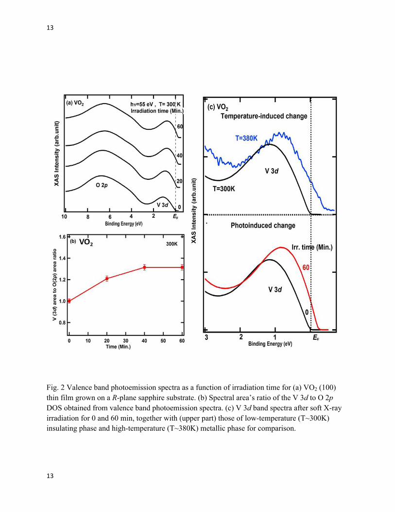
To further investigate the influence of soft x-rays on the MIT, the valence band spectrum of
the film was measured at 20-minute-irradiation intervals at particular spot on same sample as
shown in Fig 2(a). We observed a finite intensity at EF after 20 min and increasing until 40 min
soft x-ray irradiation intervals of same sample and same particular spot. Thus, this result suggests
that a minimum irradiation time is necessary for MIT induced by soft x-ray exposure. Since the
spectral area correlates with the density of state (DOS) [37], we have calculated the change in
spectral area of the V 3d and O 2p bands with irradiation time. We also calculated the ratio of the
spectral area of V 3d to O 2p DOS obtained from valence band PES as a function of irradiation
time. This is shown in Fig. 2(b). If we consider the ratio between the area of O 2p and V 3d
states, it becomes apparent that irradiation is causing oxygen to desorb. It is observed that the
DOS for V 3d increases due to a decrease in oxidation state of V, while the DOS for O 2p
4
4
decreases as a result of being freed from the lattice. At an exposure time of 40 minutes, oxygen
desorption has reached its limit, as signified by the plateau in the peak area of Fig 2(b). This
steady state indicates a saturation of the V 3d DOS.
The metallic phase induced by soft x-ray irradiation can be understood by examining
the V 3d states. The lower part of Fig. 2(c) shows the valence band spectra near EF at irradiation
times 0 and 60 min. For comparison VO2 thin films spectra near EF are also shown in Fig 2(c) for
both low-temperature (T~300K) insulating phase and high-temperature (T~380K) metallic
phase. Our results indicate that as irradiation time is increasing, the shape of V 3d band changes
and the spectral weight is transferred from a binding energy of about 0.3eV to a region near the
Fermi level. This change in the shape of the spectra that coincides with the MIT cannot be
explained by a rigid band model, where only the position of the Fermi level shifts without any
change in shape of DOS when the number of electrons is varied. The observed temperature-
induced spectra (upper panel in Fig. 2c) appear to be similar to that of photo-induced spectra at
low-temperature. These results indicate that irradiation can induce a metallic state that is
equivalent to a temperature induced metallic state.
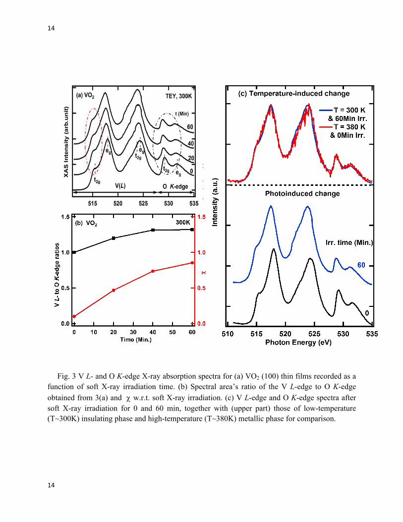
To confirm the possibility of oxygen desorption during soft x-ray irradiation suggested by
our PES measurements, we carried out another independent experimental study. Here, we used
XAS in the surface-sensitive TEY mode to measure changes in the V L3,2- and O K-edge of the
VO2 thin films. The lower spectrum of Fig. 3(a) shows V L3,2 and O K-edge XAS spectra for
VO2(100) thin film recorded at room-temperature prior to irradiation [38]. The absence of any
shift in the bulk sensitive mode V L3,2 spectra (not shown here) indicates that the vanadium ions
in VO2 thin films are in the expected V4+ oxidation state, with no indications of mixed valence
states in either the surface-sensitive and bulk-sensitive modes. These spectra are also consistent
with shape and peak positions from previous studies [38] which also confirm the purity of the
VO2 thin film.
To further probe the effects of soft x-ray irradiation with higher flux density on the
electronic structure of VO2 thin film, we performed V L3,2- and O K-edge XAS as a function of
x-ray irradiation time in both; surface and bulk sensitive TEY and TFY mode, respectively. For
XAS measurement we used same sample at different spot than PES measurements. Figure 3(a)
shows V L-edge and O K-edge absorption spectra for VO2 thin film following 0 and 60 minutes
exposure times to 550 eV x-rays carrying a flux density of 1.5 × 10¹⁶ photons s-1cm-2. Shifts in
5
5
the spectral weight of the peaks away from the reported ratios, deviations of the intensity ratio
between the spin-orbit-split 2p3/2 (L3) and 2p1/2 (L2) doublet from a 2:1 ratio, and a decrease in
the apparent spin-orbit coupling in XAS at ~6.4 eV (as compared to an XPS value of 7.3 eV) are
common features that display no dependence on irradiation time [39]. It is worth noting that
there are two subtle features within the XAS spectra which show variation before and after the
samples are irradiated. First, the V L3-edge, circled in red, shows an increase in weight after
irradiation, which is consistent with the band gap closing upon exposure. However, the O K-edge
region exhibits only slight changes before and after irradiation. Thus, the lower energy features
are associated with the V-V bonds along the c-axis. Second, there is an evident change in the t2g
and eg peak intensity ratio at the O K-edge following irradiation, indicated by the black circle,
which is a likely result of structural distortions of the VO6 octahedra [40-41]. This suggests that
the V 3d states feel the effect of the crystal field more strongly, which increases the crystal field
splitting energy, before irradiation. In other words, samples before irradiation should have a
larger separation between t2g and eg states [40-41].
Oxygen desorption can also be probed by considering the peak area (V L-edge and O K-
edge) of the x-ray absorption signal, as described in relation to PES (Fig. 2 (b)). From the plots at
the V L-edge in Fig. 3 (a), it is clear that the irradiated spectra show a shift at the low energy
edge and variations in the electronic features, resulting from changes in hybridization between
V-O states. A clearer picture of this is portrayed by Fig. 3(b), which shows V L- and O K-edge
spectral peak ratios for VO2 as a function of soft x-ray irradiation time. From this plot, it
becomes apparent that the intensities at the V L-edge are also increasing, while O K-edge
intensities are decreasing (up to an irradiation time of 40 minutes) for VO2 samples. We have
also calculated c which is equal to sqrt (integral ((x1(E)-x2(E))2 dE) / (Delta E)) where x1 and x2
are intensities obtained from fig. 3(a) and the samples which were annealed in oxygen
atmosphere for 1hr as shown in Fig.4 (black line). Thus, both XAS and PES support the
desorption of oxygen atoms from the lattice, with a critical point for the saturation of the DOS in
both the vanadium and oxygen sites at approximately 40 min of irradiation time. For comparison
spectra of VO2 thin film at V L3,2- and O K-edge are also shown in Fig 3(c) for both low-
temperature insulating phase and high-temperature metallic phase. With increasing irradiation
time, the shape of the V L3, 2- and O K-edge changes; the spectral weight is transferred towards
lower photon energy. The observed spectral change seems to be similar to that of the
6
6
temperature-induced spectra (upper panel in Fig. 3c). This implies that the high-temperature
metallic state is nearly equivalent to soft x-ray irradiation induced metallic state, obtained at low
temperature, and that they are both in the rutile-type tetragonal phase. The role of oxygen
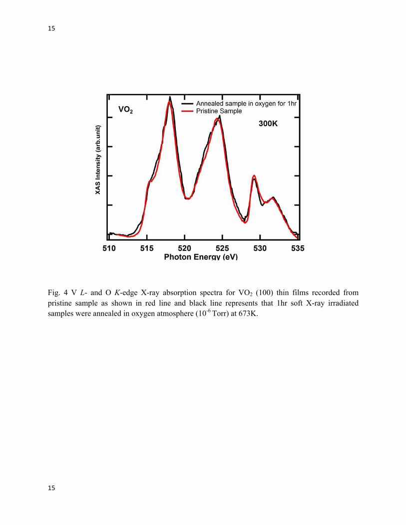
desorption from the thin films was further verified by annealing soft x-ray exposed VO2 films in
oxygen atmospheres (10-6 Torr) at 673 K for 60 min. In comparison to the pristine sample, XAS
spectrum is the slightly different, which could be due to the sample’s damage due to X-ray
irradiation but it is nearly identical in shape.
Based on our PES and XAS observations, a tentative model has been developed to
explain soft x-ray induced phase transitions in VO2 thin film. In this model, the MIT is driven by
desorption of oxygen from the lattice on account of soft x-ray exposure. Oxygen desorption
lowers the oxidation state of vanadium in VO2 thin films, thus maintaining the charge balance
and driving the MIT to completion [42-43]. Agreement between PES and XAS supports this
conclusion and provides spectroscopic evidence for oxygen desorption as a function of
irradiation time. This desorption will cause oxygen vacancies in the films, which would decrease
the hybridization between V 3d and O 2p, resulting in the π* band level shifting down and a
narrower band gap in the insulator state. This implies that the occurrence of oxygen vacancies
reduces the energy barrier for prompting the MIT rate [31]. Furthermore, desorbed oxygen will
leave behind extra electrons, which partially occupy the empty π* states, forming a local
conduction band acting as the nuclei for MIT occurrence. The effect is similar to high valence
state impurity. Due to the presence of these pre-MIT nuclei generated, the required thermal
energy for the MIT of the VO2 film decreases [31]. As a consequence, the extra electrons
induced by the oxygen vacancies in the VO2 film may trigger an earlier onset of the metal states.
The conclusions suggest that disorder is present and unavoidable during the MIT in VO2 thin
films. Thus, the obtained results of V 3d and O 2p bands are informative for the understanding
the nature of the MIT of VO2 thin films induced by soft x-ray.
Conclusions: In this study, we used x-ray absorption and photoemission spectroscopy to show
the ability of soft x-ray irradiation to induce a room temperature metal-to-insulator transition
(MIT) in VO2 thin films. Valence band spectra revealed that the V 3d DOS increases as a
function of soft X-ray irradiation time, while the O 2p DOS decreased with irradiation time of up
to 40 min at flux density of 3×10¹⁵ photons s-1cm-2. Photoemission results were in excellent
agreement with XAS data which also demonstrated decreased oxygen DOS. We believe the MIT
7
7
under soft x-ray irradiation in VO2 thin films is driven by oxygen desorption. The ability to
locally suppress and recover the MIT property of VO2 film by soft x-ray, especially the low
temperature writing and erasing of arbitrary spatial circuitry, provides a different route to build
next generation reconfigurable electronic circuits using strongly correlated materials.
Acknowledgements: The Boston University program is supported by the Department of Energy
under Grant No. DE-FG02-98ER45680. The Advanced Light Source is supported by the U.S.
Department of Energy (DOE) under Contract No. DE-AC02-05CH11231. VRS would like to
thank the beamline scientists at beamlines 8.0.1 and 10.0.2 of the ALS for their assistance during
measurements. We would also like to thank Dr. J. Laverock and Dr. Jithesh Kuyyalil for their
fruitful discussion. I.V., J. G. R and I. K. S. acknowledge support from the UC Office of the
President, Multicampus Research Programs and Initiatives grant ID number MR-15-328528 and
the the Vannevar Bush Faculty Fellowship program sponsored by the Basic Research Office of
the Assistant Secretary of Defense for Research and Engineering and funded by the Office of
Naval Research through grant N00014-15-1-2848. J.G.R. acknowledges support from FAPA
program through Facultad de Ciencias and Vicerrectoria de Investigaciones of Universidad de
los Andes, Bogotá Colombia and Colciencias #120471250659 to finish this work. V.R. S.
acknowledges support from UGC-BSR Research Start-up Grant.
*Corresponding: [email protected]
8
8
References:
1. F. J. Morin, Phys. Rev. Lett. 3, 34, (1959).
2. G. Andersson, Acta Chem. Scand. 8, 1599 (1954).
3. C. Weber, D. D. O’Regan, N. D. M. Hine, M.C. Payne, G. Kotliar, and P. B. Littlewood,
Phys. Rev. Lett. 108, 256402 (2012).
4. S. Biermann, A. Pteryaev, A. I. Lichtenstein, and A. Georges, Phys. Rev. Lett. 94,
026404 (2005).
5. R. M. Wentzcovitch, W. W. Schulz, and P. B. Allen, Phys. Rev. Lett. 72, 3389 (1994).
6. A. Zylbersztejn and N. F. Mott, Phys. Rev. B 11, 4383 (1975).
7. J. B. Goodenough, J. Solid State Chem. 3, 490 (1971).
8. J. D. Zhou, Y. Gao, Z. Zhang, H. Luo, C. Cao, Z. Chen, L. Dai and X. Liu, Sci. Rep. 3,
3029 (2013).
9. W. X. Huang, X. G. Yin, C. P. Huang, Q. J. Wang, T. F. Miao and Y. Y. Zhu, Appl.
Phys. Lett. 96, 261908 (2010).
10. Q. Y. Wen, H. W. Zhang, Q. H. Yang, Y. S. Xie, K. Chen and Y. L. Liu, Appl. Phys.
Lett. 97, 021111 (2010)
11. Q. Y. Wen, H. W. Zhang, Q. H. Yang, Z. Chen, Y. Long, Y. L. Jing, Y. Lin and P. X.
Zhang, J. Phys. D: Appl. Phys. 45, 235106 (2012)
12. T. Driscoll, H. T. Kim, B. G. Chae, B. J. Kim, Y. W. Lee, N. M. Jokerst, S. Palit, D. R.
Smith, M. D. Ventra and D. N. Basov, Science 325, 1518–21 (2009)
13. Z. Li, Z. Hu, J. Peng, C. Wu, Y. Yang, F. Feng, P. Gao, J. Yang and Y. Xie, Adv. Funct.
Mater. 24, 1821–30 (2014)
14. Z. Yang, C. Ko and S. Ramanathan, Annu. Rev. Mater. Res. 41, 337–67 (2011)
15. Y. H. Han, K. T. Kim, H. J. Shin, S. Moon and I. H. Choi, Appl. Phys. Lett. 86, 254101
(2005).
16. Y. Muraoka and Z. Hiroi, Appl. Phys. Lett. 80 583–5 (2002).
9
9
17. Nagaphani B. Aetukuri, Alexander X. Gray, Marc Drouard, Matteo Cossale, Li Gao,
Alexander H. Reid, Roopali Kukreja, Hendrik Ohldag, Catherine A. Jenkins, Elke
Arenholz, et.al., Nat. Phys. 9, 661–6 (2013).
18. K. Nagashima, T. Yanagida, H. Tanaka and T. Kawai, Phys. Rev. B 74, 172106 (2006)
19. J. Cao, E. Ertekin, V. Srinivasan, W. Fan, S. Huang, H. Zheng, J. W. L. Yim, D. R.
Khanal, D. F. Ogletree, J. C. Grossman and J. Wu, Nat. Nanotechnol. 4, 732–7 (2009).
20. L. L. Fan, S. Chen, Z. L. Luo, Q. H. Liu, Y. F. Wu, L. Song, D. X. Ji, P. Wang, W. S.
Chu, C. Gao, C. W. Zou, and Z. Y. Wu, Nano Lett. 14, 4036–43 (2014).
21. Y. D. Ji, T. S. Pan, Z. Bi, W. Z. Liang, Y. Zhang, H. Z. Zeng, Q. Y. Wen, H. W. Zhang,
C. L. Chen, Q. X. Jia, and Y. Lin, Appl. Phys. Lett. 101, 071902 (2012).
22. Y. Ji, Y. Zhang, M. Gao, Z. Yuan, Y. Xia, C. Jin, B. Tao, C. Chen, Q. Jia and Y. Lin, Sci.
Rep. 4, 4854 (2014).
23. J. Wei, H. Ji, W. H. Guo, A. H. Nevidomskyy and D. Natelson, Nat. Nanotechnol. 7,
357–62 (2012).
24. C. Z. Wu, F. Feng, J. Feng, J. Dai, L. L. Peng, J. Zhao, J. L. Yang, C. Si, Z. Y. Wu and
Y. Xie, J. Am. Chem. Soc. 133, 13798–801 (2011)
25. J. Jeong, N. Aetukuri, T. Graf, T. D. Schladt, M. G. Samant and S. S. Parkin, Science
339, 1402–5 (2013).
26. L. L. Fan, S. Chen, Y. F. Wu, F. H. Chen, W. S. Chu, X. Chen, C. W. Zou and Z. Y. Wu
Appl. Phys. Lett. 103, 131914 (2013).
27. S. X. Zhang, I. S. Kim and L. J. Lauhon, Nano Lett. 11, 1443–7 (2011); Le Wang,
Sibashisa Dash, Lei Chang, Lu You, Yaqing Feng, Xu He, Kui-juan Jin, Yang Zhou,
Hock Guan Ong, Peng Ren, Shiwei Wang, Lang Chen, and Junling Wang, ACS Appl.
Mater. Interfaces 8, 9769 (2016); H. T. Yi, H. T. Yi, B. Gao, W. Xie, S.-W. Cheong, and
Vitaly Podzorova, Sci. Rep 4, 6604 (2014) and X. Leng, J. Pereiro, J. Strle, G. Dubuis,
A. T. Bollinger, A. Gozar, J. Wu, N. Litombe, C. Panagopoulos, D. Pavuna and I.
Božović, NPJ Quantum Materials 2, 35 (2017).
28. X. G. Tan, , Tao Yao, Ran Long, Zhihu Sun, Yajuan Feng, Hao Cheng, Xun Yuan,
Wenqing Zhang, Qinghua Liu, Changzheng Wu, Yi Xie and Shiqiang Wei, Sci. Rep. 2,
466 (2012)
29. J. M. Booth and P. S. Casey, Phys. Rev. Lett. 103 086402 (2009).
10
10
30. K. L. Holman, T. M. Mcqueen, A. J. Williams, T. Klimczuk, P. W. Stephens, H. W.
Zandbergen, Q. Xu, F. Ronning and R. J. Cava, Phys. Rev. B 79, 245114 (2009).
31. H.-T. Zhang, L. Guo, G. Stone, L. Zhang, Y.-X. Zheng, E. Freeman, D. W. Keefer, S.
Chaudhuri, H. Paik, J. A. Moyer, M. Barth, D. G. Schlom, J. V. Badding, S. Datta, V.
Gopalan, and R. Engel-Herbert, Adv. Funct. Mater. (2016). DOI:
10.1002/adfm.201601890
32. K. Shibuya, D. Okuyama, R. Kumai, Y. Yamasaki, H. Nakao, Y. Murakami, Y. Taguchi,
T. Arima, M. Kawasaki, and Y. Tokura, Phys. Rev. B 84, 165108 (2011).
33. S. H. Dietze, M. J. Marsh, S. Wang, J. G. Ramirez, Z. H. Cai, J. R. Mohanty, I. K.
Schuller, and O. G. Shpyrko, Phys. Rev. B 90, 165109 (2014).
34. J. G. Ramirez, T. Saerbeck, S. Wang, J. Trastoy, M. Malnou, J. Lesueur, J. –P.
Crocombette, J. E. Villegas, and I. K. Schuller, Phys. Rev. B 91, 205123 (2015).
34A. S. Moser, L. Moreschini, J. Jaćimović, O. S. Barišić, H. Berger, A. Magrez, Y. J. Chang, K. S. Kim, A. Bostwick, E. Rotenberg, L. Forró, and M. Grioni, Phys. Rev. Lett., 110, 196403 (2013); High-Intensity X-rays -Interaction with Matter: Processes in Plasmas, Clusters, Molecules and Solids” by Stefan P. Hau-Riege [Wiley publication, ISBN: 978-3-527-40947-1, Year: 2011]
35. K. Saeki, T. Wakita, Y. Muraoka, M. Hirai, T. Yokoya, R. Eguchi, and S. Shin, Phys.
Rev. B 80, 125406 (2009).
36. R. Eguchi, M. Taguchi, M. Matsunami, K. Horiba, K. Yamamoto, Y. Ishida, A. Chainani,
Y. Takata, M. Yabashi, D. Miwa, Y. Nishino, K. Tamasaku, T. Ishikawa, Y. Senba, H.
Ohashi, Y. Muraoka, Z. Hiroi, and S. Shin, Phys. Rev. B 78, 075115 (2008).
37. W. Burkhardt, T. Christmann, B.K. Meyer, W. Niessner, D. Schalch, and A. Scharmann,
Thin Solid Films 345, 229 (1999).
38. J. Laverock, L.F.J. Piper, A.R.H. Preston, B. Chen, J. McNulty, K.E. Smith, S. Kittiwatanakul, J.W. Lu, S.A. Wolf, P.A. Glans, and J.H. Guo, Phys. Rev. B 85, 081104 (2012).
39. G. A. Sawatzky and D. Post, Phys. Rev. B 20, 1546 (1979). 40. Y. Shimazu, T. Okumura, A. Shimada, K. Tanabe, K. Tokiwa, E. Sakai, H. Kimigashira
and T. Higuchi, Jpn. J. Appl. Phys. 53, 06JG05, (2014). 41. S. Kittiwatanakul, J. Laverock, D. Newby Jr., K. E. Smith, S. A. Wolf, and J. Lu, J. Appl.
Phys. 114, 053703 (2013).

11
11
42. J. Jeong, N. Aetukuri, T. Graf, T. D. Schladt, M. G. Samant, and S. S. P. Parkin, Science
339, 1402 (2013).
43. O. Y. Berezina, A. A. Velichko, L. A. Lugovskaya, A. L. Pergament, and G. B.
Stefanovich, Inorg. Chem. 43, 505 (2007).

12
12
Fig. 1. Valance band photoemission spectra at 0 min and 60 min irradiation for VO2 (100) thin films. The samples were irradiated with 250 eV photons carrying a flux density of 3 × 10¹⁵ photons s-1cm-2. Spectra were recorded at room temperature and are offset for clarity. The red dotted line represents valence band spectra recorded 60 min after irradiation was stopped.
13
13
Fig. 2 Valence band photoemission spectra as a function of irradiation time for (a) VO2 (100) thin film grown on a R-plane sapphire substrate. (b) Spectral area’s ratio of the V 3d to O 2p DOS obtained from valence band photoemission spectra. (c) V 3d band spectra after soft X-ray irradiation for 0 and 60 min, together with (upper part) those of low-temperature (T~300K) insulating phase and high-temperature (T~380K) metallic phase for comparison.
14
14
Fig. 3 V L- and O K-edge X-ray absorption spectra for (a) VO2 (100) thin films recorded as a function of soft X-ray irradiation time. (b) Spectral area’s ratio of the V L-edge to O K-edge obtained from 3(a) and c w.r.t. soft X-ray irradiation. (c) V L-edge and O K-edge spectra after soft X-ray irradiation for 0 and 60 min, together with (upper part) those of low-temperature (T~300K) insulating phase and high-temperature (T~380K) metallic phase for comparison.
15
15
Fig. 4 V L- and O K-edge X-ray absorption spectra for VO2 (100) thin films recorded from pristine sample as shown in red line and black line represents that 1hr soft X-ray irradiated samples were annealed in oxygen atmosphere (10-6 Torr) at 673K.