Embed Size (px)
Citation preview
LUND UNIVERSITY
PO Box 117221 00 Lund+46 46-222 00 00
Xilinx Virtex II Pro implementation of a reconfigurable UMTS digital channel filter
Chandran, J; Kaluri, R; Singh, Jugdutt; Öwall, Viktor; Veljanovski, Ronny
Published in:[Host publication title missing]
DOI:10.1109/DELTA.2004.10058
2004
Link to publication
Citation for published version (APA):Chandran, J., Kaluri, R., Singh, J., Öwall, V., & Veljanovski, R. (2004). Xilinx Virtex II Pro implementation of areconfigurable UMTS digital channel filter. In [Host publication title missing] (pp. 77-82)https://doi.org/10.1109/DELTA.2004.10058
Total number of authors:5
General rightsUnless other specific re-use rights are stated the following general rights apply:Copyright and moral rights for the publications made accessible in the public portal are retained by the authorsand/or other copyright owners and it is a condition of accessing publications that users recognise and abide by thelegal requirements associated with these rights. • Users may download and print one copy of any publication from the public portal for the purpose of private studyor research. • You may not further distribute the material or use it for any profit-making activity or commercial gain • You may freely distribute the URL identifying the publication in the public portal
Read more about Creative commons licenses: https://creativecommons.org/licenses/Take down policyIf you believe that this document breaches copyright please contact us providing details, and we will removeaccess to the work immediately and investigate your claim.
Download date: 24. Mar. 2022
Xilinx Virtex II Pro Implementation of a Reconfigurable UMTS Digital Channel Filter
J. Chandran, R. Kaluri, J. Singh, V. Owall and R. Veljanovski School of Electrical Engineering, Faculty of Science Engineering and Technology, Victoria University
Abstract
A reconfigurable digital root raised cosine (RRC) filter for a UMTS terrestrial radio access (UTRA) mobile terminal receiver is implemented on a Xilinx Vitrex II Pro Field Programmable Gate Array (FPGA). The filter employs a finite impulse response (FIR) and monitors in-band and out-of-band received signal powers and calculates the appropriate filter length that meets the bit-energy to interference ratio (Eb/No) of the system. The results presented are for the time division duplex (TDD) mode of UTRA.
1. Introduction
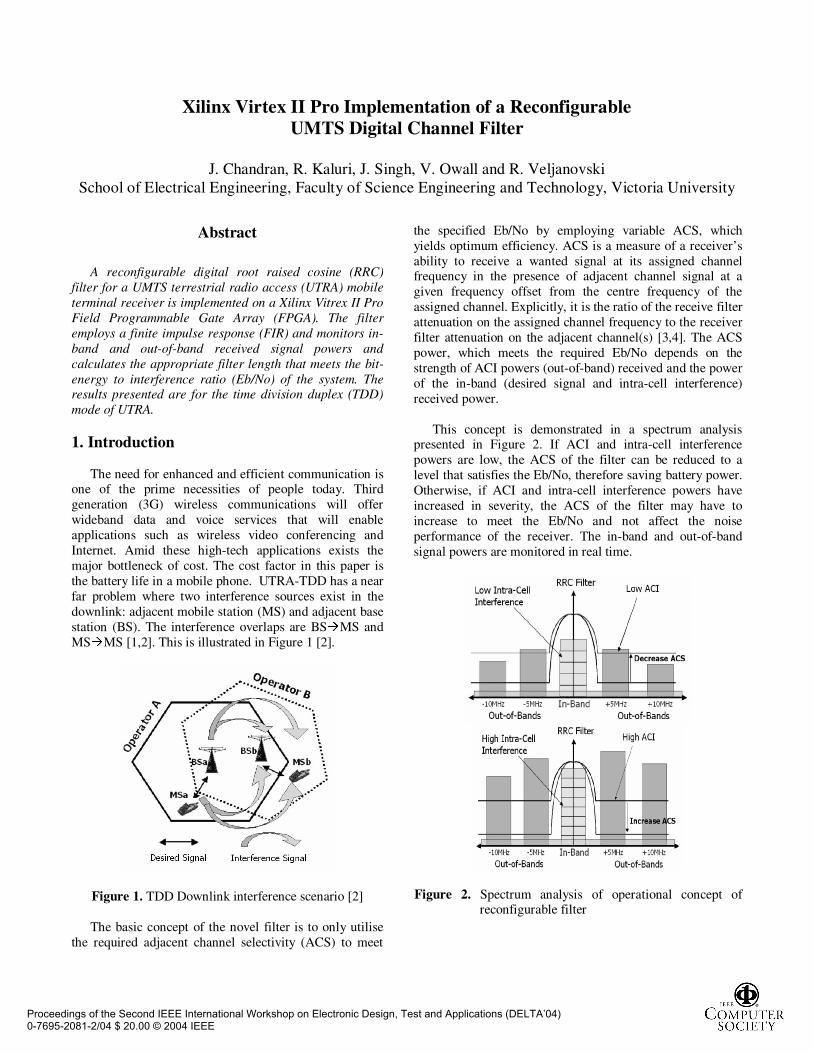
The need for enhanced and efficient communication is one of the prime necessities of people today. Third generation (3G) wireless communications will offer wideband data and voice services that will enable applications such as wireless video conferencing and Internet. Amid these high-tech applications exists the major bottleneck of cost. The cost factor in this paper is the battery life in a mobile phone. UTRA-TDD has a near far problem where two interference sources exist in the downlink: adjacent mobile station (MS) and adjacent base station (BS). The interference overlaps are BS�MS and MS�MS [1,2]. This is illustrated in Figure 1 [2].
Figure 1. TDD Downlink interference scenario [2]
The basic concept of the novel filter is to only utilise the required adjacent channel selectivity (ACS) to meet
the specified Eb/No by employing variable ACS, which yields optimum efficiency. ACS is a measure of a receiver’s ability to receive a wanted signal at its assigned channel frequency in the presence of adjacent channel signal at a given frequency offset from the centre frequency of the assigned channel. Explicitly, it is the ratio of the receive filter attenuation on the assigned channel frequency to the receiver filter attenuation on the adjacent channel(s) [3,4]. The ACS power, which meets the required Eb/No depends on the strength of ACI powers (out-of-band) received and the power of the in-band (desired signal and intra-cell interference) received power.
This concept is demonstrated in a spectrum analysis presented in Figure 2. If ACI and intra-cell interference powers are low, the ACS of the filter can be reduced to a level that satisfies the Eb/No, therefore saving battery power. Otherwise, if ACI and intra-cell interference powers have increased in severity, the ACS of the filter may have to increase to meet the Eb/No and not affect the noise performance of the receiver. The in-band and out-of-band signal powers are monitored in real time.
Figure 2. Spectrum analysis of operational concept of reconfigurable filter
Proceedings of the Second IEEE International Workshop on Electronic Design, Test and Applications (DELTA’04) 0-7695-2081-2/04 $ 20.00 © 2004 IEEE
2. Reconfigurable Architecture
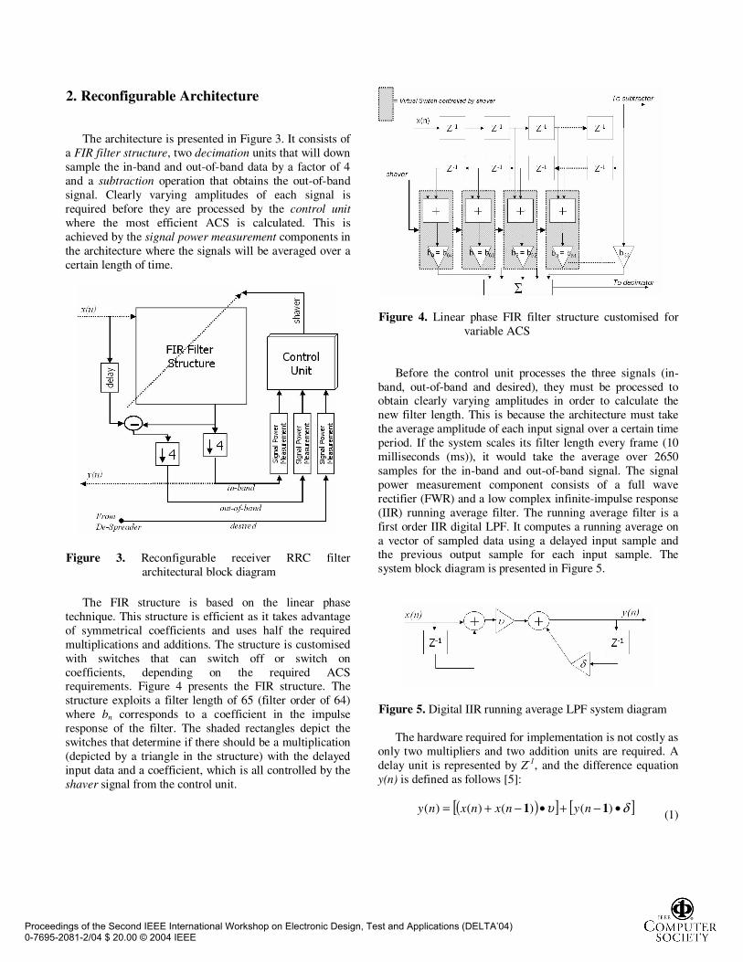
The architecture is presented in Figure 3. It consists of a FIR filter structure, two decimation units that will down sample the in-band and out-of-band data by a factor of 4 and a subtraction operation that obtains the out-of-band signal. Clearly varying amplitudes of each signal is required before they are processed by the control unitwhere the most efficient ACS is calculated. This is achieved by the signal power measurement components in the architecture where the signals will be averaged over a certain length of time.
Figure 3. Reconfigurable receiver RRC filter architectural block diagram
The FIR structure is based on the linear phase technique. This structure is efficient as it takes advantage of symmetrical coefficients and uses half the required multiplications and additions. The structure is customised with switches that can switch off or switch on coefficients, depending on the required ACS requirements. Figure 4 presents the FIR structure. The structure exploits a filter length of 65 (filter order of 64) where bn corresponds to a coefficient in the impulse response of the filter. The shaded rectangles depict the switches that determine if there should be a multiplication (depicted by a triangle in the structure) with the delayed input data and a coefficient, which is all controlled by the shaver signal from the control unit.
Figure 4. Linear phase FIR filter structure customised for variable ACS
Before the control unit processes the three signals (in-band, out-of-band and desired), they must be processed to obtain clearly varying amplitudes in order to calculate the new filter length. This is because the architecture must take the average amplitude of each input signal over a certain time period. If the system scales its filter length every frame (10 milliseconds (ms)), it would take the average over 2650 samples for the in-band and out-of-band signal. The signal power measurement component consists of a full wave rectifier (FWR) and a low complex infinite-impulse response (IIR) running average filter. The running average filter is a first order IIR digital LPF. It computes a running average on a vector of sampled data using a delayed input sample and the previous output sample for each input sample. The system block diagram is presented in Figure 5.
Figure 5. Digital IIR running average LPF system diagram
The hardware required for implementation is not costly as only two multipliers and two addition units are required. A delay unit is represented by Z-1, and the difference equation y(n) is defined as follows [5]:
( )[ ] [ ]δυ •−+•−+= )()()()( 11 nynxnxny (1)
Proceedings of the Second IEEE International Workshop on Electronic Design, Test and Applications (DELTA’04) 0-7695-2081-2/04 $ 20.00 © 2004 IEEE
where x(n) is the current input sample, x(n-1) is a delayed input sample, y(n-1) is a delayed output sample, and υ is defined as [5]:
( )2
1 δυ −= (2)
δ is described as follows [5]:
c
c
θθδ
sin
cos
+=
1 (3)
where θc is a normalised frequency of 0.002π [5].
The control unit is the intelligence behind the architecture. It calculates the appropriate filter length based on the three signals and adjusts the filter length by shaving off or adding taps to the ends of the impulse response. This lowers or raises the ACS dB level. The algorithm for the control unit has been previously derived in literature [6,7].
3. Filter Design
The reconfigurable was implemented with a semi custom digital design methodology. The filer design was implemented in Register Transfer Level (RTL) and behavioural style of coding. The RTL style of coding employs building of small blocks in behavioural coding and uses these blocks to build the complete circuits. In behavioural style the whole code is coded according to the behaviour of the circuit. The filter architecture was implemented in FPGA and the Xilinx Virtex II PRO was selected for implementation. The filter architecture was also implemented in semi-custom application specific integrated circuit (ASIC). The ASIC and FPGA were coded in VHDL – behavioral and RTL. They were synthesized in Synopsys Design Compiler and synthesized in FPGA Compiler II. Educational digital libraries were used for the ASIC implementation.
3.1 RTL Design
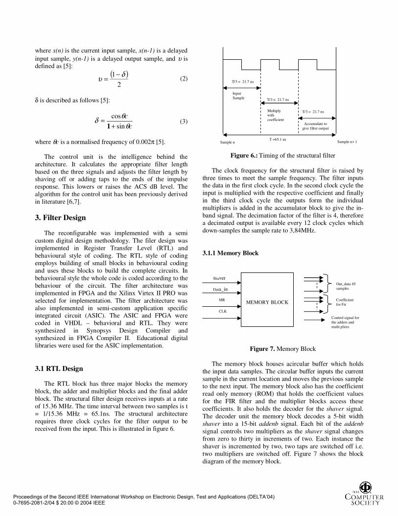
The RTL block has three major blocks the memory block, the adder and multiplier blocks and the final adder block. The structural filter design receives inputs at a rate of 15.36 MHz. The time interval between two samples is t = 1/15.36 MHz = 65.1ns. The structural architecture requires three clock cycles for the filter output to be received from the input. This is illustrated in figure 6.
Figure 6.: Timing of the structural filter
The clock frequency for the structural filter is raised by three times to meet the sample frequency. The filter inputs the data in the first clock cycle. In the second clock cycle the input is multiplied with the respective coefficient and finally in the third clock cycle the outputs form the individual multipliers is added in the accumulator block to give the in-band signal. The decimation factor of the filter is 4, therefore a decimated output is available every 12 clock cycles which down-samples the sample rate to 3,84MHz.
3.1.1 Memory Block
Figure 7. Memory Block
The memory block houses acircular buffer which holds the input data samples. The circular buffer inputs the current sample in the current location and moves the previous sample to the next input. The memory block also has the coefficient read only memory (ROM) that holds the coefficient values for the FIR filter and the multiplier blocks access these coefficients. It also holds the decoder for the shaver signal. The decoder unit the memory block decodes a 5-bit width shaver into a 15-bit addenb signal. Each bit of the addenbsignal controls two multipliers as the shaver signal changes from zero to thirty in increments of two. Each instance the shaver is incremented by two, two taps are switched off i.e. two multipliers are switched off. Figure 7 shows the block diagram of the memory block.
Sample n+ 1T =65.1 ns
T/3 = 21.7 ns
T/3 = 21.7 ns
T/3 = 21.7 ns
Sample n
Input Sample
Multiply with coefficient
Accumulate to give filter output
MEMORY BLOCK
Shaver
Data_in
MR
CLK
Out_data 65samples
Coefficient for Fir
Control signal for the adders and multi pliers
Proceedings of the Second IEEE International Workshop on Electronic Design, Test and Applications (DELTA’04) 0-7695-2081-2/04 $ 20.00 © 2004 IEEE
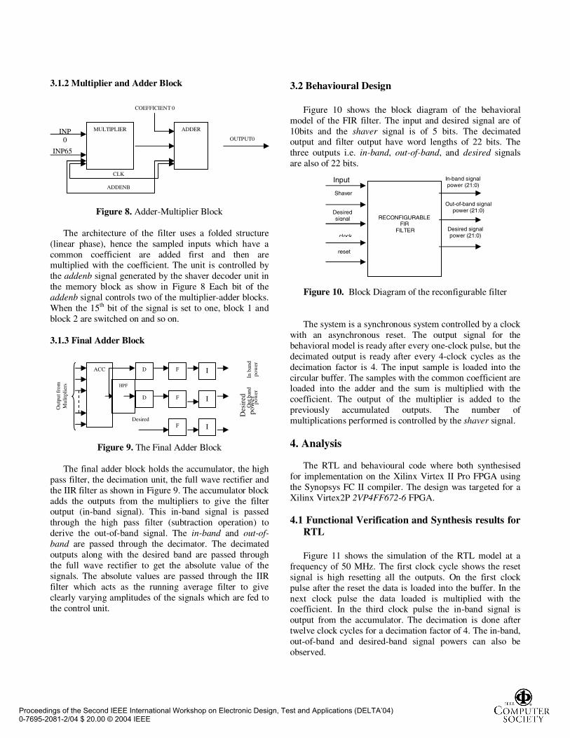
3.1.2 Multiplier and Adder Block
Figure 8. Adder-Multiplier Block
The architecture of the filter uses a folded structure (linear phase), hence the sampled inputs which have a common coefficient are added first and then are multiplied with the coefficient. The unit is controlled by the addenb signal generated by the shaver decoder unit in the memory block as show in Figure 8 Each bit of the addenb signal controls two of the multiplier-adder blocks. When the 15th bit of the signal is set to one, block 1 and block 2 are switched on and so on.
3.1.3 Final Adder Block
Figure 9. The Final Adder Block
The final adder block holds the accumulator, the high pass filter, the decimation unit, the full wave rectifier and the IIR filter as shown in Figure 9. The accumulator block adds the outputs from the multipliers to give the filter output (in-band signal). This in-band signal is passed through the high pass filter (subtraction operation) to derive the out-of-band signal. The in-band and out-of-band are passed through the decimator. The decimated outputs along with the desired band are passed through the full wave rectifier to get the absolute value of the signals. The absolute values are passed through the IIR filter which acts as the running average filter to give clearly varying amplitudes of the signals which are fed to the control unit.
3.2 Behavioural Design
Figure 10 shows the block diagram of the behavioral model of the FIR filter. The input and desired signal are of 10bits and the shaver signal is of 5 bits. The decimated output and filter output have word lengths of 22 bits. The three outputs i.e. in-band, out-of-band, and desired signals are also of 22 bits.
Figure 10. Block Diagram of the reconfigurable filter
The system is a synchronous system controlled by a clock with an asynchronous reset. The output signal for the behavioral model is ready after every one-clock pulse, but the decimated output is ready after every 4-clock cycles as the decimation factor is 4. The input sample is loaded into the circular buffer. The samples with the common coefficient are loaded into the adder and the sum is multiplied with the coefficient. The output of the multiplier is added to the previously accumulated outputs. The number of multiplications performed is controlled by the shaver signal.
4. Analysis
The RTL and behavioural code where both synthesised for implementation on the Xilinx Virtex II Pro FPGA using the Synopsys FC II compiler. The design was targeted for a Xilinx Virtex2P 2VP4FF672-6 FPGA.
4.1 Functional Verification and Synthesis results for RTL
Figure 11 shows the simulation of the RTL model at a frequency of 50 MHz. The first clock cycle shows the reset signal is high resetting all the outputs. On the first clock pulse after the reset the data is loaded into the buffer. In the next clock pulse the data loaded is multiplied with the coefficient. In the third clock pulse the in-band signal is output from the accumulator. The decimation is done after twelve clock cycles for a decimation factor of 4. The in-band, out-of-band and desired-band signal powers can also be observed.
MULTIPLIER ADDERINP0
INP65
CLK
ADDENB
COEFFICIENT 0
OUTPUT0
In b
and
pow
er
ACC D
D
HPF
F
F
F
I
I
I
Out
put f
rom
M
ulit
plie
rs
Desired
Out
ban
d po
wer
Des
ired
po
wer
RECONFIGURABLE FIR
FILTER
Input
Shaver
Desired signal
clock
reset
In-band signal power (21:0)
Out-of-band signal power (21:0)
Desired signal power (21:0)
Proceedings of the Second IEEE International Workshop on Electronic Design, Test and Applications (DELTA’04) 0-7695-2081-2/04 $ 20.00 © 2004 IEEE
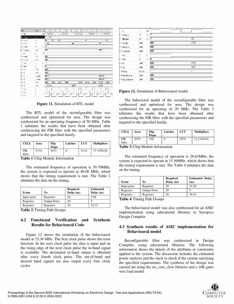
Figure 11. Simulation of RTL model
The RTL model of the reconfigurable filter was synthesized and optimized for area. The design was synthesised for an operating frequency of 50 MHz. Table 1 tabulates the results that have been obtained after synthesizing the FIR filter with the specified parameters and targeted to the specified family.
CELL Area Flip Flops
Latches LUT Multipliers
FIR filter
5114 1631 0 5114 17 (18X18)
Table 1: Chip Module Information
The estimated frequency of operation is 59.70MHz; the system is expected to operate at 46.08 MHz, which shows that the timing requirement is met. The Table 2 tabulates the data on the timing.
From To Required Delay (ns)
Estimated Delay (ns)
Input ports Registers 20 5.98 Registers Output Ports 20 5 Registers Registers 20 16.75
Table 2: Timing Path Groups
4.2 Functional Verification and Synthesis Results for Behavioural Code
Figure 12 shows the simulation of the behavioural model at 15.36 MHz. The first clock pulse shows the reset function. In the next clock pulse the data is input and on the rising edge of the next clock pulse the in-band signal is available. The decimated in-band output is obtained after every fourth clock pulse. The out-of-band and desired band signals are also output every four clock cycles.
Figure 12. Simulation of Behavioural model
The behavioral model of the reconfigurable filter was synthesized and optimized for area. The design was synthesised for an operating of 20 MHz. The Table 3 tabulates the results that have been obtained after synthesizing the FIR filter with the specified parameters and targeted to the specified family.
CELL Area Flip Flops
Latches LUT Multipliers
FIR filter
2079 760 0 2079 12 (18X18)
Table 3: Chip Module Information
The estimated frequency of operation is 28.63MHz; the system is expected to operate at 15.36MHz, which shows that the timing requirement is met. The Table 4 tabulates the data on the timing.
From To Required Delay (ns)
Estimated Delay (ns)
Input ports Registers 50 34.20 Registers Output Ports 50 5 Registers Registers 50 34.93
Table 4: Timing Path Groups
The behavioural model was also synthesised for an ASIC implementation using educational libraries in Synopsys Design Compiler.
4.3 Synthesis results of ASIC implementation for Behavioural model
Reconfigurable filter was synthesized in Design Compiler, using educational libraries. The following information shows the details of the attributes or constraints applied to the system. The discussion includes the estimated power analysis and the slack to check if the system satisfying the specified requirements. The synthesis of the design was carried out using the ssc_core_slow libraries and a 10K gates wire load model.
Proceedings of the Second IEEE International Workshop on Electronic Design, Test and Applications (DELTA’04) 0-7695-2081-2/04 $ 20.00 © 2004 IEEE
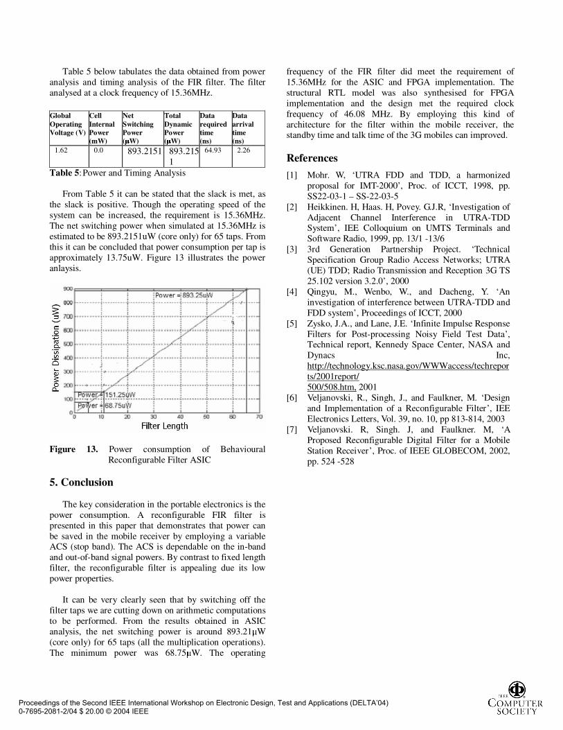
Table 5 below tabulates the data obtained from power analysis and timing analysis of the FIR filter. The filter analysed at a clock frequency of 15.36MHz.
Global Operating Voltage (V)
Cell InternalPower(mW)
Net Switching Power (µW)
Total Dynamic Power (µW)
Data required time (ns)
Data arrival time(ns)
1.62 0.0 893.2151 893.2151
64.93 2.26
Table 5: Power and Timing Analysis
From Table 5 it can be stated that the slack is met, as the slack is positive. Though the operating speed of the system can be increased, the requirement is 15.36MHz. The net switching power when simulated at 15.36MHz is estimated to be 893.2151uW (core only) for 65 taps. From this it can be concluded that power consumption per tap is approximately 13.75uW. Figure 13 illustrates the power anlaysis.
Figure 13. Power consumption of Behavioural Reconfigurable Filter ASIC
5. Conclusion
The key consideration in the portable electronics is the power consumption. A reconfigurable FIR filter is presented in this paper that demonstrates that power can be saved in the mobile receiver by employing a variable ACS (stop band). The ACS is dependable on the in-band and out-of-band signal powers. By contrast to fixed length filter, the reconfigurable filter is appealing due its low power properties.
It can be very clearly seen that by switching off the filter taps we are cutting down on arithmetic computations to be performed. From the results obtained in ASIC analysis, the net switching power is around 893.21µW(core only) for 65 taps (all the multiplication operations). The minimum power was 68.75µW. The operating
frequency of the FIR filter did meet the requirement of 15.36MHz for the ASIC and FPGA implementation. The structural RTL model was also synthesised for FPGA implementation and the design met the required clock frequency of 46.08 MHz. By employing this kind of architecture for the filter within the mobile receiver, the standby time and talk time of the 3G mobiles can improved.
References
[1] Mohr. W, ‘UTRA FDD and TDD, a harmonized proposal for IMT-2000’, Proc. of ICCT, 1998, pp. SS22-03-1 – SS-22-03-5
[2] Heikkinen. H, Haas. H, Povey. G.J.R, ‘Investigation of Adjacent Channel Interference in UTRA-TDD System’, IEE Colloquium on UMTS Terminals and Software Radio, 1999, pp. 13/1 -13/6
[3] 3rd Generation Partnership Project. ‘Technical Specification Group Radio Access Networks; UTRA (UE) TDD; Radio Transmission and Reception 3G TS 25.102 version 3.2.0’, 2000
[4] Qingyu, M., Wenbo, W., and Dacheng, Y. ‘An investigation of interference between UTRA-TDD and FDD system’, Proceedings of ICCT, 2000
[5] Zysko, J.A., and Lane, J.E. ‘Infinite Impulse Response Filters for Post-processing Noisy Field Test Data’, Technical report, Kennedy Space Center, NASA and Dynacs Inc, http://technology.ksc.nasa.gov/WWWaccess/techreports/2001report/500/508.htm, 2001
[6] Veljanovski, R., Singh, J., and Faulkner, M. ‘Design and Implementation of a Reconfigurable Filter’, IEE Electronics Letters, Vol. 39, no. 10, pp 813-814, 2003
[7] Veljanovski. R, Singh. J, and Faulkner. M, ‘A Proposed Reconfigurable Digital Filter for a Mobile Station Receiver’, Proc. of IEEE GLOBECOM, 2002, pp. 524 -528
Proceedings of the Second IEEE International Workshop on Electronic Design, Test and Applications (DELTA’04) 0-7695-2081-2/04 $ 20.00 © 2004 IEEE