Embed Size (px)
Citation preview
FN8566Rev 1.00
November 2, 2015
ISL95712Multiphase PWM Regulator for AMD Fusion™ Desktop CPUs Using SVI 2.0
DATASHEET
The ISL95712 is fully compliant with AMD Fusion™ SVI 2.0 and provides a complete solution for microprocessor and graphics processor core power. The ISL95712 controller supports two Voltage Regulators (VRs) for Core and Northbridge outputs. The Core VR can be configured for 4-, 3-, 2-, or 1-phase operation while the Northbridge VR supports 3-, 2- or 1-phase configurations for maximum flexibility. The two VRs share a serial control bus to communicate with the AMD CPU and achieve lower cost and smaller board area compared with two-chip solutions.
The PWM modulator is based on Intersil’s Robust Ripple Regulator R3™ Technology. Compared to traditional modulators, the R3™ modulator can automatically change switching frequency for faster transient settling time during load transients and improved light load efficiency.
The ISL95712 has several other key features. Both outputs support DCR current sensing with a single NTC thermistor for DCR temperature compensation or accurate resistor current sensing. They also utilize remote voltage sense, adjustable switching frequency, OC protection and power-good indicators.
Applications• AMD Fusion CPU/GPU core power
• Desktop computers
Features• Supports AMD SVI 2.0 serial data bus interface and PMBus
- Serial VID clock frequency range 100kHz to 25MHz
• Dual output controller with 12V integrated core gate drivers
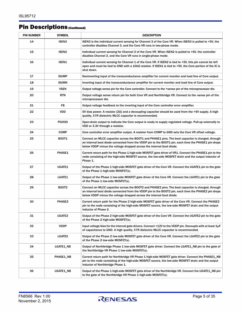
• Precision voltage regulation
- 0.5% system accuracy over-temperature
- 0.5V to 1.55V in 6.25mV steps
- Enhanced load line accuracy
• Supports multiple current sensing methods
- Lossless inductor DCR current sensing
- Precision resistor current sensing
• Programmable 1-, 2-, 3- or 4-phase for the core output and 1- , 2- or 3-phase for the Northbridge output
• Adaptive body diode conduction time reduction
• Superior noise immunity and transient response
• Output current and voltage telemetry
• Differential remote voltage sensing
• High efficiency across entire load range
• Programmable slew rate
• Programmable VID offset and droop on both outputs
• Programmable switching frequency for both outputs
• Excellent dynamic current balance between phases
• Protection: OCP/WOC, OVP, PGOOD and thermal monitor
• Small footprint 52 Ld 6x6 QFN package
- Pb-free (RoHS compliant)
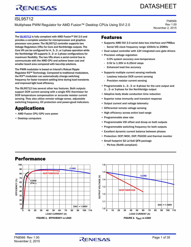
Performance
FIGURE 1. EFFICIENCY vs LOAD FIGURE 2. VOUT vs LOAD
0
10
20
30
40
50
60
70
80
90
100
0 10 20 30 40 50 60 70 80 90 100 110
EF
FIC
IEN
CY
(%
)
LOAD CURRENT (A)
DAC = 1.500V
NORTHBRIDGE
CORE
CORE (PSI1)
1.0
1.1
1.2
1.3
1.4
1.5
1.6
0 10 20 30 40 50 60 70 80 90 100 110
OU
TP
UT
VO
LT
AG
E (
V)
LOAD CURRENT (A)
DAC = 1.500V
NORTHBRIDGE
CORE
FN8566 Rev 1.00 Page 1 of 35November 2, 2015
ISL95712
Table of ContentsSimplified Application Circuit for High Power CPU Core. . . . . . . . . . . . . . . . . . . . . . . . . . . . . . . . . . . . . . . . . . . . . . . . . . . . . . . . . . . 3Pin Configuration. . . . . . . . . . . . . . . . . . . . . . . . . . . . . . . . . . . . . . . . . . . . . . . . . . . . . . . . . . . . . . . . . . . . . . . . . . . . . . . . . . . . . . . . . . . . 4Pin Descriptions. . . . . . . . . . . . . . . . . . . . . . . . . . . . . . . . . . . . . . . . . . . . . . . . . . . . . . . . . . . . . . . . . . . . . . . . . . . . . . . . . . . . . . . . . . . . . 4Ordering Information . . . . . . . . . . . . . . . . . . . . . . . . . . . . . . . . . . . . . . . . . . . . . . . . . . . . . . . . . . . . . . . . . . . . . . . . . . . . . . . . . . . . . . . . 6Absolute Maximum Ratings . . . . . . . . . . . . . . . . . . . . . . . . . . . . . . . . . . . . . . . . . . . . . . . . . . . . . . . . . . . . . . . . . . . . . . . . . . . . . . . . . . . 7Thermal Information . . . . . . . . . . . . . . . . . . . . . . . . . . . . . . . . . . . . . . . . . . . . . . . . . . . . . . . . . . . . . . . . . . . . . . . . . . . . . . . . . . . . . . . . . 7Recommended Operating Conditions . . . . . . . . . . . . . . . . . . . . . . . . . . . . . . . . . . . . . . . . . . . . . . . . . . . . . . . . . . . . . . . . . . . . . . . . . . 7Electrical Specifications . . . . . . . . . . . . . . . . . . . . . . . . . . . . . . . . . . . . . . . . . . . . . . . . . . . . . . . . . . . . . . . . . . . . . . . . . . . . . . . . . . . . . 7Gate Driver Timing Diagram . . . . . . . . . . . . . . . . . . . . . . . . . . . . . . . . . . . . . . . . . . . . . . . . . . . . . . . . . . . . . . . . . . . . . . . . . . . . . . . . . . . 9Theory of Operation. . . . . . . . . . . . . . . . . . . . . . . . . . . . . . . . . . . . . . . . . . . . . . . . . . . . . . . . . . . . . . . . . . . . . . . . . . . . . . . . . . . . . . . . . 10
Multiphase R3™ Modulator . . . . . . . . . . . . . . . . . . . . . . . . . . . . . . . . . . . . . . . . . . . . . . . . . . . . . . . . . . . . . . . . . . . . . . . . . . . . . . . . . . . . . . . 10Diode Emulation and Period Stretching . . . . . . . . . . . . . . . . . . . . . . . . . . . . . . . . . . . . . . . . . . . . . . . . . . . . . . . . . . . . . . . . . . . . . . . . . . . . . 11Channel Configuration . . . . . . . . . . . . . . . . . . . . . . . . . . . . . . . . . . . . . . . . . . . . . . . . . . . . . . . . . . . . . . . . . . . . . . . . . . . . . . . . . . . . . . . . . . . 11Power-On Reset . . . . . . . . . . . . . . . . . . . . . . . . . . . . . . . . . . . . . . . . . . . . . . . . . . . . . . . . . . . . . . . . . . . . . . . . . . . . . . . . . . . . . . . . . . . . . . . . . 11Start-Up Timing . . . . . . . . . . . . . . . . . . . . . . . . . . . . . . . . . . . . . . . . . . . . . . . . . . . . . . . . . . . . . . . . . . . . . . . . . . . . . . . . . . . . . . . . . . . . . . . . . 12Diode Throttling . . . . . . . . . . . . . . . . . . . . . . . . . . . . . . . . . . . . . . . . . . . . . . . . . . . . . . . . . . . . . . . . . . . . . . . . . . . . . . . . . . . . . . . . . . . . . . . . . 12Voltage Regulation and Load Line Implementation . . . . . . . . . . . . . . . . . . . . . . . . . . . . . . . . . . . . . . . . . . . . . . . . . . . . . . . . . . . . . . . . . . . 12Differential Sensing. . . . . . . . . . . . . . . . . . . . . . . . . . . . . . . . . . . . . . . . . . . . . . . . . . . . . . . . . . . . . . . . . . . . . . . . . . . . . . . . . . . . . . . . . . . . . . 13Phase Current Balancing . . . . . . . . . . . . . . . . . . . . . . . . . . . . . . . . . . . . . . . . . . . . . . . . . . . . . . . . . . . . . . . . . . . . . . . . . . . . . . . . . . . . . . . . . 13Modes of Operation . . . . . . . . . . . . . . . . . . . . . . . . . . . . . . . . . . . . . . . . . . . . . . . . . . . . . . . . . . . . . . . . . . . . . . . . . . . . . . . . . . . . . . . . . . . . . . 15Dynamic Operation . . . . . . . . . . . . . . . . . . . . . . . . . . . . . . . . . . . . . . . . . . . . . . . . . . . . . . . . . . . . . . . . . . . . . . . . . . . . . . . . . . . . . . . . . . . . . . 16Adaptive Body Diode Conduction Time Reduction . . . . . . . . . . . . . . . . . . . . . . . . . . . . . . . . . . . . . . . . . . . . . . . . . . . . . . . . . . . . . . . . . . . . 16
Resistor Configuration Options. . . . . . . . . . . . . . . . . . . . . . . . . . . . . . . . . . . . . . . . . . . . . . . . . . . . . . . . . . . . . . . . . . . . . . . . . . . . . . . 16VR Offset Programming . . . . . . . . . . . . . . . . . . . . . . . . . . . . . . . . . . . . . . . . . . . . . . . . . . . . . . . . . . . . . . . . . . . . . . . . . . . . . . . . . . . . . . . . . . 16VID-on-the-Fly Slew Rate Selection . . . . . . . . . . . . . . . . . . . . . . . . . . . . . . . . . . . . . . . . . . . . . . . . . . . . . . . . . . . . . . . . . . . . . . . . . . . . . . . . . 17CCM Switching Frequency . . . . . . . . . . . . . . . . . . . . . . . . . . . . . . . . . . . . . . . . . . . . . . . . . . . . . . . . . . . . . . . . . . . . . . . . . . . . . . . . . . . . . . . . 17
AMD Serial VID Interface 2.0 . . . . . . . . . . . . . . . . . . . . . . . . . . . . . . . . . . . . . . . . . . . . . . . . . . . . . . . . . . . . . . . . . . . . . . . . . . . . . . . . . 17Pre-PWROK Metal VID. . . . . . . . . . . . . . . . . . . . . . . . . . . . . . . . . . . . . . . . . . . . . . . . . . . . . . . . . . . . . . . . . . . . . . . . . . . . . . . . . . . . . . . . . . . . 17SVI Interface Active . . . . . . . . . . . . . . . . . . . . . . . . . . . . . . . . . . . . . . . . . . . . . . . . . . . . . . . . . . . . . . . . . . . . . . . . . . . . . . . . . . . . . . . . . . . . . . 18VID-on-the-Fly Transition . . . . . . . . . . . . . . . . . . . . . . . . . . . . . . . . . . . . . . . . . . . . . . . . . . . . . . . . . . . . . . . . . . . . . . . . . . . . . . . . . . . . . . . . . . 18SVI Data Communication Protocol . . . . . . . . . . . . . . . . . . . . . . . . . . . . . . . . . . . . . . . . . . . . . . . . . . . . . . . . . . . . . . . . . . . . . . . . . . . . . . . . . 18SVI Bus Protocol. . . . . . . . . . . . . . . . . . . . . . . . . . . . . . . . . . . . . . . . . . . . . . . . . . . . . . . . . . . . . . . . . . . . . . . . . . . . . . . . . . . . . . . . . . . . . . . . . 21Power States . . . . . . . . . . . . . . . . . . . . . . . . . . . . . . . . . . . . . . . . . . . . . . . . . . . . . . . . . . . . . . . . . . . . . . . . . . . . . . . . . . . . . . . . . . . . . . . . . . . 21Dynamic Load Line Slope Trim . . . . . . . . . . . . . . . . . . . . . . . . . . . . . . . . . . . . . . . . . . . . . . . . . . . . . . . . . . . . . . . . . . . . . . . . . . . . . . . . . . . . 22Dynamic Offset Trim . . . . . . . . . . . . . . . . . . . . . . . . . . . . . . . . . . . . . . . . . . . . . . . . . . . . . . . . . . . . . . . . . . . . . . . . . . . . . . . . . . . . . . . . . . . . . 22
Telemetry. . . . . . . . . . . . . . . . . . . . . . . . . . . . . . . . . . . . . . . . . . . . . . . . . . . . . . . . . . . . . . . . . . . . . . . . . . . . . . . . . . . . . . . . . . . . . . . . . . 22PMBus Interface . . . . . . . . . . . . . . . . . . . . . . . . . . . . . . . . . . . . . . . . . . . . . . . . . . . . . . . . . . . . . . . . . . . . . . . . . . . . . . . . . . . . . . . . . . . 23Protection Features. . . . . . . . . . . . . . . . . . . . . . . . . . . . . . . . . . . . . . . . . . . . . . . . . . . . . . . . . . . . . . . . . . . . . . . . . . . . . . . . . . . . . . . . . 24
Overcurrent . . . . . . . . . . . . . . . . . . . . . . . . . . . . . . . . . . . . . . . . . . . . . . . . . . . . . . . . . . . . . . . . . . . . . . . . . . . . . . . . . . . . . . . . . . . . . . . . . . . . . 24Current-Balance . . . . . . . . . . . . . . . . . . . . . . . . . . . . . . . . . . . . . . . . . . . . . . . . . . . . . . . . . . . . . . . . . . . . . . . . . . . . . . . . . . . . . . . . . . . . . . . . . 24Undervoltage . . . . . . . . . . . . . . . . . . . . . . . . . . . . . . . . . . . . . . . . . . . . . . . . . . . . . . . . . . . . . . . . . . . . . . . . . . . . . . . . . . . . . . . . . . . . . . . . . . . 25Overvoltage. . . . . . . . . . . . . . . . . . . . . . . . . . . . . . . . . . . . . . . . . . . . . . . . . . . . . . . . . . . . . . . . . . . . . . . . . . . . . . . . . . . . . . . . . . . . . . . . . . . . . 25Thermal Monitor [NTC, NTC_NB] . . . . . . . . . . . . . . . . . . . . . . . . . . . . . . . . . . . . . . . . . . . . . . . . . . . . . . . . . . . . . . . . . . . . . . . . . . . . . . . . . . . 25Fault Recovery . . . . . . . . . . . . . . . . . . . . . . . . . . . . . . . . . . . . . . . . . . . . . . . . . . . . . . . . . . . . . . . . . . . . . . . . . . . . . . . . . . . . . . . . . . . . . . . . . . 26Interface Pin Protection . . . . . . . . . . . . . . . . . . . . . . . . . . . . . . . . . . . . . . . . . . . . . . . . . . . . . . . . . . . . . . . . . . . . . . . . . . . . . . . . . . . . . . . . . . 26
Key Component Selection . . . . . . . . . . . . . . . . . . . . . . . . . . . . . . . . . . . . . . . . . . . . . . . . . . . . . . . . . . . . . . . . . . . . . . . . . . . . . . . . . . . 26Inductor DCR Current-Sensing Network . . . . . . . . . . . . . . . . . . . . . . . . . . . . . . . . . . . . . . . . . . . . . . . . . . . . . . . . . . . . . . . . . . . . . . . . . . . . . 26Resistor Current-Sensing Network . . . . . . . . . . . . . . . . . . . . . . . . . . . . . . . . . . . . . . . . . . . . . . . . . . . . . . . . . . . . . . . . . . . . . . . . . . . . . . . . . 28Overcurrent Protection . . . . . . . . . . . . . . . . . . . . . . . . . . . . . . . . . . . . . . . . . . . . . . . . . . . . . . . . . . . . . . . . . . . . . . . . . . . . . . . . . . . . . . . . . . . 28Load Line Slope . . . . . . . . . . . . . . . . . . . . . . . . . . . . . . . . . . . . . . . . . . . . . . . . . . . . . . . . . . . . . . . . . . . . . . . . . . . . . . . . . . . . . . . . . . . . . . . . . 29Compensator . . . . . . . . . . . . . . . . . . . . . . . . . . . . . . . . . . . . . . . . . . . . . . . . . . . . . . . . . . . . . . . . . . . . . . . . . . . . . . . . . . . . . . . . . . . . . . . . . . . 29Current Balancing . . . . . . . . . . . . . . . . . . . . . . . . . . . . . . . . . . . . . . . . . . . . . . . . . . . . . . . . . . . . . . . . . . . . . . . . . . . . . . . . . . . . . . . . . . . . . . . 30Thermal Monitor Component Selection . . . . . . . . . . . . . . . . . . . . . . . . . . . . . . . . . . . . . . . . . . . . . . . . . . . . . . . . . . . . . . . . . . . . . . . . . . . . . 30
Layout Guidelines . . . . . . . . . . . . . . . . . . . . . . . . . . . . . . . . . . . . . . . . . . . . . . . . . . . . . . . . . . . . . . . . . . . . . . . . . . . . . . . . . . . . . . . . . . 31PCB Layout Considerations . . . . . . . . . . . . . . . . . . . . . . . . . . . . . . . . . . . . . . . . . . . . . . . . . . . . . . . . . . . . . . . . . . . . . . . . . . . . . . . . . . . . . . . 31
Revision History. . . . . . . . . . . . . . . . . . . . . . . . . . . . . . . . . . . . . . . . . . . . . . . . . . . . . . . . . . . . . . . . . . . . . . . . . . . . . . . . . . . . . . . . . . . . 34About Intersil . . . . . . . . . . . . . . . . . . . . . . . . . . . . . . . . . . . . . . . . . . . . . . . . . . . . . . . . . . . . . . . . . . . . . . . . . . . . . . . . . . . . . . . . . . . . . . 34
Package Outline Drawing . . . . . . . . . . . . . . . . . . . . . . . . . . . . . . . . . . . . . . . . . . . . . . . . . . . . . . . . . . . . . . . . . . . . . . . . . . . . . . . . . . . . 35
FN8566 Rev 1.00 Page 2 of 35November 2, 2015
ISL95712
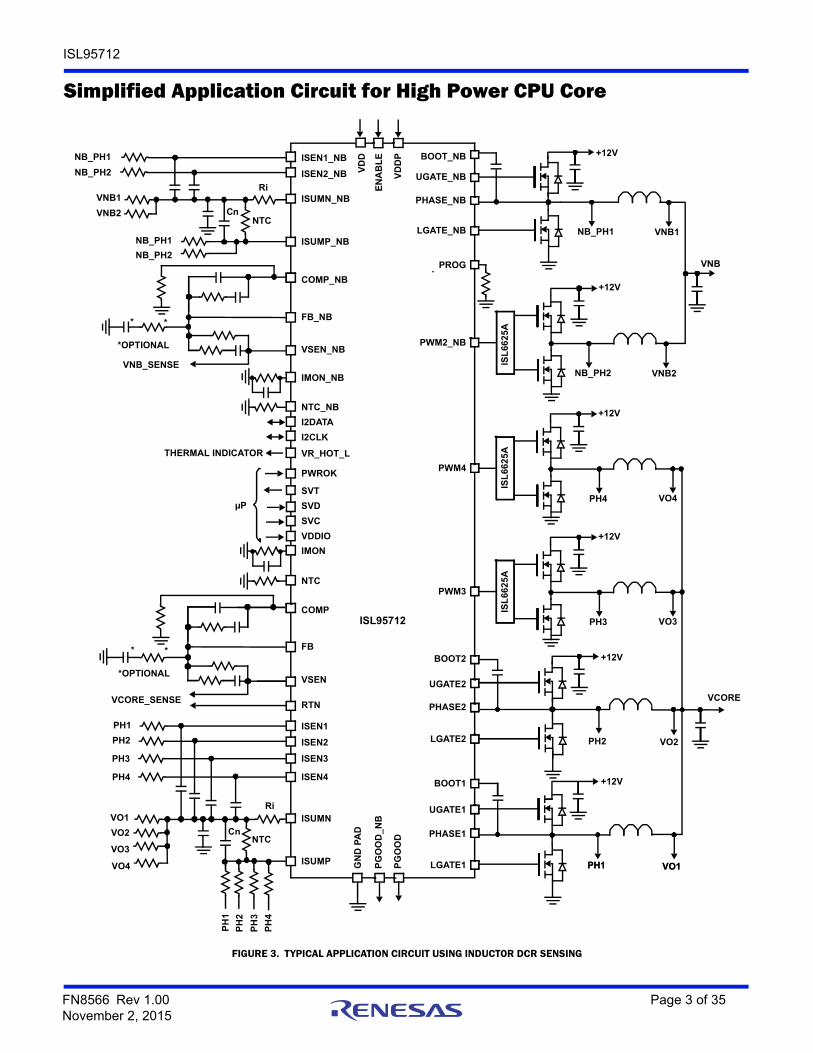
Simplified Application Circuit for High Power CPU Core
NB_PH1
NB_PH2
FIGURE 3. TYPICAL APPLICATION CIRCUIT USING INDUCTOR DCR SENSING
BOOT_NB
UGATE_NB
PHASE_NB
LGATE_NB
BOOT2
UGATE2
PHASE2
LGATE2
BOOT1
UGATE1
PHASE1
LGATE1
PWM3
ISUMP
ISUMN
PH
1
PH
2
PH
3
VO1
VO2
VO3
GN
D P
AD
FB_NB
COMP_NB
VSEN_NB
VNB_SENSE
VD
DP
PG
OO
D
ISEN1
ISEN2
ISEN3
EN
AB
LE
PH1
PH2
PH3
VCORE
PH2 VO2
VO1
+12V
VO3
PH1
+12V
+12V
VO1
PH3
PH1
+12V
VNB
VD
D
PWM2_NB
ISL
662
5A
VNB1NB_PH1
VNB2NB_PH2
ISEN1_NB
ISEN2_NB
ISUMP_NB
ISUMN_NB
NB_PH1
NB_PH2
VNB1
VNB2
NTC_NB
IMON
IMON_NB
PWROK
SVT
SVDµP
SVC
VDDIO
NTC
VR_HOT_LTHERMAL INDICATOR
PROG
VCORE_SENSE
FB
COMP
VSEN
RTN
+12V
NTC
NTC
Cn
Cn
Ri
Ri
*OPTIONAL
* *
*OPTIONAL
* *
ISEN4PH4
VO4
PH
4
PWM4
+12V
VO4PH4
PG
OO
D_
NB
ISL95712
I2DATA
I2CLK
ISL
662
5A
ISL
662
5A
FN8566 Rev 1.00 Page 3 of 35November 2, 2015
ISL95712
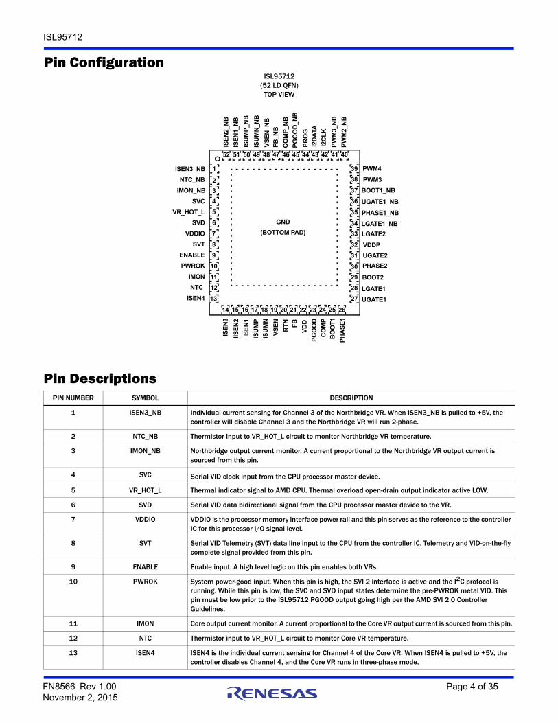
Pin ConfigurationISL95712
(52 LD QFN)TOP VIEW
1
52
GND
(BOTTOM PAD)
CO
MP
_NB
ISU
MP
_NB
2
3
NTC_NB
4SVC
5
6
VR_HOT_L
7
IMON
8
VDDIO
9
SVT
10
ENABLE
11
SVD
12NTC
51 50 49
VS
EN
_NB
48
PW
M3_
NB
47
PW
M2 _
NB
46 45 44
IMON_NB
43 42 41
PWM439
PWM338
37
PHASE1_NB
36
UGATE2
35
LGATE1_NB34
LGATE233
VDDP32
31
30
UGATE1_NB
29
PHASE2
28
BOOT1_NB
14
BO
OT
1
15
VS
EN
16
ISU
MN
17V
DD
18 19
FB
20 21 22
ISEN4
23 24
RT
N
PH
AS
E1
PWROK
ISU
MP
FB
_NB
ISU
MN
_NB
ISE
N1_
NB
LGATE1
IISE
N2
ISE
N1
ISE
N3
BOOT2
PR
OG
PG
OO
D_N
B
I2D
ATA
I2C
LK
PG
OO
D
40
27 UGATE113
25 26
ISEN3_NB
CO
MP
ISE
N2_
NB
Pin DescriptionsPIN NUMBER SYMBOL DESCRIPTION
1 ISEN3_NB Individual current sensing for Channel 3 of the Northbridge VR. When ISEN3_NB is pulled to +5V, the controller will disable Channel 3 and the Northbridge VR will run 2-phase.
2 NTC_NB Thermistor input to VR_HOT_L circuit to monitor Northbridge VR temperature.
3 IMON_NB Northbridge output current monitor. A current proportional to the Northbridge VR output current is sourced from this pin.
4 SVC Serial VID clock input from the CPU processor master device.
5 VR_HOT_L Thermal indicator signal to AMD CPU. Thermal overload open-drain output indicator active LOW.
6 SVD Serial VID data bidirectional signal from the CPU processor master device to the VR.
7 VDDIO VDDIO is the processor memory interface power rail and this pin serves as the reference to the controller IC for this processor I/O signal level.
8 SVT Serial VID Telemetry (SVT) data line input to the CPU from the controller IC. Telemetry and VID-on-the-fly complete signal provided from this pin.
9 ENABLE Enable input. A high level logic on this pin enables both VRs.
10 PWROK System power-good input. When this pin is high, the SVI 2 interface is active and the I2C protocol is running. While this pin is low, the SVC and SVD input states determine the pre-PWROK metal VID. This pin must be low prior to the ISL95712 PGOOD output going high per the AMD SVI 2.0 Controller Guidelines.
11 IMON Core output current monitor. A current proportional to the Core VR output current is sourced from this pin.
12 NTC Thermistor input to VR_HOT_L circuit to monitor Core VR temperature.
13 ISEN4 ISEN4 is the individual current sensing for Channel 4 of the Core VR. When ISEN4 is pulled to +5V, the controller disables Channel 4, and the Core VR runs in three-phase mode.
FN8566 Rev 1.00 Page 4 of 35November 2, 2015
ISL95712
14 ISEN3 ISEN3 is the individual current sensing for Channel 3 of the Core VR. When ISEN3 is pulled to +5V, the controller disables Channel 3, and the Core VR runs in two-phase mode.
15 ISEN2 Individual current sensing for Channel 2 of the Core VR. When ISEN2 is pulled to +5V, the controller disables Channel 2, and the Core VR runs in single-phase mode.
16 ISEN1 Individual current sensing for Channel 1 of the Core VR. If ISEN2 is tied to +5V, this pin cannot be left open and must be tied to GND with a 10kΩ resistor. If ISEN1 is tied to +5V, the Core portion of the IC is shut down.
17 ISUMP Noninverting input of the transconductance amplifier for current monitor and load line of Core output.
18 ISUMN Inverting input of the transconductance amplifier for current monitor and load line of Core output.
19 VSEN Output voltage sense pin for the Core controller. Connect to the +sense pin of the microprocessor die.
20 RTN Output voltage sense return pin for both Core VR and Northbridge VR. Connect to the -sense pin of the microprocessor die.
21 FB Output voltage feedback to the inverting input of the Core controller error amplifier.
22 VDD 5V bias power. A resistor [2Ω] and a decoupling capacitor should be used from the +5V supply. A high quality, X7R dielectric MLCC capacitor is recommended.
23 PGOOD Open-drain output to indicate the Core output is ready to supply regulated voltage. Pull-up externally to VDD or 3.3V through a resistor.
24 COMP Core controller error amplifier output. A resistor from COMP to GND sets the Core VR offset voltage.
25 BOOT1 Connect an MLCC capacitor across the BOOT1 and PHASE1 pins. The boot capacitor is charged, through an internal boot diode connected from the VDDP pin to the BOOT1 pin, each time the PHASE1 pin drops below VDDP minus the voltage dropped across the internal boot diode.
26 PHASE1 Current return path for the Phase 1 high-side MOSFET gate driver of VR1. Connect the PHASE1 pin to the node consisting of the high-side MOSFET source, the low-side MOSFET drain and the output inductor of Phase 1.
27 UGATE1 Output of the Phase 1 high-side MOSFET gate driver of the Core VR. Connect the UGATE1 pin to the gate of the Phase 1 high-side MOSFET(s).
28 LGATE1 Output of the Phase 1 low-side MOSFET gate driver of the Core VR. Connect the LGATE1 pin to the gate of the Phase 1 low-side MOSFET(s).
29 BOOT2 Connect an MLCC capacitor across the BOOT2 and PHASE2 pins. The boot capacitor is charged, through an internal boot diode connected from the VDDP pin to the BOOT2 pin, each time the PHASE2 pin drops below VDDP minus the voltage dropped across the internal boot diode.
30 PHASE2 Current return path for the Phase 2 high-side MOSFET gate driver of the Core VR. Connect the PHASE2 pin to the node consisting of the high-side MOSFET source, the low-side MOSFET drain and the output inductor of Phase 2.
31 UGATE2 Output of the Phase 2 high-side MOSFET gate driver of the Core VR. Connect the UGATE2 pin to the gate of the Phase 2 high-side MOSFET(s).
32 VDDP Input voltage bias for the internal gate drivers. Connect +12V to the VDDP pin. Decouple with at least 1µF of capacitance to GND. A high quality, X7R dielectric MLCC capacitor is recommended.
33 LGATE2 Output of the Phase 2 low-side MOSFET gate driver of the Core VR. Connect the LGATE2 pin to the gate of the Phase 2 low-side MOSFET(s).
34 LGATE1_NB Output of Northbridge Phase 1 low-side MOSFET gate driver. Connect the LGATE1_NB pin to the gate of the Northbridge VR Phase 1 low-side MOSFET(s).
35 PHASE1_NB Current return path for Northbridge VR Phase 1 high-side MOSFET gate driver. Connect the PHASE1_NB pin to the node consisting of the high-side MOSFET source, the low-side MOSFET drain and the output inductor of Northbridge Phase 1.
36 UGATE1_NB Output of the Phase 1 high-side MOSFET gate driver of the Northbridge VR. Connect the UGATE1_NB pin to the gate of the Northbridge VR Phase 1 high-side MOSFET(s).
Pin Descriptions (Continued)
PIN NUMBER SYMBOL DESCRIPTION
FN8566 Rev 1.00 Page 5 of 35November 2, 2015
ISL95712
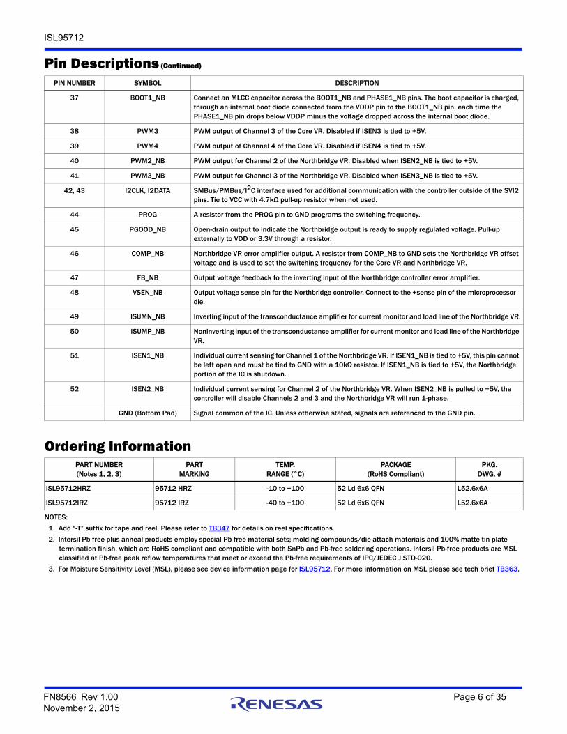
37 BOOT1_NB Connect an MLCC capacitor across the BOOT1_NB and PHASE1_NB pins. The boot capacitor is charged, through an internal boot diode connected from the VDDP pin to the BOOT1_NB pin, each time the PHASE1_NB pin drops below VDDP minus the voltage dropped across the internal boot diode.
38 PWM3 PWM output of Channel 3 of the Core VR. Disabled if ISEN3 is tied to +5V.
39 PWM4 PWM output of Channel 4 of the Core VR. Disabled if ISEN4 is tied to +5V.
40 PWM2_NB PWM output for Channel 2 of the Northbridge VR. Disabled when ISEN2_NB is tied to +5V.
41 PWM3_NB PWM output for Channel 3 of the Northbridge VR. Disabled when ISEN3_NB is tied to +5V.
42, 43 I2CLK, I2DATA SMBus/PMBus/I2C interface used for additional communication with the controller outside of the SVI2 pins. Tie to VCC with 4.7kΩ pull-up resistor when not used.
44 PROG A resistor from the PROG pin to GND programs the switching frequency.
45 PGOOD_NB Open-drain output to indicate the Northbridge output is ready to supply regulated voltage. Pull-up externally to VDD or 3.3V through a resistor.
46 COMP_NB Northbridge VR error amplifier output. A resistor from COMP_NB to GND sets the Northbridge VR offset voltage and is used to set the switching frequency for the Core VR and Northbridge VR.
47 FB_NB Output voltage feedback to the inverting input of the Northbridge controller error amplifier.
48 VSEN_NB Output voltage sense pin for the Northbridge controller. Connect to the +sense pin of the microprocessor die.
49 ISUMN_NB Inverting input of the transconductance amplifier for current monitor and load line of the Northbridge VR.
50 ISUMP_NB Noninverting input of the transconductance amplifier for current monitor and load line of the Northbridge VR.
51 ISEN1_NB Individual current sensing for Channel 1 of the Northbridge VR. If ISEN1_NB is tied to +5V, this pin cannot be left open and must be tied to GND with a 10kΩ resistor. If ISEN1_NB is tied to +5V, the Northbridge portion of the IC is shutdown.
52 ISEN2_NB Individual current sensing for Channel 2 of the Northbridge VR. When ISEN2_NB is pulled to +5V, the controller will disable Channels 2 and 3 and the Northbridge VR will run 1-phase.
GND (Bottom Pad) Signal common of the IC. Unless otherwise stated, signals are referenced to the GND pin.
Pin Descriptions (Continued)
PIN NUMBER SYMBOL DESCRIPTION
Ordering InformationPART NUMBER(Notes 1, 2, 3)
PARTMARKING
TEMP.RANGE (°C)
PACKAGE(RoHS Compliant)
PKG.DWG. #
ISL95712HRZ 95712 HRZ -10 to +100 52 Ld 6x6 QFN L52.6x6A
ISL95712IRZ 95712 IRZ -40 to +100 52 Ld 6x6 QFN L52.6x6A
NOTES:
1. Add “-T” suffix for tape and reel. Please refer to TB347 for details on reel specifications.
2. Intersil Pb-free plus anneal products employ special Pb-free material sets; molding compounds/die attach materials and 100% matte tin plate termination finish, which are RoHS compliant and compatible with both SnPb and Pb-free soldering operations. Intersil Pb-free products are MSL classified at Pb-free peak reflow temperatures that meet or exceed the Pb-free requirements of IPC/JEDEC J STD-020.
3. For Moisture Sensitivity Level (MSL), please see device information page for ISL95712. For more information on MSL please see tech brief TB363.
FN8566 Rev 1.00 Page 6 of 35November 2, 2015
ISL95712
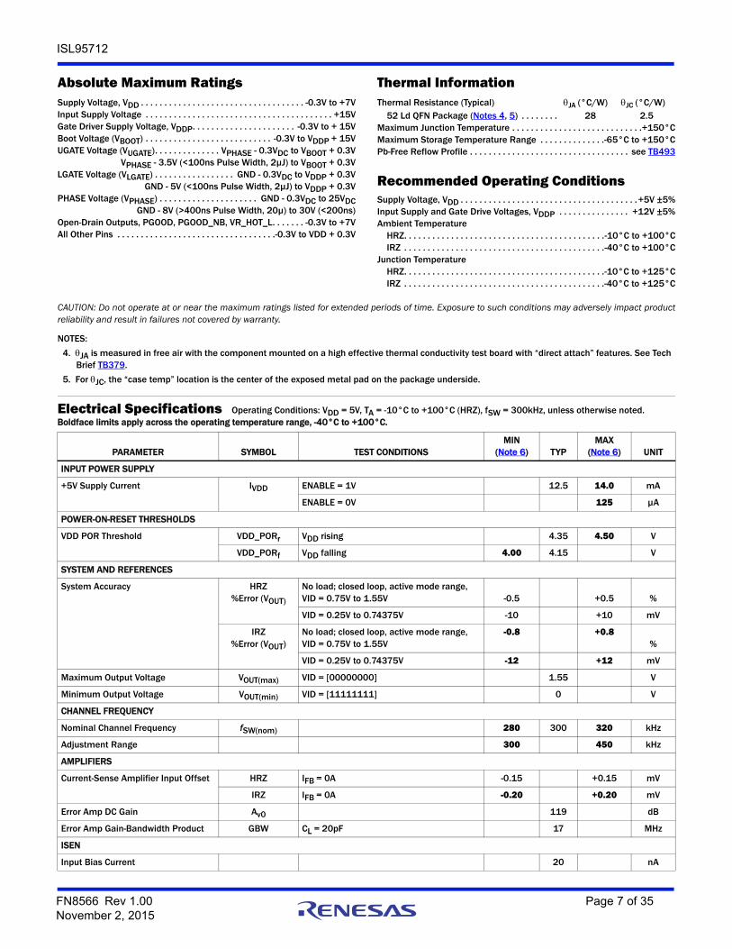
Absolute Maximum Ratings Thermal InformationSupply Voltage, VDD . . . . . . . . . . . . . . . . . . . . . . . . . . . . . . . . . . . -0.3V to +7VInput Supply Voltage . . . . . . . . . . . . . . . . . . . . . . . . . . . . . . . . . . . . . . . . +15VGate Driver Supply Voltage, VDDP. . . . . . . . . . . . . . . . . . . . . . -0.3V to + 15VBoot Voltage (VBOOT) . . . . . . . . . . . . . . . . . . . . . . . . . . . -0.3V to VDDP + 15VUGATE Voltage (VUGATE). . . . . . . . . . . . . . VPHASE - 0.3VDC to VBOOT + 0.3V
VPHASE - 3.5V (<100ns Pulse Width, 2µJ) to VBOOT + 0.3VLGATE Voltage (VLGATE) . . . . . . . . . . . . . . . . . GND - 0.3VDC to VDDP + 0.3V
GND - 5V (<100ns Pulse Width, 2µJ) to VDDP + 0.3VPHASE Voltage (VPHASE) . . . . . . . . . . . . . . . . . . . . . GND - 0.3VDC to 25VDC
GND - 8V (>400ns Pulse Width, 20µ) to 30V (<200ns)Open-Drain Outputs, PGOOD, PGOOD_NB, VR_HOT_L. . . . . . . -0.3V to +7VAll Other Pins . . . . . . . . . . . . . . . . . . . . . . . . . . . . . . . . . .-0.3V to VDD + 0.3V
Thermal Resistance (Typical) JA (°C/W) JC (°C/W)52 Ld QFN Package (Notes 4, 5) . . . . . . . . 28 2.5
Maximum Junction Temperature . . . . . . . . . . . . . . . . . . . . . . . . . . . .+150°CMaximum Storage Temperature Range . . . . . . . . . . . . . .-65°C to +150°CPb-Free Reflow Profile . . . . . . . . . . . . . . . . . . . . . . . . . . . . . . . . . . see TB493
Recommended Operating ConditionsSupply Voltage, VDD . . . . . . . . . . . . . . . . . . . . . . . . . . . . . . . . . . . . . .+5V ±5%Input Supply and Gate Drive Voltages, VDDP . . . . . . . . . . . . . . . +12V ±5%Ambient Temperature
HRZ. . . . . . . . . . . . . . . . . . . . . . . . . . . . . . . . . . . . . . . . . . .-10°C to +100°CIRZ . . . . . . . . . . . . . . . . . . . . . . . . . . . . . . . . . . . . . . . . . . .-40°C to +100°C
Junction TemperatureHRZ. . . . . . . . . . . . . . . . . . . . . . . . . . . . . . . . . . . . . . . . . . .-10°C to +125°CIRZ . . . . . . . . . . . . . . . . . . . . . . . . . . . . . . . . . . . . . . . . . . .-40°C to +125°C
CAUTION: Do not operate at or near the maximum ratings listed for extended periods of time. Exposure to such conditions may adversely impact productreliability and result in failures not covered by warranty.
NOTES:
4. JA is measured in free air with the component mounted on a high effective thermal conductivity test board with “direct attach” features. See Tech Brief TB379.
5. For JC, the “case temp” location is the center of the exposed metal pad on the package underside.
Electrical Specifications Operating Conditions: VDD = 5V, TA = -10°C to +100°C (HRZ), fSW = 300kHz, unless otherwise noted.Boldface limits apply across the operating temperature range, -40°C to +100°C.
PARAMETER SYMBOL TEST CONDITIONSMIN
(Note 6) TYPMAX
(Note 6) UNIT
INPUT POWER SUPPLY
+5V Supply Current IVDD ENABLE = 1V 12.5 14.0 mA
ENABLE = 0V 125 µA
POWER-ON-RESET THRESHOLDS
VDD POR Threshold VDD_PORr VDD rising 4.35 4.50 V
VDD_PORf VDD falling 4.00 4.15 V
SYSTEM AND REFERENCES
System Accuracy HRZ%Error (VOUT)
No load; closed loop, active mode range, VID = 0.75V to 1.55V -0.5 +0.5 %
VID = 0.25V to 0.74375V -10 +10 mV
IRZ%Error (VOUT)
No load; closed loop, active mode range, VID = 0.75V to 1.55V
-0.8 +0.8%
VID = 0.25V to 0.74375V -12 +12 mV
Maximum Output Voltage VOUT(max) VID = [00000000] 1.55 V
Minimum Output Voltage VOUT(min) VID = [11111111] 0 V
CHANNEL FREQUENCY
Nominal Channel Frequency fSW(nom) 280 300 320 kHz
Adjustment Range 300 450 kHz
AMPLIFIERS
Current-Sense Amplifier Input Offset HRZ IFB = 0A -0.15 +0.15 mV
IRZ IFB = 0A -0.20 +0.20 mV
Error Amp DC Gain Av0 119 dB
Error Amp Gain-Bandwidth Product GBW CL = 20pF 17 MHz
ISEN
Input Bias Current 20 nA
FN8566 Rev 1.00 Page 7 of 35November 2, 2015
ISL95712
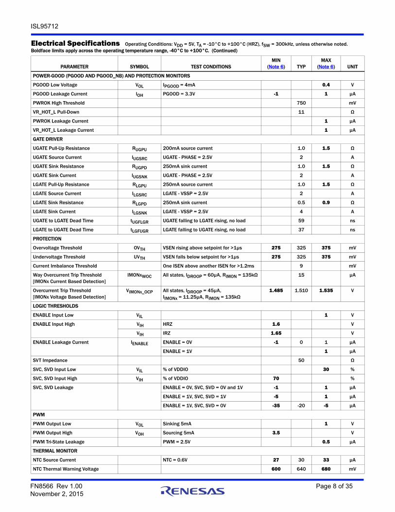
POWER-GOOD (PGOOD AND PGOOD_NB) AND PROTECTION MONITORS
PGOOD Low Voltage VOL IPGOOD = 4mA 0.4 V
PGOOD Leakage Current IOH PGOOD = 3.3V -1 1 µA
PWROK High Threshold 750 mV
VR_HOT_L Pull-Down 11 Ω
PWROK Leakage Current 1 µA
VR_HOT_L Leakage Current 1 µA
GATE DRIVER
UGATE Pull-Up Resistance RUGPU 200mA source current 1.0 1.5 Ω
UGATE Source Current IUGSRC UGATE - PHASE = 2.5V 2 A
UGATE Sink Resistance RUGPD 250mA sink current 1.0 1.5 Ω
UGATE Sink Current IUGSNK UGATE - PHASE = 2.5V 2 A
LGATE Pull-Up Resistance RLGPU 250mA source current 1.0 1.5 Ω
LGATE Source Current ILGSRC LGATE - VSSP = 2.5V 2 A
LGATE Sink Resistance RLGPD 250mA sink current 0.5 0.9 Ω
LGATE Sink Current ILGSNK LGATE - VSSP = 2.5V 4 A
UGATE to LGATE Dead Time tUGFLGR UGATE falling to LGATE rising, no load 59 ns
LGATE to UGATE Dead Time tLGFUGR LGATE falling to UGATE rising, no load 37 ns
PROTECTION
Overvoltage Threshold OVTH VSEN rising above setpoint for >1µs 275 325 375 mV
Undervoltage Threshold UVTH VSEN falls below setpoint for >1µs 275 325 375 mV
Current Imbalance Threshold One ISEN above another ISEN for >1.2ms 9 mV
Way Overcurrent Trip Threshold[IMONx Current Based Detection]
IMONxWOC All states, IDROOP = 60µA, RIMON = 135kΩ 15 µA
Overcurrent Trip Threshold[IMONx Voltage Based Detection]
VIMONx_OCP All states, IDROOP = 45µA, IIMONx = 11.25µA, RIMON = 135kΩ
1.485 1.510 1.535 V
LOGIC THRESHOLDS
ENABLE Input Low VIL 1 V
ENABLE Input High VIH HRZ 1.6 V
VIH IRZ 1.65 V
ENABLE Leakage Current IENABLE ENABLE = 0V -1 0 1 µA
ENABLE = 1V 1 µA
SVT Impedance 50 Ω
SVC, SVD Input Low VIL % of VDDIO 30 %
SVC, SVD Input High VIH % of VDDIO 70 %
SVC, SVD Leakage ENABLE = 0V, SVC, SVD = 0V and 1V -1 1 µA
ENABLE = 1V, SVC, SVD = 1V -5 1 µA
ENABLE = 1V, SVC, SVD = 0V -35 -20 -5 µA
PWM
PWM Output Low V0L Sinking 5mA 1 V
PWM Output High V0H Sourcing 5mA 3.5 V
PWM Tri-State Leakage PWM = 2.5V 0.5 µA
THERMAL MONITOR
NTC Source Current NTC = 0.6V 27 30 33 µA
NTC Thermal Warning Voltage 600 640 680 mV
Electrical Specifications Operating Conditions: VDD = 5V, TA = -10°C to +100°C (HRZ), fSW = 300kHz, unless otherwise noted.Boldface limits apply across the operating temperature range, -40°C to +100°C. (Continued)
PARAMETER SYMBOL TEST CONDITIONSMIN
(Note 6) TYPMAX
(Note 6) UNIT
FN8566 Rev 1.00 Page 8 of 35November 2, 2015
ISL95712
Gate Driver Timing Diagram
NTC Thermal Warning Voltage Hysteresis
20 mV
NTC Thermal Shutdown Voltage 530 580 630 mV
SLEW RATE
VID-on-the-Fly Slew Rate Maximum Programmed 16 20 24 mV/µs
Minimum Programmed 8 10 12 mV/µs
NOTE:6. Compliance to datasheet limits is assured by one or more methods: production test, characterization and/or design.
Electrical Specifications Operating Conditions: VDD = 5V, TA = -10°C to +100°C (HRZ), fSW = 300kHz, unless otherwise noted.Boldface limits apply across the operating temperature range, -40°C to +100°C. (Continued)
PARAMETER SYMBOL TEST CONDITIONSMIN
(Note 6) TYPMAX
(Note 6) UNIT
PWM
UGATE
LGATE 1V
1V
tUGFLGR
tRL
tFUtRU
tFL
tLGFUGR
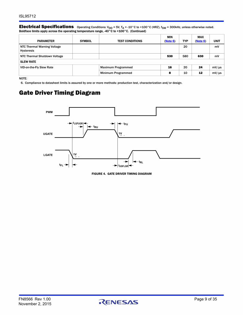
FIGURE 4. GATE DRIVER TIMING DIAGRAM
FN8566 Rev 1.00 Page 9 of 35November 2, 2015
ISL95712
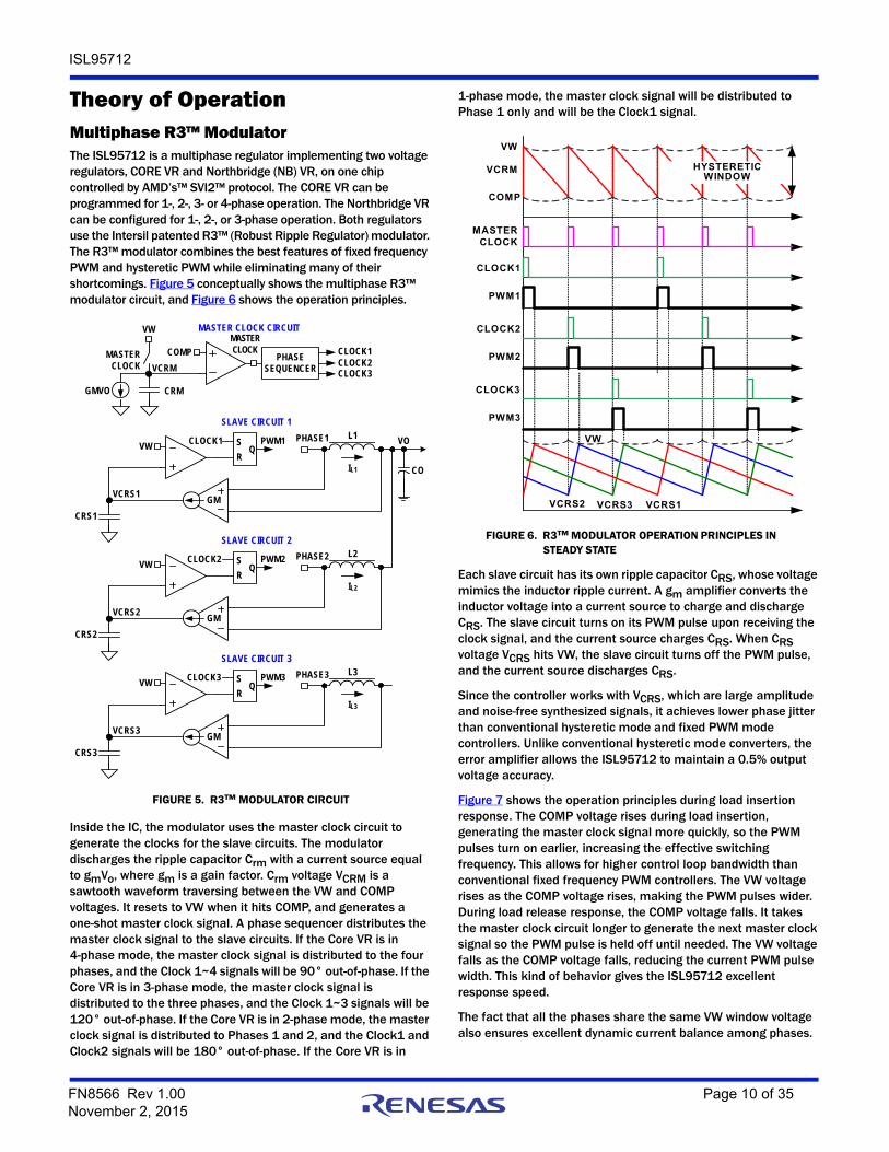
Theory of OperationMultiphase R3™ ModulatorThe ISL95712 is a multiphase regulator implementing two voltage regulators, CORE VR and Northbridge (NB) VR, on one chip controlled by AMD’s™ SVI2™ protocol. The CORE VR can be programmed for 1-, 2-, 3- or 4-phase operation. The Northbridge VR can be configured for 1-, 2-, or 3-phase operation. Both regulators use the Intersil patented R3™ (Robust Ripple Regulator) modulator. The R3™ modulator combines the best features of fixed frequency PWM and hysteretic PWM while eliminating many of their shortcomings. Figure 5 conceptually shows the multiphase R3™ modulator circuit, and Figure 6 shows the operation principles.
Inside the IC, the modulator uses the master clock circuit to generate the clocks for the slave circuits. The modulator discharges the ripple capacitor Crm with a current source equal to gmVo, where gm is a gain factor. Crm voltage VCRM is a sawtooth waveform traversing between the VW and COMP voltages. It resets to VW when it hits COMP, and generates a one-shot master clock signal. A phase sequencer distributes the master clock signal to the slave circuits. If the Core VR is in 4-phase mode, the master clock signal is distributed to the four phases, and the Clock 1~4 signals will be 90° out-of-phase. If the Core VR is in 3-phase mode, the master clock signal is distributed to the three phases, and the Clock 1~3 signals will be 120° out-of-phase. If the Core VR is in 2-phase mode, the master clock signal is distributed to Phases 1 and 2, and the Clock1 and Clock2 signals will be 180° out-of-phase. If the Core VR is in
1-phase mode, the master clock signal will be distributed to Phase 1 only and will be the Clock1 signal.
Each slave circuit has its own ripple capacitor CRS, whose voltage mimics the inductor ripple current. A gm amplifier converts the inductor voltage into a current source to charge and discharge CRS. The slave circuit turns on its PWM pulse upon receiving the clock signal, and the current source charges CRS. When CRS voltage VCRS hits VW, the slave circuit turns off the PWM pulse, and the current source discharges CRS.
Since the controller works with VCRS, which are large amplitude and noise-free synthesized signals, it achieves lower phase jitter than conventional hysteretic mode and fixed PWM mode controllers. Unlike conventional hysteretic mode converters, the error amplifier allows the ISL95712 to maintain a 0.5% output voltage accuracy.
Figure 7 shows the operation principles during load insertion response. The COMP voltage rises during load insertion, generating the master clock signal more quickly, so the PWM pulses turn on earlier, increasing the effective switching frequency. This allows for higher control loop bandwidth than conventional fixed frequency PWM controllers. The VW voltage rises as the COMP voltage rises, making the PWM pulses wider. During load release response, the COMP voltage falls. It takes the master clock circuit longer to generate the next master clock signal so the PWM pulse is held off until needed. The VW voltage falls as the COMP voltage falls, reducing the current PWM pulse width. This kind of behavior gives the ISL95712 excellent response speed.
The fact that all the phases share the same VW window voltage also ensures excellent dynamic current balance among phases.
FIGURE 5. R3™ MODULATOR CIRCUIT
CRMGMVO
MASTER CLOCK
VW
COMP
MASTER CLOCK
PHASE SEQUENCER
CLOCK1CLOCK2
RIL1
GM
CLOCK1 PHASE1
CRS1
VW SQ
PWM1 L1
RIL2
GM
CLOCK2 PHASE2
CRS2
VW SQ
PWM2 L2
CO
VO
VCRM
VCRS1
VCRS2
MASTER CLOCK CIRCUIT
SLAVE CIRCUIT 1
SLAVE CIRCUIT 2
RIL3
GM
CLOCK3 PHASE3
CRS3
VW SQ
PWM3 L3
VCRS3
SLAVE CIRCUIT 3
CLOCK3
FIGURE 6. R3™ MODULATOR OPERATION PRINCIPLES IN STEADY STATE
COMP
VCRM
MASTERCLOCK
PWM1
VW
CLOCK1
PWM2
CLOCK2
HYSTERETIC WINDOW
PWM3
VCRS3
CLOCK3
VCRS2 VCRS1
VW
FN8566 Rev 1.00 Page 10 of 35November 2, 2015
ISL95712
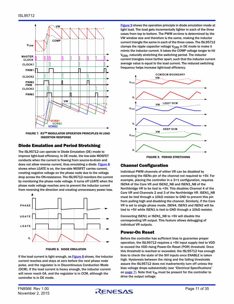
Diode Emulation and Period StretchingThe ISL95712 can operate in Diode Emulation (DE) mode to improve light-load efficiency. In DE mode, the low-side MOSFET conducts when the current is flowing from source-to-drain and does not allow reverse current, thus emulating a diode. Figure 8 shows when LGATE is on, the low-side MOSFET carries current, creating negative voltage on the phase node due to the voltage drop across the ON-resistance. The ISL95712 monitors the current by monitoring the phase node voltage. It turns off LGATE when the phase node voltage reaches zero to prevent the inductor current from reversing the direction and creating unnecessary power loss.
If the load current is light enough, as Figure 8 shows, the inductor current reaches and stays at zero before the next phase node pulse, and the regulator is in Discontinuous Conduction Mode (DCM). If the load current is heavy enough, the inductor current will never reach 0A, and the regulator is in CCM, although the controller is in DE mode.
Figure 9 shows the operation principle in diode emulation mode at light load. The load gets incrementally lighter in each of the three cases from top to bottom. The PWM on-time is determined by the VW window size and therefore is the same, making the inductor current triangle the same in each of the three cases. The ISL95712 clamps the ripple capacitor voltage VCRS in DE mode to make it mimic the inductor current. It takes the COMP voltage longer to hit VCRS, naturally stretching the switching period. The inductor current triangles move farther apart, such that the inductor current average value is equal to the load current. The reduced switching frequency helps increase light-load efficiency.
Channel ConfigurationIndividual PWM channels of either VR can be disabled by connecting the ISENx pin of the channel not required to +5V. For example, placing the controller in a 3+1 configuration, requires ISEN4 of the Core VR and ISEN2_NB and ISEN3_NB of the Northbridge VR to be tied to +5V. This disables Channel 4 of the Core VR and Channels 2 and 3 of the Northbridge VR. ISEN1_NB must be tied through a 10kΩ resistor to GND to prevent this pin from pulling high and disabling the channel. Similarly, if the Core VR is set to single phase mode, ISEN4, ISEN3 and ISEN2 will be tied to +5V while ISEN1 is tied to GND through a 10kΩ resistor.
Connecting ISEN1 or ISEN1_NB to +5V will disable the corresponding VR output. This feature allows debugging of individual VR outputs.
Power-On ResetBefore the controller has sufficient bias to guarantee proper operation, the ISL95712 requires a +5V input supply tied to VDD to exceed the VDD rising Power-On Reset (POR) threshold. Once this threshold is reached or exceeded, the ISL95712 has enough bias to check the state of the SVI inputs once ENABLE is taken high. Hysteresis between the rising and the falling thresholds assure the ISL95712 does not inadvertently turn off unless the bias voltage drops substantially (see “Electrical Specifications” on page 7). Note that VIN must be present for the controller to drive the output voltage.
FIGURE 7. R3™ MODULATOR OPERATION PRINCIPLES IN LOAD INSERTION RESPONSE
COMP
VCRM
MASTERCLOCK
PWM1
VCRS1
VW
CLOCK1
PWM2
VCRS2
CLOCK2
PWM3
CLOCK3
VCRS3
VW
PWM
U G A TE
P H A S E
IL
LG A TE
FIGURE 8. DIODE EMULATION
IL
IL
VCRS
IL
VCRS
VCRS
VWCCM/DCM BOUNDARY
LIGHT DCM
DEEP DCM
VW
VW
FIGURE 9. PERIOD STRETCHING
FN8566 Rev 1.00 Page 11 of 35November 2, 2015
ISL95712
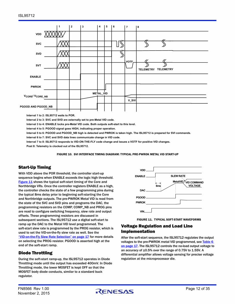
Start-Up TimingWith VDD above the POR threshold, the controller start-up sequence begins when ENABLE exceeds the logic high threshold. Figure 11 shows the typical soft-start timing of the Core and Northbridge VRs. Once the controller registers ENABLE as a high, the controller checks the state of a few programming pins during the typical 8ms delay prior to beginning soft-starting the Core and Northbridge outputs. The pre-PWROK Metal VID is read from the state of the SVC and SVD pins and programs the DAC, the programming resistors on the COMP, COMP_NB and PROG pins are read to configure switching frequency, slew rate and output offsets. These programming resistors are discussed in subsequent sections. The ISL95712 use a digital soft-start to ramp up the DAC to the Metal VID level programmed. The soft-start slew rate is programmed by the PROG resistor, which is used to set the VID-on-the-fly slew rate as well. See the “VID-on-the-Fly Slew Rate Selection” on page 17 for more details on selecting the PROG resistor. PGOOD is asserted high at the end of the soft-start ramp.
Diode ThrottlingDuring the soft-start ramp-up, the ISL95712 operates in Diode Throttling mode until the output has exceeded 400mV. In Diode Throttling mode, the lower MOSFET is kept OFF so that the MOSFET body diode conducts, similar to a standard buck regulator.
Voltage Regulation and Load Line ImplementationAfter the soft-start sequence, the ISL95712 regulates the output voltages to the pre-PWROK metal VID programmed, see Table 6 on page 17. The ISL95712 controls the no-load output voltage to an accuracy of ±0.5% over the range of 0.75V to 1.55V. A differential amplifier allows voltage sensing for precise voltage regulation at the microprocessor die.
VDD
SVC
SVD
ENABLE
PWROK
VCORE/ VCORE_NB
1 7 8
FIGURE 10. SVI INTERFACE TIMING DIAGRAM: TYPICAL PRE-PWROK METAL VID START-UP
PGOOD AND PGOOD_NB
3 42 5 6
METAL_VID
V_SVI
Interval 1 to 2: ISL95712 waits to POR.
Interval 2 to 3: SVC and SVD are externally set to pre-Metal VID code.
Interval 3 to 4: ENABLE locks pre-Metal VID code. Both outputs soft-start to this level.
Interval 4 to 5: PGOOD signal goes HIGH, indicating proper operation.
Interval 6 to 7: SVC and SVD data lines communicate change in VID code.
Interval 7 to 8: ISL95712 responds to VID-ON-THE-FLY code change and issues a VOTF for positive VID changes.
Interval 5 to 6: PGOOD and PGOOD_NB high is detected and PWROK is taken high. The ISL95712 is prepared for SVI commands.
SVT
TELEMETRY TELEMETRY
VOTF
Post 8: Telemetry is clocked out of the ISL95712.
VDD
ENABLE
DAC
8ms
MetalVID
SLEW RATE
VID COMMAND VOLTAGE
PGOOD
PWROK
VIN
FIGURE 11. TYPICAL SOFT-START WAVEFORMS
FN8566 Rev 1.00 Page 12 of 35November 2, 2015
ISL95712
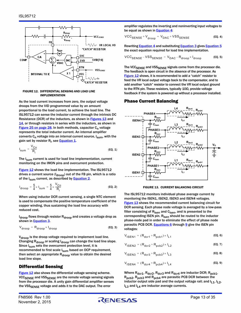
As the load current increases from zero, the output voltage droops from the VID programmed value by an amount proportional to the load current, to achieve the load line. The ISL95712 can sense the inductor current through the intrinsic DC Resistance (DCR) of the inductors, as shown in Figures 13 and 14, or through resistors in series with the inductors, as shown in Figure 25 on page 28. In both methods, capacitor Cn voltage represents the total inductor current. An internal amplifier converts Cn voltage into an internal current source, Isum, with the gain set by resistor Ri, see Equation 1.
The Isum current is used for load line implementation, current monitoring on the IMON pins and overcurrent protection.
Figure 12 shows the load line implementation. The ISL95712 drives a current source (Idroop) out of the FB pin, which is a ratio of the Isum current, as described by Equation 2.
When using inductor DCR current sensing, a single NTC element is used to compensate the positive temperature coefficient of the copper winding, thus sustaining the load line accuracy with reduced cost.
Idroop flows through resistor Rdroop and creates a voltage drop as shown in Equation 3.
Vdroop is the droop voltage required to implement load line. Changing Rdroop or scaling Idroop can change the load line slope. Since Isum sets the overcurrent protection level, it is recommended to first scale Isum based on OCP requirement, then select an appropriate Rdroop value to obtain the desired load line slope.
Differential SensingFigure 12 also shows the differential voltage sensing scheme. VCCSENSE and VSSSENSE are the remote voltage sensing signals from the processor die. A unity gain differential amplifier senses the VSSSENSE voltage and adds it to the DAC output. The error
amplifier regulates the inverting and noninverting input voltages to be equal as shown in Equation 4:
Rewriting Equation 4 and substituting Equation 3 gives Equation 5 the exact equation required for load line implementation.
The VCCSENSE and VSSSENSE signals come from the processor die. The feedback is open circuit in the absence of the processor. As Figure 12 shows, it is recommended to add a “catch” resistor to feed the VR local output voltage back to the compensator, and to add another “catch” resistor to connect the VR local output ground to the RTN pin. These resistors, typically 10Ω, provide voltage feedback if the system is powered up without a processor installed.
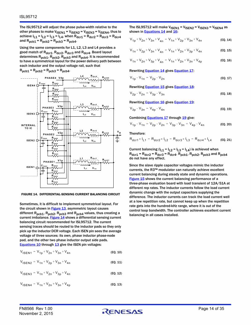
Phase Current Balancing
The ISL95712 monitors individual phase average current by monitoring the ISEN1, ISEN2, ISEN3 and ISEN4 voltages. Figure 13 shows the recommended current balancing circuit for DCR sensing. Each phase node voltage is averaged by a low-pass filter consisting of Risen and Cisen, and is presented to the corresponding ISEN pin. Risen should be routed to the inductor phase-node pad in order to eliminate the effect of phase node parasitic PCB DCR. Equations 6 through 9 give the ISEN pin voltages:
Where Rdcr1, Rdcr2, Rdcr3 and Rdcr4 are inductor DCR; Rpcb1, Rpcb2, Rpcb3 and Rpcb4 are parasitic PCB DCR between the inductor output side pad and the output voltage rail; and IL1, IL2, IL3 and IL4 are inductor average currents.
FIGURE 12. DIFFERENTIAL SENSING AND LOAD LINE IMPLEMENTATION
X 1
E/A
DAC SVID[7:0]
Rdroop
Idroop
VDAC
VdroopFB
COMP
VCCSENSE
VSSSENSE
RTN
VSSINTERNAL TO IC
“CATCH” RESISTOR
“CATCH” RESISTOR
VR LOCAL VO
+
-
+ -
+
+
-
SVC
SVD
Isum
VCnRi-----------= (EQ. 1)
Idroop54--- Isum 5
4---
VCnRi-----------= = (EQ. 2)
Vdroop Rdroop Idroop= (EQ. 3)
VCCSENSE V+droop
VDAC VSSSENSE+= (EQ. 4)
VCCSENSE VSSSENSE– VDAC Rdroop Idroop–= (EQ. 5)
FIGURE 13. CURRENT BALANCING CIRCUIT
VO
ISEN3
L3
Risen
Cisen
ISEN2Risen
Cisen
ISEN1Risen
Cisen
L2
L1
Rdcr3
Rdcr2
Rdcr1
PHASE3
PHASE2
PHASE1
IL3
IL2
IL1
Rpcb3
Rpcb2
Rpcb1
L4 Rdcr4
IL4
Rpcb4
PHASE4Risen
Cisen
ISEN4
VISEN1 Rdcr1 Rpcb1+ IL1= (EQ. 6)
VISEN2 Rdcr2 Rpcb2+ IL2= (EQ. 7)
VISEN3 Rdcr3 Rpcb3+ IL3= (EQ. 8)
VISEN4 Rdcr4 Rpcb4+ IL4= (EQ. 9)
FN8566 Rev 1.00 Page 13 of 35November 2, 2015
ISL95712
The ISL95712 will adjust the phase pulse-width relative to the other phases to make VISEN1 = VISEN2 = VISEN3 = VISEN4, thus to achieve IL1 = IL2 = IL3 = IL4, when Rdcr1 = Rdcr2 = Rdcr3 = Rdcr4 and Rpcb1 = Rpcb2 = Rpcb3 = Rpcb4.
Using the same components for L1, L2, L3 and L4 provides a good match of Rdcr1, Rdcr2, Rdcr3 and Rdcr4. Board layout determines Rpcb1, Rpcb2, Rpcb3 and Rpcb4. It is recommended to have a symmetrical layout for the power delivery path between each inductor and the output voltage rail, such that Rpcb1 = Rpcb2 = Rpcb3 = Rpcb4.
Sometimes, it is difficult to implement symmetrical layout. For the circuit shown in Figure 13, asymmetric layout causes different Rpcb1, Rpcb2, Rpcb3 and Rpcb4 values, thus creating a current imbalance. Figure 14 shows a differential sensing current balancing circuit recommended for ISL95712. The current sensing traces should be routed to the inductor pads so they only pick up the inductor DCR voltage. Each ISEN pin sees the average voltage of three sources: its own, phase inductor phase-node pad, and the other two phase inductor output side pads. Equations 10 through 13 give the ISEN pin voltages:
The ISL95712 will make VISEN1 = VISEN2 = VISEN3 = VISEN4 as shown in Equations 14 and 16:
Rewriting Equation 14 gives Equation 17:
Rewriting Equation 15 gives Equation 18:
Rewriting Equation 16 gives Equation 19:
Combining Equations 17 through 19 give:
Therefore:
Current balancing (IL1 = IL2 = IL3 = IL4) is achieved when Rdcr1 = Rdcr2 = Rdcr3 = Rdcr4. Rpcb1, Rpcb2, Rpcb3 and Rpcb4 do not have any effect.
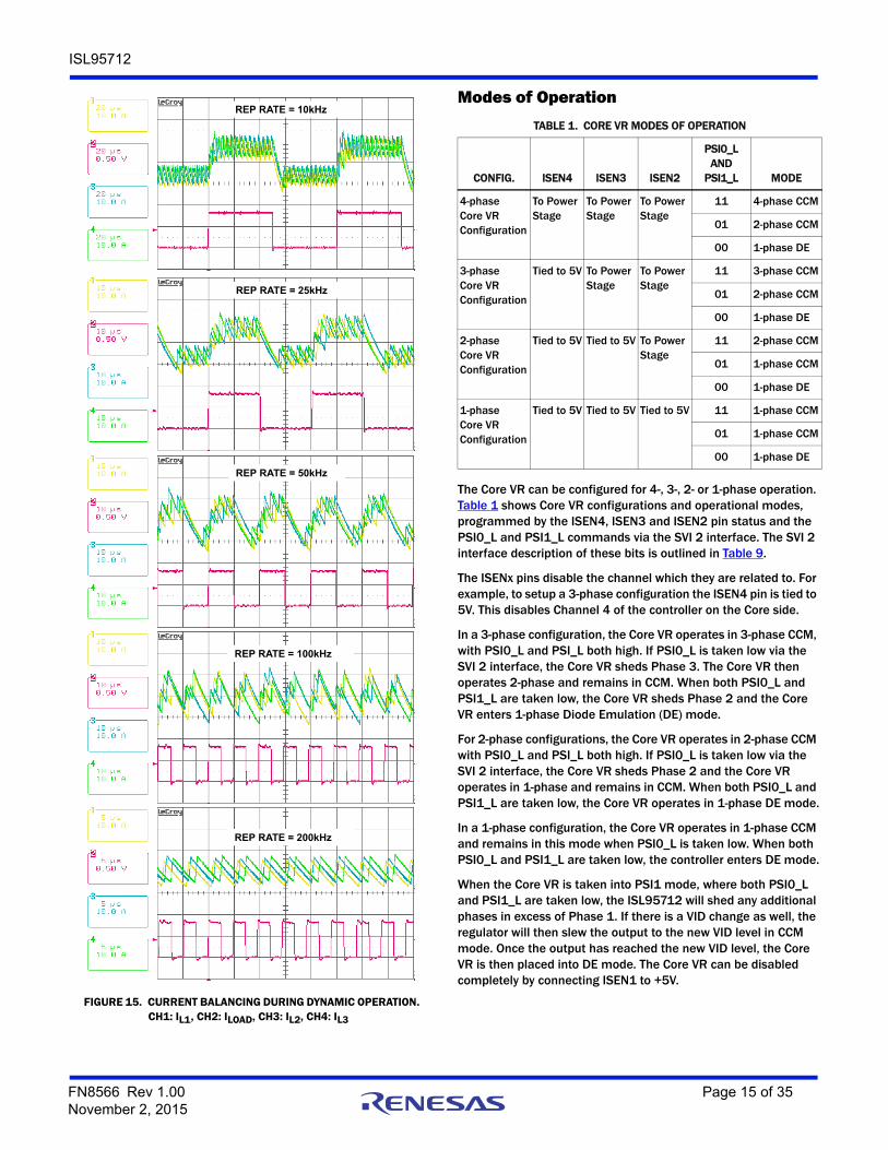
Since the slave ripple capacitor voltages mimic the inductor currents, the R3™ modulator can naturally achieve excellent current balancing during steady state and dynamic operations. Figure 15 shows the current balancing performance of a three-phase evaluation board with load transient of 12A/51A at different rep rates. The inductor currents follow the load current dynamic change with the output capacitors supplying the difference. The inductor currents can track the load current well at a low repetition rate, but cannot keep up when the repetition rate gets into the hundred-kHz range, where it is out of the control loop bandwidth. The controller achieves excellent current balancing in all cases installed.
FIGURE 14. DIFFERENTIAL-SENSING CURRENT BALANCING CIRCUIT
IN TERN AL TO IC
Vo
ISEN 3
L3
R isenC isen
ISE N 2R isenC isen
ISEN 1R isenC isen
L2
L1
R dcr3
R dcr2
R dcr1
PHA SE 3
PHA SE2
PHA SE 1
IL3
IL2
IL1
R pcb3
R pcb2
R pcb1
R isen
R isen
R isen
R isen
R isen
R isen
V3p
V 3n
V2p
V 2n
V1p
V 1n
L4 R dcr4
IL4
R pcb4
V 4n
V 4pPHASE4
R isenC isen
R isen
R isen
R isen
R isen
R isen
R isen
IS EN 4
VISEN1 V1p V2n V3n V4n+ + += (EQ. 10)
VISEN2 V1n V2p V3n V4n+ + += (EQ. 11)
VISEN3 V1n V2n V3p V4n+ + += (EQ. 12)
VISEN4 V1n V2n V3n V4p+ + += (EQ. 13)
V1p V2n V3n V+4n
+ + V1n V2p V3n V4n+ + += (EQ. 14)
V1n V2p V3n V+4n
+ + V1n V2n V3p V4n+ + += (EQ. 15)
V1n V2n V3p V+4n
+ + V1n V2n V3n V4p+ + += (EQ. 16)
V1p V1n– V2p V2n–= (EQ. 17)
V2p V2n– V3p V3n–= (EQ. 18)
V3p V3n– V4p V4n–= (EQ. 19)
V1p V1n– V2p V2n– V3p V3n– V4p V4n–= = = (EQ. 20)
Rdcr1 IL1 Rdcr2 IL2 Rdcr3 IL3 Rdcr4 IL4= = = (EQ. 21)
FN8566 Rev 1.00 Page 14 of 35November 2, 2015
ISL95712
Modes of Operation
The Core VR can be configured for 4-, 3-, 2- or 1-phase operation. Table 1 shows Core VR configurations and operational modes, programmed by the ISEN4, ISEN3 and ISEN2 pin status and the PSI0_L and PSI1_L commands via the SVI 2 interface. The SVI 2 interface description of these bits is outlined in Table 9.
The ISENx pins disable the channel which they are related to. For example, to setup a 3-phase configuration the ISEN4 pin is tied to 5V. This disables Channel 4 of the controller on the Core side.
In a 3-phase configuration, the Core VR operates in 3-phase CCM, with PSI0_L and PSI_L both high. If PSI0_L is taken low via the SVI 2 interface, the Core VR sheds Phase 3. The Core VR then operates 2-phase and remains in CCM. When both PSI0_L and PSI1_L are taken low, the Core VR sheds Phase 2 and the Core VR enters 1-phase Diode Emulation (DE) mode.
For 2-phase configurations, the Core VR operates in 2-phase CCM with PSI0_L and PSI_L both high. If PSI0_L is taken low via the SVI 2 interface, the Core VR sheds Phase 2 and the Core VR operates in 1-phase and remains in CCM. When both PSI0_L and PSI1_L are taken low, the Core VR operates in 1-phase DE mode.
In a 1-phase configuration, the Core VR operates in 1-phase CCM and remains in this mode when PSI0_L is taken low. When both PSI0_L and PSI1_L are taken low, the controller enters DE mode.
When the Core VR is taken into PSI1 mode, where both PSI0_L and PSI1_L are taken low, the ISL95712 will shed any additional phases in excess of Phase 1. If there is a VID change as well, the regulator will then slew the output to the new VID level in CCM mode. Once the output has reached the new VID level, the Core VR is then placed into DE mode. The Core VR can be disabled completely by connecting ISEN1 to +5V.
FIGURE 15. CURRENT BALANCING DURING DYNAMIC OPERATION. CH1: IL1, CH2: ILOAD, CH3: IL2, CH4: IL3
REP RATE = 10kHz
REP RATE = 25kHz
REP RATE = 50kHz
REP RATE = 100kHz
REP RATE = 200kHz
TABLE 1. CORE VR MODES OF OPERATION
CONFIG. ISEN4 ISEN3 ISEN2
PSI0_L AND
PSI1_L MODE
4-phase Core VR Configuration
To Power Stage
To Power Stage
To Power Stage
11 4-phase CCM
01 2-phase CCM
00 1-phase DE
3-phase Core VR Configuration
Tied to 5V To Power Stage
To Power Stage
11 3-phase CCM
01 2-phase CCM
00 1-phase DE
2-phaseCore VR Configuration
Tied to 5V Tied to 5V To Power Stage
11 2-phase CCM
01 1-phase CCM
00 1-phase DE
1-phaseCore VR Configuration
Tied to 5V Tied to 5V Tied to 5V 11 1-phase CCM
01 1-phase CCM
00 1-phase DE
FN8566 Rev 1.00 Page 15 of 35November 2, 2015
ISL95712
The ISL95712 Northbridge VR can be configured for 3-, 2-, or 1-phase operation. Table 2 shows the Northbridge VR configurations and operational modes, which are programmed by the ISEN3_NB and ISEN2_NB pin status and the PSI0_L and PSI1_L bits of the SVI 2 command.
In a 1-phase configuration, the ISEN2_NB pin is tied to +5V. The Northbridge VR operates in 1-phase CCM when both PSI0_L and PSI1_L are high and continues in this mode when PSI0_L is taken low. The controller enters 1-phase DE mode when both PSI0_L and PSI1_L are low.
When the Northbridge VR is taken into PSI1 mode, where both PSI0_L and PSI1_L are taken low, the ISL95712 will shed any additional phases in excess of Phase 1. If there is a VID change as well, the regulator will then slew the output to the new VID level in CCM mode. Once the output has reached the new VID level, the Northbridge VR is then placed into DE mode.
The Northbridge VR can be disabled completely by tying ISEN1_NB to 5V.
Dynamic OperationCore and Northbridge VRs behave the same during dynamic operation. The controller responds to VID-on-the-fly changes by slewing to the new voltage at the slew rate programmed, see Table 4. During negative VID transitions, the output voltage decays to the lower VID value at the slew rate determined by the load.
The R3™ modulator intrinsically has voltage feed-forward. The output voltage is insensitive to a fast slew rate input voltage change.
Adaptive Body Diode Conduction Time ReductionIn DCM, the controller turns off the low-side MOSFET when the inductor current approaches zero. During on-time of the low-side MOSFET, phase voltage is negative and the amount is the MOSFET rDS(ON) voltage drop, which is proportional to the inductor current. A phase comparator inside the controller monitors the phase voltage during on-time of the low-side MOSFET and compares it with a threshold to determine the zero crossing point of the inductor current. If the inductor current has
not reached zero when the low-side MOSFET turns off, it will flow through the low-side MOSFET body diode, causing the phase node to have a larger voltage drop until it decays to zero. If the inductor current has crossed zero and reversed the direction when the low-side MOSFET turns off, it will flow through the high-side MOSFET body diode, causing the phase node to have a spike until it decays to zero. The controller continues monitoring the phase voltage after turning off the low-side MOSFET. To minimize the body diode-related loss, the controller also adjusts the phase comparator threshold voltage accordingly in iterative steps such that the low-side MOSFET body diode conducts for approximately 40ns.
Resistor Configuration OptionsThe ISL95712 uses the COMP, COMP_NB and PROG pins to configure some functionality within the IC. Resistors from these pins to GND are read during the first portion of the soft-start sequence. The following sections outline how to select the resistor values for each of these pins to correctly program the output voltage offset of each output, VID-on-the-fly slew rate and switching frequency used for both VRs.
VR Offset ProgrammingA positive or negative offset is programmed for the Core VR using a resistor to ground from the COMP pin and the Northbridge in a similar manner from the COMP_NB pin. Table 3 provides the resistor value to select the desired output voltage offset. The 1% tolerance resistor value shown in Table 3 must be used to program the corresponding Core or NB output voltage offset. The MIN and MAX tolerance values provide margin to insure the 1% tolerance resistor will be read correctly.
TABLE 2. NORTHBRIDGE VR MODES OF OPERATION
CONFIG. ISEN3_NB ISEN2_NBPSI0_L AND
PSI1_L MODE
3-phase NB VR Configuration
To Power Stage
To Power Stage
11 2-phase CCM
01 1-phase CCM
00 1-phase DE
2-phaseNB VR Configuration
Tied to 5V To Power Stage
11 2-phase CCM
01 1-phase CCM
00 1-phase DE
1-phase NB VR Configuration
Tied to 5V Tied to 5V 11 1-phase CCM
01 1-phase CCM
00 1-phase DE
TABLE 3. COMP AND COMP_NB OUTPUT VOLTAGE OFFSET SELECTION
RESISTOR VALUE [kΩ]COMP
VCORE OFFSET [mV]
COMP_NBOFFSET
[mV]MIN
TOLERANCE1% TOLERANCE
VALUEMAX
TOLERANCE
3.96 4.02 4.07 -43.75 18.75
7.76 7.87 7.98 -37.5 31.25
11.33 11.5 11.67 -31.25 43.76
16.65 16.9 17.15 -25 50
19.3 19.6 19.89 -18.75 37.5
24.53 24.9 25.27 -12.5 25
33.49 34.0 34.51 -6.25 12.5
40.58 41.2 41.81 6.25 0
51.52 52.3 53.08 18.75 18.75
72.10 73.2 74.29 31.25 31.25
93.87 95.3 96.72 43.76 43.76
119.19 121 112.81 50 50
151.69 154 156.31 37.5 37.5
179.27 182 184.73 25 25
206.85 210 213.15 12.5 12.5
OPEN 0 0
FN8566 Rev 1.00 Page 16 of 35November 2, 2015
ISL95712
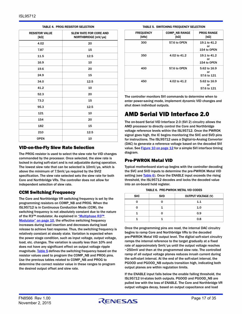
VID-on-the-Fly Slew Rate SelectionThe PROG resistor is used to select the slew rate for VID changes commanded by the processor. Once selected, the slew rate is locked in during soft-start and is not adjustable during operation. The lowest slew rate that can be selected is 10mV/µs, which is above the minimum of 7.5mV/µs required by the SVI2 specification. The slew rate selected sets the slew rate for both Core and Northbridge VRs. The controller does not allow for independent selection of slew rate.
CCM Switching FrequencyThe Core and Northbridge VR switching frequency is set by the programming resistors on COMP_NB and PROG. When the ISL95712 is in Continuous Conduction Mode (CCM), the switching frequency is not absolutely constant due to the nature of the R3™ modulator. As explained in “Multiphase R3™ Modulator” on page 10, the effective switching frequency increases during load insertion and decreases during load release to achieve fast response. Thus, the switching frequency is relatively constant at steady state. Variation is expected when the power stage condition, such as input voltage, output voltage, load, etc. changes. The variation is usually less than 10% and does not have any significant effect on output voltage ripple magnitude. Table 5 defines the switching frequency based on the resistor values used to program the COMP_NB and PROG pins. Use the previous tables related to COMP_NB and PROG to determine the correct resistor value in these ranges to program the desired output offset and slew rate.
The controller monitors SVI commands to determine when to enter power-saving mode, implement dynamic VID changes and shut down individual outputs.
AMD Serial VID Interface 2.0The on-board Serial VID Interface 2.0 (SVI 2) circuitry allows the AMD processor to directly control the Core and Northbridge voltage reference levels within the ISL95712. Once the PWROK signal goes high, the IC begins monitoring the SVC and SVD pins for instructions. The ISL95712 uses a Digital-to-Analog Converter (DAC) to generate a reference voltage based on the decoded SVI value. See Figure 10 on page 12 for a simple SVI interface timing diagram.
Pre-PWROK Metal VIDTypical motherboard start-up begins with the controller decoding the SVC and SVD inputs to determine the pre-PWROK Metal VID setting (see Table 6). Once the ENABLE input exceeds the rising threshold, the ISL95712 decodes and locks the decoded value into an on-board hold register.
Once the programming pins are read, the internal DAC circuitry begins to ramp Core and Northbridge VRs to the decoded pre-PWROK Metal VID output level. The digital soft-start circuitry ramps the internal reference to the target gradually at a fixed rate of approximately 5mV/µs until the output voltage reaches ~250mV and then at the programmed slew rate. The controlled ramp of all output voltage planes reduces inrush current during the soft-start interval. At the end of the soft-start interval, the PGOOD and PGOOD_NB outputs transition high, indicating both output planes are within regulation limits.
If the ENABLE input falls below the enable falling threshold, the ISL95712 tri-states both outputs. PGOOD and PGOOD_NB are pulled low with the loss of ENABLE. The Core and Northbridge VR output voltages decay, based on output capacitance and load
TABLE 4. PROG RESISTOR SELECTION
RESISTOR VALUE[kΩ]
SLEW RATE FOR CORE AND NORTHBRIDGE [mV/µs]
4.02 20
7.87 15
11.5 12.5
16.9 10
19.6 20
24.9 15
34.0 12.5
41.2 10
52.3 20
73.2 15
95.3 12.5
121 10
154 20
182 15
210 12.5
OPEN 10
TABLE 5. SWITCHING FREQUENCY SELECTION
FREQUENCY[kHz]
COMP_NB RANGE[kΩ]
PROG RANGE[kΩ]
300 57.6 to OPEN 19.1 to 41.2or
154 to OPEN
350 4.02 to 41.2 19.1 to 41.2or
154 to OPEN
400 57.6 to OPEN 5.62 to 16.9or
57.6 to 121
450 4.02 to 41.2 5.62 to 16.9or
57.6 to 121
TABLE 6. PRE-PWROK METAL VID CODES
SVC SVD OUTPUT VOLTAGE (V)
0 0 1.1
0 1 1.0
1 0 0.9
1 1 0.8
FN8566 Rev 1.00 Page 17 of 35November 2, 2015
ISL95712
leakage resistance. If bias to VDD falls below the POR level, the The ISL95712 responds in the manner previously described. Once VDD and ENABLE rise above their respective rising thresholds, the internal DAC circuitry reacquires a pre-PWROK metal VID code, and the controller soft-starts.
SVI Interface ActiveOnce the Core and Northbridge VRs have successfully soft-started and PGOOD and PGOOD_NB signals transition high, PWROK can be asserted externally to the ISL95712. Once PWROK is asserted to the IC, SVI instructions can begin as the controller actively monitors the SVI interface. Details of the SVI Bus protocol are provided in the “AMD Serial VID Interface 2.0 (SVI2) Specification”. See AMD publication #48022.
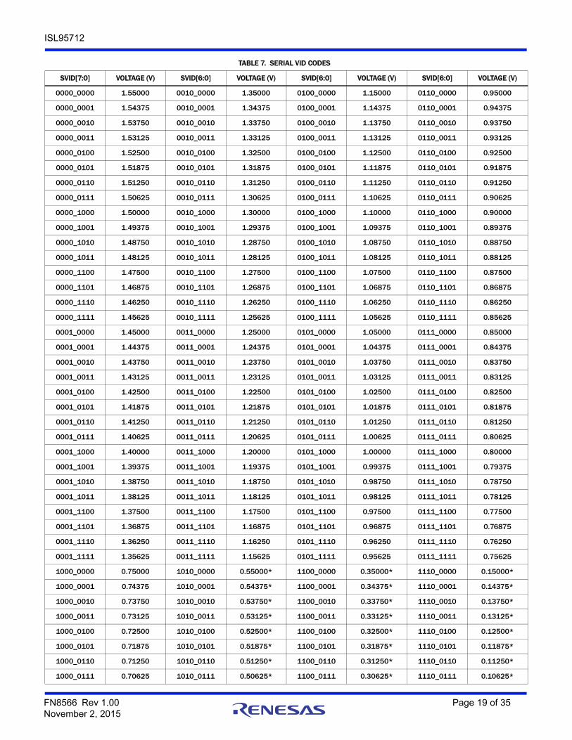
Once a VID change command is received, the ISL95712 decodes the information to determine which VR is affected and the VID target is determined by the byte combinations in Table 7. The internal DAC circuitry steps the output voltage of the VR commanded to the new VID level. During this time, one or more of the VR outputs could be targeted. In the event either VR is commanded to power-off by serial VID commands, the PGOOD signal remains asserted.
If the PWROK input is deasserted, then the controller steps both the Core and the Northbridge VRs back to the stored pre-PWROK metal VID level in the holding register from initial soft-start. No attempt is made to read the SVC and SVD inputs during this time. If PWROK is reasserted, then the ISL95712 SVI interface waits for instructions.
If ENABLE goes low during normal operation, all external MOSFETs are tri-stated and both PGOOD and PGOOD_NB are pulled low. This event clears the pre-PWROK metal VID code and forces the controller to check SVC and SVD upon restart, storing the pre-PWROK metal VID code found on restart.
A POR event on VCC during normal operation shuts down both regulators, and both PGOOD outputs are pulled low. The pre-PWROK metal VID code is not retained. Loss of VIN during operation will typically cause the controller to enter a fault condition on one or both outputs as the output voltage collapses. The controller will shut down both Core and Northbridge VRs and latch off. The pre-PWROK metal VID code is not retained during the process of cycling ENABLE to reset the fault latch and restart the controller.
VID-on-the-Fly TransitionOnce PWROK is high, the ISL95712 detects this flag and begins monitoring the SVC and SVD pins for SVI instructions. The microprocessor follows the protocol outlined in the following sections to send instructions for VID-on-the-fly transitions. The ISL95712 decodes the instruction and acknowledges the new VID code. For VID codes higher than the current VID level, the ISL95712 begins stepping the commanded VR outputs to the new VID target at the fixed slew rate of 10mV/µs. Once the DAC ramps to the new VID code, a VID-on-the-Fly Complete (VOTFC) request is sent on the SVI lines.
When the VID codes are lower than the current VID level, the ISL95712 checks the state of power state bits in the SVI command. If power state bits are not active, the controller begins stepping the regulator output to the new VID target. If the power state bits are active, the controller allows the output voltage to decay and slowly steps the DAC down with the natural decay of the output. This allows the controller to quickly recover and move to a high VID code if commanded. The controller issues a VOTFC request on the SVI lines once the SVI command is decoded and prior to reaching the final output voltage.
VOTFC requests do not take priority over telemetry per the AMD SVI 2 specification.
SVI Data Communication ProtocolThe SVI WIRE protocol is based on the I2C bus concept. Two wires [serial clock (SVC) and serial data (SVD)], carry information between the AMD processor (master) and VR controller (slave) on the bus. The master initiates and terminates SVI transactions and drives the clock, SVC, during a transaction. The AMD processor is always the master and the voltage regulators are the slaves. The slave receives the SVI transactions and acts accordingly. Mobile SVI WIRE protocol timing is based on high-speed mode I2C. See AMD publication #48022 for additional details.
FN8566 Rev 1.00 Page 18 of 35November 2, 2015
ISL95712
TABLE 7. SERIAL VID CODES
SVID[7:0] VOLTAGE (V) SVID[6:0] VOLTAGE (V) SVID[6:0] VOLTAGE (V) SVID[6:0] VOLTAGE (V)
0000_0000 1.55000 0010_0000 1.35000 0100_0000 1.15000 0110_0000 0.95000
0000_0001 1.54375 0010_0001 1.34375 0100_0001 1.14375 0110_0001 0.94375
0000_0010 1.53750 0010_0010 1.33750 0100_0010 1.13750 0110_0010 0.93750
0000_0011 1.53125 0010_0011 1.33125 0100_0011 1.13125 0110_0011 0.93125
0000_0100 1.52500 0010_0100 1.32500 0100_0100 1.12500 0110_0100 0.92500
0000_0101 1.51875 0010_0101 1.31875 0100_0101 1.11875 0110_0101 0.91875
0000_0110 1.51250 0010_0110 1.31250 0100_0110 1.11250 0110_0110 0.91250
0000_0111 1.50625 0010_0111 1.30625 0100_0111 1.10625 0110_0111 0.90625
0000_1000 1.50000 0010_1000 1.30000 0100_1000 1.10000 0110_1000 0.90000
0000_1001 1.49375 0010_1001 1.29375 0100_1001 1.09375 0110_1001 0.89375
0000_1010 1.48750 0010_1010 1.28750 0100_1010 1.08750 0110_1010 0.88750
0000_1011 1.48125 0010_1011 1.28125 0100_1011 1.08125 0110_1011 0.88125
0000_1100 1.47500 0010_1100 1.27500 0100_1100 1.07500 0110_1100 0.87500
0000_1101 1.46875 0010_1101 1.26875 0100_1101 1.06875 0110_1101 0.86875
0000_1110 1.46250 0010_1110 1.26250 0100_1110 1.06250 0110_1110 0.86250
0000_1111 1.45625 0010_1111 1.25625 0100_1111 1.05625 0110_1111 0.85625
0001_0000 1.45000 0011_0000 1.25000 0101_0000 1.05000 0111_0000 0.85000
0001_0001 1.44375 0011_0001 1.24375 0101_0001 1.04375 0111_0001 0.84375
0001_0010 1.43750 0011_0010 1.23750 0101_0010 1.03750 0111_0010 0.83750
0001_0011 1.43125 0011_0011 1.23125 0101_0011 1.03125 0111_0011 0.83125
0001_0100 1.42500 0011_0100 1.22500 0101_0100 1.02500 0111_0100 0.82500
0001_0101 1.41875 0011_0101 1.21875 0101_0101 1.01875 0111_0101 0.81875
0001_0110 1.41250 0011_0110 1.21250 0101_0110 1.01250 0111_0110 0.81250
0001_0111 1.40625 0011_0111 1.20625 0101_0111 1.00625 0111_0111 0.80625
0001_1000 1.40000 0011_1000 1.20000 0101_1000 1.00000 0111_1000 0.80000
0001_1001 1.39375 0011_1001 1.19375 0101_1001 0.99375 0111_1001 0.79375
0001_1010 1.38750 0011_1010 1.18750 0101_1010 0.98750 0111_1010 0.78750
0001_1011 1.38125 0011_1011 1.18125 0101_1011 0.98125 0111_1011 0.78125
0001_1100 1.37500 0011_1100 1.17500 0101_1100 0.97500 0111_1100 0.77500
0001_1101 1.36875 0011_1101 1.16875 0101_1101 0.96875 0111_1101 0.76875
0001_1110 1.36250 0011_1110 1.16250 0101_1110 0.96250 0111_1110 0.76250
0001_1111 1.35625 0011_1111 1.15625 0101_1111 0.95625 0111_1111 0.75625
1000_0000 0.75000 1010_0000 0.55000* 1100_0000 0.35000* 1110_0000 0.15000*
1000_0001 0.74375 1010_0001 0.54375* 1100_0001 0.34375* 1110_0001 0.14375*
1000_0010 0.73750 1010_0010 0.53750* 1100_0010 0.33750* 1110_0010 0.13750*
1000_0011 0.73125 1010_0011 0.53125* 1100_0011 0.33125* 1110_0011 0.13125*
1000_0100 0.72500 1010_0100 0.52500* 1100_0100 0.32500* 1110_0100 0.12500*
1000_0101 0.71875 1010_0101 0.51875* 1100_0101 0.31875* 1110_0101 0.11875*
1000_0110 0.71250 1010_0110 0.51250* 1100_0110 0.31250* 1110_0110 0.11250*
1000_0111 0.70625 1010_0111 0.50625* 1100_0111 0.30625* 1110_0111 0.10625*
FN8566 Rev 1.00 Page 19 of 35November 2, 2015
ISL95712
1000_1000 0.70000 1010_1000 0.50000* 1100_1000 0.30000* 1110_1000 0.10000*
1000_1001 0.69375 1010_1001 0.49375* 1100_1001 0.29375* 1110_1001 0.09375*
1000_1010 0.68750 1010_1010 0.48750* 1100_1010 0.28750* 1110_1010 0.08750*
1000_1011 0.68125 1010_1011 0.48125* 1100_1011 0.28125* 1110_1011 0.08125*
1000_1100 0.67500 1010_1100 0.47500* 1100_1100 0.27500* 1110_1100 0.07500*
1000_1101 0.66875 1010_1101 0.46875* 1100_1101 0.26875* 1110_1101 0.06875*
1000_1110 0.66250 1010_1110 0.46250* 1100_1110 0.26250* 1110_1110 0.06250*
1000_1111 0.65625 1010_1111 0.45625* 1100_1111 0.25625* 1110_1111 0.05625*
1001_0000 0.65000 1011_0000 0.45000* 1101_0000 0.25000* 1111_0000 0.05000*
1001_0001 0.64375 1011_0001 0.44375* 1101_0001 0.24375* 1111_0001 0.04375*
1001_0010 0.63750 1011_0010 0.43750* 1101_0010 0.23750* 1111_0010 0.03750*
1001_0011 0.63125 1011_0011 0.43125* 1101_0011 0.23125* 1111_0011 0.03125*
1001_0100 0.62500 1011_0100 0.42500* 1101_0100 0.22500* 1111_0100 0.02500*
1001_0101 0.61875 1011_0101 0.41875* 1101_0101 0.21875* 1111_0101 0.01875*
1001_0110 0.61250 1011_0110 0.41250* 1101_0110 0.21250* 1111_0110 0.01250*
1001_0111 0.60625 1011_0111 0.40625* 1101_0111* 0.20625* 1111_0111 0.00625*
1001_1000 0.60000* 1011_1000 0.40000* 1101_1000 0.20000* 1111_1000 OFF*
1001_1001 0.59375* 1011_1001 0.39375* 1101_1001 0.19375* 1111_1001 OFF*
1001_1010 0.58750* 1011_1010 0.38750* 1101_1010 0.18750* 1111_1010 OFF*
1001_1011 0.58125* 1011_1011 0.38125* 1101_1011 0.18125* 1111_1011 OFF*
1001_1100 0.57500* 1011_1100 0.37500* 1101_1100 0.17500* 1111_1100 OFF*
1001_1101 0.56875* 1011_1101 0.36875* 1101_1101 0.16875* 1111_1101 OFF*
1001_1110 0.56250* 1011_1110 0.36250* 1101_1110 0.16250* 1111_1110 OFF*
1001_1111 0.55625* 1011_1111 0.35625* 1101_1111 0.15625* 1111_1111 OFF*
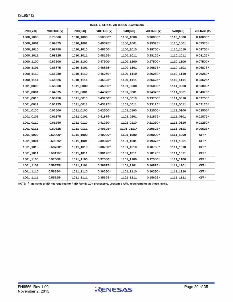
NOTE: * Indicates a VID not required for AMD Family 10h processors. Loosened AMD requirements at these levels.
TABLE 7. SERIAL VID CODES (Continued)
SVID[7:0] VOLTAGE (V) SVID[6:0] VOLTAGE (V) SVID[6:0] VOLTAGE (V) SVID[6:0] VOLTAGE (V)
FN8566 Rev 1.00 Page 20 of 35November 2, 2015
ISL95712
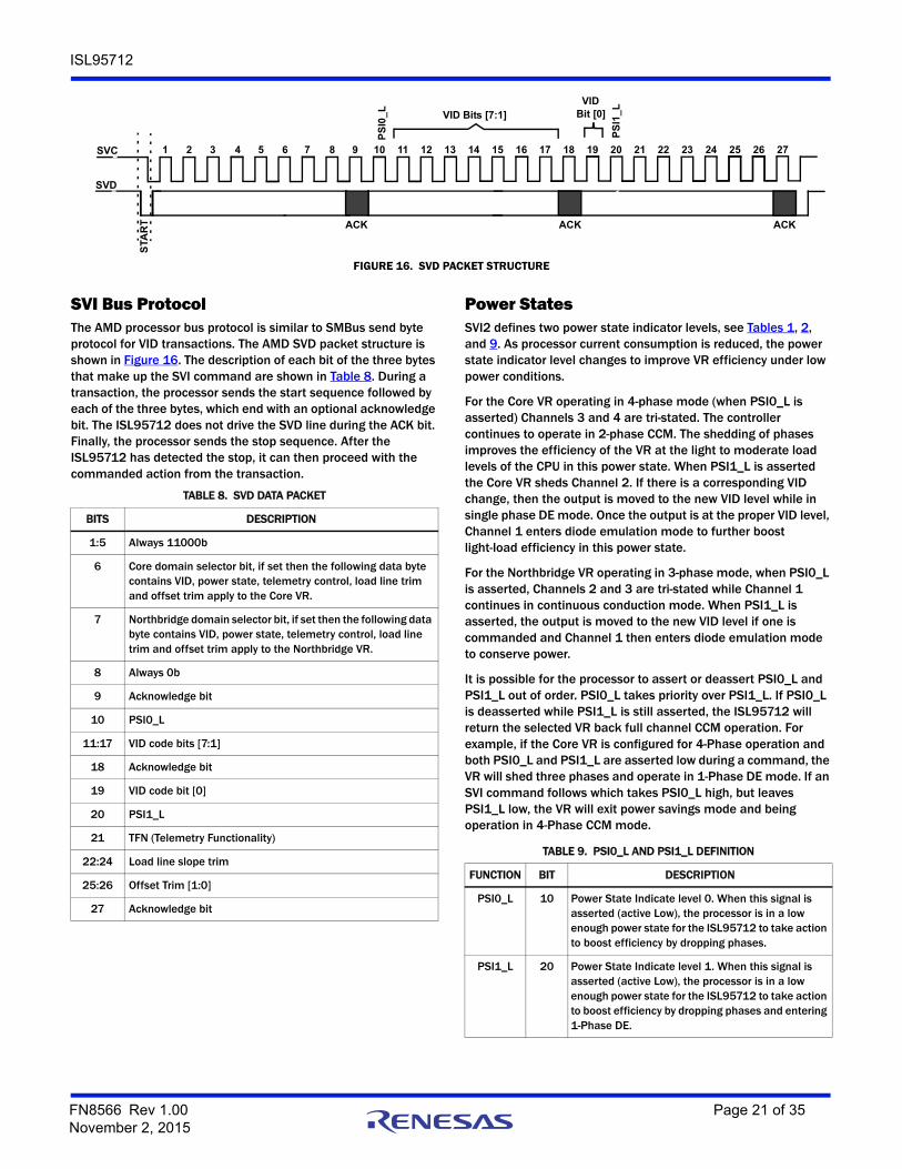
SVI Bus ProtocolThe AMD processor bus protocol is similar to SMBus send byte protocol for VID transactions. The AMD SVD packet structure is shown in Figure 16. The description of each bit of the three bytes that make up the SVI command are shown in Table 8. During a transaction, the processor sends the start sequence followed by each of the three bytes, which end with an optional acknowledge bit. The ISL95712 does not drive the SVD line during the ACK bit. Finally, the processor sends the stop sequence. After the ISL95712 has detected the stop, it can then proceed with the commanded action from the transaction.
Power StatesSVI2 defines two power state indicator levels, see Tables 1, 2, and 9. As processor current consumption is reduced, the power state indicator level changes to improve VR efficiency under low power conditions.
For the Core VR operating in 4-phase mode (when PSI0_L is asserted) Channels 3 and 4 are tri-stated. The controller continues to operate in 2-phase CCM. The shedding of phases improves the efficiency of the VR at the light to moderate load levels of the CPU in this power state. When PSI1_L is asserted the Core VR sheds Channel 2. If there is a corresponding VID change, then the output is moved to the new VID level while in single phase DE mode. Once the output is at the proper VID level, Channel 1 enters diode emulation mode to further boost light-load efficiency in this power state.
For the Northbridge VR operating in 3-phase mode, when PSI0_L is asserted, Channels 2 and 3 are tri-stated while Channel 1 continues in continuous conduction mode. When PSI1_L is asserted, the output is moved to the new VID level if one is commanded and Channel 1 then enters diode emulation mode to conserve power.
It is possible for the processor to assert or deassert PSI0_L and PSI1_L out of order. PSI0_L takes priority over PSI1_L. If PSI0_L is deasserted while PSI1_L is still asserted, the ISL95712 will return the selected VR back full channel CCM operation. For example, if the Core VR is configured for 4-Phase operation and both PSI0_L and PSI1_L are asserted low during a command, the VR will shed three phases and operate in 1-Phase DE mode. If an SVI command follows which takes PSI0_L high, but leaves PSI1_L low, the VR will exit power savings mode and being operation in 4-Phase CCM mode.
FIGURE 16. SVD PACKET STRUCTURE
1 2 3 4 5 6 7 12 14 15 16 171310
SVD
SVCS
TAR
T
PS
I1_
L
VID Bits [7:1]
118 9 18 19 20 21 22 23 24 25 26 27
VIDBit [0]
PS
I0_
L
ACK ACKACK
TABLE 8. SVD DATA PACKET
BITS DESCRIPTION
1:5 Always 11000b
6 Core domain selector bit, if set then the following data byte contains VID, power state, telemetry control, load line trim and offset trim apply to the Core VR.
7 Northbridge domain selector bit, if set then the following data byte contains VID, power state, telemetry control, load line trim and offset trim apply to the Northbridge VR.
8 Always 0b
9 Acknowledge bit
10 PSI0_L
11:17 VID code bits [7:1]
18 Acknowledge bit
19 VID code bit [0]
20 PSI1_L
21 TFN (Telemetry Functionality)
22:24 Load line slope trim
25:26 Offset Trim [1:0]
27 Acknowledge bit
TABLE 9. PSI0_L AND PSI1_L DEFINITION
FUNCTION BIT DESCRIPTION
PSI0_L 10 Power State Indicate level 0. When this signal is asserted (active Low), the processor is in a low enough power state for the ISL95712 to take action to boost efficiency by dropping phases.
PSI1_L 20 Power State Indicate level 1. When this signal is asserted (active Low), the processor is in a low enough power state for the ISL95712 to take action to boost efficiency by dropping phases and entering 1-Phase DE.
FN8566 Rev 1.00 Page 21 of 35November 2, 2015
ISL95712
Dynamic Load Line Slope TrimThe ISL95712 supports the SVI2 ability for the processor to manipulate the load line slope of the Core and Northbridge VRs independently using the serial VID interface. The slope manipulation applies to the initial load line slope. A load line slope trim will typically coincide with a VOTF change. See Table 10 for more information about the load line slope trim feature of the ISL95712. The Disable LL selection is not recommended unless operation without a LL is required and considered during the compensation of the VR.
Dynamic Offset TrimThe ISL95712 supports the SVI2 ability for the processor to manipulate the output voltage offset of the Core and Northbridge VRs. This offset is in addition to any output voltage offset set via the COMP resistor reader. The dynamic offset trim can disable the COMP resistor programmed offset of either output when Disable All Offset is selected.
TelemetryThe ISL95712 can provide voltage and current information to the AMD CPU through the telemetry system outlined by the AMD SVI2 specification. The telemetry data is transmitted through the SVC and SVT lines of the SVI2 interface.
Current telemetry is based on a voltage generated across a 133kΩ resistor placed from the IMON pin to GND. The current flowing out of the IMON pin is proportional to the load current in the VR. The Isum current defined in “Voltage Regulation and Load Line Implementation” on page 12, provides the base conversion from the load current to the internal amplifier created Isum current. The Isum current is then divided down by a factor of 4 to create the IMON current, which flows out of the IMON pin. The Isum current will measure 36µA when the load current is at full load based on a droop current designed for 45µA at the same load current. The difference between the Isum current and the droop current is provided in Equation 2. The IMON current will measure 11.25µA at full load current for the VR and the IMON voltage will be 1.2V. The load percentage, which is reported by the IC is based on the this voltage. When the load is 25% of the full load, the voltage on the IMON pin will be 25% of 1.2V or 0.3V.
The SVI interface allows the selection of no telemetry, voltage only, or voltage and current telemetry on either or both of the VR outputs. The TFN bit along with the Core and Northbridge domain selector bits are used by the processor to change the functionality of telemetry, see Table 12 for more information.
TABLE 10. LOAD LINE SLOPE TRIM DEFINITION
LOAD LINE SLOPE TRIM [2:0] DESCRIPTION
000 Disable LL
001 -40% mΩ Change
010 -20% mΩ Change
011 No Change
100 +20% mΩ Change
101 +40% mΩ Change
110 +60% mΩ Change
111 +80% mΩ Change
TABLE 11. OFFSET TRIM DEFINITION
OFFSET TRIM [1:0] DESCRIPTION
00 Disable All Offset
01 -25mV Change
10 0mV Change
11 +25mV Change
TABLE 12. TFN TRUTH TABLE
TFN, CORE, NB BITS [21, 6, 7] DESCRIPTION
1,0,1 Telemetry is in voltage and current mode. Therefore, voltage and current are sent for VDD and VDDNB domains by the controller.
1,0,0 Telemetry is in voltage mode only. Only the voltage of VDD and VDDNB domains is sent by the controller.
1,1,0 Telemetry is disabled.
1,1,1 Reserved
FN8566 Rev 1.00 Page 22 of 35November 2, 2015
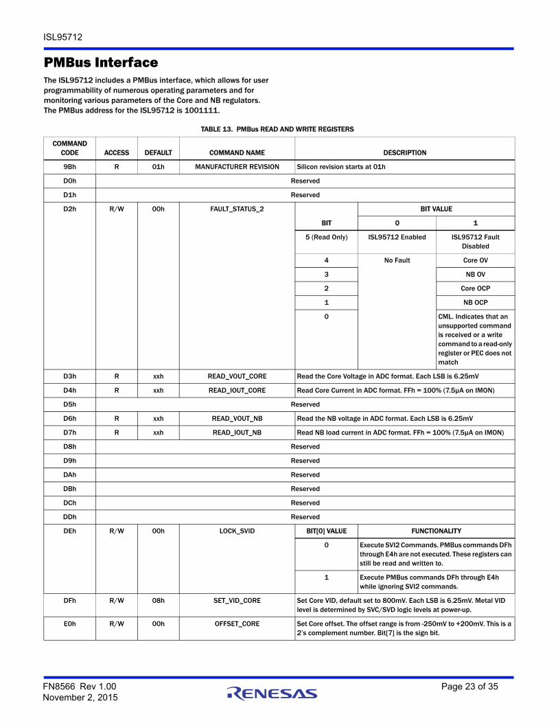
ISL95712
PMBus InterfaceThe ISL95712 includes a PMBus interface, which allows for user programmability of numerous operating parameters and for monitoring various parameters of the Core and NB regulators. The PMBus address for the ISL95712 is 1001111.
TABLE 13. PMBus READ AND WRITE REGISTERS
COMMAND CODE ACCESS DEFAULT COMMAND NAME DESCRIPTION
9Bh R 01h MANUFACTURER REVISION Silicon revision starts at 01h
D0h Reserved
D1h Reserved
D2h R/W 00h FAULT_STATUS_2
BIT
BIT VALUE
0 1
5 (Read Only) ISL95712 Enabled ISL95712 Fault Disabled
4 No Fault Core OV
3 NB OV
2 Core OCP
1 NB OCP
0 CML. Indicates that an unsupported command is received or a write command to a read-only register or PEC does not match
D3h R xxh READ_VOUT_CORE Read the Core Voltage in ADC format. Each LSB is 6.25mV
D4h R xxh READ_IOUT_CORE Read Core Current in ADC format. FFh = 100% (7.5µA on IMON)
D5h Reserved
D6h R xxh READ_VOUT_NB Read the NB voltage in ADC format. Each LSB is 6.25mV
D7h R xxh READ_IOUT_NB Read NB load current in ADC format. FFh = 100% (7.5µA on IMON)
D8h Reserved
D9h Reserved
DAh Reserved
DBh Reserved
DCh Reserved
DDh Reserved
DEh R/W 00h LOCK_SVID BIT[0] VALUE FUNCTIONALITY
0 Execute SVI2 Commands. PMBus commands DFh through E4h are not executed. These registers can still be read and written to.
1 Execute PMBus commands DFh through E4h while ignoring SVI2 commands.
DFh R/W 08h SET_VID_CORE Set Core VID, default set to 800mV. Each LSB is 6.25mV. Metal VID level is determined by SVC/SVD logic levels at power-up.
E0h R/W 00h OFFSET_CORE Set Core offset. The offset range is from -250mV to +200mV. This is a 2’s complement number. Bit[7] is the sign bit.
FN8566 Rev 1.00 Page 23 of 35November 2, 2015
ISL95712
Protection FeaturesCore VR and Northbridge VR both provide overcurrent, current-balance, undervoltage and overvoltage fault protections. The controller also provides over-temperature protection. The following discussion is based on Core VR and also applies to the Northbridge VR.
OvercurrentThe IMON voltage provides a means of determining the load current at any moment in time. The Overcurrent Protection (OCP) circuitry monitors the IMON voltage to determine when a fault occurs. Based on the previous description in “Voltage Regulation and Load Line Implementation” on page 12, the current which flows out of the IMON pin is proportional to the Isum current. The Isum current is created from the sensed voltage across Cn, which is a measure of the load current based upon the sensing element selected. The IMON current is generated internally and is 1/4 of the Isum current. The EDC or IDDspike current value for the AMD CPU load is used to set the maximum current level for droop and the IMON voltage of 1.2V, which indicates 100% loading for telemetry. The Isum current level at maximum load, or IDDspike, is 36µA and this translates to an IMON current level of 9µA. The IMON resistor is 133kΩ and the 9µA flowing through the IMON resistor results in a 1.2V level at maximum loading of the VR.
The overcurrent threshold is 1.5V on the IMON pin. Based on a 1.2V IMON voltage equating to 100% loading, the additional 0.3V provided above this level equates to a 25% increase in load current before an OCP fault is detected. The EDC or IDDspike current is used to set the 1.2V on IMON for full load current. Thus the OCP level is 1.25 times the EDC or IDDspike current level. This additional margin above the EDC or IDDspike current allows the AMD CPU to enter and exit the IDDspike performance mode without issue unless the load current is out of line with the IDDspike expectation, thus the need for overcurrent protection.
When the voltage on the IMON pin meets the overcurrent threshold of 1.5V, this triggers an OCP event. Within 2µs of detecting an OCP event, the controller asserts VR_HOT_L low to communicate to the AMD CPU to throttle back. A fault timer begins counting while IMON is at or above the 1.5V threshold. The fault timer lasts 7.5µs to 11µs and then the controller takes action by tri-stating the active channels. This provides the CPU time to recover and reduce the load current. If the OCP conditions are relieved, then the fault timer is cleared and VR_HOT_L is taken high clearing the fault condition. If the load current is not reduced and the OCP condition is maintained, the output voltage will fall below the undervoltage threshold due to the lack of switching or a way-overcurrent fault could occur. Either of these fault conditions will cause the controller to drop PGOOD of that output. When PGOOD is taken low, a fault flag from this VR is sent to the other VR and it is shut down within 10µs and PGOOD of the other output is taken low.
The ISL95712 also features a Way-Overcurrent [WOC] feature, which immediately takes the controller into shutdown. This protection is also referred to as fast overcurrent protection for short-circuit protection. If the IMON current reaches 15µA, WOC is triggered. Active channels are tri-stated and the controller is placed in shutdown and PGOOD is pulled low. There is no fault timer on the WOC fault, the controller takes immediate action. The other controller output is also shut down within 10µs.
Current-BalanceThe controller monitors the ISENx pin voltages to determine current-balance protection. If the ISENx pin voltage difference is greater than 9mV for 1ms, the controller will declare a fault and latch off.
E1h R/W 0fh LOADLINE_PWRSTATE_CORE BIT FUNCTIONALITY
[4:2] Load line slope trim. Refer to Table 10 for proper usage.
1 Sets PSI0 power state. Refer to Table 9 for proper usage.
0 Sets PSI1 power state. Refer to Table 9 for proper usage.
E2h R/W 08h SET_VID_NB Set NB VID, default set to 800mV. Each LSB is 6.25mV. Metal VID level is determined by SVC/SVD logic levels at power-up.
E3h R/W 00h OFFSET_NB Set NB offset. The offset range is from -250mV to +200mV. This is a 2’s complement number. Bit[7] is the sign bit.
E4h R/W 0fh LOADLINE_PWRSTATE_NB BIT FUNCTIONALITY
[4:2] Load line slope trim. Refer to Table 10 for proper usage.
1 Sets PSI0 power state. Refer to Table 9 for proper usage.
0 Sets PSI1 power state. Refer to Table 9 for proper usage.
TABLE 13. PMBus READ AND WRITE REGISTERS (Continued)
COMMAND CODE ACCESS DEFAULT COMMAND NAME DESCRIPTION
FN8566 Rev 1.00 Page 24 of 35November 2, 2015
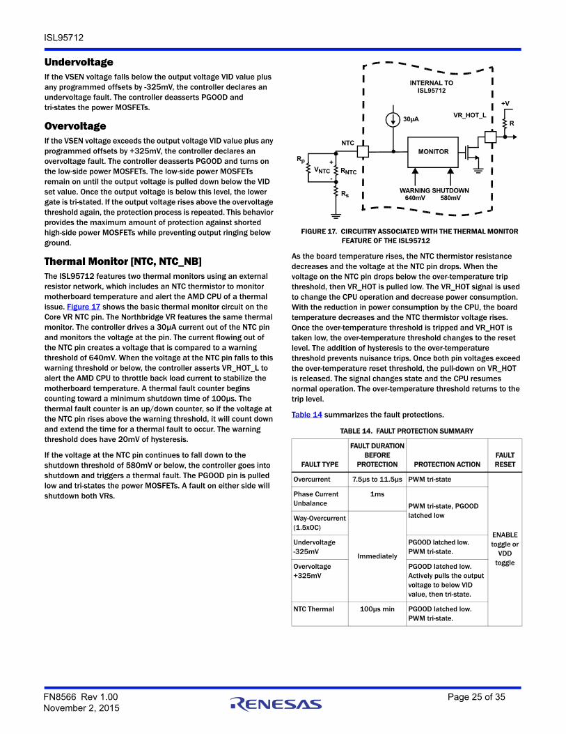
ISL95712
UndervoltageIf the VSEN voltage falls below the output voltage VID value plus any programmed offsets by -325mV, the controller declares an undervoltage fault. The controller deasserts PGOOD and tri-states the power MOSFETs.
OvervoltageIf the VSEN voltage exceeds the output voltage VID value plus any programmed offsets by +325mV, the controller declares an overvoltage fault. The controller deasserts PGOOD and turns on the low-side power MOSFETs. The low-side power MOSFETs remain on until the output voltage is pulled down below the VID set value. Once the output voltage is below this level, the lower gate is tri-stated. If the output voltage rises above the overvoltage threshold again, the protection process is repeated. This behavior provides the maximum amount of protection against shorted high-side power MOSFETs while preventing output ringing below ground.
Thermal Monitor [NTC, NTC_NB]The ISL95712 features two thermal monitors using an external resistor network, which includes an NTC thermistor to monitor motherboard temperature and alert the AMD CPU of a thermal issue. Figure 17 shows the basic thermal monitor circuit on the Core VR NTC pin. The Northbridge VR features the same thermal monitor. The controller drives a 30µA current out of the NTC pin and monitors the voltage at the pin. The current flowing out of the NTC pin creates a voltage that is compared to a warning threshold of 640mV. When the voltage at the NTC pin falls to this warning threshold or below, the controller asserts VR_HOT_L to alert the AMD CPU to throttle back load current to stabilize the motherboard temperature. A thermal fault counter begins counting toward a minimum shutdown time of 100µs. The thermal fault counter is an up/down counter, so if the voltage at the NTC pin rises above the warning threshold, it will count down and extend the time for a thermal fault to occur. The warning threshold does have 20mV of hysteresis.
If the voltage at the NTC pin continues to fall down to the shutdown threshold of 580mV or below, the controller goes into shutdown and triggers a thermal fault. The PGOOD pin is pulled low and tri-states the power MOSFETs. A fault on either side will shutdown both VRs.
As the board temperature rises, the NTC thermistor resistance decreases and the voltage at the NTC pin drops. When the voltage on the NTC pin drops below the over-temperature trip threshold, then VR_HOT is pulled low. The VR_HOT signal is used to change the CPU operation and decrease power consumption. With the reduction in power consumption by the CPU, the board temperature decreases and the NTC thermistor voltage rises. Once the over-temperature threshold is tripped and VR_HOT is taken low, the over-temperature threshold changes to the reset level. The addition of hysteresis to the over-temperature threshold prevents nuisance trips. Once both pin voltages exceed the over-temperature reset threshold, the pull-down on VR_HOT is released. The signal changes state and the CPU resumes normal operation. The over-temperature threshold returns to the trip level.
Table 14 summarizes the fault protections.
TABLE 14. FAULT PROTECTION SUMMARY
FAULT TYPE
FAULT DURATIONBEFORE
PROTECTION PROTECTION ACTIONFAULT RESET
Overcurrent 7.5µs to 11.5µs PWM tri-state
ENABLE toggle or
VDDtoggle
Phase Current Unbalance
1ms
PWM tri-state, PGOOD latched lowWay-Overcurrent
(1.5xOC)
Immediately
Undervoltage -325mV
PGOOD latched low. PWM tri-state.
Overvoltage +325mV
PGOOD latched low.Actively pulls the output voltage to below VID value, then tri-state.
NTC Thermal 100µs min PGOOD latched low.PWM tri-state.
NTC
RNTCVNTC-
+
30µA
INTERNAL TOISL95712
FIGURE 17. CIRCUITRY ASSOCIATED WITH THE THERMAL MONITOR FEATURE OF THE ISL95712
Rs
MONITOR
R
+V
Rp
WARNING640mV
SHUTDOWN580mV
VR_HOT_L
FN8566 Rev 1.00 Page 25 of 35November 2, 2015
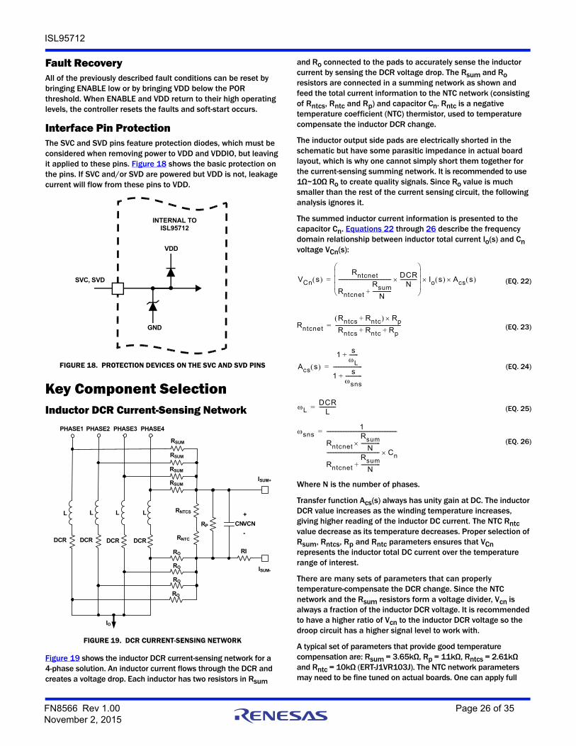
ISL95712
Fault RecoveryAll of the previously described fault conditions can be reset by bringing ENABLE low or by bringing VDD below the POR threshold. When ENABLE and VDD return to their high operating levels, the controller resets the faults and soft-start occurs.
Interface Pin ProtectionThe SVC and SVD pins feature protection diodes, which must be considered when removing power to VDD and VDDIO, but leaving it applied to these pins. Figure 18 shows the basic protection on the pins. If SVC and/or SVD are powered but VDD is not, leakage current will flow from these pins to VDD.
Key Component SelectionInductor DCR Current-Sensing Network
Figure 19 shows the inductor DCR current-sensing network for a 4-phase solution. An inductor current flows through the DCR and creates a voltage drop. Each inductor has two resistors in Rsum
and Ro connected to the pads to accurately sense the inductor current by sensing the DCR voltage drop. The Rsum and Ro resistors are connected in a summing network as shown and feed the total current information to the NTC network (consisting of Rntcs, Rntc and Rp) and capacitor Cn. Rntc is a negative temperature coefficient (NTC) thermistor, used to temperature compensate the inductor DCR change.
The inductor output side pads are electrically shorted in the schematic but have some parasitic impedance in actual board layout, which is why one cannot simply short them together for the current-sensing summing network. It is recommended to use 1Ω~10ΩRo to create quality signals. Since Ro value is much smaller than the rest of the current sensing circuit, the following analysis ignores it.
The summed inductor current information is presented to the capacitor Cn. Equations 22 through 26 describe the frequency domain relationship between inductor total current Io(s) and Cn voltage VCn(s):
Where N is the number of phases.
Transfer function Acs(s) always has unity gain at DC. The inductor DCR value increases as the winding temperature increases, giving higher reading of the inductor DC current. The NTC Rntc value decrease as its temperature decreases. Proper selection of Rsum, Rntcs, Rp and Rntc parameters ensures that VCn represents the inductor total DC current over the temperature range of interest.
There are many sets of parameters that can properly temperature-compensate the DCR change. Since the NTC network and the Rsum resistors form a voltage divider, Vcn is always a fraction of the inductor DCR voltage. It is recommended to have a higher ratio of Vcn to the inductor DCR voltage so the droop circuit has a higher signal level to work with.
A typical set of parameters that provide good temperature compensation are: Rsum = 3.65kΩ, Rp = 11kΩ, Rntcs = 2.61kΩ and Rntc = 10kΩ (ERT-J1VR103J). The NTC network parameters may need to be fine tuned on actual boards. One can apply full
SVC, SVD
INTERNAL TOISL95712
FIGURE 18. PROTECTION DEVICES ON THE SVC AND SVD PINS
GND
VDD
CN
RSUM
RO
RNTCS
RNTC
RP
DCR
L
DCR
L
RSUM
RO
PHASE2 PHASE3
IO
L
PHASE1
RO
RSUM
RI
VCN
+
-
L
PHASE4
RSUM
RO
DCRDCR
ISUM+
ISUM-
FIGURE 19. DCR CURRENT-SENSING NETWORK
VCn s Rntcnet
Rntcnet
RsumN
---------------+
------------------------------------------ DCRN
-------------
Io s Acs s = (EQ. 22)
Rntcnet
Rntcs Rntc+ Rp
Rntcs Rntc Rp+ +----------------------------------------------------= (EQ. 23)
Acs s
1sL-------+
1s
sns-------------+
-----------------------= (EQ. 24)
LDCR
L-------------= (EQ. 25)
sns1
Rntcnet
RsumN
---------------
Rntcnet
RsumN
---------------+
------------------------------------------ Cn
--------------------------------------------------------=(EQ. 26)
FN8566 Rev 1.00 Page 26 of 35November 2, 2015
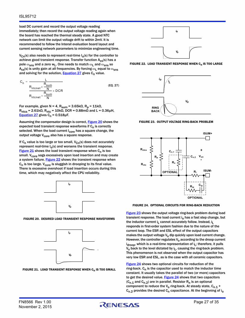
ISL95712
load DC current and record the output voltage reading immediately; then record the output voltage reading again when the board has reached the thermal steady state. A good NTC network can limit the output voltage drift to within 2mV. It is recommended to follow the Intersil evaluation board layout and current sensing network parameters to minimize engineering time.
VCn(s) also needs to represent real-time Io(s) for the controller to achieve good transient response. Transfer function Acs(s) has a pole sns and a zero wL. One needs to match L and sns so Acs(s) is unity gain at all frequencies. By forcing L equal to sns and solving for the solution, Equation 27 gives Cn value.
For example, given N = 4, Rsum = 3.65kΩ, Rp = 11kΩ, Rntcs = 2.61kΩ, Rntc = 10kΩ, DCR = 0.88mΩ and L = 0.36µH, Equation 27 gives Cn = 0.518µF.
Assuming the compensator design is correct, Figure 20 shows the expected load transient response waveforms if Cn is correctly selected. When the load current Icore has a square change, the output voltage Vcore also has a square response.
If Cn value is too large or too small, VCn(s) does not accurately represent real-time Io(s) and worsens the transient response. Figure 21 shows the load transient response when Cn is too small. Vcore sags excessively upon load insertion and may create a system failure. Figure 22 shows the transient response when Cn is too large. Vcore is sluggish in drooping to its final value. There is excessive overshoot if load insertion occurs during this time, which may negatively affect the CPU reliability.
Figure 23 shows the output voltage ring-back problem during load transient response. The load current io has a fast step change, but the inductor current iL cannot accurately follow. Instead, iL responds in first-order system fashion due to the nature of the current loop. The ESR and ESL effect of the output capacitors makes the output voltage Vo dip quickly upon load current change. However, the controller regulates Vo according to the droop current idroop, which is a real-time representation of iL; therefore, it pulls Vo back to the level dictated by iL, causing the ring-back problem. This phenomenon is not observed when the output capacitor has very low ESR and ESL, as is the case with all ceramic capacitors.
Figure 24 shows two optional circuits for reduction of the ring-back. Cn is the capacitor used to match the inductor time constant. It usually takes the parallel of two (or more) capacitors to get the desired value. Figure 24 shows that two capacitors (Cn.1 and Cn.2) are in parallel. Resistor Rn is an optional component to reduce the Vo ring-back. At steady state, Cn.1 + Cn.2 provides the desired Cn capacitance. At the beginning of io
CnL
Rntcnet
RsumN
---------------
Rntcnet
RsumN
---------------+
------------------------------------------ DCR
---------------------------------------------------------------=(EQ. 27)
FIGURE 20. DESIRED LOAD TRANSIENT RESPONSE WAVEFORMS
oi
Vo
FIGURE 21. LOAD TRANSIENT RESPONSE WHEN Cn IS TOO SMALL
oi
Vo
FIGURE 22. LOAD TRANSIENT RESPONSE WHEN Cn IS TOO LARGE
oi
Vo
FIGURE 23. OUTPUT VOLTAGE RING-BACK PROBLEM
oi
Vo
Li
RING BACK
FIGURE 24. OPTIONAL CIRCUITS FOR RING-BACK REDUCTION
Cn.2
Rntcs
Rntc
Rp
Ri
ISUM+
ISUM-
RipCip
OPTIONAL
Vcn
Cn.1
Rn
OPTIONAL
+
-
FN8566 Rev 1.00 Page 27 of 35November 2, 2015
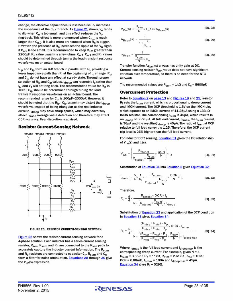
ISL95712
change, the effective capacitance is less because Rn increases the impedance of the Cn.1 branch. As Figure 21 shows, Vo tends to dip when Cn is too small, and this effect reduces the Vo ring-back. This effect is more pronounced when Cn.1 is much larger than Cn.2. It is also more pronounced when Rn is bigger. However, the presence of Rn increases the ripple of the Vn signal if Cn.2 is too small. It is recommended to keep Cn.2 greater than 2200pF. Rn value usually is a few ohms. Cn.1, Cn.2 and Rn values should be determined through tuning the load transient response waveforms on an actual board.
Rip and Cip form an R-C branch in parallel with Ri, providing a lower impedance path than Ri at the beginning of io change. Rip and Cip do not have any effect at steady state. Through proper selection of Rip and Cip values, idroop can resemble io rather than iL, and Vo will not ring back. The recommended value for Rip is 100Ω. Cip should be determined through tuning the load transient response waveforms on an actual board. The recommended range for Cip is 100pF~2000pF. However, it should be noted that the Rip - Cip branch may distort the idroop waveform. Instead of being triangular as the real inductor current, idroop may have sharp spikes, which may adversely affect idroop average value detection and therefore may affect OCP accuracy. User discretion is advised.
Resistor Current-Sensing Network
Figure 25 shows the resistor current-sensing network for a 4-phase solution. Each inductor has a series current sensing resistor, Rsen. Rsum and Ro are connected to the Rsen pads to accurately capture the inductor current information. The Rsum and Ro resistors are connected to capacitor Cn. Rsum and Cn form a filter for noise attenuation. Equations 28 through 30 give the VCn(s) expression.
Transfer function ARsen(s) always has unity gain at DC. Current-sensing resistor Rsen value does not have significant variation over-temperature, so there is no need for the NTC network.
The recommended values are Rsum = 1kΩ and Cn = 5600pF.
Overcurrent ProtectionRefer to Equation 2 on page 13 and Figures 19 and 25; resistor Ri sets the Isum current, which is proportional to droop current and IMON current. The OCP threshold is 1.5V on the IMON pin, which equates to an IMON current of 11.25µA using a 133kΩ IMON resistor. The corresponding Isum is 45µA, which results in an Idroop of 56.25µA. At full load current, Iomax, the Isum current is 36µA and the resulting Idroop is 45µA. The ratio of Isum at OCP relative to full load current is 1.25. Therefore, the OCP current trip level is 25% higher than the full load current.
For inductor DCR sensing, Equation 31 gives the DC relationship of Vcn(s) and Io(s):
Substitution of Equation 31 into Equation 2 gives Equation 32:
Therefore:
Substitution of Equation 23 and application of the OCP condition in Equation 33 gives Equation 34:
Where Iomax is the full load current and Idroopmax is the corresponding droop current. For example, given N = 4, Rsum = 3.65kΩ, Rp = 11kΩ, Rntcs = 2.61kΩ, Rntc = 10kΩ, DCR = 0.88mΩ, Iomax = 100A and Idroopmax = 45μA. Equation 34 gives Ri = 529Ω.
FIGURE 25. RESISTOR CURRENT-SENSING NETWORK
CN
RSUM
RO
DCR
L
DCR
L
RSUM
RO
PHASE2 PHASE3
IO
PHASE1
RO
RSUM
Ri
VCNRSEN RSEN +-
PHASE4
RSENRSEN
DCR
L
DCR
L
RSUM
RO
ISUM+
ISUM-
VCn s Rsen
N------------- Io s ARsen s = (EQ. 28)
ARsen s 1
1s
sns-------------+
-----------------------= (EQ. 29)
Rsen1
RsumN
--------------- Cn
-----------------------------= (EQ. 30)
VCn
Rntcnet
Rntcnet
RsumN
---------------+
------------------------------------------ DCRN
-------------
Io= (EQ. 31)
Idroop54--- 1
Ri-----
Rntcnet
Rntcnet
RsumN
---------------+
------------------------------------------ DCRN
------------- Io= (EQ. 32)
Ri54---
Rntcnet DCR Io
N Rntcnet
RsumN
---------------+ Idroop
----------------------------------------------------------------------------------= (EQ. 33)
Ri54---
Rntcs Rntc+ Rp
Rntcs Rntc Rp+ +---------------------------------------------------- DCR Iomax
NRntcs Rntc+ Rp
Rntcs Rntc Rp+ +----------------------------------------------------
RsumN
---------------+
Idroopmax
-----------------------------------------------------------------------------------------------------------------------------= (EQ. 34)
FN8566 Rev 1.00 Page 28 of 35November 2, 2015
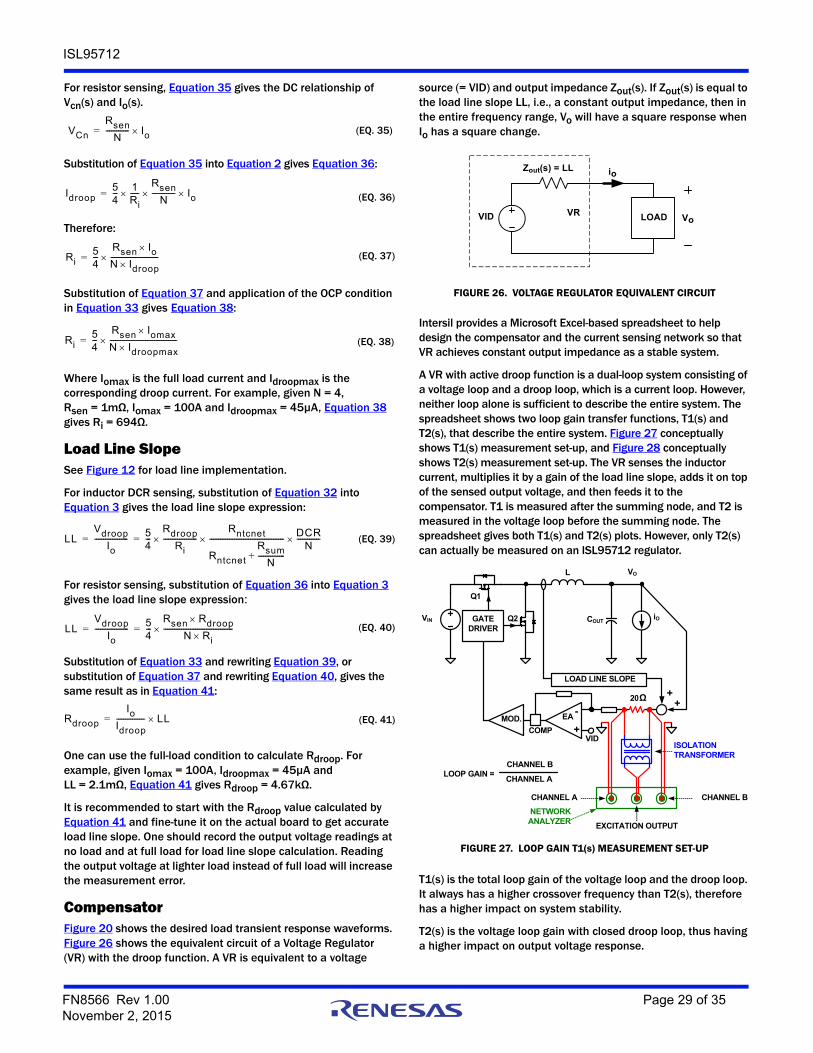
ISL95712
For resistor sensing, Equation 35 gives the DC relationship of Vcn(s) and Io(s).
Substitution of Equation 35 into Equation 2 gives Equation 36:
Therefore:
Substitution of Equation 37 and application of the OCP condition in Equation 33 gives Equation 38:
Where Iomax is the full load current and Idroopmax is the corresponding droop current. For example, given N = 4, Rsen = 1mΩ, Iomax = 100A and Idroopmax = 45µA, Equation 38 gives Ri = 694Ω.
Load Line SlopeSee Figure 12 for load line implementation.
For inductor DCR sensing, substitution of Equation 32 into Equation 3 gives the load line slope expression:
For resistor sensing, substitution of Equation 36 into Equation 3 gives the load line slope expression:
Substitution of Equation 33 and rewriting Equation 39, or substitution of Equation 37 and rewriting Equation 40, gives the same result as in Equation 41:
One can use the full-load condition to calculate Rdroop. For example, given Iomax = 100A, Idroopmax = 45µA and LL = 2.1mΩ, Equation 41 gives Rdroop = 4.67kΩ.
It is recommended to start with the Rdroop value calculated by Equation 41 and fine-tune it on the actual board to get accurate load line slope. One should record the output voltage readings at no load and at full load for load line slope calculation. Reading the output voltage at lighter load instead of full load will increase the measurement error.
CompensatorFigure 20 shows the desired load transient response waveforms. Figure 26 shows the equivalent circuit of a Voltage Regulator (VR) with the droop function. A VR is equivalent to a voltage
source (= VID) and output impedance Zout(s). If Zout(s) is equal to the load line slope LL, i.e., a constant output impedance, then in the entire frequency range, Vo will have a square response when Io has a square change.
Intersil provides a Microsoft Excel-based spreadsheet to help design the compensator and the current sensing network so that VR achieves constant output impedance as a stable system.
A VR with active droop function is a dual-loop system consisting of a voltage loop and a droop loop, which is a current loop. However, neither loop alone is sufficient to describe the entire system. The spreadsheet shows two loop gain transfer functions, T1(s) and T2(s), that describe the entire system. Figure 27 conceptually shows T1(s) measurement set-up, and Figure 28 conceptually shows T2(s) measurement set-up. The VR senses the inductor current, multiplies it by a gain of the load line slope, adds it on top of the sensed output voltage, and then feeds it to the compensator. T1 is measured after the summing node, and T2 is measured in the voltage loop before the summing node. The spreadsheet gives both T1(s) and T2(s) plots. However, only T2(s) can actually be measured on an ISL95712 regulator.
T1(s) is the total loop gain of the voltage loop and the droop loop. It always has a higher crossover frequency than T2(s), therefore has a higher impact on system stability.
T2(s) is the voltage loop gain with closed droop loop, thus having a higher impact on output voltage response.
VCn
RsenN
------------- Io= (EQ. 35)
Idroop54--- 1
Ri-----
RsenN
------------- Io= (EQ. 36)
Ri54---
Rsen Io
N Idroop---------------------------= (EQ. 37)
Ri54---
Rsen Iomax
N Idroopmax--------------------------------------= (EQ. 38)
LLVdroop
Io------------------- 5
4---
RdroopRi
-------------------Rntcnet
Rntcnet
RsumN
---------------+
------------------------------------------ DCRN
-------------= = (EQ. 39)
LLVdroop
Io------------------- 5
4---
Rsen Rdroop
N Ri---------------------------------------= = (EQ. 40)
Rdroop
IoIdroop---------------- LL= (EQ. 41)
FIGURE 26. VOLTAGE REGULATOR EQUIVALENT CIRCUIT
io
VoVID
Zout(s) = LL
LOADVR
FIGURE 27. LOOP GAIN T1(s) MEASUREMENT SET-UP
Q2
Q1
L
iOCOUT
VO
VIN GATE DRIVER
COMP
MOD.
LOAD LINE SLOPE
EA
VID
CHANNEL BCHANNEL A
EXCITATION OUTPUT
ISOLATION TRANSFORMER
20
LOOP GAIN =CHANNEL B
CHANNEL A
NETWORK ANALYZER
++
+
-Ω
FN8566 Rev 1.00 Page 29 of 35November 2, 2015
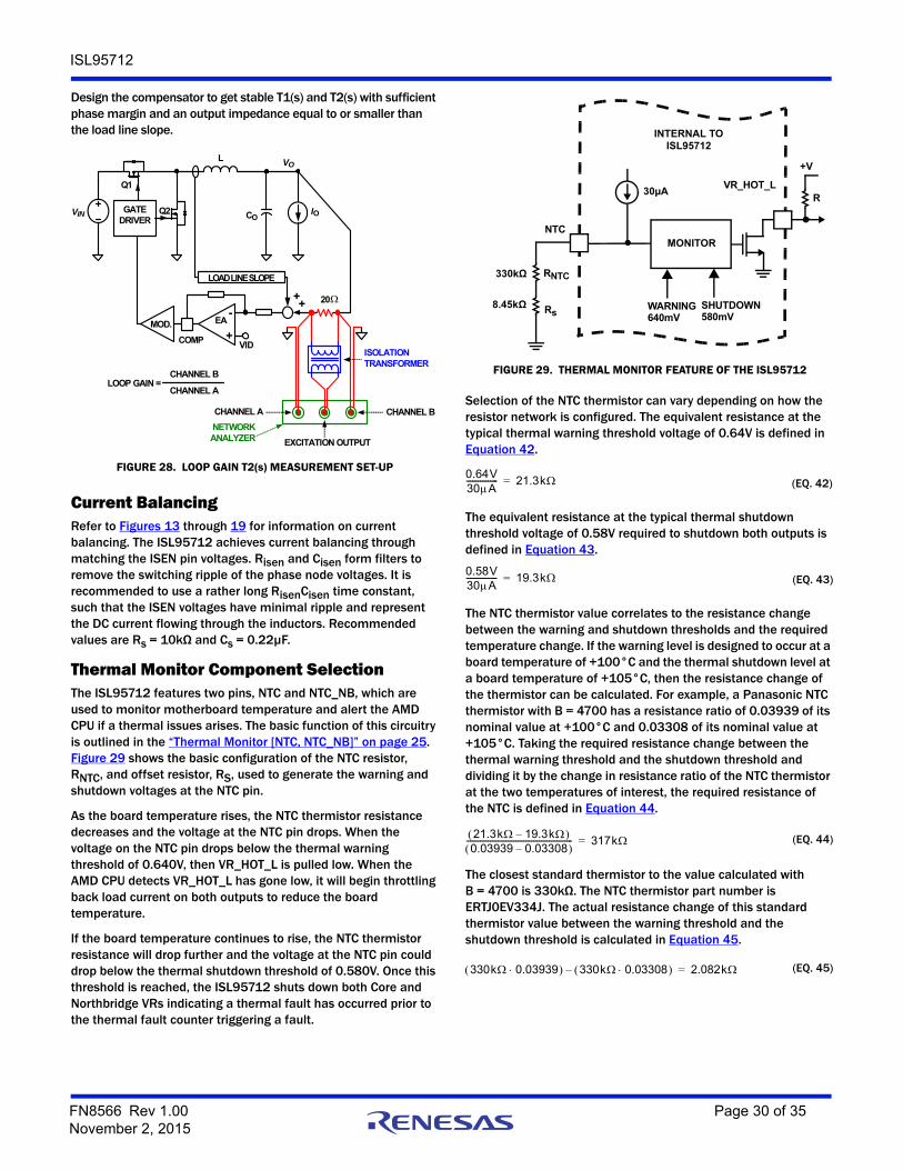
ISL95712
Design the compensator to get stable T1(s) and T2(s) with sufficient phase margin and an output impedance equal to or smaller than the load line slope.
Current BalancingRefer to Figures 13 through 19 for information on current balancing. The ISL95712 achieves current balancing through matching the ISEN pin voltages. Risen and Cisen form filters to remove the switching ripple of the phase node voltages. It is recommended to use a rather long RisenCisen time constant, such that the ISEN voltages have minimal ripple and represent the DC current flowing through the inductors. Recommended values are Rs = 10kΩ and Cs = 0.22µF.
Thermal Monitor Component SelectionThe ISL95712 features two pins, NTC and NTC_NB, which are used to monitor motherboard temperature and alert the AMD CPU if a thermal issues arises. The basic function of this circuitry is outlined in the “Thermal Monitor [NTC, NTC_NB]” on page 25. Figure 29 shows the basic configuration of the NTC resistor, RNTC, and offset resistor, RS, used to generate the warning and shutdown voltages at the NTC pin.
As the board temperature rises, the NTC thermistor resistance decreases and the voltage at the NTC pin drops. When the voltage on the NTC pin drops below the thermal warning threshold of 0.640V, then VR_HOT_L is pulled low. When the AMD CPU detects VR_HOT_L has gone low, it will begin throttling back load current on both outputs to reduce the board temperature.
If the board temperature continues to rise, the NTC thermistor resistance will drop further and the voltage at the NTC pin could drop below the thermal shutdown threshold of 0.580V. Once this threshold is reached, the ISL95712 shuts down both Core and Northbridge VRs indicating a thermal fault has occurred prior to the thermal fault counter triggering a fault.
Selection of the NTC thermistor can vary depending on how the resistor network is configured. The equivalent resistance at the typical thermal warning threshold voltage of 0.64V is defined in Equation 42.
The equivalent resistance at the typical thermal shutdown threshold voltage of 0.58V required to shutdown both outputs is defined in Equation 43.
The NTC thermistor value correlates to the resistance change between the warning and shutdown thresholds and the required temperature change. If the warning level is designed to occur at a board temperature of +100°C and the thermal shutdown level at a board temperature of +105°C, then the resistance change of the thermistor can be calculated. For example, a Panasonic NTC thermistor with B = 4700 has a resistance ratio of 0.03939 of its nominal value at +100°C and 0.03308 of its nominal value at +105°C. Taking the required resistance change between the thermal warning threshold and the shutdown threshold and dividing it by the change in resistance ratio of the NTC thermistor at the two temperatures of interest, the required resistance of the NTC is defined in Equation 44.
The closest standard thermistor to the value calculated with B = 4700 is 330kΩ. The NTC thermistor part number is ERTJ0EV334J. The actual resistance change of this standard thermistor value between the warning threshold and the shutdown threshold is calculated in Equation 45.
FIGURE 28. LOOP GAIN T2(s) MEASUREMENT SET-UP
Q2
Q1
L
IOCO
VO
VIN GATE DRIVER
COMP
MOD.
LOAD LINE SLOPE
EA
VID
CHANNEL BCHANNEL A
EXCITATION OUTPUT
ISOLATION TRANSFORMER
20
LOOP GAIN =CHANNEL B
CHANNEL A
NETWORK ANALYZER
++
+
-
NTC
RNTC
30µA
INTERNAL TOISL95712
FIGURE 29. THERMAL MONITOR FEATURE OF THE ISL95712
Rs
MONITOR
R
+V
WARNING640mV
SHUTDOWN580mV
VR_HOT_L
330kΩ
8.45kΩ
0.64V30A---------------- 21.3k= (EQ. 42)
0.58V30A---------------- 19.3k= (EQ. 43)
21.3k 19.3k– 0.03939 0.03308– ------------------------------------------------------ 317k= (EQ. 44)
330k 0.03939 330k 0.03308 – 2.082k= (EQ. 45)
FN8566 Rev 1.00 Page 30 of 35November 2, 2015
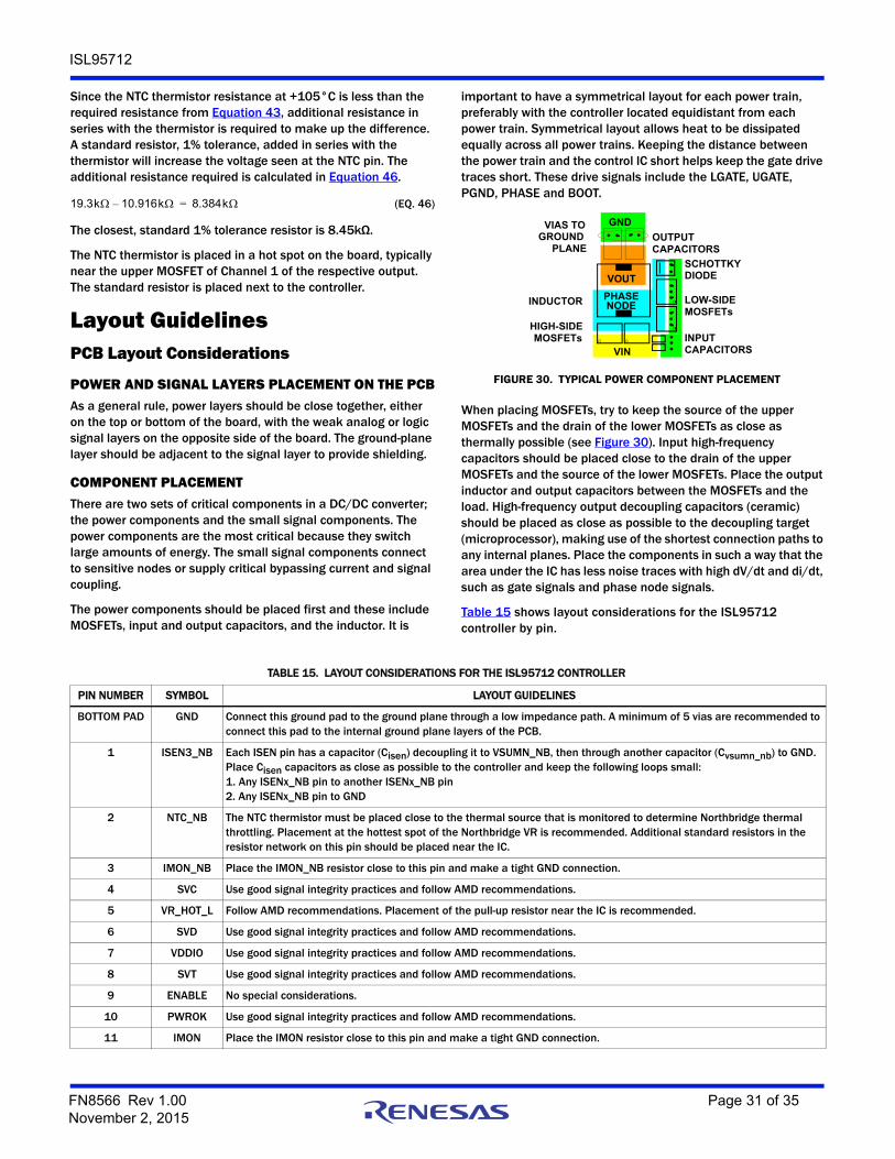
ISL95712
Since the NTC thermistor resistance at +105°C is less than the required resistance from Equation 43, additional resistance in series with the thermistor is required to make up the difference. A standard resistor, 1% tolerance, added in series with the thermistor will increase the voltage seen at the NTC pin. The additional resistance required is calculated in Equation 46.
The closest, standard 1% tolerance resistor is 8.45kΩ.
The NTC thermistor is placed in a hot spot on the board, typically near the upper MOSFET of Channel 1 of the respective output. The standard resistor is placed next to the controller.
Layout GuidelinesPCB Layout Considerations
POWER AND SIGNAL LAYERS PLACEMENT ON THE PCBAs a general rule, power layers should be close together, either on the top or bottom of the board, with the weak analog or logic signal layers on the opposite side of the board. The ground-plane layer should be adjacent to the signal layer to provide shielding.
COMPONENT PLACEMENTThere are two sets of critical components in a DC/DC converter; the power components and the small signal components. The power components are the most critical because they switch large amounts of energy. The small signal components connect to sensitive nodes or supply critical bypassing current and signal coupling.
The power components should be placed first and these include MOSFETs, input and output capacitors, and the inductor. It is
important to have a symmetrical layout for each power train, preferably with the controller located equidistant from each power train. Symmetrical layout allows heat to be dissipated equally across all power trains. Keeping the distance between the power train and the control IC short helps keep the gate drive traces short. These drive signals include the LGATE, UGATE, PGND, PHASE and BOOT.
When placing MOSFETs, try to keep the source of the upper MOSFETs and the drain of the lower MOSFETs as close as thermally possible (see Figure 30). Input high-frequency capacitors should be placed close to the drain of the upper MOSFETs and the source of the lower MOSFETs. Place the output inductor and output capacitors between the MOSFETs and the load. High-frequency output decoupling capacitors (ceramic) should be placed as close as possible to the decoupling target (microprocessor), making use of the shortest connection paths to any internal planes. Place the components in such a way that the area under the IC has less noise traces with high dV/dt and di/dt, such as gate signals and phase node signals.
Table 15 shows layout considerations for the ISL95712 controller by pin.
19.3k 10.916k– 8.384k= (EQ. 46)
FIGURE 30. TYPICAL POWER COMPONENT PLACEMENT
INDUCTOR
VIAS TO GROUND
PLANE
VIN
VOUT
PHASENODE
GND
OUTPUT CAPACITORS
LOW-SIDE MOSFETs
INPUT CAPACITORS
SCHOTTKYDIODE
HIGH-SIDE MOSFETs
TABLE 15. LAYOUT CONSIDERATIONS FOR THE ISL95712 CONTROLLER
PIN NUMBER SYMBOL LAYOUT GUIDELINES
BOTTOM PAD GND Connect this ground pad to the ground plane through a low impedance path. A minimum of 5 vias are recommended to connect this pad to the internal ground plane layers of the PCB.
1 ISEN3_NB Each ISEN pin has a capacitor (Cisen) decoupling it to VSUMN_NB, then through another capacitor (Cvsumn_nb) to GND. Place Cisen capacitors as close as possible to the controller and keep the following loops small:1. Any ISENx_NB pin to another ISENx_NB pin2. Any ISENx_NB pin to GND
2 NTC_NB The NTC thermistor must be placed close to the thermal source that is monitored to determine Northbridge thermal throttling. Placement at the hottest spot of the Northbridge VR is recommended. Additional standard resistors in the resistor network on this pin should be placed near the IC.
3 IMON_NB Place the IMON_NB resistor close to this pin and make a tight GND connection.
4 SVC Use good signal integrity practices and follow AMD recommendations.
5 VR_HOT_L Follow AMD recommendations. Placement of the pull-up resistor near the IC is recommended.
6 SVD Use good signal integrity practices and follow AMD recommendations.
7 VDDIO Use good signal integrity practices and follow AMD recommendations.
8 SVT Use good signal integrity practices and follow AMD recommendations.
9 ENABLE No special considerations.
10 PWROK Use good signal integrity practices and follow AMD recommendations.
11 IMON Place the IMON resistor close to this pin and make a tight GND connection.
FN8566 Rev 1.00 Page 31 of 35November 2, 2015
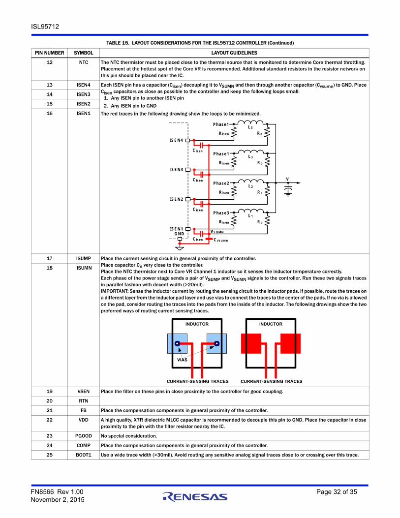
ISL95712
12 NTC The NTC thermistor must be placed close to the thermal source that is monitored to determine Core thermal throttling. Placement at the hottest spot of the Core VR is recommended. Additional standard resistors in the resistor network on this pin should be placed near the IC.
13 ISEN4 Each ISEN pin has a capacitor (Cisen) decoupling it to VSUMN and then through another capacitor (Cvsumn) to GND. Place Cisen capacitors as close as possible to the controller and keep the following loops small:
1. Any ISEN pin to another ISEN pin
2. Any ISEN pin to GND
The red traces in the following drawing show the loops to be minimized.
14 ISEN3
15 ISEN2
16 ISEN1
17 ISUMP Place the current sensing circuit in general proximity of the controller. Place capacitor Cn very close to the controller. Place the NTC thermistor next to Core VR Channel 1 inductor so it senses the inductor temperature correctly. Each phase of the power stage sends a pair of VSUMP and VSUMN signals to the controller. Run these two signals traces in parallel fashion with decent width (>20mil).IMPORTANT: Sense the inductor current by routing the sensing circuit to the inductor pads. If possible, route the traces on a different layer from the inductor pad layer and use vias to connect the traces to the center of the pads. If no via is allowed on the pad, consider routing the traces into the pads from the inside of the inductor. The following drawings show the two preferred ways of routing current sensing traces.
18 ISUMN
19 VSEN Place the filter on these pins in close proximity to the controller for good coupling.
20 RTN
21 FB Place the compensation components in general proximity of the controller.
22 VDD A high quality, X7R dielectric MLCC capacitor is recommended to decouple this pin to GND. Place the capacitor in close proximity to the pin with the filter resistor nearby the IC.
23 PGOOD No special consideration.
24 COMP Place the compensation components in general proximity of the controller.
25 BOOT1 Use a wide trace width (>30mil). Avoid routing any sensitive analog signal traces close to or crossing over this trace.
TABLE 15. LAYOUT CONSIDERATIONS FOR THE ISL95712 CONTROLLER (Continued)
PIN NUMBER SYMBOL LAYOUT GUIDELINES
V
IS E N 3
L 3
R is e n
IS E N 2
IS E N 1
L 2
L 1
R is e n
R is e n
P h a s e 1
P h a s e 2
P h a s e 3
R o
R o
R o
G N D
C is e n
C is e n
C is e n C v s u m n
V S U M N
IS E N 4
L 3
R is e n
P h a s e 1
R o
C is e n
INDUCTOR
CURRENT-SENSING TRACES
VIAS
INDUCTOR
CURRENT-SENSING TRACES
FN8566 Rev 1.00 Page 32 of 35November 2, 2015
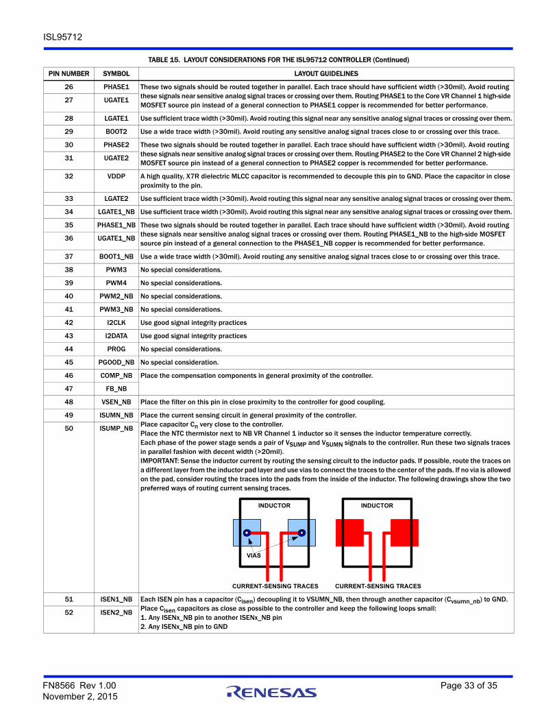
ISL95712
26 PHASE1 These two signals should be routed together in parallel. Each trace should have sufficient width (>30mil). Avoid routing these signals near sensitive analog signal traces or crossing over them. Routing PHASE1 to the Core VR Channel 1 high-side MOSFET source pin instead of a general connection to PHASE1 copper is recommended for better performance.
27 UGATE1
28 LGATE1 Use sufficient trace width (>30mil). Avoid routing this signal near any sensitive analog signal traces or crossing over them.
29 BOOT2 Use a wide trace width (>30mil). Avoid routing any sensitive analog signal traces close to or crossing over this trace.
30 PHASE2 These two signals should be routed together in parallel. Each trace should have sufficient width (>30mil). Avoid routing these signals near sensitive analog signal traces or crossing over them. Routing PHASE2 to the Core VR Channel 2 high-side MOSFET source pin instead of a general connection to PHASE2 copper is recommended for better performance.
31 UGATE2
32 VDDP A high quality, X7R dielectric MLCC capacitor is recommended to decouple this pin to GND. Place the capacitor in close proximity to the pin.
33 LGATE2 Use sufficient trace width (>30mil). Avoid routing this signal near any sensitive analog signal traces or crossing over them.
34 LGATE1_NB Use sufficient trace width (>30mil). Avoid routing this signal near any sensitive analog signal traces or crossing over them.
35 PHASE1_NB These two signals should be routed together in parallel. Each trace should have sufficient width (>30mil). Avoid routing these signals near sensitive analog signal traces or crossing over them. Routing PHASE1_NB to the high-side MOSFET source pin instead of a general connection to the PHASE1_NB copper is recommended for better performance.
36 UGATE1_NB
37 BOOT1_NB Use a wide trace width (>30mil). Avoid routing any sensitive analog signal traces close to or crossing over this trace.
38 PWM3 No special considerations.
39 PWM4 No special considerations.
40 PWM2_NB No special considerations.
41 PWM3_NB No special considerations.
42 I2CLK Use good signal integrity practices
43 I2DATA Use good signal integrity practices
44 PROG No special considerations.
45 PGOOD_NB No special consideration.
46 COMP_NB Place the compensation components in general proximity of the controller.
47 FB_NB
48 VSEN_NB Place the filter on this pin in close proximity to the controller for good coupling.
49 ISUMN_NB Place the current sensing circuit in general proximity of the controller. Place capacitor Cn very close to the controller. Place the NTC thermistor next to NB VR Channel 1 inductor so it senses the inductor temperature correctly. Each phase of the power stage sends a pair of VSUMP and VSUMN signals to the controller. Run these two signals traces in parallel fashion with decent width (>20mil).IMPORTANT: Sense the inductor current by routing the sensing circuit to the inductor pads. If possible, route the traces on a different layer from the inductor pad layer and use vias to connect the traces to the center of the pads. If no via is allowed on the pad, consider routing the traces into the pads from the inside of the inductor. The following drawings show the two preferred ways of routing current sensing traces.
50 ISUMP_NB
51 ISEN1_NB Each ISEN pin has a capacitor (Cisen) decoupling it to VSUMN_NB, then through another capacitor (Cvsumn_nb) to GND. Place Cisen capacitors as close as possible to the controller and keep the following loops small:1. Any ISENx_NB pin to another ISENx_NB pin2. Any ISENx_NB pin to GND
52 ISEN2_NB
TABLE 15. LAYOUT CONSIDERATIONS FOR THE ISL95712 CONTROLLER (Continued)
PIN NUMBER SYMBOL LAYOUT GUIDELINES
INDUCTOR
CURRENT-SENSING TRACES
VIAS
INDUCTOR
CURRENT-SENSING TRACES
FN8566 Rev 1.00 Page 33 of 35November 2, 2015
ISL95712
Intersil products are manufactured, assembled and tested utilizing ISO9001 quality systems as notedin the quality certifications found at www.intersil.com/en/support/qualandreliability.html
Intersil products are sold by description only. Intersil may modify the circuit design and/or specifications of products at any time without notice, provided that such modification does not, in Intersil's sole judgment, affect the form, fit or function of the product. Accordingly, the reader is cautioned to verify that datasheets are current before placing orders. Information furnished by Intersil is believed to be accurate and reliable. However, no responsibility is assumed by Intersil or its subsidiaries for its use; nor for any infringements of patents or other rights of third parties which may result from its use. No license is granted by implication or otherwise under any patent or patent rights of Intersil or its subsidiaries.
For information regarding Intersil Corporation and its products, see www.intersil.com
For additional products, see www.intersil.com/en/products.html
© Copyright Intersil Americas LLC 2014-2015. All Rights Reserved.All trademarks and registered trademarks are the property of their respective owners.
About IntersilIntersil Corporation is a leading provider of innovative power management and precision analog solutions. The company's products address some of the largest markets within the industrial and infrastructure, mobile computing and high-end consumer markets.
For the most updated datasheet, application notes, related documentation and related parts, please see the respective product information page found at www.intersil.com.
You may report errors or suggestions for improving this datasheet by visiting www.intersil.com/ask.
Reliability reports are also available from our website at www.intersil.com/support.
Revision HistoryThe revision history provided is for informational purposes only and is believed to be accurate, but not warranted. Please go to web to make sure you have the latest revision.
DATE REVISION CHANGE
November 2, 2015 FN8566.1 On page 1 under Features, added “Serial VID clock frequency range 100kHz to 25MHz” below “Supports AMD SVI 2.0 serial data bus interface and PMBus”.Updated Package Outline Drawing L52.6X6A to the latest revision. Changes are as follows:
-Added tolerance ± values.
March 26, 2014 FN8566.0 Initial Release
FN8566 Rev 1.00 Page 34 of 35November 2, 2015
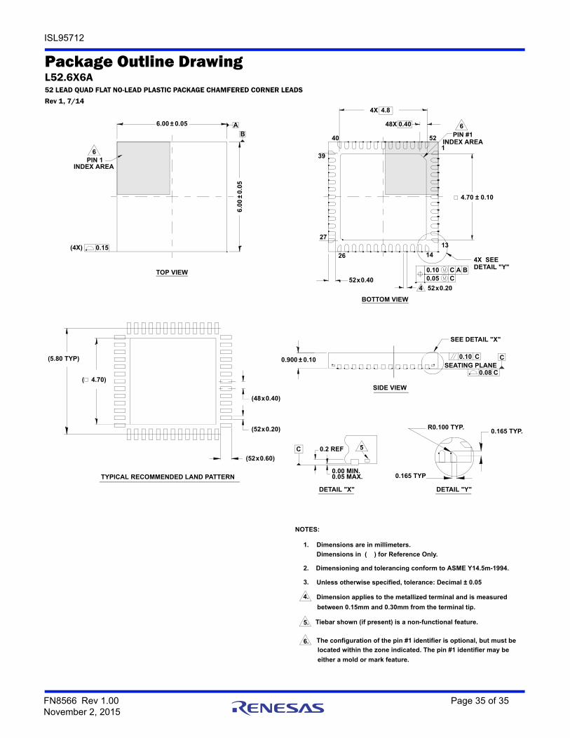
ISL95712
FN8566 Rev 1.00 Page 35 of 35November 2, 2015
Package Outline DrawingL52.6X6A52 LEAD QUAD FLAT NO-LEAD PLASTIC PACKAGE CHAMFERED CORNER LEADS
Rev 1, 7/14
BOTTOM VIEW
DETAIL "X"
SIDE VIEW
TYPICAL RECOMMENDED LAND PATTERN
TOP VIEW
located within the zone indicated. The pin #1 identifier may be
Unless otherwise specified, tolerance: Decimal ± 0.05
Tiebar shown (if present) is a non-functional feature.
The configuration of the pin #1 identifier is optional, but must be
between 0.15mm and 0.30mm from the terminal tip.
Dimension applies to the metallized terminal and is measured
Dimensions in ( ) for Reference Only.
Dimensioning and tolerancing conform to ASME Y14.5m-1994.
6.
either a mold or mark feature.
3.
5.
4.
2.
Dimensions are in millimeters.1.
NOTES:
(48x0.40)
(52x0.20)
(5.80 TYP)
( 4.70)
(52x0.60)
INDEX AREA
(4X) 0.15
PIN 16
AB
C
0.900 ± 0.10
0.2 REF
0.05 MAX.0.00 MIN.
5
SEATING PLANE0.10 C
0.08 C
C
52x0.40
27
26 14
39
40
0.4048X
4X 4.8
52
13
SEE DETAIL "X"
52x0.204
4.70 ± 0.10
PIN #16
1
0.165 TYP.R0.100 TYP.
0.165 TYP
4X SEE
INDEX AREA
0.10 C A B0.05 C
DETAIL "Y"
DETAIL "Y"
6.00 ± 0.05
6.0
0±
0.0
5