Embed Size (px)
Citation preview

MSE 421/521 Introduction to Electron Microscopy
R. Ubic
IV. The Transmission Electron Microscope A. The instrument The first transmission electron microscope was invented in 1933 by Max Knoll and Ernst Ruska at the Technical College in Berlin. The transmission electron microscope is the electronic cousin of the transmission light microscope: a beam of electrons passes through a thin sample followed by a series of lenses, forming a highly magnified image of the sample on a screen. Knoll and Ruska found that they could focus their electron beam with a magnetic lens that was produced by sending the beam through a current-carrying coil. Modern transmission electron microscopes usually consist of a beam column that is about 2.5m tall with a diameter of about 30cm, and they are able to achieve a resolution of about 2Å; however, the addition of aberration correctors has more than doubled this performance.
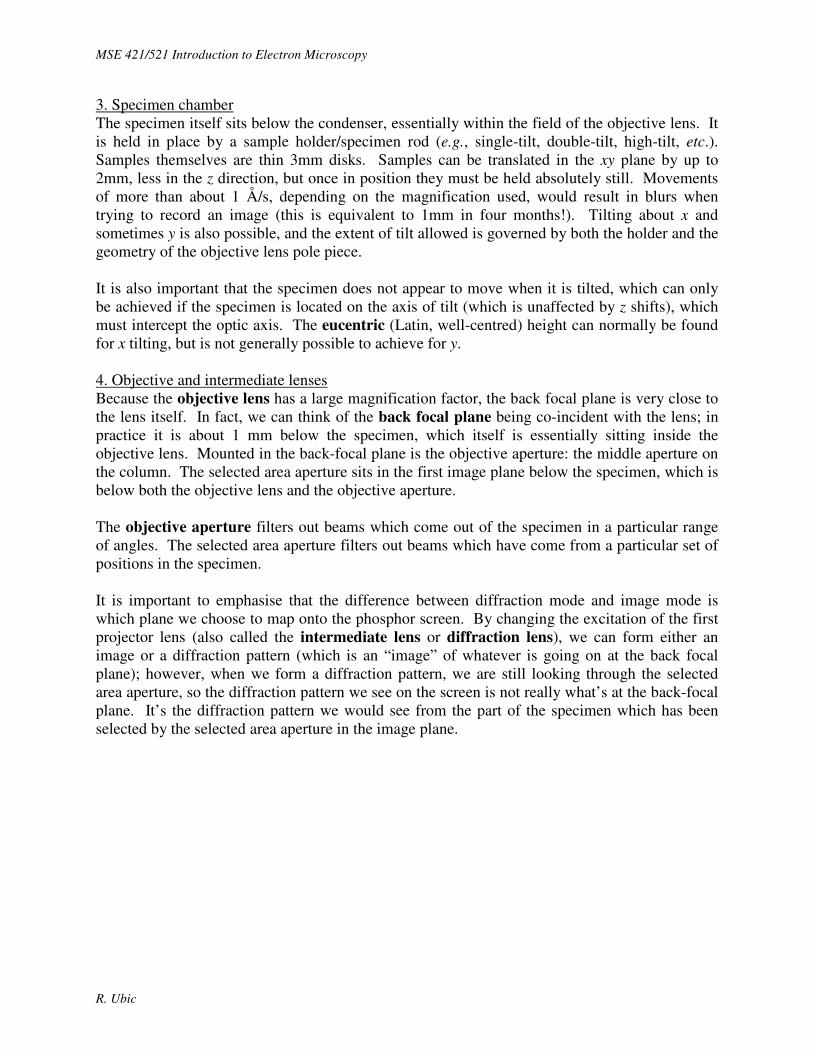
Source
First condenser lens, C1 (Spot Size)
Second condenser lens, C2 (Brightness)Condenser aperture
Specimen
First demagnified source image
Objective lens
Back focal plane
First image plane
Projector Lens(es)
Intermediate or diffraction lens
Objective aperture
Second image plane
Screen
Selected area aperture

MSE 421/521 Introduction to Electron Microscopy
R. Ubic
1. Electron gun At the top of the column, the electron gun† delivers high-energy electrons to the instrument. Thermionic guns (tungsten or LaB6) are the most common types. The appropriate electron energy depends on the nature of the specimen and the kind of information required. Higher electron energies allow thicker samples to be analysed and, due to their smaller wavelengths, increase the resolution possible; however, it is rare now to see TEMs which operate at energies greater than 200 keV. The introduction of field emission guns and improvements in lens design have largely made higher-energy microscopes unnecessary for high-resolution. Additionally, higher energy electrons cause increasing amounts of damage to samples. Biological samples in particular require lower operating voltages. 2. Condenser lens system The condenser lens system then acts to control and reduce the diameter of this beam. The first condenser C1 lens (or spot size) is a strong lens which demagnifies the image of the electron source by about X1/100 to give a small “point” source at the “crossover” which is more coherent than the large (50 µm diameter) filament tip. The second condenser C2 lens (brightness or intensity) is a weaker lens which projects the demagnified source image onto the specimen with a magnification of X2, giving an overall demagnification of X1/50. This lens controls the spread of illumination on the screen. The condenser aperture, located just below the condenser lenses (sometimes between them), collimates (makes parallel) the electron beam and modifies its intensity. Three parameters control the operation of the electron gun: the accelerating voltage, the filament current (and hence its temperature), and the bias voltage on the Wehnelt cap. The filament current controls the filament tip temperature and hence the number of electrons emitted . The emission is maximised by saturating the filament, i.e., increasing the filament current until the number of electrons emitted no longer increases. Ramping the filament current to saturation is controlled electronically on the JEOL 2100 and should not need to be adjusted by users. The gun bias controls the bias resistor setting, which controls the current passing between the high-voltage system and earth. At low bias values, the negative potential of the Wehnelt compared to the filament is ineffective; therefore, the electrons are accelerated towards the anode with relatively little focusing. The beam is consequently spread and appears weak on the screen. As the bias is increased, the focusing action improves so that the effective beam brightness increases; however, above a certain value the Wehnelt is so negative with respect to the filament that the brightness starts to decrease because electrons are prevented from being emitted from the filament or, if they are emitted, are repelled back towards the filament. The distance between the Wehnelt and the filament is obviously important in determining the point at which the optimum beam brightness is obtained. For this reason, if the filament has recently been changed, a slightly different emission setting may be required. † Never try taking one of these through airport security!
MSE 421/521 Introduction to Electron Microscopy
R. Ubic
3. Specimen chamber The specimen itself sits below the condenser, essentially within the field of the objective lens. It is held in place by a sample holder/specimen rod (e.g., single-tilt, double-tilt, high-tilt, etc.). Samples themselves are thin 3mm disks. Samples can be translated in the xy plane by up to 2mm, less in the z direction, but once in position they must be held absolutely still. Movements of more than about 1 Å/s, depending on the magnification used, would result in blurs when trying to record an image (this is equivalent to 1mm in four months!). Tilting about x and sometimes y is also possible, and the extent of tilt allowed is governed by both the holder and the geometry of the objective lens pole piece. It is also important that the specimen does not appear to move when it is tilted, which can only be achieved if the specimen is located on the axis of tilt (which is unaffected by z shifts), which must intercept the optic axis. The eucentric (Latin, well-centred) height can normally be found for x tilting, but is not generally possible to achieve for y. 4. Objective and intermediate lenses Because the objective lens has a large magnification factor, the back focal plane is very close to the lens itself. In fact, we can think of the back focal plane being co-incident with the lens; in practice it is about 1 mm below the specimen, which itself is essentially sitting inside the objective lens. Mounted in the back-focal plane is the objective aperture: the middle aperture on the column. The selected area aperture sits in the first image plane below the specimen, which is below both the objective lens and the objective aperture. The objective aperture filters out beams which come out of the specimen in a particular range of angles. The selected area aperture filters out beams which have come from a particular set of positions in the specimen. It is important to emphasise that the difference between diffraction mode and image mode is which plane we choose to map onto the phosphor screen. By changing the excitation of the first projector lens (also called the intermediate lens or diffraction lens), we can form either an image or a diffraction pattern (which is an “image” of whatever is going on at the back focal plane); however, when we form a diffraction pattern, we are still looking through the selected area aperture, so the diffraction pattern we see on the screen is not really what’s at the back-focal plane. It’s the diffraction pattern we would see from the part of the specimen which has been selected by the selected area aperture in the image plane.
MSE 421/521 Introduction to Electron Microscopy
R. Ubic
First demagnified source image
Back focal plane
First image plane
Second image plane
Source
First condenser lens, C1 (Spot Size)
Second condenser lens, C2 (Brightness)Condenser aperture
Specimen
Objective lens
Objective aperture
Intermediate or diffraction lens
Projector Lens(es)
Screenimage diffraction
pattern
Selected area aperture
5. Practical notes The value of the filament saturation will generally decrease with time as the filament material (W, LaB6, etc.) evaporates, making the filament smaller. Very low settings of the filament control are often a sign of imminent failure. On the JEOL 2100 the optimum emission setting is often about 63%. Never operate the microscope above this pre-set value. Contamination (“poisoning”) of the filament is also a potential problem. It is very important to maintain a good vacuum in the gun area. Contamination causes high-voltage break-down (arcing) which is manifest as voltage instability or complete shut-down caused by the loss of vacuum as particles of contamination are vaporised. In addition, a poor vacuum might cause oxidation of a W filament. Only ever turn on the electron beam when there is a good vacuum in the column (≤ 2.5 x 10⁻⁵Pa). Similarly, the gun area should be allowed to cool before the column is brought up to atmospheric pressure (this should only be done by BSCMC personnel). All parts of the gun area should be handled using appropriate gloves. There is no guarantee that when the filament has been changed that it points directly down the optic axis. Clearly, the beam must be on the optic axis to maximise brightness. On the JEOL 2100 the beam is centred using the gun tilt controls.

MSE 421/521 Introduction to Electron Microscopy
R. Ubic
6. Vacuum System Electron microscopes are operated under vacuum for four reasons:
- Because electrons scatter easily, the mean free path of electrons at atmospheric pressure is only about 1cm; however, at 10-6 Pa they can travel about 6.5m. - The vacuum acts as an insulator between the anode and cathode (filament) and in the area around the field emitters, thus hindering unwanted electrical discharge in the electron gun. - The elimination of oxygen around the filament prevents it from being oxidised and eventually “burning out.” - Reduced interaction between the electron beam and gas molecules decreases contamination on the sample.
The SI unit of pressure is the Pascal (Pa). Unfortunately, there are several other units for pressure also in common use. For convenience, a conversion chart is shown below. A further complication is that, despite the fact that vacuums necessarily require low pressures, we perversely refer to very low pressures as high vacuums!
1 atm 1 bar 760 mm Hg 760 Torr 101325 Pa 14.696 psi Different levels of vacuum are required for different parts of the microscope. The gun might require 10-9 Pa, while the specimen can be at 10-6 Pa and the projection chamber and camera can be at 10-5 Pa. There are three main types of vacuum pump: roughing pumps, high-vacuum pumps which need backing, and high-vacuum pumps which do not need backing. Alternatively, vacuums can be categorise vacuums as rough (100 - 0.1 Pa), low (10-1 - 10-4 Pa), high (10-4 - 10-7 Pa), or ultrahigh (< 10-7 Pa). a. Roughing Pump (Rotary Pump) A rotary pump can pump down from atmospheric pressure but can only reach a rather modest vacuum, at best about 1 - 0.1 Pa. They consist of a belt-driven, eccentrically mounted reciprocating mechanism suck air through an inlet valve into a chamber and expels it through an exit valve. Oil is typically used as a lubricant and gas seal, although expensive oil-free models are also available. The high-pressure side can operate at atmospheric pressures, while the low-pressure side is usually limited by the vapour pressure of the pump oil used. These pumps are generally reliable, inexpensive, noisy, and dirty.

MSE 421/521 Introduction to Electron Microscopy
R. Ubic
It is used to pump the chamber from ‘air’ (atmospheric pressure) when necessary, to pump the specimen transfer chamber (also from atmospheric pressure), and to back the diffusion pump. Because it is used to do so many things, it is usually attached to a roughing manifold, which is a pipe with lots of other pipes coming off it. By opening and closing various valves off the roughing manifold, the roughing pump can be switched from one role to another.
b. Diffusion Pump The most common type of pump for use in high vacuum applications is the diffusion pump (or, more properly, vapor jet pump). Diffusion pumps are one of the oldest and most reliable ways of creating a vacuum down to 10-7 Pa at room temperature.
A diffusion pump cannot begin its work with full atmospheric pressure inside the chamber. Instead, an ancillary mechanical rotary pump (or forepump), capable of a modest level of pumping, first brings the pressure inside the chamber down to about 10-1 Pa. At this point, the diffusion pump takes over to create a vacuum ranging from 10-1 to 10-8 Pa. Since the diffusion

MSE 421/521 Introduction to Electron Microscopy
R. Ubic
pump cannot exhaust directly to atmospheric pressure, the forepump is used to maintain proper discharge pressure conditions. Diffusion pumps use a high velocity stream of molecules to kinetically ‘trap’ random gas molecules from the vacuum system that blunder into the stream. They basically consist of a stainless steel chamber containing vertically stacked cone-shaped jet assemblies, each of which will support pressure ratios of approximately 10:1 or greater. Typically there are three jet assemblies of diminishing sizes, with the largest at the bottom. The pressure on the low-pressure side is typically around 10-4 Pa or so, while the maximum pressure on the high pressure side is typically on the order of around 7 Pa. At the base of the chamber is a pool of a specialized type of oil having a low vapour pressure. The oil is heated to boiling by an electric heater beneath the floor of the chamber. The vaporized oil moves upward and is expelled through the jets in the various assemblies. The high-energy oil droplets travel downward in the space between the jet assemblies and the chamber wall at speeds up to 335 ms-1. The droplets may actually exceed the speed of sound, but thankfully there is no sonic boom because the molecules in the partial vacuum are too far apart to transmit the sound energy. The capture efficiency of the vapour jet depends on its density, velocity, and molecular weight. The high-velocity jet collides with gas molecules that happen to enter it due to their thermal motion. This typically imparts a downward motion to the molecules and transports them towards the pump outlet, creating higher vacuum at the top of the pump chamber which is connected to the microscope column. At the base of the chamber, the condensed molecules of atmospheric gases are removed by the forepump, while the condensed oil begins another cycle. Water circulated through coils on the outside of the chamber cool it to prevent thermal runaway and permit operation over long periods of time. The first designs of diffusion pumps go back to 1915, when the pump was invented by Irving Langmuir. The original diffusion pump fluid used was mercury, which could withstand elevated temperatures but had the disadvantage of being toxic - and volatile. Indeed, the oil in a modern diffusion pump would contaminate the vacuum in the TEM if oil vapor were to escape into the column. To minimize this problem, several kinds of synthetic non-hydrocarbon oils with low vapour pressures, based on silicones, esters, perfluorals, and polyphenyl ethers, can be used. The polyphenyl ether Santovac® 5 and the perfluorinated polyethers Fomblin® and Krytox® have been worldwide standards for some time. These oils are expensive ($1-$2 per ml) and may eventually crack or char (oxidise) if subjected to both high temperature and pressure, forming a tar-like substance that can be extremely difficult to remove. Exactly what happens when diffusion pump oil cracks depends on the type of oil in the chamber and the temperature at which it breaks down. Breakdowns with hydrocarbon-based oils are hardest to clean up. The residue is much like tar and is tenacious. Silicone-based oils leave a residue that is somewhat easier to remove. Oils containing perfluorals decompose to form fluorine compounds that can be extremely toxic and very damaging to the aluminum jet assemblies. The least messy and least damaging are the polyphenyl ethers, in part because their breakdown temperature is much higher (350°C vs 300°C), and in part because polyphenyl ethers tend to decompose into small non-toxic molecules such as water and carbon dioxide. Thankfully, breakdowns involving polyphenyl ethers are rare.

MSE 421/521 Introduction to Electron Microscopy
R. Ubic
The diffusion pump is usually positioned at the bottom of the column, near the back. It is used to pump the viewing chamber and the photographic film casement. There is usually a large empty volume between the back end of the diffusion pump and the roughing manifold, so that when the microscope is being used, the roughing pump can be switched off (it creates a lot of vibration). The empty volume is very slowly filled with the gas being pumped out of the chamber by the diffusion pump. From time to time, the rotary pump will come on to empty the backing line. This is the loud mechanical noise you hear every few hours. If the rotary pump or cooling system fails, oil can backstream into the microscope. In all diffusion pumps, a small amount of backstreaming occurs. A liquid nitrogen cryotrap is sometimes used to remove oil particles before they can reach the microscope column (the JEOL 2100 does not have this feature); but for most applications of microscopy, the use of polyphenyl ethers makes a cryotrap unnecessary, since the high purity of polyphenyl ethers minimizes backstreaming. Although they have been replaced in some applications by more advanced designs such as cryopumps or ion pumps, vacuum diffusion pumps are still plentiful because they have several advantages: they are reliable, they are simple in design, they run without noise or vibration, and they are relatively inexpensive to operate and maintain. In fact, diffusion pumping is still the most economical means of creating high vacuum environments. c. Turbomolecular Pump/Turbo Pump Turbo pumps are basically like jet engines. Multiple stages of rotating blades (rotors) and fixed blades (stators), which act as axial compressors (turbines), create a powerful downdraft and force air out of the microscope. The blades are designed like airfoils to enhance the flow of gas, and the turbines spin very high speed (typically 20,000 - 50,000 rpm) so are more likely to fail than diffusion pumps. The typical description of a turbo pump failure is of a brief “scream of anguished metal”, followed by the entire vacuum system being filled with aluminium confetti. Given the high speeds involved, a foreign particle, faulty bearings, etc. will cause a rather spectacular failure. They also do not contain oil, but the moving parts can introduce some vibration (although the best turbo pumps are very quiet and almost vibration-free). In addition, the tight tolerances required in the machining of the blades means that these pumps are generally expensive.
MSE 421/521 Introduction to Electron Microscopy
R. Ubic
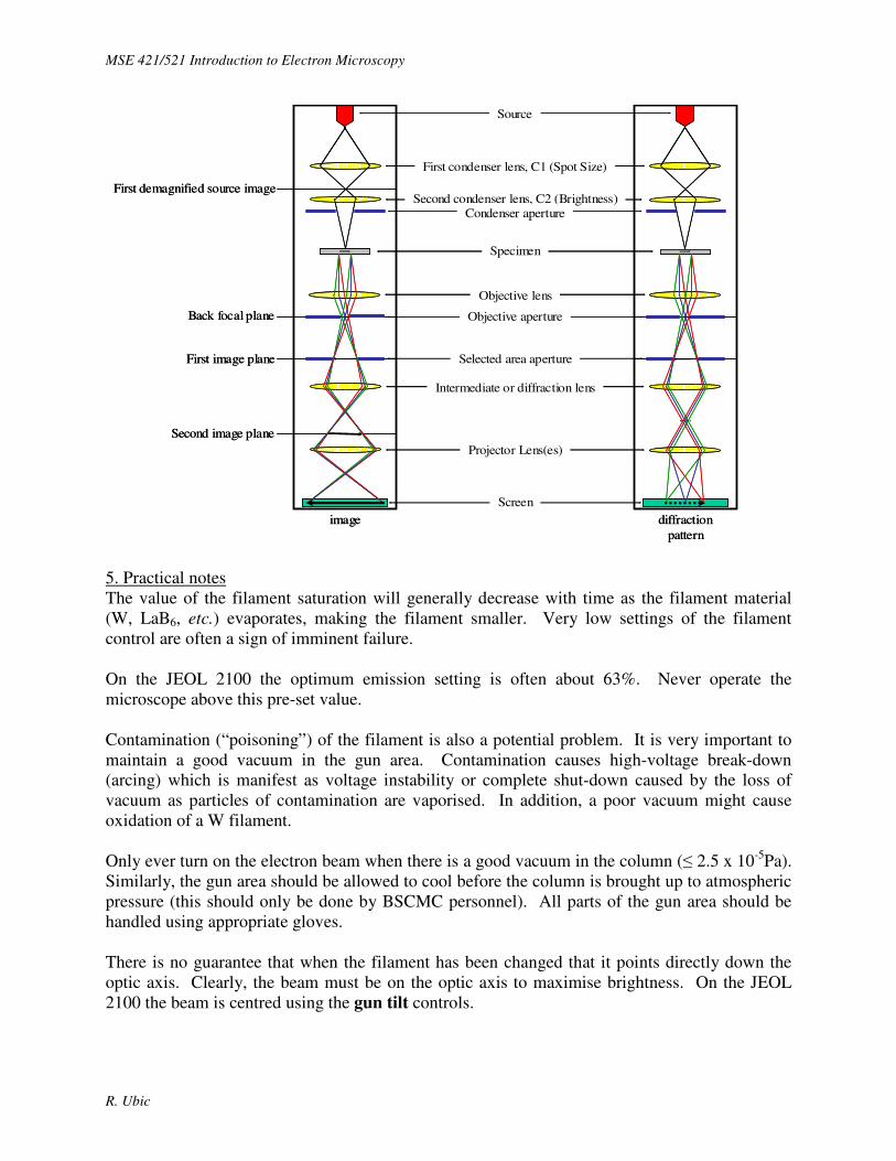
These pumps usually require a rough (backing) pump, although in theory they can operate (slowly) from atmosphere, increasing speed as the pressure is lowered. An ultimate vacuum pressure of 10-5 Pa is achievable. Rotary, diffusion, and turbo pumps are all exhaust pumps - they pull in air from one end and expel it from the other. d. Ion Pump/Ion Getter Pump/Sputter Ion Pump Like diffusion pumps, ion pumps have no moving parts. Unlike diffusion pumps, ion pumps contain no oil, so contamination of the column is not an issue. They rely instead on the ionisation process to remove air.
The sputter ion pump works by ionizing gas that falls within a magnetically confined cold cathode, then reacting these with (or burying them in) plates of titanium. The ion pump consists of two parallel plates (3) of negatively-charged titanium (cathode) and cylindrical anodes (4) all surrounded by large permanent magnets (1). A 5kV potential difference is maintained between the cathode and anode. The titanium cathode emits electrons, which spiral in the magnetic field and ionise air molecules, which are then attracted to the cathode. As titanium is a very reactive metal, most species will simply form a compound with a conveniently low vapour pressure, effectively removing them from the pumped volume. The non-reactive species (e.g., Ar) will tend to simply get embedded in the Ti until the power is removed. In addition, like tiny meteorites, these energetic ions sputter Ti atoms from the surface of the cathode, which mainly condense on the anode, trapping more gas atoms by chemisorption. In this way, Ti acts as a getter material. The smaller the ionic current between electrodes, the lower the vacuum; so the pump acts as its own vacuum gauge. A typical ion pump will actually start to function around 10-3 Pa or so, but this is really abusive. Better practice requires that the chamber already be pumped down with a diffusion pump to about 10-4 Pa. Ultimate vacuum pressures as low as 10-10 Pa are possible in a TEM; but for SEM work (open vacuum system, rubber seals, students abusing them), 10-5 to 10-7

MSE 421/521 Introduction to Electron Microscopy
R. Ubic
Pa is more common. It is common to add ion pumps directly to the stage or gun chamber of a TEM to concentrate their pumping action on these important parts. e. Cryogenic/Adsorption Pumps Cryogenic pumps are also oil-free and rely on liquid nitrogen to cool molecular sieves with large surface areas. The cold surface removed air molecules from ambient pressure down to ~10-4 Pa.
The anticontamination device (ACD) is a cold trap that immediately surrounds the specimen in most TEMs and acts as a minicryopump, trapping volatiles as they are produced from interaction of the beam with the specimen. The ACD provides an alternative site (to your specimen) for condensation of residual contamination in your vacuum. This is an important way to keep the internal components of the TEM clean. Once the beam is off and the trap warms up the trapped gasses are released and removed via the normal pumping system. It is important that the sample be removed before this happens. Ion pumps and crypumps are trapping pumps. They keep the air molecules within them and release them when turned off or warmed up, respectively. f. Vacuum Tube Gauge (Pirani Gauge) A Pirani gauge, named for its German inventor, Marcello Pirani, in 1906, uses a platinum wire in a sealed vacuum tube and a second wire in specimen chamber. A voltage of 6-12 V is applied to heat the wires. A heated metal filament suspended in a gas will lose heat to the gas as its molecules collide with the wire, removing heat and accelerating in the process. If the gas pressure is reduced the number of molecules present will fall proportionately and the wire will rise in temperature due to the reduced cooling effect. So, the hotter the wire, the better the vacuum. The vacuum is measured indirectly by the current which flows through the wire. The higher the temperature of the wire, the greater its electrical resistance and the less current will flow. The difference in current flow between the known vacuum in the closed tube and the unknown vacuum in the instrument gives an indication of the vacuum in the chamber. In many systems the wire is maintained at a constant temperature and the current required to achieve this is therefore a measure of the vacuum being studied.
MSE 421/521 Introduction to Electron Microscopy
R. Ubic
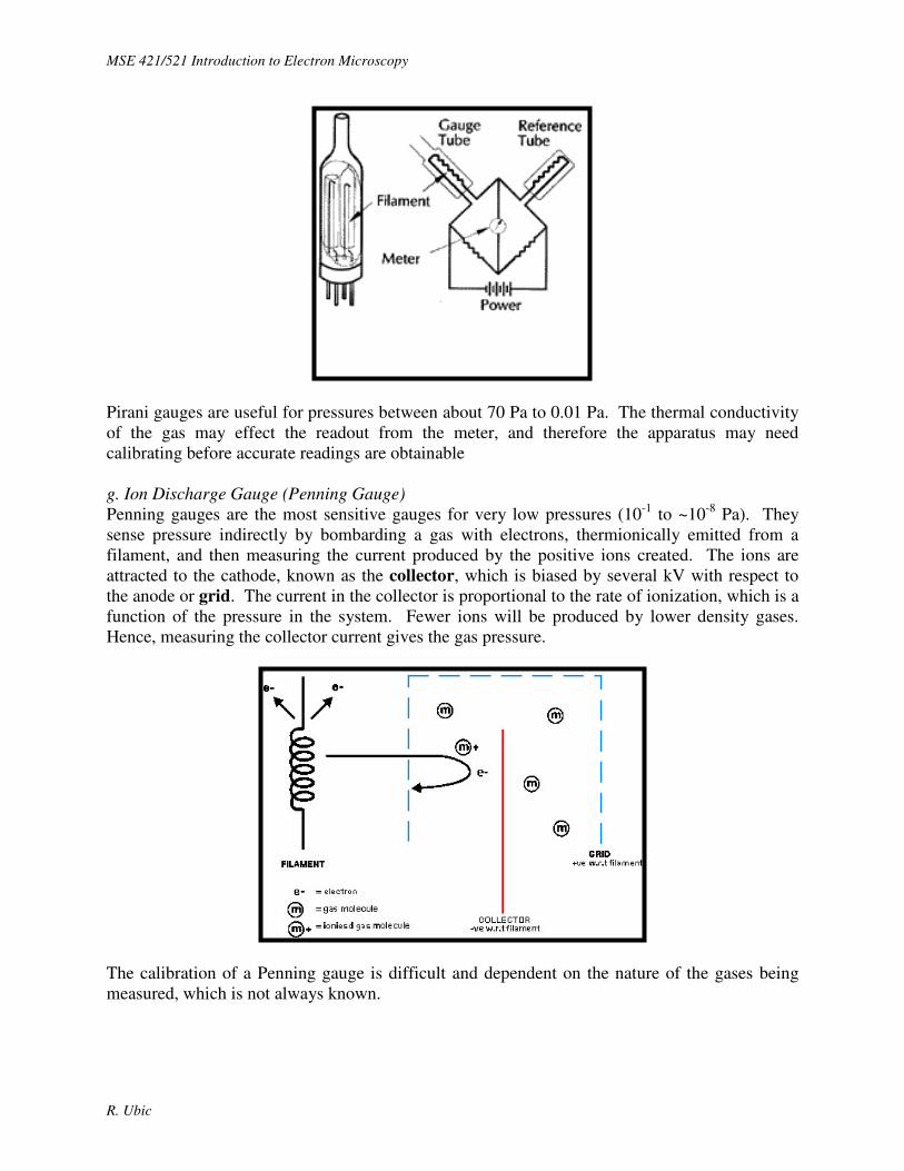
Pirani gauges are useful for pressures between about 70 Pa to 0.01 Pa. The thermal conductivity of the gas may effect the readout from the meter, and therefore the apparatus may need calibrating before accurate readings are obtainable g. Ion Discharge Gauge (Penning Gauge) Penning gauges are the most sensitive gauges for very low pressures (10-1 to ~10-8 Pa). They sense pressure indirectly by bombarding a gas with electrons, thermionically emitted from a filament, and then measuring the current produced by the positive ions created. The ions are attracted to the cathode, known as the collector, which is biased by several kV with respect to the anode or grid. The current in the collector is proportional to the rate of ionization, which is a function of the pressure in the system. Fewer ions will be produced by lower density gases. Hence, measuring the collector current gives the gas pressure.
The calibration of a Penning gauge is difficult and dependent on the nature of the gases being measured, which is not always known.
MSE 421/521 Introduction to Electron Microscopy
R. Ubic
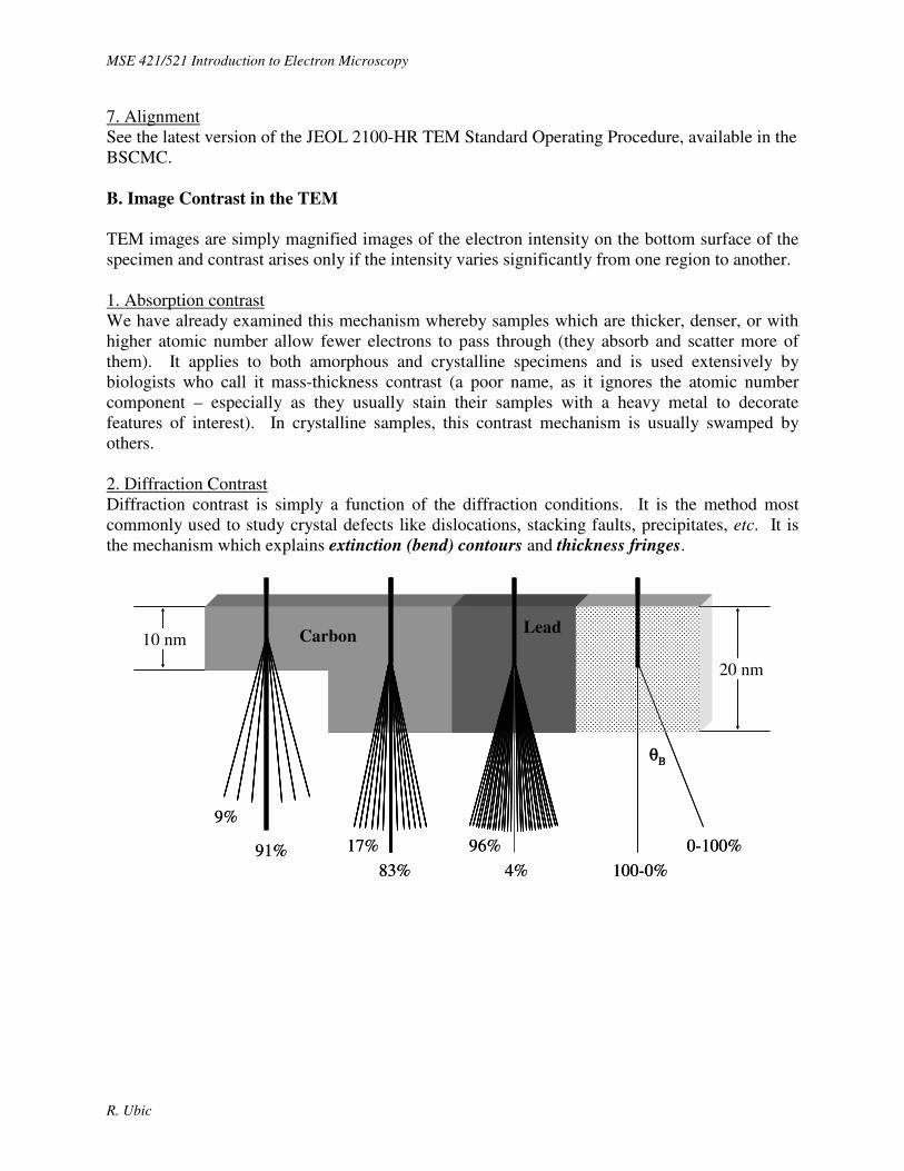
7. Alignment See the latest version of the JEOL 2100-HR TEM Standard Operating Procedure, available in the BSCMC. B. Image Contrast in the TEM TEM images are simply magnified images of the electron intensity on the bottom surface of the specimen and contrast arises only if the intensity varies significantly from one region to another. 1. Absorption contrast We have already examined this mechanism whereby samples which are thicker, denser, or with higher atomic number allow fewer electrons to pass through (they absorb and scatter more of them). It applies to both amorphous and crystalline specimens and is used extensively by biologists who call it mass-thickness contrast (a poor name, as it ignores the atomic number component – especially as they usually stain their samples with a heavy metal to decorate features of interest). In crystalline samples, this contrast mechanism is usually swamped by others. 2. Diffraction Contrast Diffraction contrast is simply a function of the diffraction conditions. It is the method most commonly used to study crystal defects like dislocations, stacking faults, precipitates, etc. It is the mechanism which explains extinction (bend) contours and thickness fringes.
Carbon Lead
9%
91% 17%
83%
96%
4%
θB
0-100%
100-0%
10 nm
20 nm
Carbon Lead
9%
91% 17%
83%
96%
4%
θB
0-100%
100-0%
10 nm
20 nm

MSE 421/521 Introduction to Electron Microscopy
R. Ubic
Objective aperture removesscattered off-axis beams
Sample
ObjectiveAperture
Objective aperture removesdiffracted beams
Electron Beam
Objective aperture removesscattered off-axis beams
SampleSample
ObjectiveApertureObjectiveAperture
Objective aperture removesdiffracted beams
Electron BeamElectron Beam
a. Perfect crystals If a beam of electrons is incident upon a crystal of thickness t, the diffracted intensity for a given reflection can be calculated as:
( )2
πξ
πsinπ
=
s
tsI
gg
where s is the deviation parameter (the deviation of the g vector from the Ewald sphere, or the distance in reciprocal space from the exact Bragg condition) and ξg is a material constant (for a given g) called the extinction distance. Although the maximum diffracted intensity will always be for s = 0, some diffraction will also occur for s ≠ 0. The thinner a crystal is, the further it can deviate from the Bragg condition and still diffract. This rule (which is also true for other forms of diffraction, eg. XRD) can be thought of with reference to the shape and size of the rel rods (II.C.7.) in reciprocal space and their intersections with the Ewald sphere, which we have already discussed. As the crystal thickness increases, the rel rods become shorter and so make fewer intersections with the Ewald sphere – there are fewer reflections in such diffraction patterns. Absorption and increased inelastic scattering also means such patterns show more diffuse scattering and eventually, when the thickness is too great, no intensity at all gets through. The extinction distance is given by:
g
c
F
V
λ
cosθπξ B
g =
where Vc is the volume of the unit cell, θB is the Bragg angle, λ is the electron wavelength, and Fg is the structure factor. The amount of contrast in a specimen, the apparent size of a defect, the

MSE 421/521 Introduction to Electron Microscopy
R. Ubic
appearance of stacking fault fringes, thickness fringes, and bend contours are all determined by ξg. In general, sharp images are only obtained when ξg is small (a few tens of nm). According to the equation above, in order to minimise ξg, θB must be made small and Fg large. These two conditions are only satisfied for low-index reflections. A plot of Ig versus s is called a rocking curve, since variation in s can be achieved by rocking a flat specimen through the Bragg condition. Such a rocking curve is shown below. The yellow curve represents the equation as given above, which is only valid for very thin crystals where the intensity of diffracted beams is negligible (kinematical conditions). The orange curve allows for dynamical effects, and the red curve allows for both dynamical effects and absorption.
Deviation Parameter (nm-1)-0.04 -0.02 0 0.02 0.04
Inte
nsity
of D
iffra
cted
Bea
m
t/ξg = 1.5ξg/ξg’ = 0.1ξg/ξo’ = 0.1
Deviation Parameter (nm-1)-0.04 -0.02 0 0.02 0.04
Inte
nsity
of D
iffra
cted
Bea
m
t/ξg = 1.5ξg/ξg’ = 0.1ξg/ξo’ = 0.1
A buckled specimen provides a range of s values without the need for rocking and so produces fringes just like a rocking curve. The bend or extinction contours which result often reflect the symmetry of the crystal and, in fact, have been used in the past to orient crystals.
Bend contours can easily be distinguished from actual crystalline defects by tilting the specimen. Bend contours will seem to sweep across the specimen as it is tilted and different
Dark-field bend contours in Pb3Nb2O8.

MSE 421/521 Introduction to Electron Microscopy
R. Ubic
planes are brought into the Bragg condition. Actual defects will not appear to move like this, although their appearance will change as the specimen is tilted. From the equation for Ig above, it can be shown that Ig varies periodically with t, becoming zero each time ts is an integer. A typical wedge-shaped specimen shows thickness fringes. The figure below demonstrates this effect. The yellow curve represents the kinematical theory, which predicts that intensity simply rises with thickness. The orange curve represents the more realistic dynamical case, and the red curve shows the additional effect of absorption.
0 100 200 300 400
Thickness (nm)
Inte
nsity
of D
iffra
cted
Bea
m
ξg
ξg = 100 nmξg/ξg’ = 0.1ξg/ξo = 0.1w = 0 (s = 0)
0 100 200 300 400
Thickness (nm)
Inte
nsity
of D
iffra
cted
Bea
m
ξg
ξg = 100 nmξg/ξg’ = 0.1ξg/ξo = 0.1w = 0 (s = 0)
If a crystalline specimen is thicker than about one third the extinction distance, then there will be appreciable interaction between the electron beams as they travel through it. Such interaction renders the kinematical theory inadequate and a dynamical theory is needed. The most straightforward form of this theory only considers interactions between the transmitted beam and one diffracted beam defined by the reciprocal lattice vector g. The Howie-Whelan equations

MSE 421/521 Introduction to Electron Microscopy
R. Ubic
can be used to describe the amplitude of both the diffracted (φg) and undiffracted (φo) beams as a function of z, the distance through the crystal:
( )
( ) gg
gg
iisz
i
dz
d
iszii
dz
d
φξ
ππ2expφ
ξ
πφ
π2expφξ
πφ
ξ
πφ
oo
o
oo
o
+−=
+=
The first term arises from the scattering from the transmitted beam and the second from the diffracted beam. The amplitude of each wave changes with z due to contributions from the other. The possibility of absorption (high-angle inelastic scattering) can be accounted for by replacing 1/ξ with the complex parameter 1/ξ + i/ξ'. In order to calculate the intensity, the equations must be integrated over the entire thickness to give φo and φg at the exit surface of the specimen. The bright-field intensity is then given by
*ooφφ and the dark-field intensity by *φφ gg , where * indicates the complex conjugate. The
intensity of the diffracted beam is then:
( )2
'πξ'πsinπ
=
s
tsI
gg
which is exactly the same as the kinematical solution except for the use of the effective deviation parameter, s', where:
2
2 1'
+=
g
ssξ
b. Defects A defect which disturbs the crystal planes will locally modify the deviation parameter. In this case, the Howie-Whelan equations can be re-written as:
( )
( ) gg
gg
iszi
i
dz
d
sziii
dz
d
φξ
π(π2expφ
ξ
πφ
(π2expφξ
πφ
ξ
πφ
oo
o
oo
o
+•+−=
•++=
Rg
Rg
where R is the displacement of atoms from their lattice positions due to the defect (eg., a Burgers vector), and Rg • modifies the product sz. When Rg • = 0 (or an integer), the defect has no effect on the diffracting planes and so it is invisible. This condition is called the invisibility criterion, and occurs when g is perpendicular to R. Stacking faults, grain boundaries, and phase

MSE 421/521 Introduction to Electron Microscopy
R. Ubic
boundaries can all be studied in this way. The larger Rg • is, the more obviously visible will be the defect. Stacking faults will result in defect fringes which are identical in contrast in both bright-field and dark-field images above the fault but complementary below it. If one grain oriented in a two-beam condition overlaps another which is not, then the first grain can show thickness fringes just as if it were a tapered single crystal (which it is). Such fringes will be parallel to the intersection of the grain boundary with the surface and can easily be distinguished from stacking fault fringes by dark-field imaging, in which case only the strongly diffracting grain will appear bright. When both crystals are strongly diffracting, moiré fringes may appear. These are common in images of thin crystalline materials deposited on each other, where two crystals are diffracting with slightly different values of g or are rotated slightly with respect to each other.
+ =
d1 d2 Dp
d1 d1
+ =Dr
ParallelMoiré Pattern
RotationMoiré Pattern
+ =
d1d1 d2d2 Dp
d1d1 d1d1
+ =Dr
ParallelMoiré Pattern
RotationMoiré Pattern
In the case of parallel lattices, the net effect is a set of fringes running perpendicular to g with a spacing:
21
21
dd
ddD p
−=
and in the case of lattices only rotated by an angle α, the spacing is:
( )α21
1
sin2
dDr =

MSE 421/521 Introduction to Electron Microscopy
R. Ubic
In general, lattices could be rotated and have different spacings, in which case:
αcos2 2122
21
21
dddd
ddD
−+=
Contrast can also arise from dislocations. Planes around the dislocation core are usually distorted quite severely, so if a crystal is oriented into a two-beam condition with s ≠ 0, the planes on one side of the core will be bent through s = 0 and so strongly diffract. If two imaging conditions can be found for which the dislocation is invisible ( 0=• bg ), then b can be
determined by taking the cross product 21 ggb ×= . For edge or mixed dislocations, this condition is slightly less straightforward. The analysis for partial dislocations is also somewhat more complicated.
c. Bright Field and Dark Field Imaging Typically, to simplify TEM analysis we require only one set of planes at the Bragg condition so that there is only one set of reflecting planes. To achieve this it is necessary to orient the sample in such a way that only a single diffraction spot is excited. This reflection, together with the transmitted beam (which is the un-diffracted intensity and is always present in diffraction patterns) gives us what is called a two-beam condition.
1 Å1 Å
Dislocations in nickel
MSE 421/521 Introduction to Electron Microscopy
R. Ubic
g = 002g = 113
g = 111
g = 220
B = [110]
g = 002g = 113g = 113g = 113
g = 111g = 111
g = 220g = 220
B = [110]
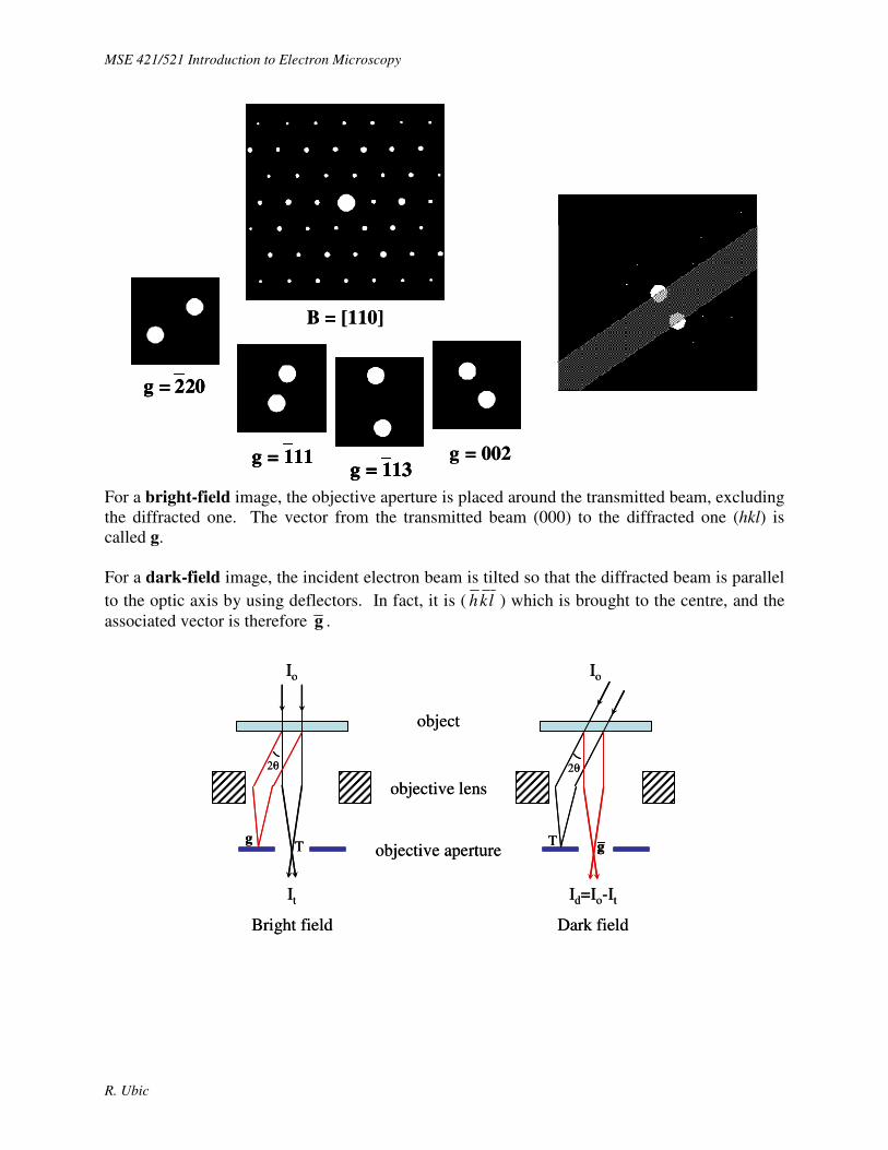
For a bright-field image, the objective aperture is placed around the transmitted beam, excluding the diffracted one. The vector from the transmitted beam (000) to the diffracted one (hkl) is called g. For a dark-field image, the incident electron beam is tilted so that the diffracted beam is parallel to the optic axis by using deflectors. In fact, it is ( lkh ) which is brought to the centre, and the associated vector is therefore g .
Io
object
objective lens
objective aperture
It
Io
Id=Io-It
2θ 2θ
ggT T
Bright field Dark field
Io
object
objective lens
objective aperture
It
Io
Id=Io-It
2θ 2θ
gggT T
Bright field Dark field

MSE 421/521 Introduction to Electron Microscopy
R. Ubic
[101]
vg 440=
[110]
404=
(111) layering visible(111) layering visible
[101]
440=440=
[110]
404=
(111) layering visible(111) layering visible(111) layering visible(111) layering visible
200 nm 200 nm
[101]
440=440=
[110]
404=
(111) layering visible(111) layering visible(111) layering visible(111) layering visible
[101]
440=vg 440=
[110]
404=
(111) layering visible(111) layering visible(111) layering visible(111) layering visible
200 nm 200 nm
vg
[101]
vg 440=vg 440=
[110]
404=
(111) layering visible(111) layering visible(111) layering visible(111) layering visible
[101]
440=440=
[110]
404=
(111) layering visible(111) layering visible(111) layering visible(111) layering visible
200 nm200 nm 200 nm200 nm
[101]
440=440=
[110]
404=
(111) layering visible(111) layering visible(111) layering visible(111) layering visible
[101]
440=vgvg 440=
[110]
404=
(111) layering visible(111) layering visible(111) layering visible(111) layering visible
200 nm200 nm 200 nm200 nm
vgvg
Bright Field
[101]
[110]
440= 404=
200 nm 200 nm
(111) layering visible(111) layering visible
[101]
[110]
440= 404=
200 nm 200 nm
(111) layering visible(111) layering visible(111) layering visible(111) layering visible
[101]
[110]
440= 404=
200 nm200 nm 200 nm200 nm
(111) layering visible(111) layering visible(111) layering visible(111) layering visible
[101]
[110]
440= 404=
200 nm200 nm 200 nm200 nm
(111) layering visible(111) layering visible(111) layering visible(111) layering visible
vg
vg
[101]
[110]
440= 404=
200 nm200 nm 200 nm200 nm
(111) layering visible(111) layering visible(111) layering visible(111) layering visible
[101]
[110]
440= 404=
200 nm200 nm 200 nm200 nm
(111) layering visible(111) layering visible(111) layering visible(111) layering visible
[101]
[110]
440= 404=
200 nm200 nm 200 nm200 nm
(111) layering visible(111) layering visible(111) layering visible(111) layering visible
[101]
[110]
440= 404=
200 nm200 nm 200 nm200 nm
(111) layering visible(111) layering visible(111) layering visible(111) layering visible
vgvg
vgvg
Dark Field
3. Phase contrast and high-resolution imaging Unlike absorption and diffraction contrast mechanisms, which rely on the amplitude of scattered waves, phase contrast results whenever electrons of a different phase pass through the objective aperture. If spots along a systematic row are allowed through, a lattice image is formed. Such images can be used to show the extent of crystallisation of a grain-boundary film or the habit plane of planar defects. If more diffracted beams are allowed to contribute, then a structure
image can be formed. Interpreting such images is not trivial and requires knowledge of specimen thickness, defocus, and TEM resolution (itself dependent on Cs of the objective lens

MSE 421/521 Introduction to Electron Microscopy
R. Ubic
and wavelength). To fully understand high-resolution structural images, a series of images must be obtained and compared to a simulated series of images generated by inputting the likely crystal structure into a sophisticated software package. How many of you were told, perhaps during your first science lessons at school, that atoms are too small to see? Indeed, with typical diameters of 10-10 m, atoms were for a long time considered articles of faith by many scientists. We cannot see atoms, we are later taught, because diffraction places a fundamental limit on the resolution of an image. Roughly speaking, we cannot see anything smaller than the wavelength of the light used to produce the image, and since the wavelength of visible light is some 10,000 times larger than the typical distance between two atoms, we cannot see individual atoms; however, other forms of electromagnetic radiation have much shorter wavelengths than visible light. The x-rays used in crystallography, for example, have wavelengths of less than a nanometre. The problem is that it is extremely difficult to focus x-rays. Luckily, quantum mechanics provides an alternative way to view the microscopic world: subatomic particles like electrons. In diffraction (amplitude) contrast imaging, in general, only one beam is used to form the image (i.e., the transmitted beam in BF or a diffracted beam in DF) so that any phase relationship between the beams is lost. If the transmitted and diffracted beams can be made to recombine (thus preserving their amplitudes and phases) a periodic fringe pattern (lattice image) of the diffracting planes is formed by phase interference between the two beams. This technique usually requires a large objective aperture.
111
000
111111
000
10 nm10 nm
In order to resolve atoms, it is necessary to have the smallest possible objective lens focal length and aberration coefficients. If the diffracted spots from several systematic rows at a zone axis are included in the objective aperture and used to form the image, a structure image of individual rows of atoms may be resolved. The principle in this case is the same that of the Abbe theory for gratings in optics.

MSE 421/521 Introduction to Electron Microscopy
R. Ubic
111111111
[001]
50 Å
[111] [112]
[112]
[110]
[001]
50 Å50 Å
[111] [112]
[112]
[110]
Pb1.5Nb2O6.5. Defocus = -80nm, thickness = 3nm.
50 Å50 Å50 Å
Overlapping <101> SADPs of Sr2Ta2O7 showing (020) spacings (d = 13.599 Å) of two twin variants sharing a common (151) habit plane.
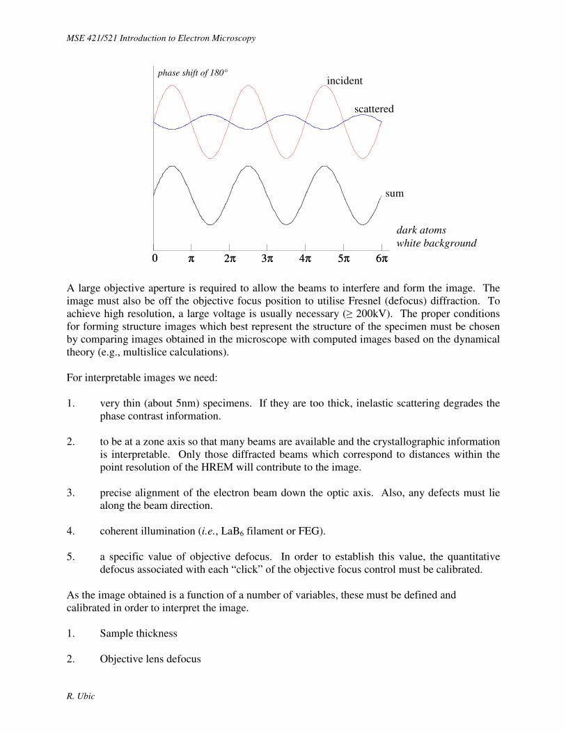
Both high-resolution lattice and structural imaging are examples of phase imaging. Considering the case of just two beams to form the image, in order for the effect of recombining two out-of-phase waves to be visible in the high-resolution electron micrograph (HREM), the amplitudes of the resultant wave (sum of transmitted and diffracted beams) must be different to that of the transmitted beam. The transmitted beam will have a much stronger intensity and so constitutes the background of the image. The greatest change in amplitude (and therefore the greatest contrast in the image) corresponds to the case where the two beams are perfectly in phase. The result is atoms which appear white on a black background. A 90° phase shift causes no change in intensity and therefore no contrast. A 180° phase shift results in a sum wave which is lower in amplitude than the transmitted wave, yielding black atoms on a white background. The microscope introduces some additional phase shifts which complicate this simplistic picture.

MSE 421/521 Introduction to Electron Microscopy
R. Ubic
phase difference of 0°
π 2π 3π 4π 5π 6π0
sum
incident
scattered
phase difference of 0°
π 2π 3π 4π 5π 6π0
sum
incident
scattered
phase shift of 90°
π 2π 3π 4π 5π 6π0
sum
incident
scattered
phase shift of 90°
π 2π 3π 4π 5π 6π0
sum
incident
scattered
white atoms dark background
no contrast
MSE 421/521 Introduction to Electron Microscopy
R. Ubic
phase shift of 180°
π 2π 3π 4π 5π 6π0
sum
incident
scattered
phase shift of 180°
π 2π 3π 4π 5π 6π0
sum
incident
scattered
A large objective aperture is required to allow the beams to interfere and form the image. The image must also be off the objective focus position to utilise Fresnel (defocus) diffraction. To achieve high resolution, a large voltage is usually necessary (≥ 200kV). The proper conditions for forming structure images which best represent the structure of the specimen must be chosen by comparing images obtained in the microscope with computed images based on the dynamical theory (e.g., multislice calculations). For interpretable images we need: 1. very thin (about 5nm) specimens. If they are too thick, inelastic scattering degrades the
phase contrast information. 2. to be at a zone axis so that many beams are available and the crystallographic information
is interpretable. Only those diffracted beams which correspond to distances within the point resolution of the HREM will contribute to the image.
3. precise alignment of the electron beam down the optic axis. Also, any defects must lie
along the beam direction. 4. coherent illumination (i.e., LaB6 filament or FEG). 5. a specific value of objective defocus. In order to establish this value, the quantitative
defocus associated with each “click” of the objective focus control must be calibrated. As the image obtained is a function of a number of variables, these must be defined and calibrated in order to interpret the image. 1. Sample thickness 2. Objective lens defocus
dark atoms white background

MSE 421/521 Introduction to Electron Microscopy
R. Ubic
3. Microscope parameters like kV, Cs, Cc, etc. 4. Number and type of beams included in the objective aperture. 5. Beam tilt Interpreting images of regions inevitably of varying thickness and at different values of defocus is complex because the objective lens is imperfect and itself introduces phase shifts into high-angle information. This problem is formally expressed in terms of the contrast transfer function (CTF) of the objective lens, which is effectively a map of the phase shift including the microscope effects. It gives a measure of the atom contrast (+1 = bright, 0 = invisible, -1 = dark) as a function of atom spacing, but a detailed description of the CTF is beyond the scope of this class. 4. Sample Preparation Preparing samples for use in the TEM is not a trivial exercise. In order to be inserted into the microscope, the sample must be a 3mm-diameter disk thin enough to be electron-transparent. a. Inorganic samples The most common way of preparing electrically conductive materials like metals is electropolishing or jet polishing. The principle of this method is that the specimen is made the anode in an electrolytic cell. When a small voltage is applied, metal is dissolved from the anode and deposited on the cathode. The thin specimen becomes both thinner and smoother, and eventually a hole appears in the sample. The regions around the hole should be thin enough for viewing in the TEM. Automated electropolishers produce 3mm disk samples consisting of relatively thick rims supporting the thin central region. Such samples made in this way are often called foils. Ceramic samples can be prepared in a number of ways; although, as they are non-conductive, electropolishing is not one of them. Starting from a bulk material, an arbitrarily thin slice can be cut away with a diamond wafering blade. Once a thin piece is obtained, one side is polished and glued to a glass slide. The exposed side is then ground down with SiC paper until it is ≈ 100µm thick. Next, a 3mm disk can be ultrasonically machined from it using an ultrasonic drill and some ceramic abrasive powder. This disk will then have to be dimpled, which involves using polishing paste on a rotating wheel to gently wear a bowl-shaped recess into one side of the disk. This process reduces the thickness of the sample and makes it ready for the final – and slowest – part of the procedure: ion beam milling. If a beam of energetic ions is directed at a solid, atoms can be knocked out of the solid in the process known as sputtering. The ion guns commonly used in ion beam thinners generate a plasma by stripping electrons from low-pressure argon atoms in a high electric field. The electric field also accelerates the ions through an aperture in the cathode, producing a beam which is directed onto the TEM sample. Two guns are usually used so that the sample can be thinned from both sides simultaneously, and the sample is rotated to prevent surface roughness from developing. Again, eventually a hole will appear in the sample, and the region around this hole should be thin enough for examination in the TEM.
MSE 421/521 Introduction to Electron Microscopy
R. Ubic
If no ultrasonic drill is available (or if time is short), it is possible to thin the sample by hand to the point where it starts to fall apart. Once the sample starts to fall apart or wear unevenly, it is polished gently. A 3mm support ring (usually copper) is glued to the surface, and the sample is floated off the glass slide by applying heat. The sample is typically so delicate by this point that the excess around the copper ring can simply be broken off, and the ceramic-copper assembly can be placed in the ion beam thinner with or without dimpling. b. Organic samples The preparation of organic materials for the TEM is very complex and typically involves the use of several very toxic materials. The method starts by fixing the sample by soaking it for 30mins to two hours in chemicals like paraformaldehyde, glutaraldehyde, and CaCl in cacodylate buffer. The sample is then washed for 30 - 60 mins in a CaCl-containing cacodylate solution and postfixed for one - two hours in osmium tetroxide. Potassium ferricyanide can also be added for glycogen and stronger stained lipid membranes. The sample is then washed with distilled water, treated in the dark for one - two hours with aqueous uranyl acetate, and washed again, at which stage the sample is finally fixed. The next step is to dehydrate the sample. In order to minimise lipid loss and shrinkage, dehydration is done in stages by soaking the sample in solutions of either ethanol or acetone of increasing concentration (10 - 20 mins soak in 70% ethanol followed by 10 - 20 mins soak in 90% ethanol followed by 15 - 30 mins soak in 100% ethanol). Afterwards, a five-minute soak in a 1:1 mixture of ethanol and propylene oxide followed by a 10-minute soak in pure propylene oxide will complete the dehydration process. The fixed and dehydrated sample is then ready to be embedded in epoxy, usually consisting of a polymer resin (e.g., araldite CY212), hardener like dodecenylsuccinic anhydride (DDSA), plus an accelerator like benzyldimethylamine (BDMA). Over the course of the next few days, the sample is embedded with this resin in a suitable mould and left in an oven at 60°C for 48 hours to complete the polymerisation. Once complete, thin slices can be sliced off the embedded sample with a microtome, which is an apparatus used to cut thin sections of a specimen with a knife that is made of either steel, glass, sapphire, or diamond. The thin sections are then collected onto a copper support grid, coated with carbon if necessary, and examined in the TEM.