Embed Size (px)
DESCRIPTION
KYOCERA MITA PointSource Vi 30 Service Manual
Citation preview
Handling precautionsHandling precautions
SpecificationsSpecifications
Mechanical constructionMechanical construction
Electrical components lay-outElectrical components lay-out
Paper jam detectionPaper jam detection
Circuit board operationCircuit board operation
Set-upSet-up
Service mode and test modeService mode and test mode
Assembly and adjustmentsAssembly and adjustments
Replacing the main circuit boardReplacing the main circuit board
Self diagnosticsSelf diagnostics
Trouble shootingTrouble shooting
Timing charts and circuit diagrams Timing charts and circuit diagrams
Contents pagesContents pages
Manual front coverManual front cover
Parts list - exploded viewsParts list - exploded views
Parts list indexParts list index
PointPointSourceSource Vi 30 Service manual Vi 30 Service manual (including parts lists)(including parts lists)
354
1-1-1
1-1-1 Specifications
Type ............................................... Desktop transceiver/receiverPower source ................................. 120 V AC, 60 Hz, 4.2 A
220 - 240 V AC, 50/60 Hz, 2.1 APower consumption ....................... Rated: 500 W (220 - 240 V AC), 500 W (120 V AC)
In ready mode: 500 W (220 - 240 V AC),500 W (120 V AC)
During receiving: Normal mode 500 W (220 - 240 V AC), 500 W (120 V AC)
In auto shutoff mode: 15 W or less (220 - 240 V AC)15 W or less (120 V AC)
Dimensions .................................... 403 mm (W) × 308 mm (D) × 240 mm (H)157/8" (W) × 121/8" (D) × 97/16" (H)
Weight ............................................ Approx. 8.72 kg/193/16 IbsOption ............................................ Memory board (1 M bytes, 2 M bytes), Extension
memory (4 M bytes/SIMM)
• Facsimile functionApplicable line ................................ Subscription telephone lineCompatibility .................................. Group 3Communications system ................ Half-duplexModulation ..................................... TCM, QAM, PhMEncoding system ............................ MMR, MH, MRError correction .............................. ITU-T ECMModem speed ................................ 14400/12000/9600/7200/4800/2400/300 bps with
automatic fallbackMinimum transmission rate ............ 10 ms/line (normal mode), 5 ms/line (fine mode)Transmission time .......................... Within 7 s (ITU-T #1 chart, MMR (ECM), memory
transmission)Memory capacity ............................ 256 k bytesResolution mode ............................ Normal mode, Fine mode, Super fine modeGray-scale ...................................... 64 levelsFunctions ....................................... Refer to table 1-1-1 on page 1-1-2

354
1-1-2
Operation features One-touch dialing (10 destinations)
Abbreviated number dialing (50 destinations)
Group dialing (10 destinations)
Auto redialing
Manual redialing
Remote switching
Transmit reservation
Automatic reduction in reception mode
Automatic FAX/TEL switching
D.R.D. (Distinctive ring service) reception (For inch models
only)
Timer controlled transmit function
Polling communications
Memory polling
Reliability features TTI
ECM
Transmit/Receive terminal display
Retransmission for error communication
Reporting features Activity report
Transmission report
Error report
Preset (Setting/registration) list
Power failure report
Memory file report
G3 monitor report
Class 1 report
Memory features Out-of-paper (memory) reception function
Broadcast function (50 destinations)
Dual access
Batch transmission
Memory transfer
Telephone features Pulse tone transmission
TAD reception / Message telephone reception
Table 1-1-1
354
1-1-3
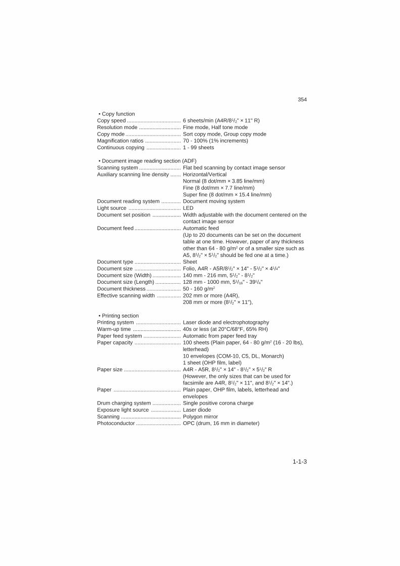
• Copy functionCopy speed .................................... 6 sheets/min (A4R/81/2" × 11" R)Resolution mode ............................ Fine mode, Half tone modeCopy mode ..................................... Sort copy mode, Group copy modeMagnification ratios ........................ 70 - 100% (1% increments)Continuous copying ....................... 1 - 99 sheets
• Document image reading section (ADF)Scanning system ............................ Flat bed scanning by contact image sensorAuxiliary scanning line density ....... Horizontal/Vertical
Normal (8 dot/mm × 3.85 line/mm)Fine (8 dot/mm × 7.7 line/mm)Super fine (8 dot/mm × 15.4 line/mm)
Document reading system ............. Document moving systemLight source ................................... LEDDocument set position ................... Width adjustable with the document centered on the
contact image sensorDocument feed ............................... Automatic feed
(Up to 20 documents can be set on the documenttable at one time. However, paper of any thicknessother than 64 - 80 g/m2 or of a smaller size such asA5, 81/2" × 51/2" should be fed one at a time.)
Document type ............................... SheetDocument size ............................... Folio, A4R - A5R/81/2" × 14" - 51/2" × 41/4"Document size (Width) ................... 140 mm - 216 mm, 51/2" - 81/2"Document size (Length) ................. 128 mm - 1000 mm, 51/16" - 391/4"Document thickness ....................... 50 - 160 g/m2
Effective scanning width ................ 202 mm or more (A4R),208 mm or more (81/2" × 11"),
• Printing sectionPrinting system .............................. Laser diode and electrophotographyWarm-up time ................................ 40s or less (at 20°C/68°F, 65% RH)Paper feed system ......................... Automatic from paper feed trayPaper capacity ............................... 100 sheets (Plain paper, 64 - 80 g/m2 (16 - 20 lbs),
letterhead)10 envelopes (COM-10, C5, DL, Monarch)1 sheet (OHP film, label)
Paper size ...................................... A4R - A5R, 81/2" × 14" - 81/2" × 51/2" R(However, the only sizes that can be used forfacsimile are A4R, 81/2" × 11", and 81/2" × 14".)
Paper ............................................. Plain paper, OHP film, labels, letterhead andenvelopes
Drum charging system ................... Single positive corona chargeExposure light source .................... Laser diodeScanning ........................................ Polygon mirrorPhotoconductor .............................. OPC (drum, 16 mm in diameter)
354
1-1-4
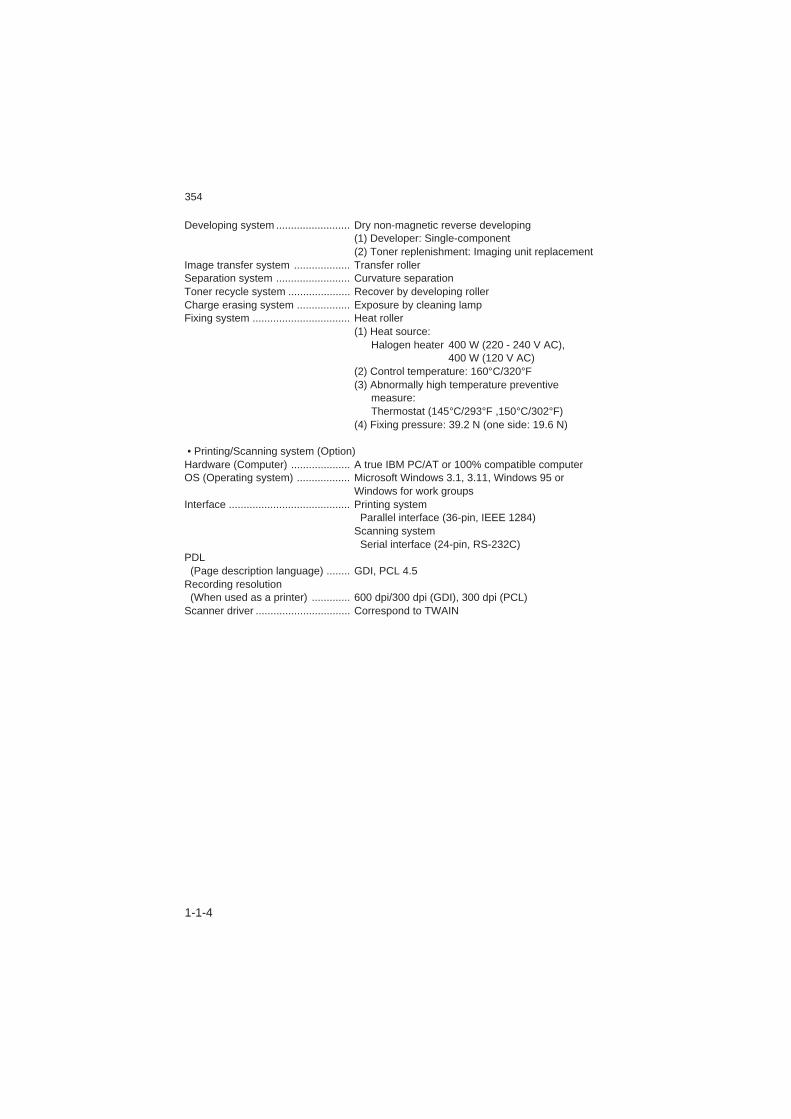
Developing system ......................... Dry non-magnetic reverse developing(1) Developer: Single-component(2) Toner replenishment: Imaging unit replacement
Image transfer system ................... Transfer rollerSeparation system ......................... Curvature separationToner recycle system ..................... Recover by developing rollerCharge erasing system .................. Exposure by cleaning lampFixing system ................................. Heat roller
(1) Heat source:Halogen heater 400 W (220 - 240 V AC),
400 W (120 V AC)(2) Control temperature: 160°C/320°F(3) Abnormally high temperature preventive
measure:Thermostat (145°C/293°F ,150°C/302°F)
(4) Fixing pressure: 39.2 N (one side: 19.6 N)
• Printing/Scanning system (Option)Hardware (Computer) .................... A true IBM PC/AT or 100% compatible computerOS (Operating system) .................. Microsoft Windows 3.1, 3.11, Windows 95 or
Windows for work groupsInterface ......................................... Printing system
Parallel interface (36-pin, IEEE 1284)Scanning system Serial interface (24-pin, RS-232C)
PDL (Page description language) ........ GDI, PCL 4.5Recording resolution (When used as a printer) ............. 600 dpi/300 dpi (GDI), 300 dpi (PCL)Scanner driver ................................ Correspond to TWAIN
354
1-2-1
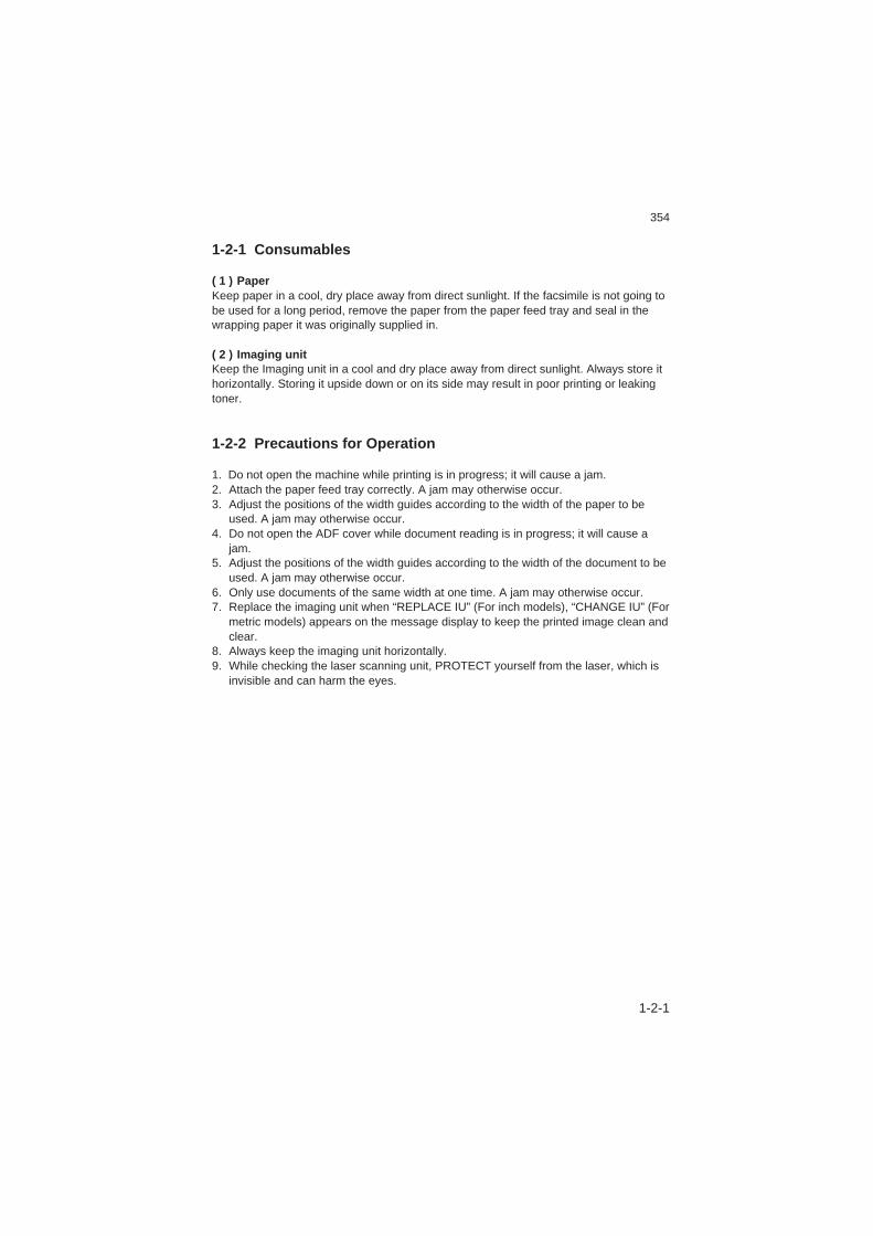
1-2-1 Consumables
( 1 ) PaperKeep paper in a cool, dry place away from direct sunlight. If the facsimile is not going tobe used for a long period, remove the paper from the paper feed tray and seal in thewrapping paper it was originally supplied in.
( 2 ) Imaging unitKeep the Imaging unit in a cool and dry place away from direct sunlight. Always store ithorizontally. Storing it upside down or on its side may result in poor printing or leakingtoner.
1-2-2 Precautions for Operation
1. Do not open the machine while printing is in progress; it will cause a jam.2. Attach the paper feed tray correctly. A jam may otherwise occur.3. Adjust the positions of the width guides according to the width of the paper to be
used. A jam may otherwise occur.4. Do not open the ADF cover while document reading is in progress; it will cause a
jam.5. Adjust the positions of the width guides according to the width of the document to be
used. A jam may otherwise occur.6. Only use documents of the same width at one time. A jam may otherwise occur.7. Replace the imaging unit when “REPLACE IU” (For inch models), “CHANGE IU” (For
metric models) appears on the message display to keep the printed image clean andclear.
8. Always keep the imaging unit horizontally.9. While checking the laser scanning unit, PROTECT yourself from the laser, which is
invisible and can harm the eyes.

354
1-2-2
1-2-3 Document
( 1 ) Types of documentThis machine can use the following types of document • Sizes: Folio, A4R - A5R/81/2" × 14" - 51/2" × 41/4"
(Width: 140 mm - 216 mm, 51/2" - 81/2", Length: 128 mm - 1000 mm, 51/16" - 391/4")(However, documents that are longer than 355 mm/14" must be assisted by handwhile they pass by. Also, the maximum length setting can be changed with memoryswitch No. 51.)
• Thickness: 50 g/m2 - 160 g/m2
• CapacityUp to 20 documents can be set on the document table at one time. (However, paperof any thickness other than 64 - 80 g/m2 or of a smaller size such as A5, 81/2" × 51/2"should be fed one at a time.)
[Precautions] • The area within 4 mm from top or bottom and 10 mm from right or left side of a
document may not be transmitted. • The size of paper printed at destination party may differ from the one which was used
for transmitting. • When an documents longer than the maximum length passes by, this is treated as a
document jam and “DOCUMENT JAM” is displayed in the message display. • Very low density characters may not be printed on the destination facsimile unit. • Do not transmit hand-written or stamped documents until they are completely dry. • Remove clips and staples from documents before transmitting. (After removing the
staples, fan the documents to ensure they do not stick together.) • Documents that do not meet size and thickness requirements may not be transmitted
successfully. • Do not feed different size documents through the ADF simultaneously or jams may
occur. • If some of the document are crinkled, bent or curled, make those flat, and be careful
to insert those documents.
354
1-2-3
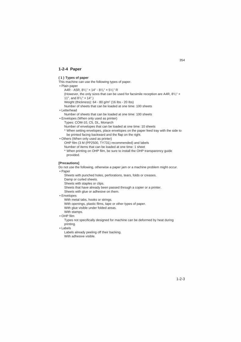
1-2-4 Paper
( 1 ) Types of paperThis machine can use the following types of paper. • Plain paper
A4R - A5R, 81/2" × 14" - 81/2" × 51/2" R(However, the only sizes that can be used for facsimile reception are A4R, 81/2" ×11", and 81/2" × 14".)Weight (thickness): 64 - 80 g/m2 (16 Ibs - 20 Ibs)Number of sheets that can be loaded at one time: 100 sheets
• LetterheadNumber of sheets that can be loaded at one time: 100 sheets
• Envelopes (When only used as printer)Types: COM-10, C5, DL, MonarchNumber of envelopes that can be loaded at one time: 10 sheets* When setting envelopes, place envelopes on the paper feed tray with the side to
be printed facing backward and the flap on the right. • Others (When only used as printer)
OHP film (3 M (PP2500, TY731) recommended) and labelsNumber of items that can be loaded at one time: 1 sheet* When printing on OHP film, be sure to install the OHP transparency guide
provided.
[Precautions]Do not use the following, otherwise a paper jam or a machine problem might occur. • Paper
Sheets with punched holes, perforations, tears, folds or creases.Damp or curled sheets.Sheets with staples or clips.Sheets that have already been passed through a copier or a printer.Sheets with glue or adhesive on them.
• EnvelopesWith metal tabs, hooks or strings.With openings, plastic films, tape or other types of paper.With glue visible under folded areas.With stamps.
• OHP filmTypes not specifically designed for machine can be deformed by heat duringprinting.
• LabelsLabels already peeling off their backing.With adhesive visible.
354
1-3-1
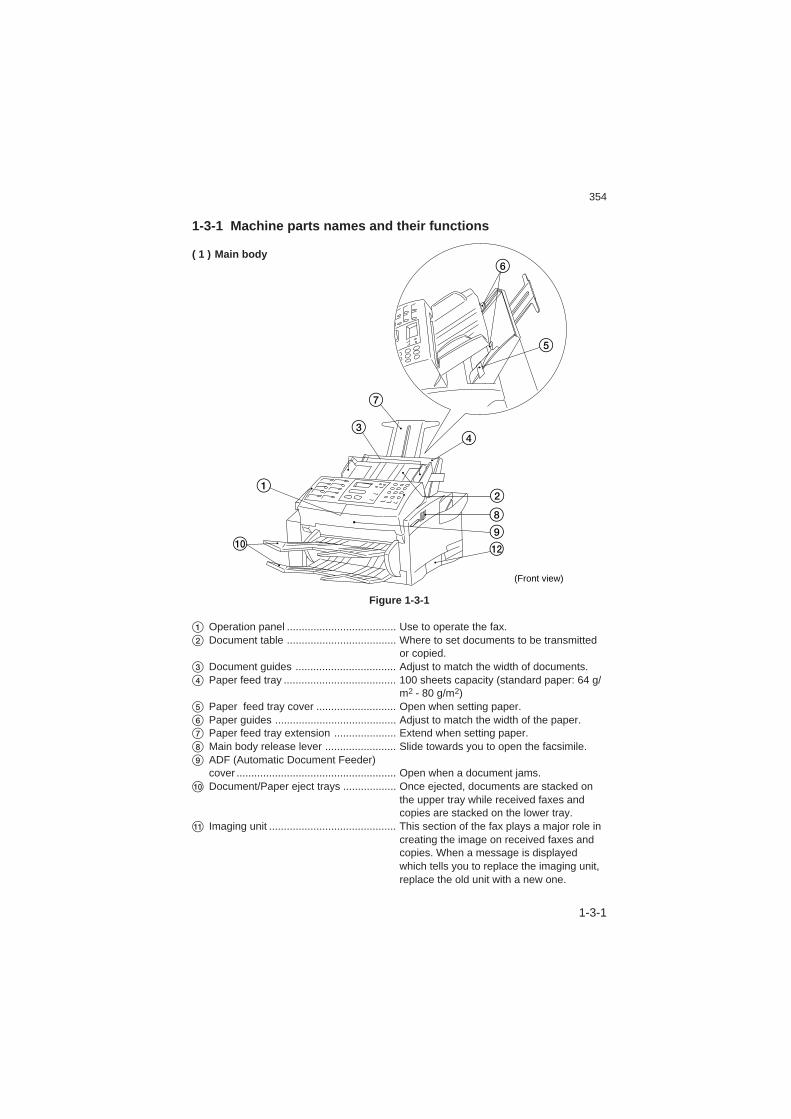
1-3-1 Machine parts names and their functions
( 1 ) Main body
1
3
7
4
8
@
2
09
5
6
(Front view)
Figure 1-3-1
1 Operation panel ..................................... Use to operate the fax.2 Document table ..................................... Where to set documents to be transmitted
or copied.3 Document guides .................................. Adjust to match the width of documents.4 Paper feed tray ...................................... 100 sheets capacity (standard paper: 64 g/
m2 - 80 g/m2)5 Paper feed tray cover ........................... Open when setting paper.6 Paper guides ......................................... Adjust to match the width of the paper.7 Paper feed tray extension ..................... Extend when setting paper.8 Main body release lever ........................ Slide towards you to open the facsimile.9 ADF (Automatic Document Feeder)
cover ...................................................... Open when a document jams.0 Document/Paper eject trays .................. Once ejected, documents are stacked on
the upper tray while received faxes andcopies are stacked on the lower tray.
! Imaging unit ........................................... This section of the fax plays a major role increating the image on received faxes andcopies. When a message is displayedwhich tells you to replace the imaging unit,replace the old unit with a new one.

354
1-3-2
%
(
#
$
^&
)
(Rear view)
*!
(
@
(Internal view)
*1
*1
*1
Figure 1-3-2
@ Fax moving handles .......................... Hold these handles when moving thefacsimile.
# Telephone jack .................................. For connecting the handset (*1) or aseparately purchased telephone.
$ Line jack ............................................ For connecting the fax to a telephone linevia the modular cord.
% Power receptacle .............................. For connecting the power cord.^ Printer connector (Parallel port) ........ For connecting a 36-pin parallel cable.& Printer connector (Serial port) ........... For connecting a 24-pin RS-232C cable.
*1 * Handset ............................................. Use as a standard telephone and whenanswering calls in the manual fax receptionmode.
*1 ( Handset rest ...................................... Place the handset here when not in use.) Paper table release buttons .............. Press when removing the paper table from
the facsimile.
*1: For inch models only
354
1-3-3
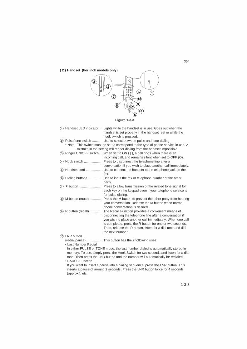
( 2 ) Handset (For inch models only)
P/T
O/I 1 2
5
#0
6
7
ABC DEF
GHI JKL MNO
PRS TUV WXY
OPER
M R LNR
8 9
3
4
16
098
7
32
45
Figure 1-3-3
1 Handset LED indicator ... Lights while the handset is in use. Goes out when thehandset is set properly in the handset rest or while thehook switch is pressed.
2 Pulse/tone switch ........... Use to select between pulse and tone dialing.* Note: This switch must be set to correspond to the type of phone service in use. A
mistake in the setting will render dialing from the handset impossible.3 Ringer ON/OFF switch ... When set to ON ( | ), a bell rings when there is an
incoming call, and remains silent when set to OFF (O).4 Hook switch .................... Press to disconnect the telephone line after a
conversation if you wish to place another call immediately.5 Handset cord .................. Use to connect the handset to the telephone jack on the
fax.6 Dialing buttons ................ Use to input the fax or telephone number of the other
party.7 *button ......................... Press to allow transmission of the related tone signal for
each key on the keypad even if your telephone service isfor pulse dialing.
8 M button (mute) .............. Press the M button to prevent the other party from hearingyour conversation. Release the M button when normalphone conversation is desired.
9 R button (recall) .............. The Recall Function provides a convenient means ofdisconnecting the telephone line after a conversation ifyou wish to place another call immediately. When one callis completed, press the R button for one or two seconds.Then, release the R button, listen for a dial tone and dialthe next number.
0 LNR button(redial/pause) ................. This button has the 2 following uses:• Last Number RedialIn either PULSE or TONE mode, the last number dialed is automatically stored inmemory. To use, simply press the Hook Switch for two seconds and listen for a dialtone. Then press the LNR button and the number will automatically be redialed.
• PAUSE FunctionIf you want to insert a pause into a dialing sequence, press the LNR button. Thisinserts a pause of around 2 seconds. Press the LNR button twice for 4 seconds(approx.), etc.
354
1-3-4
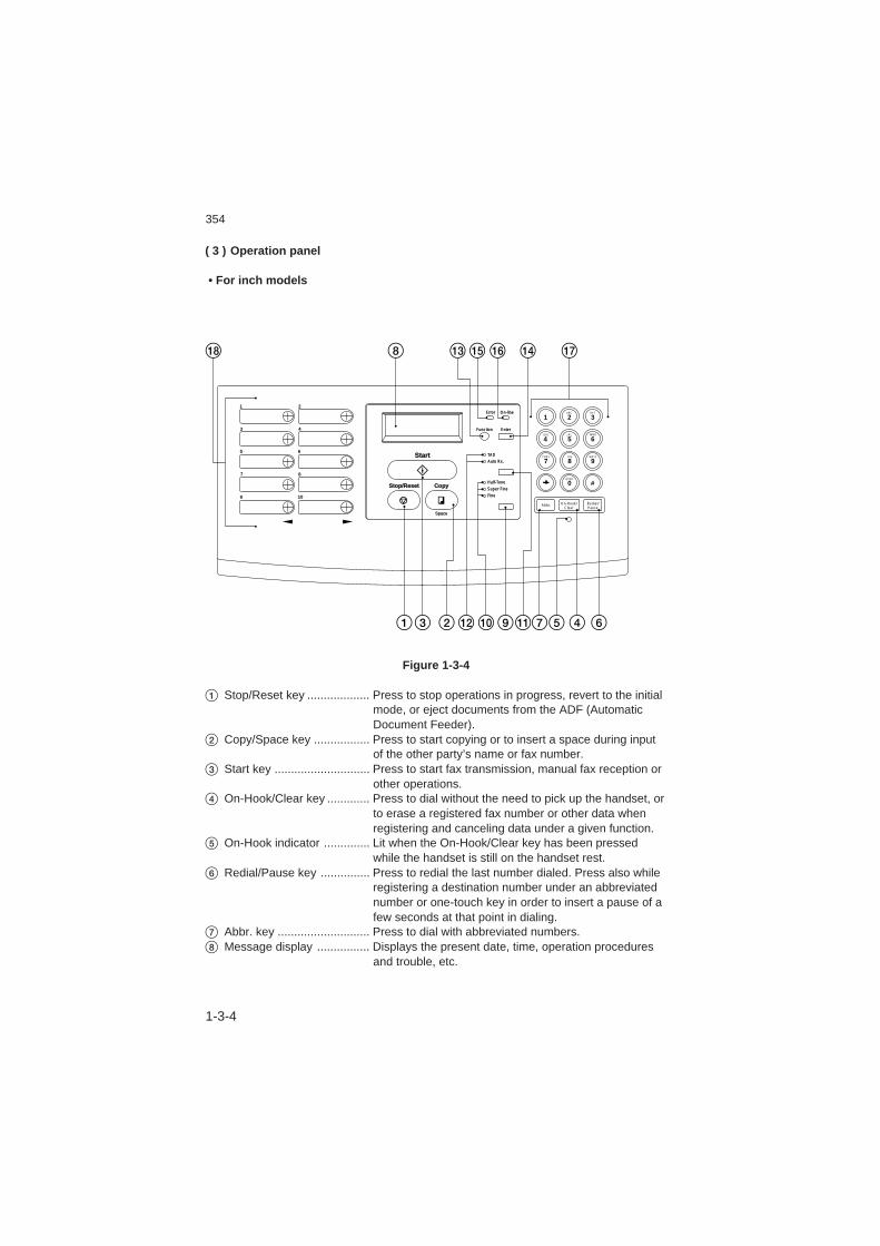
( 3 ) Operation panel
• For inch models
1 2
3 4
5 6
7 8
9 10
TAD
Function Enter
Auto Rx.
Super Fine
Fine
Error On-line
Half-Tone
Space
1 2 3
4 5 6
7 8 9
0 #
ABC DEF
GHI JKL MNO
PQRS TUV WXYZ
Abbr. On-Hook/Clear
Redial/Pause
OPER
&
31 2 4 65
8
9!@0
# $% ^*
7
Start
CopyStop/Reset
Figure 1-3-4
1 Stop/Reset key ................... Press to stop operations in progress, revert to the initialmode, or eject documents from the ADF (AutomaticDocument Feeder).
2 Copy/Space key ................. Press to start copying or to insert a space during inputof the other party’s name or fax number.
3 Start key ............................. Press to start fax transmission, manual fax reception orother operations.
4 On-Hook/Clear key ............. Press to dial without the need to pick up the handset, orto erase a registered fax number or other data whenregistering and canceling data under a given function.
5 On-Hook indicator .............. Lit when the On-Hook/Clear key has been pressedwhile the handset is still on the handset rest.
6 Redial/Pause key ............... Press to redial the last number dialed. Press also whileregistering a destination number under an abbreviatednumber or one-touch key in order to insert a pause of afew seconds at that point in dialing.
7 Abbr. key ............................ Press to dial with abbreviated numbers.8 Message display ................ Displays the present date, time, operation procedures
and trouble, etc.
354
1-3-5
9 Resolution mode select key ............ Press to select the degree of resolution mostsuitable to the documents being transmitted orcopied.
0 Resolution mode indicators ............. The uppermost indicator is for the Half-Tonemode, the middle indicator is for the Super Finemode, and the lowermost indicator is for theFine mode. Press the resolution mode selectkey to light the resolution mode indicatorcorresponding to the desired mode. When all ofthe indicators are out, the fax is in the Normalmode.
! Reception mode select key ............. Press to select the desired reception mode.@ Reception mode indicators .............. The uppermost indicator is the TAD indicator.
The bottom indicator is the Auto Rx. indicator.Press the reception mode select key to light thereception mode indicator corresponding to thedesired mode. When using a separatelypurchased telephone with answering machinecapabilities in conjunction with the fax, makesure the TAD indicator is lit. When using theautomatic fax reception mode, make sure theAuto Rx. indicator is lit. When using the manualfax reception mode with the handset connectedto the facsimile, both indicators should be out.
# Function key .................................... Press to select one of the facsimile’s functionsor registration procedures.
$ Enter key ......................................... Press during registration and settingprocedures to register the currently entereddata under a given function.
% Error indicator .................................. Lit when a communications error or mechanicalproblem has occurred.
^ On-line indicator .............................. Lit when the facsimile is to be used as a printeror scanner.
& Keypad ............................................ Use to dial a fax number, or to input faxnumbers for registration under abbreviatednumbers and one-touch keys.
* Even if your telephone service is for pulse dialing, press the * key afterconnecting to the other party and any key pressed on the keypad after that willtransmit the related tone signal.
* One-touch keys (1 - 10) .................. Press to dial fax numbers registered under thecorresponding one-touch key. Each of the 10keys can be designated to function as either aone-touch key, a group dial or a batchtransmission key.
* When inputting names, etc., press one-touch key No. 9 to move the cursor to theleft, and one-touch key No. 10 to move the cursor to the right.
354
1-3-6
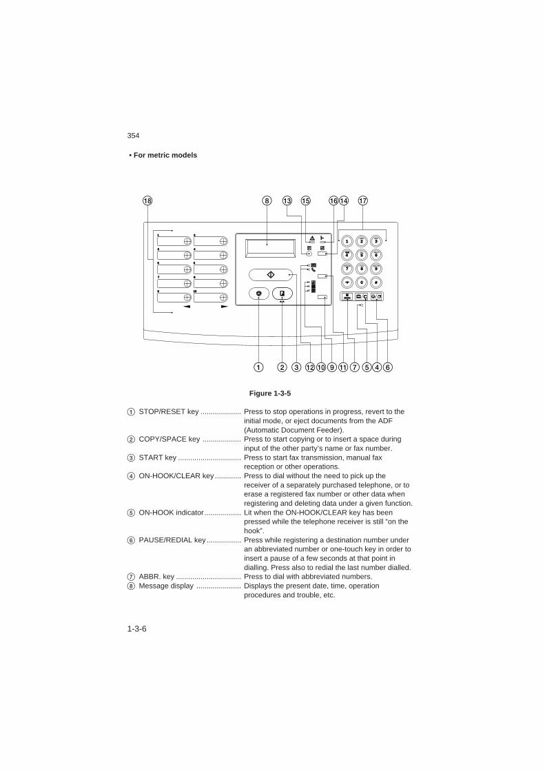
• For metric models
&
1 2 3 465
8
9!@0
# $% ^*
7
1 2
3 4
5 6
7 8
9 10
A A
1 2 3
4 5 6
7 8 9
0 #
C
GHI
ABC DEF
JKL MNO
PQRS TUV WXYZ
Figure 1-3-5
1 STOP/RESET key .................... Press to stop operations in progress, revert to theinitial mode, or eject documents from the ADF(Automatic Document Feeder).
2 COPY/SPACE key ................... Press to start copying or to insert a space duringinput of the other party’s name or fax number.
3 START key ............................... Press to start fax transmission, manual faxreception or other operations.
4 ON-HOOK/CLEAR key ............. Press to dial without the need to pick up thereceiver of a separately purchased telephone, or toerase a registered fax number or other data whenregistering and deleting data under a given function.
5 ON-HOOK indicator .................. Lit when the ON-HOOK/CLEAR key has beenpressed while the telephone receiver is still “on thehook”.
6 PAUSE/REDIAL key ................. Press while registering a destination number underan abbreviated number or one-touch key in order toinsert a pause of a few seconds at that point indialling. Press also to redial the last number dialled.
7 ABBR. key ................................ Press to dial with abbreviated numbers.8 Message display ...................... Displays the present date, time, operation
procedures and trouble, etc.

354
1-3-7
9 Resolution mode select key ..... Press to select the degree of resolution mostsuitable to the documents being transmitted orcopied.
0 Resolution mode indicators ...... The uppermost indicator is for the PHOTO MODEsetting, the middle indicator is for the SUPER FINEmode, and the lowermost indicator is for the FINEmode. Press the resolution mode select key to lightthe resolution mode indicator corresponding to thedesired mode. When all of the indicators are out,the fax is in the NORMAL mode.
! Reception mode select key ...... Press to select the desired reception mode.@ Reception mode indicators ....... The uppermost indicator is the MESSAGE TEL.
indicator. The bottom indicator is the MANUAL RX.indicator. Press the reception mode select key tolight the reception mode indicator corresponding tothe desired mode. When using a separatelypurchased telephone with message telephonecapabilities in conjunction with the fax, make surethe MESSAGE TEL. indicator is lit. When using themanual fax reception mode with a separatelypurchased telephone connected to the facsimile,make sure the MANUAL RX. indicator is lit. Whenusing the automatic fax reception mode, bothindicators should be out.
# FUNCTION key ........................ Press to select one of the facsimile’s functions orregistration procedures.
$ ENTER FUNCTION key ........... Press during registration and setting procedures toregister the currently entered data under a givenfunction.
% ERROR indicator ...................... Lit when a communications error or mechanicalproblem has occurred.
^ ON LINE indicator .................... Lit when the facsimile is to be used as a printer orscanner.
& Keypad ..................................... Use to dial a fax number, or to input fax numbersfor registration under abbreviated numbers andone-touch keys.
* Even if your telephone service is for pulse dialling, press the * key afterconnecting to the other party and any key pressed on the keypad after that willtransmit the related tone signal.
* One-touch keys (1 - 10) ........... Press to dial fax numbers registered under thecorresponding one-touch key. Each of the 10 keyscan be designated to function as either a one-touchkey, a group dial or a batch transmission key.
* When inputting names, etc., press one-touch key No. 9 to move the cursor to theleft, and one-touch key No. 10 to move the cursor to the right.
Note: Available functions may differ depending upon the country and region where this unitwas purchased.
354
1-3-8
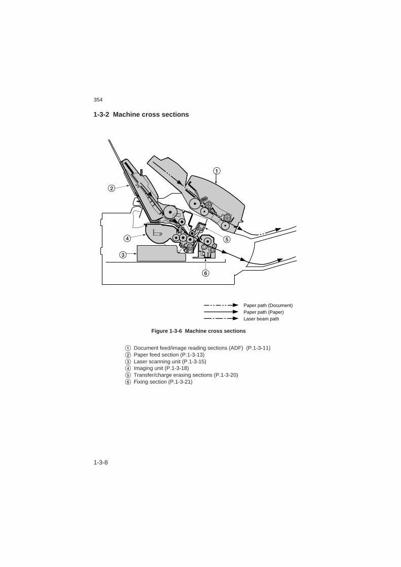
1-3-2 Machine cross sections
1
2
3
4 5
6
Paper path (Document)Paper path (Paper)Laser beam path
Figure 1-3-6 Machine cross sections
1 Document feed/image reading sections (ADF) (P.1-3-11)2 Paper feed section (P.1-3-13)3 Laser scanning unit (P.1-3-15)4 Imaging unit (P.1-3-18)5 Transfer/charge erasing sections (P.1-3-20)6 Fixing section (P.1-3-21)
354
1-3-9
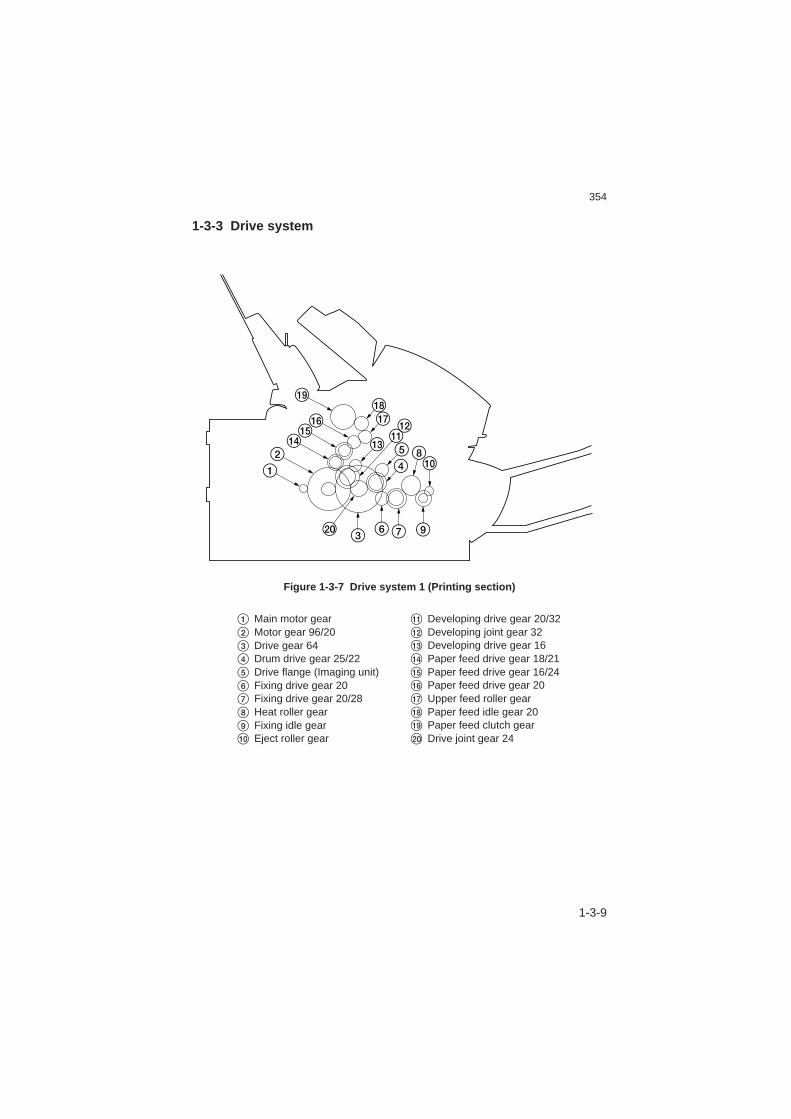
1-3-3 Drive system
12 5
48
9763
0
!@
#$%^
*&
(
)
Figure 1-3-7 Drive system 1 (Printing section)
1 Main motor gear2 Motor gear 96/203 Drive gear 644 Drum drive gear 25/225 Drive flange (Imaging unit)6 Fixing drive gear 207 Fixing drive gear 20/288 Heat roller gear9 Fixing idle gear0 Eject roller gear
! Developing drive gear 20/32@ Developing joint gear 32# Developing drive gear 16$ Paper feed drive gear 18/21% Paper feed drive gear 16/24^ Paper feed drive gear 20& Upper feed roller gear* Paper feed idle gear 20( Paper feed clutch gear) Drive joint gear 24

354
1-3-10
1234
57
68
Figure 1-3-8 Drive system 2 (Document feed section (ADF))
4 38
2
157
6
Figure 1-3-9 Drive system 3 (Imaging unit)
1 ADF motor gear2 Idle gear 16/653 Idle gear 214 Joint gear 37
5 ADF conveying gear 366 Idle gear 16/377 ADF paper feed gear 518 ADF conveying gear 36
1 Developing drive gear 16 (Main body)2 Developing roller gear3 Developing idle gear 204 Idle gear 25/18
5 Sub-roller gear6 Idle gear 307 Agitation gear8 Drive flange (drum)
354
1-3-11
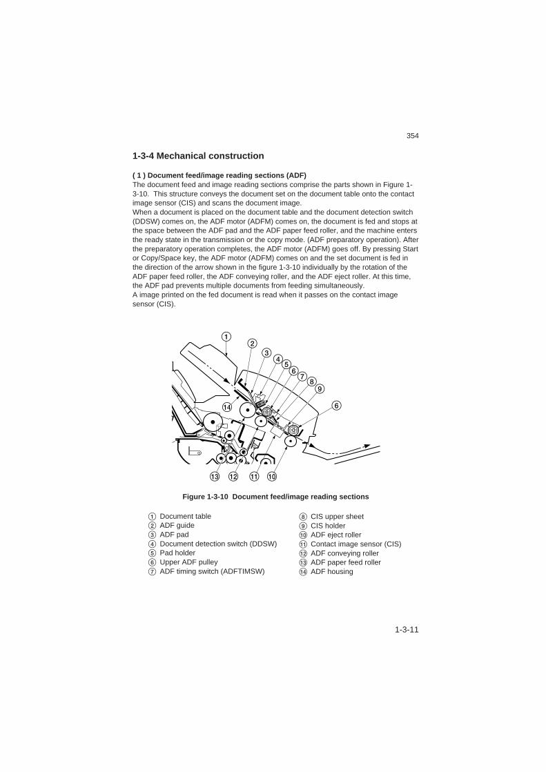
1-3-4 Mechanical construction
( 1 ) Document feed/image reading sections (ADF)The document feed and image reading sections comprise the parts shown in Figure 1-3-10. This structure conveys the document set on the document table onto the contactimage sensor (CIS) and scans the document image.When a document is placed on the document table and the document detection switch(DDSW) comes on, the ADF motor (ADFM) comes on, the document is fed and stops atthe space between the ADF pad and the ADF paper feed roller, and the machine entersthe ready state in the transmission or the copy mode. (ADF preparatory operation). Afterthe preparatory operation completes, the ADF motor (ADFM) goes off. By pressing Startor Copy/Space key, the ADF motor (ADFM) comes on and the set document is fed inthe direction of the arrow shown in the figure 1-3-10 individually by the rotation of theADF paper feed roller, the ADF conveying roller, and the ADF eject roller. At this time,the ADF pad prevents multiple documents from feeding simultaneously.A image printed on the fed document is read when it passes on the contact imagesensor (CIS).
1
! 0
$
23
45678
9
6
@#
Figure 1-3-10 Document feed/image reading sections
1 Document table2 ADF guide3 ADF pad4 Document detection switch (DDSW)5 Pad holder6 Upper ADF pulley7 ADF timing switch (ADFTIMSW)
8 CIS upper sheet9 CIS holder0 ADF eject roller! Contact image sensor (CIS)@ ADF conveying roller# ADF paper feed roller$ ADF housing
354
1-3-12
DDSW
ADFTIMSW
CIS
ADFM
CPCB
CN11-11
CN11-14
CN15-1~CN15-10
CN13-1 ~CN13-6
Figure 1-3-11 Document feed/image reading sections block diagram
354
1-3-13
( 2 ) Paper feed sectionThe paper feed section comprises the parts shown in Figure 1-3-12. This mechanismconveys the paper set on the paper feed tray to the imaging unit and transfer/chargeerasing sections synchronized with the image writing timing.
1
2 3
45
6
9 78
Figure 1-3-12 Paper feed section
1 Paper feed tray2 Paper size switch (PSSW)3 Paper feed pulley4 Paper feed switch (FSW)5 Upper feed roller
6 Transfer guide7 Lower feed roller8 Paper feed pad9 Pad holder
354
1-3-14
CN17-2
CN17-6
CN5-1
CN6-1 ~CN6-6
CPCB FSOL FSW
PSSW
MM
Figure 1-3-13 Paper feed section block diagram
MM
FSOL
OFF
Full speed
3 s
3 s
M. SYNC signal: ON
A
B
C0.6 s *1
Timing chart 1-3-1 Paper feed
• Paper feedA When the polygon motor (PM) reaches the specified rotation rate and the M.SYNC
signal comes on, the main motor (MM) comes on, the machine drive starts, and theupper and lower feed rollers start rotating.*1: In this time, the main motor (MM) starts rotating at minimum speed, its speed
increases in steps, and after about 0.6 s, it reaches full speed (the specifiedrotation rate).
B 3 s after M.SYNC signal comes on, the paper feed solenoid (FSOL) comes on, thepaper feed pulley rotates, and the paper feed starts.
C 3 s later, the paper feed solenoid (FSOL) goes off and the paper feed pulley rotationstops. Subsequently, the paper is conveyed to the imaging unit and the transfer/charge erasing sections by the upper and lower feed rollers.
354
1-3-15
( 3 ) Laser scanning unitThe laser scanning unit comprises the parts shown in Figure 1-3-14, 1-3-15.The laser scanning unit projects onto the drum surface the laser beam emitted from thelaser diode which is turned on or off according to a laser control signal (LD signal) fromthe control PCB (CPCB).This forms a static latent image on the drum surface exposed to the laser beam.
1
3
4
5
6
789
0
!
@
#
2
Figure 1-3-14 Laser scanning unit ( 1 )
1 Cover2 Polygon motor control board3 Mirror4 Polygon mirror5 Polygon motor (PM)6 Lens7 BD sensor
8 Correction cylinder lens9 Laser diode board (with BD sensor)0 Cylindrical lens! Lens@ Mirror# BD sensor mirror

354
1-3-16
12 3
9
0
4 68
5
6
7
to Drum
to Drum
Figure 1-3-15 Laser scanning unit ( 2 )
1 Laser diode............................... Emits a laser beam to form a latent electrostaticimage onto the drum surface.
2 Collimator lens.......................... Collimates the laser beam.3 Cylindrical lens ......................... Shapes the collimated laser beam to suit the
printing resolution.4 Mirror ........................................ Reflects the laser beam onto the polygon mirror.5 Polygon mirror .......................... Six-face mirror that revolves at approx.8504 rpm
with each face deflecting the laser beam for onehorizontal scan.
6 Lens.......................................... Corrects for the laser beam scanning speed whichbecomes greater closer to the drum edge (Keepingthe beam diameter constant), and corrects for thevertical inclination of the polygon mirror to ensurethat all the focal points of the laser beam are on thesame plane.
7 Mirror ........................................ Reflects the laser beam onto the drum surface.8 BD sensor mirror ...................... Reflects the laser beam to the BD sensor to the
horizontal synchronous signal.9 Correction cylinder lens ............ Corrects for the deviation of the laser beam
reflected onto the BD sensor.0 BD sensor................................. Detects the laser beam to output the beam detect
signal to the control PCB (C PCB) to provide timingfor the horizontal synchronous signal (HSYNC)inside the control PCB.
354
1-3-17
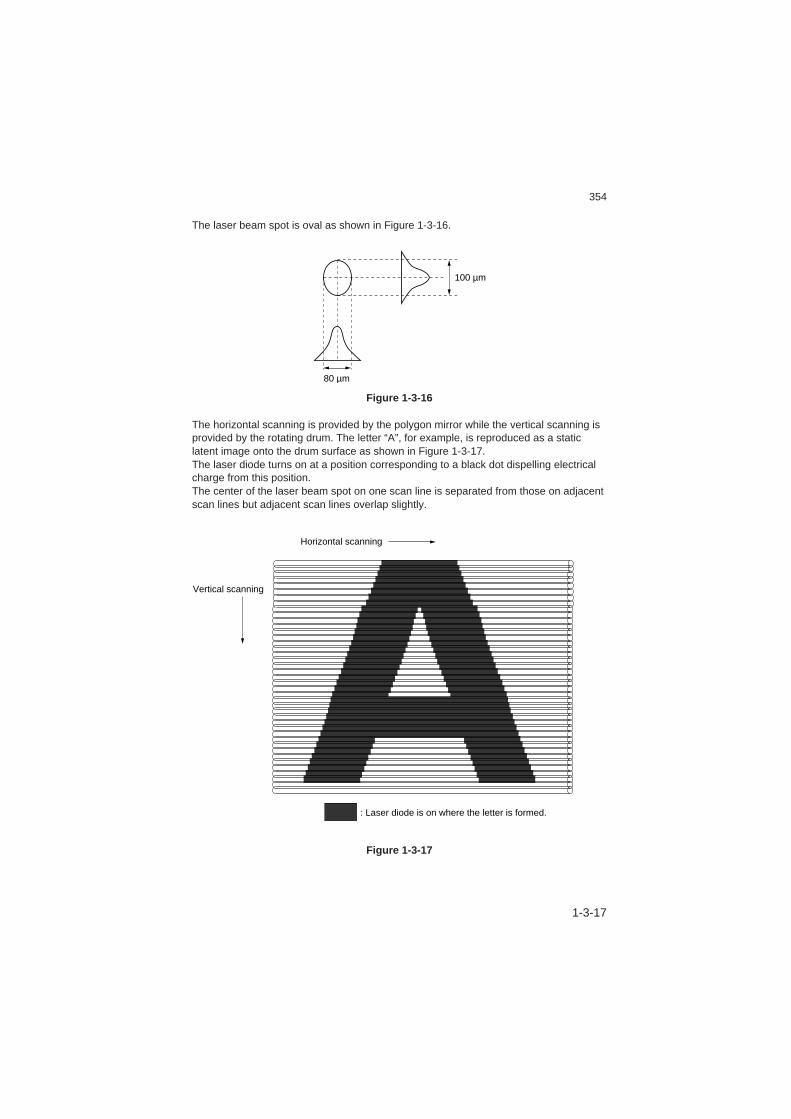
The laser beam spot is oval as shown in Figure 1-3-16.
100 µm
80 µm
Figure 1-3-16
The horizontal scanning is provided by the polygon mirror while the vertical scanning isprovided by the rotating drum. The letter “A”, for example, is reproduced as a staticlatent image onto the drum surface as shown in Figure 1-3-17.The laser diode turns on at a position corresponding to a black dot dispelling electricalcharge from this position.The center of the laser beam spot on one scan line is separated from those on adjacentscan lines but adjacent scan lines overlap slightly.
Horizontal scanning
Vertical scanning
: Laser diode is on where the letter is formed.
Figure 1-3-17
354
1-3-18
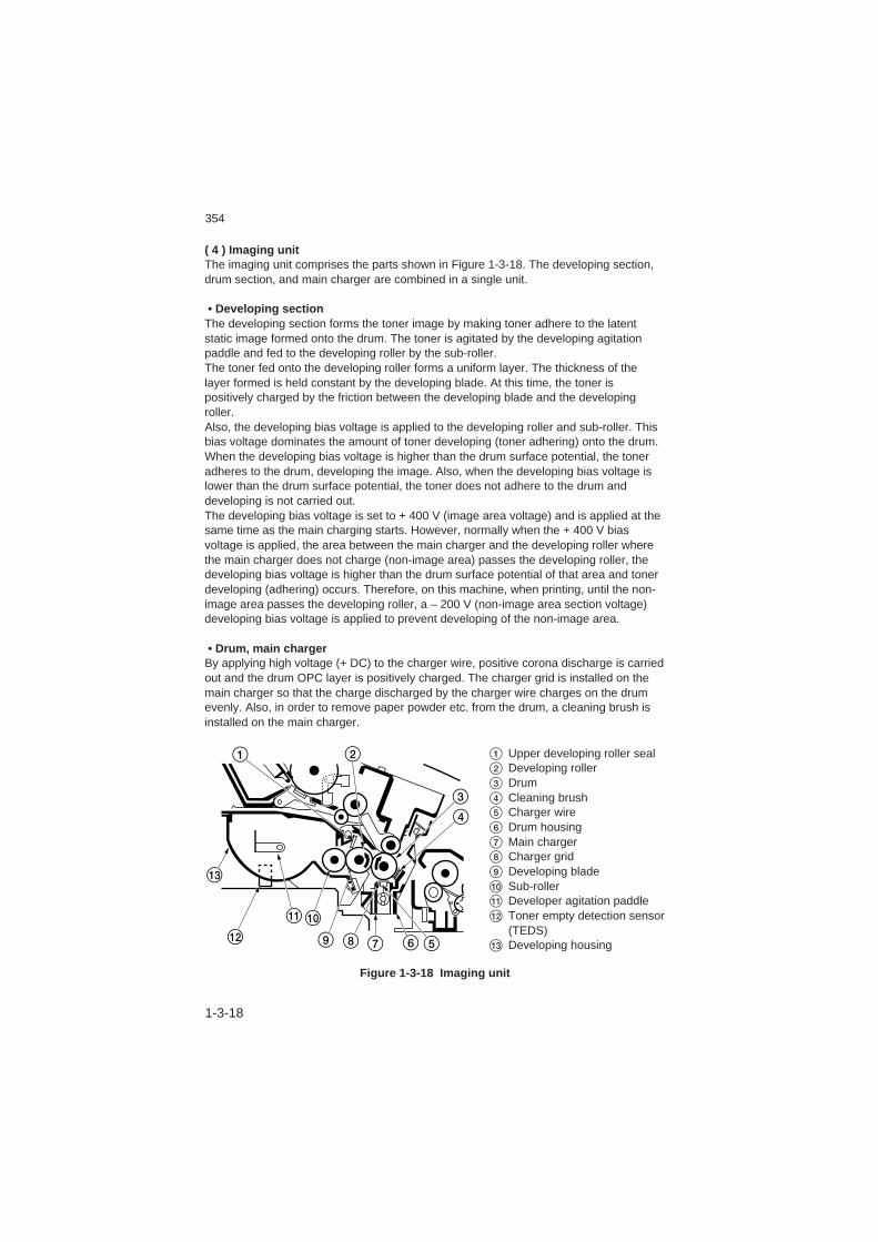
( 4 ) Imaging unitThe imaging unit comprises the parts shown in Figure 1-3-18. The developing section,drum section, and main charger are combined in a single unit.
• Developing sectionThe developing section forms the toner image by making toner adhere to the latentstatic image formed onto the drum. The toner is agitated by the developing agitationpaddle and fed to the developing roller by the sub-roller.The toner fed onto the developing roller forms a uniform layer. The thickness of thelayer formed is held constant by the developing blade. At this time, the toner ispositively charged by the friction between the developing blade and the developingroller.Also, the developing bias voltage is applied to the developing roller and sub-roller. Thisbias voltage dominates the amount of toner developing (toner adhering) onto the drum.When the developing bias voltage is higher than the drum surface potential, the toneradheres to the drum, developing the image. Also, when the developing bias voltage islower than the drum surface potential, the toner does not adhere to the drum anddeveloping is not carried out.The developing bias voltage is set to + 400 V (image area voltage) and is applied at thesame time as the main charging starts. However, normally when the + 400 V biasvoltage is applied, the area between the main charger and the developing roller wherethe main charger does not charge (non-image area) passes the developing roller, thedeveloping bias voltage is higher than the drum surface potential of that area and tonerdeveloping (adhering) occurs. Therefore, on this machine, when printing, until the non-image area passes the developing roller, a – 200 V (non-image area section voltage)developing bias voltage is applied to prevent developing of the non-image area.
• Drum, main chargerBy applying high voltage (+ DC) to the charger wire, positive corona discharge is carriedout and the drum OPC layer is positively charged. The charger grid is installed on themain charger so that the charge discharged by the charger wire charges on the drumevenly. Also, in order to remove paper powder etc. from the drum, a cleaning brush isinstalled on the main charger.
Figure 1-3-18 Imaging unit
1 Upper developing roller seal2 Developing roller3 Drum4 Cleaning brush5 Charger wire6 Drum housing7 Main charger8 Charger grid9 Developing blade0 Sub-roller! Developer agitation paddle@ Toner empty detection sensor
(TEDS)# Developing housing
1 2
34
56789
0!
#
@
354
1-3-19
Main charger
DrumDeveloping roller
Sub-roller
CPCB
CN4-2
CN4-4
CN3-2
CN1-2
CN1-4
MC/DB1 REM
DB CHG1
CN4-5CN1-5 DB CHG2
CN4-6CN1-6 ALARM
HVTPCB
TEDS
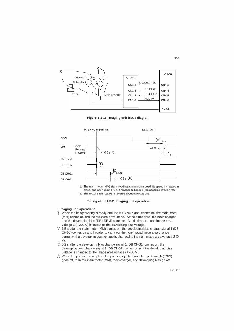
Figure 1-3-19 Imaging unit block diagram
MM
ESW
0.6 s *1*2
4 s
A
D
0.5 s
DB CHG1
DB CHG2
DB1 REM
MC REM
1.5 s
0.2 s
B
C
OFFForwardReverse
M. SYNC signal: ON ESW: OFF
*1: The main motor (MM) starts rotating at minimum speed, its speed increases insteps, and after about 0.6 s, it reaches full speed (the specified rotation rate).
*2: The motor shaft rotates in reverse about two rotations.
Timing chart 1-3-2 Imaging unit operation
• Imaging unit operationsA When the image writing is ready and the M.SYNC signal comes on, the main motor
(MM) comes on and the machine drive starts. At the same time, the main chargerand the developing bias (DB1 REM) come on. At this time, the non-image areavoltage 1 (– 200 V) is output as the developing bias voltage.
B 1.5 s after the main motor (MM) comes on, the developing bias change signal 1 (DBCHG1) comes on and in order to carry out the non-image/image area changecorrectly, the developing bias voltage is changed to the non-image area voltage 2 (0V).
C 0.2 s after the developing bias change signal 1 (DB CHG1) comes on, thedeveloping bias change signal 2 (DB CHG2) comes on and the developing biasvoltage is changed to the image area voltage (+ 400 V).
D When the printing is complete, the paper is ejected, and the eject switch (ESW)goes off, then the main motor (MM), main charger, and developing bias go off.
354
1-3-20
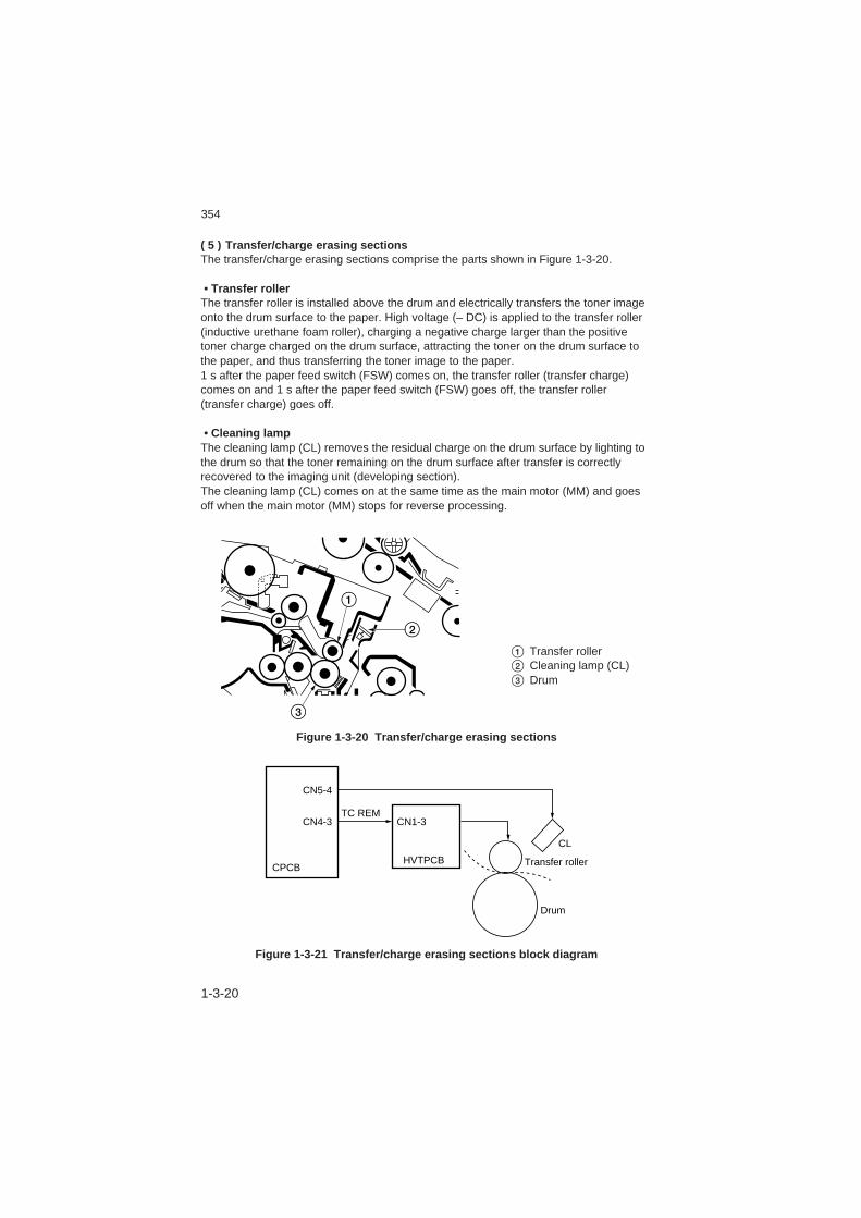
( 5 ) Transfer/charge erasing sectionsThe transfer/charge erasing sections comprise the parts shown in Figure 1-3-20.
• Transfer rollerThe transfer roller is installed above the drum and electrically transfers the toner imageonto the drum surface to the paper. High voltage (– DC) is applied to the transfer roller(inductive urethane foam roller), charging a negative charge larger than the positivetoner charge charged on the drum surface, attracting the toner on the drum surface tothe paper, and thus transferring the toner image to the paper.1 s after the paper feed switch (FSW) comes on, the transfer roller (transfer charge)comes on and 1 s after the paper feed switch (FSW) goes off, the transfer roller(transfer charge) goes off.
• Cleaning lampThe cleaning lamp (CL) removes the residual charge on the drum surface by lighting tothe drum so that the toner remaining on the drum surface after transfer is correctlyrecovered to the imaging unit (developing section).The cleaning lamp (CL) comes on at the same time as the main motor (MM) and goesoff when the main motor (MM) stops for reverse processing.
1
3
2
Figure 1-3-20 Transfer/charge erasing sections
Drum
Transfer rollerCPCB
TC REM
HVTPCB
CN1-3CN4-3
CN5-4
CL
Figure 1-3-21 Transfer/charge erasing sections block diagram
1 Transfer roller2 Cleaning lamp (CL)3 Drum

354
1-3-21
( 6 ) Fixing sectionThe fixing section comprises the parts shown in Figure 1-3-22. The fixing section usesheat and pressure to fuse the toner image transferred to the paper. The heat roller isheated by the fixing heater (H). During printing, the heat roller temperature is controlledto be a constant 160°C/320°F by switching the fixing heater on/off according to the heatroller surface temperature detected by the fixing thermistor (TH). When printing ends,the fixing heater (H) goes off.If the temperature becomes abnormally high, the fixing thermistor (TH) detects the hightemperature abnormality, fixing thermostats 1 and 2 (FTH1, 2) go off, and the powersupply to the fixing heater (H) is cut off.The press roller is pressed against the heat roller by the press springs at both ends. Thepressure between the press roller and heat roller is approx. 39.2 N (19.6 N one side).
• Separating the paper from the heat rollerThere are two separation claws on the fixing unit lower housing. When the paperpasses the fixing section, they prevent the paper from sticking to the heat roller andwrapping around it. The separation claws are constantly pressed in the direction ofcontact with the heat roller by the separation claw spring.
1
3
4
5678
2
9
0
Figure 1-3-22 Fixing section
1 Fixing unit upper housing2 Press roller3 Eject pulley4 Eject roller5 Separation claw
6 Eject switch (ESW)7 Heat roller8 Fixing thermistor (TH)9 Fixing unit lower housing0 Fixing heater (H)

354
1-3-22
NoiseFilter
Heatercontrol circuit
PSPCBCN6-1CN5-1
CN1-10
CN3-1
CN2-1AC input
FTH2 FTH1 H
TH
CPCB
CN18-1
CN1-7H REMNEUTRAL
LIVEFuse
Fuse
Figure 1-3-23 Fixing section block diagram
R
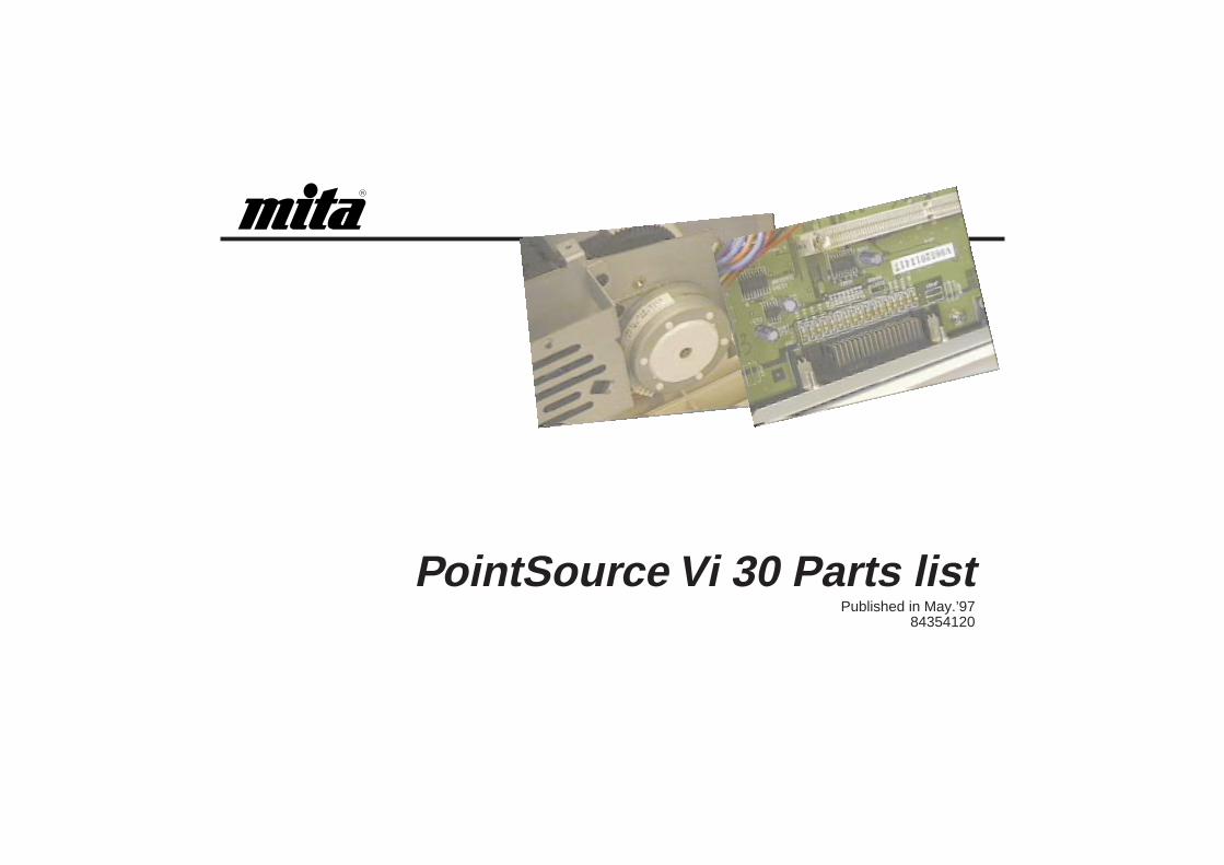
PointSource Vi 30 Parts listPublished in May.’97
84354120
FIG.1 EXTERIOR COVERS 4
FIG.2 FRAMES 6
FIG.3 PAPER FEED TRAY SECTION 8
FIG.4 DRIVING SECTION 10
FIG.5 CHARGING SECTION 12
FIG.6 FIXING SECTION 14
FIG.7 ELECTRICAL COMPONENTS 16
FIG.8 PAPER FEED SECTION 18
FIG.9 IMAGING UNIT 20
FIG.10 ACCESSORIES AND OPTION 22
FIG.11 SPECIFIED PARTS FOR EACH COUNTRY 24
• INDEX 26
Contents

1
2
3
4
5
6
7
1
2
3
4
5
6
7
A B C D E F G H I J
A B C D E F G H I J
354
– 4 –
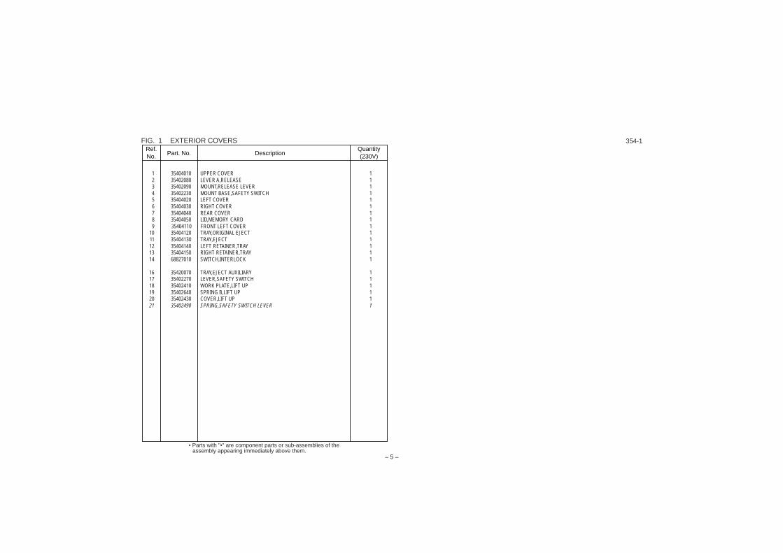
FIG. 1 EXTERIOR COVERS
7
5
9
12
11
10
13
4 1714
18
19
20
6
8
1
3
2
16
HCD
HCD
HCD
HCD
HCD
HCD
BBB
HCD
HCD
21
354-1
Part. No. DescriptionQuantity(230V)
Ref.No. Part. No. Description
Quantity(230V)
Ref.No.
354
– 5 –
• Parts with "•" are component parts or sub-assemblies of theassembly appearing immediately above them.
1 35404010 UPPER COVER 12 35402080 LEVER A,RELEASE 13 35402090 MOUNT,RELEASE LEVER 14 35402230 MOUNT BASE,SAFETY SWITCH 15 35404020 LEFT COVER 16 35404030 RIGHT COVER 17 35404040 REAR COVER 18 35404050 LID,MEMORY CARD 19 35404110 FRONT LEFT COVER 1
10 35404120 TRAY,ORIGINAL EJECT 111 35404130 TRAY,EJECT 112 35404140 LEFT RETAINER,TRAY 113 35404150 RIGHT RETAINER,TRAY 114 68827010 SWITCH,INTERLOCK 1
16 35420070 TRAY,EJECT AUXILIARY 117 35402270 LEVER,SAFETY SWITCH 118 35402410 WORK PLATE,LIFT UP 119 35402640 SPRING B,LIFT UP 120 35402430 COVER,LIFT UP 121 35402490 SPRING,SAFETY SWITCH LEVER 1
FIG. 1 EXTERIOR COVERS 354-1
1
2
3
4
5
6
7
1
2
3
4
5
6
7
A B C D E F G H I J
A B C D E F G H I J
354
– 6 –
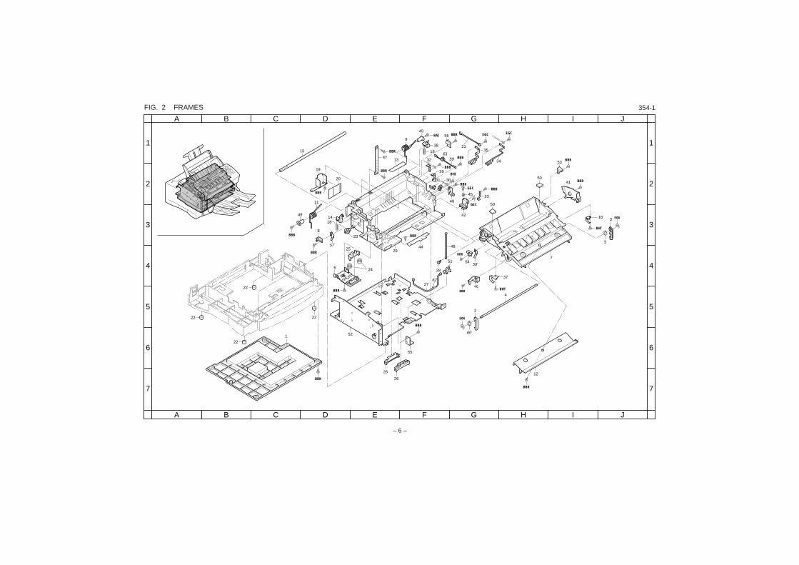
FIG. 2 FRAMES
7
60
E04
2762
38
1347
18
49
9
BBR
BAI
20
19
15
BBR
49
11
1418
BBR
BBB
122
22
22
22
BBK
26
26
55
4429
6 24
BBR
2
4
28
BBB
46BBR
BBR
12
37
51 54
48
BHT
BBR
16
5
3
41
53
50
50
BBR
BBR
BHT
E04
59
39
45 33
32
56
BBB
BBB
BBR EGC EGC
GEC
BHI
21
3031BBK
BBR
8
25
23 BBR
40
42
GEC
52
35
34
57
58
61BBB
354-1
Part. No. DescriptionQuantity(230V)
Ref.No. Part. No. Description
Quantity(230V)
Ref.No.
354
– 7 –
• Parts with "•" are component parts or sub-assemblies of theassembly appearing immediately above them.
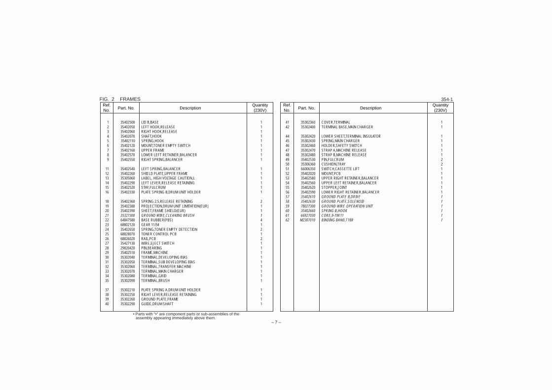
FIG. 2 FRAMES
1 35402500 LID B,BASE 12 35402050 LEFT HOOK,RELEASE 13 35402060 RIGHT HOOK,RELEASE 14 35402070 SHAFT,HOOK 15 35402110 SPRING,HOOK 16 35402120 MOUNT,TONER EMPTY SWITCH 17 35402160 UPPER FRAME 18 35402570 LOWER LEFT RETAINER,BALANCER 19 35402550 RIGHT SPRING,BALANCER 1
11 35402540 LEFT SPRING,BALANCER 112 35402260 SHIELD PLATE,UPPER FRAME 113 35305060 LABEL, HIGH VOLTAGE CAUTION,L 114 35402290 LEFT LEVER,RELEASE RETAINING 115 35402520 STAY,FULCRUM 116 35402330 PLATE SPRING B,DRUM UNIT HOLDER 1
18 35402360 SPRING 2.5,RELEASE RETAINING 219 35402380 PROJECTION,DRUM UNIT LIMITATION(EUR) 120 35402390 SHEET,FRAME SHIELD(EUR) 121 35327300 GROUND WIRE,CLEANING BRUSH 122 64847580 BASE RUBBER(PBS) 423 68802120 GEAR 11/34 124 35402650 SPRING,TONER EMPTY DETECTION 225 68828070 TONER CONTROL PCB 126 68826020 RAIL,PCB 227 35427130 WIRE,EJECT SWITCH 128 29820420 PIN,BEARING 129 35402510 FRAME,MACHINE 130 35302040 TERMINAL,DEVELOPING BIAS 131 35302050 TERMINAL,SUB DEVELOPING BIAS 132 35302060 TERMINAL,TRANSFER MACHINE 133 35302070 TERMINAL,MAIN CHARGER 134 35302080 TERMINAL,GRID 135 35302090 TERMINAL,BRUSH 1
37 35302210 PLATE SPRING A,DRUM UNIT HOLDER 138 35302250 RIGHT LEVER,RELEASE RETAINING 139 35302260 GROUND PLATE,FRAME 140 35302290 GUIDE,DRUM SHAFT 1
41 35302360 COVER,TERMINAL 142 35302400 TERMINAL BASE,MAIN CHARGER 1
44 35302420 LOWER SHEET,TERMINAL INSULATOR 145 35302430 SPRING,MAIN CHARGER 146 35302460 HOLDER,SAFETY SWITCH 147 35302470 STRAP A,MACHINE RELEASE 148 35302480 STRAP B,MACHINE RELEASE 149 35402530 PIN,FULCRUM 250 35306360 CUSHION,TRAY 251 66006350 SWITCH,CASSETTE LIFT 152 35402020 MOUNT,PCB 153 35402580 UPPER RIGHT RETAINER,BALANCER 154 35402560 UPPER LEFT RETAINER,BALANCER 155 35402620 STOPPER,JOINT 156 35402590 LOWER RIGHT RETAINER,BALANCER 157 35402610 GROUND PLATE B,DRIVE 158 35402630 GROUND PLATE,SOLENOID 159 78027300 GROUND WIRE OPERATION UNIT 160 35402660 SPRING B,HOOK 161 66927030 CORE,9-19X11 162 M2307010 BINDING BAND,T18R 1
354-1
1
2
3
4
5
6
7
1
2
3
4
5
6
7
A B C D E F G H I J
A B C D E F G H I J
354
– 8 –
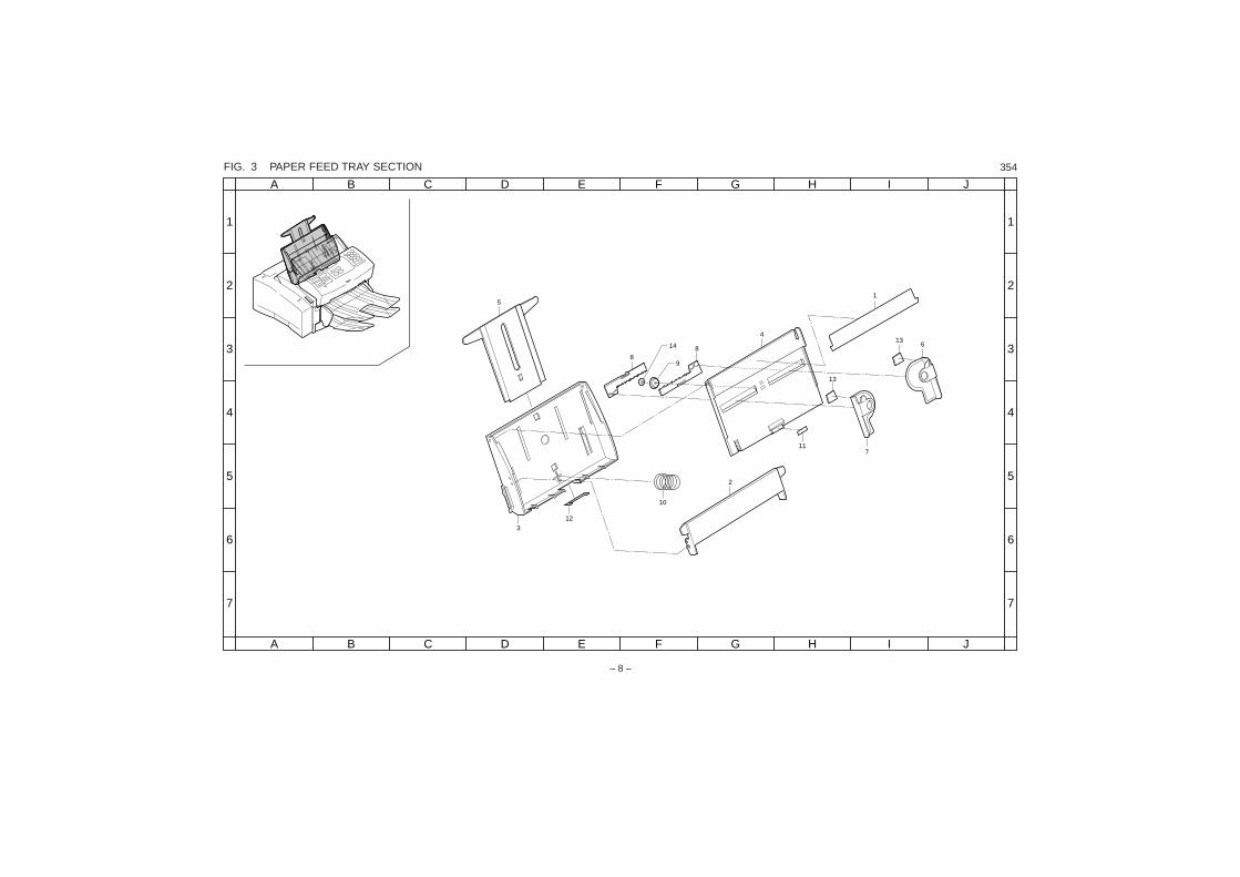
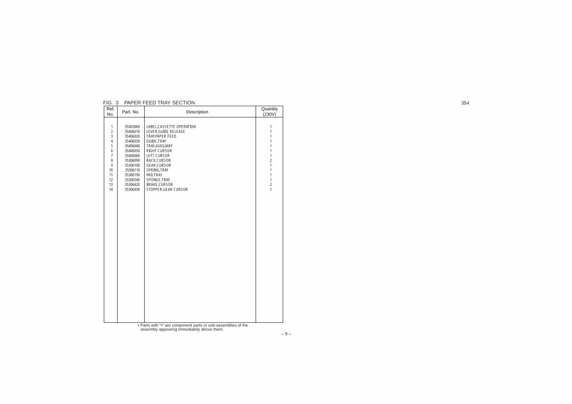
FIG. 3 PAPER FEED TRAY SECTION
5
88
9
14
312
10
2
11
4
1
13
13
6
7
Part. No. DescriptionQuantity(230V)
Ref.No. Part. No. Description
Quantity(230V)
Ref.No.
354
– 9 –
• Parts with "•" are component parts or sub-assemblies of theassembly appearing immediately above them.
FIG. 3 PAPER FEED TRAY SECTION
1 35405060 LABEL,CASSETTE OPERATION 12 35406010 LEVER,GUIDE RELEASE 13 35406020 TRAY,PAPER FEED 14 35406030 GUIDE,TRAY 15 35406040 TRAY,AUXILIARY 16 35406050 RIGHT CURSOR 17 35406060 LEFT CURSOR 18 35306090 RACK,CURSOR 29 35306100 GEAR,CURSOR 1
10 35306110 SPRING,TRAY 111 35306190 PAD,TRAY 112 35306340 SPONGE,TRAY 113 35306420 BRAKE,CURSOR 214 35306430 STOPPER,GEAR CURSOR 1

1
2
3
4
5
6
7
1
2
3
4
5
6
7
A B C D E F G H I J
A B C D E F G H I J
354
– 10 –
FIG. 4 DRIVING SECTION
49
24
50 11 10
1312 5
20
19
34 35
33
3236
6
39
37
38
42
41
4346
4544
48
47
40
9
8
7
9
15
1454
16
28
26
25
5130
23
21
21
23
1718
1
25
2
22
3
29
4
50
BBB
BHT
BHI
E05
E05
E05
E05
E05
E05
BBABBB
BBB
KAM
KAM
55
56
57
58
59
59
60
BBB
53
61 61
354-1
Part. No. DescriptionQuantity(230V)
Ref.No. Part. No. Description
Quantity(230V)
Ref.No.
354
– 11 –
• Parts with "•" are component parts or sub-assemblies of theassembly appearing immediately above them.
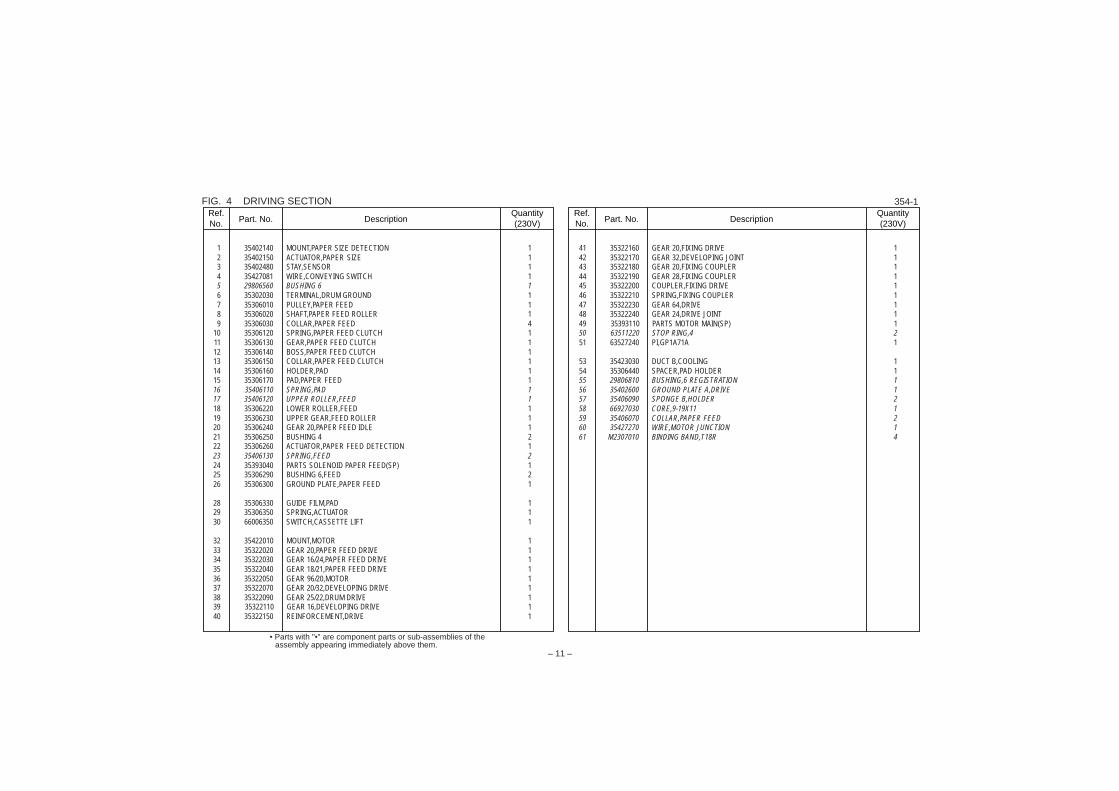
FIG. 4 DRIVING SECTION
1 35402140 MOUNT,PAPER SIZE DETECTION 12 35402150 ACTUATOR,PAPER SIZE 13 35402480 STAY,SENSOR 14 35427081 WIRE,CONVEYING SWITCH 15 29806560 BUSHING 6 16 35302030 TERMINAL,DRUM GROUND 17 35306010 PULLEY,PAPER FEED 18 35306020 SHAFT,PAPER FEED ROLLER 19 35306030 COLLAR,PAPER FEED 4
10 35306120 SPRING,PAPER FEED CLUTCH 111 35306130 GEAR,PAPER FEED CLUTCH 112 35306140 BOSS,PAPER FEED CLUTCH 113 35306150 COLLAR,PAPER FEED CLUTCH 114 35306160 HOLDER,PAD 115 35306170 PAD,PAPER FEED 116 35406110 SPRING,PAD 117 35406120 UPPER ROLLER,FEED 118 35306220 LOWER ROLLER,FEED 119 35306230 UPPER GEAR,FEED ROLLER 120 35306240 GEAR 20,PAPER FEED IDLE 121 35306250 BUSHING 4 222 35306260 ACTUATOR,PAPER FEED DETECTION 123 35406130 SPRING,FEED 224 35393040 PARTS SOLENOID PAPER FEED(SP) 125 35306290 BUSHING 6,FEED 226 35306300 GROUND PLATE,PAPER FEED 1
28 35306330 GUIDE FILM,PAD 129 35306350 SPRING,ACTUATOR 130 66006350 SWITCH,CASSETTE LIFT 1
32 35422010 MOUNT,MOTOR 133 35322020 GEAR 20,PAPER FEED DRIVE 134 35322030 GEAR 16/24,PAPER FEED DRIVE 135 35322040 GEAR 18/21,PAPER FEED DRIVE 136 35322050 GEAR 96/20,MOTOR 137 35322070 GEAR 20/32,DEVELOPING DRIVE 138 35322090 GEAR 25/22,DRUM DRIVE 139 35322110 GEAR 16,DEVELOPING DRIVE 140 35322150 REINFORCEMENT,DRIVE 1
41 35322160 GEAR 20,FIXING DRIVE 142 35322170 GEAR 32,DEVELOPING JOINT 143 35322180 GEAR 20,FIXING COUPLER 144 35322190 GEAR 28,FIXING COUPLER 145 35322200 COUPLER,FIXING DRIVE 146 35322210 SPRING,FIXING COUPLER 147 35322230 GEAR 64,DRIVE 148 35322240 GEAR 24,DRIVE JOINT 149 35393110 PARTS MOTOR MAIN(SP) 150 63511220 STOP RING,4 251 63527240 PI,GP1A71A 1
53 35423030 DUCT B,COOLING 154 35306440 SPACER,PAD HOLDER 155 29806810 BUSHING,6 REGISTRATION 156 35402600 GROUND PLATE A,DRIVE 157 35406090 SPONGE B,HOLDER 258 66927030 CORE,9-19X11 159 35406070 COLLAR,PAPER FEED 260 35427270 WIRE,MOTOR JUNCTION 161 M2307010 BINDING BAND,T18R 4
354-1
1
2
3
4
5
6
7
1
2
3
4
5
6
7
A B C D E F G H I J
A B C D E F G H I J
354
– 12 –
FIG. 5 CHARGING SECTION
3
8
7
4
6
5
9 11
86
5
1
9
10
2
BHT
11
354-1
Part. No. DescriptionQuantity(230V)
Ref.No. Part. No. Description
Quantity(230V)
Ref.No.
354
– 13 –
• Parts with "•" are component parts or sub-assemblies of theassembly appearing immediately above them.
FIG. 5 CHARGING SECTION
1 35402340 MOUNT,CLEANING LAMP 12 35416010 UPPER TERMINAL,TRANSFER 13 35306380 SEAL,PAPER DUST DISPOSAL 14 35316120 ROLLER,TRANSFER (METRIC) 15 35316020 BUSHING,TRANSFER 26 35316030 SPRING,TRANSFER 27 35316050 GUIDE,TRANSFER 18 35416020 SPRING,TRANSFER GUIDE 29 35316110 PULLEY C,TRANSFER ROLLER 2
10 35393132 PARTS LAMP CLEANING(SP) 111 35416030 SHEET,TRANSFER GUIDE FILM 2
354-1
1
2
3
4
5
6
7
1
2
3
4
5
6
7
A B C D E F G H I J
A B C D E F G H I J
354
– 14 –
FIG. 6 FIXING SECTION
17
29
30
11
1
17
2919
19
8
8
62
30
9
5
4
23
24
21
28 13
16
14
12
18
18
20
2225
7
7
10
1526
27
31
BBR
BBR
BBR
BBB
BBB
BBB
BBB
RDC
3
354-1
Part. No. DescriptionQuantity(230V)
Ref.No. Part. No. Description
Quantity(230V)
Ref.No.
354
– 15 –
• Parts with "•" are component parts or sub-assemblies of theassembly appearing immediately above them.
FIG. 6 FIXING SECTION
1 35405080 CAUTION LABEL,HIGH TEMPERATURE (EXP) 12 35493100 PARTS HEATER 230 FIXING(SP) 13 35400020 EJECT ROLLER ASS’Y 14 35393070 PARTS ROLLER HEAT(SP) 15 35320030 BUSHING,HEAT ROLLER 16 35393080 PARTS ROLLER PRESSURE(SP) 17 35320071 SEPARATION CLAW,HEAT ROLLER 28 35320081 PULLEY,EJECT 29 35320090 GEAR,HEAT ROLLER 1
10 35320100 GEAR,FIXING IDLE 111 35420040 UPPER HOUSING,FIXING 112 35420050 LOWER HOUSING,FIXING 113 35320130 TERMINAL,THERMOSTAT 114 35320140 FRONT TERMINAL,FIXING 115 35320150 REAR TERMINAL A,FIXING 116 35320160 REAR TERMINAL B,HEATER 117 35320170 SPRING,FIXING PRESSURE 218 35320180 SPRING,SEPARATION CLAW 219 35320190 SPRING,EJECT PULLEY 220 35320220 GROUND PLATE,HEAT ROLLER 121 35320250 THERMISTOR,FIXING 122 35420060 ACTUATOR,EJECT SWITCH 123 35320280 THERMAL PROTECTOR A 124 35320290 THERMAL PROTECTOR B 125 35320300 SPRING,EJECT ACTUATOR 126 35320310 GEAR,EJECT ROLLER 127 35320320 BUSHING B,HEAT ROLLER 128 35320360 FILM,FIXING THERMISTOR 129 35320370 HOLDER,PRESS ROLLER BEARING 230 35320380 BEARING,PRESS ROLLER 231 29820420 PIN,BEARING 1
354-1
1
2
3
4
5
6
7
1
2
3
4
5
6
7
A B C D E F G H I J
A B C D E F G H I J
354
– 16 –
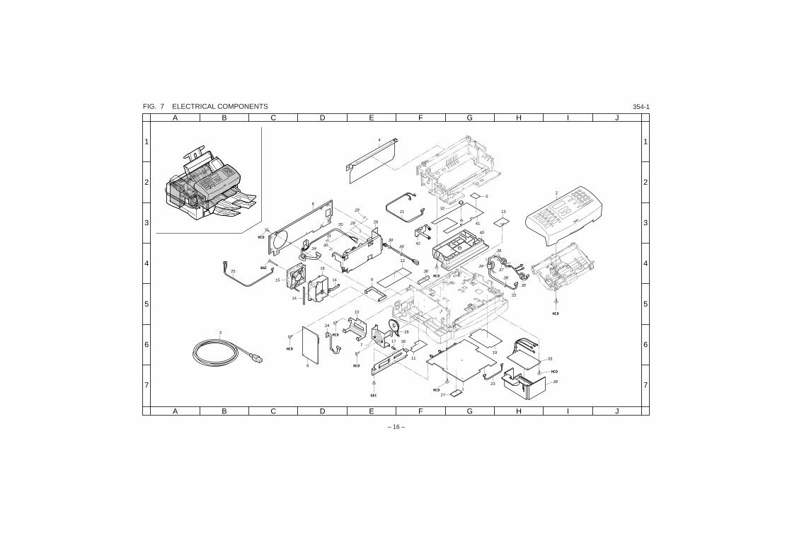
FIG. 7 ELECTRICAL COMPONENTS
8
25
3
16
9
10
7
24
26
18
11
15
2829
29
31
30
14
14
17
127
23
19
33
38
42
21
41
1332
52
6
12
40
4
HCD
HCD
HCD
HCD
HCD
HCD
GEC
HCD
HCD
BAZ
20
34
36
39
39
22
35
3734
39
39
354-1

Part. No. DescriptionQuantity(230V)
Ref.No. Part. No. Description
Quantity(230V)
Ref.No.
354
– 17 –
• Parts with "•" are component parts or sub-assemblies of theassembly appearing immediately above them.
FIG. 7 ELECTRICAL COMPONENTS
1 35401011 CONTROLLER ASS’Y 12 35493030 PARTS OPERATION UNIT (EUR)SP 13 76227030 POWER CORD(220) 14 35402350 SHIELD PLATE,MACHINE BASE 15 67305310 CAUTION LABEL,HV 16 35401050 NCU ASS’Y (EUR) 17 35402190 MOUNT,SPEAKER 18 35402220 REAR MOUNT,COVER 19 35402310 MOUNT A,NCU PCB 1
10 35402320 MOUNT B,NCU PCB 111 35402440 WIND SHIELD PLATE A,MOUNT PCB 112 35402450 WIND SHIELD PLATE B,MOUNT PCB 113 35402460 WIND SHIELD PLATE C,MOUNT PCB 114 35402470 SPONGE,DUCT 215 35493040 PARTS FAN COOLING (SP) 116 35423020 DUCT,COOLING 117 M0008000 SPACER,178877-2(AMP) 218 35426020 MOUNT,CONNECTOR 119 35426030 INSULATING PLATE,HIGH VOLTAGE PCB 120 35427021 WIRE,POWER SOURCE 121 35427031 WIRE,LSU 122 35427051 WIRE,OPERATION UNIT 123 35427071 WIRE,HIGH VOLTAGE 124 35427091 WIRE,NCU 125 35427111 WIRE,SOLENOID 126 35493060 PARTS SPEAKER (SP) 127 35493070 PARTS IC ROM (SP) 128 35428041 POWER SOURCE PCB (230) 129 •M1753010 FUSE,S506-3.15A(BUSSMANN) 230 •M1752000 FUSE,S506-2.5A(BUSSMANN) 131 •M1752010 FUSE,GDB-2A(BUSSMANN) 132 35312040 CAP,LSU 133 35328033 HIGH VOLTAGE UNIT PCB 134 61527170 FERRITE CORE TR 235 66927030 CORE,9-19X11 136 35427280 SHIELD,GASKET 237 73827030 LINE FILTER ESDR-25 138 35404160 COVER,HIGH VOLTAGE PCB 139 M2307010 BINDING BAND,T18R 440 35393050 PARTS UNIT SCANNER(SP) 1
354-1
41 35312020 COVER,LSU 142 35312030 GROUND PLATE,LSU 1
1
2
3
4
5
6
7
1
2
3
4
5
6
7
A B C D E F G H I J
A B C D E F G H I J
354
– 18 –
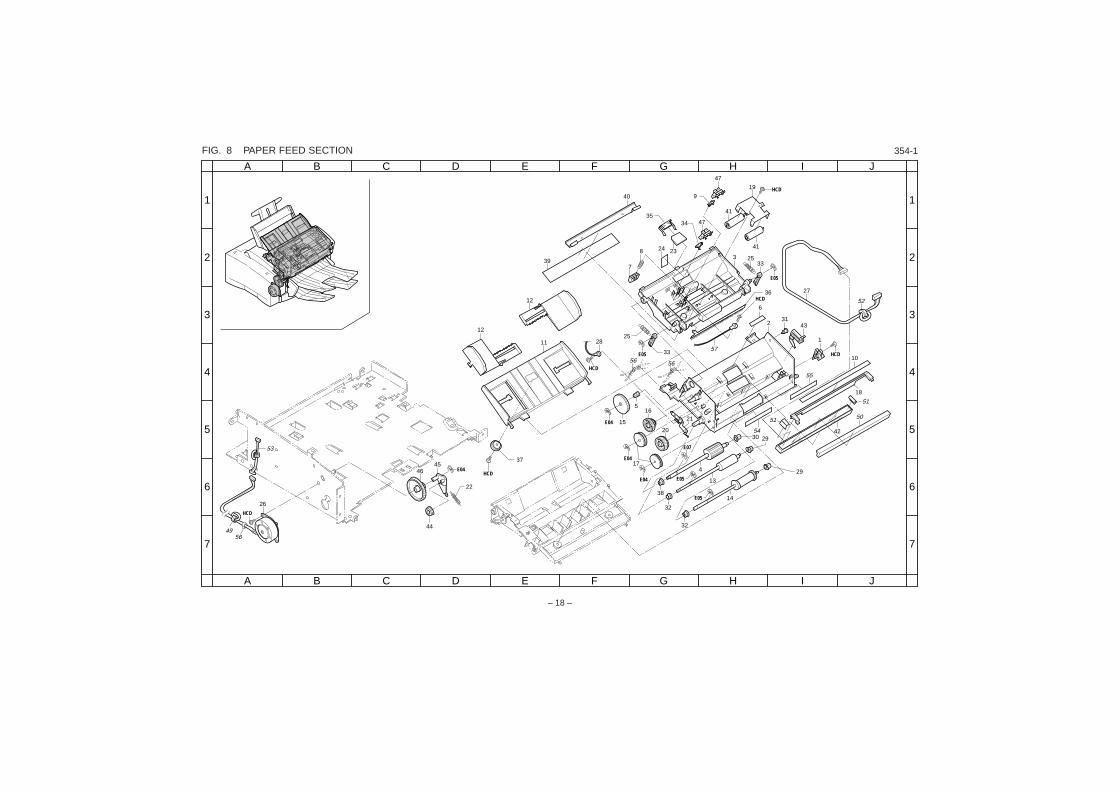
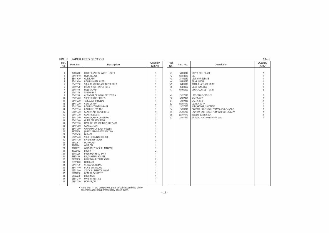
FIG. 8 PAPER FEED SECTION
4645
44
22
37
40
39
248
7
35
9
47
4734
23
19
41
41
25
25
33
6
3
231
43
36
285733
10
1
18
42
14
17
13
38
32
32
16
15
5
20
21
4
30 29
29
11
12
12
E04
E04
E05
E04
E04
E07
E05
E05
E05
HCD
HCD
HCD
HCD
HCD
26
49
HCD
51
51
50
54
55
27
52
53
56
5656
354-1
Part. No. DescriptionQuantity(230V)
Ref.No. Part. No. Description
Quantity(230V)
Ref.No.
354
– 19 –
• Parts with "•" are component parts or sub-assemblies of theassembly appearing immediately above them.
FIG. 8 PAPER FEED SECTION
1 35402280 HOLDER,SAFETY SWITCH LEVER 12 35411010 HOUSING,ADF 13 35411020 GUIDE,ADF 14 35411030 ROLLER,PAPER FEED 15 35411110 SQUARE SPRING,ADF PAPER FEED 16 35411120 FRONT SHEET,PAPER FEED 17 35411140 HOLDER,PAD 18 35411150 SPRING,PAD 19 35411160 ACTUATOR,ORIGINAL DETECTION 1
10 35411460 SHEET,GUIDE FILM CIS 111 35411220 TABLE,ADF ORIGINAL 112 35411230 CURSOR,ADF 213 35411300 ROLLER,CONVEYING ADF 114 35411310 ROLLER,EJECT ADF 115 35411320 GEAR 51,ADF PAPER FEED 116 35411330 GEAR 16/37,IDLE 117 35411340 GEAR 36,ADF CONVEYING 218 35411360 GUIDE,CIS RETAINING 119 35411370 UPPER PLATE SPRING,PULLEY ADF 120 35411380 GEAR 37,JOINT 121 35411390 GROUND PLATE,ADF ROLLER 122 78022030 JOINT SPRING DRIVE SECTION 123 35411410 PAD,ADF 124 35411420 SHEET,ORIGINAL HOLDER 125 35411430 SPRING,ADF HOOK 226 35427011 MOTOR,ADF 127 35427041 WIRE,CIS 128 35427151 WIRE,ADF STATIC ELIMINATOR 129 49028102 BUSH 4 230 29717230 BUSHING 6,FEED BACK 131 29804160 PIN,ORIGINAL HOLDER 132 29806810 BUSHING,6 REGISTRATION 233 63511080 HOOK,ADF 234 35411470 ACTUATOR,TIMING 135 35411440 PLATE SPRING,PAD 136 63511590 STATIC ELIMINATOR B,ADF 137 65907210 GEAR 20,CASSETTE 138 67322230 BUSHING 8 139 68811310 UPPER SHEET,CIS 140 68811330 HOLDER,CIS 1
41 68811342 UPPER PULLEY,ADF 242 68813010 CIS 143 35402250 LEVER B,RELEASE 144 35411070 GEAR 21,IDLE 145 35411100 WORK PLATE,ADF JOINT 146 35411350 GEAR 16/65,IDLE 147 66006350 SWITCH,CASSETTE LIFT 2
49 73827030 LINE FILTER ESDR-25 150 68811430 SHEET A,CIS 151 68811440 SHEET B,CIS 252 66927030 CORE,9-19X11 153 35427270 WIRE,MOTOR JUNCTION 154 35405140 CAUTION LABEL,HIGH TEMPERATURE A (EXP) 155 35405130 CAUTION LABEL,HIGH TEMPERATURE B (EXP) 156 M2307010 BINDING BAND,T18R 357 78027300 GROUND WIRE OPERATION UNIT 1
354-1
1
2
3
4
5
6
7
1
2
3
4
5
6
7
A B C D E F G H I J
A B C D E F G H I J
354
– 20 –
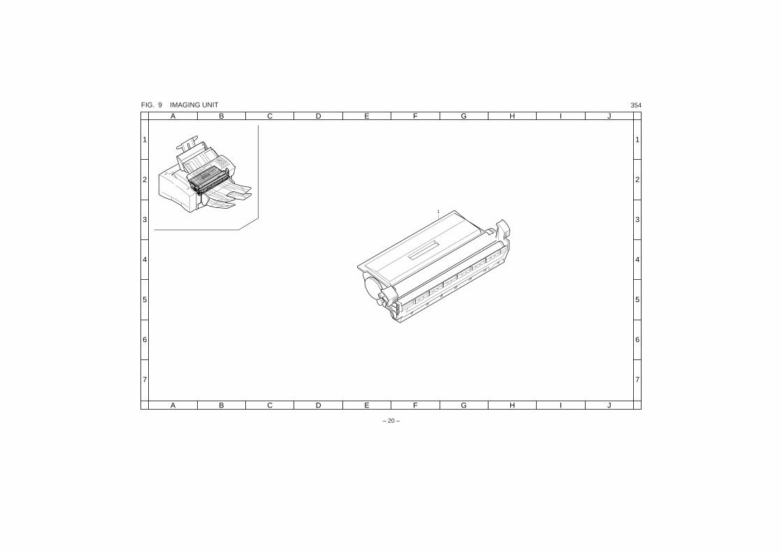
FIG. 9 IMAGING UNIT
1
Part. No. DescriptionQuantity(230V)
Ref.No. Part. No. Description
Quantity(230V)
Ref.No.
354
– 21 –
• Parts with "•" are component parts or sub-assemblies of theassembly appearing immediately above them.
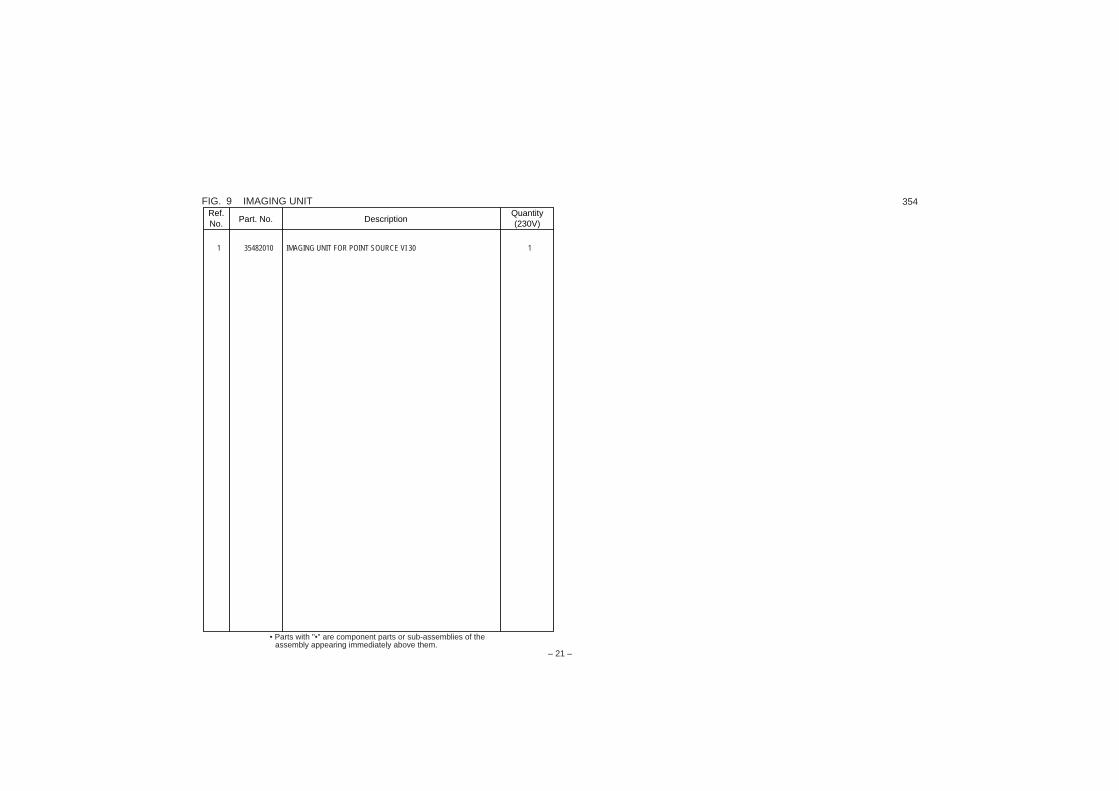
FIG. 9 IMAGING UNIT
1 35482010 IMAGING UNIT FOR POINT SOURCE VI 30 1
1
2
3
4
5
6
7
1
2
3
4
5
6
7
A B C D E F G H I J
A B C D E F G H I J
354
– 22 –
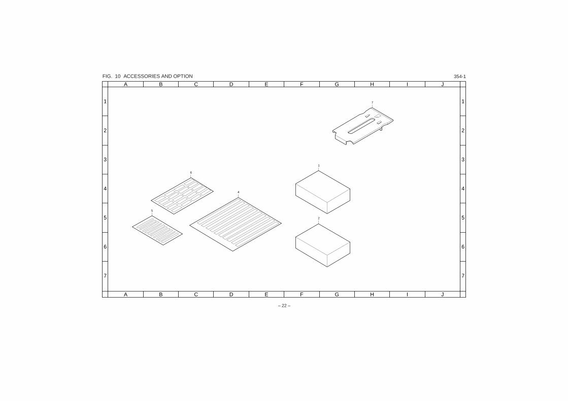
FIG. 10 ACCESSORIES AND OPTION
7
1
2
6
5
4
354-1
Part. No. DescriptionQuantity(230V)
Ref.No. Part. No. Description
Quantity(230V)
Ref.No.
354
– 23 –
• Parts with "•" are component parts or sub-assemblies of theassembly appearing immediately above them.
FIG. 10 ACCESSORIES AND OPTION
1 35482960 MEMORY BOARD FOR POINT SOURCE VI 30 (2M) 12 35482980 MEMORY BOARD FOR POINT SOURCE VI 30 (1M) 1
4 35405040 LABEL,LANGUAGE INSTRUCTION HANDBOOK 15 35405110 LABEL B,LANGUAGE INSTRUCTION HANDBOOK 16 35405050 SEAL,ONE-TOUCH 17 35306410 GUIDE,AUXILIARY 1
354-1
1
2
3
4
5
6
7
1
2
3
4
5
6
7
A B C D E F G H I J
A B C D E F G H I J
354
– 24 –
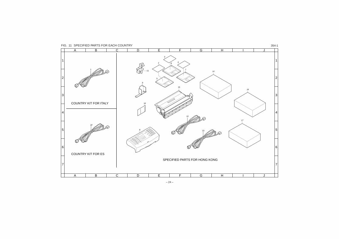
FIG. 11 SPECIFIED PARTS FOR EACH COUNTRY
6
5
7
2
3
4
1
12
138
10
9
11
15
COUNTRY KIT FOR ITALY
18
COUNTRY KIT FOR ES
SPECIFIED PARTS FOR HONG KONG
14
16
17
354-1
354
– 25 –
Part. No. DescriptionRef.No.
Quantity
IT ES MHK
FIG. 11 SPECIFIED PARTS FOR EACH COUNTRY
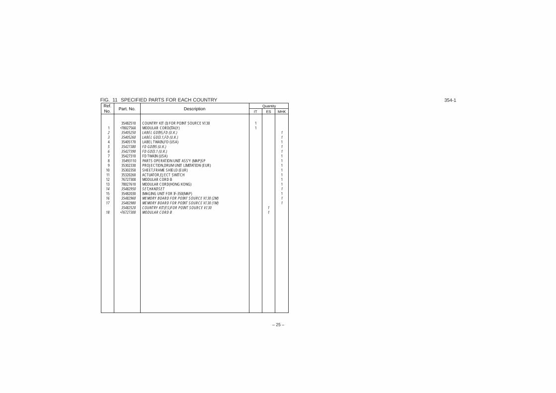
35482510 COUNTRY KIT (I) FOR POINT SOURCE VI 30 11 •78027560 MODULAR CORD(ITALY) 12 35405250 LABEL GDI95,FD (U.K.) 13 35405260 LABEL GDI3.1,FD (U.K.) 14 35405170 LABEL TWAIN,FD (USA) 15 35427380 FD GDI95 (U.K.) 16 35427390 FD GDI3.1 (U.K.) 17 35427310 FD TWAIN (USA) 18 35493110 PARTS OPERATION UNIT ASS’Y (MAP)SP 19 35302330 PROJECTION,DRUM UNIT LIMITATION (EUR) 1
10 35302350 SHEET,FRAME SHIELD (EUR) 111 35320260 ACTUATOR,EJECT SWITCH 112 76727300 MODULAR CORD B 113 78027610 MODULAR CORD(HONG KONG) 114 35482950 SET,HANDSET 115 35482030 IMAGING UNIT FOR IF-350(MAP) 116 35482960 MEMORY BOARD FOR POINT SOURCE VI 30 (2M) 117 35482980 MEMORY BOARD FOR POINT SOURCE VI 30 (1M) 1
35482520 COUNTRY KIT(ES)FOR POINT SOURCE VI 30 118 •76727300 MODULAR CORD B 1
354-1

– 24 –
354
Part. No. DescriptionQuantity(230V) Fig. No. Part. No. Description
Quantity(230V) Fig. No.
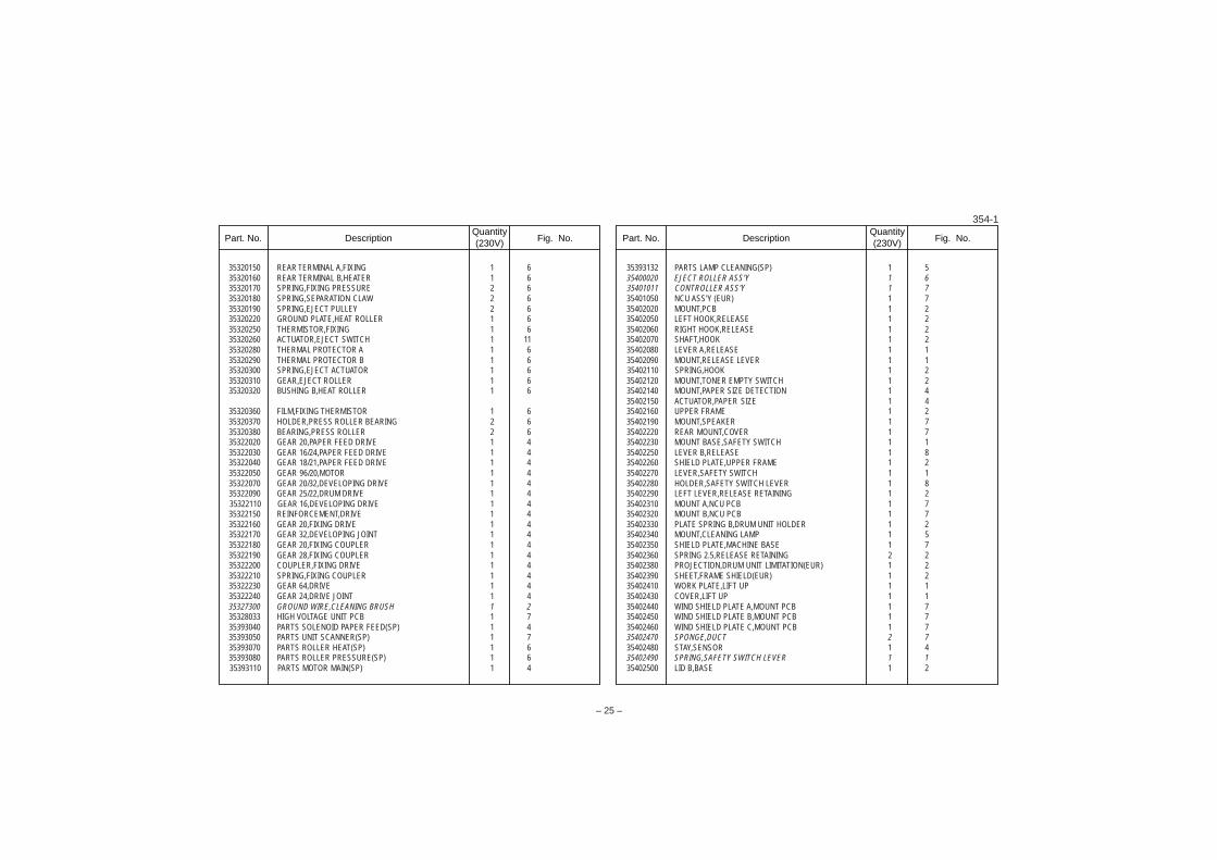
29717230 BUSHING 6,FEED BACK 1 829804160 PIN,ORIGINAL HOLDER 1 829806560 BUSHING 6 1 429806810 BUSHING,6 REGISTRATION 3 4, 829820420 PIN,BEARING 2 2, 6
35302030 TERMINAL,DRUM GROUND 1 435302040 TERMINAL,DEVELOPING BIAS 1 235302050 TERMINAL,SUB DEVELOPING BIAS 1 235302060 TERMINAL,TRANSFER MACHINE 1 235302070 TERMINAL,MAIN CHARGER 1 235302080 TERMINAL,GRID 1 235302090 TERMINAL,BRUSH 1 2
35302210 PLATE SPRING A,DRUM UNIT HOLDER 1 235302250 RIGHT LEVER,RELEASE RETAINING 1 235302260 GROUND PLATE,FRAME 1 235302290 GUIDE,DRUM SHAFT 1 235302330 PROJECTION,DRUM UNIT LIMITATION (EUR) 1 1135302350 SHEET,FRAME SHIELD (EUR) 1 1135302360 COVER,TERMINAL 1 235302400 TERMINAL BASE,MAIN CHARGER 1 2
35302420 LOWER SHEET,TERMINAL INSULATOR 1 235302430 SPRING,MAIN CHARGER 1 235302460 HOLDER,SAFETY SWITCH 1 235302470 STRAP A,MACHINE RELEASE 1 235302480 STRAP B,MACHINE RELEASE 1 2
35305060 LABEL, HIGH VOLTAGE CAUTION,L 1 235306010 PULLEY,PAPER FEED 1 435306020 SHAFT,PAPER FEED ROLLER 1 435306030 COLLAR,PAPER FEED 4 435306090 RACK,CURSOR 2 335306100 GEAR,CURSOR 1 335306110 SPRING,TRAY 1 335306120 SPRING,PAPER FEED CLUTCH 1 435306130 GEAR,PAPER FEED CLUTCH 1 435306140 BOSS,PAPER FEED CLUTCH 1 435306150 COLLAR,PAPER FEED CLUTCH 1 4
INDEX
35306160 HOLDER,PAD 1 435306170 PAD,PAPER FEED 1 4
35306190 PAD,TRAY 1 3
35306220 LOWER ROLLER,FEED 1 435306230 UPPER GEAR,FEED ROLLER 1 435306240 GEAR 20,PAPER FEED IDLE 1 435306250 BUSHING 4 2 435306260 ACTUATOR,PAPER FEED DETECTION 1 4
35306290 BUSHING 6,FEED 2 435306300 GROUND PLATE,PAPER FEED 1 4
35306330 GUIDE FILM,PAD 1 435306340 SPONGE,TRAY 1 335306350 SPRING,ACTUATOR 1 435306360 CUSHION,TRAY 2 235306380 SEAL,PAPER DUST DISPOSAL 1 5
35306410 GUIDE,AUXILIARY 1 1035306420 BRAKE,CURSOR 2 335306430 STOPPER,GEAR CURSOR 1 335306440 SPACER,PAD HOLDER 1 435312020 COVER,LSU 1 735312030 GROUND PLATE,LSU 1 735312040 CAP,LSU 1 735316020 BUSHING,TRANSFER 2 535316030 SPRING,TRANSFER 2 535316050 GUIDE,TRANSFER 1 5
35316110 PULLEY C,TRANSFER ROLLER 2 535316120 ROLLER,TRANSFER (METRIC) 1 535320030 BUSHING,HEAT ROLLER 1 635320071 SEPARATION CLAW,HEAT ROLLER 2 635320081 PULLEY,EJECT 2 635320090 GEAR,HEAT ROLLER 1 635320100 GEAR,FIXING IDLE 1 635320130 TERMINAL,THERMOSTAT 1 635320140 FRONT TERMINAL,FIXING 1 6
354-1
354
– 25 –
Part. No. DescriptionQuantity(230V) Fig. No. Part. No. Description
Quantity(230V) Fig. No.
35320150 REAR TERMINAL A,FIXING 1 635320160 REAR TERMINAL B,HEATER 1 635320170 SPRING,FIXING PRESSURE 2 635320180 SPRING,SEPARATION CLAW 2 635320190 SPRING,EJECT PULLEY 2 635320220 GROUND PLATE,HEAT ROLLER 1 635320250 THERMISTOR,FIXING 1 635320260 ACTUATOR,EJECT SWITCH 1 1135320280 THERMAL PROTECTOR A 1 635320290 THERMAL PROTECTOR B 1 635320300 SPRING,EJECT ACTUATOR 1 635320310 GEAR,EJECT ROLLER 1 635320320 BUSHING B,HEAT ROLLER 1 6
35320360 FILM,FIXING THERMISTOR 1 635320370 HOLDER,PRESS ROLLER BEARING 2 635320380 BEARING,PRESS ROLLER 2 635322020 GEAR 20,PAPER FEED DRIVE 1 435322030 GEAR 16/24,PAPER FEED DRIVE 1 435322040 GEAR 18/21,PAPER FEED DRIVE 1 435322050 GEAR 96/20,MOTOR 1 435322070 GEAR 20/32,DEVELOPING DRIVE 1 435322090 GEAR 25/22,DRUM DRIVE 1 435322110 GEAR 16,DEVELOPING DRIVE 1 435322150 REINFORCEMENT,DRIVE 1 435322160 GEAR 20,FIXING DRIVE 1 435322170 GEAR 32,DEVELOPING JOINT 1 435322180 GEAR 20,FIXING COUPLER 1 435322190 GEAR 28,FIXING COUPLER 1 435322200 COUPLER,FIXING DRIVE 1 435322210 SPRING,FIXING COUPLER 1 435322230 GEAR 64,DRIVE 1 435322240 GEAR 24,DRIVE JOINT 1 435327300 GROUND WIRE,CLEANING BRUSH 1 235328033 HIGH VOLTAGE UNIT PCB 1 735393040 PARTS SOLENOID PAPER FEED(SP) 1 435393050 PARTS UNIT SCANNER(SP) 1 735393070 PARTS ROLLER HEAT(SP) 1 635393080 PARTS ROLLER PRESSURE(SP) 1 635393110 PARTS MOTOR MAIN(SP) 1 4
35393132 PARTS LAMP CLEANING(SP) 1 535400020 EJECT ROLLER ASS’Y 1 635401011 CONTROLLER ASS’Y 1 735401050 NCU ASS’Y (EUR) 1 735402020 MOUNT,PCB 1 235402050 LEFT HOOK,RELEASE 1 235402060 RIGHT HOOK,RELEASE 1 235402070 SHAFT,HOOK 1 235402080 LEVER A,RELEASE 1 135402090 MOUNT,RELEASE LEVER 1 135402110 SPRING,HOOK 1 235402120 MOUNT,TONER EMPTY SWITCH 1 235402140 MOUNT,PAPER SIZE DETECTION 1 435402150 ACTUATOR,PAPER SIZE 1 435402160 UPPER FRAME 1 235402190 MOUNT,SPEAKER 1 735402220 REAR MOUNT,COVER 1 735402230 MOUNT BASE,SAFETY SWITCH 1 135402250 LEVER B,RELEASE 1 835402260 SHIELD PLATE,UPPER FRAME 1 235402270 LEVER,SAFETY SWITCH 1 135402280 HOLDER,SAFETY SWITCH LEVER 1 835402290 LEFT LEVER,RELEASE RETAINING 1 235402310 MOUNT A,NCU PCB 1 735402320 MOUNT B,NCU PCB 1 735402330 PLATE SPRING B,DRUM UNIT HOLDER 1 235402340 MOUNT,CLEANING LAMP 1 535402350 SHIELD PLATE,MACHINE BASE 1 735402360 SPRING 2.5,RELEASE RETAINING 2 235402380 PROJECTION,DRUM UNIT LIMITATION(EUR) 1 235402390 SHEET,FRAME SHIELD(EUR) 1 235402410 WORK PLATE,LIFT UP 1 135402430 COVER,LIFT UP 1 135402440 WIND SHIELD PLATE A,MOUNT PCB 1 735402450 WIND SHIELD PLATE B,MOUNT PCB 1 735402460 WIND SHIELD PLATE C,MOUNT PCB 1 735402470 SPONGE,DUCT 2 735402480 STAY,SENSOR 1 435402490 SPRING,SAFETY SWITCH LEVER 1 135402500 LID B,BASE 1 2
354-1
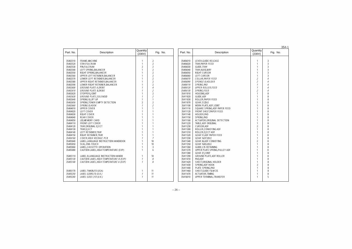
– 26 –
354
Part. No. DescriptionQuantity(230V) Fig. No. Part. No. Description
Quantity(230V) Fig. No.
35402510 FRAME,MACHINE 1 235402520 STAY,FULCRUM 1 235402530 PIN,FULCRUM 2 235402540 LEFT SPRING,BALANCER 1 235402550 RIGHT SPRING,BALANCER 1 235402560 UPPER LEFT RETAINER,BALANCER 1 235402570 LOWER LEFT RETAINER,BALANCER 1 235402580 UPPER RIGHT RETAINER,BALANCER 1 235402590 LOWER RIGHT RETAINER,BALANCER 1 235402600 GROUND PLATE A,DRIVE 1 435402610 GROUND PLATE B,DRIVE 1 235402620 STOPPER,JOINT 1 235402630 GROUND PLATE,SOLENOID 1 235402640 SPRING B,LIFT UP 1 135402650 SPRING,TONER EMPTY DETECTION 2 235402660 SPRING B,HOOK 1 235404010 UPPER COVER 1 135404020 LEFT COVER 1 135404030 RIGHT COVER 1 135404040 REAR COVER 1 135404050 LID,MEMORY CARD 1 135404110 FRONT LEFT COVER 1 135404120 TRAY,ORIGINAL EJECT 1 135404130 TRAY,EJECT 1 135404140 LEFT RETAINER,TRAY 1 135404150 RIGHT RETAINER,TRAY 1 135404160 COVER,HIGH VOLTAGE PCB 1 735405040 LABEL,LANGUAGE INSTRUCTION HANDBOOK 1 1035405050 SEAL,ONE-TOUCH 1 1035405060 LABEL,CASSETTE OPERATION 1 335405080 CAUTION LABEL,HIGH TEMPERATURE (EXP) 1 6
35405110 LABEL B,LANGUAGE INSTRUCTION HANDB 1 1035405130 CAUTION LABEL,HIGH TEMPERATURE B (EXP) 1 835405140 CAUTION LABEL,HIGH TEMPERATURE A (EXP) 1 8
35405170 LABEL TWAIN,FD (USA) 1 1135405250 LABEL GDI95,FD (U.K.) 1 1135405260 LABEL GDI3.1,FD (U.K.) 1 11
35406010 LEVER,GUIDE RELEASE 1 335406020 TRAY,PAPER FEED 1 335406030 GUIDE,TRAY 1 335406040 TRAY,AUXILIARY 1 335406050 RIGHT CURSOR 1 335406060 LEFT CURSOR 1 335406070 COLLAR,PAPER FEED 2 435406090 SPONGE B,HOLDER 2 435406110 SPRING,PAD 1 435406120 UPPER ROLLER,FEED 1 435406130 SPRING,FEED 2 435411010 HOUSING,ADF 1 835411020 GUIDE,ADF 1 835411030 ROLLER,PAPER FEED 1 835411070 GEAR 21,IDLE 1 835411100 WORK PLATE,ADF JOINT 1 835411110 SQUARE SPRING,ADF PAPER FEED 1 835411120 FRONT SHEET,PAPER FEED 1 835411140 HOLDER,PAD 1 835411150 SPRING,PAD 1 835411160 ACTUATOR,ORIGINAL DETECTION 1 835411220 TABLE,ADF ORIGINAL 1 835411230 CURSOR,ADF 2 835411300 ROLLER,CONVEYING ADF 1 835411310 ROLLER,EJECT ADF 1 835411320 GEAR 51,ADF PAPER FEED 1 835411330 GEAR 16/37,IDLE 1 835411340 GEAR 36,ADF CONVEYING 2 835411350 GEAR 16/65,IDLE 1 835411360 GUIDE,CIS RETAINING 1 835411370 UPPER PLATE SPRING,PULLEY ADF 1 835411380 GEAR 37,JOINT 1 835411390 GROUND PLATE,ADF ROLLER 1 835411410 PAD,ADF 1 835411420 SHEET,ORIGINAL HOLDER 1 835411430 SPRING,ADF HOOK 2 835411440 PLATE SPRING,PAD 1 835411460 SHEET,GUIDE FILM CIS 1 835411470 ACTUATOR,TIMING 1 835416010 UPPER TERMINAL,TRANSFER 1 5
354-1
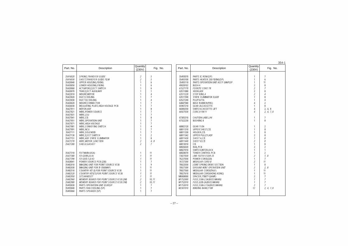
354
– 27 –
Part. No. DescriptionQuantity(230V) Fig. No. Part. No. Description
Quantity(230V) Fig. No.
35416020 SPRING,TRANSFER GUIDE 2 535416030 SHEET,TRANSFER GUIDE FILM 2 535420040 UPPER HOUSING,FIXING 1 635420050 LOWER HOUSING,FIXING 1 635420060 ACTUATOR,EJECT SWITCH 1 635420070 TRAY,EJECT AUXILIARY 1 135422010 MOUNT,MOTOR 1 435423020 DUCT,COOLING 1 735423030 DUCT B,COOLING 1 435426020 MOUNT,CONNECTOR 1 735426030 INSULATING PLATE,HIGH VOLTAGE PCB 1 735427011 MOTOR,ADF 1 835427021 WIRE,POWER SOURCE 1 735427031 WIRE,LSU 1 735427041 WIRE,CIS 1 835427051 WIRE,OPERATION UNIT 1 735427071 WIRE,HIGH VOLTAGE 1 735427081 WIRE,CONVEYING SWITCH 1 435427091 WIRE,NCU 1 735427111 WIRE,SOLENOID 1 735427130 WIRE,EJECT SWITCH 1 235427151 WIRE,ADF STATIC ELIMINATOR 1 835427270 WIRE,MOTOR JUNCTION 2 4, 835427280 SHIELD,GASKET 2 7
35427310 FD TWAIN (USA) 1 1135427380 FD GDI95,(U.K) 1 1135427390 FD GDI3.1,(U.K) 1 1135428041 POWER SOURCE PCB (230) 1 735482010 IMAGING UNIT FOR POINT SOURCE VI 30 1 935482030 IMAGING UNIT FOR IF-350(MAP) 1 1135482510 COUNTRY KIT (I) FOR POINT SOURCE VI 30 1 1135482520 COUNTRY KIT(ES)FOR POINT SOURCE VI 30 1 1135482950 SET,HANDSET 1 1135482960 MEMORY BOARD FOR POINT SOURCE VI 30 (2M) 2 10, 1135482980 MEMORY BOARD FOR POINT SOURCE VI 30 (1M) 2 10, 1135493030 PARTS OPERATION UNIT (EUR)SP 1 735493040 PARTS FAN COOLING (SP) 1 735493060 PARTS SPEAKER (SP) 1 7
35493070 PARTS IC ROM (SP) 1 735493100 PARTS HEATER 230 FIXING(SP) 1 635493110 PARTS OPERATION UNIT ASS’Y (MAP)SP 1 1149028102 BUSH 4 2 861527170 FERRITE CORE TR 2 763511080 HOOK,ADF 2 863511220 STOP RING,4 2 463511590 STATIC ELIMINATOR B,ADF 1 863527240 PI,GP1A71A 1 464847580 BASE RUBBER(PBS) 4 265907210 GEAR 20,CASSETTE 1 866006350 SWITCH,CASSETTE LIFT 4 2, 4, 866927030 CORE,9-19X11 4 2, 4, 7, 8
67305310 CAUTION LABEL,HV 1 767322230 BUSHING 8 1 8
68802120 GEAR 11/34 1 268811310 UPPER SHEET,CIS 1 868811330 HOLDER,CIS 1 868811342 UPPER PULLEY,ADF 2 868811430 SHEET A,CIS 1 868811440 SHEET B,CIS 2 868813010 CIS 1 868826020 RAIL,PCB 2 268827010 SWITCH,INTERLOCK 1 168828070 TONER CONTROL PCB 1 273827030 LINE FILTER ESDR-25 2 7, 876227030 POWER CORD(220) 1 776727300 MODULAR CORD B 2 1178022030 JOINT SPRING DRIVE SECTION 1 878027300 GROUND WIRE OPERATION UNIT 2 2, 878027560 MODULAR CORD(ITALY) 1 1178027610 MODULAR CORD(HONG KONG) 1 11
M0008000 SPACER,178877-2(AMP) 2 7M1752000 FUSE,S506-2.5A(BUSSMANN) 1 7M1752010 FUSE,GDB-2A(BUSSMANN) 1 7M1753010 FUSE,S506-3.15A(BUSSMANN) 2 7M2307010 BINDING BAND,T18R 12 2, 4, 7, 8
354-1
354
2-1-1
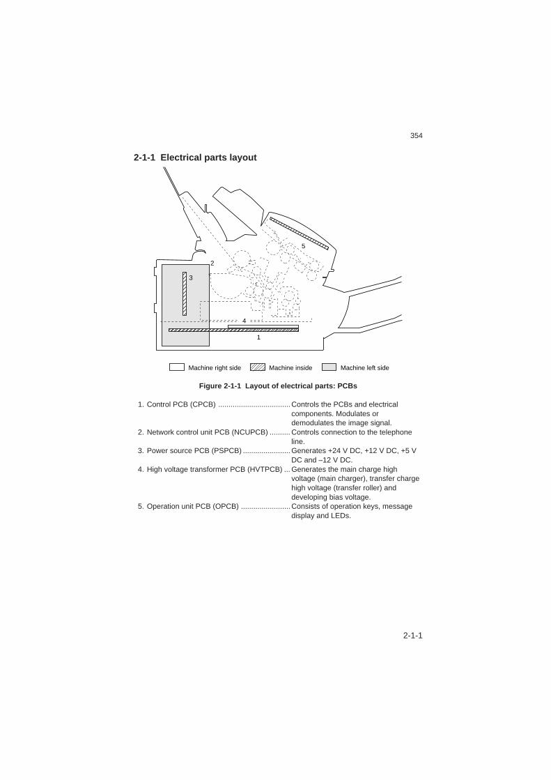
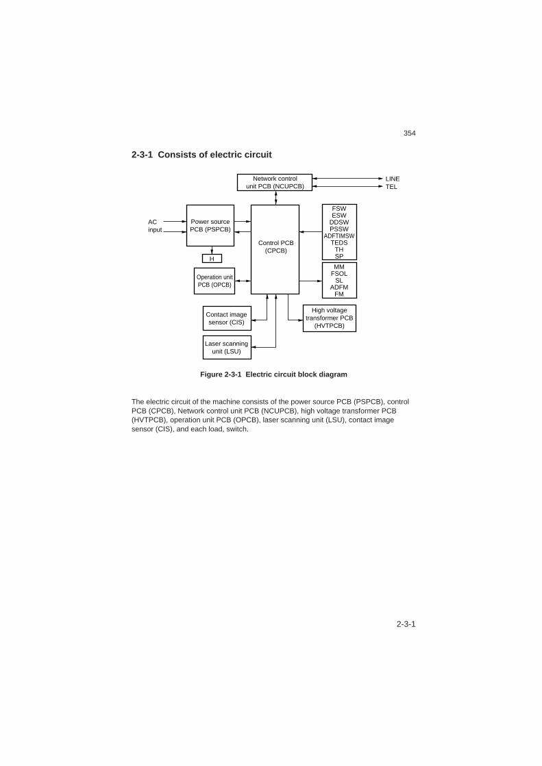
2-1-1 Electrical parts layout
5
2
3
4
1
Machine right side Machine inside Machine left side
Figure 2-1-1 Layout of electrical parts: PCBs
1. Control PCB (CPCB) ................................... Controls the PCBs and electricalcomponents. Modulates ordemodulates the image signal.
2. Network control unit PCB (NCUPCB) .......... Controls connection to the telephoneline.
3. Power source PCB (PSPCB) ....................... Generates +24 V DC, +12 V DC, +5 VDC and –12 V DC.
4. High voltage transformer PCB (HVTPCB) ... Generates the main charge highvoltage (main charger), transfer chargehigh voltage (transfer roller) anddeveloping bias voltage.
5. Operation unit PCB (OPCB) ........................Consists of operation keys, messagedisplay and LEDs.
354
2-1-2
##
2
36
4
1
5
98
7
Machine right side Machine inside Machine left side
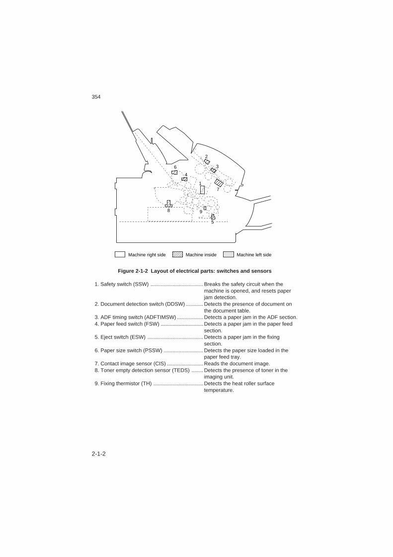
Figure 2-1-2 Layout of electrical parts: switches and sensors
1. Safety switch (SSW) ....................................Breaks the safety circuit when themachine is opened, and resets paperjam detection.
2. Document detection switch (DDSW) ............ Detects the presence of document onthe document table.
3. ADF timing switch (ADFTIMSW) ..................Detects a paper jam in the ADF section. 4. Paper feed switch (FSW) .............................Detects a paper jam in the paper feed
section. 5. Eject switch (ESW) ...................................... Detects a paper jam in the fixing
section. 6. Paper size switch (PSSW) ........................... Detects the paper size loaded in the
paper feed tray. 7. Contact image sensor (CIS) .........................Reads the document image. 8. Toner empty detection sensor (TEDS) ........ Detects the presence of toner in the
imaging unit. 9. Fixing thermistor (TH) ..................................Detects the heat roller surface
temperature.
354
2-1-3
1
23
4
Machine right side Machine inside Machine left side
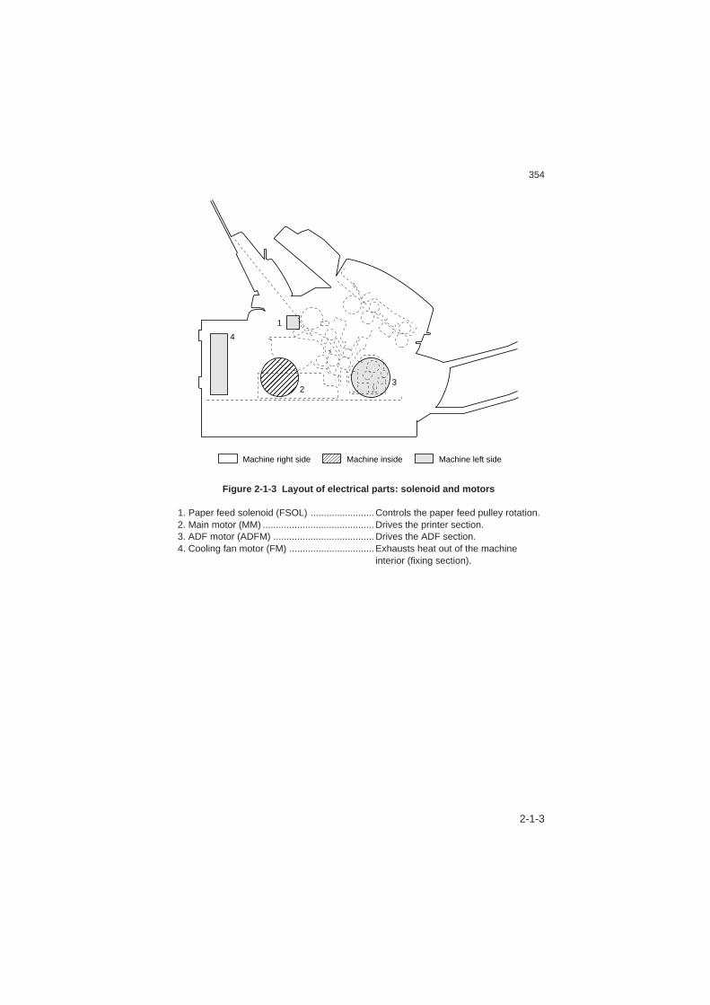
Figure 2-1-3 Layout of electrical parts: solenoid and motors
1. Paper feed solenoid (FSOL) ........................Controls the paper feed pulley rotation. 2. Main motor (MM) .......................................... Drives the printer section. 3. ADF motor (ADFM) ...................................... Drives the ADF section. 4. Cooling fan motor (FM) ................................Exhausts heat out of the machine
interior (fixing section).
354
2-1-4
61
2
3
4,5
Machine right side Machine inside Machine left side
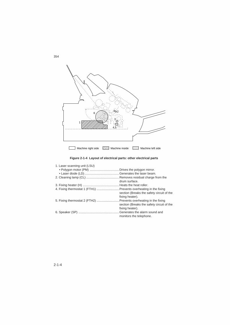
Figure 2-1-4 Layout of electrical parts: other electrical parts
1. Laser scanning unit (LSU)• Polygon motor (PM) ..................................Drives the polygon mirror.• Laser diode (LD) ........................................Generates the laser beam.
2. Cleaning lamp (CL) ...................................... Removes residual charge from thedrum surface.
3. Fixing heater (H) .......................................... Heats the heat roller. 4. Fixing thermostat 1 (FTH1) ..........................Prevents overheating in the fixing
section (Breaks the safety circuit of thefixing heater).
5. Fixing thermostat 2 (FTH2) ..........................Prevents overheating in the fixingsection (Breaks the safety circuit of thefixing heater).
6. Speaker (SP) ...............................................Generates the alarm sound andmonitors the telephone.
354
2-2-1
2-2-1 Paper jam detection
Paper jams are detected by the on and off timing of the switch equipped with the paperor document conveying path.
When a paper jam occurs, the error indicator lights up and a message of the paper jamis displayed on the message display. Also, for printing a PC, the status monitorindicating the paper jam is displayed on the computer screen too.
When a paper jam occurs, open the machine main body, then remove the jammedpaper. Also, if a document jam occurs, open the ADF cover and remove the jammeddocument or press the Stop/Reset key to eject the jammed document.
In order to reset for the paper jam, opening and closing the machine main body (turn offand on the safety switch).
A document jam is reset by turning on and off the document detection switch (DDSW) orADF timing switch (ADFTIMSW).In order to reset for the document paper jam, open the ADF cover and then remove thejammed document or press the Stop/Reset key and then eject the jammed document.
When the paper jam detected state is reset, the error indicator goes out and themessage in the message display goes out.
354
2-2-2
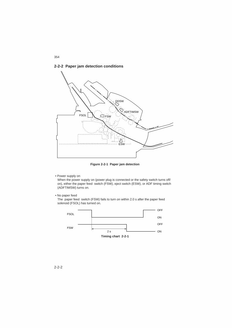
2-2-2 Paper jam detection conditions
DDSW
ADFTIMSWFSOL FSW
ESW
Figure 2-2-1 Paper jam detection
• Power supply onWhen the power supply on (power plug is connected or the safety switch turns off/on), either the paper feed switch (FSW), eject switch (ESW), or ADF timing switch(ADFTIMSW) turns on.
• No paper feedThe paper feed switch (FSW) fails to turn on within 2.0 s after the paper feedsolenoid (FSOL) has turned on.
FSOL
OFF
ON
OFF
ONFSW
2 s
Timing chart 2-2-1
354
2-2-3
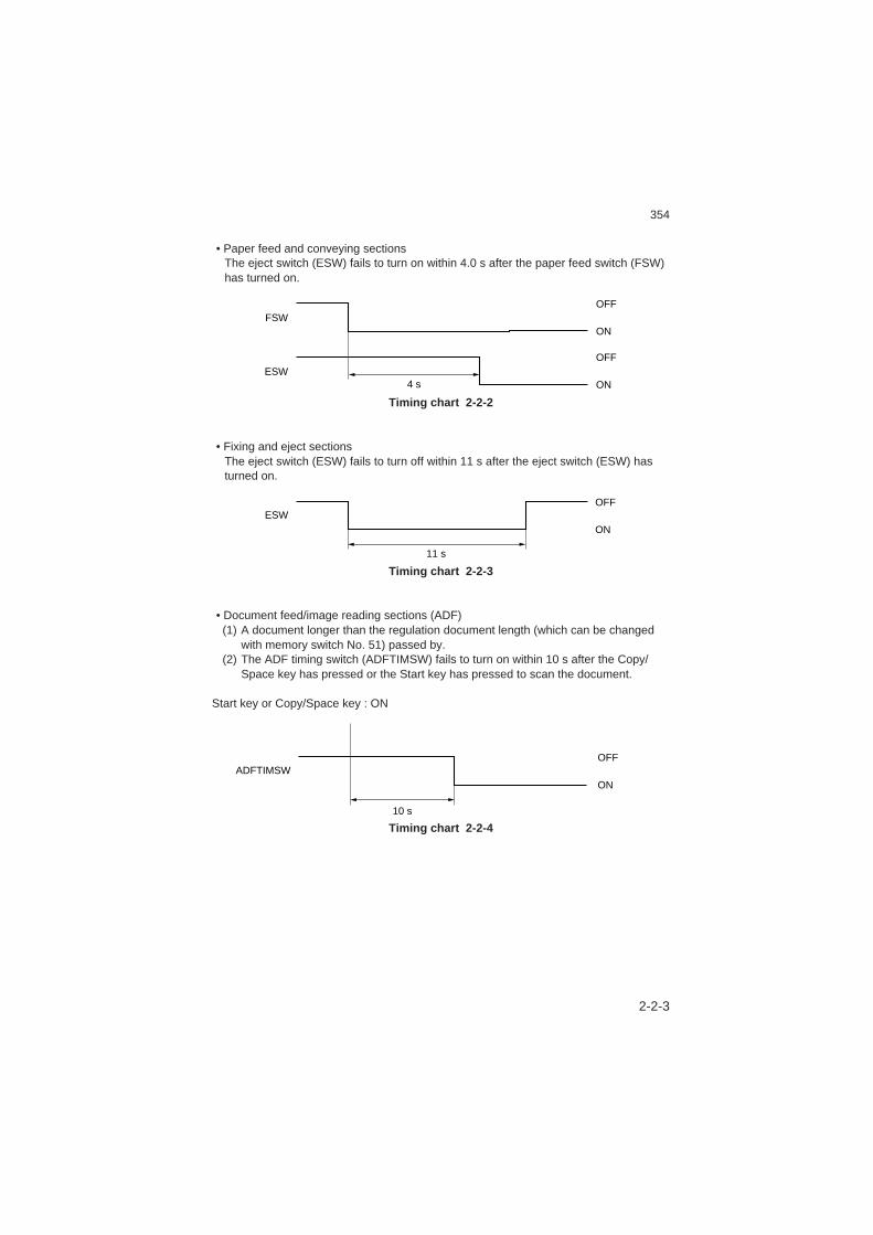
• Paper feed and conveying sectionsThe eject switch (ESW) fails to turn on within 4.0 s after the paper feed switch (FSW)has turned on.
ESW
OFF
ON
OFF
ON
FSW
4 s
Timing chart 2-2-2
• Fixing and eject sectionsThe eject switch (ESW) fails to turn off within 11 s after the eject switch (ESW) hasturned on.
ESWON
OFF
11 s
Timing chart 2-2-3
• Document feed/image reading sections (ADF)(1) A document longer than the regulation document length (which can be changed
with memory switch No. 51) passed by.(2) The ADF timing switch (ADFTIMSW) fails to turn on within 10 s after the Copy/
Space key has pressed or the Start key has pressed to scan the document.
Start key or Copy/Space key : ON
ADFTIMSW
OFF
ON
10 s
Timing chart 2-2-4
354
2-3-1
2-3-1 Consists of electric circuit
Network controlunit PCB (NCUPCB)
Control PCB(CPCB)
FSWESW
DDSWPSSW
ADFTIMSWTEDS
THSP
MMFSOL
SLADFM
FM
Contact imagesensor (CIS)
Laser scanningunit (LSU)
Power sourcePCB (PSPCB)
Operation unitPCB (OPCB)
H
High voltagetransformer PCB
(HVTPCB)
LINETEL
ACinput
Figure 2-3-1 Electric circuit block diagram
The electric circuit of the machine consists of the power source PCB (PSPCB), controlPCB (CPCB), Network control unit PCB (NCUPCB), high voltage transformer PCB(HVTPCB), operation unit PCB (OPCB), laser scanning unit (LSU), contact imagesensor (CIS), and each load, switch.
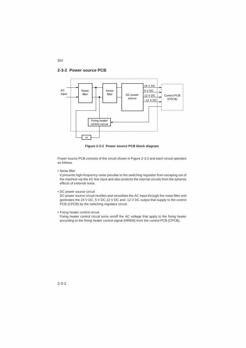
354
2-3-2
2-3-2 Power source PCB
ACinput
Noisefilter
Noisefilter DC power
source
Fixing heatercontrol circuit
Control PCB(CPCB)
24 V DC
5 V DC
12 V DC
–12 V DC
H
Figure 2-3-2 Power source PCB block diagram
Power source PCB consists of the circuit shown in Figure 2-3-2 and each circuit operatesas follows.
• Noise filterIt prevents high-frequency noise peculiar to the switching regulator from escaping out ofthe machine via the AC line input and also protects the internal circuits from the adverseeffects of external noise.
• DC power source circuitDC power source circuit rectifies and smoothes the AC input through the noise filter andgenerates the 24 V DC, 5 V DC,12 V DC and -12 V DC output that supply to the controlPCB (CPCB) by the switching regulator circuit.
• Fixing heater control circuitFixing heater control circuit turns on/off the AC voltage that apply to the fixing heateraccording to the fixing heater control signal (HREM) from the control PCB (CPCB).
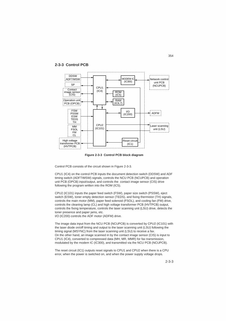
354
2-3-3
2-3-3 Control PCB
DDSWADFTIMSW
CPU1(IC4) ROM
(IC5)
RAM(IC6,7)
I/O(IC200)
MODEM IC(IC300)
Network controlunit PCB
(NCUPCB)
ADFM
Laser scanningunit (LSU)
CPU2(IC101)
FSWPSSWESWTEDS
TH
MMFSOL
FMCL
High voltagetransformer PCB
(HVTPCB)
Contactimage sensor
(CIS)
SP
Operation unitPCB (OPCB)
Reset circuit(IC1)
Figure 2-3-3 Control PCB block diagram
Control PCB consists of the circuit shown in Figure 2-3-3.
CPU1 (IC4) on the control PCB inputs the document detection switch (DDSW) and ADFtiming switch (ADFTIMSW) signals, controls the NCU PCB (NCUPCB) and operationunit PCB (OPCB) input/output, and controls the contact image sensor (CIS) drivefollowing the program written into the ROM (IC5).
CPU2 (IC101) inputs the paper feed switch (FSW), paper size switch (PSSW), ejectswitch (ESW), toner empty detection sensor (TEDS), and fixing thermistor (TH) signals,controls the main motor (MM), paper feed solenoid (FSOL), and cooling fan (FM) drive,controls the cleaning lamp (CL) and high voltage transformer PCB (HVTPCB) output,controls the fixing temperature, controls the laser scanning unit (LSU) drive, detects thetoner presence and paper jams, etc.I/O (IC200) controls the ADF motor (ADFM) drive.
The image data input from the NCU PCB (NCUPCB) is converted by CPU2 (IC101) withthe laser diode on/off timing and output to the laser scanning unit (LSU) following thetiming signal (MSYNC) from the laser scanning unit (LSU) to receive a fax.On the other hand, an image scanned in by the contact image sensor (CIS) is input toCPU1 (IC4), converted to compressed data (MH, MR, MMR) for fax transmission,modulated by the modem IC (IC300), and transmitted via the NCU PCB (NCUPCB).
The reset circuit (IC1) outputs reset signals to CPU1 and CPU2 when there is a CPUerror, when the power is switched on, and when the power supply voltage drops.
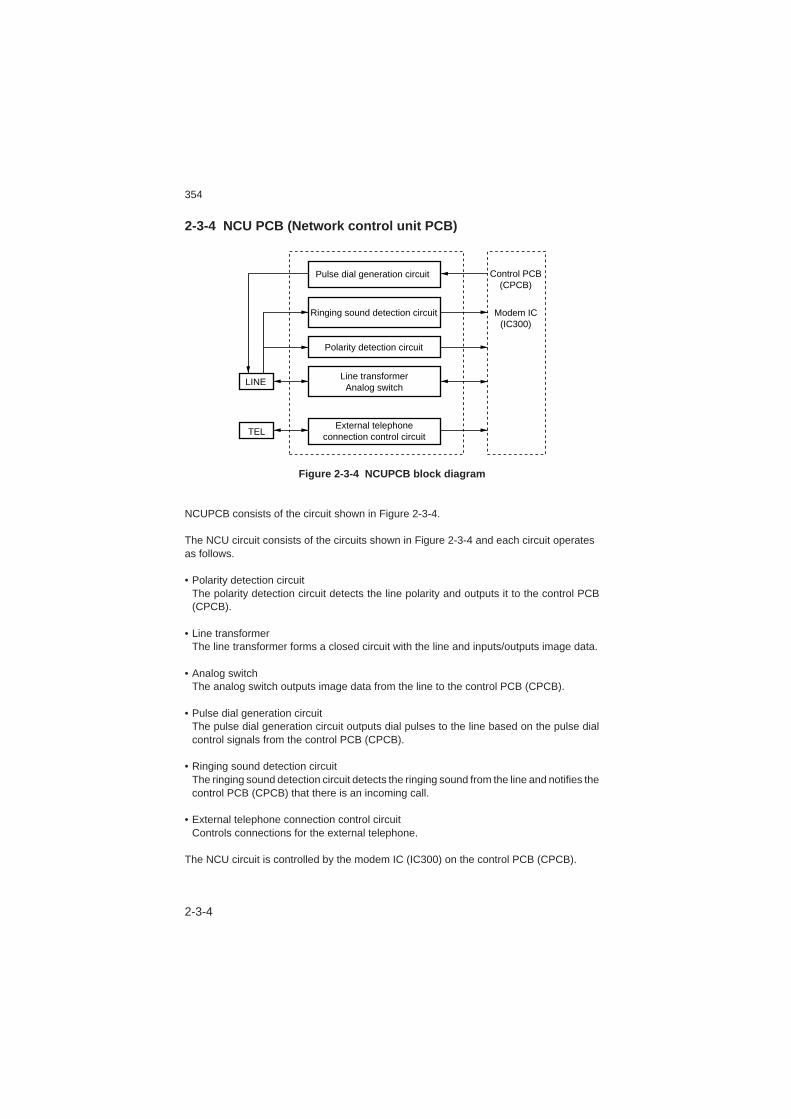
354
2-3-4
2-3-4 NCU PCB (Network control unit PCB)
Pulse dial generation circuit
Ringing sound detection circuit
Polarity detection circuit
External telephoneconnection control circuit
Line transformerAnalog switch
LINE
TEL
Control PCB(CPCB)
Modem IC(IC300)
Figure 2-3-4 NCUPCB block diagram
NCUPCB consists of the circuit shown in Figure 2-3-4.
The NCU circuit consists of the circuits shown in Figure 2-3-4 and each circuit operatesas follows.
• Polarity detection circuitThe polarity detection circuit detects the line polarity and outputs it to the control PCB(CPCB).
• Line transformerThe line transformer forms a closed circuit with the line and inputs/outputs image data.
• Analog switchThe analog switch outputs image data from the line to the control PCB (CPCB).
• Pulse dial generation circuitThe pulse dial generation circuit outputs dial pulses to the line based on the pulse dialcontrol signals from the control PCB (CPCB).
• Ringing sound detection circuitThe ringing sound detection circuit detects the ringing sound from the line and notifies thecontrol PCB (CPCB) that there is an incoming call.
• External telephone connection control circuitControls connections for the external telephone.
The NCU circuit is controlled by the modem IC (IC300) on the control PCB (CPCB).
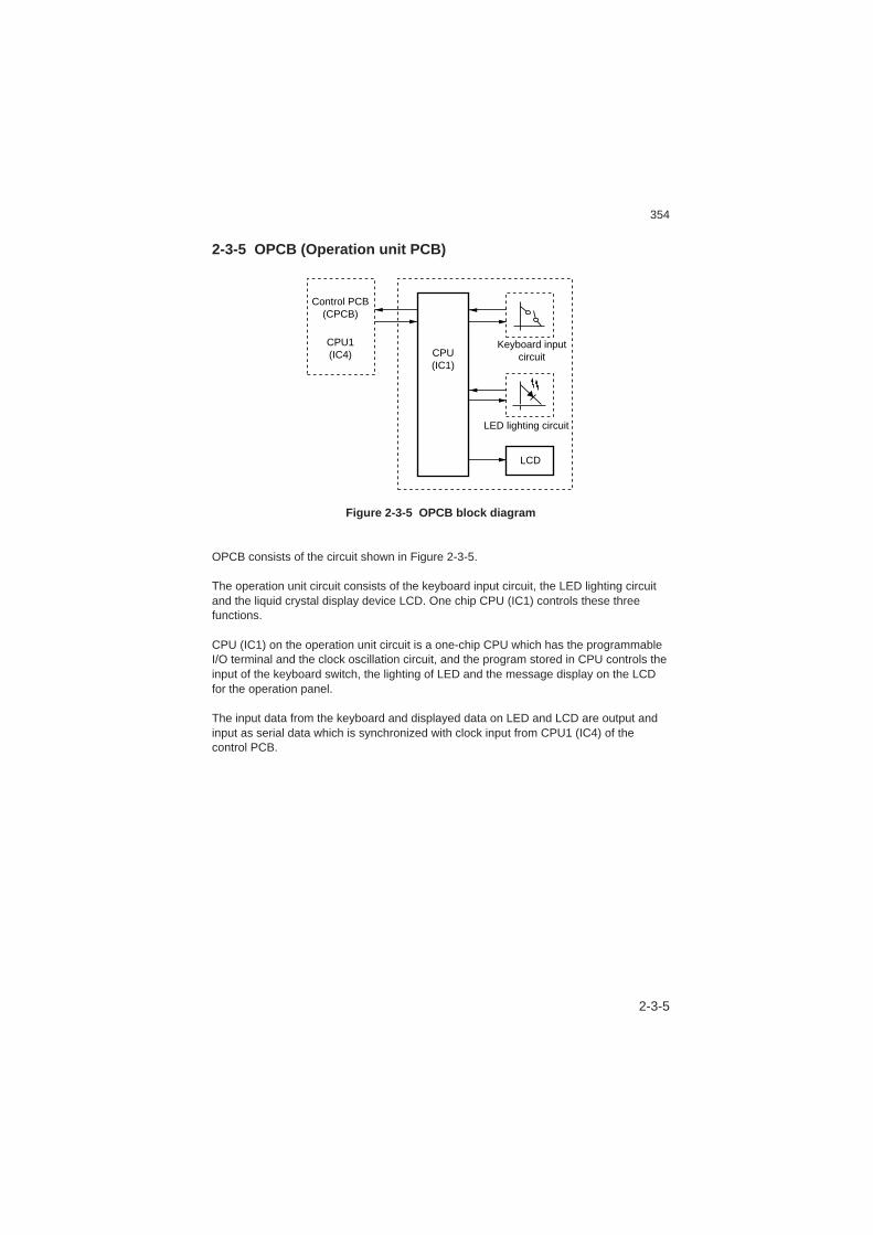
354
2-3-5
2-3-5 OPCB (Operation unit PCB)
Control PCB(CPCB)
CPU1(IC4) CPU
(IC1)
Keyboard inputcircuit
LED lighting circuit
LCD
Figure 2-3-5 OPCB block diagram
OPCB consists of the circuit shown in Figure 2-3-5.
The operation unit circuit consists of the keyboard input circuit, the LED lighting circuitand the liquid crystal display device LCD. One chip CPU (IC1) controls these threefunctions.
CPU (IC1) on the operation unit circuit is a one-chip CPU which has the programmableI/O terminal and the clock oscillation circuit, and the program stored in CPU controls theinput of the keyboard switch, the lighting of LED and the message display on the LCDfor the operation panel.
The input data from the keyboard and displayed data on LED and LCD are output andinput as serial data which is synchronized with clock input from CPU1 (IC4) of thecontrol PCB.

354
2-3-6
2-3-6 Communication Procedures
( 1 ) Outline
There are two different procedures available for facsimile transmission, one being usedfor communicating between our facsimiles and those of other manufacturers and theother being used for communication between our facsimiles.The facsimile machine has two standard modes, the internationally used and recog-nized G3 standard and our own standard.In the G3 mode, the facsimile machine automatically responds in the mode the othermachine is using.Our own standard can be selected and used only if the user selects it. If the othermachine does not use our standard, the facsimile automatically goes into the normal(G3) mode.

354
2-3-7
( 2 ) Communication Procedures
1. G3 transmission
Dial →
Next document(no mode change)
No document to send
Hung up
Originating machine(ours)
Receiving machine(other company's)
CNG
CED
(NSF, CSI) DIS
TSI, DCS
TCF
CFR
PIX,RTC
MPS
MCF
PIX,RTC
EOP
MCF
DCN
( ) Option signals
Figure 2-3-6 G3 procedure (transmission)
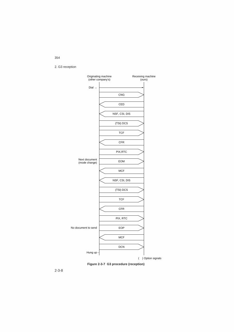
354
2-3-8
2. G3 reception
Dial →
Next document(mode change)
No document to send
Hung up
Originating machine(other company's)
Receiving machine(ours)
CNG
CED
NSF, CSI, DIS
(TSI) DCS
TCF
CFR
PIX,RTC
EOM
MCF
NSF, CSI, DIS
(TSI) DCS
TCF
CFR
PIX, RTC
EOP
MCF
DCN
( ) Option signals
Figure 2-3-7 G3 procedure (reception)
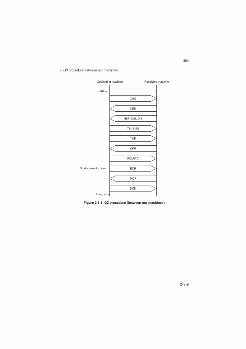
354
2-3-9
3. G3 procedure between our machines
Dial →
No document to send
Hung up
Originating machine Receiving machine
CNG
CED
NSF, CSI, DIS
TSI, NSS
TCF
CFR
PIX,RTC
EOP
MCF
DCN
Figure 2-3-8 G3 procedure (between our machines)
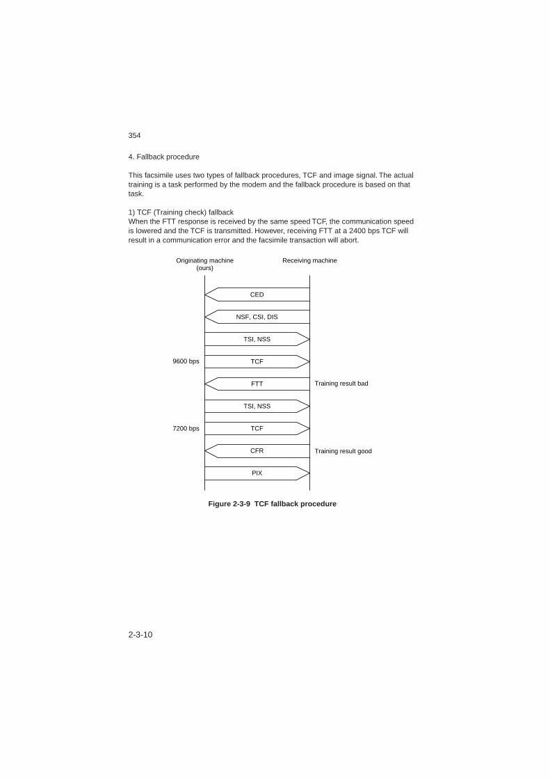
354
2-3-10
4. Fallback procedure
This facsimile uses two types of fallback procedures, TCF and image signal. The actualtraining is a task performed by the modem and the fallback procedure is based on thattask.
1) TCF (Training check) fallbackWhen the FTT response is received by the same speed TCF, the communication speedis lowered and the TCF is transmitted. However, receiving FTT at a 2400 bps TCF willresult in a communication error and the facsimile transaction will abort.
9600 bps
7200 bps
Training result bad
Training result good
Originating machine(ours)
Receiving machine
CED
NSF, CSI, DIS
TSI, NSS
TCF
FTT
TSI, NSS
TCF
CFR
PIX
Figure 2-3-9 TCF fallback procedure
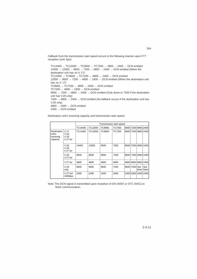
354
2-3-11
Fallback from the transmission start speed occurs in the following manner upon FTTreception (unit: bps):
TC14400 → TC12000 → TC9600 → TC7200 → 4800 → 2400 → DCN emitted14400 → 12000 → 9600 → 7200 → 4800 → 2400 → DCN emitted (When thedestination unit has no V. 17)TC12000 → TC9600 → TC7200 → 4800 → 2400 → DCN emitted12000 → 9600 → 7200 → 4800 → 2400 → DCN emitted (When the destination unithas no V. 17)TC9600 → TC7200 → 4800 → 2400 → DCN emittedTC7200 → 4800 → 2400 → DCN emitted9600 → 7200 → 4800 → 2400 → DCN emitted (Only down to 7200 if the destinationunit has V.29 only)7200 → 4800 → 2400 → DCN emitted (No fallback occurs if the destination unit hasV.29 only)4800 → 2400 → DCN emitted2400 → DCN emitted
Destination unit’s receiving capacity and transmission start speed
Transmission start speed
Destination unit's receiving capacity
V.17,V.33,V.29,V.27 ter
V.33,V.29,V.27 ter
V.29,V.27 ter
V.27 ter
TC9600 TC7200 9600 7200 4800 2400
V.27 ter/2400bps
V.29 only
TC9600
9600
9600
4800
2400
9600
TC7200
7200
7200
4800
2400
7200
TC14400 TC12000
TC14400
14400
9600
4800
2400
9600
TC12000
12000
9600
4800
2400
9600
9600
9600
9600
4800
2400
9600
7200
7200
7200
4800
2400
7200
4800
4800
4800
4800
2400
See Note
2400
2400
2400
2400
2400
See Note
Note: The DCN signal is transmitted upon reception of DIS (NSF) or DTC (NSC) tofinish communication.

354
2-3-12
2) Image signal fallbackWhen an RTN (Retraining Negative) is received in response to the image signal, thespeed is temporarily lowered. However if the speed cannot be lowered any further then,at that speed, the TCF fallback procedure will take place.
9600 bps
Next document
7200 bps
More than 15% of the total lines are error lines (it is possible to change in memory switch No.34 in service mode)
Originating machine(ours)
Receiving machine
PIX, RTC
MPS
RTN
TSI, NSS
TCF
CFR
PIX
Figure 2-3-10 Image signal fallback procedure

354
2-3-13
5. Aborting communications (Reset/Eject key)
Communications may be aborted by pressing the Reset/Eject key during facsimiletransmission. Figure 2-3-11 shows the procedure.
1) G3 procedure
Alarm
Originating machine Receiving machine
PIX
MSEG, RTC
EOP
MCF
DCN
Reset/Eject key ON →
Figure 2-3-11 G3 mode aborting procedure (transmission)
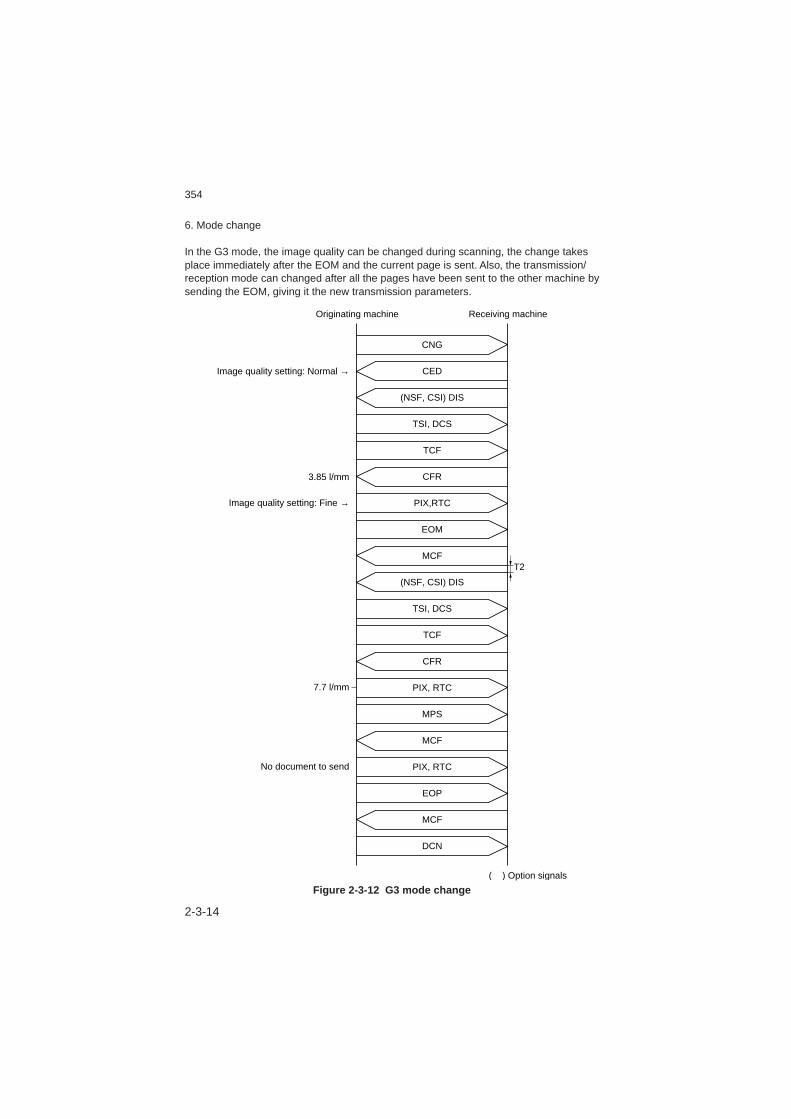
354
2-3-14
6. Mode change
In the G3 mode, the image quality can be changed during scanning, the change takesplace immediately after the EOM and the current page is sent. Also, the transmission/reception mode can changed after all the pages have been sent to the other machine bysending the EOM, giving it the new transmission parameters.
Image quality setting: Normal →
Image quality setting: Fine →
No document to send
3.85 l/mm
7.7 l/mm
Originating machine Receiving machine
CNG
CED
(NSF, CSI) DIS
TSI, DCS
TCF
CFR
PIX,RTC
EOM
MCF
(NSF, CSI) DIS
TSI, DCS
TCF
CFR
PIX, RTC
MPS
MCF
PIX, RTC
DCN
MCF
EOP
( ) Option signals
T2
Figure 2-3-12 G3 mode change
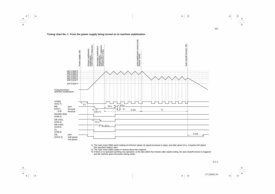
AA A
A
AA A
A
E
E E
E
E
E E
E
EA
EA
3-7 (354/E) A4
A B C D E F G H I J
A B C D E F G H I J
1
2
3
4
5
6
7
8
1
2
3
4
5
6
7
8
Timing chart No. 1 From the power supply being turned on to machine stabilization
3-7-1
354
1 s
0.6 s *1
181°C/358°F180°C/356°F179°C/354°F161°C/322°F160°C/320°F159°C/318°F
150°C/302°F
1.5 s
0.2 s
15 s 0.5 s
*2 2 min *3
5 min
H REM(CN1-7)
MC/DB1 REM(CN4-2)
DB CHG1(CN4-4)DB CHG2(CN4-5)CL(CN5-4)FM (CN14-2)
MM(CN6-1 – 6-6)
OFFForwardReverse
OFFHalf speedFull speed
Pow
er s
uppl
y: O
N
Prim
ary
stab
iliza
tion
tem
pera
ture
(150
°C/3
02°F
) de
tect
ion
*1: The main motor (MM) starts rotating at minimum speed, its speed increases in steps, and after about 0.6 s, it reaches full speed (the specified rotation rate).*2: The main motor (MM) rotates in reverse about two rotations.*3: If there is no operation (printing, key operation, or the like) within five minutes after stable ending, the auto shutoff function is triggered and the machine goes into power saving mode.
Sec
onda
ry s
tabi
lizat
ion
tem
pera
ture
(1
80°C
/356
°F)
dete
ctio
n(S
tabi
lizat
ion
ends
)
Initi
al s
tabi
lizat
ion
cont
rol e
nds
(Rea
dy m
ode)
Aut
o sh
utof
f fun
ctio
n: O
N
Fixing thermistor detection temperature
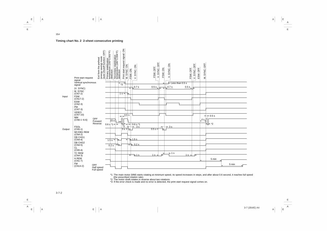
AA A A
A
AA A A
A
E
E E E
E
E
E E E
E
3-7 (354/E) A4
A B C D E F G H I J
A B C D E F G H I J
1
2
3
4
5
6
7
8
1
2
3
4
5
6
7
8
Timing chart No. 2 2-sheet consecutive printing
3-7-2
354
*1: The main motor (MM) starts rotating at minimum speed, its speed increases in steps, and after about 0.6 second, it reaches full speed (the prescribed rotation rate).*2: The motor shaft rotates in reverse about two rotations.*3: If the error check is made and no error is detected, the print start request signal comes on.
Print start requestsignalVertical synchronoussignal
(V. SYNC)M. SYNC(CN7-2)FSW(CN17-2)ESW(CN2-3)PM(CN7-3)VIDEO(CN7-10)MM(CN6-1~6-6) OFF
ForwardReverse
FSOL(CN5-1)
Input
OutputMC/DB1 REM(CN4-2)DB CHG1(CN4-4)DB CHG2(CN4-5)CL(CN5-4)TC REM(CN4-3)H REM(CN1-7)FM(CN14-2) OFF
Half speedFull speed
Exi
t for
m th
e pr
ehea
t (e
nerg
y sa
ving
) m
ode
(aut
o sh
utof
f fun
ctio
n: O
FF
)
Prim
ary
stab
iliza
tion
tem
pera
ture
(15
0°C
/302
°F)
dete
ctio
nS
econ
dary
sta
biliz
atio
n te
mpe
ratu
re (
180°
C/3
56°F
)de
tect
ion
Prin
t sta
rt r
eque
st s
igna
l: O
N
M. S
YN
C: O
FF
M. S
YN
C: O
N
FS
W: O
N
V. S
YN
C: O
N
ES
W: O
FF
V. S
YN
C: O
FF
FS
W: O
FF
V. S
YN
C: O
N
FS
W: O
N
V. S
YN
C: O
FF
FS
W: O
FF
*30.7 s 0.5 s 0.5 s0.7 s
Less than 0.5 s
1 s
0.6 s *1
1.5 s
1 s 1 s1 s
1 s
5 min
5 min
1.5 s
0.2 s 0.2 s
0.6 s *1
3 s 0.5 s
4 s
3 s 3 s
0.5 s
*2*2
0.5 s
15 s
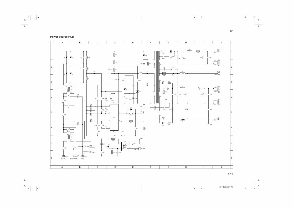
AA A
A
AA A
A
E
E E
E
E
E E
E
EA
EA
3-7 (354/E) A4
A B C D E F G H I J
A B C D E F G H I J
1
2
3
4
5
6
7
8
1
2
3
4
5
6
7
8
Power source PCB
3-7-3
354
D5
D12
R15
R30
R16
R24
D10
D7
D8
D4
Q1
F.B.
C15
R21
R20
R19
D2 D1
D3 D4
R14
R2C4
C14
R3
L4
R1
NOV1
R23
F4
F2
CN3-1AC LIVE AC NEUTRAL
CN2-1GND
H LIVE
H NEUTRAL
H REM
+5 V
CN4-1
CN6-1
CN1-10
CN5-1
C30
R26
3 R28
U2
R29 R27 C26
TH2
F1
C3
C2
C1
14
13
85
1611
1014
1513
129
23
+
+
L7
21
34
4
1
2
4
3
2
1
5
3
78
+C39
+
C13
C35 C36
D14
D11
D9
F.B.
F.B.
L5
L2
L5
L1
F3
C45
C23
C43
C22
C35
R18
R37
C16
C32
C44
C25
GNDR34
D13
C12C34
C3
C10
R10
R11
C8
C5
C6
C7
C11
R17R9R5
R7
R8
R12 R4
R34
R6
VR1
R33
Z2
TH1
+
C27+
C28+
C22+
C18+
C17+
C21+
C19R29 C33
+
C20
+
+24 V
CN1-1
PGCN1-3
+12 V
CN1-8
–12 V
CN1-9
NCCN1-2
+5 VCN1-4
NCCN1-5
NCCN1-7
SGCN1-6
U1
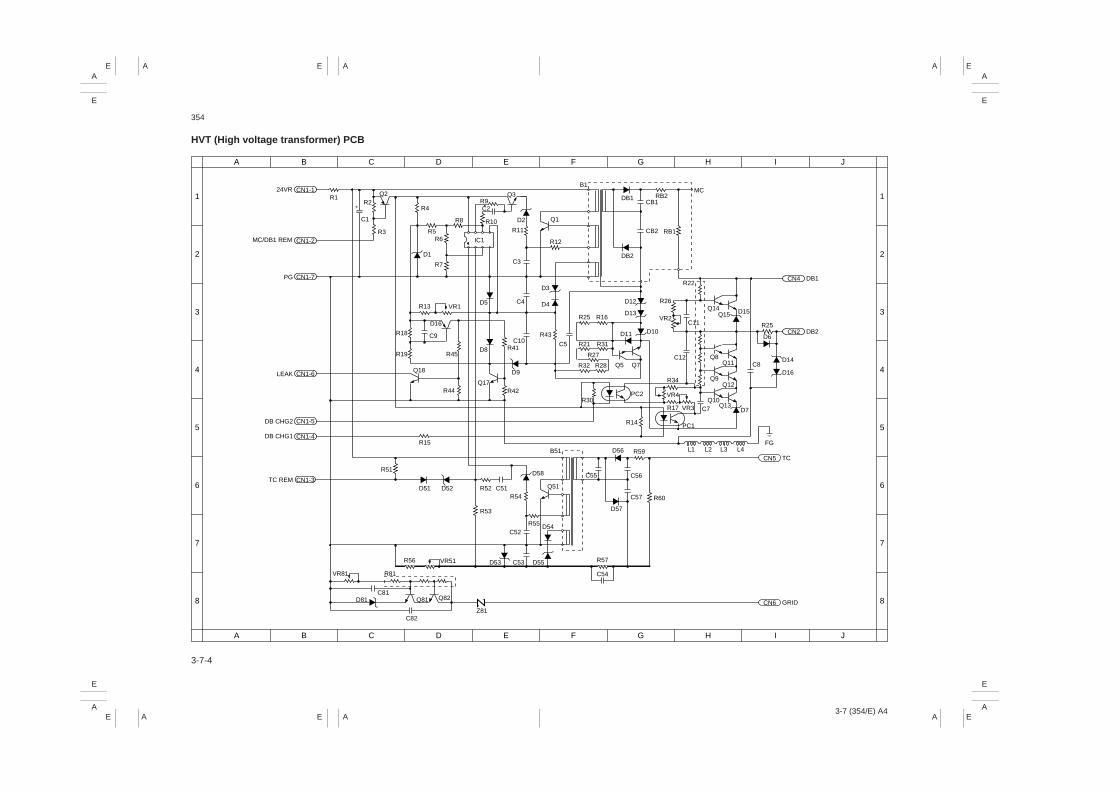
AA A A
A
AA A A
A
E
E E E
E
E
E E E
E
3-7 (354/E) A4
A B C D E F G H I J
A B C D E F G H I J
1
2
3
4
5
6
7
8
1
2
3
4
5
6
7
8
HVT (High voltage transformer) PCB
3-7-4
354
+
24VR
MC/DB1 REM
PG
CN1-1
CN1-2
CN1-7
LEAK CN1-6
DB CHG2 CN1-5
DB CHG1 CN1-4
TC REM CN1-3
R1R2
R4
R5
R8
C2R9
R12
Q3
Q1
B1
D2
C3
C4
C10
D9
R41
R42
D4D5
D8
Q17
D3
R10R11
R6
R7
D1
Q2
R3
C1
DB1CN4
DB2CN2
GRIDCN6
TCCN5
IC1
DB1
DB2
CB2
CB1RB2
MC
RB1
R13
R18
Q18
R19 R45
R44
R15
D51 D52 R52
R53
R54 R60
R59 L1 L2 L3 L4FG
R55 D54
D53 D55 R57
C54
C53
D58
D57
D56
C57
C55 C56
C51 Q51
B51
C52
R51
C9
VR1
D16
R56
R81
C81D81 Q81
Z81
Q82
C82
VR81
VR51
D7C7 Q13
Q12
Q11
Q10
Q9
Q8C8
R17
PC1
VR3
VR4
R34
C12
D10
D12
D13
D11
R26
R25
R22
VR2C11
D15
D14
D16
D6
Q15Q14
PC2
R14
R30
R32 R28
R16R25
R27
R21
R43
C5 R31
Q5 Q7

AA A
A
AA A
A
E
E E
E
E
E E
E
EA
EA
3-7 (354/E) A4
A B C D E F G H I J
A B C D E F G H I J
1
2
3
4
5
6
7
8
1
2
3
4
5
6
7
8
Control PCB 1/7
OPT_INT
/MODEM_DREQ
ACCINT
DMAINT
OPT_INT
ACCINT
DMAINT
/MPOEM_DREQ
/RNGDET/RNGDET
JP002
JP004
JP005
FGDG
AG
+12 V
+24 V
C002
R001
C004C005C006C007TP001
C003C001
–12 V
DG
AGAGAG
ONHOOK1
ONHOOK2
/OFFHOOK
ONHOOK1
ONHOOK2
/OFFHOOK
RDY
/RAMWE1/RAMWE0
/RAMOE1/RAMOE0
/HSYNC_OUTVDO0
SFTCLKNEWLINE
/HSYNC_OUTVDO0
SFTCLKNEWLINE
/OPT_MEM1
/OPT_MEM2
/OPT_MEM1
/OPT_MEM2
CLK_32M
CLK_16M
CLK_32M
/TELSEL
/PLSDIL
/KMUTE
/EARTH
/RXSEL
BUZZER
MONITOR
VOL0
VOL1
/DLYRESET
CN1
/TELSEL
/PLSDIL
/KMUTE
/EARTH
/RXSEL
BUZZER
A(0-23)
D(0-7)
/DLYRD
/WR
/MPOEMCS0
MONITOR
VOL0
VOL1
/DLYRESET
UNIT MAIN(CPU) UNIT MAIN(FAX CONTROLER_CA) UNIT MAIN(MODEM)
MAIN UNIT(RS232C)MAIN UNIT(GDI CONTROLER)MAIN UNIT(ENGINE CONTROLER)
D(0-7)
A(0-3)
/WR/DLYRD/IOCS
CLK_16M
OPT_INTOPT_INT
/DLYRESET
/WR
/IOCS
CLK_16M
EA(8-15)
ED(0-7)
ASB/EWR/ERD
VIDEO_CKVDO1ENCODEH_STROBE
GDI_INT
EA(8-15)CBSY0COMMAND0STATUS0SCCLK0SBSY0
CBSY0COMMAND0STATUS0SCCLK0SBSY0
READY0VSREQ0VSYNC0PRREQ0
SFTCLKVDO0NEWLINE
READY0VSREQ0VSYNC0PRREQ0
SFTCLKVDO0NEWLINE
CLK_32M
/HSYNC_OUT
GDICLK16M
CLK_32M
/HSYNC_OUT
GDICLK16M
/DLYRESET/DLYRESET
ED(0-7)
ASB/EWR/ERD
LED_ONLED_ON
/HEATER REM
VIDEO_CKVDO1
ENCODEH_STROBE
GDLINT
EA(8-15)
ED(0-7)
ASB/EWR/ERD
VIDEO_CKVDO1ENCODEH_STROBE
GDI_INT
/HSYNC_OUT
GDICLK16M
/DLYRESET
A(0-23)
D(0-7)
/RD
/WR
/DLYRD
/IOCS
/MODEMCS0
A(0-23)
D(0-7)
/RD
/WR
/DLYRESET
A(0-23)
D(0-7)
/RD
/WR
/DLYRD
/IOCS
/DLYRESET/DLYRESET
/TYLSEL
/PLSDIL
/KMUTE
/EARTH
/RXSEL
BUZZER
MONITOR
VOL0
VOL1
SBSY0
VSREQ0
READY0
MONITOR
VOL0
VOL1
SBSY0
VSREQ0
READY0
/TYLSEL
/PLSDIL
/KMUTE
/EARTH
/RXSEL
BUZZER
CLK_16M
RDY
/RNGDET
ONHOOK1
ONHOOK2
/OFFHOOK
/RNGDET
ONHOOK1
ONHOOK2
/OFFHOOK
/RAMWE1/RAMWE0
/RAMOE1/RAMOE0
/OPT_MEN1
/OPT_MEN2
/OPT_MEN1
/OPT_MEN2
LED_ONLED_ON
/MODEMCS0
CLK_16M
/MODEM_DREQ
/RAMOE0/RAMOE1/RAMWE0/RAMWE1
RDY
DMAINT
CBSY0PRREQ0COMMAND0VSYNC0SCCLK0
STATUS0SBSY0 STATUS0
SBSY0
CBSY0PRREQ0COMMAND0VSYNC0SCCLK0
ACCINT
1234567
24 VPG
+5 VSG
+12 V–12 V
H REM
+
++
+

AA A A
A
AA A A
A
E
E E E
E
E
E E E
E
3-7 (354/E) A4
A B C D E F G H I J
A B C D E F G H I J
1
2
3
4
5
6
7
8
1
2
3
4
5
6
7
8
Control PCB 2/7
+–
+5 V
8
6
5
DG
14
28
VBAT
R16
+5 V
C1
7 VCC
IC1
NCNCNCCND
OUT
NCCON
1234
DG
C3
VBAT
13 12
IC2F
DG
/MODEM_DREQ/MODEM_DREQ(5)
IC9A
4
DG
1 7DGC8
R1
+5 V
C2
DG
1
IC2A
2 R2
C4
DG
IC2B
3 4
IC2C
5 6
IC2D
9 8
IC2E
11 10R3
C5
DG
DLYRESET
D10..71
A10..231
DG
12111098765
IC5
A0
A3A4A5A6A7A8
A1A2
A9
A12A13A14A15A16A17
A10
A18
A11
272623254
282932
3031
A0A1A2A3A4A5A6A7A8A9A10A11A12A13A14A15A16A17A18
CEOE
2224
DG
C7
+5 V
13D0
D3D4D5
D1D2
D6
VPP
VCC
VSS
D7
14151718192021
D0D1D2D3D4D5D6D7
1
32
16
VBAT
152153154155
IC4
CLKINCLKOUT
PH12
RESET
RESR/WIRQVPRDYBE
EMU
INT0INT15INT16INT17
PC5PC4PC3PC2PC1PC0
RDYINPB6PB5PB4PB3PB2PB1PB0
PE7PE6PE5PE4PE3PE2PE1PE0
IA13IA12IA11IA10IA9IA8IA7IA6IA5IA4IA3IA2IA1IA0
ID7ID6ID5ID4ID3ID2ID1ID0
VPAVDANMI
ICSIRDIWR
SHRSACLK1ACLK2ASAMP
AINTEMP
ATAP
AVDD
AVSS
BACKUPMSEL
TEST1TEST0
156157
DG
+
125
122
126
158/DLYRESET9
AG
VBATC16
C17 C18
DG
DG
121416181101121141
VSSVSSVSSVSSVSSVSSVSS
VSS
20406080100120140160
VDDVDDVDDVDDVDDVDDVDD
VDD
102
58
59
9899
ROSC1
ROSC2
TXDSCLKRXD
108109
143142107103104105106
PF6PF5PF4PF3PF2PF1PF0
HVONPROTECT
EARTHLLED ON
PF5
KMUTELPLSDILLTELSELL
PA3PA2PA1PA0
54555657
/OPT MEM2/OT MEM1
5051
5352
PA7PA6PA5PA4
RUWR
ROMCSRAMCS
IOCSLCS0LCS1
23
54
678
PD3SPCLKBACKBREQ
22232425
A23A22A21A20
A23A22A21A20
26272829
A19A18A17A16
A19A18A17A16
42434445464748496263
A14A13A12A11A10A9A8A7A6
A15 A14A13A12A11A10A9A8A7A6A5
A15
D6D5D4D3D2D1D0
D7
64656667
6968
A5A4A3A2A1A0
A4A3A2A1A0
1312
14
1615
171819
D7D6D5D4D3D2D1D0
/RD/WR/ROMCS
95/S2
DDSW
VBAT
/DLYRESET(3, 4, 5, 6, 7)/DLYRESET
CLK_16M(4)
CLK 16M
DLTRESET
+5 V
DG
/VDOWN
PF6
IC31
53
24
ACCINT(4)OPT_INT(7)DMAINT(4)
DG
R6 R7 R8
DG DG3 5
DG
C9
+5 V
R51
/RNGDET(5) /RNGDET
IC9C
R5
ADFTIMSW
+5 V+5 V+5 V
R22 R23 R24 R25
+5 V
R26R27
R28
PRDY(2)
HRDY(2)/S1/HRDY
9697
133134135136137138139144145146147148149150
IA13IA12
IA10IA9IA8IA7IA6IA5IA4IA3IA2IA1IA0
110111112113114115116117151131132
129118119130
128
123124
ONHOOK2(5)
ONHOOK1(5)
/OFFHOOK(5)
AG
CN15123456789
10
SIGSG5 V
-12 VSGSI
SGCLK
LED REM24 V
SIG
SI
CIS CLK
R31
+5 V-12 V
+24 V
DG
AG
R29
C13
C12
VR1
+12 V
R30
R32
R33
36
IC10
C14
2
7
C15AG R34
AG-12 VD1
R35
DG
D2
TP1
TP2
R36
R37
C21
C20
DG
DG
+5 V
+5 V
R38
Q1
R39C19
DGLED_ON(3)
LED_ON
ONHOOK1ONHOOK2RL/PRDY
SBSY0VSREQ0BEADY0
SBSY0(3)VSREQ0(3)READY0(3)
MONITOR(5)VOL1(5)VOL0(5)
RDY(4)
MONITORVOL1VOL0
RDY
/UFFHOOK
/NM1
ACCINTDPT INTDMAINT
RXSELL
DG
9091929394
7071727374757677
10 11
8687
8584
8889
8382
159
30313233343536373839
7879
127
109876543
252421232
IC11
A0
A3A4A5A6A7A8
A1A2
A9
A12
A10A11
IA0
IA3IA4IA5IA6IA7IA8
IA1IA2
IA9
IA13
IA10IA12
262722
20
+5 V
CS1CS2WEOE
1918
15131211
1716
D7D6
D3D2D1D0
D5D4
28
14
VCC
GND
+5 V
C11
DG
C31 C32C30C29C28C27C26C25
DG
R40R41
X1
C22
C23DG
VBAT
L1
1 2
DG
Q3Z101
R43R42
D3
+5 V
Q2
DG DG
R46
R45
D4
/HRDY/PRDY
DGDGC33
DGC34
DGC35
DGC36
TXDSCLK OP
RXD
/OP_RES
DG
C37
DDSW
ADFTMSW
R55
+5 V
+5 V
1314
121110987654321
CN11
5V
DDSW
ADF TIMSW
SG
SG5V5VSGSIKCLKSOHSRENRSRENRESET
/EARTH(5)
/KMUTE(5)
/PLSDIL(5)
/TELSEL(5)
/RXSEL(5)
/EARTH
/KMUTE
/PLSDIL
/TELSEL
/RXSELTO MODEM CIRSUIT
BUZZER(5)
A(0-23)
D(0-7)
BUZZER
VCC
VSS 14
28
C6
VBAT
DG
D6D7
D5D4D3D2D1D0
1918171615131211
D7
D4D3D2D1D0
D6D5
A0A1A2A3A4A5A6A7A8A9A10A11A12A13A14
910
876543
252421232
261
IC7
A0
A3A4A5A6A7A8
A1A2
A9
A12A13A14
A10A11
20
2722 CS
OEWE
C38
910
876543
252421232
261
A0A1A2A3A4A5A6A7A8A9A10A11A12A13A14
D6D7
D5D4D3D2D1D0
1918171615131211
IC6
A0
A3A4A5A6A7A8
A1A2
D7
D4D3D2D1D0
D6D5
A9
A12A13A14
A10A11
20
2722 CS
OEWE
R4
VBAT
/RAMOE0(4)
/RAMOE1(4)
/RAMWE1(4)
/RAMWE0(4)
/RAMOE0
/RAMOE1
/RAMWE1
/RAMWE0
4
8
+5VGAE
IC8A
27
1
DG
R9 R10
+5 V
KUN13KUN14
KUN12KUN11KUN10
/OPT_MEM1(4)/OPT_MEM2(4)
/IOCS/RAMCS
/MODEMCS0 /IOCS(7)/MODEMCS0(5)
+5 V
+5 V
+5 V
R47 R48 R49 R50
R52
PF6
2
IC9B
6
DG
R11
R12R13
R14
R15
45
SW1
21
376
910
8
VBATDG
/DLYRD(5, 7)/DLYRD
/RD(4)/WR(4, 5, 7)
EARTHL
KMUTEL
PLSDILL
TELSELL
RXSELL
R18
R19
R20
R21
R17
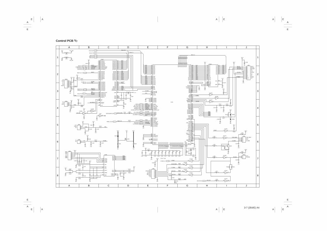
AA A
A
AA A
A
E
E E
E
E
E E
E
EA
EA
3-7 (354/E) A4
A B C D E F G H I J
A B C D E F G H I J
1
2
3
4
5
6
7
8
1
2
3
4
5
6
7
8
Control PCB 3/7
+24 V
12L110
EA (8-15)
ED (0-7)
ASB (6)/EWR (6)/ERD (6)
5758596061626364
12345678
4748495051525354
3637383945
4142
35
44
P20/S11P21/SO1P22/SCK1P23/STBP24/BUSYP25/SS10/SB0P26/SO0/SB1P27/SCK0
P30/TO0P31/TO1P32/TO2P33/T11P34/T12P35/PCLP36/BUZP37
P10/AN10P11/AN11P12/AN12P13/AN13P14/AN14P15/AN15P16/AN16P17/AN17
P00/IN T0/T10P01/IN TP1P02/IN TP2P03/IN TP3P04/XT1
X2X1
RESET
XT2
P40/AD0P41/AD1P42/AD2P43/AD3P44/AD4P45/AD5P46/AD6P47/AD7
P50/A8P51/A9
P52/A10P53/A11P54/A12P55/A13P56/A14P57/A15
P60P61P62P63
P64/RDP65/WR
P66/WAITP67/ASTB
VDD
VSSVSSVSS
AVDDAVREF
AVSS
1011121314151617
1819202122232526
2728293031323334
40
92443
5556
46
ED0ED1ED2ED3ED4ED5ED6ED7
EA8EA9EA10EA11EA12EA13EA14EA15
LEAK
/ERD/EWRWAITASB
EA18..151
ED10..71
IC100
2322212017161514
3130292827262524
121113
3435
988
139140142143
323938423349
24
14110
4748454643444041
949596
5356
123110
ED0ED1ED2ED3ED4ED5ED6ED7
EA8EA9EA10EA11EA12EA13EA14EA15
CLK 8M
INT1
VDO0SFTCLKNEW LINEVSYNC0PRREQ0/HSYNC OUT
CLK 32M
/DLYRESETWAIT
VDO1
ENCODEH STROBE
ED0ED1ED2ED3ED4ED5ED6ED7
EA8EA9EA10EA11EA12EA13EA14EA15
RDWRASB
CLK_8MCLK_8MINT1INT16
ADFM0ADFM1ADFM2ADFM3
VDO0SF TCLKNEW LINEVSYNC0PRREQ0/HSYNC_OUT
32MHZ16MHZRESETWAIT
PRREQ1VSYNC1VDO1VIDEO_CKENCODEH_STROBEPCL5/GDIN_VCLK0
CIINTPANELINTINT16CLR
DOTCLK0DOTCLK1
PORT1PORT2
SA0SA1SA2SA3SA4SA5SA6SA7SA8SA9
SA10SA11SA12
WFOE
FUOVHFUTHOPNSDHOPN
CS1CS2CS3CS4
LDENBS/H
LSUCLKSMON
SMLOCKHSYNC
SMRASMRBSMRASMRBMRM
SDHMASDHMBSDHMASDHMB
LMSTPTM
LPSCFOLOCK
TSMTNSC_CK
PSCFANHFANLGRIDHVTCHVCC
FPLOCKTPC
EXPC_CKAVRERR
EXPMRLSSRPRC
MMLOCKMMSI
TEST1
138137136135134133132131130129128125124
111112
81827167686970
74777692788075
636465667957585960
999810784
751068385103102101861046898971001059387
113
SA0SA1SA2SA3SA4SA5SA6SA7SA8SA9SA10SA11SA12
/LDEN
/HSYNCIC101/DLYRESET
CBSY0 (4)COMMAND0 (4)
STATUS0 (4)SCCLK0 (4)
SBSY0 (2, 4)SBSY0
INT1
FUTMPTNS
READY0VSREO0
GDI_INT/HSYNC
FUTMP (3)TNS (3)
READY0 (2)VSREO0 (2)
GDI_INT (6)
CBSY0COMMAND0STATUS0SCCLK0
+5 V
123456
SGFSW
5 V5 VSG
PSSW
+5 V+5 V
+5 V+5 V
+5 V
+5 V
FSW
PSSW
CN17
123
5 VSG
ESW
CN2
ESW
R104R100
C101
C101
+5 V +5 V
+24 V
D105
+5 V S5 V
+5 V
+24 V
123
+5 VTEDS
SG
CN3
12
THSG
CN18
123456
MMAMMA24 V24 VMMBMMB
CN6
TH FUTMP
C102
R107
R102
R105
R101
R106
R103
26
71CLK_8M
IC105B
53
IC5C
IC105A
TB
TEDS TNS
+5 V
+24 V
+5 V+5 V
+24 V
R109
C103
C104
C134C136 C135
C105
R108
R110
R132 R133
O104
81
1811
9
712
3
14
10
OUTAOUTAOUTBOUTB
RSA
VSAVSB
RETA
REFB
RSB
INAINAINBINB
TDATDB
GNDAGNDB
651716
213
415
MMAMMAMMBMMB
IC106
C132 C133
C142
C137R126
R130
R131
R127
R128
R124
R125
R129
S5 V
+5 V
C106 C107
C109
C108 VDO0 (4)SF TCLK (4)
NEW LINE (4)VSYNC0 (4)PRREQ0 (4)
/HSYNC_OUT (4, 6)
CLK_32M (4)
/DLYRESET (2)
VDO1 (6)
ENCODE (6)H_STROBE (6)
R111
R112
GDICLK16M (6)GDICLK16M
VIDEO_CK (6)VIDEO_CK
SX
INS
XO
UT
VS
SV
SS
VS
SV
SS
VS
SV
SS
VS
SV
SS
VS
SV
SS
VS
SV
SS
VC
CV
CC
VC
CV
CC
VC
CV
CC
VC
CV
CC
VC
C
51521271181089172625550361931144126109907361543718
18
C114
C113
C112C111 C115 C116 C117 C118 C119 C120 C121
37 54 144126109907361 R122
R123
C123
X100 C122
SD
7S
D6
SD
5S
D4
SD
3S
D2
SD
1S
D0
114115116117119120121122
SD
7S
D6
SD
5S
D4
SD
3S
D2
SD
1S
D0
109876543
25242123
2
20262722
A0A1A2A3A4A5A6A7A8A9A10A11A12
CS1CS2WEOE
D7D6D5D4D3D2D1D0
VCC
GND
1918171615131211
28
14
SD7SD6SD5SD4SD3SD2SD1SD0
IC102
1234567891011
MCLKMSYNCMSTARTPG24 VHSYNC5 VSGLDVIDEOVR
/M.CLK/M.SYNC/M.START
/H.SYNC
/VIDEO
CN7
+5 V
+5 V
+24 V
S5 V
S5 V
SD10..71
1234
FSOL REM24 V24 VCL REM
FSOL REM
CL REM
CN5
12
24 VFM REM
CN14
C124
C125
IC103B3 4
R113
+5 V
S5 V
R116
S5 V
+24 V
R114 R115
C126
C128
C127
R117
R119
R118
MMAMMBMMAMMB
D100B
D100A
32
21
IC103C
5 6/LDEN
C129
DG
DG
DGDG
AG
DG DG
DG
DG
DG
DG
DG
DG
DG
DG
DG DG
DG
DG DG
DG
DG
DG
DG DG
DG
DG
DG
DG
DG
DG
DG
DG
DG
DG
DG
DG
DG
DG
DG
C130
Q103
IC104A1 2
23
IC107A
76
IC107B
911
IC107C
1110
IC104E
98
IC104D
34
IC104B
1312
IC104F
56
IC104C
R120 R121
1614
IC107D
LED_ONLED_ON (2)
FM REM
H REM
MC/DB REM
TC REM
DB CHG1
DB CHG2
24 VMC/DB REM
TC REMDB CHG1DB CHG2
LEAKPG
H REM (1)
C113 - C121
1234567
CN4
C131
12
L100
+5 V_SW+5 V
12
L111
DG_SWDG
12
L112
12L101
12L102
+
IC103A1 2
C138 C141C139C140
+5 V
R141
C143
R140
R138
R139
R137
R136
LEAK
DG
12L106
12L107
12L108
12L105
12L109
12L104
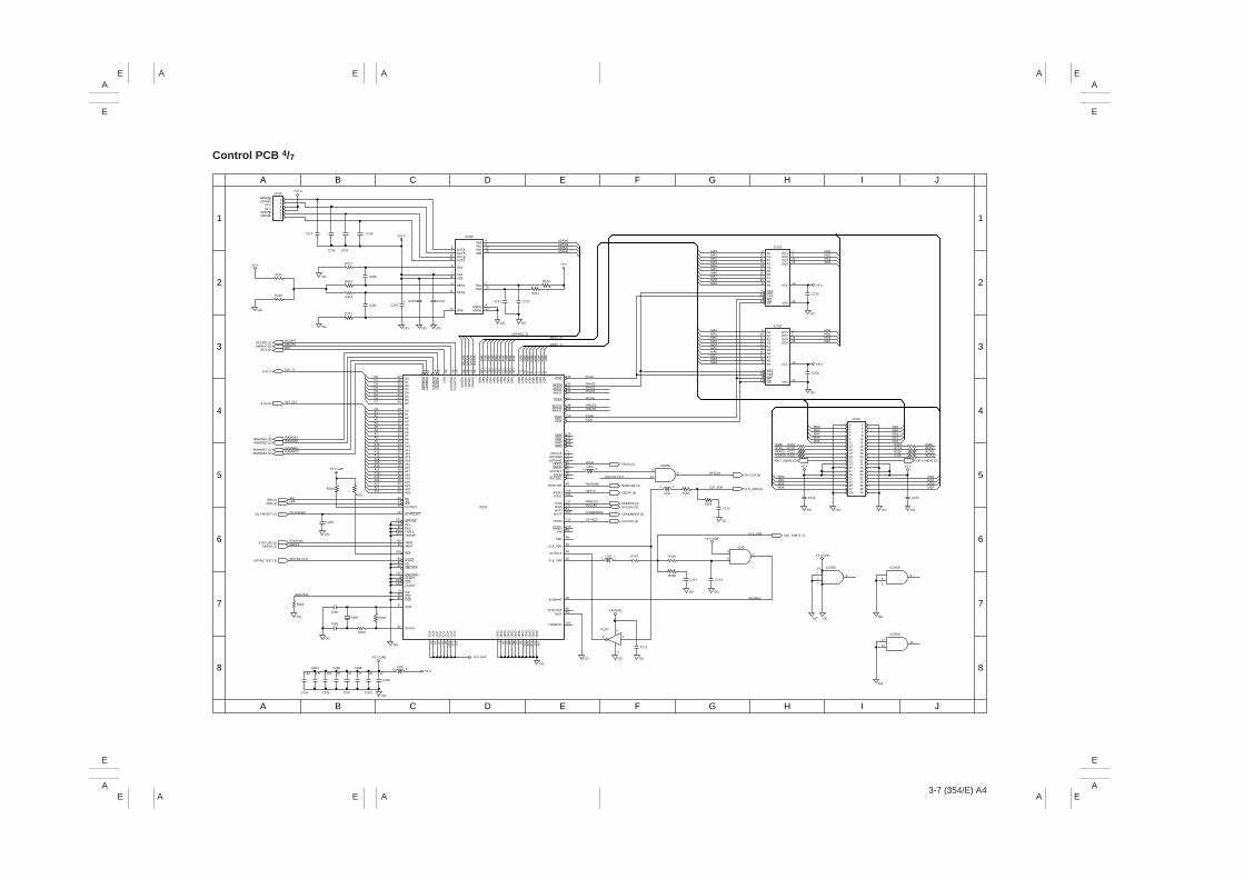
AA A A
A
AA A A
A
E
E E E
E
E
E E E
E
3-7 (354/E) A4
A B C D E F G H I J
A B C D E F G H I J
1
2
3
4
5
6
7
8
1
2
3
4
5
6
7
8
Control PCB 4/7
DG
5758596061626364
131415161719202122232425262728294546474849505152
535440
56
1019495
102103
9293
106
848269
1413
143140
798081
31
32
135
132133134
137
138139
1302
110112113114
7174777670758687
88
105104
11711191107
115
11678
89
33
34
35
38
8539
142
/ICAS
/IRAS0/IRAS1/IRAS2
/XCAS
/XRAS0/XRAS1
/DWR/DOE
D0D1D2D3D4D5D6D7
A0A1A2A3A4A5A6A7A8A9A10A11A12A13A14A15A16A17A18A19A20A21A22A23
RDWREXTRDY
DLYRESET
OPTCSLPELPEUTNFULTNEMP
JAM2JAM1
SAF
HSINCPDSMLOCK
ENCODEISTARTCLKCCDDT
INPCSLCSU
SXIN
SXOUT
D0D1D2D3D4D5D6D7
A0A1A2A3A4A5A6A7A8A9A10A11A12A13A14A15A16A17A18A19A20A21A22A23
ICAS
IRAS0IRAS1IRAS2
XCAS
XRAS0XRAS1
DWRDOE
MM0MM1MM2MM3
LSUCLKLDPWM0LDPWM1
VIDEOSMON
DOTSFTLDON
EXTDEC
NEWLINE
PSSUPSSL
HVMBIASHVTI
HVTP
HVEN
MMENFM
SSR
CLK_32M
DOTCLK
CLK_16M
IN16MHZ
TESTOUTTEST
CAMPON
+
DG
DG
+5 V GAE
R200
R201
C200
DG
R204
C201
X200
C202
R203
R202
DG
DG
DG
DG
DG
DG DG
DG
C214
C213C212
DG
DGDG DG
IC205A
DG
DG
DG
ACCINT (2)DMAINT (2)
RDY (2)
DG
DG
C221 C222
R211
R210
+5 V
DG
DG
+5 V
C215
IC201
DG
/RAMOE1 (2)/RAMOE0 (2)
/RAMWE1 (2)/RAMWE0 (2)
/RD (2)/WR (2)
STATUS0 (3)SBSY0 (3)
/DLYRESET (2)
/HSYNC OUT (3)
DG
C219 C220
+5 V +5 V
DG DG
CN16
DG DG
2+5 V
+5 V GAE+5 V GAE
112
C210
18
C209
73
C207
109
C205
144
C203
37
C208
90
C206
131
C204 L200
CN13
C227
C228 C229
C230
+24 V
+24 V IC208
+5 V
R215
R212
C226
C231 C225C223 C224
R213
R214
R217
R216
4567891011
1291281261251241231221211201199697989967666841424344
13612711810810083726555363011411311099073371812
MD
7M
D6
MD
5M
D4
MD
3M
D2
MD
1M
D0
MA
9M
A8
MA
7M
A6
MA
5M
A4
MA
3M
A2
MA
1M
A0
AD
FM
3A
DF
M2
AD
FM
1A
DF
M0
AC
CIN
TO
DM
AIN
TO
RD
Y
RA
MO
E1
RA
MO
E0
RA
MW
E1
RA
MW
E0
MD
7M
D6
MD
5M
D4
MD
3M
D2
MD
1M
D0
MA
9M
A8
MA
7M
A6
MA
5M
A4
MA
3M
A2
MA
1M
A0
AD
FM
3A
DF
M2
AD
FM
1A
DF
M0
GN
DG
ND
GN
DG
ND
GN
DG
ND
GN
DG
ND
GN
DG
ND
GN
DG
ND
VC
CV
CC
VC
CV
CC
VC
CV
CC
VC
CV
CC
ADFMAADFMA
24 V24 V
ADFMBADFMB
123456
651716
213
415
ADFM0ADFM2ADFM1ADFM3
81
1811
9
712
3
14
10
INAINAINBINB
TDATDB
GNDAGNDB
OUTAOUTAOUTBOUTB
RSA
VSAVSB
REFA
REFB
RSB
D (0-7)
A (0-23)
1 2
+5VGAE
2
3
5
4
IC207
C211
L202
1 2L203
1 2
L201 R205
R206
+5 V GAE
+5 V GAER207 R208
R209
ACCINTDMAINT RDY
D10..71
A10..231
/RAMOE1/RAMOE0
/RAMWE1/RAMWE0
/RD/WR
/DLYRESET
STATUS0SBSY0
/HSYNC OUT
SERVICE
ADFM10..31MA10..91
MD10..71
VDO0 (3)
IC200
NEWLINE (3)
SFTCLK (3)
/OPT_MEM1 (2) /OPT_MEM2 (2)
CLK_32M (3)CBSY0 (3)
PRREO0 (3)SCCLK0 (3)
COMMAND0 (3)
VSYNC0 (3)
VDO0
NEWLINE
CBSY0
PRREO0SCCLK0
COMMAND0
VSYNC0
/HSYNC OUT
9
108 SFTCLK
CLK_16M (2, 7)CLK_16M
IN16MHZ
CLK_32M
IC205C
5
63
14
23
7
1
IC8B
91011121415161718
5
423
322
122425
13
26
MD0MD1MD2MD3
MA0MA1MA2MA3MA4MA5MA6MA7MA8MA9
A0A1A2A3A4A5A6A7A8A9
RASCASWEOE
DQ1DQ2DQ3DQ4
VCC
VSS
+5 V
C216
IC2029
1011121415161718
5
423
322
122425
13
26
MD4MD5MD6MD7
MA0MA1MA2MA3MA4MA5MA6MA7MA8MA9
A0A1A2A3A4A5A6A7A8A9
RASCASWEOE
DO1DO2DO3DO4
VCC
VSS
MA0MA2MA4MA6MA8
MA1MA3MA5MA7MA9
MD0MD2MD4MD6
MD1MD3MD5MD7
/DOE/ICAS/IRAS2/XRAS0
R219R220R221R222
R223R224R225R226
/DWR/IRAS1/XCAS/XRAS1
13579111315171921232527293133353739
2468
10121416182022242628303234363840
IC205B
46
5
DG
IC205D
1211
13

AA A
A
AA A
A
E
E E
E
E
E E
E
EA
EA
3-7 (354/E) A4
A B C D E F G H I J
A B C D E F G H I J
1
2
3
4
5
6
7
8
1
2
3
4
5
6
7
8
Control PCB 5/7
+–
–+
–+
+–
DG
IC300
DG DG DG DG DG
DG
DG
AG
AG
AG AG AG
AG
DGAG
AGAGAG
AG AG AG AG
AGAG AG
AG
RXIN_N
AG
AG
AG
+5 V
+5 V
+5 V
+12 V
–12 V
+12 V
+5 V
+12 V
–12 V
AVCC
RXIN_N
ONHOOK2
/TELSEL/PLSDIL/KMUTE/EARTH
/TELSEL(2)/PLSDIL(2)/KMUTE(2)/EARTH(2) /RNGDET
ONHOOK1/RNGDET(2)
ONHOOK1(2)/RXSEL/RXSEL(2)
/OFFHOOKONHOOK2(2)
/OFFHOOK(2)
AVCC
–12 V
+5 V
C300 C301 C302 C303 C304
D(0-7)D(0-7)
A(0-6)A(0-6)
2627282930313233
17181920212223
373836353439
D0D1D2D3D4D5D6D7
A0A1A2A3A4A5A6
52
92541
/MODEMCS0/MODEMCS0(2)/MODEM_DREQ
/MODEM_DREQ(2)/WR/WR(2)
/DLYRD(2) /DLYRD
/DLYRESET(2) /DLYRESET
4349504551424454484746
SCCLKEOSBOSRDYSSCOUTSCINMC1CLKOUTMC0MC1MC2SD0SD1SD2SD3SD4SD5SD6SD7
SA0SA1SA2SA3SA4SA5SA6
SDTACKSINTRSCSSR/WSDSINT/MOT
DVDDDVDDDVDD
DGNDDGNDDGND
21
565553
6061
6258
63
575964
7645
16141513111210
2440
3
8
EXTALXTAL
HALT/NOP
VREFNAGNDRAGNDT
EYEXEYEY
TEST2TEST1
TXDCLKRXD
CDRTSCTS
RING
EYEX
R330
R331 R332 R333
R312
R315
R316
R305
R306
AVCC
C335
C334
CN12<SP>
SPSG
C332
R317
R304
AVCC
R302
R303
R318
IC302B IC302ALA6458M
IC304
R325
R324
R323
RXIN
R322
R320
R319
MODRXD
MODTXD
R321
C307
C306
C105
X300
C308AVCC
C310
C312C316
C320
VR300
C322
C326
2 1
8
3
3
1 8
6 4
52
67
5
C321
R313R314
C317C318
C313
C309
C311
C315
C319
C327
C325C324C323
CN10
C328
C176
C330
C331
R307
R308R310 R311
R309C329
C314
C199 IC301B
76
5
+
+
+
+
+
+
EYEY
1213
21
53
61110
9
X0IC303
X
Y
Z
VDD
VSS
VEE
14
15
4
16
8
7
X1
Y0Y1
12
Z0Z1
INHABC
EBS
TXA1TXA2
RXA1RXA2
AVDDVREFP
VCM
RESET
12345678910111213141516171819202122
ONHOOK1ONHOOK2TELSELPLSDILMODRXDRXSELMODTXDEARTHKMUTERNGDETOFFHOOKRXINN+12 V+12 VAGAG–12 V–12 V+5 V+5 VSGSG
R300
BUZZER(2)BUZZER
MONITOR(2)VOL0(2)VOL1(2)
MONITORVOL0VOL1MODRXD
MODRTD
DF11 · 22DP · 2DSA
+
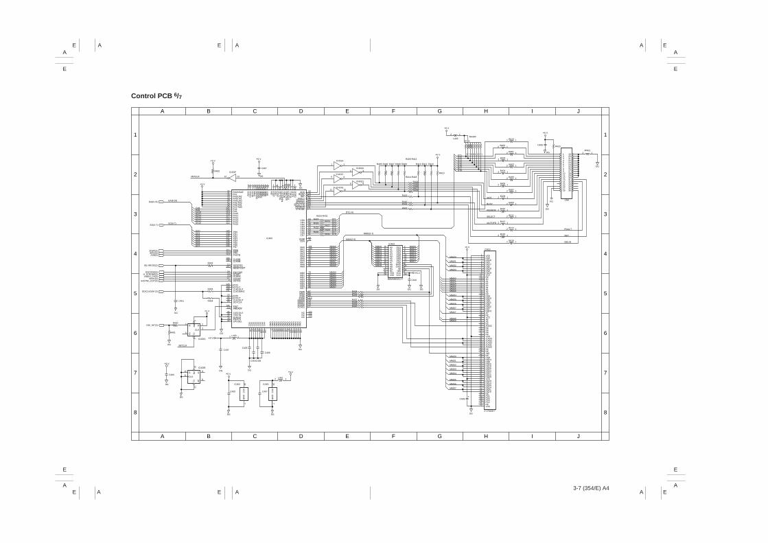
AA A A
A
AA A A
A
E
E E E
E
E
E E E
E
3-7 (354/E) A4
A B C D E F G H I J
A B C D E F G H I J
1
2
3
4
5
6
7
8
1
2
3
4
5
6
7
8
Control PCB 6/7
+
3231302928272625
121120119118117116115114
PA0/NSAFPA1PA2/LM2PA3/LM1PA4/LM0PA5/TM2PA6/TM1PA7/TM0PA8PA9PA10PA11PA12PA13PA14PA15
ACKBUSY
INITFAULT
SELECTAUTOFD
SELECTINPERRORSTROBE
595853515652505771
6867666564636261
DT1DT2DT3DT4DT5DT6DT7DT8
MMA0MMA1MMA2MMA3MMA4MMA5MMA6MMA7MMA8MMA9
MMA0MMA1MMA2MMA3MMA4MMA5MMA6MMA7MMA8MMA9
MMA0MMA1MMA2MMA3MMA4MMA5MMA6
MMD4
MMD5
MMD6
MMD7
MMA7
MMA8MMA9
MMD0
MMD1
MMD2
MMD3
MMD4
MMD5
MMD6
MMD7
MMD0MMD1MMD2MMD3MMD4MMD5MMD6MMD7
MMD0MMD1MMD2MMD3MMD4MMD5MMD6MMD7
MMD0
MMD1
MMD2
MMD3
6970
101112131617181920
96
211528
234524252627823722114
1011009998979695949392
7980818283848586
87888911374757677
123124125
CD0CD1CD2CD3CD4CD5CD6CD7
CDIRCEN
MA0MA1MA2MA3MA4MA5MA6MA7MA8MA9
MD0MD1MD2MD3MD4MD5MD6MD7
DWRIRASICASICASI
XRAS0XRAS1XCAS0XCAS1
NCNCNC
PD0PD1PD2PD3PD4PD5PD6PD7
PWRPRDPASTB
CLK8MCLK8M
RESETINRESETOUT
ENCODESTARTCLOCKCCDDTHSYNC
X1INX1OUTCLK1OUTCLK16MHZ
EA8EA9EA10EA11EA12EA13EA14EA15
EA(8-15)
ED(0-7)ED(0-7)
+5 V
+5 V
+5 V
+5 V
R433
C401
DG
R403
R404
R400
C400
R401
DG
DG
DG
DG
DG
DG DG DG
C410
DG
CN9
/FAULT
/INIT
/SELIN
DG
DG
FG
DG
DG
2
2 1
D
D
CLK
CLK
41
1013
PR
CL
PR
CL
IC402A
C402
L400
2 1L401
C403
C404C405
C406
IC402B
/INTCLR
3
9
8
5
12
11
Q
Q
Q
Q
+5 V
DG
147
VC
CG
ND
IC402
C400
+5 V
DG
147
VC
CG
ND
IC401
C407
6
+5 V+5 V
/EWR(3)/ERD(3)ASB(3)
ENCODE(3)H_STROBE(3)VIDEO_CK(3)
VDO1(3)/HSYNC_OUT(3)
/DLYRESE(2)
GDICLK16M (3)
GDI_INT(3)
EA(8-15)
ED0ED1ED2ED3ED4ED5ED6ED7
140139138137136135134133
14151617
2
128129130131
20212223
10613
4546474849
111112110
103104
12107
X2INX2OUTCLK2OUTDOTCLK
PINTPREADY
TESTOUTTESTINCLK121PGACSCPUSEL
R402C407
IC400
IC401F
DG
DG
IC401A
IC401C
IC401B
R405 R406 R407 R408 R409 R410 R411 R412
R413
10 5B413
RA400L403
12
12
B401 12
B403 12
B405 12
B407 12
B409 12
B411 12
B414 12
B416
CN19
12
B400 12
12
B402 12
B404 12
B406 12
B408 12
B410 12
B412 12
B415 12
12349876
R414-R418
R405-R412
R414R415R416R417R418
DT1DT2DT3DT4DT5DT6DT7DT8
/ACK
BUSY
PERROR
SELECT
/AUTOFD
R419
R420R421
R422
R434R435R436
R437R438R439R440
1
5
3
9
4
2
6
10
8
11
IC401D
R424-R431
DT(1-8)
MMD(0-7)
MMA(0-9)
R424
R426
R428
R430
R425
R427
R429
R431
IC401E
12 13/INTCLR
3451411421431198106744403842353439334143
LDO
NLD
PD
TN
FU
LLS
UC
LKS
MLO
CK
SM
ON
CS
TO
PE
NO
PT
CS
LP
SS
CP
EC
PS
ST
PE
T
SS
RM
MB
MM
AM
ME
ND
EN
SI
DE
NS
OB
IAS
HV
TP
HV
EN
HV
M
GN
DG
ND
GN
DG
ND
GN
DG
ND
GN
DG
ND
GN
DG
ND
GN
DG
ND
GN
DG
ND
GN
D
13212712210810510291787260553624191
VC
CV
CC
VC
CV
CC
VC
CV
CC
VC
CV
CC
1441261099073543718
+5 V
+5 V
+5 V
R423
JP401
123456789101112131415161718
192021222324252627282930313233343536
C408
IC403
M5M44800CJ-7
A0A1A2A3A4A5A6A7A8A9NCNCVSSVSS
DQ1DQ2DQ3DQ4DQ5DQ6DQ7DQ8RAS/CAS/
W/OE/
VCCVCC
123456789
101112131415161718192021222324252627282930313233343536373839404142434445464748495051525354555657585960616263646566676869707172
VSSDQ0DQ16DQ1DQ17DQ2DQ18DQ3DQ19VCCNCA0A1A2A3A4A5A6NCDQ4DQ20DQ5DQ21DQ6DQ22DQ7DQ23A7NCVCCA8A9NC/RAS2NCNCNCNCVSS/CAS0/CAS2/CAS3/CAS1/RAS0NCNC/WENCDQ8DQ24DQ9DQ25DQ10DQ26DQ11DQ27DQ12DQ28VCCDQ29DQ13DQ30DQ14DQ31DQ15NCPD1PD2PD3PD4NCVSS
DG
C409
2-176438-7
+5 V
+5 V
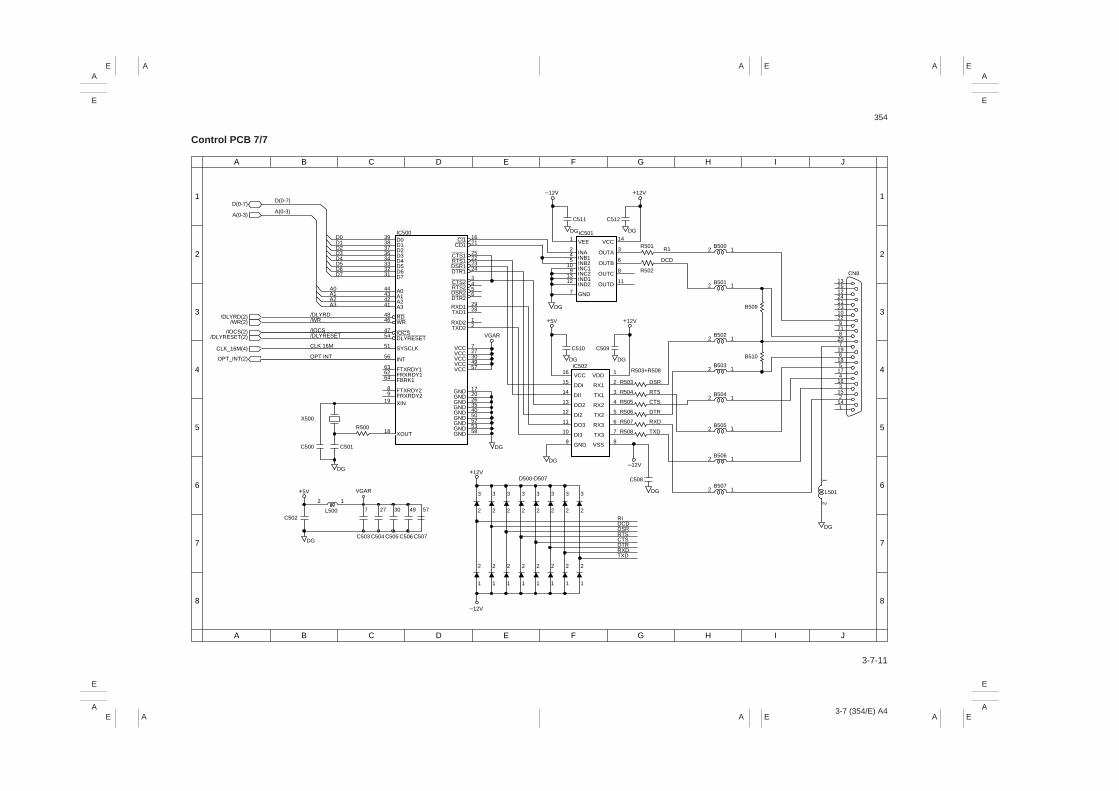
AA A
A
AA A
A
E
E E
E
E
E E
E
EA
EA
3-7 (354/E) A4
A B C D E F G H I J
A B C D E F G H I J
1
2
3
4
5
6
7
8
1
2
3
4
5
6
7
8
Control PCB 7/7
3-7-11
354
D(0-7)
A(0-3)
/DLYRD(2)/WR(2)
/IOCS(2)/DLYRESET(2)
CLK_16M(4)
OPT_INT(2)
D(0-7)
A(0-3)
D0D1D2D3D4D5D6D7
3938373634333231
1621
25222324
3456
2928
12
727304957
172026354050525358
A0A1A2A3
44434241
/DLYRD/WR
4846
/IOCS/DLYRESET
4754
CLK 16M 51
OPT INT 56
636264
89
19
18
IC500D0D1D2D3D4D5D6D7
CI1CD1
CTS1RTS1DSR1DTR1
CTS2RTS2DSR2DTR2
RXD1TXD1
RXD2TXD2
VCCVCCVCCVCCVCC
GNDGNDGNDGNDGNDGNDGNDGNDGND
A0A1A2A3
RDWR
IOCSDLYRESET
SYSCLK
INT
FTXRDY1FRXRDY1FBRK1
FTXRDY2FRXRDY2XIN
XOUTR500
C501
DG
DG
DG
DG
DG DG
DG
DG
DG
DG
DG
X500
C500
C502
+5V
+12V
VGAR
L500
2 1
7 27 30 49 57
C503 C504 C505 C506 C507
3
2
2
1
3
2
2
1
3
2
2
1
3
2
2
1
3
2
2
1
3
2
2
1
3
2
2
1
3
2
2
1
RIDCDDSRRTSCTSDTRRXDTXD
–12V
C508
16
15
14
13
12
11
10
9
1
2
3
4
5
6
7
8
R503
R504
R505
R506
R507
R508
DSR
RTS
CTS
DTR
RXD
TXD
VCC
DDI
DII
DO2
DI2
DO3
DI3
GND
VDD
RX1
TX1
RX2
TX2
RX3
TX3
VSS
R503+R508IC502
C509C510
C511 C512
+5V +12V
–12V +12V
VEE
INAINB1INB2INC1INC2IND1IND2
VCC
OUTA
OUTB
OUTC
OUTD
14
3
6
8
11
1
245
109
1312
7 GND
R501
R502
R1
DCD
13251224112310229218207196185174163152141
CN8
VGAR
B5002 1
2 1
2 1
2 1
2 1
2 1
2 1
2 1
12
B501
B509
B510
B502
B503
B504
B505
B506
B507L501
D500-D507
–12V
IC501
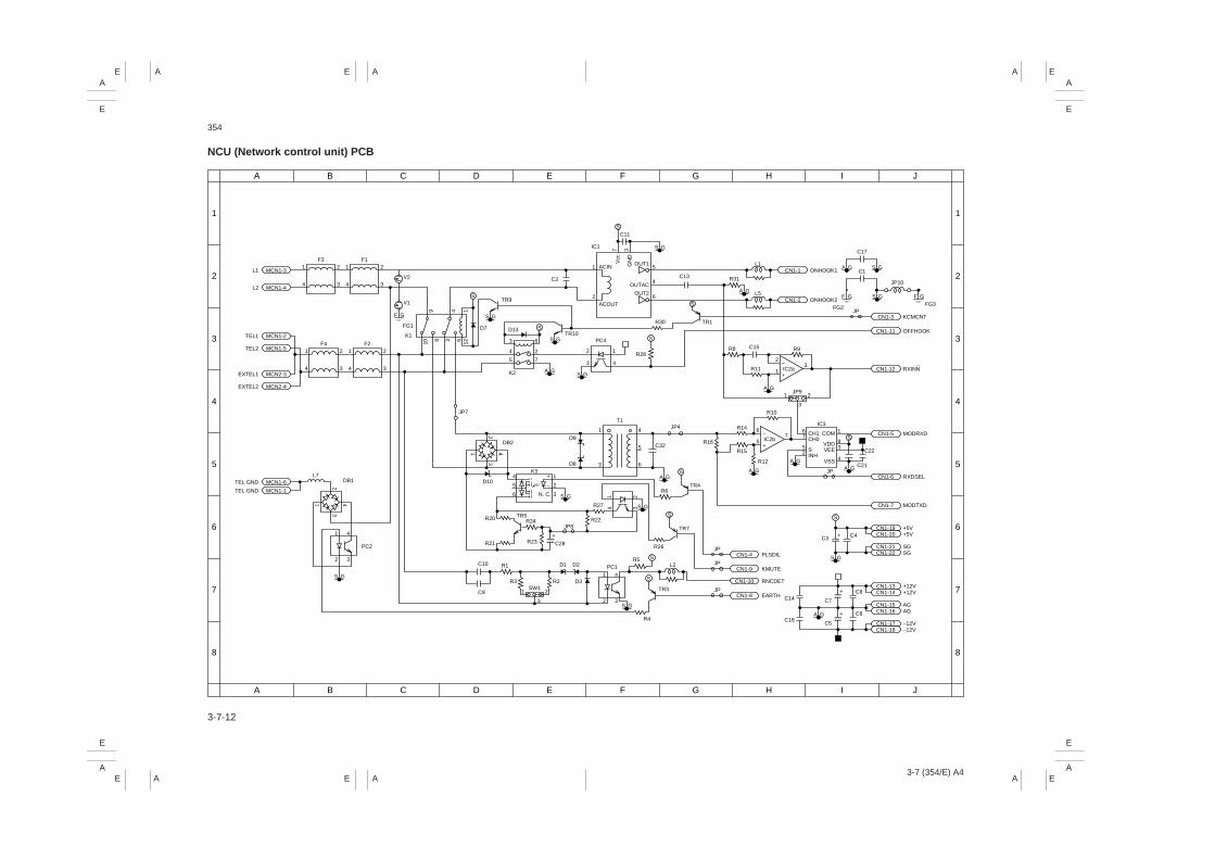
AA A A
A
AA A A
A
E
E E E
E
E
E E E
E
3-7 (354/E) A4
A B C D E F G H I J
A B C D E F G H I J
1
2
3
4
5
6
7
8
1
2
3
4
5
6
7
8
NCU (Network control unit) PCB
3-7-12
354
MCN1-3L11
4
2F3
3
MCN1-2TEL1
MCN1-5TEL2
MCN2-3EXTEL1
MCN2-4EXTEL2
MCN1-6TEL GND
MCN1-1TEL GND
MCN1-4L2
1
4
2F1
3V2
1
4
2F4
3
1
4
2F2
3
V1
FG1
K1
TR9
C2
C11
5ACIN
IC1
ACOUT
R28
R30
OUT1Vcc
GN
D
7 3
4
6
1
2
TR10PC4
D7 D13
2
74
1
3
2
K2
3
6
5
4
3N. C.
R20 R24TR5
R23
R22
R27
R6
R26
R5
R4
TR3
C28R21
R1
R3SW1
1 2
3
R2
D1 D2 PC1
D3
C10
C9
2
JP8
1
14
23
TR7
TR4
K3
–
+
2
4
D10
D9
D8 3
1
T1
6
4
C32
JP4
5
1
4
63
5
9 4 1123810 6
F G
F G F G
S
S
S
S
S
S
S
S
S G
S G
S G
A GS G
A G S G
A G
A G
A GA G
A G
S G
A G
A G
S G
S G
S G
S G
S G
OUT2
C13 R31
TR1
C15
R11
R16
R12
R14
R10
C22
C21
C4C3
R15
R8
L1
L5
OUTAC
CN1-1 ONHOOK1
CN1-2 ONHOOK2
C17
JP10
C1
FG3FG2
CN1-3 KCMCNT
CN1-11 OFFHOOK
CN1-12 RXINN–
+IC2a
IC3
CN1-5 MODRXD
CN1-6 RXDSEL
CN1-7 MODTXD
CN1-19 +5VCN1-20 +5V
CN1-21 SGCN1-22 SGCN1-4 PLSDIL
CN1-9 KMUTE
CN1-10 RNCDET
CN1-8 EARTH
R9
2
1
1 2
3
JP9
3
+
S
S
S
–
+IC2b
6
5
25
76
INHS
CH0CH1
4
38
1
VSS
VEEVDD
COM7
PC2
DB1
DB2
L7
1 4
2 3
1 4
2 3
CN1-13 +12VCN1-14 +12V
CN1-15 AGCN1-16 AG
CN1-17 –12VCN1-18 –12V
+
+
+
C8
C6C18
C14
C5
C7
JP
JP
JP
JP
JP
L2
32
41
JP7
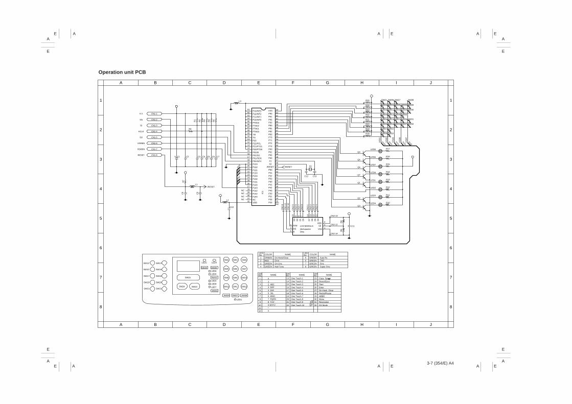
AA A
A
AA A
A
E
E E
E
E
E E
E
EA
EA
3-7 (354/E) A4
A B C D E F G H I J
A B C D E F G H I J
1
2
3
4
5
6
7
8
1
2
3
4
5
6
7
8
Operation unit PCB
SW28SW17SW09
SW21
SW22
SW24
SW25
SW27
SW26
SW11
SW12
SW13
SW30
SW31
SW32SW14
SW19
SW15
SW16
SW20
R15
KS
07
KS
06
KS
03
KS
02
R17
R16
R14
R13
R12
R11
R25
R24
R23
R22
R21
R20
R19
R18
Q6
LED6Q5
KS
01
P120
P121
P122
P131
P132
LED5Q4
LED7X1
Q1
LED8
LED3
LED2
LED1
Q7
Q2
C13C12
R10LED4Q3
R9
C11
R8VSS
CN2-12
CN2-13
V0VDD
16character
LCD MODULE 32
1
14 13 12 11
Reset/Eject
Copy Space
28 Redial/Pause
CN2-14
5
COLOR
GREEN Auto Rx.TAD 6
3130
EnterOn-Hook Clear
Start
8
7 FineGREEN
GREEN
2726
25
Super Fine
24
23
29 ABBR
ResolutionMenu
RX Mode 32
L3
/RESET
IC1
C7C6C5
KS06KS01
KS07
/RESET
NCNC
R6
R1
R2
R3
R4
R5
5 V
SG
SI
KCLK
SO
HSREN
RSREN
RESET
CN1-1
CN1-2
CN1-3
CN1-4
CN1-5
CN1-6
CN1-7
CN1-8C1+ C2 C4C3
L1R
7
C9
C8
546
GREENError
LEDNo.
LEDNo.
SWNo.
SWNo.
SWNo.
On-Hook/Clear 1
COLOR
2
6
SW4SW3SW2
C10
L2
On-Line
4
3
GREEN
GREEN
181716
1514
13
5 4
3 2
1 012 ABC3 DEF4 GHI5 JKL6 MNO7 PQRS8 TUV9 WXYZ*#
NAME NAME NAME
NAME NAME
10 22
212019
9 8 7
1211
Half-Tone
SW32
SW31
SW12SW11
SW10SW9
LED8
LED4
LED7
LED5
LED6
SW1
SW8
SW7SW6SW5SW26
LED1
SW28SW27SW29
SW24
SW29SW18 SW23SW10
SW22SW21
SW20SW19
SW18SW17
SW16SW15
SW23
SW25
2line
KS03KS02
0102030405060708091011121314151617181920212223242526272829303132
GREENREDLED3SW14SW13
SW08
SW01
SW02
SW03
SW04
SW05
SW06
SW07
LED2
SW30
One Touch 6
RS
10 9 8 7
One Touch 1
One Touch 2One Touch 3
One Touch 4One Touch 5
One Touch 9One Touch 8One Touch 7
One Touch 10D
7D
6D
5D
4
D3
D2
D1
D0
E
R/W
P13/INT3P12/INT2P11/INT1P10/INT0PTH03PTH02PTH01PTH00TI0TI1P23P22/PCLP21/PTO1P20/PTO0P03/SIP02/SOP01//SCKP00/INT4P123P122P121P120P133P132P131P130P143P142P142P140NCVDD
VSSP90P91P92P93P80P81P82P83P70P71P72P73P60P61P62P63X1X2
/RESETP50P51P52P53P40P41P42P43P30P31P32P33
6463626160595857565554535251504948474645444342414039383736353433NC
CN
2-1
CN
2-2
CN
2-3
CN
2-4
CN
2-9
CN
2-11
CN
2-10
CN
2-5
CN
2-6
CN
2-7
CN
2-8
NCNC

AA A A
A
AA A A
A
E
E E E
E
E
E E E
E
3-7 (354/E) A4
A B C D E F G H I J
A B C D E F G H I J
1
2
3
4
5
6
7
8
1
2
3
4
5
6
7
8
Connection Diagram
CN1-1CN1-2CN1-3CN1-4CN1-5CN1-6CN1-7
24 VPG5 VSG
12 V–12 V
H REM
5 VSG
ESW
5 VTEDS
SG
+24 V (SSW)MC/DB REM
TC REMDB CHG1DB CHG2
LEAKPG
FSOL REM24 V24 V
CL REM
MMAMMA24 V24 VMMBMMB
MCLKMSYNC
MSTARTPG
24 VHSYNC
5 VSGLD
VIDEOVR
SGFSW
5 V5 VSG
PSSW
THSG
CN1-1CN1-2CN1-3CN1-4CN1-5CN1-6CN1-7CN1-8CN1-9CN1-10
24 VPGNC5 VNCSGNC12 V–12 VH REM
AC LIVE
AC NEUTRAL
24 VCN3-1
CN2-1
CN5-1
CN6-1
H LIVE
H NEUTRAL
H NEUTRAL
H LIVE24 V
MC, DB REM
TC REM
DB CHARGE
PG
CN15-1CN15-2CN15-3CN15-4CN15-5CN15-6CN15-7CN15-8CN15-9
CN15-10
SIGSG5 V–12 VSGSISGCLKLED REM24V
24 VFM REM
ADFMAADFMA24 V24 VADFMBADFMB
SGSP
DDSWSG5 VADFTIMSWSG5 V5 VSGSIKCLKSOHSRENRSRENRESET
ONHOOK1ONHOOK2TELSELPLSDILMODRXDRXSELMODTXDEARTHKMUTERNGDETOFFHOOKRXINN12 V12 VAGAG–12 V–12 V5 V5 VSGSG
CN1-1CN1-2CN1-3CN1-4CN1-5CN1-6CN1-7CN1-8CN1-9CN1-10
CN1-1CN1-2CN1-3CN1-4CN1-5CN1-6CN1-7CN1-8
CN14-1CN14-2
CN12-2CN12-1
CN11-14CN11-13CN11-12CN11-11CN11-10
CN11-9CN11-8CN11-7CN11-6CN11-5CN11-4CN11-3CN11-2CN11-1
123
CPCB
CN10-1CN10-2CN10-3CN10-4CN10-5CN10-6CN10-7CN10-8CN10-9
CN10-10CN10-11CN10-12CN10-13CN10-14CN10-15CN10-16CN10-17CN10-18CN10-19CN10-20CN10-21CN10-22
CN1-1CN1-2CN1-3CN1-4CN1-5CN1-6CN1-7CN1-8CN1-9CN1-10CN1-11CN1-12CN1-13CN1-14CN1-15CN1-16CN1-17CN1-18CN1-19CN1-20CN1-21CN1-22
CN13-1CN13-2CN13-3CN13-4CN13-5CN13-6
CN
19-1
CN
19-2
CN
19-3
CN
19-7
0C
N19
-71
CN
19-7
2
CN
16-1
CN
16-2
CN
16-3
CN
16-3
8C
N16
-39
CN
16-4
0
CIS
SP
CN2-1CN2-2CN2-3
CN17-1CN17-2CN17-3CN17-4CN17-5CN17-6
CN18-1CN18-2
CN3-1CN3-2CN3-3
CN5-1CN5-2CN5-3CN5-4
CN6-1CN6-2CN6-3CN6-4CN6-5CN6-6
CN7-1CN7-2CN7-3CN7-4CN7-5CN7-6CN7-7CN7-8CN7-9CN7-10CN7-11
CN1-1CN1-2CN1-3CN1-4CN1-5
CN2-6CN2-5CN2-4CN2-3CN2-2CN2-1
CN
8
CN
9
NC
UP
CB
CN4-1CN4-2CN4-3CN4-4CN4-5CN4-6CN4-7
CN1-1CN1-2CN1-3CN1-4CN1-5CN1-6CN1-7
5 V 24 V
PG
RS CONNECTOR GDI CONNECTOR
72P
Opution Memory(for GDI)
Opution Memory(for FAX)
40P
FM
ADFM
DDSW
OPCB
TEL.LINE
EXITTEL.
HANDSET
123
321
ESW
SSW
NCFUSE3
TH
H
145°C 150°CFTH1FTH2
FUSE1INLET
FUSE2
FUSE: 1, 2100 - 120V: 8.0A 125V220 - 240V: T3.15A 250V
FUSE: 3100 - 120V: 2.5A 125V220 - 240V: T2.5A 250V
CR:100 - 120V: 0.1µF 120Ω 1/2W 125V220 - 240V: 0.1µF 120Ω 1/2W 250V
HEATERCONTROLCIRCUIT
DC
PO
WE
RS
UP
PLYN
OIZ
EF
ILT
ER
CR
NO
IZE
FIL
TE
R
PSPCB
NC
NC
321
FSW
321
21
21
21
12
PSSW
TEDS
FSOL
MM
LSU
CL
Cle
anin
g B
ias
HVTPCB
ADFTIMSW
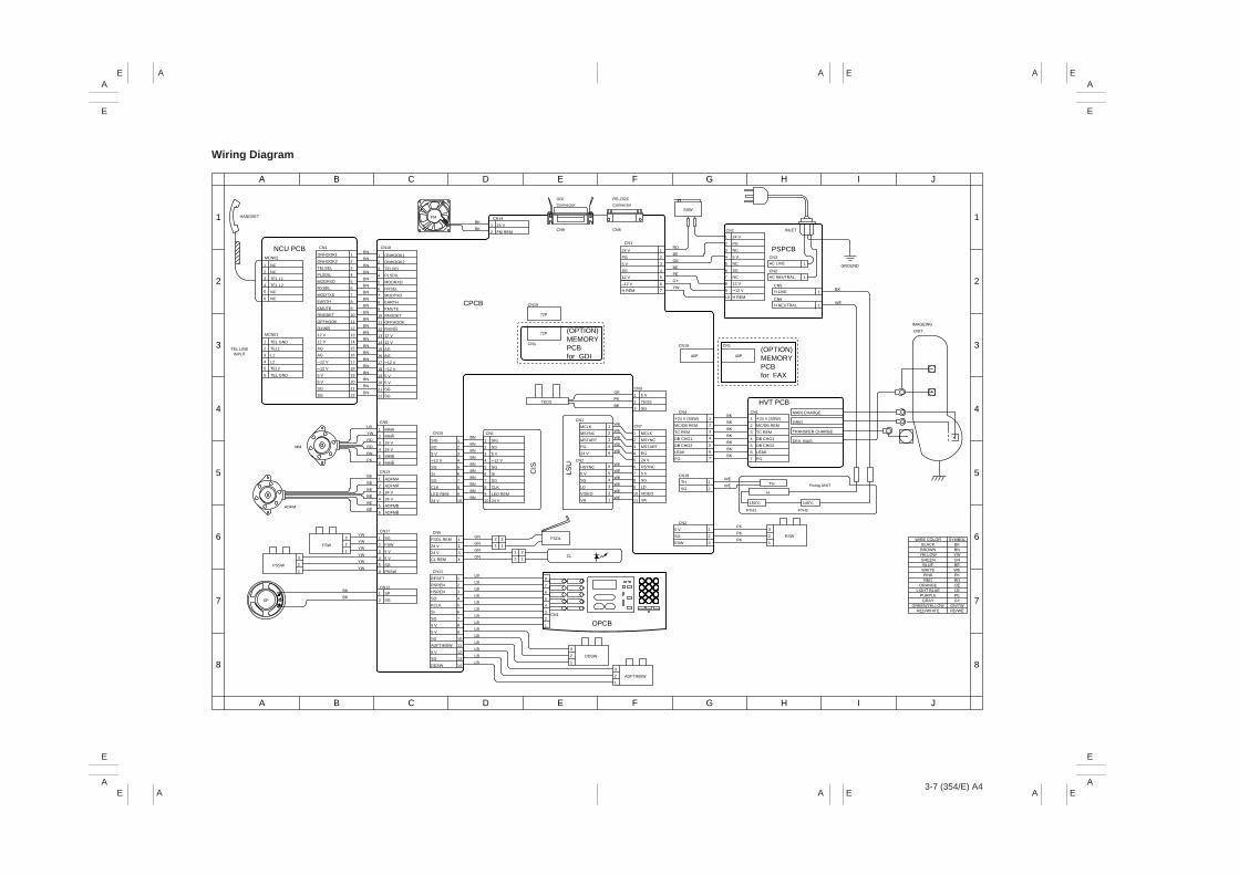
AA A
A
AA A
A
E
E E
E
E
E E
E
EA
EA
3-7 (354/E) A4
A B C D E F G H I J
A B C D E F G H I J
1
2
3
4
5
6
7
8
1
2
3
4
5
6
7
8
Wiring Diagram
ONHOOK1
ONHOOK2
TELSEL
PLSDIL
MODRXD
RXSEL
MODTXD
EARTH
KMUTE
RNGDET
OFFHOOK
RXINN
12 V
12 V
AG
AG
–12 V
–12 V
5 V
5 V
SG
SG
CN2
CN1WE
WE
WE
WE
WE
CN14
GDI
Connector
CN9
RS-232C
Connector
CN8
CN1
INLET
SSW
GROUND
PSPCB
CN12
CN11
CN1 CN10
FM
MCN02
1
2
3
4
5
6
1
2
3
4
5
6
7
8
9
10
11
12
13
14
15
16
17
18
19
20
21
22
1
2
3
4
5
6
7
8
9
10
11
12
13
14
15
16
17
18
19
20
21
22
1
2
3
4
5
6
1
2
3
4
5
6
7
8
9
10
1
2
3
4
5
6
7
8
9
10
SIG
SG
5 V
–12 V
SG
SI
SG
CLK
LED REM
24 V
1
2
3
4
2
1
2
1
1
2
2
1
3
2
1
3
2
1
CN1
FSOL
CL
OPCB
DDSW
ADFTIMSW
FSOL REM
24 V
24 V
CL REM
1
2
3
4
5
6
7
8
9
10
11
12
13
14
RESET
RSREN
HSREN
SO
KCLK
SI
SG
5 V
5 V
SG
ADFTIMSW
5 V
SG
DDSW
SIG
SG
5 V
–12 V
SG
SI
SG
CLK
LED REM
24 V
1
2
3
4
5
6
1
2
3
4
5
6
1
2
SG
FSW
5 V
5 V
SG
PSSW
SP
SG
3
2
1
3
2
1
YW
YW
YW
YW
YW
YW
GN
GN
GN
GN
LB
LB
LB
LB
LB
LB
LB
LB
LB
LB
LB
LB
LB
LB
BE
BE
BE
BE
BE
BE
BN
BN
BN
BN
BN
BN
BN
BN
BN
BN
OE
PK
BE
LB
YW
RD
RD
BN
PK
BK
BK
MMA
MMA
24 V
24 V
MMB
MMB
ADFMA
ADFMA
24 V
24 V
ADFMB
ADFMB
BN
BN
BN
BN
BN
BN
BN
BN
BN
BN
BN
BN
BN
BN
BN
BN
BN
BN
BN
BN
BN
BN
MM
ADFM
FSW
PSSW
SP
NC
NC
TEL L1
TEL L2
NC
NC
1
2
3
4
5
6
TEL GND
TEL1
L1
L2
TEL2
TEL GND
MCN01
TEL LINEINPUT
HANDSET
NCU PCB
CPCB
CIS
LSU
(OPTION)MEMORYPCBfor GDI
CN6
CN13
CN15
CN19
CN1
CN1
72P
72P
CN17 CN5
ONHOOK1
ONHOOK2
TELSEL
PLSDIL
MODRXD
RXSEL
MODTXD
EARTH
KMUTE
RNGDET
OFFHOOK
RXINN
12 V
12 V
AG
AG
–12 V
–12 V
5 V
5 V
SG
SG
BK
BK1
2
24 V
FM REM
8
7
6
5
4
3
2
1
1
2
3
4
5
CN16
40P
CN1
40P
CN7
CN3
CN4 CN1
CN18
CN2
ESW
Fixing UNIT
IMAGEING
UNIT
TEDS
MCLK
MSYNC
MSTART
PG
24 V
6
5
4
3
2
1
HSYNC
5 V
SG
LD
VIDEO
VR
WE
WE
WE
WE
WE
WE
1
2
3
5 V
TEDS
SG
1
2
3
4
5
6
7
8
9
10
11
MCLK
MSYNC
MSTART
PG
24 V
HSYNC
5 V
SG
LD
VIDEO
VR
1
2
3
4
5
6
7
24 V
PG
5 V
SG
12 V
–12 V
H REM
CN1
1
2
3
4
5
6
7
8
9
101
1
24 V
PG
NC
5 V
NC
SG
NC
12 V
–12 V
H REMH LIVE
H NEUTRAL
CN5
CN6
RD
BE
OE
BE
PE
GY
YW BK
WE
(OPTION)MEMORYPCBfor FAX
HVT PCB
1
2
3
4
5
6
7
1
2
3
4
5
6
7
+24 V (SSW)
MC/DB REM
TC REM
DB CHG1
DB CHG2
LEAK
PG
MAIN CHARGE
GRID
TRANSFER CHARGE
DEV. BIAS
TH
H
FTH1 FTH2
150˚C 145˚C
1
2
1
2
3
3
2
1
5 V
SG
ESW
TH
SG
+24 V (SSW)
MC/DB REM
TC REM
DB CHG1
DB CHG2
LEAK
PG
BK
BK
BK
BK
BK
BK
BK
WE
WE
PK
PK
PKBLACKBROWNYELLOWGREENBLUE
WHITEPINKRED
ORANGELIGHT BLUE
PURPLEGRAY
GREEN/YELLOWRED/WHITE
BKBNYWGNBEWEPKRDOELBPEGY
GN/YWRD/WE
WIRE COLOR SYMBOL
1
1
AC LIVE
AC NEUTRAL
CN3
CN2
354
CONTENTS
I THEORY AND CONSTRUCTION SECTION1-1 Specifications
1-1-1 Specifications ................................................................................... 1-1-11-2 Handling Precautions
1-2-1 Consumables ................................................................................... 1-2-11-2-2 Precautions for Operation ................................................................ 1-2-11-2-3 Document ......................................................................................... 1-2-21-2-4 Paper ................................................................................................ 1-2-3
1-3 Mechanical Construction1-3-1 Machine parts names and their functions ......................................... 1-3-11-3-2 Machine cross sections .................................................................... 1-3-81-3-3 Drive system ..................................................................................... 1-3-91-3-4 Mechanical construction ................................................................. 1-3-11
II ELECTRICAL SECTION2-1 Electrical Parts Layout
2-1-1 Electrical parts layout ....................................................................... 2-1-12-2 Detection of Paper Misfeeds
2-2-1 Paper jam detection ......................................................................... 2-2-12-2-2 Paper jam detection conditions ........................................................ 2-2-2
2-3 Operation of the PCB2-3-1 Consists of electric circuit .................................................................. 2-3-12-3-2 Power source PCB ............................................................................ 2-3-22-3-3 Control PCB ...................................................................................... 2-3-32-3-4 NCU PCB (Network control unit PCB) ............................................... 2-3-42-3-5 OPCB (Operation unit PCB) .............................................................. 2-3-52-3-6 Communication Procedures .............................................................. 2-3-6
III SET UP AND ADJUSTMENT SECTION3-1 Installation
3-1-1 Unpacking and installation ............................................................... 3-1-13-1-2 Data setting and registration .......................................................... 3-1-153-1-3 Printing system ............................................................................... 3-1-183-1-4 Scanning system (TWAIN) ............................................................. 3-1-233-1-5 Memory (SIMM) expansion ............................................................. 3-1-26
3-2 Service Mode and Test Mode3-2-1 Outline of service mode and test mode ............................................. 3-2-13-2-2 Service mode .................................................................................... 3-2-23-2-3 Test mode ....................................................................................... 3-2-27
3-3 Assembly and Disassembly3-3-1 Precautions for assembly and disassembly ..................................... 3-3-13-3-2 Outer covers ..................................................................................... 3-3-23-3-3 Paper feed section ............................................................................ 3-3-53-3-4 Document feed and image reading sections (ADF) ........................ 3-3-113-3-5 Optical section ................................................................................. 3-3-193-3-6 Transfer section ............................................................................... 3-3-243-3-7 Fixing section ................................................................................. 3-3-26
3-3-8 PCBs .............................................................................................. 3-3-363-3-9 Adjustment ..................................................................................... 3-3-43
3-4 PCB Initial Setting3-4-1 Replacing the control PCB ............................................................... 3-4-13-4-2 Non-adjustable variable resistors (VR) ............................................. 3-4-2
3-5 Self-diagnostics3-5-1 Abnormality detection ........................................................................ 3-5-13-5-2 Error code tables ............................................................................... 3-5-4
3-6 Troubleshooting3-6-1 Image formation problems ................................................................ 3-6-13-6-2 Paper jams ..................................................................................... 3-6-113-6-3 PCB terminal voltages .................................................................... 3-6-133-6-4 Electrical problems ......................................................................... 3-6-193-6-5 Mechanical problems ...................................................................... 3-6-23
3-7 AppendixesTiming chart No. 1 ...................................................................................... 3-7-1Timing chart No. 2 ...................................................................................... 3-7-2Power source PCB ..................................................................................... 3-7-3HVT (High voltage transformer) PCB ......................................................... 3-7-4Control PCB 1/7 ........................................................................................... 3-7-5Control PCB 2/7 ........................................................................................... 3-7-6Control PCB 3/7 ........................................................................................................................... 3-7-7Control PCB 4/7 ........................................................................................................................... 3-7-8Control PCB 5/7 ........................................................................................................................... 3-7-9Control PCB 6/7 ........................................................................................................................ 3-7-10Control PCB 7/7 ......................................................................................... 3-7-11NCU (Network control unit) PCB .............................................................. 3-7-12Operation unit PCB .................................................................................... 3-7-13Connection Diagram .................................................................................. 3-7-14Wiring Diagram .......................................................................................... 3-7-15
354

354
1-1 Specifications1-1-1 Specifications .................................................................................... 1-1-1
354
1-2 Handling Precautions1-2-1 Consumables .................................................................................... 1-2-1
( 1 ) Paper .......................................................................................... 1-2-1( 2 ) Imaging unit ................................................................................ 1-2-1
1-2-2 Precautions for Operation ................................................................. 1-2-11-2-3 Document .......................................................................................... 1-2-2
( 1 ) Types of document ..................................................................... 1-2-21-2-4 Paper ................................................................................................ 1-2-3
( 1 ) Types of paper ........................................................................... 1-2-3
354
1-3 Mechanical Construction1-3-1 Machine parts names and their functions ......................................... 1-3-1
( 1 ) Main body ................................................................................... 1-3-1( 2 ) Handset (For inch models only) ................................................ 1-3-3( 3 ) Operation panel .......................................................................... 1-3-4
1-3-2 Machine cross sections ..................................................................... 1-3-81-3-3 Drive system ..................................................................................... 1-3-91-3-4 Mechanical construction.................................................................. 1-3-11
( 1 ) Document feed/image reading sections (ADF) ........................ 1-3-11( 2 ) Paper feed section ................................................................... 1-3-13( 3 ) Laser scanning unit .................................................................. 1-3-15( 4 ) Imaging unit .............................................................................. 1-3-18( 5 ) Transfer/charge erasing sections ............................................. 1-3-20( 6 ) Fixing section ........................................................................... 1-3-21

354
2-1 Electrical Parts Layout2-1-1 Electrical parts layout ........................................................................ 2-1-1

354
2-2 Detection of Paper Misfeeds2-2-1 Paper jam detection .......................................................................... 2-2-12-2-2 Paper jam detection conditions ......................................................... 2-2-2
354
2-3 Operation of the PCB2-3-1 Consists of electric circuit .................................................................. 2-3-12-3-2 Power source PCB ............................................................................. 2-3-22-3-3 Control PCB ....................................................................................... 2-3-32-3-4 NCU PCB (Network control unit PCB) ............................................... 2-3-42-3-5 OPCB (Operation unit PCB) .............................................................. 2-3-52-3-6 Communication Procedures ............................................................... 2-3-6
( 1 ) Outline ........................................................................................ 2-3-6( 2 ) Communication Procedures ....................................................... 2-3-7

354
3-1 Installation3-1-1 Unpacking and installation ................................................................ 3-1-1
( 1 ) Installation environment ............................................................ 3-1-1( 2 ) Installation procedure ................................................................ 3-1-2
3-1-2 Data setting and registration ........................................................... 3-1-15( 1 ) Setting ..................................................................................... 3-1-15( 2 ) Registration ............................................................................. 3-1-17
3-1-3 Printing system ............................................................................... 3-1-18( 1 ) Recommended computer environment .................................... 3-1-18( 2 ) Connecting the machine to your computer ............................... 3-1-19( 3 ) Installing the printer driver and connecting to the printer
in Windows 3.1 ........................................................................ 3-1-20(3-1) Installing the printer driver ............................................... 3-1-20(3-2) Connecting to the printer ................................................. 3-1-20
( 4 ) Installing the printer driver, connecting to the printerand making a test print in Windows 95 ..................................... 3-1-21(4-1) Installing the printer driver ............................................... 3-1-21(4-2) Connecting to the machine and making a test print ........ 3-1-22
3-1-4 Scanning system (TWAIN) .............................................................. 3-1-23( 1 ) Recommended computer environment .................................... 3-1-23( 2 ) Connecting the machine to your computer ............................... 3-1-24( 3 ) Installing the TWAIN system .................................................... 3-1-25
(3-1) Windows 3.1 .................................................................... 3-1-25(3-2) Windows 95 ..................................................................... 3-1-25
3-1-5 Memory (SIMM) expansion .............................................................. 3-1-26
354
3-2 Service Mode and Test Mode3-2-1 Outline of service mode and test mode ............................................. 3-2-13-2-2 Service mode ..................................................................................... 3-2-2
( 1 ) Memory switch settings .............................................................. 3-2-3( 2 ) Memory switch default setting .................................................... 3-2-4( 3 ) Memory switch description ......................................................... 3-2-6
3-2-3 Test mode ........................................................................................ 3-2-27( 1 ) Reading test mode ................................................................... 3-2-28( 2 ) Modem test mode ..................................................................... 3-2-29( 3 ) Print test mode ......................................................................... 3-2-31( 4 ) Aging test mode ....................................................................... 3-2-33( 5 ) ADF adjustment mode .............................................................. 3-2-35
354
3-3 Assembly and Disassembly3-3-1 Precautions for assembly and disassembly ...................................... 3-3-13-3-2 Outer covers ..................................................................................... 3-3-2
( 1 ) Detaching and refitting the rear cover and right cover ............... 3-3-2( 2 ) Detaching and refitting the left cover and left front cover ........... 3-3-3( 3 ) Detaching and refitting the upper cover ..................................... 3-3-4( 4 ) Detaching and refitting the base lid ............................................ 3-3-4
3-3-3 Paper feed section ............................................................................. 3-3-5( 1 ) Detaching and refitting the paper feed pulley ............................. 3-3-5( 2 ) Detaching and refitting the paper feed pad ................................ 3-3-7( 3 ) Detaching and refitting the lower feed roller ............................... 3-3-8( 4 ) Detaching and refitting the upper feed roller ............................ 3-3-10
3-3-4 Document feed and image reading sections (ADF) ......................... 3-3-11( 1 ) Detaching and refitting the ADF guide ..................................... 3-3-11( 2 ) Detaching and refitting the ADF housing .................................. 3-3-12( 3 ) Detaching and refitting the contact image sensor (CIS) ........... 3-3-13( 4 ) Detaching and refitting the ADF pad ........................................ 3-3-15( 5 ) Detaching and refitting the ADF paper feed roller
and ADF conveying roller ......................................................... 3-3-16( 6 ) Detaching and refitting the ADF eject roller .............................. 3-3-18
3-3-5 Optical section.................................................................................. 3-3-19( 1 ) Detaching and refitting the laser scanning unit ........................ 3-3-19
3-3-6 Transfer section ............................................................................... 3-3-24( 1 ) Detaching and refitting the transfer roller ................................ 3-3-24
3-3-7 Fixing section .................................................................................. 3-3-26( 1 ) Detaching and refitting the fixing thermistor ............................. 3-3-26( 2 ) Detaching and refitting the fixing heater ................................... 3-3-29( 3 ) Detaching and refitting the heat roller ...................................... 3-3-31( 4 ) Detaching and refitting the press roller ..................................... 3-3-32( 5 ) Detaching and refitting the separation claw ............................. 3-3-33( 6 ) Detaching and refitting the fixing thermostat 1 and 2 ............... 3-3-34( 7 ) Detaching and refitting the eject roller ...................................... 3-3-35
3-3-8 PCBs ............................................................................................... 3-3-36( 1 ) Detaching and refitting the control PCB (CPCB) ...................... 3-3-36( 2 ) Detaching and refitting the NCU PCB ...................................... 3-3-37( 3 ) Detaching and refitting the high voltage transformer PCB ....... 3-3-38( 4 ) Detaching and refitting the power source PCB ........................ 3-3-40( 5 ) Detaching and refitting the operation unit ................................. 3-3-42
3-3-9 Adjustment ...................................................................................... 3-3-43( 1 ) Adjusting the document reading density threshold ................... 3-3-43( 2 ) Adjusting the paper leading edge registration timing ............... 3-3-44( 3 ) Adjusting the center registration ............................................... 3-3-46( 4 ) Adjusting the document leading edge registration timing ......... 3-3-48( 5 ) Adjusting the document trailing edge registration timing .......... 3-3-50( 6 ) Adjusting the document reading start position
(main scanning direction) ......................................................... 3-3-52

354
3-4 PCB Initial Setting3-4-1 Replacing the control PCB ................................................................ 3-4-13-4-2 Non-adjustable variable resistors (VR) ............................................. 3-4-2

354
3-5 Self-diagnostics3-5-1 Abnormality detection ........................................................................ 3-5-13-5-2 Error code tables ................................................................................ 3-5-4
354
3-6 Troubleshooting3-6-1 Image formation problems ................................................................ 3-6-1
( 1 ) No printing (entirely white). ........................................................ 3-6-3( 2 ) No printing (entirely black). ........................................................ 3-6-3( 3 ) Printing is too light. .................................................................... 3-6-4( 4 ) Background is visible. ................................................................ 3-6-4( 5 ) A white line appears longitudinally. ........................................... 3-6-5( 6 ) A black line appears longitudinally. ........................................... 3-6-5( 7 ) A black line appears laterally. .................................................... 3-6-6( 8 ) One side of the printing is darker than the other. ...................... 3-6-6( 9 ) Black dots appear on the printing. ............................................. 3-6-7(10) Printing is blurred. ...................................................................... 3-6-7(11) The leading edge of the printing is consistently misaligned
with the original. ........................................................................ 3-6-8(12) Paper creases. .......................................................................... 3-6-8(13) Offset occurs. ............................................................................ 3-6-9(14) Printing is party missing. ............................................................ 3-6-9(15) Fixing is poor. .......................................................................... 3-6-10
3-6-2 Paper jams ...................................................................................... 3-6-113-6-3 PCB terminal voltages .................................................................... 3-6-13
( 1 ) Power source PCB .................................................................. 3-6-13( 2 ) Control PCB ............................................................................ 3-6-14( 3 ) Operation unit PCB ................................................................. 3-6-17( 3 ) Network control unit PCB ........................................................ 3-6-18
3-6-4 Electrical problems .......................................................................... 3-6-19( 1 ) The machine does not operate when the power plug is
connected to a wall outlet. ....................................................... 3-6-19( 2 ) Error indicator lamp lights. ....................................................... 3-6-19( 3 ) The main motor does not rotate. ............................................. 3-6-20( 4 ) The paper feed solenoid does not operate. ............................. 3-6-20( 5 ) The cooling fan motor does not rotate. .................................... 3-6-20( 6 ) The ADF motor does not rotate. .............................................. 3-6-20( 7 ) The fixing heater does not turn on.
(Fixing thermostat 1, 2 operates.) ........................................... 3-6-21( 8 ) The fixing heater does not turn off. .......................................... 3-6-21( 9 ) The cleaning lamp does not light. ............................................ 3-6-21(10) Main charger does not turn on.
(The paper is printed in all black.) ........................................... 3-6-21(11) No developing bias voltage is output.
(Print density is extremely light.) ............................................. 3-6-22(12) Transfer charging is not performed.
(The paper is not printed at all.) .............................................. 3-6-22(13) No sound coming from the speaker ........................................ 3-6-22
3-6-5 Mechanical problems ....................................................................... 3-6-23( 1 ) No document feed. ................................................................... 3-6-23( 2 ) Skewed document feed. ........................................................... 3-6-23( 3 ) Multiple sheets of document are fed at one time. ..................... 3-6-23( 4 ) Document jam .......................................................................... 3-6-23

( 5 ) No paper feed. .......................................................................... 3-6-23( 6 ) Skewed paper feed. ................................................................. 3-6-24( 7 ) Multiple sheets of paper are fed at one time. ........................... 3-6-24( 8 ) Paper jam. ................................................................................ 3-6-24( 9 ) Toner drops on the inner machine. .......................................... 3-6-24(10) Abnormal noise is heard. .......................................................... 3-6-24
354

354
3-7 AppendixesTiming chart No. 1 ......................................................................................... 3-7-1Timing chart No. 2 ......................................................................................... 3-7-2Power source PCB ........................................................................................ 3-7-3HVT (High voltage transformer) PCB ............................................................ 3-7-4Control PCB 1/7 ............................................................................................. 3-7-5Control PCB 2/7 ............................................................................................. 3-7-6Control PCB 3/7 .............................................................................................................................. 3-7-7Control PCB 4/7 .............................................................................................................................. 3-7-8Control PCB 5/7 .............................................................................................................................. 3-7-9Control PCB 6/7 ........................................................................................................................... 3-7-10Control PCB 7/7 ........................................................................................... 3-7-11NCU (Network control unit) PCB ................................................................. 3-7-12Operation unit PCB ...................................................................................... 3-7-13Connection Diagram .................................................................................... 3-7-14Wiring Diagram ............................................................................................ 3-7-15
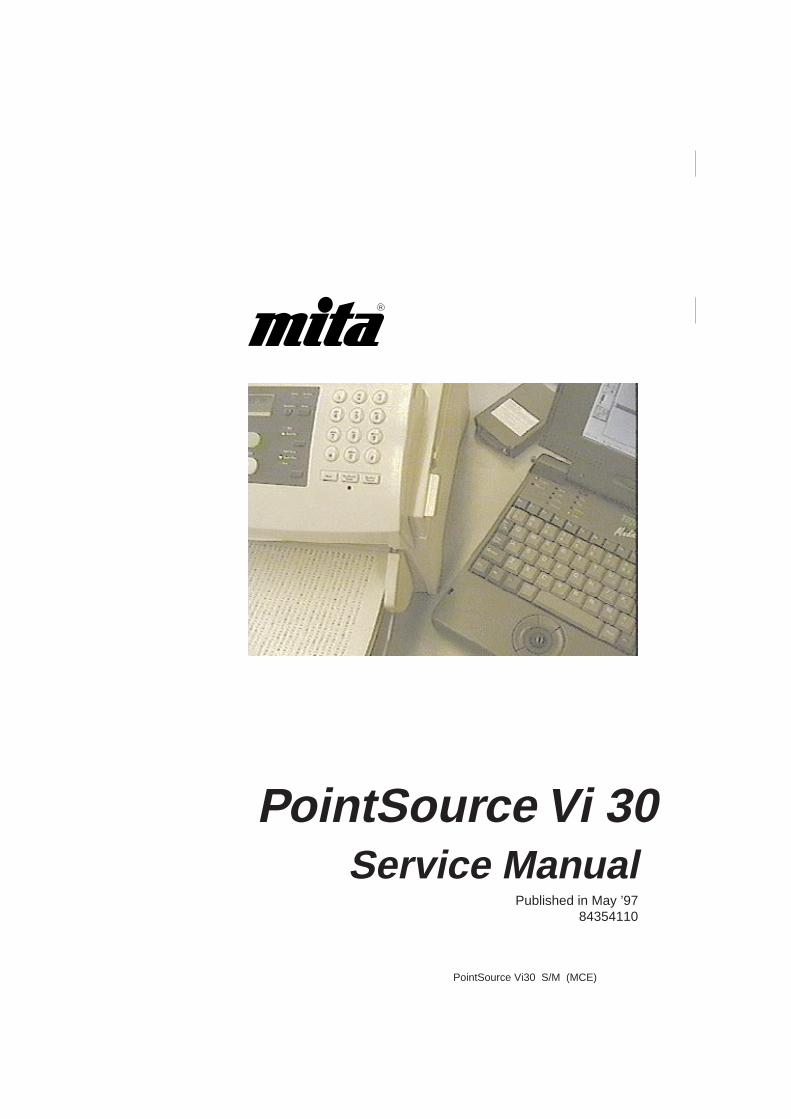
PointSource Vi30 S/M (MCE)
Service ManualPublished in May ’97
84354110
R
PointSource Vi 30
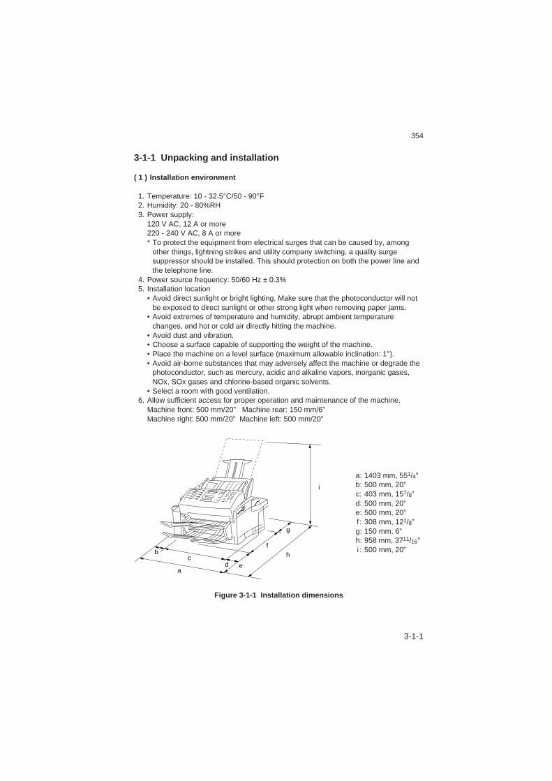
3-1-1
354
3-1-1 Unpacking and installation
( 1 ) Installation environment
1. Temperature: 10 - 32.5°C/50 - 90°F 2. Humidity: 20 - 80%RH 3. Power supply:
120 V AC, 12 A or more220 - 240 V AC, 8 A or more* To protect the equipment from electrical surges that can be caused by, among
other things, lightning strikes and utility company switching, a quality surgesuppressor should be installed. This should protection on both the power line andthe telephone line.
4. Power source frequency: 50/60 Hz ± 0.3% 5. Installation location
• Avoid direct sunlight or bright lighting. Make sure that the photoconductor will notbe exposed to direct sunlight or other strong light when removing paper jams.
• Avoid extremes of temperature and humidity, abrupt ambient temperaturechanges, and hot or cold air directly hitting the machine.
• Avoid dust and vibration.• Choose a surface capable of supporting the weight of the machine.• Place the machine on a level surface (maximum allowable inclination: 1°).• Avoid air-borne substances that may adversely affect the machine or degrade the
photoconductor, such as mercury, acidic and alkaline vapors, inorganic gases,NOx, SOx gases and chlorine-based organic solvents.
• Select a room with good ventilation. 6. Allow sufficient access for proper operation and maintenance of the machine.
Machine front: 500 mm/20” Machine rear: 150 mm/6”Machine right: 500 mm/20” Machine left: 500 mm/20”
bc
da
e
f
g
h
i
Figure 3-1-1 Installation dimensions
a: 1403 mm, 551/4”b: 500 mm, 20”c: 403 mm, 157/8”d: 500 mm, 20”e: 500 mm, 20”f : 308 mm, 121/8”g: 150 mm, 6”h: 958 mm, 3711/16”i : 500 mm, 20”
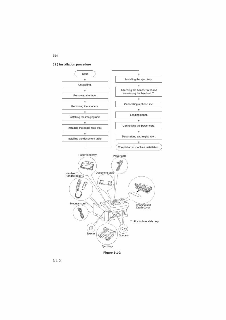
3-1-2
354
( 2 ) Installation procedure
Data setting and registration.
Completion of machine installation.
Removing the tape.
Removing the spacers.
Installing the eject tray.
Connecting a phone line.
Attaching the handset rest and connecting the handset. *1
Start
Unpacking.
Connecting the power cord.
Loading paper.Installing the imaging unit.
Installing the paper feed tray.
Installing the document table.
Paper feed tray
Document table
Power cord
Imaging unitDrum cover
*1: For inch models only
SpacersSpacer
Modular cord
Handset *1Handset rest *1
Eject tray
Figure 3-1-2
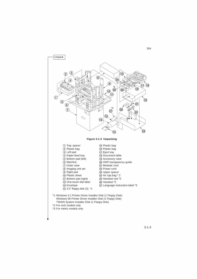
3-1-3
354
15
6
7
2
4
3
8
9
0!
fi
‡
@#
$
fl^&
*
›
(
¤
⁄
)
‹
%
*2
*2
*3
*2
Figure 3-1-3 Unpacking
*1: Windows 3.1 Printer Driver Installer Disk (1 Floppy Disk)Windows 95 Printer Driver Installer Disk (1 Floppy Disk)TWAIN System Installer Disk (1 Floppy Disk)
*2: For inch models only*3: For metric models only
Unpack.
% Plastic bag^ Plastic bag& Eject tray* Document table( Accessory case) OHP transparency guide⁄ Modular cord¤ Power cord‹ Upper spacer› Air cap bag * 2fi Handset rest *2fl Handset *2‡ Language instruction label *3
1 Tray spacer2 Plastic bag3 Left pad4 Paper feed tray5 Bottom pad (left)6 Machine7 Outer case8 Imaging unit set9 Right pad0 Plastic sheet! Bottom pad (right)@ One-touch dial label# Envelope$ 3.5" floppy disk (3) *1
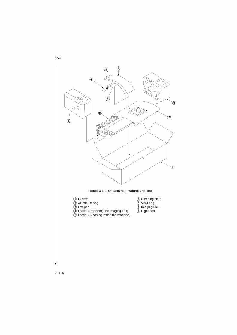
3-1-4
354
9
6
5 4
7
8
3
2
1
Figure 3-1-4 Unpacking (Imaging unit set)
6 Cleaning cloth7 Vinyl bag8 Imaging unit9 Right pad
1 IU case2 Aluminum bag3 Left pad4 Leaflet (Replacing the imaging unit)5 Leaflet (Cleaning inside the machine)
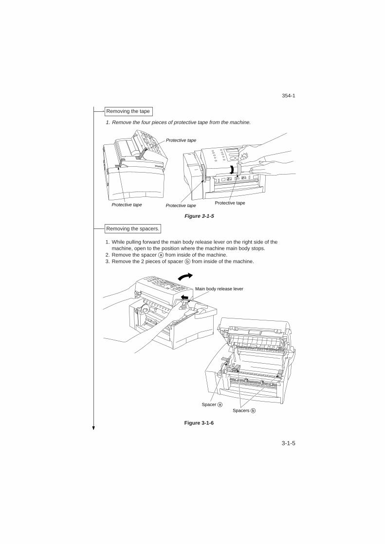
3-1-5
354
.
1. Remove the four pieces of protective tape from the machine.
Protective tapeProtective tape
Protective tape
Protective tape
Figure 3-1-5
1. While pulling forward the main body release lever on the right side of themachine, open to the position where the machine main body stops.
2. Remove the spacer a from inside of the machine. 3. Remove the 2 pieces of spacer b from inside of the machine.
Main body release lever
Spacer aSpacers b
Figure 3-1-6
Removing the tape
Removing the spacers.
354-1
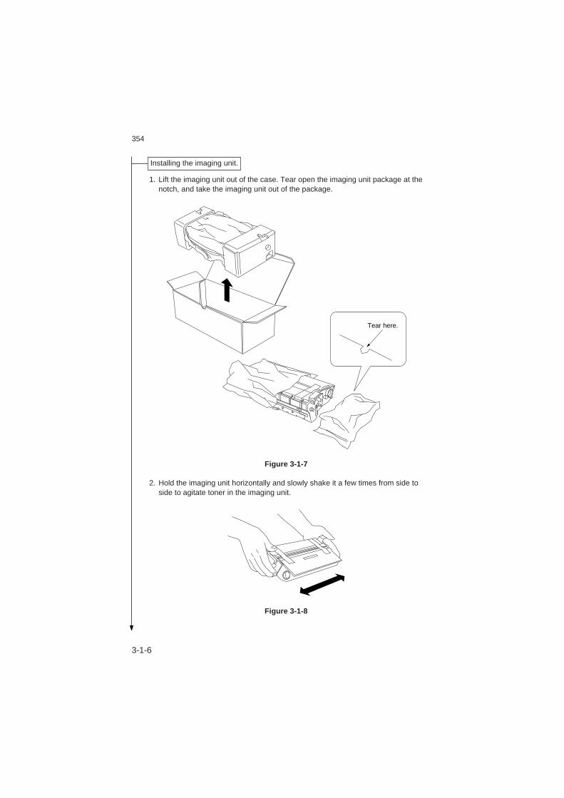
3-1-6
354
1. Lift the imaging unit out of the case. Tear open the imaging unit package at thenotch, and take the imaging unit out of the package.
Tear here.
Figure 3-1-7
2. Hold the imaging unit horizontally and slowly shake it a few times from side toside to agitate toner in the imaging unit.
Figure 3-1-8
Installing the imaging unit.

3-1-7
354
3. Hold the imaging unit left and right handles, check that the imaging unit isaligned forward-rear, then install the imaging unit on the machine main body asshown in the figure.
4. Remove the protective tapes on both sides of the imaging unit, and thenremove the drum cover from the unit.
Handles
Protective tapes
Drum cover
Figure 3-1-9
5. Gently close the machine. * If the machine does not close properly, the imaging unit may not be set
properly. Reinstall the imaging unit correctly.
Figure 3-1-10
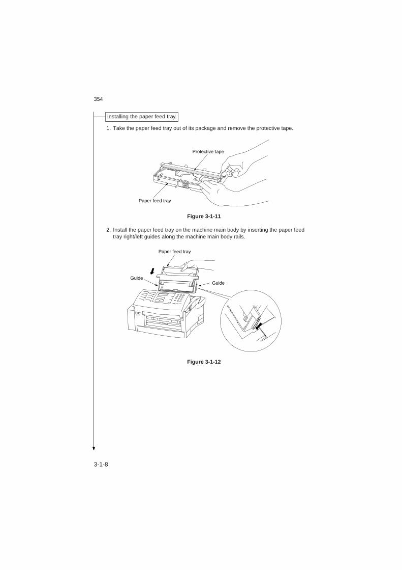
3-1-8
354
1. Take the paper feed tray out of its package and remove the protective tape.
Paper feed tray
Protective tape
Figure 3-1-11
2. Install the paper feed tray on the machine main body by inserting the paper feedtray right/left guides along the machine main body rails.
Paper feed tray
GuideGuide
Figure 3-1-12
Installing the paper feed tray.
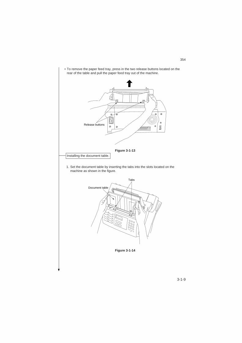
3-1-9
354
• To remove the paper feed tray, press in the two release buttons located on therear of the table and pull the paper feed tray out of the machine.
Release buttons
Figure 3-1-13
1. Set the document table by inserting the tabs into the slots located on themachine as shown in the figure.
Tabs
Document table
Figure 3-1-14
Installing the document table.
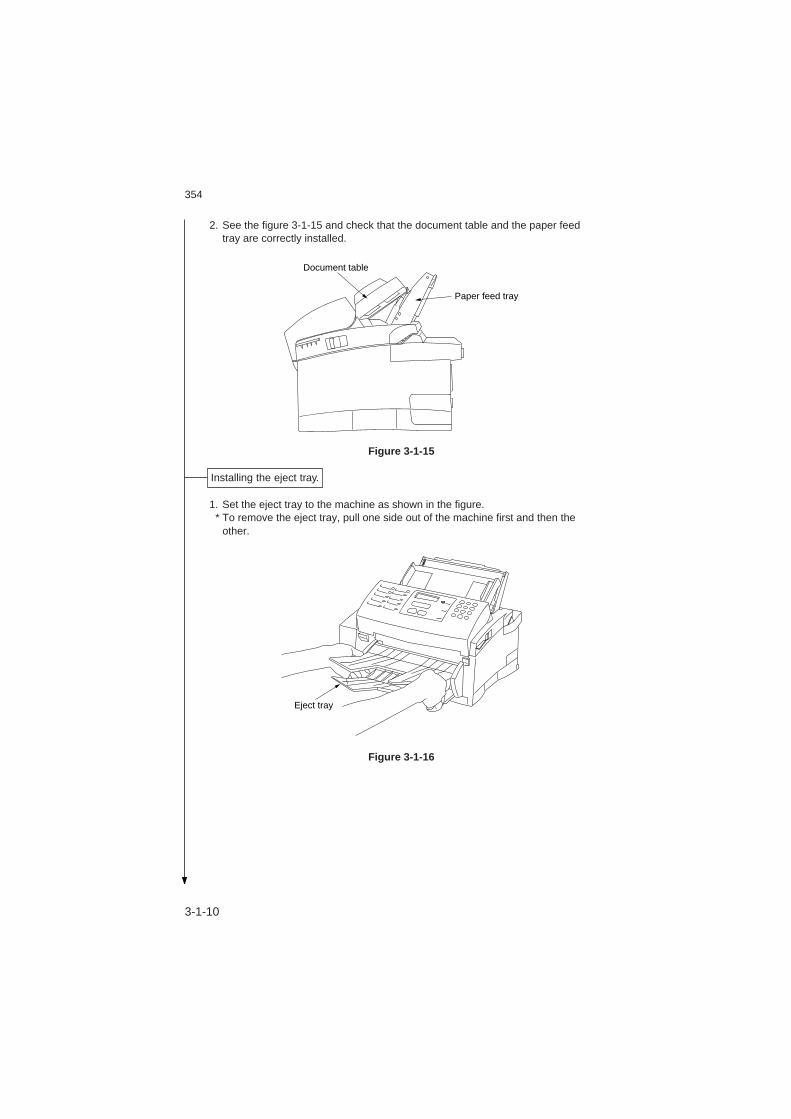
3-1-10
354
2. See the figure 3-1-15 and check that the document table and the paper feedtray are correctly installed.
Paper feed tray
Document table
Figure 3-1-15
1. Set the eject tray to the machine as shown in the figure. * To remove the eject tray, pull one side out of the machine first and then the
other.
Eject tray
Figure 3-1-16
Installing the eject tray.

3-1-11
354
1. Remove the tape from the rear of the handset rest. 2. Insert the hooks of the handset rest into the holes located on the machine to
install it as shown in the figure.
Handset rest
Figure 3-1-17
3. Plug the handset cord into the telephone jack on the machine. 4. Set the handset onto the handset rest.
Telephone jack
Figure 3-1-18
Attaching the handset rest and connecting the handset. (For inch models only)

3-1-12
354
1. Plug one end of the modular cord into the line jack on the machine and theother end into the phone jack in the room.
Line jack
Figure 3-1-19
1. Extend the paper feed tray extension. 2. Open the paper feed tray cover.
Paper feed tray extension
Paper feed tray cover
Figure 3-1-20
Connecting a phone line.
Loading paper.
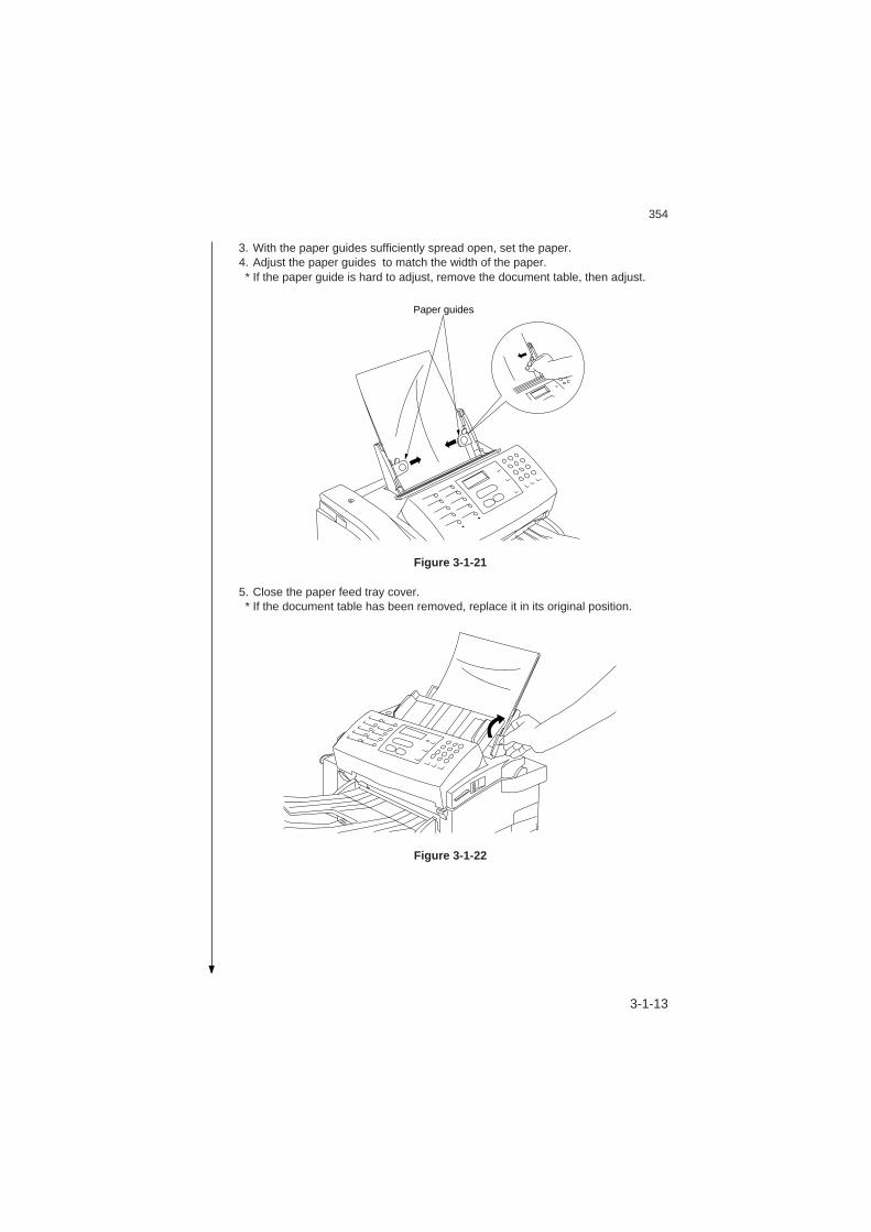
3-1-13
354
3. With the paper guides sufficiently spread open, set the paper. 4. Adjust the paper guides to match the width of the paper. * If the paper guide is hard to adjust, remove the document table, then adjust.
Paper guides
Figure 3-1-21
5. Close the paper feed tray cover. * If the document table has been removed, replace it in its original position.
Figure 3-1-22
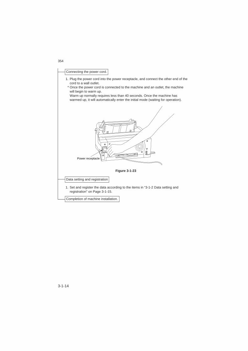
3-1-14
354
1. Plug the power cord into the power receptacle, and connect the other end of thecord to a wall outlet.
* Once the power cord is connected to the machine and an outlet, the machinewill begin to warm up.Warm up normally requires less than 40 seconds. Once the machine haswarmed up, it will automatically enter the initial mode (waiting for operation).
Power receptacle
Figure 3-1-23
1. Set and register the data according to the items in “3-1-2 Data setting andregistration” on Page 3-1-15.
Data setting and registration
Completion of machine installation.
Connecting the power cord.
3-1-15
354
3-1-2 Data setting and registration
When the machine is installed, the following items are set or registered.
( 1 ) Setting
• Line type settingSelect the setting (dial line or push-tone line) that matches the telephone line used.
• Paper size settingSet the size of paper used for fax reception (A4, letter (81/2" x 11"), or legal (81/2" x14")).
• Automatic reception mode settingSelect the desired automatic reception mode (fax-only dedicated reception mode orfax/telephone automatic switching reception mode).
• Memory reception settingSets whether or not to carry out normal memory reception.
• Memory transfer settingSets whether or not to use the memory transfer function.
• Activity report output condition settingSets the condition for outputting activity report (output every 40 communications,outputs the contents of 24 hours of communications at the set time).
• Transmission report output settingSets the output condition for transmission report (no output or always outputimmediately at end of transmission).
• Speaker ON/OFF settingFor manual reception, sets whether or not the calling sounds from the other party aremonitored on the speaker without picking up the external telephone set receiver whenthe On-Hook/Clear key is pressed.
• Preheat mode settingSets the condition under which this machine moves to the preheat state (after fiveminutes without operation or at the set time).
• PSTN/PBX settingSelect the setting for the exchange system (PSTN or PBX) to which this machine isconnected.
• ECM transmission settingSets whether or not ECM transmission is used.
• User memory settingSets the various memory switches that can be set by the user.The contents of the setting are as follows.
* Number of rings setting (Memory Switch No. 04)For automatic fax reception, sets the number of rings (1-11) from the arrival of thecall to the start of reception.
* Speaker volume setting (Memory Switch No. 06)Sets the speaker volume (3 levels).

3-1-16
354
* Reception time printing setting (Memory Switch No. 16)Sets whether or not the reception year/month/day and time are recorded when adocument is received.
* Error (Alarm) sound setting (Memory Switch No. 54)Sets whether or not there is a beep when an error occurs.
* Speaker sound setting (Memory Switch No. 56)Sets whether or not there is sound from the speaker.
* Other party recording setting (Memory Switch No. 66)Sets whether or not the other party information (fax number, name, etc.) is recordedon reports.
* Memory input report setting (Memory Switch No. 73)Sets whether or not a memory input report is output when a document is scannedduring transmission.
* Superfine setting (Memory Switch No. 89)Sets whether or not copying and reception in superfine mode is enabled.
* Operator-Call bell setting (Memory Switch No. 93)For fax/telephone automatic switching mode, sets the bell volume (3 levels) whenthe incoming call is a telephone (not a fax).
* Transmission mode setting (Memory Switch No. 94)Sets the transmission mode (ADF transmission or memory transmission).
* Transmission results report image attachment setting (Memory Switch No. 96)Sets whether or not the image of the first page transmitted is attached totransmission results reports.
* Printing system time-out setting (Memory Switch No. 97)Sets whether or not this machine is returned to fax standby status when no imagedata is sent from the computer for a certain time during printing with the printingsystem.
* Number of rings setting (TAD/message telephone reception) (Memory Switch No.98)Sets the number of rings (1-11) for message telephone reception.

3-1-17
354
( 2 ) Registration
• Date and time registrationRegisters the current date and time.
• Own station data registrationRegisters your telephone number and station name.
• One-touch speed dialingRegisters the other party’s facsimile number (telephone number) and name for tenone-touch speed dialing keys.
• Abbreviation dialingRegisters the other party’s facsimile number (telephone number) and name for desiredabbreviated number (numeric character 01 to 50).
• Group dialingRegisters multiple other parties’ facsimile numbers (telephone numbers) and namesfor ten one-touch speed dialing keys and registers them for group dialing.
• Batch dialingRegisters the transmission time and multiple other parties’ facsimile numbers(telephone numbers) and names for one of ten one-touch speed dialing keys andregisters them for batch dialing.
• Remote switching dialing numberChanges the remote switching number (set to 55 at the factory) for fax reception withan external telephone.
• PasswordFor memory reception, registers the password (4 digits) for outputting the document.

3-1-18
354
3-1-3 Printing system
This machine can be used as a printer for a computer running Windows 3.1 or Windows95. It is also possible to print under the DOS mode of both systems using PCLemulation.* In this section, there is only list of method to check of computer connection, printer
driver installation, and computer output port.For more detailed information, see the instruction handbook of this machine orinstruction manual of each application software.
( 1 ) Recommended computer environment
The computer configuration recommended for running the printing system underWindows 3.1 or Windows 95 are as follows.
[ Windows 3.1]• IBM PC-AT or compatible• Minimum 20MHz 486SX CPU• Minimum 8MB installed RAM• 5MB free hard disk space• 1 parallel port• 3.5" floppy disk drive• 1 parallel cable (IEEE 1284 specifications)
[ Windows 95 ]• IBM PC-AT or compatible• Minimum 33MHz 486DX CPU• Minimum 8MB installed RAM• 5MB free hard disk space• 1 parallel port• 3.5" floppy disk drive• 1 parallel cable (IEEE 1284 specifications)
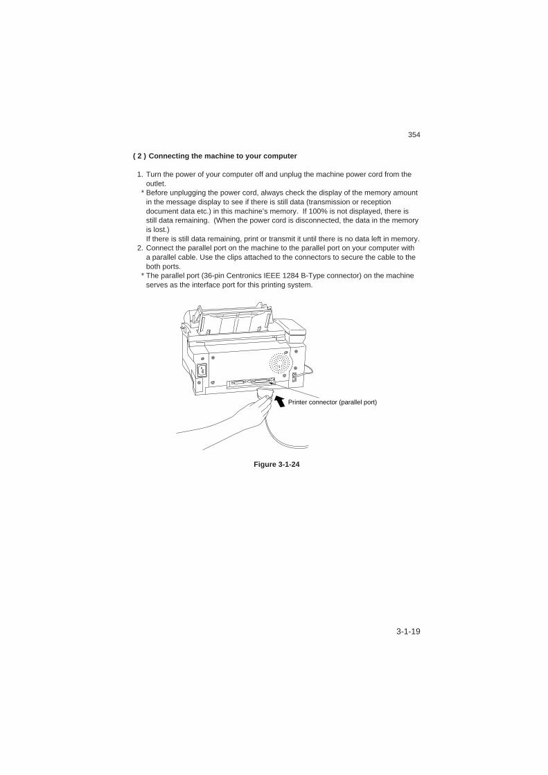
3-1-19
354
( 2 ) Connecting the machine to your computer
1. Turn the power of your computer off and unplug the machine power cord from theoutlet.
* Before unplugging the power cord, always check the display of the memory amountin the message display to see if there is still data (transmission or receptiondocument data etc.) in this machine’s memory. If 100% is not displayed, there isstill data remaining. (When the power cord is disconnected, the data in the memoryis lost.)If there is still data remaining, print or transmit it until there is no data left in memory.
2. Connect the parallel port on the machine to the parallel port on your computer witha parallel cable. Use the clips attached to the connectors to secure the cable to theboth ports.
* The parallel port (36-pin Centronics IEEE 1284 B-Type connector) on the machineserves as the interface port for this printing system.
Printer connector (parallel port)
Figure 3-1-24
3-1-20
354
( 3 ) Installing the printer driver and connecting to the printer in Windows 3.1
(3-1) Installing the printer driver* The following procedure will assume Floppy Drive A is available.
1. Start up Windows 3.1. Quit all other applications that may be open and start upProgram Manager.
2. Insert the Windows 3.1 Printer Driver Installer Disk into Drive A. 3. Use the mouse to point to File in the Menu Bar and click on Run… in the drop-
down menu which is displayed. 4. Type a:\install in the Command Line dialog box and then click on OK. 5. The installation window will appear. To continue the installation, click on Continue . 6. A window will appear to confirm which floppy drive the Installer Disk is in. Make sure
that A:\ is displayed and click on OK. 7. Another window to reconfirm the floppy drive will appear. Click on OK. Installation of
the printer driver will begin. 8. Once installation is complete, Restart Windows now? will appear. To finalize the
installation procedure, restart Windows 3.1 by clicking on Restart Windows . 9. Once Windows 3.1 is running again, an icon with the name of this printer will
appear.The facsimile may now be used as a printer.
(3-2) Connecting to the printerThe factory default setting for the printer output port on most computers is LPT1.Usually there is no need to change this setting, but, in order to confirm the presentsetting in your computer, as well as to change it if it does become necessary, carry outthe following procedure.
1. Double-click on the Control Panel icon in the Main group in Program Manager. 2. Double-click on the Printers applet in the Control Panel window. The Printers
dialog box will appear. 3. Make sure that the printer is shown as being connected to the LPT1 port. If it is not,
click on Connect…. The Connect dialog box will appear. * Select the LPT1 port from the Ports list and click on OK to return to the Printers
dialog box. 4. If this printer is not selected as the default setting in the Printers dialog box, click on
Set as Default Printer . * This printer driver will ignore any settings in the Use Print Manager window.
3-1-21
354
( 4 ) Installing the printer driver, connecting to the printer and making a test printin Windows 95
(4-1) Installing the printer driver* The following procedure will assume Floppy Drive A is available.
1. Start up Windows 95. Quit all other applications that may be open. 2. Insert the Windows 95 Printer Driver Installer Disk into Drive A. 3. Click on Start in the Task Bar. 4. Use the mouse to point to Settings and click on Printers in submenu which is
displayed. 5. The Printers folder will open. Double-click on the Add printer icon. 6. The Printer wizard window will open. Click on Next > . 7. A window which will allow you to select the type of printer connection will appear.
Make sure that Local printer is selected and click on Next > . 8. A list of makers and printer names will be displayed. Do not select a printer from this
list, but instead click on Have Disk . 9. The Install From Disk window will appear. Make sure that Floppy Drive A is
displayed and click on OK. The name of this printer will be displayed. Click on Next>.
10. The Available ports list will appear. Make sure that the port to which the printer isconnected (usually LPT1) is highlighted and click on Next > .
11. The Printer wizard window will display the default name for the printer.If desired, you may change the displayed printer name. Even if the name ischanged, operation will not be affected.
12. Click on Yes to select this printer as the default printer. If you do not want thisprinter to be the default printer, click on No.
13. Click on Finish .Installation of the printer driver will begin. Once the icon with the name of this printerappears in the Printers folder, installation is complete.
The facsimile may now be used as a printer.
3-1-22
354
(4-2) Connecting to the machine and making a test printThe factory default setting for the printer output port on most computers is LPT1.Usually there is no need to change this setting, but, in order to confirm the presentsetting in your computer, as well as to change it if it does become necessary, carry outthe following procedure.
1. Click on Start in the Task Bar. Use the mouse to point to Settings and click onPrinters in the submenu which is displayed.
2. The Printers folder will open. Use the right mouse button to click on the icon for thisprinter.
3. Make sure that there is a check mark to the left of Set As Default in the drop-downmenu which is displayed.If there is no check mark next to it, click on Set As Default and use the right mousebutton to click on the icon for this printer once again.
4. Click on Properties in the menu which is displayed and then click on the Detailstab in the window which appears.
5. Make sure that the LPT1 port is shown in the text box under Ports . If it is not, usethe mouse to click on the drop-down arrow in the right of the text box and check theavailable ports from the drop-down list which is displayed.
6. Click on the General tab and then on Print . A test page will be printed out. * If a Status Window dialog box appears when Properties is selected and a test
page printed out, check to see that….• The power cord is connected correctly to the printer.• An appropriate parallel cable is attached securely to both the printer and computer
ports. 7. Once the test page is printed out successfully and operation is normal, click on OK
to close the Properties dialog box.

3-1-23
354
3-1-4 Scanning system (TWAIN)
* In this section, there is only list of method to check of computer connection, scannerdriver (TWAIN) installation, and computer output port.For more detailed information, see the instruction handbook of this machine orinstruction manual of each application software.
( 1 ) Recommended computer environment
The computer configuration recommended for running the scanning system underWindows 3.1 and Windows 95 are as follows.
• IBM PC-AT or compatible• Minimum 33MHz 486SX CPU• Windows 3.1: Minimum 8MB installed RAM, Windows 95: Minimum 16MB installed
RAM• 32MB free hard disk space• 1 serial port• 3.5" floppy disk drive• 1 RS-232C cable
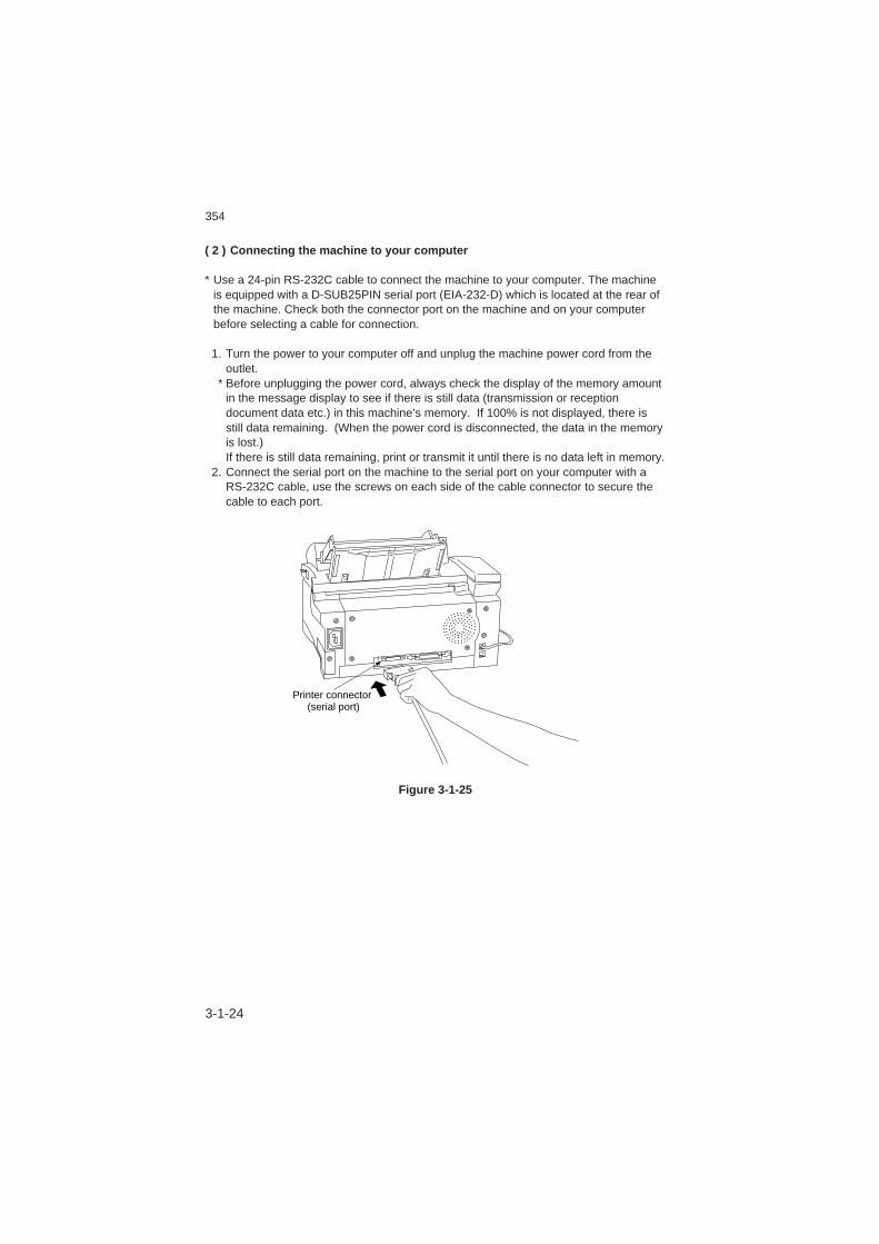
3-1-24
354
( 2 ) Connecting the machine to your computer
* Use a 24-pin RS-232C cable to connect the machine to your computer. The machineis equipped with a D-SUB25PIN serial port (EIA-232-D) which is located at the rear ofthe machine. Check both the connector port on the machine and on your computerbefore selecting a cable for connection.
1. Turn the power to your computer off and unplug the machine power cord from theoutlet.
* Before unplugging the power cord, always check the display of the memory amountin the message display to see if there is still data (transmission or receptiondocument data etc.) in this machine’s memory. If 100% is not displayed, there isstill data remaining. (When the power cord is disconnected, the data in the memoryis lost.)If there is still data remaining, print or transmit it until there is no data left in memory.
2. Connect the serial port on the machine to the serial port on your computer with aRS-232C cable, use the screws on each side of the cable connector to secure thecable to each port.
Printer connector (serial port)
Figure 3-1-25
3-1-25
354
( 3 ) Installing the TWAIN system
(3-1) Windows 3.1* The following procedure will assume Floppy Drive A is available.
1. Start up Windows 3.1. Quit all other applications that may be open and start upProgram Manager.
2. Insert the TWAIN System Installer Disk into Drive A. 3. Use the mouse to point to File in the Menu Bar and click on Run… in the drop-
down menu which is displayed. 4. Type a:\setup in the Command Line dialog box and then click on OK. 5. The installation window will appear. Click on Install . 6. Click on Start . Installation will begin. 7. Once installation is complete, a message indicating whether the installation was
successful or not will be displayed. Click on OK.
The facsimile may now be used as a scanner.
(3-2) Windows 95* The following procedure will assume Floppy Drive A is available.
1. Start up Windows 95. Quit all other applications that may be open. 2. Insert the TWAIN System Installer Disk into Drive A. 3. Click on Start in the Task Bar and then Run… . 4. Type a:\setup in the Command Line dialog box and then click on OK. 5. The installation window will appear. Click on Install . 6. Click on Start . Installation will begin. 7. Once installation is complete, a message indicating whether the installation was
successful or not will be displayed. Click on OK.
The facsimile may now be used as a scanner.
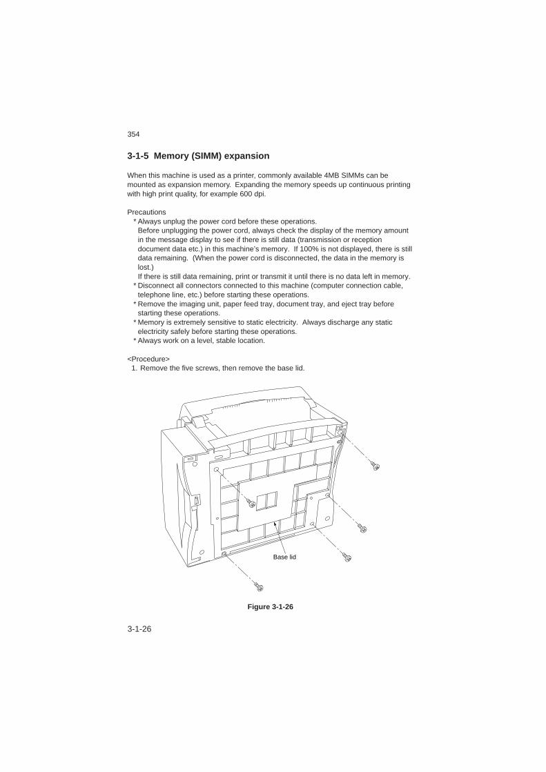
3-1-26
354
3-1-5 Memory (SIMM) expansion
When this machine is used as a printer, commonly available 4MB SIMMs can bemounted as expansion memory. Expanding the memory speeds up continuous printingwith high print quality, for example 600 dpi.
Precautions * Always unplug the power cord before these operations.
Before unplugging the power cord, always check the display of the memory amountin the message display to see if there is still data (transmission or receptiondocument data etc.) in this machine’s memory. If 100% is not displayed, there is stilldata remaining. (When the power cord is disconnected, the data in the memory islost.)If there is still data remaining, print or transmit it until there is no data left in memory.
* Disconnect all connectors connected to this machine (computer connection cable,telephone line, etc.) before starting these operations.
* Remove the imaging unit, paper feed tray, document tray, and eject tray beforestarting these operations.
* Memory is extremely sensitive to static electricity. Always discharge any staticelectricity safely before starting these operations.
* Always work on a level, stable location.
<Procedure> 1. Remove the five screws, then remove the base lid.
Base lid
Figure 3-1-26

3-1-27
354
2. Firmly insert the connector for the expansion memory into CN 19 (expansionmemory connector) on the control PCB of this machine.
* Make sure that the expansion memory is securely fastened by the clips on bothends of the expansion memory connector.
Expansion memory (SIMM) CN19
(expansion memory connector)
Figure 3-1-27
3. Install the base lid in its original position on the main body of the machine. 4. Install the units (imaging unit, paper feed tray, etc.) removed from the main body of
the machine back in their original positions on the main body of the machine. 5. Connect the disconnected connectors, telephone line, etc. in their original positions. 6. Connect the power cord to the power connector as it was before removal.
354-1

3-2-1
354
3-2-1 Outline of service mode and test mode
* When entering the password,unless each key is pressed within 2 sec or any other key is pressed, the machine will re-turn to the user mode at that time.
TEST MODE
USER MODE
Press the Stop/Reset key.
Press 0 key.
Press the Function key.
Press 2 key.
Press the Function key.
Press 3 key.
Press 1 key.
Press the * key
Press the Enter key.
Press the # key.
Power turn off?no yes
Press the Function keyseven times.
SERVICE MODE
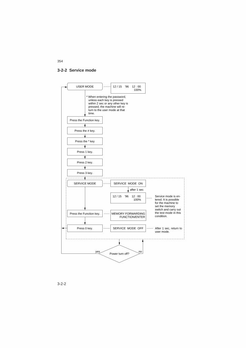
3-2-2
354
3-2-2 Service mode
* When entering the password, unless each key is pressed within 2 sec or any other key is pressed, the machine will re-turn to the user mode at that time.
SERVICE MODE
USER MODE
Press 0 key.
Press the Function key.
Press 2 key.
Press the Function key.
12 / 15 '96 12 : 00 100%
·········
12 / 15 '96 12 : 00 100%
·········
MEMORY FORWARDINGFUNCTION/ENTER
·······
········ ········
Service mode is en-tered. It is possible for the machine to set the memory switch and carry out the test mode in this condition.
·······
After 1 sec, return to user mode.
Press 3 key.
SERVICE MODE ON
SERVICE MODE OFF
Press 1 key.
Press the * key
Press the # key.
Power turn off?noyes
after 1 sec
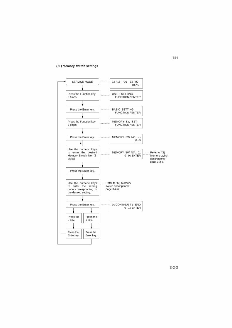
3-2-3
354
Use the numeric keys to enter the desired Memory Switch No. (2-digits)
Use the numeric keys to enter the setting code corresponding to the desired setting.
Press the Enter key.
Press the Enter key.
Press the Enter key.
Press the Enter key.
Press the Function key6 times.
Press the Function key7 times.
SERVICE MODE
MEMORY SW SET FUNCTION / ENTER
12 / 15 '96 12 : 00 100%
·············
MEMORY SW NO. : 01 0 - 9 / ENTER·············
0 : CONTINUE / 1 : END 0 - 1 / ENTER
·············
········
Refer to "(3) Memory switch descriptions", page 3-2-6.
·········
USER SETTING FUNCTION / ENTER
·············
·············
MEMORY SW NO. : - - 0 - 9
·············
·············
Refer to "(3) Memory switch descriptions", page 3-2-6.
BASIC SETTING FUNCTION / ENTER
Press the 1 key.
Press the 0 key.
Press theEnter key.
Press theEnter key.
( 1 ) Memory switch settings
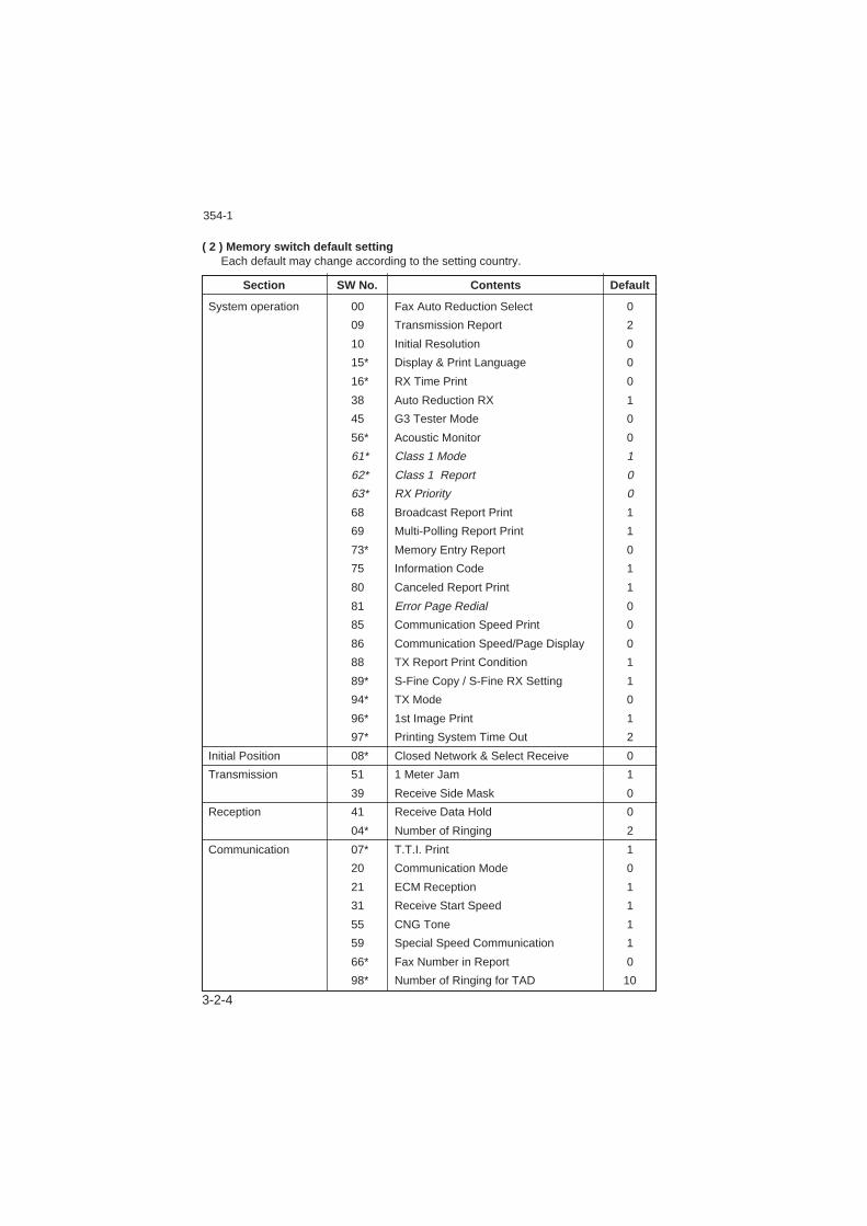
3-2-4
354
( 2 ) Memory switch default settingEach default may change according to the setting country.
System operation 00 Fax Auto Reduction Select 0
09 Transmission Report 2
10 Initial Resolution 0
15* Display & Print Language 0
16* RX Time Print 0
38 Auto Reduction RX 1
45 G3 Tester Mode 0
56* Acoustic Monitor 0
61* Class 1 Mode 1
62* Class 1 Report 0
63* RX Priority 0
68 Broadcast Report Print 1
69 Multi-Polling Report Print 1
73* Memory Entry Report 0
75 Information Code 1
80 Canceled Report Print 1
81 Error Page Redial 0
85 Communication Speed Print 0
86 Communication Speed/Page Display 0
88 TX Report Print Condition 1
89* S-Fine Copy / S-Fine RX Setting 1
94* TX Mode 0
96* 1st Image Print 1
97* Printing System Time Out 2
Initial Position 08* Closed Network & Select Receive 0
Transmission 51 1 Meter Jam 1
39 Receive Side Mask 0
Reception 41 Receive Data Hold 0
04* Number of Ringing 2
Communication 07* T.T.I. Print 1
20 Communication Mode 0
21 ECM Reception 1
31 Receive Start Speed 1
55 CNG Tone 1
59 Special Speed Communication 1
66* Fax Number in Report 0
98* Number of Ringing for TAD 10
Section SW No. Contents Default
354-1
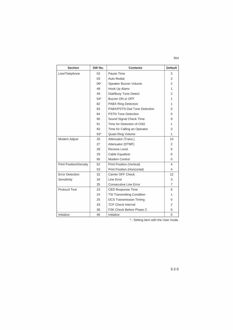
3-2-5
354
Line/Telephone 02 Pause Time 3
03 Auto Redial 2
06* Speaker Buzzer Volume 2
48 Hook Up Alarm 1
49 Dial/Busy Tone Detect 2
54* Buzzer ON or OFF 1
82 PABX Ring Detection 1
83 PABX/PSTN Dial Tone Detection 0
84 PSTN Tone Detection 0
90 Sound Signal Check TIme 9
91 Time for Detection of CNG 1
92 Time for Calling an Operator 3
93* Quasi Ring Volume 1
Modem Adjust 26 Attenuator (Trans.) 10
27 Attenuator (DTMF) 2
28 Receive Level 6
29 Cable Equalizer 0
95 Modem Control 0
Print Position/Density 52 Print Position (Vertical) 4
53 Print Position (Horizontal) 4
Error Detection 32 Carrier OFF Check 12
Sensitivity 34 Line Error 3
35 Consecutive Line Error 7
Protocol Test 23 CED Response Time 6
24 TSI Transmitting Condition 1
25 DCS Transmission Timing 0
33 TCF Check Interval 2
36 FSK Check Before Phase C 6
Initialize 46 Initialize 0
Section SW No. Contents Default
* : Setting item with the User mode.
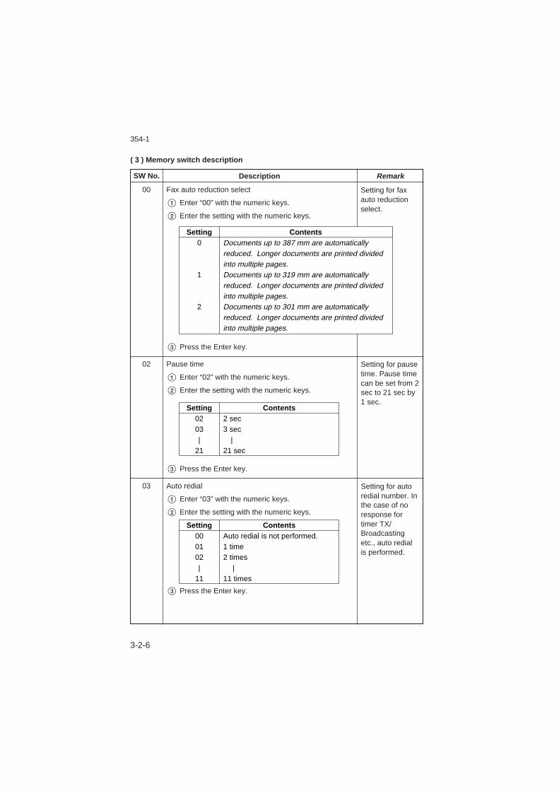
3-2-6
354
00 Fax auto reduction select
1 Enter “00” with the numeric keys.
2 Enter the setting with the numeric keys.
3 Press the Enter key.
02 Pause time
1 Enter “02” with the numeric keys.
2 Enter the setting with the numeric keys.
3 Press the Enter key.
03 Auto redial
1 Enter “03” with the numeric keys.
2 Enter the setting with the numeric keys.
3 Press the Enter key.
Setting for faxauto reductionselect.
Setting for pausetime. Pause timecan be set from 2sec to 21 sec by1 sec.
Setting for autoredial number. Inthe case of noresponse fortimer TX/Broadcastingetc., auto redialis performed.
( 3 ) Memory switch description
SW No. Description Remark
Setting Contents0
1
2
Documents up to 387 mm are automatically reduced. Longer documents are printed divided into multiple pages.Documents up to 319 mm are automatically reduced. Longer documents are printed divided into multiple pages.Documents up to 301 mm are automatically reduced. Longer documents are printed divided into multiple pages.
Setting Contents0203|
21
2 sec3 sec
|21 sec
Setting Contents000102|
11
Auto redial is not performed.1 time2 times
|11 times
354-1

3-2-7
354
04 Number of ringing
1 Enter “04” with the numeric keys.
2 Enter the setting with the numeric keys.
3 Press the Enter key.
06 Speaker buzzer volume
1 Enter “06” with the numeric keys.
2 Enter the setting with the numeric keys.
3 Press the Enter key.
Setting fornumber ofringing. In thecase of autoreceive mode,number of ringingto received stateis set. Number ofringing is setfrom 1 to 11 by 1step.
Setting forspeaker volume.
SW No. Description Remark
Setting Contents0102|
11
1 time2 times
|11 times
Setting Contents123
SmallNormalBig
354-1
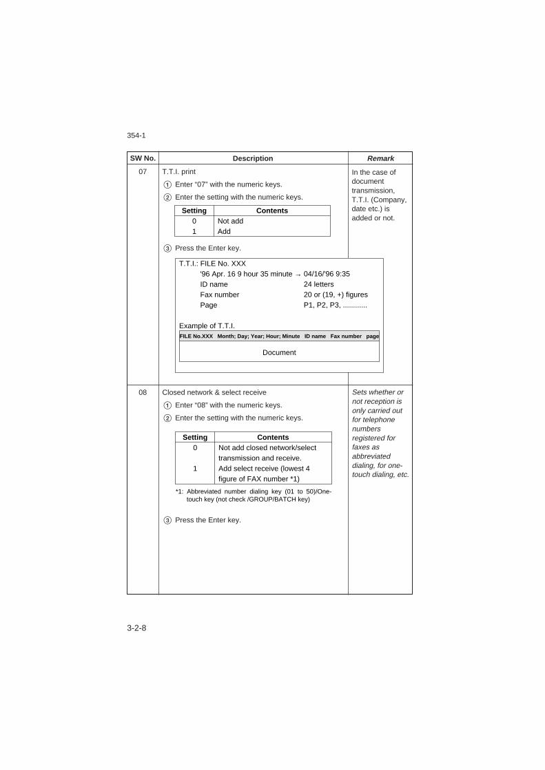
3-2-8
354
07 T.T.I. print
1 Enter “07” with the numeric keys.
2 Enter the setting with the numeric keys.
3 Press the Enter key.
08 Closed network & select receive
1 Enter “08” with the numeric keys.
2 Enter the setting with the numeric keys.
3 Press the Enter key.
In the case ofdocumenttransmission,T.T.I. (Company,date etc.) isadded or not.
Sets whether ornot reception isonly carried outfor telephonenumbersregistered forfaxes asabbreviateddialing, for one-touch dialing, etc.
SW No. Description Remark
Setting Contents01
Not addAdd
T.T.I.: FILE No. XXX'96 Apr. 16 9 hour 35 minute →ID nameFax number Page
Example of T.T.I.
04/16/'96 9:3524 letters20 or (19, +) figuresP1, P2, P3, ............
FILE No.XXX Month; Day; Year; Hour; Minute ID name Fax number page
Document
*1: Abbreviated number dialing key (01 to 50)/One-touch key (not check /GROUP/BATCH key)
Setting Contents0
1
Not add closed network/selecttransmission and receive.Add select receive (lowest 4figure of FAX number *1)
354-1
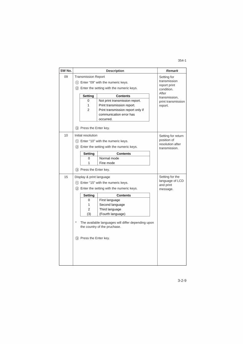
3-2-9
354
09 Transmission Report
1 Enter “09” with the numeric keys.
2 Enter the setting with the numeric keys.
3 Press the Enter key.
10 Initial resolution
1 Enter “10” with the numeric keys.
2 Enter the setting with the numeric keys.
3 Press the Enter key.
15 Display & print language
1 Enter “15” with the numeric keys.
2 Enter the setting with the numeric keys.
* The available languages will differ depending uponthe country of the pruchase.
3 Press the Enter key.
Setting fortransmissionreport printcondition.Aftertransmission,print transmissionreport.
Setting for returnposition ofresolution aftertransmission.
SW No. Description Remark
Setting Contents012
Not print transmission report.Print transmission report.Print transmission report only if communication error has occurred.
Setting Contents01
Normal modeFine mode
Setting Contents012
(3)
First languageSecond languageThird language(Fourth language)
Setting for thelanguage of LCDand printmessage.
354-1
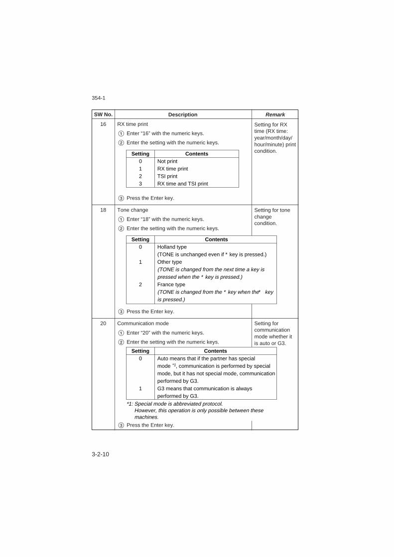
3-2-10
354
16 RX time print
1 Enter “16” with the numeric keys.
2 Enter the setting with the numeric keys.
3 Press the Enter key.
18 Tone change
1 Enter “18” with the numeric keys.
2 Enter the setting with the numeric keys.
3 Press the Enter key.
20 Communication mode
1 Enter “20” with the numeric keys.
2 Enter the setting with the numeric keys.
3 Press the Enter key.
Setting for RXtime (RX time:year/month/day/hour/minute) printcondition.
Setting for tonechangecondition.
SW No. Description Remark
Setting Contents0123
Not printRX time printTSI printRX time and TSI print
Setting Contents0
1
2
Holland type(TONE is unchanged even if ∗ key is pressed.)Other type(TONE is changed from the next time a key is pressed when the key is pressed.)France type(TONE is changed from the key when the key is pressed.)
∗
∗ ∗
Setting forcommunicationmode whether itis auto or G3.
Setting Contents0
1
*1: Special mode is abbreviated protocol.However, this operation is only possible between these machines.
Auto means that if the partner has special mode *1, communication is performed by special mode, but it has not special mode, communicationperformed by G3.G3 means that communication is alwaysperformed by G3.
354-1
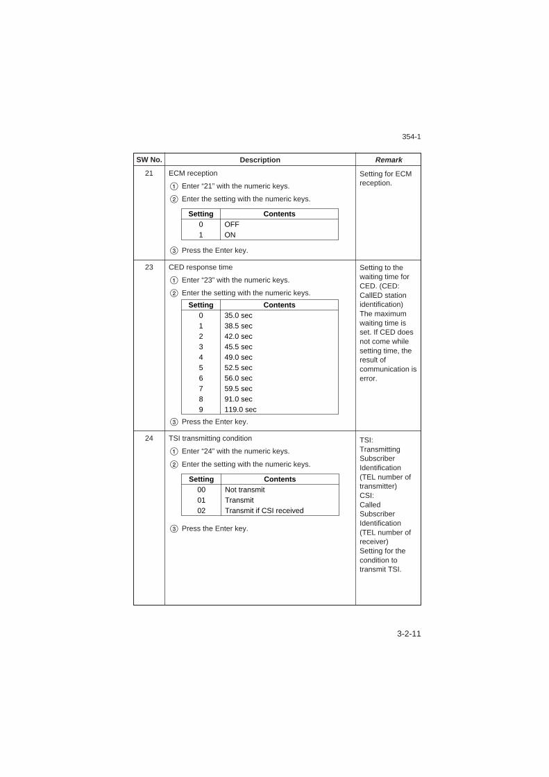
3-2-11
354
21 ECM reception
1 Enter “21” with the numeric keys.
2 Enter the setting with the numeric keys.
3 Press the Enter key.
23 CED response time
1 Enter “23” with the numeric keys.
2 Enter the setting with the numeric keys.
3 Press the Enter key.
24 TSI transmitting condition
1 Enter “24” with the numeric keys.
2 Enter the setting with the numeric keys.
3 Press the Enter key.
Setting for ECMreception.
Setting to thewaiting time forCED. (CED:CallED stationidentification)The maximumwaiting time isset. If CED doesnot come whilesetting time, theresult ofcommunication iserror.
SW No. Description Remark
TSI:TransmittingSubscriberIdentification(TEL number oftransmitter)CSI:CalledSubscriberIdentification(TEL number ofreceiver)Setting for thecondition totransmit TSI.
Setting Contents01
OFFON
Setting Contents0123456789
35.0 sec38.5 sec42.0 sec45.5 sec49.0 sec52.5 sec56.0 sec59.5 sec91.0 sec119.0 sec
Setting Contents000102
Not transmitTransmitTransmit if CSI received
354-1

3-2-12
354
25 DCS transmission timing
1 Enter “25” with the numeric keys.
2 Enter the setting with the numeric keys.
3 Press the Enter key.
26 Attenuator (trans.)
1 Enter “26” with the numeric keys.
2 Enter the setting with the numeric keys.
3 Press the Enter key.
27 Attenuator (DTMF.)
1 Enter “27” with the numeric keys.
2 Enter the setting with the numeric keys.
3 Press the Enter key.
DCS:Digital CommandSignal (DigitalRecognitionSignal ofstandard facilityof transmitter)DIS:DigitalIdentificationSignal (DigitalRecognitionSignal ofstandard facilityof receiver)Setting for thecondition totransmit DCS.
Setting fortransmittingpower level ofFAX signal. (by 1dBm step)
SW No. Description Remark
Setting fortransmittingpower level ofDTMF signal. (by1 dBm step)
Setting Contents01
Response to first DIS.Response to second DIS.
Setting Contents00|
20
0 dBm|
–20 dBm
Setting Contents00|
20
0 dBm|
–20 dBm
354-1

3-2-13
354
28 Receive level
1 Enter “28” with the numeric keys.
2 Enter the setting with the numeric keys.
3 Press the Enter key.
29 Cable equalizer
1 Enter “29” with the numeric keys.
2 Enter the setting with the numeric keys.
3 Press the Enter key.
31 Receive start speed
1 Enter “31” with the numeric keys.
2 Enter the setting with the numeric keys.
3 Press the Enter key.
32 Carrier off check (carrior interval of RX data)
1 Enter “32” with the numeric keys.
2 Enter the setting with the numeric keys.
3 Press the Enter key.
Setting forreceive level ofFAX signal. (by 1dBm step)If FAX signalwhich is lowerthan setting levelis received, it isnot recognizedas FAX signal.
Setting for cableequalizer whichrectifies thecharacteristics ofthe distance fromsetting place toswitching office.
SW No. Description Remark
Setting forreceive startspeed of modem.
Setting Contents01|
11
–38 dBm|
–48 dBm
Setting Contents01
0 km7.2 km
Setting Contents01
4800 bps14400 bps
Setting Contents0001|
12
0 sec (by 0.5 sec step)0.5 sec
|6 sec
Setting for carrieroff check time. Ifcarrier signal iscut off duringmore than settingtime, only low-speed commandsignal is watchedout up to total 6seconds.
354-1
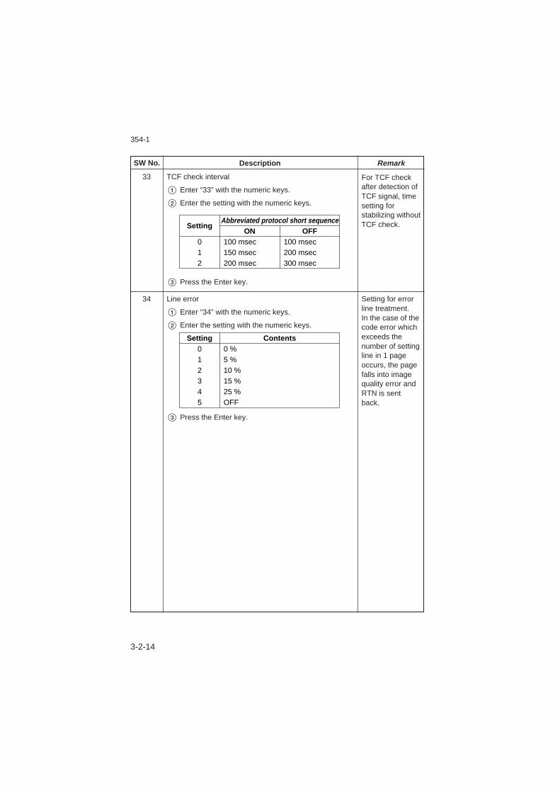
3-2-14
354
33 TCF check interval
1 Enter “33” with the numeric keys.
2 Enter the setting with the numeric keys.
3 Press the Enter key.
34 Line error
1 Enter “34” with the numeric keys.
2 Enter the setting with the numeric keys.
3 Press the Enter key.
For TCF checkafter detection ofTCF signal, timesetting forstabilizing withoutTCF check.
Setting for errorline treatment.In the case of thecode error whichexceeds thenumber of settingline in 1 pageoccurs, the pagefalls into imagequality error andRTN is sentback.
SW No. Description Remark
SettingON
Abbreviated protocol short sequence
012
100 msec150 msec200 msec
100 msec200 msec300 msec
OFF
Setting Contents012345
0 %5 %10 %15 %25 %OFF
354-1
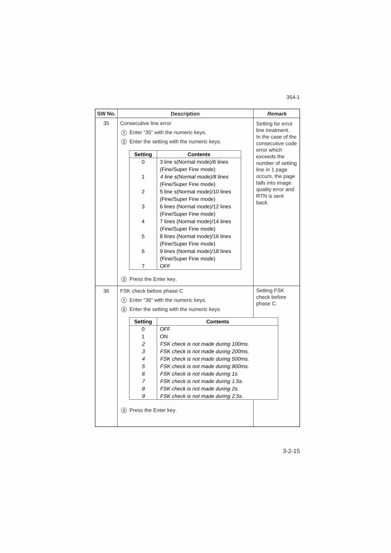
3-2-15
354
35 Consecutive line error
1 Enter “35” with the numeric keys.
2 Enter the setting with the numeric keys.
3 Press the Enter key.
36 FSK check before phase C
1 Enter “36” with the numeric keys.
2 Enter the setting with the numeric keys.
3 Press the Enter key.
Setting for errorline treatment.In the case of theconsecutive codeerror whichexceeds thenumber of settingline in 1 pageoccurs, the pagefalls into imagequality error andRTN is sentback.
Setting FSKcheck beforephase C.
SW No. Description Remark
Setting Contents0
1
2
3
4
5
6
7
3 line s(Normal mode)/6 lines(Fine/Super Fine mode)4 line s(Normal mode)/8 lines(Fine/Super Fine mode)5 line s(Normal mode)/10 lines(Fine/Super Fine mode)6 lines (Normal mode)/12 lines(Fine/Super Fine mode)7 lines (Normal mode)/14 lines(Fine/Super Fine mode)8 lines (Normal mode)/16 lines(Fine/Super Fine mode)9 lines (Normal mode)/18 lines(Fine/Super Fine mode)OFF
Setting Contents0123456789
OFFONFSK check is not made during 100ms.FSK check is not made during 200ms.FSK check is not made during 500ms.FSK check is not made during 800ms.FSK check is not made during 1s.FSK check is not made during 1.5s.FSK check is not made during 2s.FSK check is not made during 2.5s.
354-1
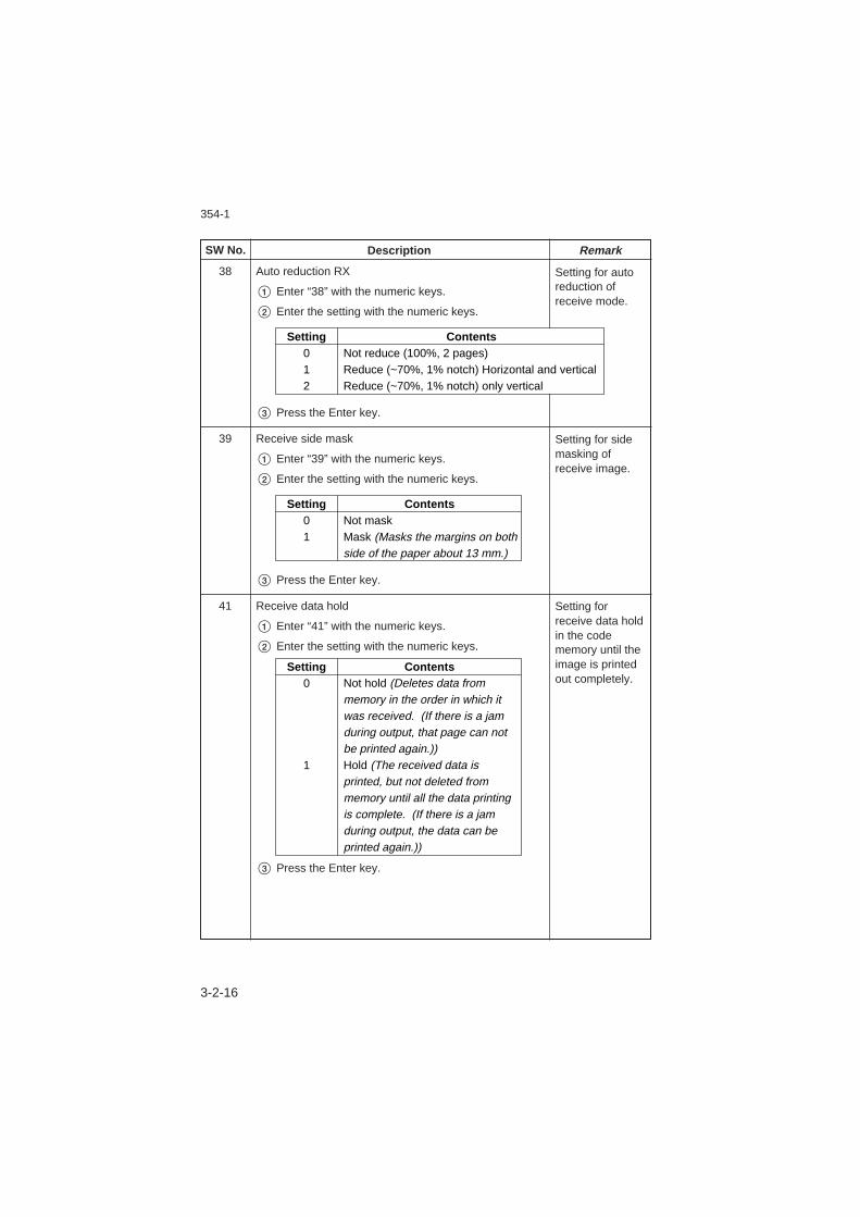
3-2-16
354
38 Auto reduction RX
1 Enter “38” with the numeric keys.
2 Enter the setting with the numeric keys.
3 Press the Enter key.
39 Receive side mask
1 Enter “39” with the numeric keys.
2 Enter the setting with the numeric keys.
3 Press the Enter key.
41 Receive data hold
1 Enter “41” with the numeric keys.
2 Enter the setting with the numeric keys.
3 Press the Enter key.
Setting for autoreduction ofreceive mode.
Setting for sidemasking ofreceive image.
SW No. Description Remark
Setting Contents012
Not reduce (100%, 2 pages)Reduce (~70%, 1% notch) Horizontal and verticalReduce (~70%, 1% notch) only vertical
Setting Contents01
Not maskMask (Masks the margins on both side of the paper about 13 mm.)
Setting Contents0
1
Not hold (Deletes data from memory in the order in which it was received. (If there is a jam during output, that page can not be printed again.))Hold (The received data is printed, but not deleted from memory until all the data printing is complete. (If there is a jam during output, the data can be printed again.))
Setting forreceive data holdin the codememory until theimage is printedout completely.
354-1

3-2-17
354
45 G3 tester mode
1 Enter “45” with the numeric keys.
2 Enter the setting with the numeric keys.
3 Press the Enter key.
46 Initialize
1 Enter “46” with the numeric keys.
2 Enter the setting with the numeric keys.
3 Press the Enter key.
48 Hook up alarm
1 Enter “48” with the numeric keys.
2 Enter the setting with the numeric keys.
3 Press the Enter key.
Setting for FAXdata initialize.
Setting for hookup alarm whichindicates internal/external handsetis hung on.
SW No. Description Remark
Setting Contents012
3456
All data clear.File *1/Command data clearAbbreviated number dialing key/One-touch key/P key *2/Batch key data clearReport data clearMemory switch table data clearPrinter counter data clearActivity report TX/RX count clear
*1: Document data stored in memory*2: Program key
Setting Contents01
Not alarmAlarm
Setting Contents012
Not printPrint after every communication.Print only if communication error has occurred.
Setting for G3report printingaftercommunication.
354-1

3-2-18
354
49 Dial/busy tone detect (Line standard applicationpending)
1 Enter “49” with the numeric keys.
2 Enter the setting with the numeric keys.
3 Press the Enter key.
51 1 meter jam
1 Enter “51” with the numeric keys.
2 Enter the setting with the numeric keys.
3 Press the Enter key.
52 Print position (vertical)
1 Enter “52” with the numeric keys.
2 Enter the setting with the numeric keys.
3 Press the Enter key.
Setting for 1meter jam whichmeans ifdocumentexceeds 1 m, 2m, 3 m jam isjudged.
Setting forvertical positionof print start. (by1mm step)(see page 3-3-44)
SW No. Description Remark
Setting Contents0123
OFF1 m2 m3 m
Setting Contents01|5|8
0 mm1 mm
|5 mm
|8 mm
Setting Contents012
Busy tone detection on, other tone detection offObserve the regulationAll tone detection off
Setting for dial orbusy tonedetection.
354-1
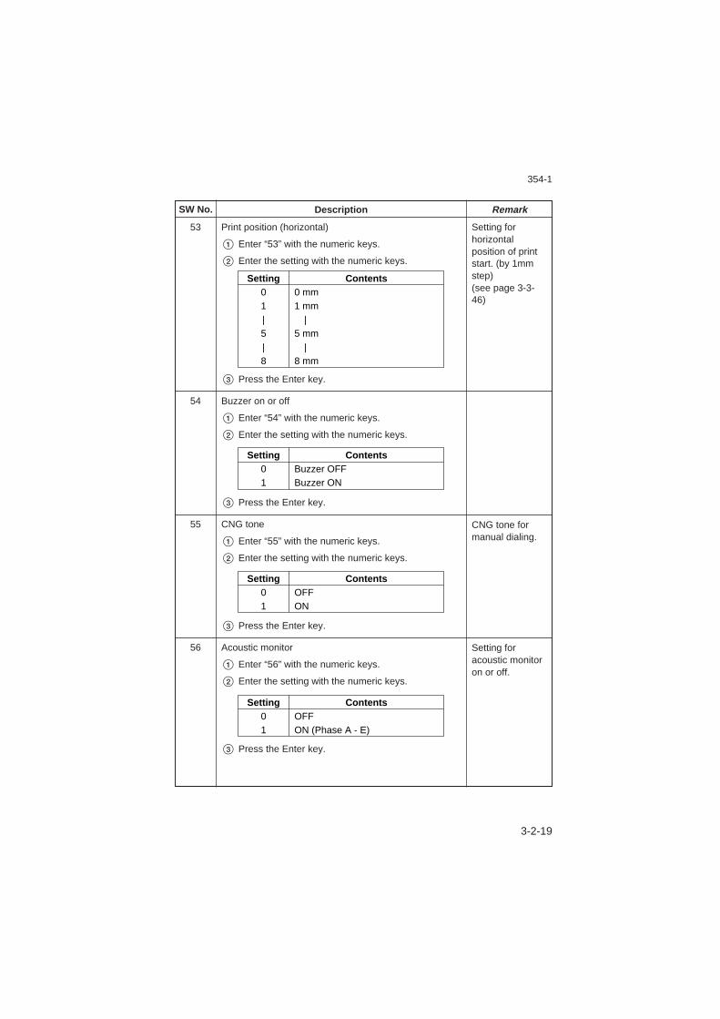
3-2-19
354
53 Print position (horizontal)
1 Enter “53” with the numeric keys.
2 Enter the setting with the numeric keys.
3 Press the Enter key.
54 Buzzer on or off
1 Enter “54” with the numeric keys.
2 Enter the setting with the numeric keys.
3 Press the Enter key.
55 CNG tone
1 Enter “55” with the numeric keys.
2 Enter the setting with the numeric keys.
3 Press the Enter key.
56 Acoustic monitor
1 Enter “56” with the numeric keys.
2 Enter the setting with the numeric keys.
3 Press the Enter key.
CNG tone formanual dialing.
SW No. Description Remark
Setting foracoustic monitoron or off.
Setting Contents01
Buzzer OFFBuzzer ON
Setting Contents01
OFFON
Setting Contents01
OFFON (Phase A - E)
Setting forhorizontalposition of printstart. (by 1mmstep)(see page 3-3-46)
Setting Contents01|5|8
0 mm1 mm
|5 mm
|8 mm
354-1

3-2-20
354
This page is intentionally left blank.
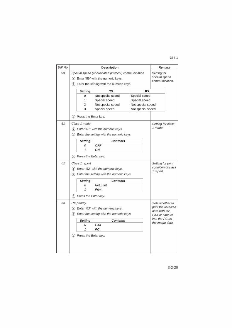
3-2-21
354
59 Special speed (abbreviated protocol) communication
1 Enter “59” with the numeric keys.
2 Enter the setting with the numeric keys.
3 Press the Enter key.
61 Class 1 mode
1 Enter “61” with the numeric keys.
2 Enter the setting with the numeric keys.
3 Press the Enter key.
62 Class 1 report
1 Enter “62” with the numeric keys.
2 Enter the setting with the numeric keys.
3 Press the Enter key.
63 RX priority
1 Enter “63” with the numeric keys.
2 Enter the setting with the numeric keys.
3 Press the Enter key.
Setting for class1 mode.
Setting for printcondition of class1 report.
SW No. Description Remark
Sets whether toprint the receiveddata with theFAX or captureinto the PC asthe image data.
Setting Contents01
OFFON
Setting Contents01
Not printPrint
Setting Contents01
FAXPC
Setting TX0123
Not special speedSpecial speedNot special speedSpecial speed
Special speedSpecial speedNot special speedNot special speed
RX
Setting forspecial speedcommunication.
3-2-20
354-1
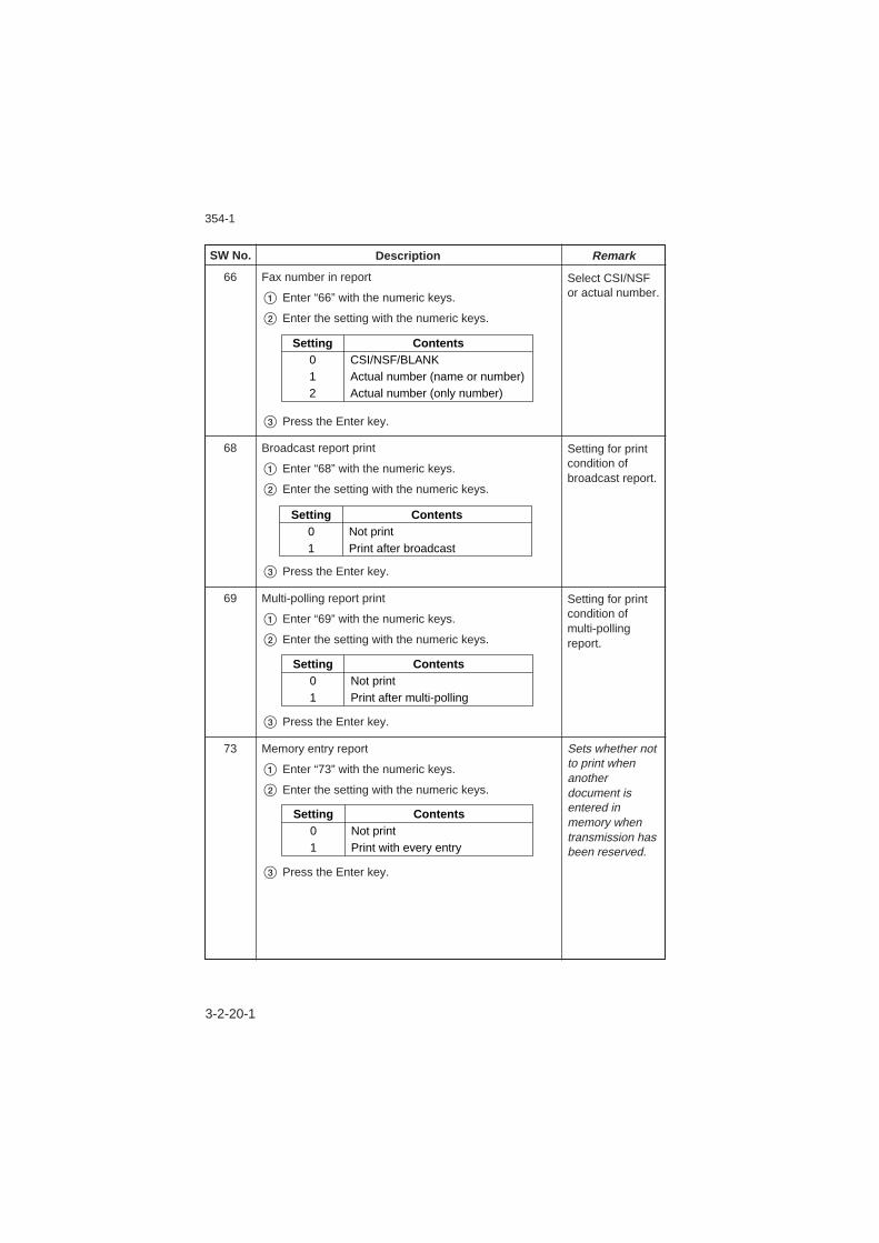
3-2-22
354
66 Fax number in report
1 Enter “66” with the numeric keys.
2 Enter the setting with the numeric keys.
3 Press the Enter key.
68 Broadcast report print
1 Enter “68” with the numeric keys.
2 Enter the setting with the numeric keys.
3 Press the Enter key.
69 Multi-polling report print
1 Enter “69” with the numeric keys.
2 Enter the setting with the numeric keys.
3 Press the Enter key.
73 Memory entry report
1 Enter “73” with the numeric keys.
2 Enter the setting with the numeric keys.
3 Press the Enter key.
Select CSI/NSFor actual number.
Setting for printcondition ofbroadcast report.
SW No. Description Remark
Setting for printcondition ofmulti-pollingreport.
Setting Contents012
CSI/NSF/BLANKActual number (name or number)Actual number (only number)
Setting Contents01
Not printPrint after broadcast
Setting Contents01
Not printPrint after multi-polling
Setting Contents01
Not printPrint with every entry
Sets whether notto print whenanotherdocument isentered inmemory whentransmission hasbeen reserved.
354-1
3-2-20-1
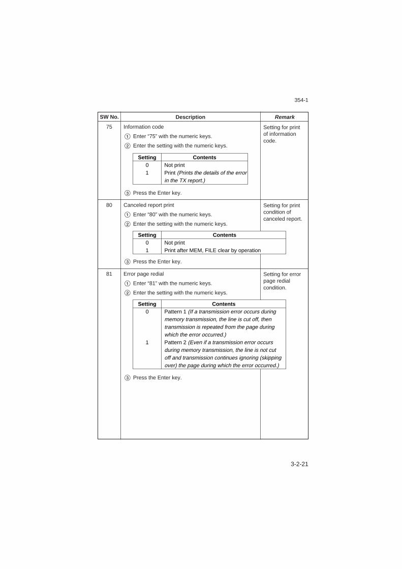
3-2-23
354
75 Information code
1 Enter “75” with the numeric keys.
2 Enter the setting with the numeric keys.
3 Press the Enter key.
80 Canceled report print
1 Enter “80” with the numeric keys.
2 Enter the setting with the numeric keys.
3 Press the Enter key.
81 Error page redial
1 Enter “81” with the numeric keys.
2 Enter the setting with the numeric keys.
3 Press the Enter key.
Setting for printof informationcode.
Setting for printcondition ofcanceled report.
SW No. Description Remark
Setting for errorpage redialcondition.
Setting Contents01
Not printPrint (Prints the details of the error in the TX report.)
Setting Contents01
Not printPrint after MEM, FILE clear by operation
Setting Contents0
1
Pattern 1 (If a transmission error occurs during memory transmission, the line is cut off, then transmission is repeated from the page during which the error occurred.)Pattern 2 (Even if a transmission error occurs during memory transmission, the line is not cut off and transmission continues ignoring (skipping over) the page during which the error occurred.)
354-1
3-2-21
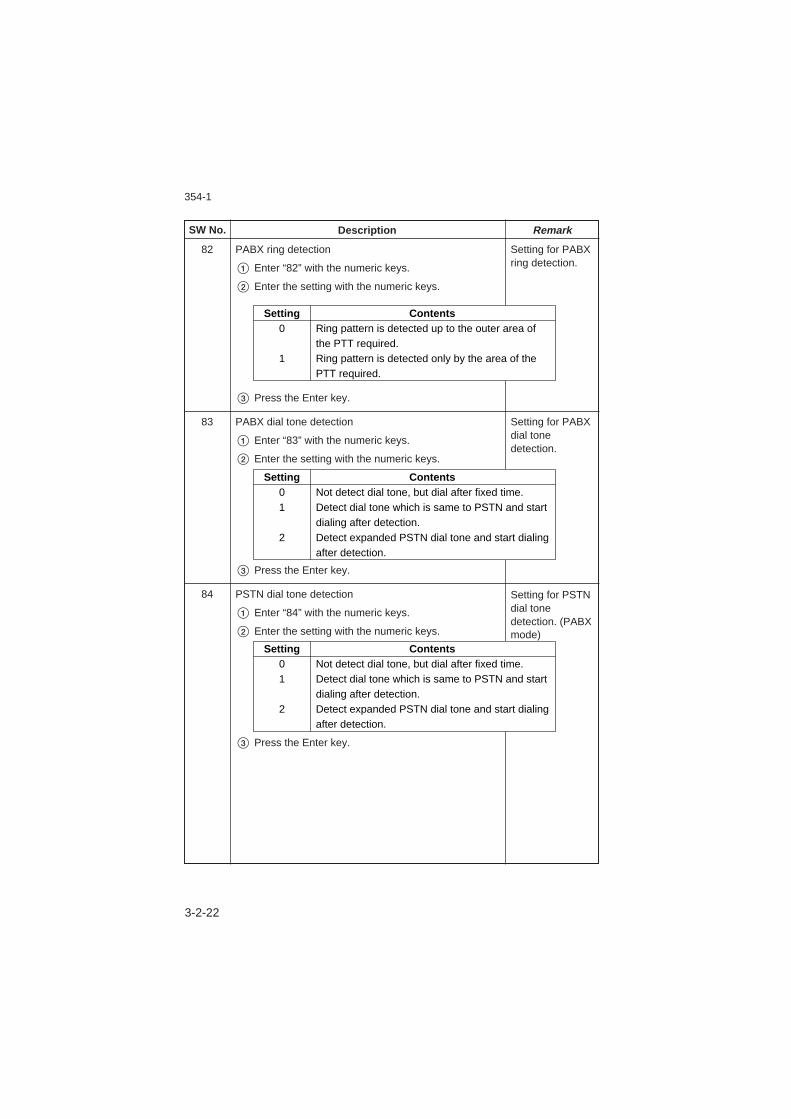
3-2-24
354
82 PABX ring detection
1 Enter “82” with the numeric keys.
2 Enter the setting with the numeric keys.
3 Press the Enter key.
83 PABX dial tone detection
1 Enter “83” with the numeric keys.
2 Enter the setting with the numeric keys.
3 Press the Enter key.
84 PSTN dial tone detection
1 Enter “84” with the numeric keys.
2 Enter the setting with the numeric keys.
3 Press the Enter key.
Setting for PABXdial tonedetection.
Setting for PSTNdial tonedetection. (PABXmode)
SW No. Description Remark
Setting Contents01
2
Not detect dial tone, but dial after fixed time.Detect dial tone which is same to PSTN and startdialing after detection.Detect expanded PSTN dial tone and start dialingafter detection.
Setting Contents01
2
Not detect dial tone, but dial after fixed time.Detect dial tone which is same to PSTN and startdialing after detection.Detect expanded PSTN dial tone and start dialingafter detection.
Setting Contents0
1
Ring pattern is detected up to the outer area ofthe PTT required.Ring pattern is detected only by the area of thePTT required.
Setting for PABXring detection.
354-1
3-2-22
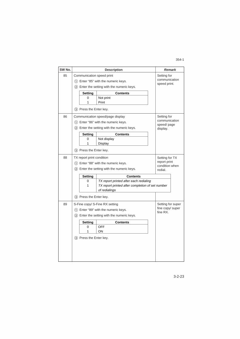
3-2-25
354
85 Communication speed print
1 Enter “85” with the numeric keys.
2 Enter the setting with the numeric keys.
3 Press the Enter key.
86 Communication speed/page display
1 Enter “86” with the numeric keys.
2 Enter the setting with the numeric keys.
3 Press the Enter key.
88 TX report print condition
1 Enter “88” with the numeric keys.
2 Enter the setting with the numeric keys.
3 Press the Enter key.
89 S-Fine copy/ S-Fine RX setting
1 Enter “89” with the numeric keys.
2 Enter the setting with the numeric keys.
3 Press the Enter key.
Setting forcommunicationspeed/ pagedisplay.
Setting for TXreport printcondition whenredial.
SW No. Description Remark
Setting for superfine copy/ superfine RX.
Setting Contents01
Not displayDisplay
Setting Contents01
TX report printed after each redialingTX report printed after completion of set number of redialings
Setting Contents01
OFFON
Setting forcommunicationspeed print.
Setting Contents01
Not printPrint
354-1
3-2-23
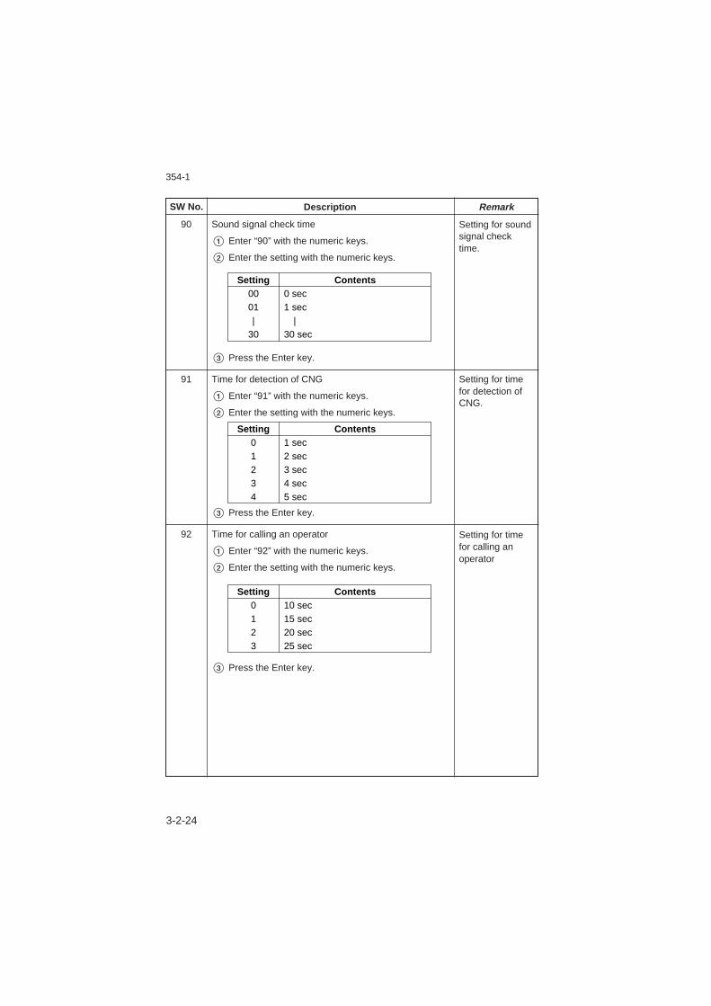
3-2-26
354
90 Sound signal check time
1 Enter “90” with the numeric keys.
2 Enter the setting with the numeric keys.
3 Press the Enter key.
91 Time for detection of CNG
1 Enter “91” with the numeric keys.
2 Enter the setting with the numeric keys.
3 Press the Enter key.
92 Time for calling an operator
1 Enter “92” with the numeric keys.
2 Enter the setting with the numeric keys.
3 Press the Enter key.
Setting for timefor detection ofCNG.
Setting for timefor calling anoperator
SW No. Description Remark
Setting Contents01234
1 sec2 sec3 sec4 sec5 sec
Setting Contents0123
10 sec15 sec20 sec25 sec
Setting for soundsignal checktime.
Setting Contents0001|
30
0 sec1 sec
|30 sec
354-1
3-2-24

3-2-27
354
93 Quasi ring volume
1 Enter “93” with the numeric keys.
2 Enter the setting with the numeric keys.
3 Press the Enter key.
94 TX mode
1 Enter “94” with the numeric keys.
2 Enter the setting with the numeric keys.
3 Press the Enter key.
95 Modem control
1 Enter “95” with the numeric keys.
2 Enter the setting with the numeric keys.
3 Press the Enter key.
96 1st image print
1 Enter “96” with the numeric keys.
2 Enter the setting with the numeric keys.
3 Press the Enter key.
Setting for TXmode.
Setting formodem control.
SW No. Description Remark
Setting for 1stimage print(transmissionreport).
Setting Contents01
ADF TX (Direct transmission)Memory TX
Setting Contents01
OFF (Not print)ON (Print)
Setting Contents012
SmallNormalBig
Setting for quasiring volume.
354-1
3-2-25
Setting Contents0123
Equalizer freeze *1 OFF/Carrier checkEqualizer freeze ON/Carrier checkEqualizer freeze OFF/EQM checkEqualizer freeze ON/EQM check
*1: The equalizer freeze corrects for carrier data distortion and retains that correction value.
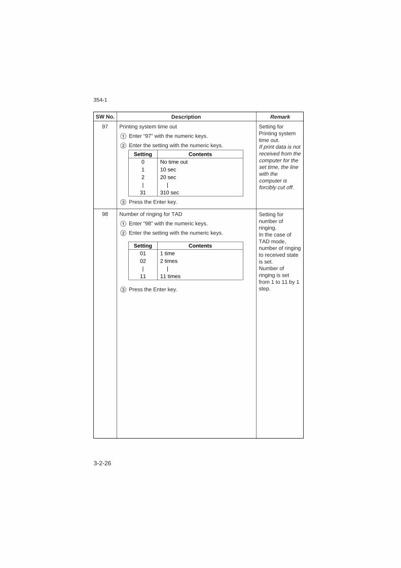
3-2-28
354
97 Printing system time out
1 Enter “97” with the numeric keys.
2 Enter the setting with the numeric keys.
3 Press the Enter key.
98 Number of ringing for TAD
1 Enter “98” with the numeric keys.
2 Enter the setting with the numeric keys.
3 Press the Enter key.
Setting fornumber ofringing.In the case ofTAD mode,number of ringingto received stateis set.Number ofringing is setfrom 1 to 11 by 1step.
SW No. Description Remark
Setting Contents0102|
11
1 time2 times
|11 times
Setting forPrinting systemtime out.If print data is notreceived from thecomputer for theset time, the linewith thecomputer isforcibly cut off.
Setting Contents012|
31
No time out10 sec20 sec
|310 sec
354-1
3-2-26
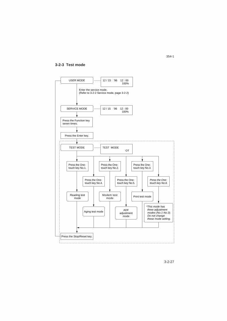
3-2-29
354
3-2-3 Test mode
Enter the service mode.(Refer to 3-2-2 Service mode, page 3-2-2)
SERVICE MODE
TEST MODE
USER MODE
Press the Stop/Reset key.
Press the Enter key.
12 / 15 '96 12 : 00 100%
Press the Function keyseven times.
·········
12 / 15 '96 12 : 00 100%
·········
TEST MODE OT
·········
Press the One-touch key No.1.
Press the One-touch key No.2.
Press the One-touch key No.4.
Press the One-touch key No.5.
Press the One-touch key No.3.
Reading test mode
Modem test mode
Aging test mode ADFadjustment
mode
Press the One-touch key No.6.
*This mode has three adjustment modes (No.1-No.3).Do not change these mode setting.
Print test mode
354-1
3-2-27

3-2-30
354
Press the Enter key.
Press the Stop/Reset key.
Press the Function keyseven times.
Press the One-touch key No.1.
SCANNER ON
TEST MODE
Reading test mode
SERVICE MODE
Press the Stop/Reset key.
TEST MODE OT
SCANNER LED ON
·············
·············
·············
* The exposure lamp(LED) of the contact im-age sensor lights.
( 1 ) Reading test mode* In this mode, check the contact image sensor (CIS) operation.
3-2-28
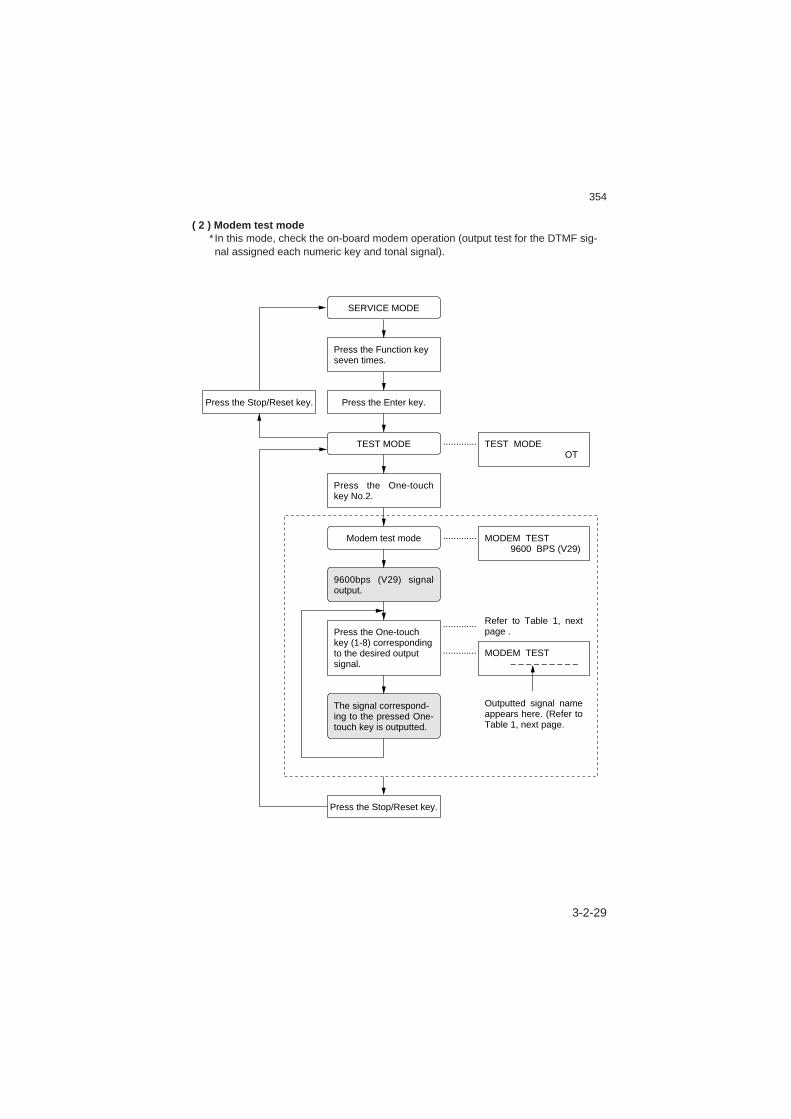
3-2-31
354
Press the One-touch key (1-8) corresponding to the desired output signal.
Press the Enter key.
Press the Stop/Reset key.
Press the Function keyseven times.
Press the One-touch key No.2.
9600bps (V29) signal output.
The signal correspond-ing to the pressed One-touch key is outputted.
Modem test mode
TEST MODE
SERVICE MODE
Press the Stop/Reset key.
TEST MODE OT
·············
MODEM TEST 9600 BPS (V29)
Outputted signal name appears here. (Refer to Table 1, next page.
·············
Refer to Table 1, next page .·············
············· MODEM TEST – – – – – – – – –
( 2 ) Modem test mode* In this mode, check the on-board modem operation (output test for the DTMF sig-nal assigned each numeric key and tonal signal).
3-2-29
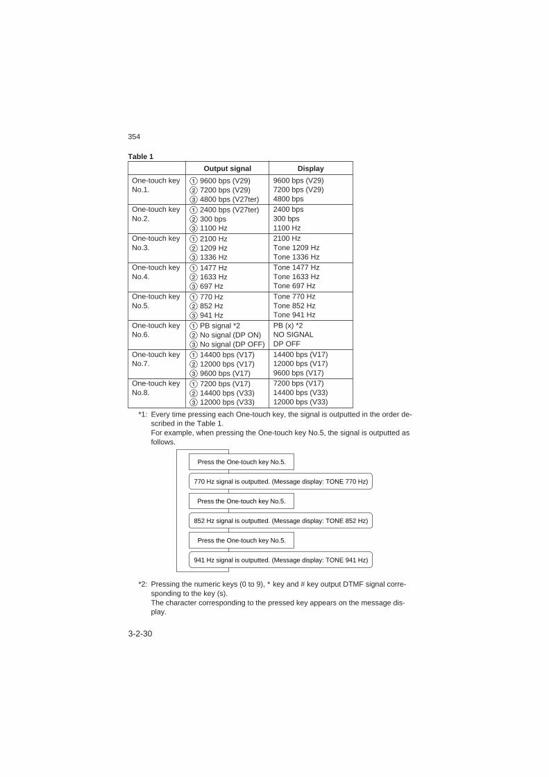
3-2-32
354
770 Hz signal is outputted. (Message display: TONE 770 Hz)
941 Hz signal is outputted. (Message display: TONE 941 Hz)
852 Hz signal is outputted. (Message display: TONE 852 Hz)
Press the One-touch key No.5.
Press the One-touch key No.5.
Press the One-touch key No.5.
*1: Every time pressing each One-touch key, the signal is outputted in the order de-scribed in the Table 1.For example, when pressing the One-touch key No.5, the signal is outputted asfollows.
*2: Pressing the numeric keys (0 to 9), ∗ key and # key output DTMF signal corre-sponding to the key (s).The character corresponding to the pressed key appears on the message dis-play.
One-touch keyNo.1.
One-touch keyNo.2.
One-touch keyNo.3.
One-touch keyNo.4.
One-touch keyNo.5.
One-touch keyNo.6.
One-touch keyNo.7.
One-touch keyNo.8.
1 9600 bps (V29)2 7200 bps (V29)3 4800 bps (V27ter)1 2400 bps (V27ter)2 300 bps3 1100 Hz1 2100 Hz2 1209 Hz3 1336 Hz1 1477 Hz2 1633 Hz3 697 Hz1 770 Hz2 852 Hz3 941 Hz1 PB signal *22 No signal (DP ON)3 No signal (DP OFF)1 14400 bps (V17)2 12000 bps (V17)3 9600 bps (V17)1 7200 bps (V17)2 14400 bps (V33)3 12000 bps (V33)
9600 bps (V29)7200 bps (V29)4800 bps2400 bps300 bps1100 Hz2100 HzTone 1209 HzTone 1336 HzTone 1477 HzTone 1633 HzTone 697 HzTone 770 HzTone 852 HzTone 941 HzPB (x) *2NO SIGNALDP OFF14400 bps (V17)12000 bps (V17)9600 bps (V17)7200 bps (V17)14400 bps (V33)12000 bps (V33)
Output signal Display
Table 1
3-2-30
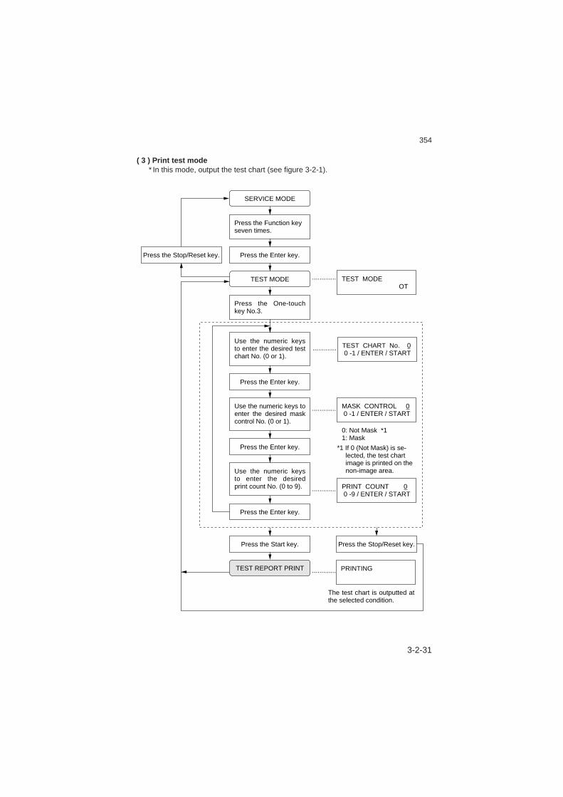
3-2-33
354
Use the numeric keys to enter the desired test chart No. (0 or 1).
Use the numeric keys to enter the desired print count No. (0 to 9).
Use the numeric keys to enter the desired mask control No. (0 or 1).
Press the Enter key.
Press the Enter key.
Press the Enter key.
Press the Enter key.
Press the Start key. Press the Stop/Reset key.
Press the Function keyseven times.
Press the One-touch key No.3.
TEST MODE
SERVICE MODE
Press the Stop/Reset key.
TEST CHART No. 0 0 -1 / ENTER / START
The test chart is outputted at the selected condition.
·············
TEST MODE OT
·············
MASK CONTROL 0 0 -1 / ENTER / START·············
PRINT COUNT 0 0 -9 / ENTER / START
PRINTING
·············
·············
0: Not Mask *11: Mask
*1 If 0 (Not Mask) is se-lected, the test chart image is printed on the non-image area.
TEST REPORT PRINT
( 3 ) Print test mode* In this mode, output the test chart (see figure 3-2-1).
3-2-31
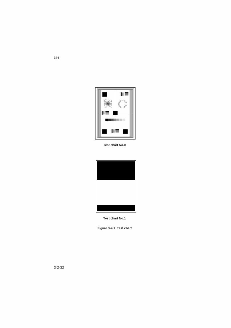
3-2-34
354
Test chart No.0
Test chart No.1
Figure 3-2-1 Test chart
3-2-32

3-2-35
354
( 4 ) Aging test mode* In this mode, check the printer section, document feed/image reading section(ADF) operation.
SERVICE MODE
Press the Enter key.
Press the Function keyseven times.
Press the One-touch key No.4.
TEST MODE
Press the Stop/Reset key.
TEST MODE OT
·············
CONT OPERATION ENTER / START
·······························
SCANNER ENTER / START
Press the Stop/Reset key.
Press the Enter key.
Press the Enter key.
Press the Start key.
SCANNER ON
SCANNER ON
·······························
A
B
*1
3-2-33
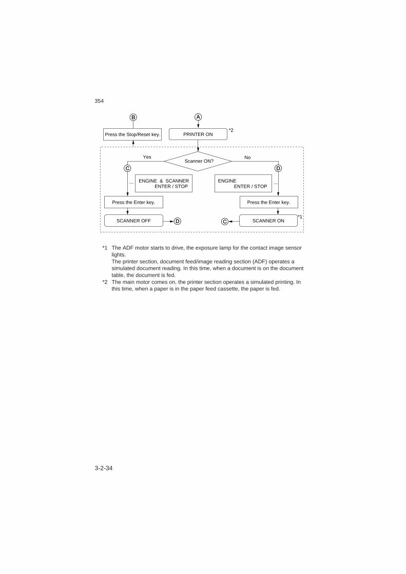
3-2-36
354
PRINTER ONPress the Stop/Reset key.
ENGINE ENTER / STOP
···
B A
*2
Scanner ON?
ENGINE & SCANNER ENTER / STOP
Press the Enter key.Press the Enter key.
SCANNER OFF SCANNER ON
···
C D
CD*1
Yes No
*1 The ADF motor starts to drive, the exposure lamp for the contact image sensorlights.The printer section, document feed/image reading section (ADF) operates asimulated document reading. In this time, when a document is on the documenttable, the document is fed.
*2 The main motor comes on, the printer section operates a simulated printing. Inthis time, when a paper is in the paper feed cassette, the paper is fed.
3-2-34
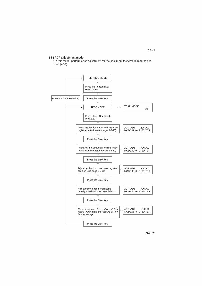
3-2-37
354
Press the Enter key.
Press the Function keyseven times.
Press the One-touch key No.5.
TEST MODE
SERVICE MODE
Press the Stop/Reset key.
TEST MODE OT
·······
Adjusting the document leading edge registration timing (see page 3-3-48).
Press the Enter key.
Adjusting the document trailing edge registration timing (see page 3-3-50).
Press the Enter key.
Adjusting the document reading start position (see page 3-3-52).
Press the Enter key.
Adjusting the document reading density threshold (see page 3-3-43).
Press the Enter key.
Do not change the setting of this mode other than the setting at the factory setting.
Press the Enter key.
··· ADF ADJ XXXXXMODE01 0 - 9 / ENTER
··· ADF ADJ XXXXXMODE02 0 - 9 / ENTER
··· ADF ADJ XXXXXMODE03 0 - 9 / ENTER
··· ADF ADJ XXXXXMODE04 0 - 9 / ENTER
·······ADF ADJ XXXXXMODE05 0 - 9 / ENTER
( 5 ) ADF adjustment mode* In this mode, perform each adjustment for the document feed/image reading sec-tion (ADF).
354-1
3-2-35

3-3-1
354
3-3-1 Precautions for assembly and disassembly
Precautions• Always unplug the power cord before starting disassembly and assembly operations.• Disconnect all connectors connected to this machine (computer connection cable,
telephone line, etc.) before starting these operations.• Remove the imaging unit, paper feed tray, document table, and eject tray before
starting these operations.• During disassembly, if wires are fastened with binding bands, you may cut these
bands as necessary, but if you cut them, always fasten those wires and return them totheir original positions during assembly.
• When handling PCBs, do not touch the PCB connection sections with your bare handsor damage them.
• When ICs are installed on a PCB, do not touch with bare hands or with any object thatmight carry a static electric charge.
• When replacing the fixing thermostat, always use the specified parts. Never use wireor the like instead of the specified thermostat. It can damage the machine and causeaccidents.
• Always use the tester indicated below when measuring voltage.
Hioki 3200Sanwa MD-180CSanwa YX-360TRBeckman TECH300Beckman 3030: Capable of measuring RMS values.Beckman 330: Capable of measuring RMS values.Beckman DM45Beckman DM850: Capable of measuring RMS values.Fluke 8060A: Capable of measuring RMS values.Arlec DMM1050Arlec YF1030C
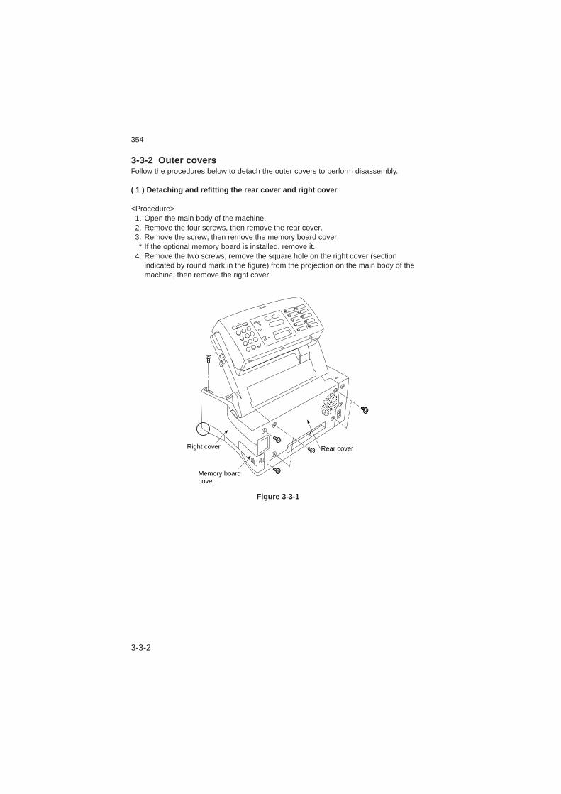
3-3-2
354
3-3-2 Outer coversFollow the procedures below to detach the outer covers to perform disassembly.
( 1 ) Detaching and refitting the rear cover and right cover
<Procedure> 1. Open the main body of the machine. 2. Remove the four screws, then remove the rear cover. 3. Remove the screw, then remove the memory board cover.
* If the optional memory board is installed, remove it. 4. Remove the two screws, remove the square hole on the right cover (section
indicated by round mark in the figure) from the projection on the main body of themachine, then remove the right cover.
Rear cover
Memory boardcover
Right cover
Figure 3-3-1

3-3-3
354
( 2 ) Detaching and refitting the left cover and left front cover
<Procedure> 1. Remove the rear cover. (See page 3-3-2.) 2. Remove the three screws, remove the three square holes on the left cover (sections
indicated by round marks in the figure) from the projections on the main body of themachine, then remove the left cover.
3. Remove the two screws, then remove the left front cover.
Left cover
Left frontcover
Figure 3-3-2
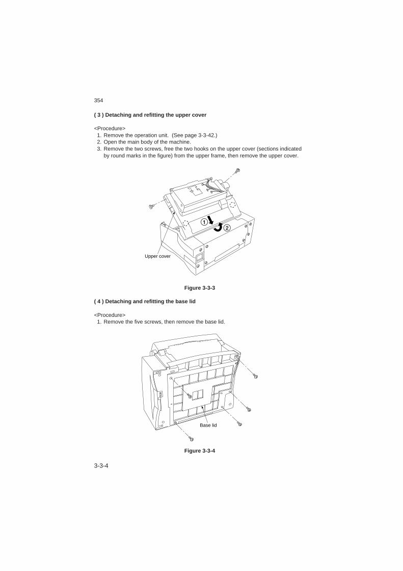
3-3-4
354
( 3 ) Detaching and refitting the upper cover
<Procedure> 1. Remove the operation unit. (See page 3-3-42.) 2. Open the main body of the machine. 3. Remove the two screws, free the two hooks on the upper cover (sections indicated
by round marks in the figure) from the upper frame, then remove the upper cover.
Upper cover
12
Figure 3-3-3
( 4 ) Detaching and refitting the base lid
<Procedure> 1. Remove the five screws, then remove the base lid.
Base lid
Figure 3-3-4
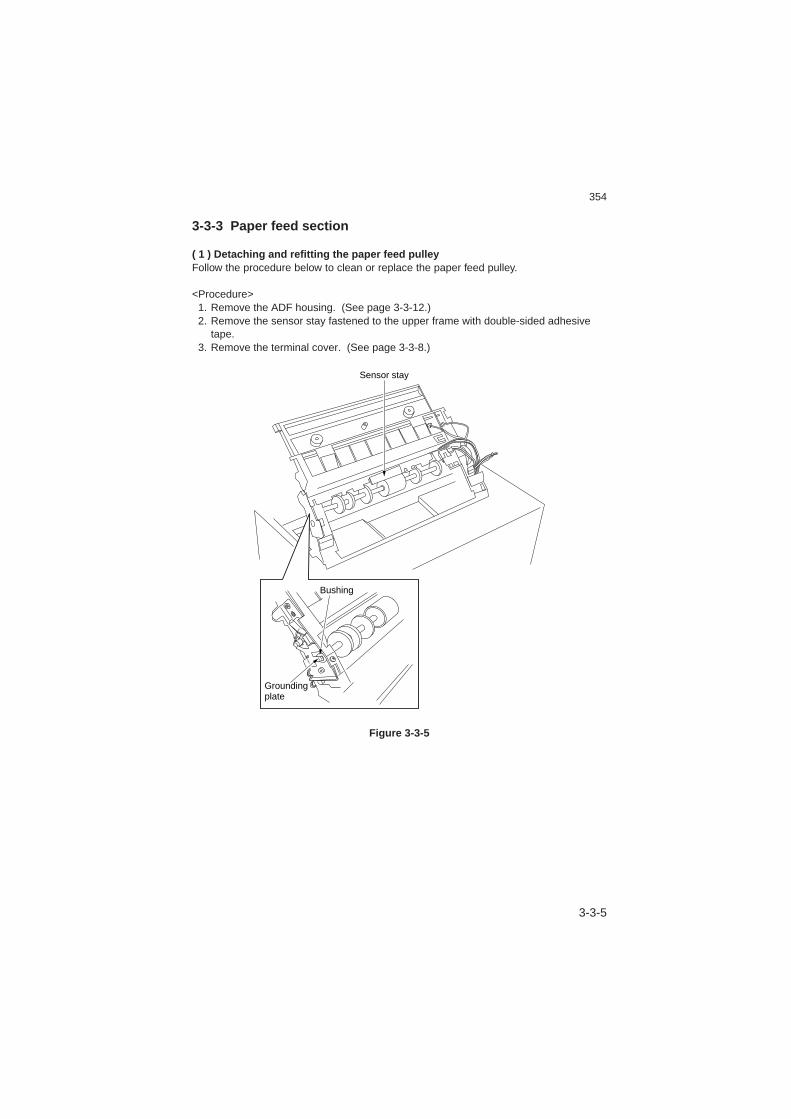
3-3-5
354
3-3-3 Paper feed section
( 1 ) Detaching and refitting the paper feed pulleyFollow the procedure below to clean or replace the paper feed pulley.
<Procedure> 1. Remove the ADF housing. (See page 3-3-12.) 2. Remove the sensor stay fastened to the upper frame with double-sided adhesive
tape. 3. Remove the terminal cover. (See page 3-3-8.)
Sensor stay
Bushing
Groundingplate
Figure 3-3-5
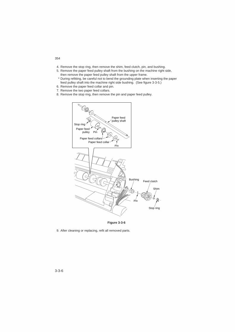
3-3-6
354
4. Remove the stop ring, then remove the shim, feed clutch, pin, and bushing. 5. Remove the paper feed pulley shaft from the bushing on the machine right side,
then remove the paper feed pulley shaft from the upper frame.* During refitting, be careful not to bend the grounding plate when inserting the paper
feed pulley shaft into the machine right side bushing. (See figure 3-3-5.) 6. Remove the paper feed collar and pin. 7. Remove the two paper feed collars. 8. Remove the stop ring, then remove the pin and paper feed pulley.
Bushing
Pin
Feed clutch
Shim
Stop ring
Pin
Paper feed collarsPaper feed collar
PinPaper feed
pulley
Stop ring
Paper feedpulley shaft
Figure 3-3-6
9. After cleaning or replacing, refit all removed parts.
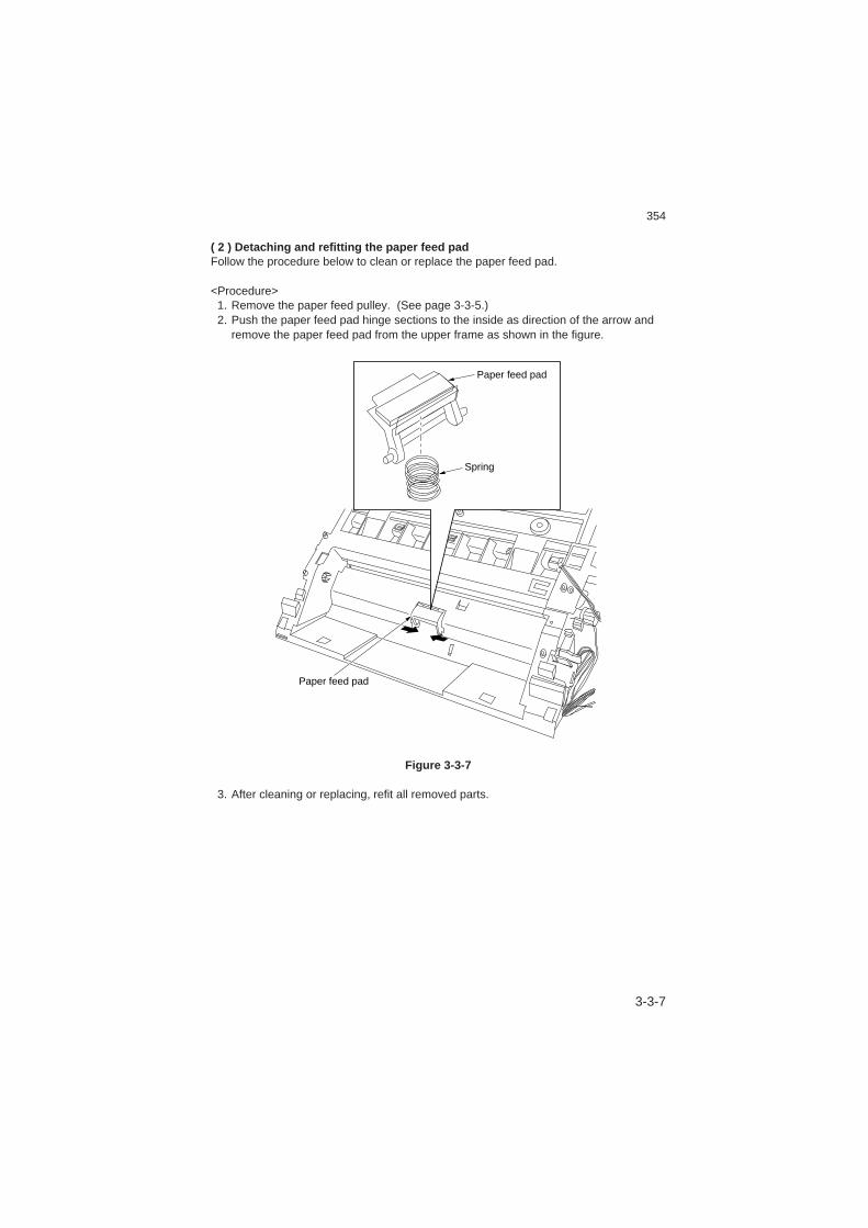
3-3-7
354
( 2 ) Detaching and refitting the paper feed padFollow the procedure below to clean or replace the paper feed pad.
<Procedure> 1. Remove the paper feed pulley. (See page 3-3-5.) 2. Push the paper feed pad hinge sections to the inside as direction of the arrow and
remove the paper feed pad from the upper frame as shown in the figure.
Paper feed pad
Spring
Paper feed pad
Figure 3-3-7
3. After cleaning or replacing, refit all removed parts.
3-3-8
354
( 3 ) Detaching and refitting the lower feed rollerFollow the procedure below to clean or replace the lower feed roller.
<Procedure> 1. Remove the screw, then remove the terminal cover.
* When refitting, the open/close strap hook section (section indicated by the roundmark in the figure) must be fastened by being securely installed on the projection ofthe terminal cover.
Terminal cover
Open/close strap
Figure 3-3-8

3-3-9
354
2. Remove the left and right crimp-style springs, then remove the lower feed roller.* When removing or refitting, be careful not to bend the grounding plate.
3. Remove the bushings and shims from both ends of the lower feed roller.
Shim
Lower feed roller
Bushing
Lower feed roller
Crimp-style spring
Grounding plate
Crimp-style spring
Figure 3-3-9
4. After cleaning or replacing, refit all removed parts.
3-3-10
354
( 4 ) Detaching and refitting the upper feed rollerFollow the procedure below to clean or replace the upper feed roller.
<Procedure> 1. Remove the lower feed roller. (See page 3-3-8.) 2. Remove the E ring, then remove the upper feed roller gear and bushing. 3. Remove the upper feed roller from the bushing on the right side of the machine. 4. Remove the bushing, then remove the upper feed roller.
* When removing or refitting, be careful not to bend the grounding plate.
Upper feed roller
Bushing
Grounding plate
Bushing
Upper feed roller gear
E ring
Figure 3-3-10
5. After cleaning or replacing, refit all removed parts.
3-3-11
354-1
3-3-4 Document feed and image reading sections (ADF)
( 1 ) Detaching and refitting the ADF guideFollow the procedure below to detach the ADF guide to perform disassembly.
<Procedure> 1. Remove the operation unit. (See page 3-3-42.) 2. Remove the screw, then remove the grounding wire from the ADF guide. 3. Disconnect the 3-pin connectors for the ADF timing switch and document detection
switch. 4. Remove the ferrite core installed on the wire. Pull out the grounding wire, the wires
for the two 3-pin connectors disconnected, and the wires for the connectorconnected to the operation unit from the hole on the ADF guide in the direction ofthe arrow.
5. Remove the retainer pin, remove the hinge for the ADF guide from the hole on theADF housing, then remove the ADF guide.
ADF guide
Grounding wire
Hinge
3-pin connectors
Retainer pin
Ferrite core
Figure 3-3-11
3-3-12
354
( 2 ) Detaching and refitting the ADF housingFollow the procedure below to detach the ADF housing to perform disassembly.
<Procedure> 1. Remove the ADF guide. (See page 3-3-11.) 2. Remove the contact image sensor (CIS). (See page 3-3-13.) 3. Remove the upper cover. (See page 3-3-4.) 4. Free the wires from the two cord clamp sections for the ADF housing. 5. Remove the screw, then remove the two grounding wires. 6. Remove the two screws, then remove the ADF housing as shown in the figure.
* When refitting, insert the two claws for the ADF housing into the bottom side of theupper frame and check that holes on the ADF housing are firmly placed into pins forthe upper frame. (sections indicated by round marks in the figure)
ADF housing
Grounding wires
Cord clampsections
Upper frame
ADF housing 21
Figure 3-3-12
3-3-13
354
( 3 ) Detaching and refitting the contact image sensor (CIS)Follow the procedure below to check or replace the contact image sensor.* During removing, if wires are fastened with binding bands, you may cut these bands
as necessary, but if you cut them, always fasten those wires and return them to theiroriginal positions during refitting.
<Procedure> 1. Remove the ADF guide. (See page 3-3-11.) 2. Insert flat-bladed screwdrivers or the like into three locations in the grooves on the
ADF guide, free the CIS retainer hooks, and pull the CIS retainer up and out, thenremove it from the ADF housing.
* When refitting, insert the two left and right claws for the CIS retainer securely intothe bottom side of the ADF housing (sections indicated with round marks in thefigure).
GroovesADF housing
CIS retainer
Contact imagesensor
Claw
Claw
CIS retainer Hooks
Hook
Figure 3-3-13
3-3-14
354
3. Gently remove the contact image sensor from the ADF housing. 4. Disconnect the connector, then remove the contact image sensor.
Contact image sensor
Connector
Figure 3-3-14
5. After checking or replacing, refit all removed parts.
3-3-15
354
( 4 ) Detaching and refitting the ADF padFollow the procedure below to clean or replace the ADF pad.
<Procedure> 1. Remove the ADF guide. (See page 3-3-11.) 2. Remove the two projections of the ADF guide from the square holes on the pad
plate spring, then remove the pad plate spring in the direction of the arrow. 3. Remove the ADF pad from the ADF guide.
ADF guide
Pad plate springADF pad
Projections
Squareholes
Pad plate spring
Figure 3-3-15
4. After cleaning or replacing, refit all removed parts.
3-3-16
354
( 5 ) Detaching and refitting the ADF paper feed roller and ADF conveying rollerFollow the procedure below to clean or replace the ADF paper feed roller and ADFconveying roller.
<Procedure> 1. Remove the ADF housing. (See Page 3-3-12.) 2. Remove the E ring, then remove the ADF conveying gear 36 from the ADF conveying
roller. 3. Remove the idle gear 16/37 from the drive pin for the ADF housing. 4. Remove the E ring, then remove the ADF paper feed gear 51 and ADF paper feed
square spring from the ADF paper feed roller. 5. Remove one E ring each and shift the bushings that fastens the ADF conveying
roller and ADF paper feed roller in the direction of the arrows, then remove the ADFconveying roller and ADF paper feed roller from the ADF housing.
* When refitting, be careful not to bend the grounding plate and check that eachbushing is firmly contacting the grounding terminal as shown in figure 3-3-17.
6. Remove the ADF paper feed roller and ADF conveying roller from the ADF housing. 7. Remove one bushing each from the ADF paper feed roller and ADF conveying roller.
Bushing
Bushing
ADF paper feed roller
ADF conveying roller
ADF housing
E ringE ring
E ring
Idle gear16/37
ADF paper feedsquare spring
ADF paper feed gear 51
ADF conveyinggear 36
E ring
Figure 3-3-16
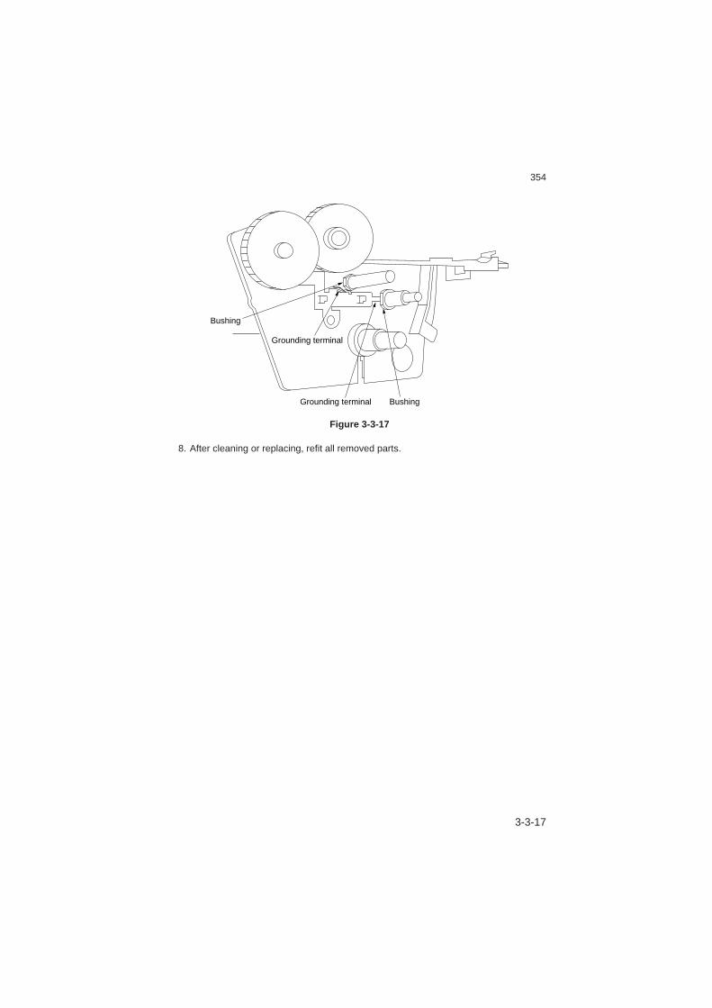
3-3-17
354
Bushing
Bushing
Grounding terminal
Grounding terminal
Figure 3-3-17
8. After cleaning or replacing, refit all removed parts.

3-3-18
354
( 6 ) Detaching and refitting the ADF eject rollerFollow the procedure below to clean or replace the ADF eject roller.
<Procedure> 1. Remove the ADF housing. (See page 3-3-12.) 2. Remove the E ring, then remove the ADF conveying gear 36 from the ADF eject
roller. 3. Remove the E ring, shift the bushing that fastens the ADF eject roller in the direction
of the arrow, then remove ADF eject roller from the ADF housing.* When refitting, be careful not to bend the grounding plate and check that the
bushing is firmly contacting the grounding terminal as shown in figure 3-3-19. 4. Remove the ADF eject roller from the ADF housing. 5. Remove the bushing from the ADF eject roller.
ADF eject roller
Bushing
E ring
E ring
ADF conveying gear 36
Figure 3-3-18
Bushing
Groundingterminal
Figure 3-3-19
6. After cleaning or replacing, refit all removed parts.
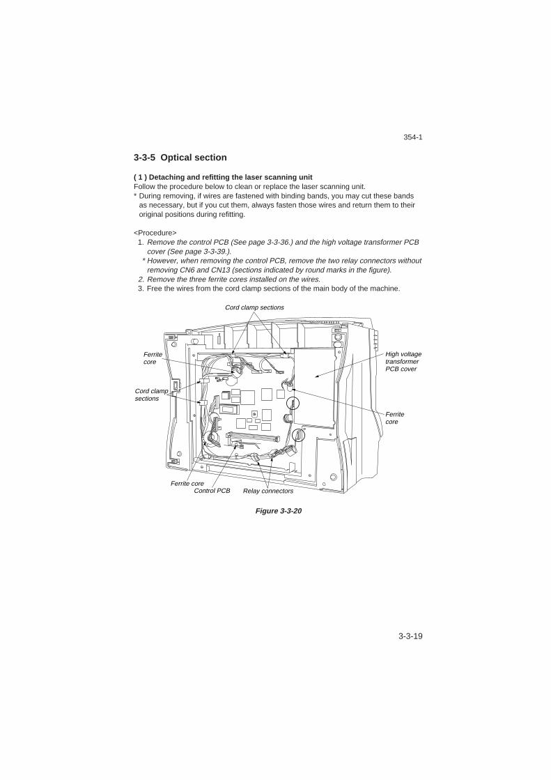
3-3-19
354-1
3-3-5 Optical section
( 1 ) Detaching and refitting the laser scanning unitFollow the procedure below to clean or replace the laser scanning unit.* During removing, if wires are fastened with binding bands, you may cut these bands
as necessary, but if you cut them, always fasten those wires and return them to theiroriginal positions during refitting.
<Procedure> 1. Remove the control PCB (See page 3-3-36.) and the high voltage transformer PCB
cover (See page 3-3-39.).* However, when removing the control PCB, remove the two relay connectors without
removing CN6 and CN13 (sections indicated by round marks in the figure). 2. Remove the three ferrite cores installed on the wires. 3. Free the wires from the cord clamp sections of the main body of the machine.
Cord clamp sections
Cord clamp sections
Relay connectors
High voltagetransformerPCB cover
Ferritecore
Ferritecore
Ferrite coreControl PCB
Figure 3-3-20

3-3-20
354
4. Remove the power source PCB. (See page 3-3-40.) 5. Remove the two screws, then remove the cooling fan. 6. Remove the two screws, then remove the three grounding wires from the chassis. 7. Pull out the connector wires connected to the control PCB from the square hole in
the cooling fan rear side chassis.
Screw
Screw
Grounding wires Grounding wire
Cooling fanSquare hole
Chassis
Figure 3-3-21
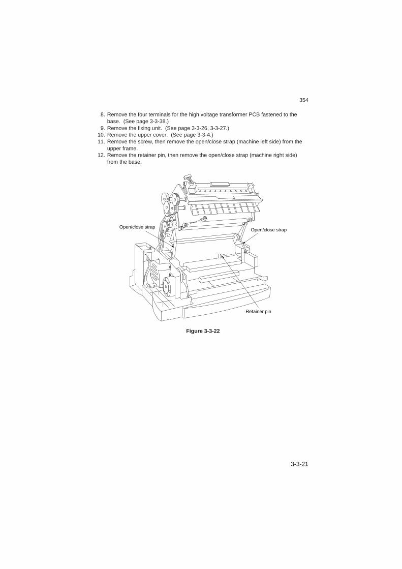
3-3-21
354
8. Remove the four terminals for the high voltage transformer PCB fastened to thebase. (See page 3-3-38.)
9. Remove the fixing unit. (See page 3-3-26, 3-3-27.)10. Remove the upper cover. (See page 3-3-4.)11. Remove the screw, then remove the open/close strap (machine left side) from the
upper frame.12. Remove the retainer pin, then remove the open/close strap (machine right side)
from the base.
Retainer pin
Open/close strapOpen/close strap
Figure 3-3-22
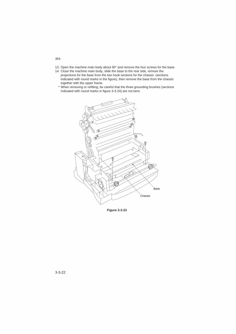
3-3-22
354
13. Open the machine main body about 90° and remove the four screws for the base.14. Close the machine main body, slide the base to the rear side, remove the
projections for the base from the two hook sections for the chassis (sectionsindicated with round marks in the figure), then remove the base from the chassistogether with the upper frame.
* When removing or refitting, be careful that the three grounding brushes (sectionsindicated with round marks in figure 3-3-24) are not bent.
Chassis
Base
Figure 3-3-23
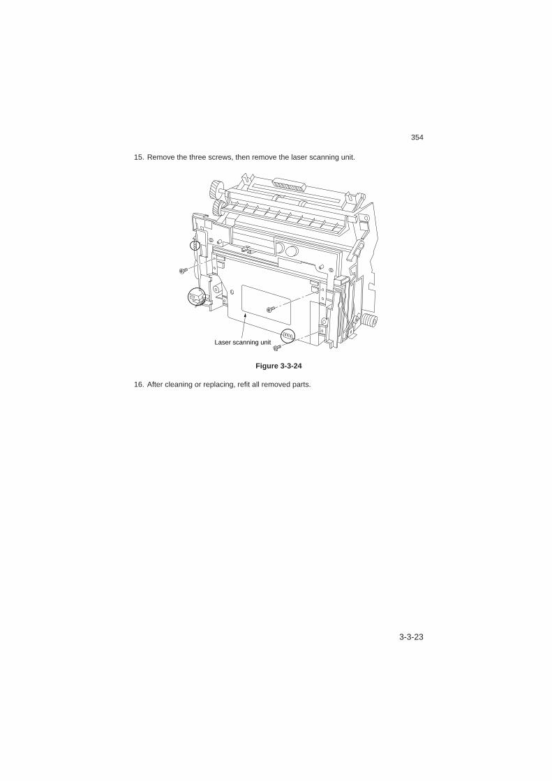
3-3-23
354
15. Remove the three screws, then remove the laser scanning unit.
Laser scanning unit
Figure 3-3-24
16. After cleaning or replacing, refit all removed parts.
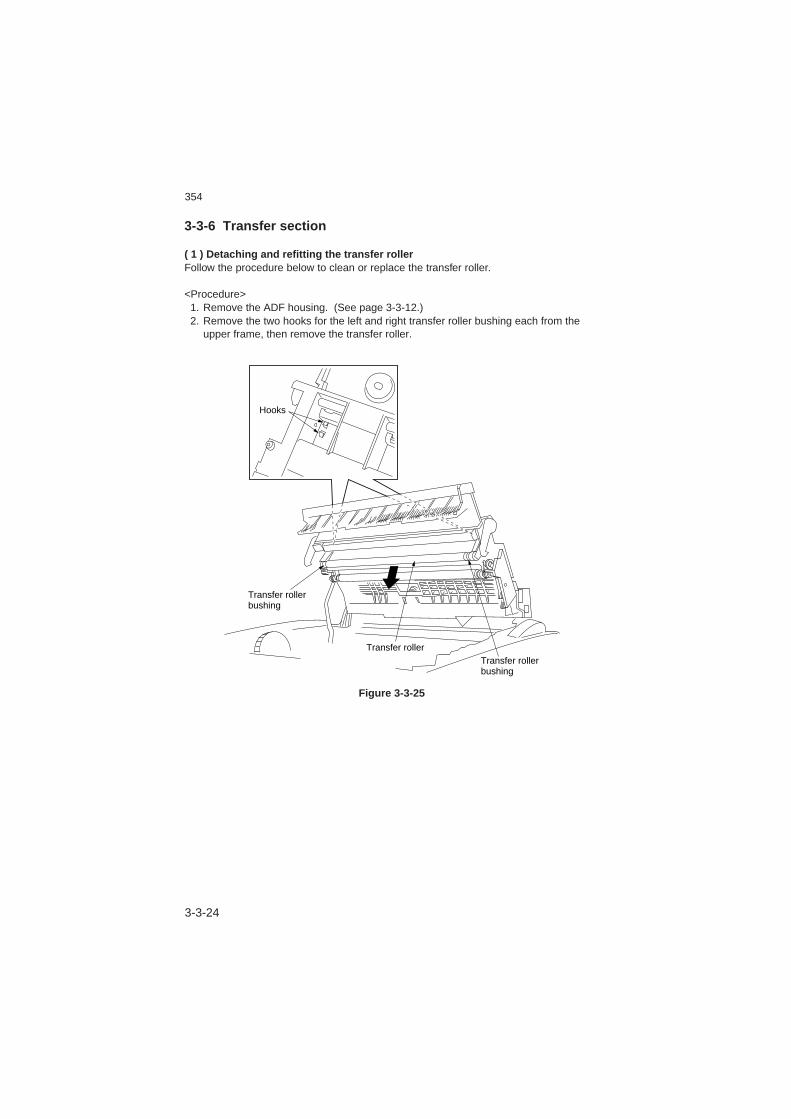
3-3-24
354
3-3-6 Transfer section
( 1 ) Detaching and refitting the transfer rollerFollow the procedure below to clean or replace the transfer roller.
<Procedure> 1. Remove the ADF housing. (See page 3-3-12.) 2. Remove the two hooks for the left and right transfer roller bushing each from the
upper frame, then remove the transfer roller.
Hooks
Transfer rollerbushing
Transfer rollerbushing
Transfer roller
Figure 3-3-25

3-3-25
354
3. Remove the transfer roller pulleys, transfer roller bushings, and transfer springsfrom the transfer roller as shown in the figure.
Transfer roller pulley
Transfer roller pulley
Transfer spring
Transfer spring
Transfer roller
Transfer roller bushing
Transfer roller bushing
Figure 3-3-26
4. After cleaning or replacing, refit all removed parts.
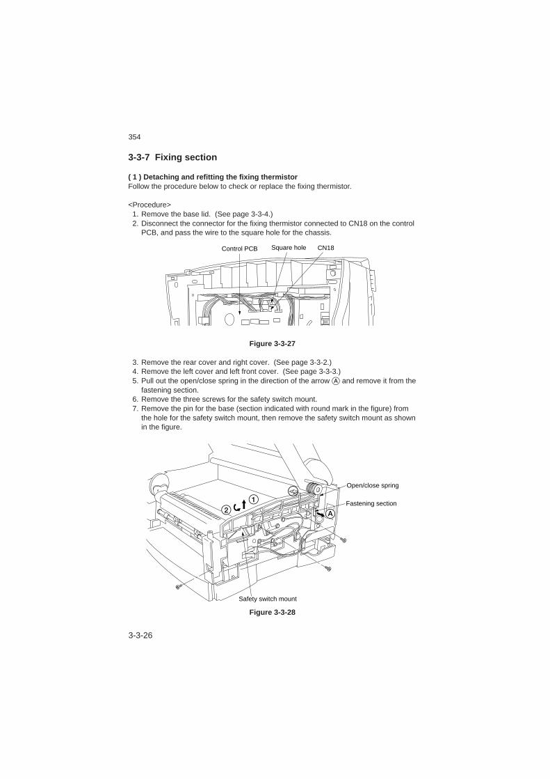
3-3-26
354
Control PCB Square hole CN18
3-3-7 Fixing section
( 1 ) Detaching and refitting the fixing thermistorFollow the procedure below to check or replace the fixing thermistor.
<Procedure> 1. Remove the base lid. (See page 3-3-4.) 2. Disconnect the connector for the fixing thermistor connected to CN18 on the control
PCB, and pass the wire to the square hole for the chassis.
Figure 3-3-27
3. Remove the rear cover and right cover. (See page 3-3-2.) 4. Remove the left cover and left front cover. (See page 3-3-3.) 5. Pull out the open/close spring in the direction of the arrow A and remove it from the
fastening section. 6. Remove the three screws for the safety switch mount. 7. Remove the pin for the base (section indicated with round mark in the figure) from
the hole for the safety switch mount, then remove the safety switch mount as shownin the figure.
Open/close spring
Fastening section
Safety switch mount
1
A2
Figure 3-3-28
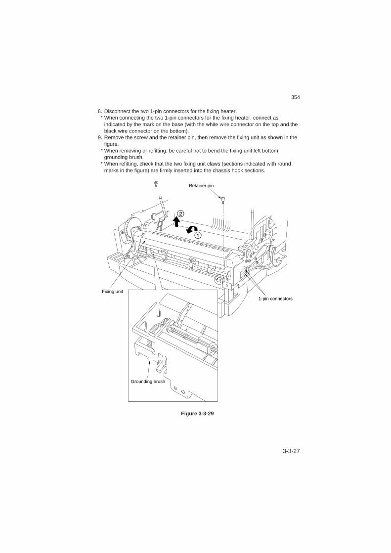
3-3-27
354
8. Disconnect the two 1-pin connectors for the fixing heater.* When connecting the two 1-pin connectors for the fixing heater, connect as
indicated by the mark on the base (with the white wire connector on the top and theblack wire connector on the bottom).
9. Remove the screw and the retainer pin, then remove the fixing unit as shown in thefigure.
* When removing or refitting, be careful not to bend the fixing unit left bottomgrounding brush.
* When refitting, check that the two fixing unit claws (sections indicated with roundmarks in the figure) are firmly inserted into the chassis hook sections.
2
1
Fixing unit
Retainer pin
1-pin connectors
Grounding brush
Figure 3-3-29
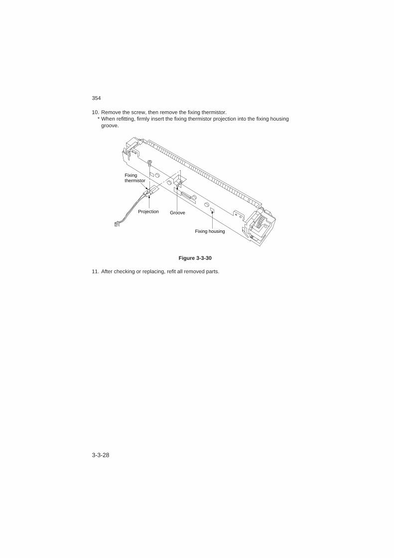
3-3-28
354
10. Remove the screw, then remove the fixing thermistor.* When refitting, firmly insert the fixing thermistor projection into the fixing housing
groove.
Fixing housing
Fixingthermistor
Projection Groove
Figure 3-3-30
11. After checking or replacing, refit all removed parts.
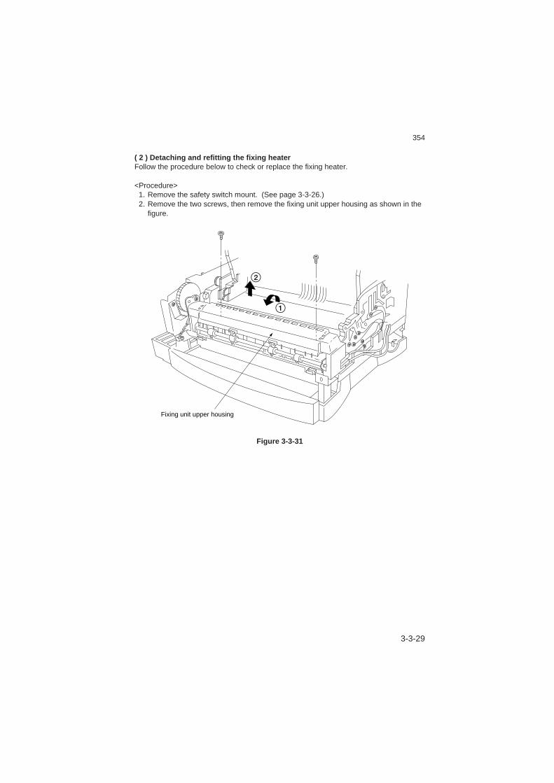
3-3-29
354
( 2 ) Detaching and refitting the fixing heaterFollow the procedure below to check or replace the fixing heater.
<Procedure> 1. Remove the safety switch mount. (See page 3-3-26.) 2. Remove the two screws, then remove the fixing unit upper housing as shown in the
figure.
2
1
Fixing unit upper housing
Figure 3-3-31
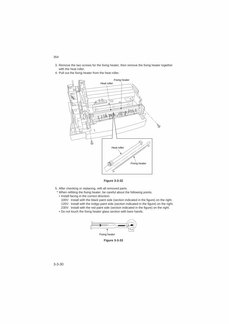
3-3-30
354
3. Remove the two screws for the fixing heater, then remove the fixing heater togetherwith the heat roller.
4. Pull out the fixing heater from the heat roller.
Heat roller
Heat roller
Fixing heater
Fixing heater
Figure 3-3-32
5. After checking or replacing, refit all removed parts.* When refitting the fixing heater, be careful about the following points.
• Install facing in the correct direction.100V: Install with the black paint side (section indicated in the figure) on the right.120V: Install with the indigo paint side (section indicated in the figure) on the right.230V: Install with the red paint side (section indicated in the figure) on the right.
• Do not touch the fixing heater glass section with bare hands.
Fixing heater
Figure 3-3-33
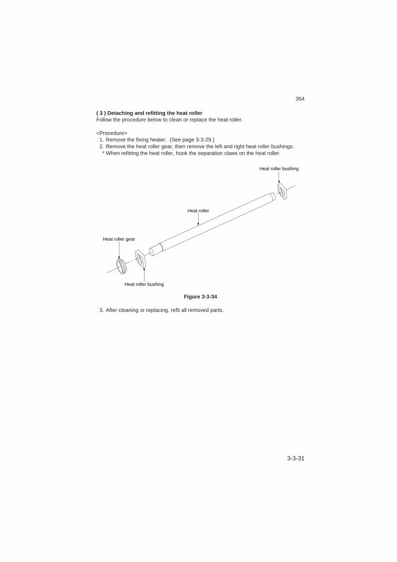
3-3-31
354
( 3 ) Detaching and refitting the heat rollerFollow the procedure below to clean or replace the heat roller.
<Procedure> 1. Remove the fixing heater. (See page 3-3-29.) 2. Remove the heat roller gear, then remove the left and right heat roller bushings.
* When refitting the heat roller, hook the separation claws on the heat roller.
Heat roller gear
Heat roller bushing
Heat roller
Heat roller bushing
Figure 3-3-34
3. After cleaning or replacing, refit all removed parts.

3-3-32
354
( 4 ) Detaching and refitting the press rollerFollow the procedure below to clean or replace the press roller.
<Procedure> 1. Remove the fixing unit upper housing. (See page 3-3-29.) 2. Open the fixing unit upper housing left and right press roller bushing hook sections
(sections indicated by round marks in the figure) to the outside and remove thepress roller together with the press roller bushing.
3. Remove the press roller bushings and press springs from the press roller.
Press roller
Press roller
Press roller bushing
Pressspring
Figure 3-3-35
4. After cleaning or replacing, refit all removed parts.

3-3-33
354
( 5 ) Detaching and refitting the separation clawFollow the procedure below to clean or replace the separation claw.
<Procedure> 1. Remove the heat roller. (See page 3-3-31.) 2. Remove the one spring each, then remove the two separation claws.
* When the separation claws are installed, they must hook on the heat roller.
Separation claw
Spring
Figure 3-3-36
3. After cleaning or replacing, refit all removed parts.
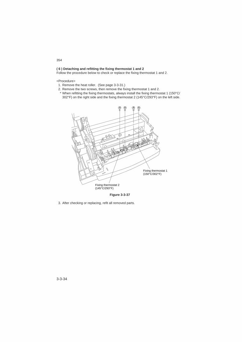
3-3-34
354
( 6 ) Detaching and refitting the fixing thermostat 1 and 2Follow the procedure below to check or replace the fixing thermostat 1 and 2.
<Procedure> 1. Remove the heat roller. (See page 3-3-31.) 2. Remove the two screws, then remove the fixing thermostat 1 and 2.
* When refitting the fixing thermostats, always install the fixing thermostat 1 (150°C/302°F) on the right side and the fixing thermostat 2 (145°C/293°F) on the left side.
Fixing thermostat 2 (145°C/293°F)
Fixing thermostat 1 (150°C/302°F)
Figure 3-3-37
3. After checking or replacing, refit all removed parts.

3-3-35
354-1
( 7 ) Detaching and refitting the eject rollerFollow the procedure below to clean or replace the eject roller.
<Procedure> 1. Remove the fixing unit upper housing. (See page 3-3-29.) 2. Remove the stop ring, then remove the fixing idle gear. 3. Slide the eject roller in the direction of the arrow and remove it from the fixing unit.
Eject roller
Eject roller
Fixing idle gear
Stop ring
Figure 3-3-38
4. After cleaning or replacing, refit all removed parts.
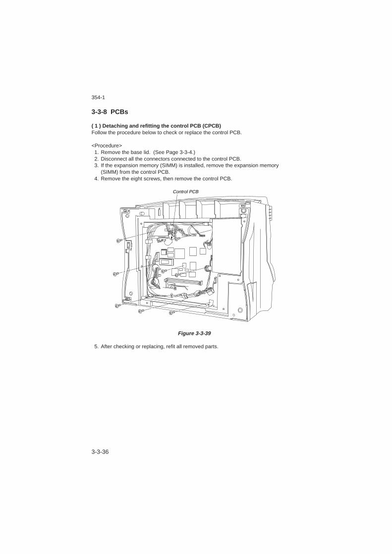
3-3-36
354-1
3-3-8 PCBs
( 1 ) Detaching and refitting the control PCB (CPCB)Follow the procedure below to check or replace the control PCB.
<Procedure> 1. Remove the base lid. (See Page 3-3-4.) 2. Disconnect all the connectors connected to the control PCB. 3. If the expansion memory (SIMM) is installed, remove the expansion memory
(SIMM) from the control PCB. 4. Remove the eight screws, then remove the control PCB.
Control PCB
Figure 3-3-39
5. After checking or replacing, refit all removed parts.
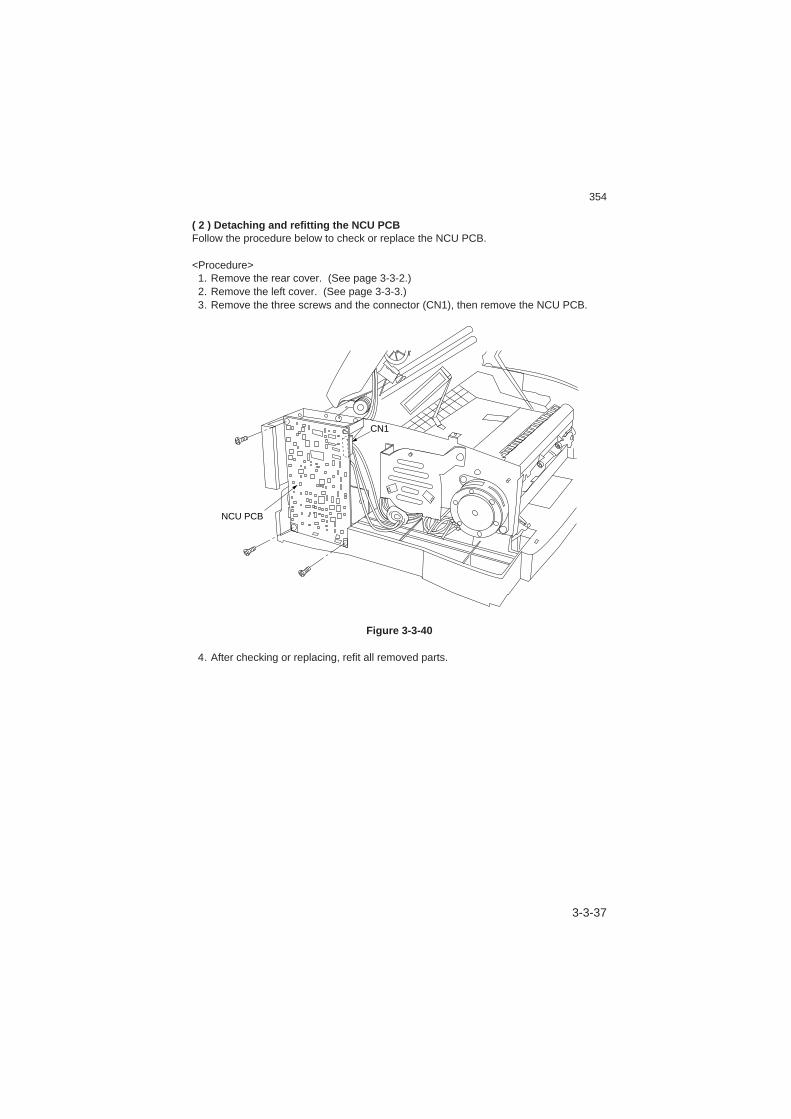
3-3-37
354
( 2 ) Detaching and refitting the NCU PCBFollow the procedure below to check or replace the NCU PCB.
<Procedure> 1. Remove the rear cover. (See page 3-3-2.) 2. Remove the left cover. (See page 3-3-3.) 3. Remove the three screws and the connector (CN1), then remove the NCU PCB.
CN1
NCU PCB
Figure 3-3-40
4. After checking or replacing, refit all removed parts.
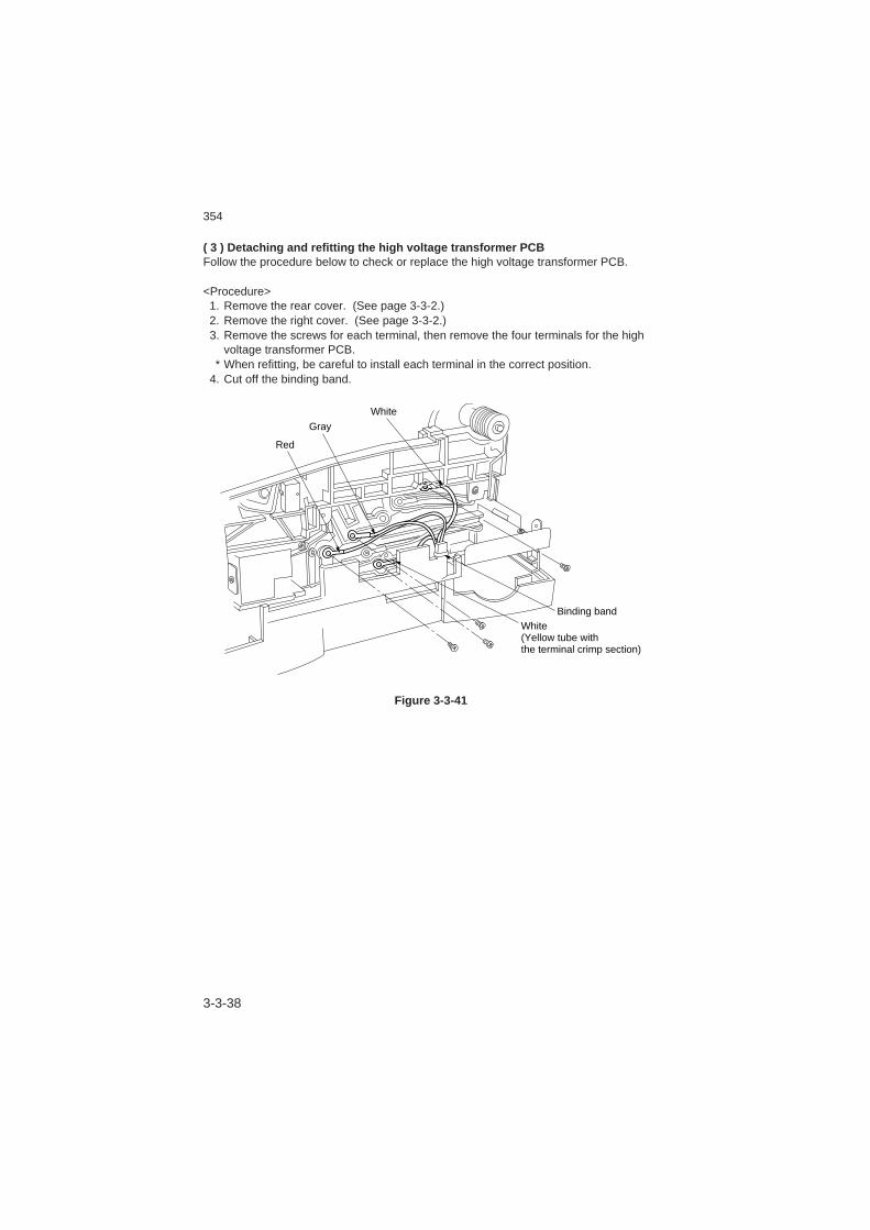
3-3-38
354
( 3 ) Detaching and refitting the high voltage transformer PCBFollow the procedure below to check or replace the high voltage transformer PCB.
<Procedure> 1. Remove the rear cover. (See page 3-3-2.) 2. Remove the right cover. (See page 3-3-2.) 3. Remove the screws for each terminal, then remove the four terminals for the high
voltage transformer PCB.* When refitting, be careful to install each terminal in the correct position.
4. Cut off the binding band.
White(Yellow tube with the terminal crimp section)
Binding band
Red
Gray
White
Figure 3-3-41
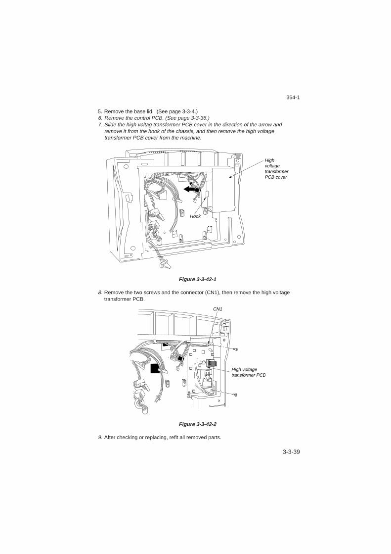
3-3-39
354-1
5. Remove the base lid. (See page 3-3-4.) 6. Remove the control PCB. (See page 3-3-36.) 7. Slide the high voltag transformer PCB cover in the direction of the arrow and
remove it from the hook of the chassis, and then remove the high voltagetransformer PCB cover from the machine.
High voltagetransformerPCB cover
Hook
Figure 3-3-42-1
8. Remove the two screws and the connector (CN1), then remove the high voltagetransformer PCB.
CN1
High voltagetransformer PCB
Figure 3-3-42-2
9. After checking or replacing, refit all removed parts.

3-3-40
354
( 4 ) Detaching and refitting the power source PCBFollow the procedure below to check or replace the power source PCB.* During removing, if wires are fastened with binding bands, you may cut these bands
as necessary, but if you cut them, always fasten those wires and return them to theiroriginal positions during refitting.
<Procedure> 1. Remove the rear cover and right cover. (See page 3-3-2.) 2. Remove the left cover. (See page 3-3-3.) 3. Remove the eight screws, then remove the rear cover mount.
Rear cover mount
Figure 3-3-43
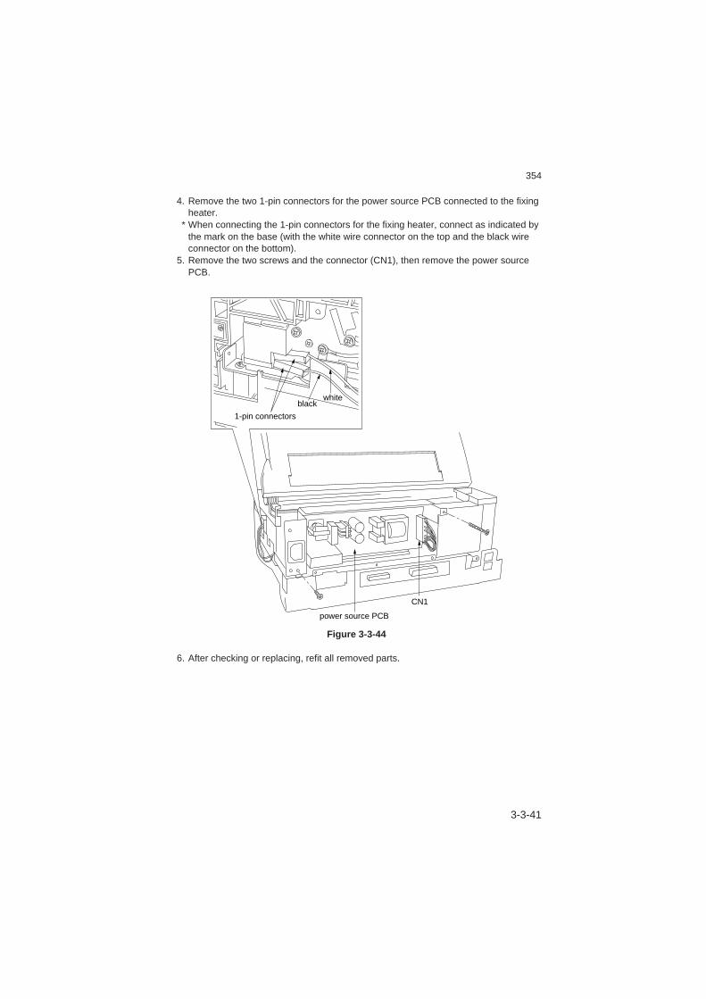
3-3-41
354
4. Remove the two 1-pin connectors for the power source PCB connected to the fixingheater.
* When connecting the 1-pin connectors for the fixing heater, connect as indicated bythe mark on the base (with the white wire connector on the top and the black wireconnector on the bottom).
5. Remove the two screws and the connector (CN1), then remove the power sourcePCB.
power source PCB
CN1
1-pin connectors
blackwhite
Figure 3-3-44
6. After checking or replacing, refit all removed parts.
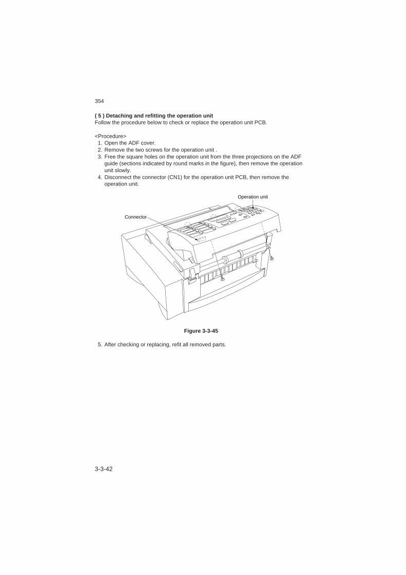
3-3-42
354
( 5 ) Detaching and refitting the operation unitFollow the procedure below to check or replace the operation unit PCB.
<Procedure> 1. Open the ADF cover. 2. Remove the two screws for the operation unit . 3. Free the square holes on the operation unit from the three projections on the ADF
guide (sections indicated by round marks in the figure), then remove the operationunit slowly.
4. Disconnect the connector (CN1) for the operation unit PCB, then remove theoperation unit.
Operation unit
Connector
Figure 3-3-45
5. After checking or replacing, refit all removed parts.
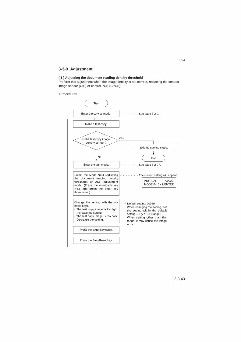
3-3-43
354
3-3-9 Adjustment
( 1 ) Adjusting the document reading density thresholdPreform this adjustment when the image density is not correct, replacing the contactimage sensor (CIS) or control PCB (CPCB).
<Procedure>
Is the test copy imagedensity correct ?
No
Yes
Select the Mode No.4 (Adjusting the document reading density threshold) of ADF adjustment mode. (Press the one-touch key No.5 and press the enter key three times.)
Change the setting with the nu-meric keys.• The test copy image is too light:
Increase the setting.• The test copy image is too dark:
Decrease the setting.
Enter the test mode.
Exit the service mode.
Make a test copy.
Enter the service mode.
Press the Stop/Reset key.
Press the Enter key twice.
Start
End
· · · · · · · · · · · · See page 3-2-2.
· · · · · · · · · · · · See page 3-2-27.
· · · · · · · · · · · · The current setting will appear.
* Default setting: 00029When changing the setting, set the setting within the default setting ± 2 (27 - 31) range .When setting other than this range, it may cause the image error.
ADF ADJ 00029MODE 04 0 - 9/ENTER
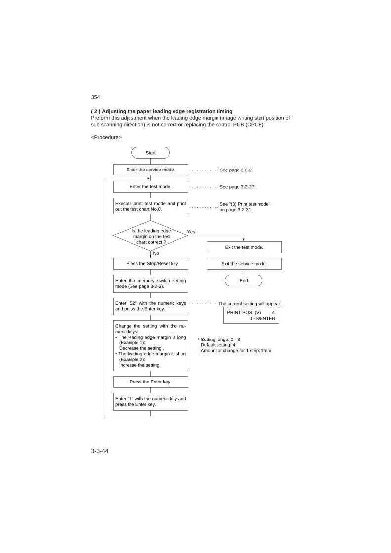
3-3-44
354
( 2 ) Adjusting the paper leading edge registration timingPreform this adjustment when the leading edge margin (image writing start position ofsub scanning direction) is not correct or replacing the control PCB (CPCB).
<Procedure>
Is the leading edge margin on the test
chart correct ?
No
Yes
Enter the memory switch setting mode (See page 3-2-3).
Enter "1" with the numeric key and press the Enter key.
Enter "52" with the numeric keys and press the Enter key.
Change the setting with the nu-meric keys.• The leading edge margin is long
(Example 1):Decrease the setting .
• The leading edge margin is short (Example 2):Increase the setting.
Press the Stop/Reset key
Exit the test mode.
Exit the service mode.
Enter the test mode.
Execute print test mode and print out the test chart No.0.
Enter the service mode.
Press the Enter key.
Start
End
· · · · · · · · · · · · See page 3-2-2.
· · · · · · · · · · · · See page 3-2-27.
· · · · · · · · · · · ·See "(3) Print test mode"on page 3-2-31.
· · · · · · · · · · · ·The current setting will appear.
* Setting range: 0 - 8Default setting: 4Amount of change for 1 step: 1mm
PRINT POS. (V) 40 - 8/ENTER

3-3-45
354
Example 1 Example 2
Standard setting of leading edge margin: 3 mm ± 2.5 mm
Figure 3-3-46

3-3-46
354
( 3 ) Adjusting the center registrationPerform this adjustment when there is not align between the center of the printing imageand the center of the document image (The printing image is shifted toward the right orthe left side: image writing start position of main scanning direction is not correct) orreplacing the control PCB (CPCB).
<Procedure>
Is the printing image shifted toward the right or
left side ?
No
Yes
Enter the memory switch setting mode (See page 3-2-3).
Enter "53" with the numeric keys and press the Enter key.
Change the setting with the nu-meric keys.• The printing image is shifted to-
ward the right side (Example 1):Decrease the setting .
• The printing image is shifted to-ward the left side (Example 2):Increase the setting.
Press the Stop/Reset key.
Exit the test mode.
Exit the service mode.
Enter the test mode.
Execute print test mode and print out the test chart No.0.
Enter the service mode.
Enter "1" with the numeric key and press the Enter key.
Press the Enter key.
Start
End
· · · · · · · · · · · · See page 3-2-2.
· · · · · · · · · · · · See page 3-2-27.
· · · · · · · · · · · ·See "(3) Print test mode"on page 3-2-31.
· · · · · · · · · · · ·The current setting will appear.
* Setting range: 0 - 8Default setting: 4Amount of change for 1 step: 1 mm
PRINT POS. (H) 40 - 8/ENTER
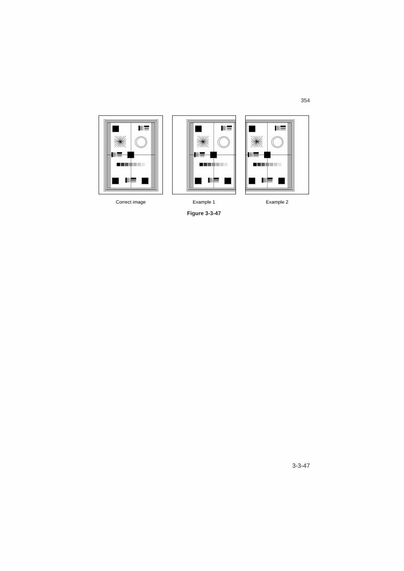
3-3-47
354
Correct image Example 1 Example 2
Figure 3-3-47
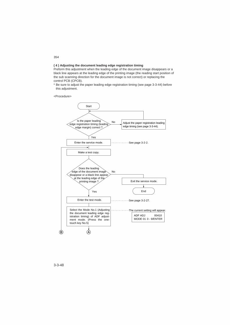
3-3-48
354
( 4 ) Adjusting the document leading edge registration timingPreform this adjustment when the leading edge of the document image disappears or ablack line appears at the leading edge of the printing image (the reading start position ofthe sub scanning direction for the document image is not correct) or replacing thecontrol PCB (CPCB).* Be sure to adjust the paper leading edge registration timing (see page 3-3-44) before
this adjustment.
<Procedure>
Enter the service mode.
Start
AB
Make a test copy.
No
No
Yes
Enter the test mode.
Select the Mode No.1 (Adjusting the document leading edge reg-istration timing) of ADF adjust-ment mode. (Press the one-touch key No.5)
Exit the service mode.
End
· · · · · · · · · · · ·See page 3-2-27.
· · · · · · · · · · · ·See page 3-2-2.
Is the paper leading edge registration timing (leading
edge margin) correct ?
Does the leadingedge of the document image
disappear or a black line appear at the leading edge of the
printing image ?
Yes
Adjust the paper registration leading edge timing (see page 3-3-44).
· · · · · · · · · · · ·The current setting will appear.
ADF ADJ 00410MODE 01 0 - 9/ENTER
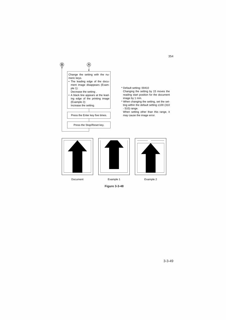
3-3-49
354
Figure 3-3-48
Press the Enter key five times.
Change the setting with the nu-meric keys.• The leading edge of the docu-
ment image disappears (Exam-ple 1):Decrease the setting .
• A black line appears at the lead-ing edge of the printing image (Example 2):Increase the setting.
Press the Stop/Reset key.
AB
* Default setting: 00410Changing the setting by 15 moves the reading start position for the document image by 1 mm.
* When changing the setting, set the set-ting within the default setting ±100 (310 - 510) range.When setting other than this range, it may cause the image error.
Document Example 2Example 1
3-3-50
354
( 5 ) Adjusting the document trailing edge registration timingPreform this adjustment when the trailing edge of the document image disappears or ablack line appears at the trailing edge of the printing image (the reading end position ofthe sub scanning direction for the document image is not correct) or replacing thecontrol PCB (CPCB).
<Procedure>
Enter the service mode.
Start
AB
Make a test copy.
No
Yes
Enter the test mode.
Select the Mode No.2 (Adjusting document trailing edge registra-tion timing) of ADF adjustment mode. (Press the one-touch key No.5 and press the Enter key)
Exit the service mode.
End
· · · · · · · · · · · ·See page 3-2-27.
· · · · · · · · · · · ·See page 3-2-2.
Does the trailing edge of the document
image disappear or a black line appear at the trailing edge
of the printing image ?
· · · · · · · · · · · ·The current setting will appear.
ADF ADJ 00280MODE 02 0 - 9/ENTER
3-3-51
354
Figure 3-3-49
Press the Enter key four times.
Change the setting with the nu-meric keys.• The trailing edge of the docu-
ment image disappears (Exam-ple 1):Increase the setting.
• A black line appears at the trail-ing edge of the printing image (Example 2):Decrease the setting .
Press the Stop/Reset key.
AB
* Default setting: 00280Changing the setting by 25 moves the reading end position for the document image by 1 mm.
* When changing the setting, set the set-ting within the default setting ±150 (130 - 430) range.When setting other than this range, it may cause the image error.
Document Example 2Example 1

3-3-52
354
( 6 ) Adjusting the document reading start position (main scanning direction)Preform this adjustment when a black line appears at the left side of the printing image(the start position of the main scanning direction for the document image is not correct)or replacing the control PCB (CPCB).* Be sure to adjust the center registration (see page 3-3-46) before this adjustment.
<Procedure>
Enter the service mode.
Start
AB
Make a test copy.
No
No
Yes
Enter the test mode.
Select the Mode No.3 (Adjusting document reading start position) of ADF adjustment mode. (Press the one-touch key No.5 and press the Enter key twice)
Exit the service mode.
End
· · · · · · · · · · · ·See page 3-2-27.
· · · · · · · · · · · ·See page 3-2-2.
Is the center registration correct ?
Does a black line appear at the left side of
the printing image ? (Example 1)
Yes
Adjust the center registration (see page 3-3-46).
· · · · · · · · · · · ·The current setting will appear.
ADF ADJ 00002MODE 03 0 - 9/ENTER
3-3-53
354
Figure 3-3-50
Press the Enter key three times.
Increase the setting with the nu-meric keys.
Press the Stop/Reset key.
AB
* Default setting: 00002Changing the setting by 10 moves the start position for the document image by 1 mm.
* When changing the setting, set the set-ting within 2 - 50 range.When setting other than this range, it may cause the image error.
Document Example 1
354
3-4-1
3-4-1 Replacing the control PCBWhen replacing the control PCB, perform the following procedures.
<Procedure>• Before replacing
Perform the following procedures, verify the settings of the user setting items, memoryswitch setting items and test mode adjustment settings which must be reentered afterreplacement.
1. Print out the dial list. 2. Enter the service mode. 3. Print out the preset list. * Print out the preset list with the same procedure as the user mode. 4. Enter the test mode. 5. Execute the ADF adjustment mode items and record the settings.
6. Unplug the power plug. 7. Replace the control PCB. * Replace the control PCB (CPCB) following the procedure for “ (1) Detaching and
refitting the control PCB (CPCB)” on page 3-3-36.
• After replacing 8. Connect the power plug. 9. Enter the service mode.10. Execute the memory switch setting No.46 to initialize all data. (See page 3-2-17)11. Reset and reregister all the listed items in accordance with the contents listed on
the preset list printed out in step 3.12. Enter the test mode.13. Execute the ADF adjustment mode items and reenter the contents of the settings
recorded in step 5.14. Exit the test mode.15. Exit the service mode.16. Reset and reregister all the contents in accordance with the content for the dial
list printed out in step 1.
Mode No. Contents
12345
Document leading edge registration timing settingDocument trailing edge registration timing settingDocument reading start position settingDocument reading density threshold setting(Do not change the setting of this mode other than thesetting at the factory setting.)
354-1

354
3-4-2
3-4-2 Non-adjustable variable resistors (VR)The variable resistors listed below are set at the factory prior to shipping and cannot beadjusted in the field.• Control PCB (CPCB): VR1, VR300• Power source PCB (PSPCB): VR1• High voltage transformer PCB (HVTPCB): VR1 MC, VR2 DB1, VR3 DB1, VR4 DB2,
VR51 TC, VR81 Grid
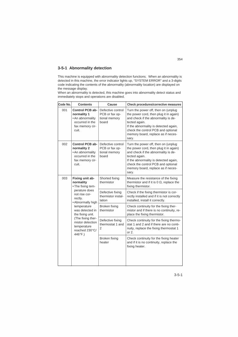
354
3-5-1 Abnormality detection
This machine is equipped with abnormality detection functions. When an abnormality isdetected in this machine, the error indicator lights up, “SYSTEM ERROR” and a 3-digitscode indicating the contents of the abnormality (abnormality location) are displayed onthe message display.When an abnormality is detected, this machine goes into abnormality detect status andimmediately stops and operations are disabled.
Code No. Contents Cause Check procedures/corrective measures
Turn the power off, then on (unplugthe power cord, then plug it in again)and check if the abnormality is de-tected again.If the abnormality is detected again,check the control PCB and optionalmemory board, replace as if neces-sary.
Turn the power off, then on (unplugthe power cord, then plug it in again)and check if the abnormality is de-tected again.If the abnormality is detected again,check the control PCB and optionalmemory board, replace as if neces-sary.
Measure the resistance of the fixingthermistor and if it is 0 Ω, replace thefixing thermistor.
Check if the fixing thermistor is cor-rectly installed and if it is not correctlyinstalled, install it correctly.
Check continuity for the fixing ther-mistor and if there is no continuity, re-place the fixing thermistor.
Check continuity for the fixing thermo-stat 1 and 2 and if there are no conti-nuity, replace the fixing thermostat 1or 2.
Check continuity for the fixing heaterand if it is no continuity, replace thefixing heater.
Control PCB ab-normality 1• An abnormalityoccurred in thefax memory cir-cuit.
Control PCB ab-normality 2• An abnormalityoccurred in thefax memory cir-cuit.
Fixing unit ab-normality• The fixing tem-perature doesnot rise cor-rectly.
• Abnormally hightemperaturewas detected inthe fixing unit.(The fixing ther-mistor detectiontemperaturereached 230°C/446°F.)
001
002
003
Defective controlPCB or fax op-tional memoryboard
Defective controlPCB or fax op-tional memoryboard
Shorted fixingthermistor
Defective fixingthermistor instal-lation
Broken fixingthermistor
Defective fixingthermostat 1 and2
Broken fixingheater
3-5-1
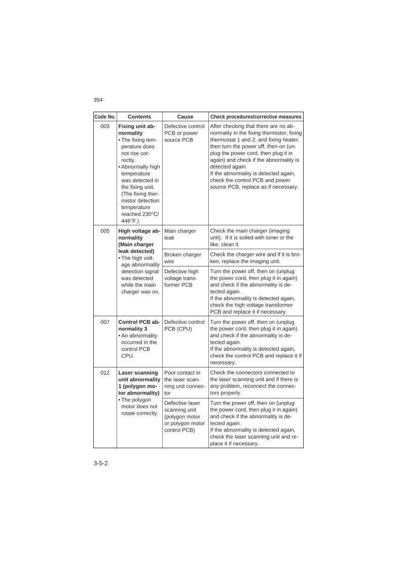
354
003
005
007
012
Code No. Contents Cause Check procedures/corrective measures
Fixing unit ab-normality• The fixing tem-perature doesnot rise cor-rectly.
• Abnormally hightemperaturewas detected inthe fixing unit.(The fixing ther-mistor detectiontemperaturereached 230°C/446°F.)
High voltage ab-normality(Main chargerleak detected)• The high volt-age abnormalitydetection signalwas detectedwhile the maincharger was on.
Control PCB ab-normality 3• An abnormalityoccurred in thecontrol PCBCPU.
Laser scanningunit abnormality1 (polygon mo-tor abnormality)• The polygonmotor does notrotate correctly.
Defective controlPCB or powersource PCB
Main chargerleak
Broken chargerwire
Defective highvoltage trans-former PCB
Defective controlPCB (CPU)
Poor contact inthe laser scan-ning unit connec-tor
Defective laserscanning unit(polygon motoror polygon motorcontrol PCB)
After checking that there are no ab-normality in the fixing thermistor, fixingthermostat 1 and 2, and fixing heater,then turn the power off, then on (un-plug the power cord, then plug it inagain) and check if the abnormality isdetected again.If the abnormality is detected again,check the control PCB and powersource PCB, replace as if necessary.
Check the main charger (imagingunit). If it is soiled with toner or thelike, clean it.
Check the charger wire and if it is bro-ken, replace the imaging unit.
Turn the power off, then on (unplugthe power cord, then plug it in again)and check if the abnormality is de-tected again.If the abnormality is detected again,check the high voltage transformerPCB and replace it if necessary.
Turn the power off, then on (unplugthe power cord, then plug it in again)and check if the abnormality is de-tected again.If the abnormality is detected again,check the control PCB and replace it ifnecessary.
Check the connectors connected tothe laser scanning unit and if there isany problem, reconnect the connec-tors properly.
Turn the power off, then on (unplugthe power cord, then plug it in again)and check if the abnormality is de-tected again.If the abnormality is detected again,check the laser scanning unit and re-place it if necessary.
3-5-2

354
Code No. Contents Cause Check procedures/corrective measures
013
014
015
Laser scanningunit abnormality2 (laser abnor-mality)• No laser beamis generatedfrom the laserdiode.
Control PCB ab-normality 4• An abnormalityoccurred in theprint memorycircuit.
Control PCB ab-normality 5• An abnormalityoccurred in theprinting/printermemory circuit.
Poor contact inthe laser scan-ning unit connec-tor
Defective laserscanning unit (la-ser diode PCB)
Defective controlPCB
Defective expan-sion memory(SIMM) installa-tion
Defective controlPCB or expan-sion memory(SIMM)
Check the connectors connected tothe laser scanning unit and if there isany problem, reconnect the connec-tors properly.
Turn the power off, then on (unplugthe power cord, then plug it in again)and check if the abnormality is de-tected again.If the abnormality is detected again,check the laser scanning unit and re-place it if necessary.
Turn the power off, then on (unplugthe power cord, then plug it in again)and check if the abnormality is de-tected again.If the abnormality is detected again,check the control PCB and replace it ifnecessary.
Check if the expansion memory(SIMM) is installed correctly and ifthere is any problem, reinstall it cor-rectly.
Turn the power off, then on (unplugthe power cord, then plug it in again)and check if the abnormality is de-tected again.If the abnormality is detected again,check the control PCB and expansionmemory (SIMM), replace as if neces-sary.
3-5-3
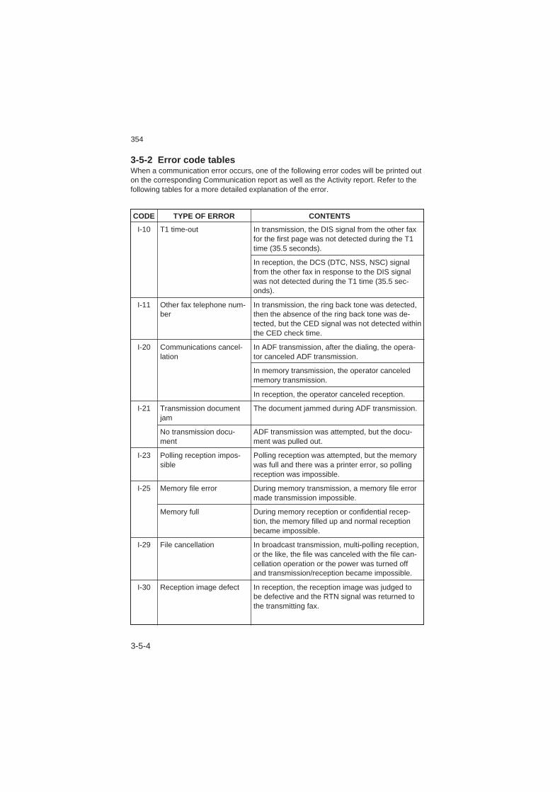
354
CODE TYPE OF ERROR CONTENTS
I-10
I-11
I-20
I-21
I-23
I-25
I-29
I-30
T1 time-out
Other fax telephone num-ber
Communications cancel-lation
Transmission documentjam
No transmission docu-ment
Polling reception impos-sible
Memory file error
Memory full
File cancellation
Reception image defect
In transmission, the DIS signal from the other faxfor the first page was not detected during the T1time (35.5 seconds).
In reception, the DCS (DTC, NSS, NSC) signalfrom the other fax in response to the DIS signalwas not detected during the T1 time (35.5 sec-onds).
In transmission, the ring back tone was detected,then the absence of the ring back tone was de-tected, but the CED signal was not detected withinthe CED check time.
In ADF transmission, after the dialing, the opera-tor canceled ADF transmission.
In memory transmission, the operator canceledmemory transmission.
In reception, the operator canceled reception.
The document jammed during ADF transmission.
ADF transmission was attempted, but the docu-ment was pulled out.
Polling reception was attempted, but the memorywas full and there was a printer error, so pollingreception was impossible.
During memory transmission, a memory file errormade transmission impossible.
During memory reception or confidential recep-tion, the memory filled up and normal receptionbecame impossible.
In broadcast transmission, multi-polling reception,or the like, the file was canceled with the file can-cellation operation or the power was turned offand transmission/reception became impossible.
In reception, the reception image was judged tobe defective and the RTN signal was returned tothe transmitting fax.
3-5-2 Error code tablesWhen a communication error occurs, one of the following error codes will be printed outon the corresponding Communication report as well as the Activity report. Refer to thefollowing tables for a more detailed explanation of the error.
3-5-4
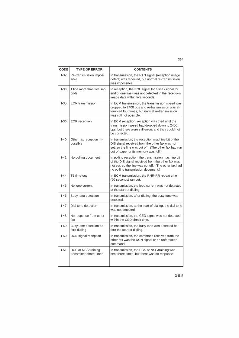
354
Re-transmission impos-sible
1 line more than five sec-onds
EOR transmission
EOR reception
Other fax reception im-possible
No polling document
T5 time-out
No loop current
Busy tone detection
Dial tone detection
No response from otherfax
Busy tone detection be-fore dialing
DCN signal reception
DCS or NSS/trainingtransmitted three times
CODE TYPE OF ERROR CONTENTS
I-32
I-33
I-35
I-36
I-40
I-41
I-44
I-45
I-46
I-47
I-48
I-49
I-50
I-51
In transmission, the RTN signal (reception imagedefect) was received, but normal re-transmissionwas impossible.
In reception, the EOL signal for a line (signal forend of one line) was not detected in the receptionimage data within five seconds.
In ECM transmission, the transmission speed wasdropped to 2400 bps and re-transmission was at-tempted four times, but normal re-transmissionwas still not possible.
In ECM reception, reception was tried until thetransmission speed had dropped down to 2400bps, but there were still errors and they could notbe corrected.
In transmission, the reception machine bit of theDIS signal received from the other fax was notset, so the line was cut off. (The other fax had runout of paper or its memory was full.)
In polling reception, the transmission machine bitof the DIS signal received from the other fax wasnot set, so the line was cut off. (The other fax hadno polling transmission document.)
In ECM transmission, the RNR-RR repeat time(60 seconds) ran out.
In transmission, the loop current was not detectedat the start of dialing.
In transmission, after dialing, the busy tone wasdetected.
In transmission, at the start of dialing, the dial tonewas not detected.
In transmission, the CED signal was not detectedwithin the CED check time.
In transmission, the busy tone was detected be-fore the start of dialing.
In transmission, the command received from theother fax was the DCN signal or an unforeseencommand.
In transmission, the DCS or NSS/training wassent three times, but there was no response.
3-5-5
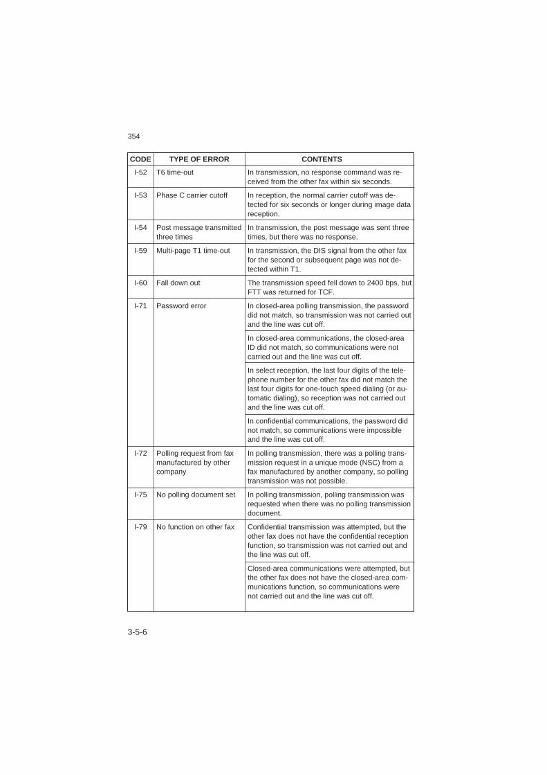
354
CODE TYPE OF ERROR CONTENTS
I-52
I-53
I-54
I-59
I-60
I-71
I-72
I-75
I-79
T6 time-out
Phase C carrier cutoff
Post message transmittedthree times
Multi-page T1 time-out
Fall down out
Password error
Polling request from faxmanufactured by othercompany
No polling document set
No function on other fax
In transmission, no response command was re-ceived from the other fax within six seconds.
In reception, the normal carrier cutoff was de-tected for six seconds or longer during image datareception.
In transmission, the post message was sent threetimes, but there was no response.
In transmission, the DIS signal from the other faxfor the second or subsequent page was not de-tected within T1.
The transmission speed fell down to 2400 bps, butFTT was returned for TCF.
In closed-area polling transmission, the passworddid not match, so transmission was not carried outand the line was cut off.
In closed-area communications, the closed-areaID did not match, so communications were notcarried out and the line was cut off.
In select reception, the last four digits of the tele-phone number for the other fax did not match thelast four digits for one-touch speed dialing (or au-tomatic dialing), so reception was not carried outand the line was cut off.
In confidential communications, the password didnot match, so communications were impossibleand the line was cut off.
In polling transmission, there was a polling trans-mission request in a unique mode (NSC) from afax manufactured by another company, so pollingtransmission was not possible.
In polling transmission, polling transmission wasrequested when there was no polling transmissiondocument.
Confidential transmission was attempted, but theother fax does not have the confidential receptionfunction, so transmission was not carried out andthe line was cut off.
Closed-area communications were attempted, butthe other fax does not have the closed-area com-munications function, so communications werenot carried out and the line was cut off.
3-5-6
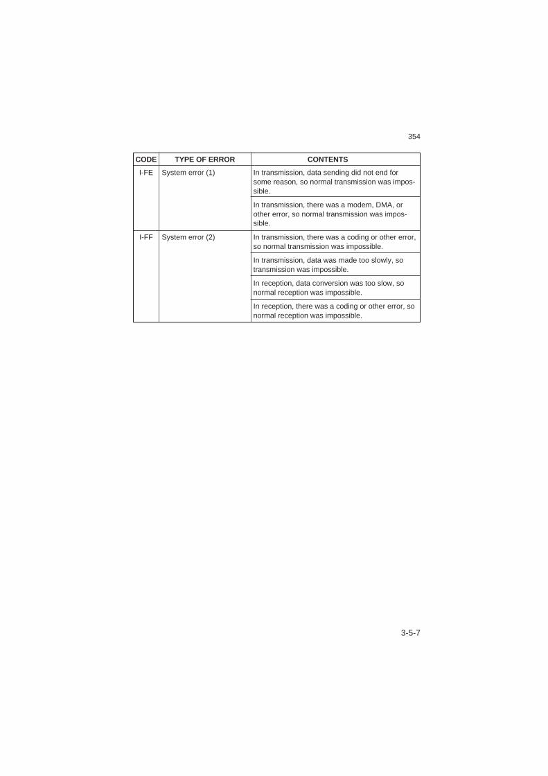
354
CODE TYPE OF ERROR CONTENTS
I-FE
I-FF
System error (1)
System error (2)
In transmission, data sending did not end forsome reason, so normal transmission was impos-sible.
In transmission, there was a modem, DMA, orother error, so normal transmission was impos-sible.
In transmission, there was a coding or other error,so normal transmission was impossible.
In transmission, data was made too slowly, sotransmission was impossible.
In reception, data conversion was too slow, sonormal reception was impossible.
In reception, there was a coding or other error, sonormal reception was impossible.
3-5-7
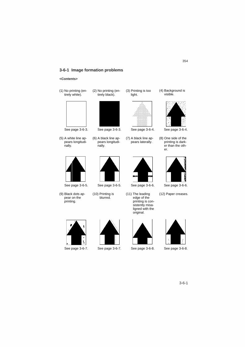
354
3-6-1
See page 3-6-3. See page 3-6-3. See page 3-6-4. See page 3-6-4.
(1) No printing (en-tirely white).
(2) No printing (en-tirely black).
(3) Printing is too light.
(4) Background is visible.
See page 3-6-5. See page 3-6-5. See page 3-6-6. See page 3-6-6.
(5) A white line ap-pears longitudi-nally.
(6) A black line ap-pears longitudi-nally.
(7) A black line ap-pears laterally.
(8) One side of the printing is dark-er than the oth-er.
See page 3-6-7. See page 3-6-7. See page 3-6-8. See page 3-6-8.
(9) Black dots ap-pear on the printing.
(10) Printing is blurred.
(11) The leading edge of the printing is con-sistently misa-ligned with the original.
(12) Paper creases.
3-6-1 Image formation problems
<Contents>
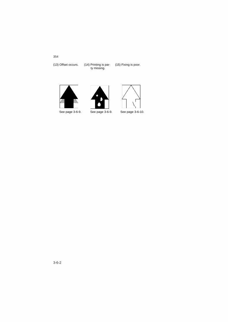
354
3-6-2
See page 3-6-9. See page 3-6-9. See page 3-6-10.
(13) Offset occurs. (14) Printing is par-ty missing.
(15) Fixing is poor.
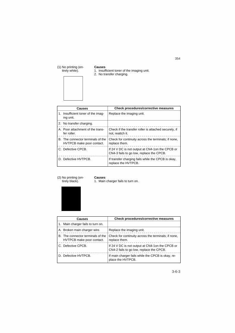
354
3-6-3
(1) No printing (en-tirely white).
Causes1. Insufficient toner of the imaging unit.2. No transfer charging.
Insufficient toner of the imag-ing unit.
No transfer charging.
Poor attachment of the trans-fer roller.
The connector terminals of the HVTPCB make poor contact.
Defective CPCB.
Defective HVTPCB.
Replace the imaging unit.
Check if the transfer roller is attached securely, if not, reattch it.
Check for continuity across the terminals; if none, replace them.
If 24 V DC is not output at CN4-1on the CPCB or CN4-3 fails to go low, replace the CPCB.
If transfer charging fails while the CPCB is okay, replace the HVTPCB.
1.
2.
A.
B.
C.
D.
Causes Check procedures/corrective measures
(2) No printing (en-tirely black).
Causes1. Main charger fails to turn on.
Replace the imaging unit.
Check for continuity across the terminals; if none, replace them.
If 24 V DC is not output at CN4-1on the CPCB or CN4-2 fails to go low, replace the CPCB.
If main charger fails while the CPCB is okay, re-place the HVTPCB.
1.
A.
B.
C.
D.
Main charger fails to turn on.
Broken main charger wire.
The connector terminals of the HVTPCB make poor contact.
Defective CPCB.
Defective HVTPCB.
Causes Check procedures/corrective measures
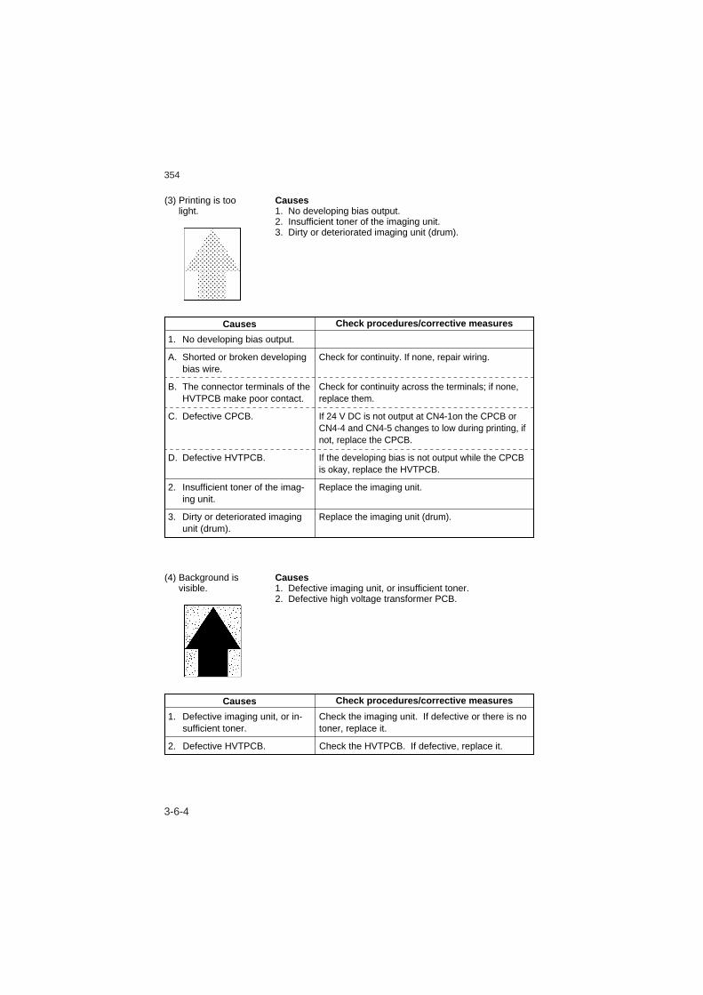
354
3-6-4
(3) Printing is too light.
Causes1. No developing bias output.2. Insufficient toner of the imaging unit.3. Dirty or deteriorated imaging unit (drum).
No developing bias output.
Shorted or broken developing bias wire.
The connector terminals of the HVTPCB make poor contact.
Defective CPCB.
Defective HVTPCB.
Insufficient toner of the imag-ing unit.
Dirty or deteriorated imaging unit (drum).
Check for continuity. If none, repair wiring.
Check for continuity across the terminals; if none, replace them.
If 24 V DC is not output at CN4-1on the CPCB or CN4-4 and CN4-5 changes to low during printing, if not, replace the CPCB.
If the developing bias is not output while the CPCB is okay, replace the HVTPCB.
Replace the imaging unit.
Replace the imaging unit (drum).
1.
A.
B.
C.
D.
2.
3.
Causes Check procedures/corrective measures
(4) Background is visible.
Causes1. Defective imaging unit, or insufficient toner.2. Defective high voltage transformer PCB.
Defective imaging unit, or in-sufficient toner.
Defective HVTPCB.
Check the imaging unit. If defective or there is no toner, replace it.
Check the HVTPCB. If defective, replace it.
1.
2.
Causes Check procedures/corrective measures
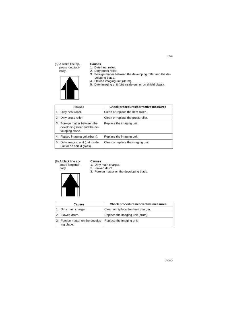
354
3-6-5
(5) A white line ap-pears longitudi-nally.
Causes1. Dirty heat roller.2. Dirty press roller.3. Foreign matter between the developing roller and the de-
veloping blade.4. Flawed imaging unit (drum).5. Dirty imaging unit (dirt inside unit or on shield glass).
Dirty heat roller.
Dirty press roller.
Foreign matter between the developing roller and the de-veloping blade.
Flawed imaging unit (drum).
Dirty imaging unit (dirt inside unit or on shield glass).
Clean or replace the heat roller.
Clean or replace the press roller.
Replace the imaging unit.
Replace the imaging unit.
Clean or replace the imaging unit.
1.
2.
3.
4.
5.
Causes Check procedures/corrective measures
Clean or replace the main charger.
Replace the imaging unit (drum).
Replace the imaging unit.
(6) A black line ap-pears longitudi-nally.
Causes1. Dirty main charger.2. Flawed drum.3. Foreign matter on the developing blade.
Dirty main charger.
Flawed drum.
Foreign matter on the develop-ing blade.
1.
2.
3.
Causes Check procedures/corrective measures
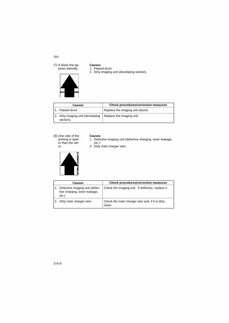
354
3-6-6
(7) A black line ap-pears laterally.
Causes1. Flawed drum.2. Dirty imaging unit (developing section).
Flawed drum.
Dirty imaging unit (developing section).
Replace the imaging unit (drum).
Replace the imaging unit.
1.
2.
Causes Check procedures/corrective measures
(8) One side of the printing is dark-er than the oth-er.
Causes1. Defective imaging unit (defective charging, toner leakage,
etc.)2. Dirty main charger wire.
Defective imaging unit (defec-tive charging, toner leakage, etc.)
Dirty main charger wire.
Check the imaging unit. If defective, replace it.
Check the main charger wire and, if it is dirty, clean.
1.
2.
Causes Check procedures/corrective measures
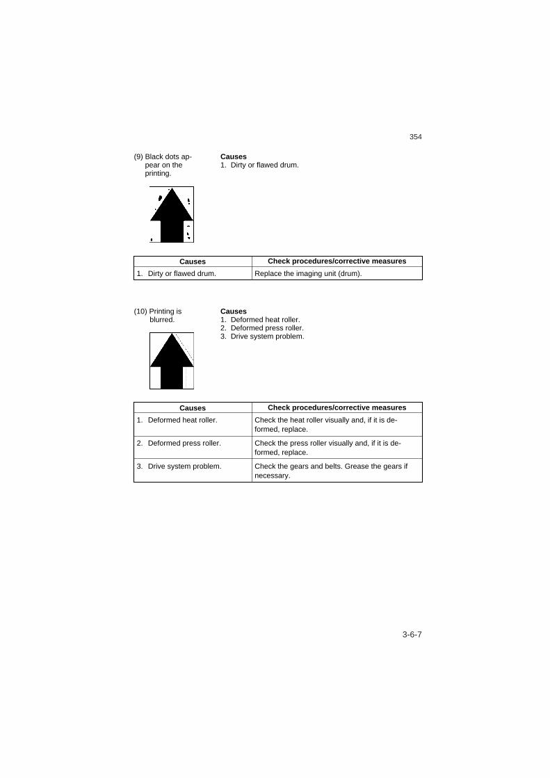
354
3-6-7
(9) Black dots ap-pear on the printing.
Causes1. Dirty or flawed drum.
Dirty or flawed drum. Replace the imaging unit (drum).1.
Causes Check procedures/corrective measures
(10) Printing is blurred.
Causes1. Deformed heat roller.2. Deformed press roller.3. Drive system problem.
Deformed heat roller.
Deformed press roller.
Drive system problem.
Check the heat roller visually and, if it is de-formed, replace.
Check the press roller visually and, if it is de-formed, replace.
Check the gears and belts. Grease the gears if necessary.
1.
2.
3.
Causes Check procedures/corrective measures

354
3-6-8
(11) The leading edge of the printing is con-sistently misa-ligned with the original.
Causes1. Misadjusted paper leading edge registration timing.
Misadjusted paper leading edge registration timing.
Readjust the paper leading edge registration tim-ing. (see page 3-3-44)
1.
Causes Check procedures/corrective measures
(12) Paper creases. Causes1. Paper curled.2. Paper damp.3. Defective fixing press springs.
Paper curled.
Paper damp.
Defective fixing press prings.
Check the paper storage conditions. If any, re-place the paper.
Check the paper storage conditions. If any, re-place the paper.
Replace the fixing press springs.
1.
2.
3.
Causes Check procedures/corrective measures
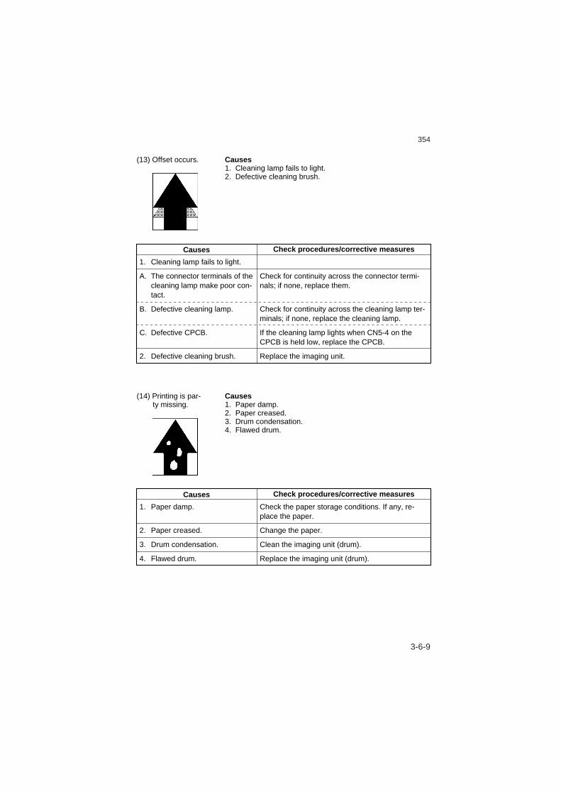
354
3-6-9
(13) Offset occurs. Causes1. Cleaning lamp fails to light.2. Defective cleaning brush.
Cleaning lamp fails to light.
The connector terminals of the cleaning lamp make poor con-tact.
Defective cleaning lamp.
Defective CPCB.
Defective cleaning brush.
Check for continuity across the connector termi-nals; if none, replace them.
Check for continuity across the cleaning lamp ter-minals; if none, replace the cleaning lamp.
If the cleaning lamp lights when CN5-4 on the CPCB is held low, replace the CPCB.
Replace the imaging unit.
1.
A.
B.
C.
2.
Causes Check procedures/corrective measures
(14) Printing is par-ty missing.
Causes1. Paper damp.2. Paper creased.3. Drum condensation.4. Flawed drum.
Paper damp.
Paper creased.
Drum condensation.
Flawed drum.
Check the paper storage conditions. If any, re-place the paper.
Change the paper.
Clean the imaging unit (drum).
Replace the imaging unit (drum).
1.
2.
3.
4.
Causes Check procedures/corrective measures

354
3-6-10
(15) Fixing is poor. Causes1. Wrong paper.2. Defective fixing press springs.3. Flawed heat roller.4. Flawed press roller.
Wrong paper.
Defective fixing press springs.
Flawed heat roller.
Flawed press roller.
Check if the paper meets specifications.
Replace the fixing press springs.
Replace the heat roller.
Replace the press roller.
1.
2.
3.
4.
Causes Check procedures/corrective measures

354
3-6-11
3-6-2 Paper jams
Check visually and remove it, if any.
If CN17-2 on the CPCB remains lowor high when the paper feed switch isturned on and off, replace the paperfeed switch.
If CN2-3 on the CPCB remains low orhigh when the eject switch is turnedon and off, replace the eject switch.
If CN11-14 on the CPCB remains lowor high when the document detectionswitch is turned on and off, replacethe document detection switch.
If CN11-11 on the CPCB remains lowor high when the ADF timing switch isturned on and off, replace the ADFtiming switch.
Check and remedy. (Replace the padguide spring if deformed.)
Check visually and clean or replace.(see page 3-3-15)
Check and remedy. (Replace thecrimp-style spring if deformed.)
Check and remedy. (Replace thecrimp-style spring if deformed.)
Check visually and replace deformedpulley. (see page 3-3-5)
Check visually and clean or replace.(see page 3-3-7)
Problem Causes/check procedures Corrective measure
Error indicatorlamp lights.
A piece of paper torn iscaught around the paperfeed switch, eject switch,document detection switchor ADF timing switch.
Defective paper feed switch.
Defective eject switch.
Defective documentdetection switch.
Defective ADF timing switch.
Check if the ADF paper feedroller and ADF pad are incontact with each othercorrectly.
Check if the ADF pad is dirtyor deformed.
Check if the ADF conveyingroller and ADF upper pulleyare in contact with eachother correctly.
Check if the ADF eject rollerand ADF upper pulley are incontact with each othercorrectly.
Check if the paper feedpulley is deformed.
Check if the peper feed padis dirty or deformed.
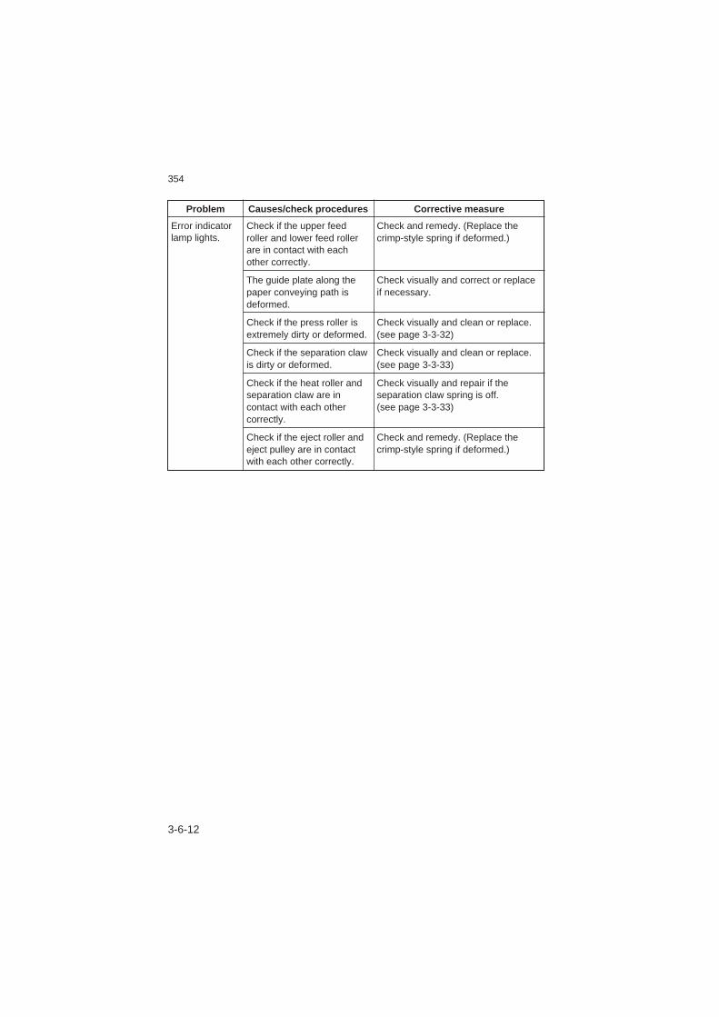
354
3-6-12
Problem Causes/check procedures Corrective measure
Error indicatorlamp lights.
Check if the upper feedroller and lower feed rollerare in contact with eachother correctly.
The guide plate along thepaper conveying path isdeformed.
Check if the press roller isextremely dirty or deformed.
Check if the separation clawis dirty or deformed.
Check if the heat roller andseparation claw are incontact with each othercorrectly.
Check if the eject roller andeject pulley are in contactwith each other correctly.
Check and remedy. (Replace thecrimp-style spring if deformed.)
Check visually and correct or replaceif necessary.
Check visually and clean or replace.(see page 3-3-32)
Check visually and clean or replace.(see page 3-3-33)
Check visually and repair if theseparation claw spring is off.(see page 3-3-33)
Check and remedy. (Replace thecrimp-style spring if deformed.)
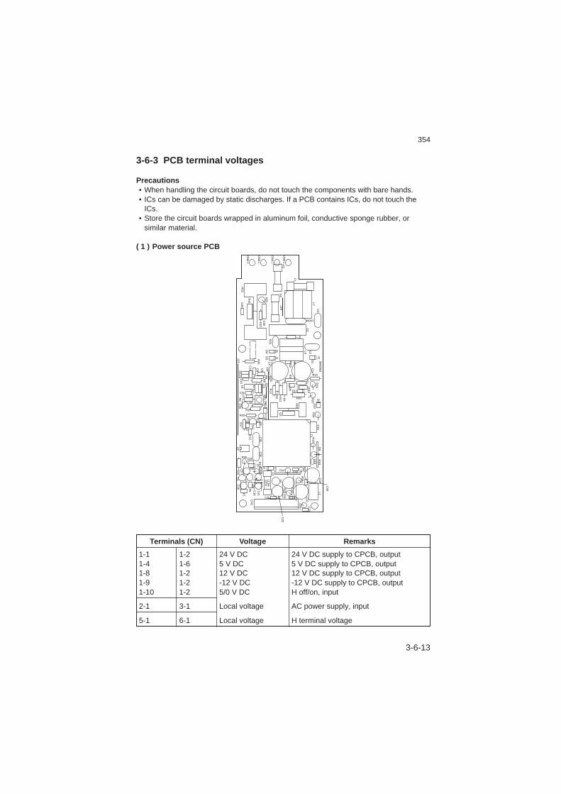
354
3-6-13
3-6-3 PCB terminal voltages
Precautions• When handling the circuit boards, do not touch the components with bare hands.• ICs can be damaged by static discharges. If a PCB contains ICs, do not touch the
ICs.• Store the circuit boards wrapped in aluminum foil, conductive sponge rubber, or
similar material.
( 1 ) Power source PCB
1-21-61-21-21-2
3-1
6-1
Terminals (CN) Voltage Remarks
24 V DC5 V DC12 V DC-12 V DC5/0 V DC
Local voltage
Local voltage
24 V DC supply to CPCB, output5 V DC supply to CPCB, output12 V DC supply to CPCB, output-12 V DC supply to CPCB, outputH off/on, input
AC power supply, input
H terminal voltage
1-11-41-81-91-10
2-1
5-1
CN
2-1
CN
3-1
CN
5-1
CN
6-1
F2
F4
J19
J18J22J16
R25
R27
R26
C11
J23R
17
D7T
H1Z2
C12 C
35C
36C
21
12.5A125V
C18
J20
L6
C13
D8
VR
1
R7
C8C
5C
6C
7C
39R
6C
10U
1
U2
R28
C17
R29
J21
R37
C23
C20
C19
C16
R18
D9
HS
3
R34
R22
C43
L1
L5C
28
D13
F3
D11
L2
C44
C27
F5
F6
CN
1
C34
R5
R15
R30
R36
C25
C22
C33
C32D14R35
C45
C9
R9R
8
TH
2C26
HS
2
C30
F1
MOV1
R21
R14
D12
D5
L7
C3
C1
R1
C2
C14
C15
T1
L4
D3
C4
D6
R10
R12 R
11R
4Q
1
R3
D2
R2
R16
R19
R20
R24
D10
HS
1
D4
R23
D1 3542803
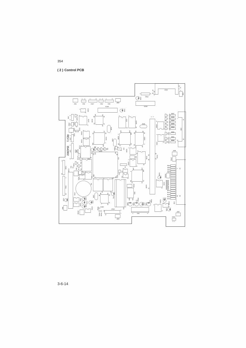
354
3-6-14
( 2 ) Control PCB
J006
22
402061
3919
21
21
113
2514
CN
8
D506
9
12
8
IC502
IC501
11
8
1
CN
19
IC500
IC202
IC200
IC207
IC4
C136
61316131
IC20
14
1920
3233
109108
144
X200
IC101
136
72
3233
4849
IC100
IC107
IC104
IC103
IC102
CN
51
1
12
2
12
4C
N14
CN
4
RE
V:1
3542802C
N7
CN
15C
N11
114
111
110
17
CN
20C
N18
D101
D105
TP
1
TP
2 VR
1D
2
D1
Q1
1
1
D100
D102
Q103
IC105
5
11
11
11
54
9 1617
73
815
5
IC10
108C
16
120121160
11 1
15 15
37144
D3
X100
1
51
7372
IC8
5
1
3736
52
1
6414
108109
144
1
1
1 5
8081
4140
5
72
JP400
IC400
IC5
ON
OF
F
SW
1
3736
73
81
11
8
IC403
IC402
X1
IC9
IC1
IC3
IC205
J004
14
11
3537
3638
72
D507
D504
D503
D505
D502
D501
D500
JP401
RA
400
C409
IC401
IC303
1
1
TP
001C001
C002
C006
7 1
C005
C301
X300
IC6
IC2
33
4849
3217
161
2221
C311
TP
302
TP
300
TP
301
C313
C315
C309
C337
C306
IC301
IC302
VR
300
Z101
J002
12
TP
002
IC304
CN
9
C3319
12
5
193618
1
CN16
B507
B506
B504
B505
B503
B502
B501
B500
J008
B413
B400
B401
B402
B411
B412
B416
B414
B415
J007
CN12
C332
B403B404B405B406B407B408B409B410
CN13
IC208
X500
CN1
J005
CN10
IC300
C225
J003CN6
IC106
CN2CN17CN3J001
Q104 IC11
D4
Q3Q2
IC7
+
+
+
+
+
++
+
+
+
+
+
+++
+
IC305

354
3-6-15
1-21-41-21-21-4
2-22-2
3-33-3
4-74-74-74-74-74-7
1-21-21-21-2
1-21-21-21-21-21-2
1-21-21-21-21-21-21-21-2
10-2110-2110-2110-2110-1510-2110-1510-2110-2110-2110-21
Terminals (CN) Voltage Remarks
24 V DC5 V DC12 V DC-12 V DC5/0 V DC
5 V DC5/0 V DC
5 V DC5/0 V DC
24 V DC24/0 V DC24/0 V DC24/0 V DC24/0 V DC5/0 V DC
24/0 V DC24 V DC24 V DC24/0 V DC
24/0 V DC (Pulse)24/0 V DC (Pulse)24 V DC24 V DC24/0 V DC (Pulse)24/0 V DC (Pulse)
5/0 V DC (Pulse)5/0 V DC0/5 V DC24 V DC5/0 V DC (Pulse)5 V DC5/0 V DC (Pulse)5/0 V DC (Pulse)
5/0 V DC5/0 V DC5/0 V DC5/0 V DC (Pulse)Audio frequency5/0 V DCAudio frequency5/0 V DC5/0 V DC5/0 V DC5/0 V DC
24 V DC power supply, input5 V DC power supply, input12 V DC power supply, input-12 V DC power supply, inputH off/on, output
5 V DC supply to ESW, outputESW off/on, input
5 V DC supply to TEDS, outputTEDS off/on, input
24 V DC supply to HVTPCB, outputHVTPCB main charger off/on, outputHVTPCB transfer charger off/on, outputHVTPCB developing bias1 off/on, outputHVTPCB developing bias2 off/on, outputMain charger leak signal, input
FSOL off/on, output24 V DC supply to FSOL, output24 V DC supply to CL, outputCL off/on, output
MM drive (A)MM drive (A)24 V DC supply to MM, output24 V DC supply to MM, outputMM drive (B)MM drive (B)
Polygon motor clock, outputPolygon motor sync, outputPolygon motor on/off, output24 V DC supply to LSU, outputBD sensor, input5 V DC supply to LSU, outputLaser on/off, outputLaser on permission, output
Line polarity detection, inputLine polarity detection, inputTEL/FAX switching, outputPulse dial, outputImage data, inputReception switching, outputImage data, outputTEL GND off/on, outputMute off/on, outputIncoming call off/on, inputTelephone off-hook off/on, input
1-11-31-51-61-7
2-12-3
3-13-2
4-14-24-34-44-54-6
5-15-25-35-4
6-16-26-36-46-56-6
7-17-27-37-57-67-77-97-10
10-110-210-310-410-510-610-710-810-910-1010-11
354-1
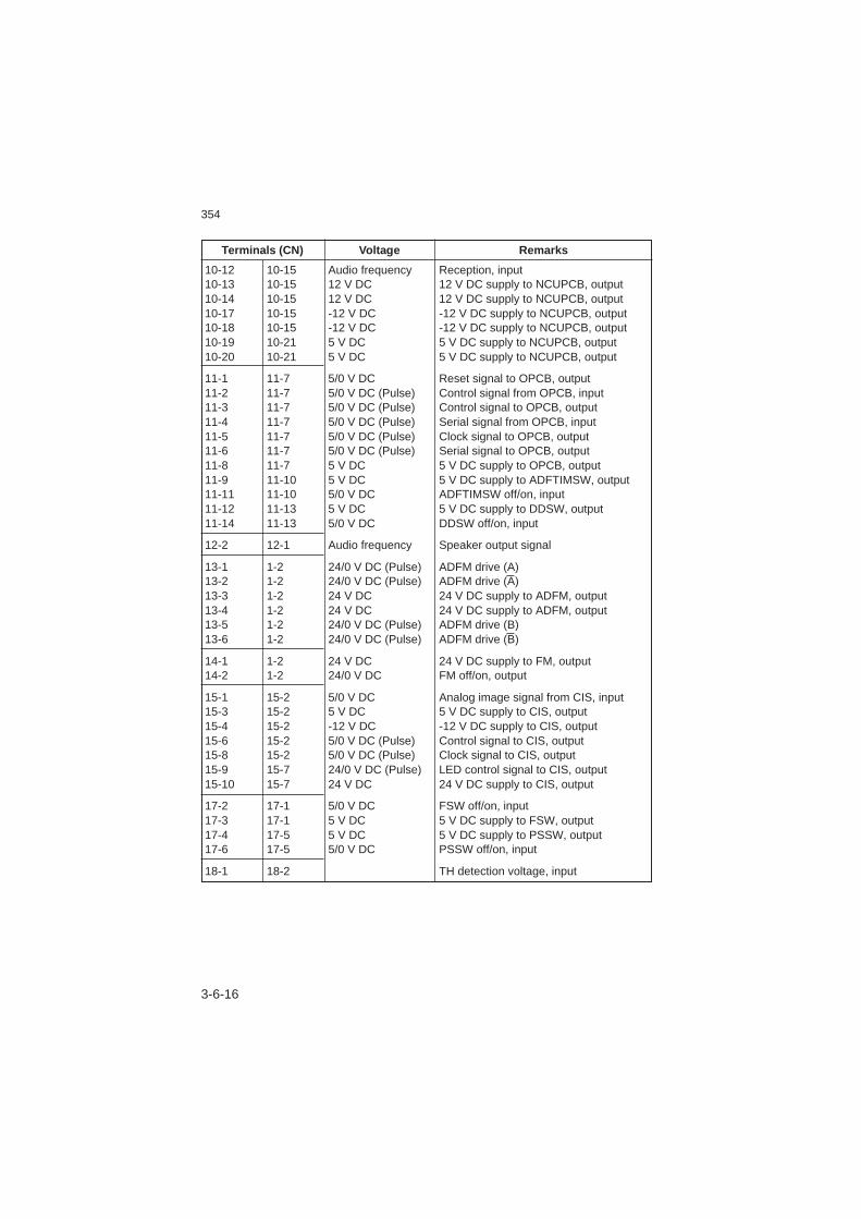
354
3-6-16
Terminals (CN) Voltage Remarks
10-1210-1310-1410-1710-1810-1910-20
11-111-211-311-411-511-611-811-911-1111-1211-14
12-2
13-113-213-313-413-513-6
14-114-2
15-115-315-415-615-815-915-10
17-217-317-417-6
18-1
10-1510-1510-1510-1510-1510-2110-21
11-711-711-711-711-711-711-711-1011-1011-1311-13
12-1
1-21-21-21-21-21-2
1-21-2
15-215-215-215-215-215-715-7
17-117-117-517-5
18-2
Reception, input12 V DC supply to NCUPCB, output12 V DC supply to NCUPCB, output-12 V DC supply to NCUPCB, output-12 V DC supply to NCUPCB, output5 V DC supply to NCUPCB, output5 V DC supply to NCUPCB, output
Reset signal to OPCB, outputControl signal from OPCB, inputControl signal to OPCB, outputSerial signal from OPCB, inputClock signal to OPCB, outputSerial signal to OPCB, output5 V DC supply to OPCB, output5 V DC supply to ADFTIMSW, outputADFTIMSW off/on, input5 V DC supply to DDSW, outputDDSW off/on, input
Speaker output signal
ADFM drive (A)ADFM drive (A)24 V DC supply to ADFM, output24 V DC supply to ADFM, outputADFM drive (B)ADFM drive (B)
24 V DC supply to FM, outputFM off/on, output
Analog image signal from CIS, input5 V DC supply to CIS, output-12 V DC supply to CIS, outputControl signal to CIS, outputClock signal to CIS, outputLED control signal to CIS, output24 V DC supply to CIS, output
FSW off/on, input5 V DC supply to FSW, output5 V DC supply to PSSW, outputPSSW off/on, input
TH detection voltage, input
Audio frequency12 V DC12 V DC-12 V DC-12 V DC5 V DC5 V DC
5/0 V DC5/0 V DC (Pulse)5/0 V DC (Pulse)5/0 V DC (Pulse)5/0 V DC (Pulse)5/0 V DC (Pulse)5 V DC5 V DC5/0 V DC5 V DC5/0 V DC
Audio frequency
24/0 V DC (Pulse)24/0 V DC (Pulse)24 V DC24 V DC24/0 V DC (Pulse)24/0 V DC (Pulse)
24 V DC24/0 V DC
5/0 V DC5 V DC-12 V DC5/0 V DC (Pulse)5/0 V DC (Pulse)24/0 V DC (Pulse)24 V DC
5/0 V DC5 V DC5 V DC5/0 V DC

354
3-6-17
( 3 ) Operation unit PCB
Terminals (CN) Voltage Remarks
1-11-31-41-51-61-71-8
1-21-21-21-21-21-21-2
5 V DC5/0 V DC (Pulse)5/0 V DC (Pulse)5/0 V DC (Pulse)5/0 V DC (Pulse)5/0 V DC (Pulse)5/0 V DC (Pulse)
5 V DC supply from CPCB, inputSerial signal to CPCB, outputClock signal from CPCB, inputSerial signal from CPCB, inputControl signal from CPCB, inputControl signal to CPCB, outputReset signal from CPCB, input
SW
4
SW
7
SW
10
SW
12
SW
28
SW
2
SW
5
SW
8
SW
11
SW
26S
W30
SW
25B
SW
25A
SW
23S
W24
L1
SW
32
SW
31
SW
29
SW
14
SW
18
SW
16
SW
20
SW
22
SW
13
SW
17
SW
15
SW
19
SW
21
SW
3
SW
6
SW
9SW
1
SW
27
JP38
JP1
JP6
JP4
JP8
JP15
JP9
JP16
JP5
JP10
JP14
R13
JP13
JP12
JP11EQ4
JP39JP
40JP47
JP49
JP30
JP28
JP48
JP44
JP41
JP42JP
43
JP31
JP32
JP3
JP7
JP17
JP18
JP19
JP2
JP45
JP46
JP37
JP36
JP23JP22JP21
JP34
JP33
JP35
JP27
JP25JP24
JP20
JP26
JP511 13CN2
2 14
JP50
R21
R25
R22
R23
R5R7
R4
R1C3
R3R6R2
R24
R8
R9
R17
R16
R12
R11
R14
LED
4R10
R15
R20
R19
R18
L3C
N1
L2
LED
8
LED
6
LED
5
LED
2LE
D3
LED
7
LED
1
EQ5
EQ6
EQ7
EQ1
EQ2
EQ3
C2
C1
C6
C13
C12C9
X1
C4
C11
C5
C7
C10 32 33
C8
JP29
1
IC1
64
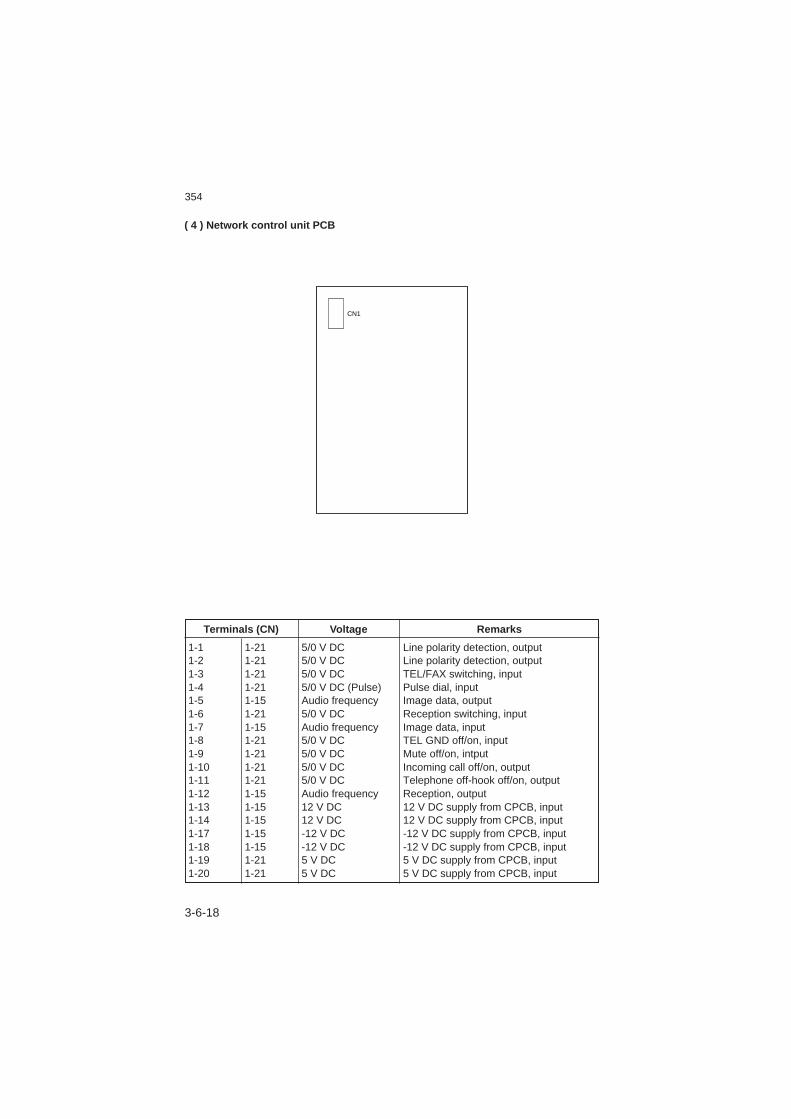
354
3-6-18
( 4 ) Network control unit PCB
Terminals (CN) Voltage Remarks
1-11-21-31-41-51-61-71-81-91-101-111-121-131-141-171-181-191-20
1-211-211-211-211-151-211-151-211-211-211-211-151-151-151-151-151-211-21
5/0 V DC5/0 V DC5/0 V DC5/0 V DC (Pulse)Audio frequency5/0 V DCAudio frequency5/0 V DC5/0 V DC5/0 V DC5/0 V DCAudio frequency12 V DC12 V DC-12 V DC-12 V DC5 V DC5 V DC
Line polarity detection, outputLine polarity detection, outputTEL/FAX switching, inputPulse dial, inputImage data, outputReception switching, inputImage data, inputTEL GND off/on, inputMute off/on, intputIncoming call off/on, outputTelephone off-hook off/on, outputReception, output12 V DC supply from CPCB, input12 V DC supply from CPCB, input-12 V DC supply from CPCB, input-12 V DC supply from CPCB, input5 V DC supply from CPCB, input5 V DC supply from CPCB, input
CN1
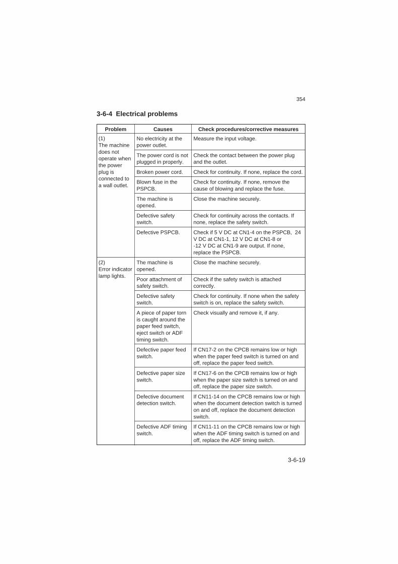
354
3-6-19
3-6-4 Electrical problems
Measure the input voltage.
Check the contact between the power plugand the outlet.
Check for continuity. If none, replace the cord.
Check for continuity. If none, remove thecause of blowing and replace the fuse.
Close the machine securely.
Check for continuity across the contacts. Ifnone, replace the safety switch.
Check if 5 V DC at CN1-4 on the PSPCB, 24V DC at CN1-1, 12 V DC at CN1-8 or-12 V DC at CN1-9 are output. If none,replace the PSPCB.
Close the machine securely.
Check if the safety switch is attachedcorrectly.
Check for continuity. If none when the safetyswitch is on, replace the safety switch.
Check visually and remove it, if any.
If CN17-2 on the CPCB remains low or highwhen the paper feed switch is turned on andoff, replace the paper feed switch.
If CN17-6 on the CPCB remains low or highwhen the paper size switch is turned on andoff, replace the paper size switch.
If CN11-14 on the CPCB remains low or highwhen the document detection switch is turnedon and off, replace the document detectionswitch.
If CN11-11 on the CPCB remains low or highwhen the ADF timing switch is turned on andoff, replace the ADF timing switch.
Problem Causes Check procedures/corrective measures
(1)The machinedoes notoperate whenthe powerplug isconnected toa wall outlet.
(2)Error indicatorlamp lights.
No electricity at thepower outlet.
The power cord is notplugged in properly.
Broken power cord.
Blown fuse in thePSPCB.
The machine isopened.
Defective safetyswitch.
Defective PSPCB.
The machine isopened.
Poor attachment ofsafety switch.
Defective safetyswitch.
A piece of paper tornis caught around thepaper feed switch,eject switch or ADFtiming switch.
Defective paper feedswitch.
Defective paper sizeswitch.
Defective documentdetection switch.
Defective ADF timingswitch.

354
3-6-20
Problem Causes Check procedures/corrective measures
Defective eject switch.
Polygon motor of thelaser scanning unitproblem.
Poor contact in themain motor connectorterminals.
Defective CPCB.
Defective main motor.
Poor contact in thepaper feed solenoidconnector terminals.
Broken paper feedsolenoid coil.
Defective CPCB.
Poor contact in thecooling fan motorconnector terminals.
Defective CPCB.
Defective cooling fanmotor.
Poor contact in theADF motor connectorterminals.
Defective CPCB.
If CN2-3 on the CPCB remains low or highwhen the eject switch is turned on and off,replace the eject switch.
Check for connection of the CPCB and thelaser scanning unit. If not, replace the laserscanning unit.
Check for the continuity across the connectorterminals. If none, replace the main motorconnector terminals.
Check if 24 V DC is output at CN6-3 andCN6-4 on the CPCB, or if the motor drive coilenergination pulse signals are present atCN6-1, 2, 5 and 6. If not, replace the CPCB.
If the main motor does not rotate while theCPCB is okay, replace the main motor.
Check for continuity across the connectorterminals. If none, replace them.
Check for continuity across the coil. If none,replace the paper feed solenoid.
Check if 24 V DC is not output at CN5-2 onthe CPCB, or if the paper feed solenoidoperates when CN5-1 on the CPCB held low.If so, replace the CPCB.
Check for continuity across the connectorterminals. If none, replace them.
Check if 24 V DC is not output at CN14-1 onthe CPCB, or if the cooling fan motor rotateswhen CN14-2 on the CPCB held low. If so,replace the CPCB.
If the cooling fan motor does not rotate whilethe CPCB is okay, replace the cooling fanmotor.
Check for continuity across the connectorterminals. If none, replace them.
Check if 24 V DC is output at CN13-3 andCN13-4 on the CPCB, or if the motor drive coilenergination pulse signals are present atCN13-1, 2, 5 and 6. If not, replace the CPCB.
(2)Error indicatorlamp lights.
(3)The mainmotor doesnot rotate.
(4)The paperfeed solenoiddoes notoperate.
(5)The coolingfan motordoes notrotate.
(6)The ADFmotor doesnot rotate.
354-1
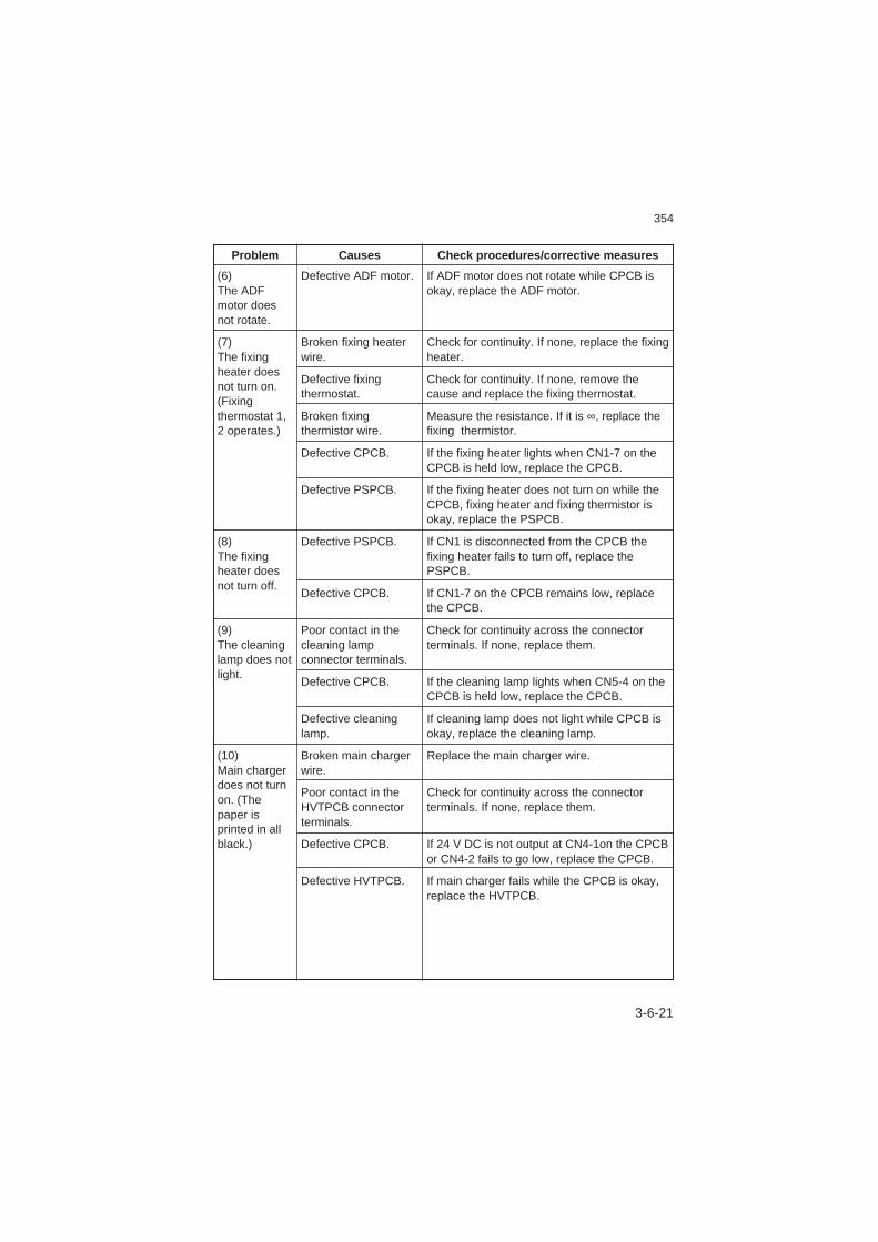
354
3-6-21
Problem Causes Check procedures/corrective measures
(6)The ADFmotor doesnot rotate.
(7)The fixingheater doesnot turn on.(Fixingthermostat 1,2 operates.)
(8)The fixingheater doesnot turn off.
(9)The cleaninglamp does notlight.
(10)Main chargerdoes not turnon. (Thepaper isprinted in allblack.)
Defective ADF motor.
Broken fixing heaterwire.
Defective fixingthermostat.
Broken fixingthermistor wire.
Defective CPCB.
Defective PSPCB.
Defective PSPCB.
Defective CPCB.
Poor contact in thecleaning lampconnector terminals.
Defective CPCB.
Defective cleaninglamp.
Broken main chargerwire.
Poor contact in theHVTPCB connectorterminals.
Defective CPCB.
Defective HVTPCB.
If ADF motor does not rotate while CPCB isokay, replace the ADF motor.
Check for continuity. If none, replace the fixingheater.
Check for continuity. If none, remove thecause and replace the fixing thermostat.
Measure the resistance. If it is ∞, replace thefixing thermistor.
If the fixing heater lights when CN1-7 on theCPCB is held low, replace the CPCB.
If the fixing heater does not turn on while theCPCB, fixing heater and fixing thermistor isokay, replace the PSPCB.
If CN1 is disconnected from the CPCB thefixing heater fails to turn off, replace thePSPCB.
If CN1-7 on the CPCB remains low, replacethe CPCB.
Check for continuity across the connectorterminals. If none, replace them.
If the cleaning lamp lights when CN5-4 on theCPCB is held low, replace the CPCB.
If cleaning lamp does not light while CPCB isokay, replace the cleaning lamp.
Replace the main charger wire.
Check for continuity across the connectorterminals. If none, replace them.
If 24 V DC is not output at CN4-1on the CPCBor CN4-2 fails to go low, replace the CPCB.
If main charger fails while the CPCB is okay,replace the HVTPCB.
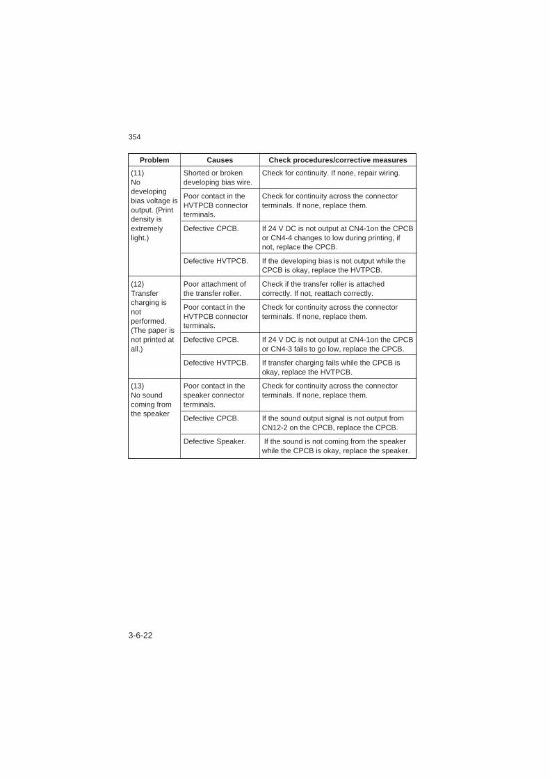
354
3-6-22
Problem Causes Check procedures/corrective measures
(11)Nodevelopingbias voltage isoutput. (Printdensity isextremelylight.)
(12)Transfercharging isnotperformed.(The paper isnot printed atall.)
(13)No soundcoming fromthe speaker
Shorted or brokendeveloping bias wire.
Poor contact in theHVTPCB connectorterminals.
Defective CPCB.
Defective HVTPCB.
Poor attachment ofthe transfer roller.
Poor contact in theHVTPCB connectorterminals.
Defective CPCB.
Defective HVTPCB.
Poor contact in thespeaker connectorterminals.
Defective CPCB.
Defective Speaker.
Check for continuity. If none, repair wiring.
Check for continuity across the connectorterminals. If none, replace them.
If 24 V DC is not output at CN4-1on the CPCBor CN4-4 changes to low during printing, ifnot, replace the CPCB.
If the developing bias is not output while theCPCB is okay, replace the HVTPCB.
Check if the transfer roller is attachedcorrectly. If not, reattach correctly.
Check for continuity across the connectorterminals. If none, replace them.
If 24 V DC is not output at CN4-1on the CPCBor CN4-3 fails to go low, replace the CPCB.
If transfer charging fails while the CPCB isokay, replace the HVTPCB.
Check for continuity across the connectorterminals. If none, replace them.
If the sound output signal is not output fromCN12-2 on the CPCB, replace the CPCB.
If the sound is not coming from the speakerwhile the CPCB is okay, replace the speaker.
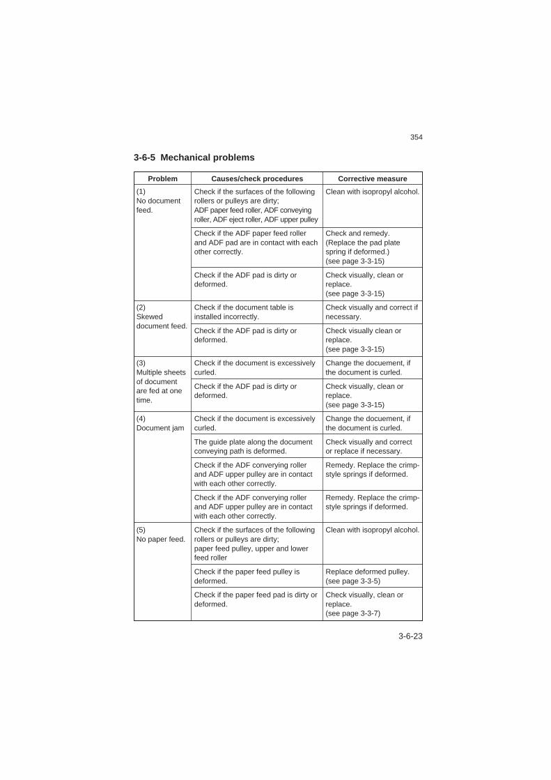
354
3-6-23
3-6-5 Mechanical problems
Clean with isopropyl alcohol.
Check and remedy.(Replace the pad platespring if deformed.)(see page 3-3-15)
Check visually, clean orreplace.(see page 3-3-15)
Check visually and correct ifnecessary.
Check visually clean orreplace.(see page 3-3-15)
Change the docuement, ifthe document is curled.
Check visually, clean orreplace.(see page 3-3-15)
Change the docuement, ifthe document is curled.
Check visually and corrector replace if necessary.
Remedy. Replace the crimp-style springs if deformed.
Remedy. Replace the crimp-style springs if deformed.
Clean with isopropyl alcohol.
Replace deformed pulley.(see page 3-3-5)
Check visually, clean orreplace.(see page 3-3-7)
Problem Causes/check procedures Corrective measure
(1)No documentfeed.
(2)Skeweddocument feed.
(3)Multiple sheetsof documentare fed at onetime.
(4)Document jam
(5)No paper feed.
Check if the surfaces of the followingrollers or pulleys are dirty;ADF paper feed roller, ADF conveyingroller, ADF eject roller, ADF upper pulley
Check if the ADF paper feed rollerand ADF pad are in contact with eachother correctly.
Check if the ADF pad is dirty ordeformed.
Check if the document table isinstalled incorrectly.
Check if the ADF pad is dirty ordeformed.
Check if the document is excessivelycurled.
Check if the ADF pad is dirty ordeformed.
Check if the document is excessivelycurled.
The guide plate along the documentconveying path is deformed.
Check if the ADF converying rollerand ADF upper pulley are in contactwith each other correctly.
Check if the ADF converying rollerand ADF upper pulley are in contactwith each other correctly.
Check if the surfaces of the followingrollers or pulleys are dirty;paper feed pulley, upper and lowerfeed roller
Check if the paper feed pulley isdeformed.
Check if the paper feed pad is dirty ordeformed.
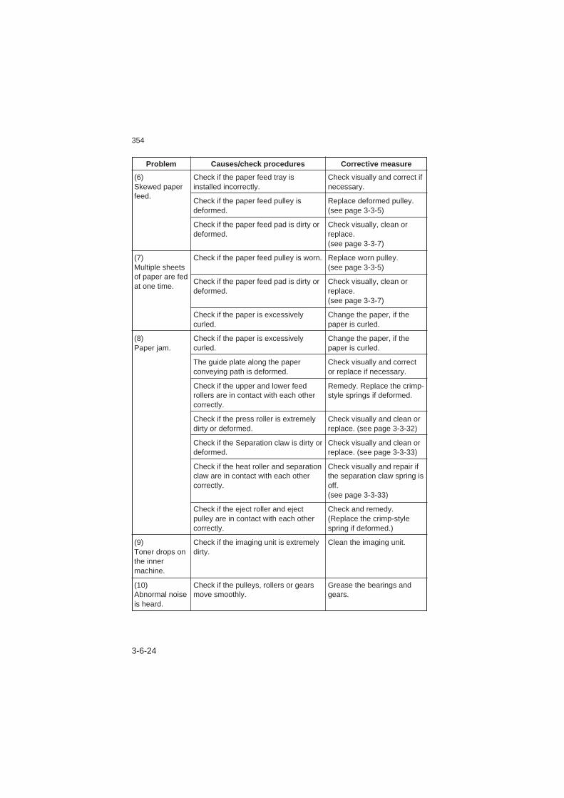
354
3-6-24
Problem Causes/check procedures Corrective measure
(6)Skewed paperfeed.
(7)Multiple sheetsof paper are fedat one time.
(8)Paper jam.
(9)Toner drops onthe innermachine.
(10)Abnormal noiseis heard.
Check if the paper feed tray isinstalled incorrectly.
Check if the paper feed pulley isdeformed.
Check if the paper feed pad is dirty ordeformed.
Check if the paper feed pulley is worn.
Check if the paper feed pad is dirty ordeformed.
Check if the paper is excessivelycurled.
Check if the paper is excessivelycurled.
The guide plate along the paperconveying path is deformed.
Check if the upper and lower feedrollers are in contact with each othercorrectly.
Check if the press roller is extremelydirty or deformed.
Check if the Separation claw is dirty ordeformed.
Check if the heat roller and separationclaw are in contact with each othercorrectly.
Check if the eject roller and ejectpulley are in contact with each othercorrectly.
Check if the imaging unit is extremelydirty.
Check if the pulleys, rollers or gearsmove smoothly.
Check visually and correct ifnecessary.
Replace deformed pulley.(see page 3-3-5)
Check visually, clean orreplace.(see page 3-3-7)
Replace worn pulley.(see page 3-3-5)
Check visually, clean orreplace.(see page 3-3-7)
Change the paper, if thepaper is curled.
Change the paper, if thepaper is curled.
Check visually and corrector replace if necessary.
Remedy. Replace the crimp-style springs if deformed.
Check visually and clean orreplace. (see page 3-3-32)
Check visually and clean orreplace. (see page 3-3-33)
Check visually and repair ifthe separation claw spring isoff.(see page 3-3-33)
Check and remedy.(Replace the crimp-stylespring if deformed.)
Clean the imaging unit.
Grease the bearings andgears.