Embed Size (px)
Citation preview

Manufacturing & Distribution WorldwideAmericas +1-401-463-5605Europe +44-1737-222-258 Asia-Pacific +852-2649-7183 [email protected] www.aimsolder.com
Alloys Alloys •• Chemistries Chemistries ••Data Data •• Training Training •• ConsultationConsultation
LeadLead--Free Free Soldering GuideSoldering Guide
01.13.0306.25..03
LEAD
4 Time SMT Vision Award Winner
AIM has the lead-free products and process knowledge required to help your company in the transition to lead-free soldering in the most logical and economical ways possible.
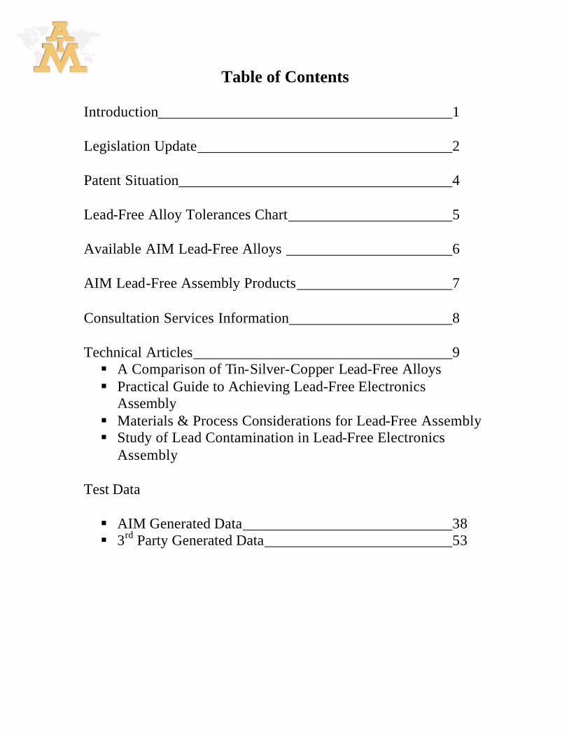
Table of Contents
Introduction 1 Legislation Update 2 Patent Situation 4 Lead-Free Alloy Tolerances Chart 5 Available AIM Lead-Free Alloys 6 AIM Lead-Free Assembly Products 7 Consultation Services Information 8 Technical Articles 9 § A Comparison of Tin-Silver-Copper Lead-Free Alloys § Practical Guide to Achieving Lead-Free Electronics
Assembly § Materials & Process Considerations for Lead-Free Assembly § Study of Lead Contamination in Lead-Free Electronics
Assembly Test Data § AIM Generated Data 38 § 3rd Party Generated Data 53
Introduction The issue of lead-free soldering has piqued a great deal of interest in the electronics assembly industry as of late. What was once an issue that seemed too far away to worry about has become a pressing reality. In order to avoid confusion, last minute panic, and a misunderstanding of how the issue of lead-free soldering will affect the industry and individuals users of solders, it is necessary for all suppliers and assemblers to become educated in this matter.
Lead-Free Soldering- Why? There is no easy answer to why the industry has become so pre-occupied with lead-free solders as of late, since there is no imminent legislation; the most simple explanation is FEAR: Fear of (potential) Legislation, Fear of Trade Barriers, and Fear of Competition. It is likely that most of the companies currently concerned with the lead-free issue are motivated by a combination of these three. • The WEEE directive in Europe and similar mandates in Japan have instilled fear that a legislative body will
prohibit the use of lead in electronics soldering. • If a particular country disallows lead from electronics, then a de facto trade barrier is created between that
country and anyone not capable of providing lead-free electronics solutions. Of course, this also could take place between individual companies or industries.
• Some companies already are producing electronics products with lead-free solder alloys and marketing them as
such. This has led to fears of being caught behind in the marketing game.
Resistance to Lead-Free Soldering Along with the great interest in lead-free soldering has come much resistance to this potential change. The reasons for this change may be divided into two categories: cost and reliability concerns. As lead is one of the least expensive elements on earth, replacing it with virtually any other metal will raise the price. In addition, incidental costs should not be overlooked; the cost of educating and training company personnel on the use of lead-free alloys is not an inexpensive venture. Reliability issues are also a great concern in the lead-free issue. Although many of the lead-free alloys have demonstrated more-than-adequate reliability characteristics, engineers have developed a certain comfort factor with tin-lead over the last thirty years that will not be easy to emulate.
Lead-Free Solder Requirements In response to the aforementioned concerns, a great amount of effort has gone into the development of lead-free solders intended to be �viable� replacements for tin-lead solders. Although each of these alloys has its advantages and disadvantages, some alloys clearly stand out as the likely replacements for tin-lead for the majority of soldering applications.
NOW is the Time to Prepare Lead-free soldering seems to be more an issue of �when�, rather than �if�, anymore. In order to be prepared for the inevitable switch to lead-free soldering, companies should begin the search for suitable lead-free products and processes for their unique applications as soon as possible. Only when companies have hands-on experience with lead-free electronics assembly will there be complete confidence in the viability of lead-free soldering and an understanding of what to expect from this dramatic process change.
This booklet is intended to guide the future users of lead-free solders to the most appropriate lead-free alloys and processes for their applications. Please feel free to contact AIM at anytime so that we may be of assistance during this transition period. Whether you choose to implement CASTIN®, sample another lead-free alloy, or simply have a technical question to be answered, AIM is your source for the latest in lead-free soldering technology.
1
Legislation Update On Friday October 11, 2002 the EU approved The Waste From Electrical And Electronic Equipment (WEEE) and The Use Of Certain Hazardous Substances In Electrical And Electronic Equipment (RoHS) Directives. It has been decided that four heavy metals (lead, cadmium, mercury and hexavalent chromium) and the brominated flame retardants PBB and PBDE will be banned in new electronic equipment in the European Union from 1 July 2006. Existing national measures on these substances can continue to apply until that date, by which they have to be replaced by the new Community rules. Following is a summary of the Directives: Areas Affected
• These directives pertain to products manufactured and imported into European Community member states (currently Austria, Belgium, Denmark, Finland, France, Germany, Greece, Ireland, Italy, Luxembourg, Portugal, Spain, Sweden, the Netherlands and the UK).
Scope & Coverage
• Categories o Large household appliances o Small household appliances o IT & Telecommunication equipment o Consumer equipment o Lighting equipment o Electrical and electronic tools o Toys o Medical equipment systems (with the exception of all implanted and
infected products) o Monitoring and control instruments o Automatic dispensers
• The exemptions have not been changed. They remain: o Lead in high melting temperature type solders (i.e. tin- lead solder alloys
containing more than 85% lead) o Lead in glass in electronic components o Lead in piezoelectric devices o Lead in servers, storage and storage array systems (exempt until 2010) o Lead in solders for network infrastructure equipment for switching,
signaling, transmission as well as network management for telecommunication
2
WEEE
o The main requirements of the Directive are the collection, treatment, recovery, financing and information regarding waste from electrical and electronic equipment.
o The purpose of this Directive is, as a first priority, the prevention of waste electrical and electronic equipment (WEEE), and in addition, the reuse, recycling and other forms of recovery of such wastes so as to reduce the disposal of waste. It also seeks to improve the environmental performance of all economic operators involved in the life cycle of electrical and electronic equipment and in particular operators directly involved in the treatment of waste electrical and electronic equipment.
RoHS
o States that "Member States shall ensure that new electrical and electronic equipment marketed after 1 January 2006 does not contain lead, mercury, cadmium, hexavalent chromium, polybrominated biphenyls (PBB) or polybrominated diphenyl ether (PBDE).
o Regular reviews for exemptions will occur, as it is stated "Exemptions from the substitution requirement should be permitted if (it is) not possible from (the) scientific and technical point of view...or where scientific evidence demonstrates that their use does not result in any significant risk to health or the environment." Some products already exempted are: § Lead in high melting temperature type solders (i.e. tin- lead solder
alloys containing more than 85% lead) § Lead in glass in electronic components § Lead in piezoelectric devices § Lead in servers, storage and storage array systems (exemption
granted until 2010) § Lead in solders for network infrastructure equipment for switching,
signaling, transmission as well as network management for telecommunication.
o Member states then have 18 months to pass their own legislation to meet the requirements of the directives. In the case of RoHS, if this remains under Article 95 (Single Market) legal basis member states cannot pass more restrictive laws.
3
Patent Situation It is desirable for the industry to find an alloy that is widely available. Therefore, patented alloys have been viewed as undesirable. Although certain tin/silver/copper alloys (such as Sn/Ag3.8-4.0/Cu0.5-0.7) are patent-free and some (such as CASTIN Sn/Ag2.5/Cu0.7/Sb0.5) are patented, a more circumspect view needs to be taken to understand the impact of patents and the true number of sources available for these alloys. As stated above, the Sn/Ag2.5/Cu0.7/Sb0.5 alloy is patented. However, it has been licensed to solder manufacturers with an unlimited number of licensees and no sign-on costs. Currently, the alloy is globally available through several North American, Japanese, and European-based solder manufacturers. Although the Sn/Ag3.8-4.0/Cu0.5-0.7 alloy is not patented, the users of this alloy should be aware that solder joints produced while using this alloy may be patented and the number of electronic-grade solder manufacturers able to sell this product under license in the U.S. is extremely limited.
Alloys such as Sn/Ag3.8-4.0/Cu0.5-0.7 have been recommended to the industry despite the fact that solder joints produced from these may infringe existing patents; it has been assumed that since prior art exists on these systems that they are exempt from the patent. This is wrong, as most of the patents written have both alloy composition and application (solder joint) coverage. Basically, this means that it is allowable for a manufacturer to purchase certain alloys designed to circumvent patents (such as Sn/Ag4/Cu0.5), but using these in manufacturing may result in patent infringement. In other words, the manufacturer has violated that patent and may be subject to legal action.
How can this be? Patents may exist not only for solder alloys, but for solder joints as well. Basically, this means that even if a manufacturer is using an alloy designed to circumvent patents, if during manufacturing the alloy �picks up� base metals (normally copper) and forms an intermetallic that contains the elements covered under a patent, the manufacturer has violated that patent and may be subject to legal action. The most pertinent example of how the above can impact manufacturing pertains to the Ames Lab/Iowa State patent (# US05527628), which covers alloys within the range of tin (balance) / silver (3.5-7.7%) / copper (1.0-4.0%) / bismuth (0-10%) / zinc (0-1%). Research has demonstrated that alloys such as Sn/Ag4/Cu0.5 may be enriched by an additional 0.5% copper during soldering operations. The result: a solder joint that violates Ames� patent. The violator: the electronics manufacturer. This applies to assemblies made or imported in the U.S. into the U.S.
AIM will provide any alloy that a manufacturer chooses to use. However, manufacturers should be cautious that their alloy of choice will not result in potential patent infringement.
4
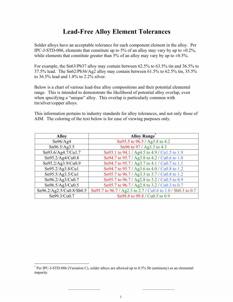
Lead-Free Alloy Element Tolerances
Solder alloys have an acceptable tolerance for each component element in the alloy. Per IPC-J-STD-006, elements that constitute up to 5% of an alloy may vary by up to ±0.2%, while elements that constitute greater than 5% of an alloy may vary by up to ±0.5%. For example, the Sn63/Pb37 alloy may contain between 62.5% to 63.5% tin and 36.5% to 37.5% lead. The Sn62/Pb36/Ag2 alloy may contain between 61.5% to 62.5% tin, 35.5% to 36.5% lead and 1.8% to 2.2% silver. Below is a chart of various lead-free alloy compositions and their potential elemental range. This is intended to demonstrate the likelihood of potential alloy overlap, even when specifying a �unique� alloy. This overlap is particularly common with tin/silver/copper alloys. This information pertains to industry standards for alloy tolerances, and not only those of AIM. The coloring of the text below is for ease of viewing purposes only.
Alloy Alloy Range* Sn96/Ag4 Sn95.5 to 96.5 / Ag3.8 to 4.2
Sn96.5/Ag3.5 Sn96 to 97 / Ag3.3 to 4.3 Sn93.6/Ag4.7/Cu1.7 Sn93.1 to 94.1 / Ag4.5 to 4.9 / Cu1.5 to 1.9 Sn95.2/Ag4/Cu0.8 Sn94.7 to 95.7 / Ag3.8 to 4.2 / Cu0.6 to 1.0
Sn95.2/Ag3.9/Cu0.9 Sn94.7 to 95.7 / Ag3.7 to 4.1 / Cu0.7 to 1.1 Sn95.2/Ag3.8/Cu1 Sn94.7 to 95.7 / Ag3.6 to 4.0 / Cu0.8 to 1.2 Sn95.5/Ag3.5/Cu1 Sn95.7 to 96.7 / Ag3.3 to 3.7 / Cu0.8 to 1.2 Sn96.2/Ag3/Cu0.7 Sn95.7 to 96.7 / Ag2.8 to 3.2 / Cu0.5 to 0.9 Sn96.5/Ag3/Cu0.5 Sn95.7 to 96.7 / Ag2.8 to 3.2 / Cu0.3 to 0.7
Sn96.2/Ag2.5/Cu0.8/Sb0.5 Sn95.7 to 96.7 / Ag2.3 to 2.7 / Cu0.6 to 1.0 / Sb0.3 to 0.7 Sn99.3/Cu0.7 Sn98.8 to 99.8 / Cu0.5 to 0.9
* Per IPC-J-STD-006 (Variation C), solder alloys are allowed up to 0.5% Sb (antimony) as an elemental impurity
5
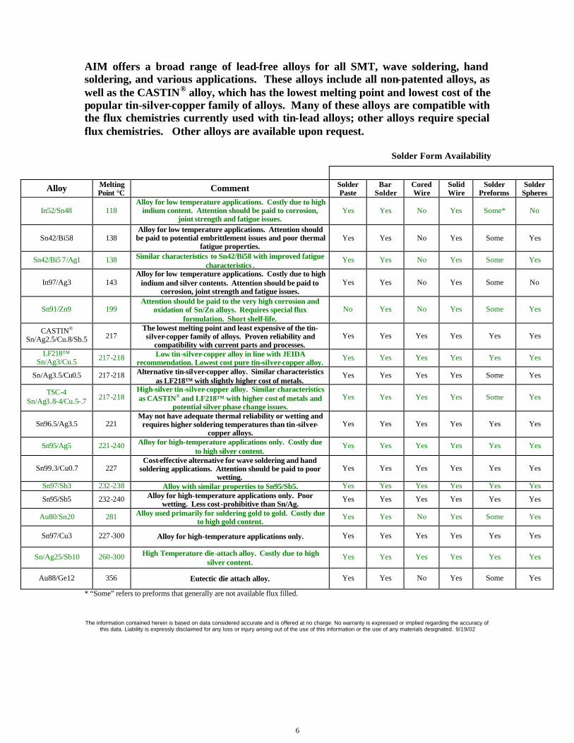
AIM offers a broad range of lead-free alloys for all SMT, wave soldering, hand soldering, and various applications. These alloys include all non-patented alloys, as well as the CASTIN® alloy, which has the lowest melting point and lowest cost of the popular tin-silver-copper family of alloys. Many of these alloys are compatible with the flux chemistries currently used with tin-lead alloys; other alloys require special flux chemistries. Other alloys are available upon request.
Solder Form Availability
Alloy Melting Point °C Comment Solder
Paste Bar
Solder Cored Wire
Solid Wire
Solder Preforms
Solder Spheres
In52/Sn48 118 Alloy for low temperature applications. Costly due to high
indium content. Attention should be paid to corrosion, joint strength and fatigue issues.
Yes Yes No Yes Some* No
Sn42/Bi58 138 Alloy for low temperature applications. Attention should
be paid to potential embrittlement issues and poor thermal fatigue properties.
Yes Yes No Yes Some Yes
Sn42/Bi5 7/Ag1 138 Similar characteristics to Sn42/Bi58 with improved fatigue characteristics .
Yes Yes No Yes Some Yes
In97/Ag3 143 Alloy for low temperature applications. Costly due to high
indium and silver contents. Attention should be paid to corrosion, joint strength and fatigue issues.
Yes Yes No Yes Some No
Sn91/Zn9 199 Attention should be paid to the very high corrosion and
oxidation of Sn/Zn alloys. Requires special flux formulation. Short shelf-life.
No Yes No Yes Some Yes
CASTIN®
Sn/Ag2.5/Cu.8/Sb.5 217 The lowest melting point and least expensive of the tin-silver-copper family of alloys. Proven reliability and
compatibility with current parts and processes. Yes Yes Yes Yes Yes Yes
LF218™ Sn/Ag3/Cu.5 217-218 Low tin-silver-copper alloy in line with JEIDA
recommendation. Lowest cost pure tin-silver-copper alloy. Yes Yes Yes Yes Yes Yes
Sn/Ag3.5/Cu0.5 217-218 Alternative tin-silver-copper alloy. Similar characteristics as LF218™ with slightly higher cost of metals.
Yes Yes Yes Yes Some Yes
TSC-4 Sn/Ag3.8-4/Cu.5-.7 217-218
High-silver tin-silver-copper alloy. Similar characteristics as CASTIN® and LF218™ with higher cost of metals and
potential silver phase change issues. Yes Yes Yes Yes Some Yes
Sn96.5/Ag3.5 221 May not have adequate thermal reliability or wetting and
requires higher soldering temperatures than tin-silver-copper alloys.
Yes Yes Yes Yes Yes Yes
Sn95/Ag5 221-240 Alloy for high-temperature applications only. Costly due to high silver content.
Yes Yes Yes Yes Yes Yes
Sn99.3/Cu0.7 227 Cost-effective alternative for wave soldering and hand
soldering applications. Attention should be paid to poor wetting.
Yes Yes Yes Yes Yes Yes
Sn97/Sb3 232-238 Alloy with similar properties to Sn95/Sb5. Yes Yes Yes Yes Yes Yes
Sn95/Sb5 232-240 Alloy for high-temperature applications only. Poor wetting. Less cost-prohibitive than Sn/Ag.
Yes Yes Yes Yes Yes Yes
Au80/Sn20 281 Alloy used primarily for soldering gold to gold. Costly due to high gold content.
Yes Yes No Yes Some Yes
Sn97/Cu3 227-300 Alloy for high-temperature applications only. Yes Yes Yes Yes Yes Yes
Sn/Ag25/Sb10 260-300 High Temperature die-attach alloy. Costly due to high silver content.
Yes Yes Yes Yes Yes Yes
Au88/Ge12 356 Eutectic die attach alloy. Yes Yes No Yes Some Yes
* “Some” refers to preforms that generally are not available flux filled.
The information contained herein is based on data considered accurate and is offered at no charge. No warranty is expressed or implied regarding the accuracy of this data. Liability is expressly disclaimed for any loss or injury arising out of the use of this information or the use of any materials designated. 9/19/02
-800-CALL-AIM, fax 401-463-0203, or visit us on the web at www.leadfree.com or www.aimsolder.com
6
AIM Lead-Free Assembly Products AIM has been developing lead-free alloys and researching the subject of lead-free soldering since the 1980s, and we have a great deal of knowledge on lead-free alloys, processes, and the issue in general. We would be happy to work with your company on the implementation of a lead-free process and to share the vast data and experience on lead-free alloys that AIM has accumulated over the years. Please feel free to contact AIM at anytime so that we may be of assistance during this often-complicated transition period.
AIM Lead-Free Assembly Products AIM has lead-free no clean, water soluble and rosin solder pastes, lead-free bar solders and compatible fluxes, and lead-free cored wire, solid wire, performs and spheres.
Lead-Free Solder Pastes AIM�s lead-free solder pastes are available in a variety of chemistries, alloys (see chart on back page), powder mesh size, and packaging and offer the following features:
• Excellent printability and tack force • Long tack time and stencil life • Excellent wetting and solderability • Low residues • Easily cleaned residues • Pass Bellcore and IPC reliability testing
In addition, specific formulas may be requested that offer the following advantages:
• Easily pin probe tested • High heat and humidity resistance • Suitable for high-speed printing • Residues safe to be left uncleaned on
RF devices up to 50 gigahertz • Eliminate solder defects such as voiding
and solder beading
Lead-Free Bar Solder AIM�s lead-free bar solder is available in a variety of alloys (see chart on back page), cast (1Kg), extruded (1lb), or margash (10lb) and are manufactured in two different grades:
• Electropure Grade- Very low impurities; Ultra low drossing.
• IPC Grade- Lower cost, Meets IPC-J-STD-006 specifications.
Lead-Free Compatible Liquid Fluxes AIM�s lead-free compatible liquid fluxes are available in a variety of chemistries and packaging and offer the following features:
• Available VOC-Free and alcohol-based • Ultra-low residues • Excellent wetting and solderability • May be sprayed, foamed, dipped, or
brushed • Pass Bellcore and IPC reliability testing
Lead-Free Cored and Solid Wire Solder AIM�s lead-free wire solders are available in a variety of alloys (see chart on back page), diameters, spool sizes, and solid or cored in a variety of chemistries and offer the following features:
• Low fuming and low odor • Excellent wetting and solderability • Low Residue • Guaranteed void-free core • Pass Bellcore and IPC reliability testing
Lead-Free Preforms and Spheres
AIM�s lead-free performs and spheres are available in a variety of alloys (see chart on back page), some flux filled or coated, and the following shapes.
• Spheres • Segments • Discs • Horseshoes • Rings • Washers • Other specialty shapes and sizes as
requested
No matter what the application, AIM has the lead-free products and process knowledge required to help your company in the transition to lead-free soldering in the most logical and economical ways possible.
7
Lead-Free Consultation Services
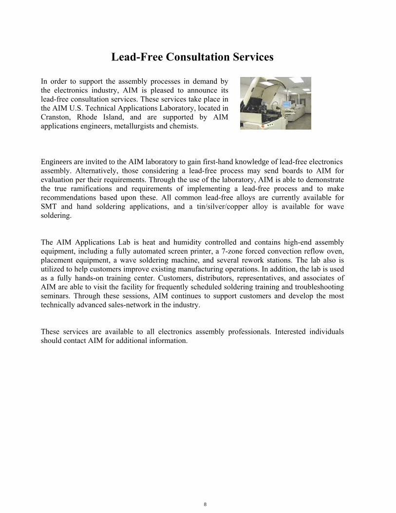
In order to support the assembly processes in demand by the electronics industry, AIM is pleased to announce its lead-free consultation services. These services take place in the AIM U.S. Technical Applications Laboratory, located in Cranston, Rhode Island, and are supported by AIM applications engineers, metallurgists and chemists. Engineers are invited to the AIM laboratory to gain first-hand knowledge of lead-free electronics assembly. Alternatively, those considering a lead-free process may send boards to AIM for evaluation per their requirements. Through the use of the laboratory, AIM is able to demonstrate the true ramifications and requirements of implementing a lead-free process and to make recommendations based upon these. All common lead-free alloys are currently available for SMT and hand soldering applications, and a tin/silver/copper alloy is available for wave soldering. The AIM Applications Lab is heat and humidity controlled and contains high-end assembly equipment, including a fully automated screen printer, a 7-zone forced convection reflow oven, placement equipment, a wave soldering machine, and several rework stations. The lab also is utilized to help customers improve existing manufacturing operations. In addition, the lab is used as a fully hands-on training center. Customers, distributors, representatives, and associates of AIM are able to visit the facility for frequently scheduled soldering training and troubleshooting seminars. Through these sessions, AIM continues to support customers and develop the most technically advanced sales-network in the industry. These services are available to all electronics assembly professionals. Interested individuals should contact AIM for additional information.
8
A COMPARISON OF TIN-SILVER-COPPER LEAD-FREE SOLDER ALLOYS
Karl Seelig and David Suraski/AIM [email protected]
May 2003 ABSTRACT As the electronics industry begins to focus upon the tin-silver-copper family of alloys as a viable replacement for tin-lead solders, research needs to be done to determine if any particular alloy is best suited for the broadest range of applications. The tin-silver-copper family of alloys has earned a great deal of positive response from various industry consortia and organizations in recent years and the majority of manufacturers plan on implementing one of these alloys. However, as there are several different alloy formulations within the tin-silver-copper family, background information is necessary to determine which alloy is best suited for the broadest range of applications. Keywords: Lead-Free, Alloys, Tin-Silver-Copper, Comparison, Cost, Availability, Patents, Printing, Melting Points, Wetting, Reliability. 1. INTRODUCTION It is inevitable that lead will be eliminated from a great deal of electronics assembly. Whether this will be the result of legislation, marketing pressure, or de facto trade-barriers is not important. The only important aspect of this issue anymore is that it is real, and that it is coming within the next few years. Therefore, electronics manufacturers need to be cognizant of the solder alloy choices available to them, and the fact that not all alloys, including those within the same families, share the same characteristics. Based on recent industry-wide developments, it appears that the choice of candidate lead-free alloys to replace tin-lead for electronics assembly is narrowing. Despite a confusing patent situation and continuing questions about reliability, the tin-silver-copper family of alloys has earned a great deal of positive response from various industry consortia and organizations in recent years and the majority of manufacturers plan on implementing one of these alloys.i In general, this family of alloys demonstrates relatively low melting points, good reliability characteristics, and, depending upon the exact composition, reasonable cost. However, as there are several different alloy formulations within the tin-silver-copper family, background information is necessary to determine which alloy is best suited for the broadest range of applications. It also should be noted that these (sometimes nominal) varying alloy compositions are confusing to the industry and create an inventory nightmare for solder manufacturers and end-users. The result is a higher cost for the industry. Selecting a “default” lead-free alloy benefits the entire supply chain. This is especially true of EMS providers, who may be forced to stock multiple alloys based upon the requirements of their customers. 2. TIN-SILVER-COPPER ALLOY COMPARISON The alloys tested are the most promising and popular of the tin-silver-copper alloys: Sn96.5/Ag3.0/Cu0.5, Sn95.5/Ag3.8/Cu0.7, and Sn95.5/Ag4.0/Cu0.5. In addition the Sn96.2/Ag2.5/Cu0.8/Sb0.5 alloy is used in some cases as a low-silver content alternative for comparative purposes. This paper is meant to provide the baseline information for these alloys needed to fairly compare one to another. Objective test methodologies were used to represent
9
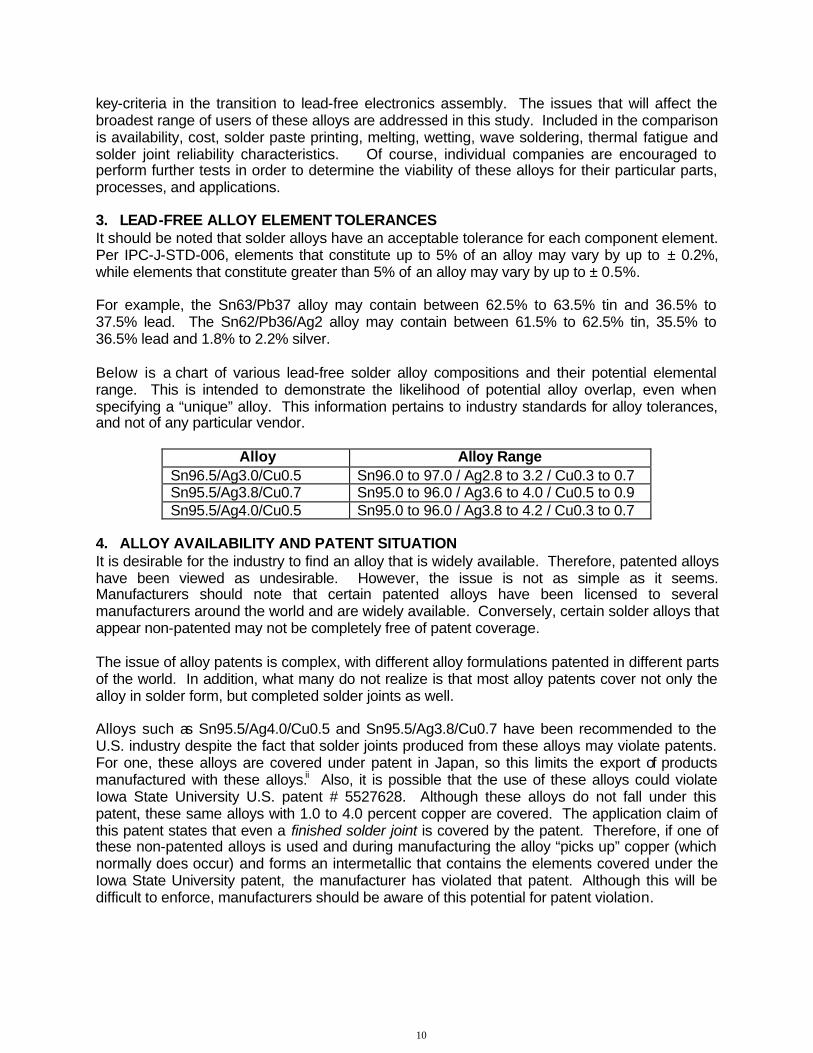
key-criteria in the transition to lead-free electronics assembly. The issues that will affect the broadest range of users of these alloys are addressed in this study. Included in the comparison is availability, cost, solder paste printing, melting, wetting, wave soldering, thermal fatigue and solder joint reliability characteristics. Of course, individual companies are encouraged to perform further tests in order to determine the viability of these alloys for their particular parts, processes, and applications. 3. LEAD-FREE ALLOY ELEMENT TOLERANCES It should be noted that solder alloys have an acceptable tolerance for each component element. Per IPC-J-STD-006, elements that constitute up to 5% of an alloy may vary by up to ± 0.2%, while elements that constitute greater than 5% of an alloy may vary by up to ± 0.5%. For example, the Sn63/Pb37 alloy may contain between 62.5% to 63.5% tin and 36.5% to 37.5% lead. The Sn62/Pb36/Ag2 alloy may contain between 61.5% to 62.5% tin, 35.5% to 36.5% lead and 1.8% to 2.2% silver. Below is a chart of various lead-free solder alloy compositions and their potential elemental range. This is intended to demonstrate the likelihood of potential alloy overlap, even when specifying a “unique” alloy. This information pertains to industry standards for alloy tolerances, and not of any particular vendor.
Alloy Alloy Range Sn96.5/Ag3.0/Cu0.5 Sn96.0 to 97.0 / Ag2.8 to 3.2 / Cu0.3 to 0.7 Sn95.5/Ag3.8/Cu0.7 Sn95.0 to 96.0 / Ag3.6 to 4.0 / Cu0.5 to 0.9 Sn95.5/Ag4.0/Cu0.5 Sn95.0 to 96.0 / Ag3.8 to 4.2 / Cu0.3 to 0.7
4. ALLOY AVAILABILITY AND PATENT SITUATION It is desirable for the industry to find an alloy that is widely available. Therefore, patented alloys have been viewed as undesirable. However, the issue is not as simple as it seems. Manufacturers should note that certain patented alloys have been licensed to several manufacturers around the world and are widely available. Conversely, certain solder alloys that appear non-patented may not be completely free of patent coverage. The issue of alloy patents is complex, with different alloy formulations patented in different parts of the world. In addition, what many do not realize is that most alloy patents cover not only the alloy in solder form, but completed solder joints as well. Alloys such as Sn95.5/Ag4.0/Cu0.5 and Sn95.5/Ag3.8/Cu0.7 have been recommended to the U.S. industry despite the fact that solder joints produced from these alloys may violate patents. For one, these alloys are covered under patent in Japan, so this limits the export of products manufactured with these alloys.ii Also, it is possible that the use of these alloys could violate Iowa State University U.S. patent # 5527628. Although these alloys do not fall under this patent, these same alloys with 1.0 to 4.0 percent copper are covered. The application claim of this patent states that even a finished solder joint is covered by the patent. Therefore, if one of these non-patented alloys is used and during manufacturing the alloy “picks up” copper (which normally does occur) and forms an intermetallic that contains the elements covered under the Iowa State University patent, the manufacturer has violated that patent. Although this will be difficult to enforce, manufacturers should be aware of this potential for patent violation.
10
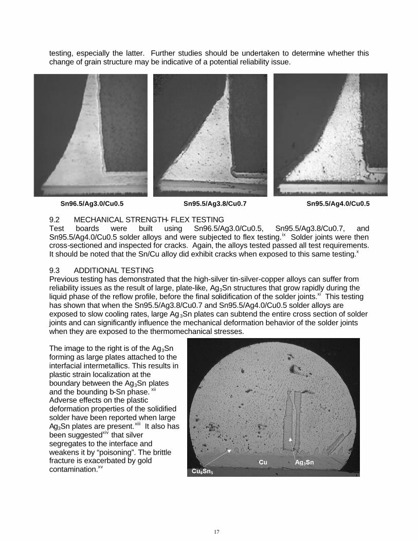
Sn96.5/Ag3.0/Cu0.5
Sn95.5/Ag3.8/Cu0.7
Sn95.5/Ag4.0/Cu0.5
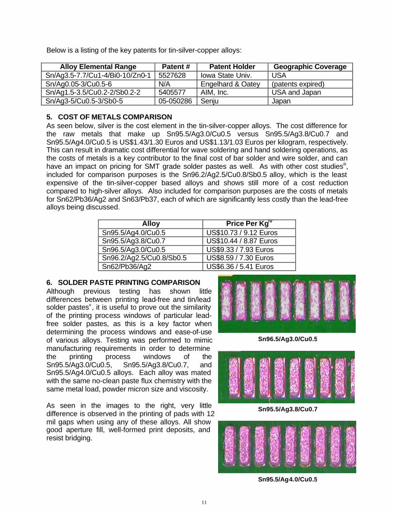
Below is a listing of the key patents for tin-silver-copper alloys:
Alloy Elemental Range Patent # Patent Holder Geographic Coverage Sn/Ag3.5-7.7/Cu1-4/Bi0-10/Zn0-1 5527628 Iowa State Univ. USA Sn/Ag0.05-3/Cu0.5-6 N/A Engelhard & Oatey (patents expired) Sn/Ag1.5-3.5/Cu0.2-2/Sb0.2-2 5405577 AIM, Inc. USA and Japan Sn/Ag3-5/Cu0.5-3/Sb0-5 05-050286 Senju Japan 5. COST OF METALS COMPARISON As seen below, silver is the cost element in the tin-silver-copper alloys. The cost difference for the raw metals that make up Sn95.5/Ag3.0/Cu0.5 versus Sn95.5/Ag3.8/Cu0.7 and Sn95.5/Ag4.0/Cu0.5 is US$1.43/1.30 Euros and US$1.13/1.03 Euros per kilogram, respectively. This can result in dramatic cost differential for wave soldering and hand soldering operations, as the costs of metals is a key contributor to the final cost of bar solder and wire solder, and can have an impact on pricing for SMT grade solder pastes as well. As with other cost studiesiii, included for comparison purposes is the Sn96.2/Ag2.5/Cu0.8/Sb0.5 alloy, which is the least expensive of the tin-silver-copper based alloys and shows still more of a cost reduction compared to high-silver alloys. Also included for comparison purposes are the costs of metals for Sn62/Pb36/Ag2 and Sn63/Pb37, each of which are significantly less costly than the lead-free alloys being discussed.
Alloy Price Per Kgiv Sn95.5/Ag4.0/Cu0.5 US$10.73 / 9.12 Euros Sn95.5/Ag3.8/Cu0.7 US$10.44 / 8.87 Euros Sn96.5/Ag3.0/Cu0.5 US$9.33 / 7.93 Euros Sn96.2/Ag2.5/Cu0.8/Sb0.5 US$8.59 / 7.30 Euros Sn62/Pb36/Ag2 US$6.36 / 5.41 Euros
6. SOLDER PASTE PRINTING COMPARISON Although previous testing has shown little differences between printing lead-free and tin/lead solder pastesv , it is useful to prove out the similarity of the printing process windows of particular lead-free solder pastes, as this is a key factor when determining the process windows and ease-of-use of various alloys. Testing was performed to mimic manufacturing requirements in order to determine the printing process windows of the Sn95.5/Ag3.0/Cu0.5, Sn95.5/Ag3.8/Cu0.7, and Sn95.5/Ag4.0/Cu0.5 alloys. Each alloy was mated with the same no-clean paste flux chemistry with the same metal load, powder micron size and viscosity. As seen in the images to the right, very little difference is observed in the printing of pads with 12 mil gaps when using any of these alloys. All show good aperture fill, well-formed print deposits, and resist bridging.
11
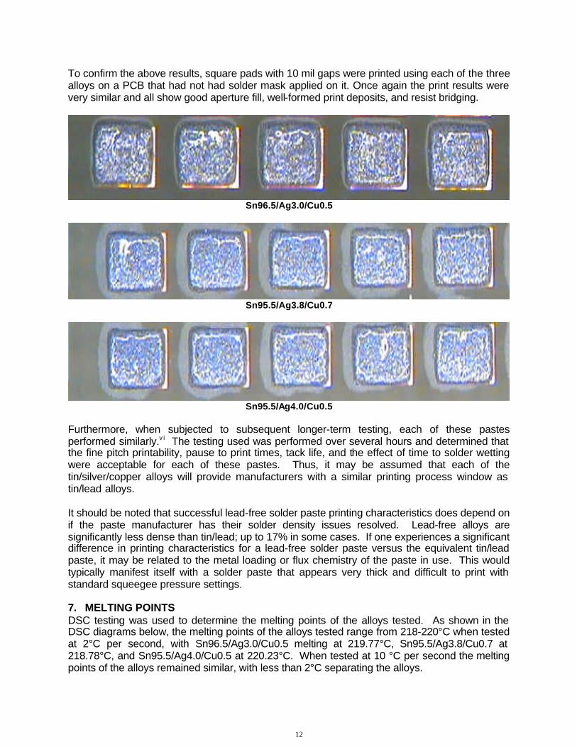
To confirm the above results, square pads with 10 mil gaps were printed using each of the three alloys on a PCB that had not had solder mask applied on it. Once again the print results were very similar and all show good aperture fill, well-formed print deposits, and resist bridging.
Sn96.5/Ag3.0/Cu0.5
Sn95.5/Ag3.8/Cu0.7
Sn95.5/Ag4.0/Cu0.5
Furthermore, when subjected to subsequent longer-term testing, each of these pastes performed similarly.v i The testing used was performed over several hours and determined that the fine pitch printability, pause to print times, tack life, and the effect of time to solder wetting were acceptable for each of these pastes. Thus, it may be assumed that each of the tin/silver/copper alloys will provide manufacturers with a similar printing process window as tin/lead alloys. It should be noted that successful lead-free solder paste printing characteristics does depend on if the paste manufacturer has their solder density issues resolved. Lead-free alloys are significantly less dense than tin/lead; up to 17% in some cases. If one experiences a significant difference in printing characteristics for a lead-free solder paste versus the equivalent tin/lead paste, it may be related to the metal loading or flux chemistry of the paste in use. This would typically manifest itself with a solder paste that appears very thick and difficult to print with standard squeegee pressure settings. 7. MELTING POINTS DSC testing was used to determine the melting points of the alloys tested. As shown in the DSC diagrams below, the melting points of the alloys tested range from 218-220°C when tested at 2°C per second, with Sn96.5/Ag3.0/Cu0.5 melting at 219.77°C, Sn95.5/Ag3.8/Cu0.7 at 218.78°C, and Sn95.5/Ag4.0/Cu0.5 at 220.23°C. When tested at 10 °C per second the melting points of the alloys remained similar, with less than 2°C separating the alloys.
12
Sn96.5/Ag3.0/Cu0.5 Sn95.5/Ag3.8/Cu0.7 Sn95.5/Ag4.0/Cu0.5
Sn96.5/Ag3.0/Cu0.5 Sn95.5/Ag3.8/Cu0.7 Sn95.5/Ag4.0/Cu0.5
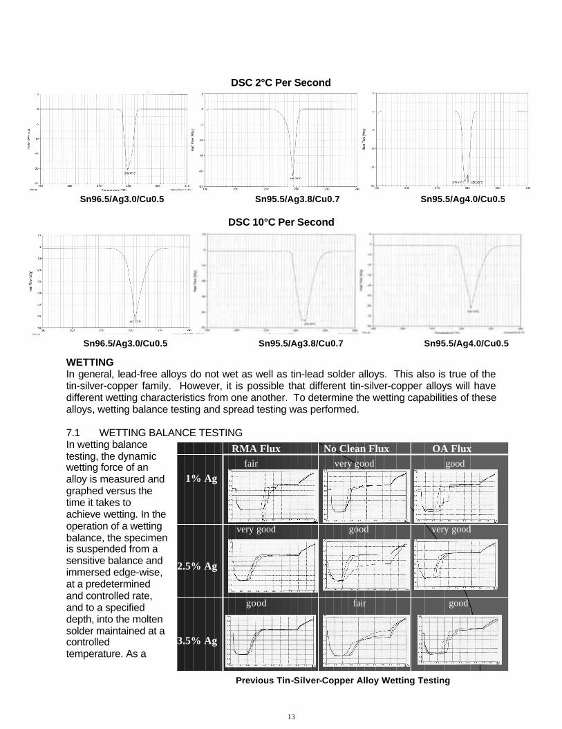
RMA Flux No Clean Flux OA Fluxfair very good good
1% Ag
very good good very good
2.5% Ag
good fair good
3.5% Ag
Previous Tin-Silver-Copper Alloy Wetting Testing
DSC 2°C Per Second
DSC 10°C Per Second
WETTING In general, lead-free alloys do not wet as well as tin-lead solder alloys. This also is true of the tin-silver-copper family. However, it is possible that different tin-silver-copper alloys will have different wetting characteristics from one another. To determine the wetting capabilities of these alloys, wetting balance testing and spread testing was performed.
7.1 WETTING BALANCE TESTING In wetting balance testing, the dynamic wetting force of an alloy is measured and graphed versus the time it takes to achieve wetting. In the operation of a wetting balance, the specimen is suspended from a sensitive balance and immersed edge-wise, at a predetermined and controlled rate, and to a specified depth, into the molten solder maintained at a controlled temperature. As a
13
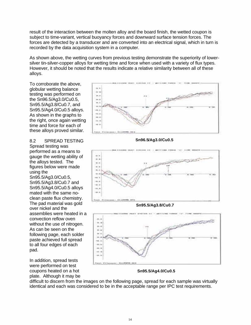
Sn95.5/Ag3.8/Cu0.7
Sn95.5/Ag4.0/Cu0.5
Sn96.5/Ag3.0/Cu0.5
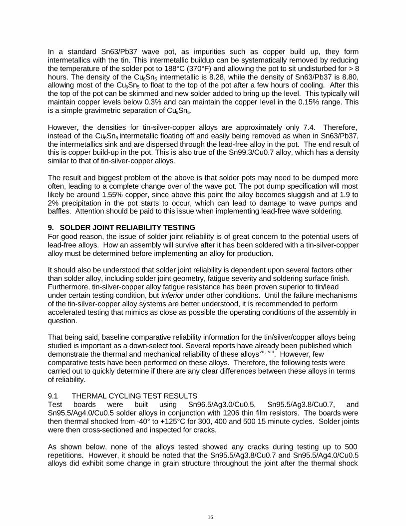
result of the interaction between the molten alloy and the board finish, the wetted coupon is subject to time-variant, vertical buoyancy forces and downward surface tension forces. The forces are detected by a transducer and are converted into an electrical signal, which in turn is recorded by the data acquisition system in a computer. As shown above, the wetting curves from previous testing demonstrate the superiority of lower-silver tin-silver-copper alloys for wetting time and force when used with a variety of flux types. However, it should be noted that the results indicate a relative similarity between all of these alloys. To corroborate the above, globular wetting balance testing was performed on the Sn96.5/Ag3.0/Cu0.5, Sn95.5/Ag3.8/Cu0.7, and Sn95.5/Ag4.0/Cu0.5 alloys. As shown in the graphs to the right, once again wetting time and force for each of these alloys proved similar. 8.2 SPREAD TESTING Spread testing was performed as a means to gauge the wetting ability of the alloys tested. The figures below were made using the Sn95.5/Ag3.0/Cu0.5, Sn95.5/Ag3.8/Cu0.7 and Sn95.5/Ag4.0/Cu0.5 alloys mated with the same no-clean paste flux chemistry. The pad material was gold over nickel and the assemblies were heated in a convection reflow oven without the use of nitrogen. As can be seen on the following page, each solder paste achieved full spread to all four edges of each pad. In addition, spread tests were performed on test coupons heated on a hot plate. Although it may be difficult to discern from the images on the following page, spread for each sample was virtually identical and each was considered to be in the acceptable range per IPC test requirements.
14
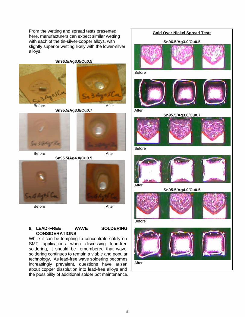
Sn96.5/Ag3.0/Cu0.5
Before After
Sn95.5/Ag3.8/Cu0.7
Before After
Sn95.5/Ag4.0/Cu0.5
Before After
Gold Over Nickel Spread Tests
Sn96.5/Ag3.0/Cu0.5
Before
After Sn95.5/Ag3.8/Cu0.7
Before
After Sn95.5/Ag4.0/Cu0.5
Before
After
From the wetting and spread tests presented here, manufacturers can expect similar wetting with each of the tin-silver-copper alloys, with slightly superior wetting likely with the lower-silver alloys.
8. LEAD-FREE WAVE SOLDERING
CONSIDERATIONS While it can be tempting to concentrate solely on SMT applications when discussing lead-free soldering, it should be remembered that wave soldering continues to remain a viable and popular technology. As lead-free wave soldering becomes increasingly prevalent, questions have arisen about copper dissolution into lead-free alloys and the possibility of additional solder pot maintenance.
15
In a standard Sn63/Pb37 wave pot, as impurities such as copper build up, they form intermetallics with the tin. This intermetallic buildup can be systematically removed by reducing the temperature of the solder pot to 188°C (370°F) and allowing the pot to sit undisturbed for > 8 hours. The density of the Cu6Sn5 intermetallic is 8.28, while the density of Sn63/Pb37 is 8.80, allowing most of the Cu6Sn5 to float to the top of the pot after a few hours of cooling. After this the top of the pot can be skimmed and new solder added to bring up the level. This typically will maintain copper levels below 0.3% and can maintain the copper level in the 0.15% range. This is a simple gravimetric separation of Cu6Sn5. However, the densities for tin-silver-copper alloys are approximately only 7.4. Therefore, instead of the Cu6Sn5 intermetallic floating off and easily being removed as when in Sn63/Pb37, the intermetallics sink and are dispersed through the lead-free alloy in the pot. The end result of this is copper build-up in the pot. This is also true of the Sn99.3/Cu0.7 alloy, which has a density similar to that of tin-silver-copper alloys. The result and biggest problem of the above is that solder pots may need to be dumped more often, leading to a complete change over of the wave pot. The pot dump specification will most likely be around 1.55% copper, since above this point the alloy becomes sluggish and at 1.9 to 2% precipitation in the pot starts to occur, which can lead to damage to wave pumps and baffles. Attention should be paid to this issue when implementing lead-free wave soldering. 9. SOLDER JOINT RELIABILITY TESTING For good reason, the issue of solder joint reliability is of great concern to the potential users of lead-free alloys. How an assembly will survive after it has been soldered with a tin-silver-copper alloy must be determined before implementing an alloy for production. It should also be understood that solder joint reliability is dependent upon several factors other than solder alloy, including solder joint geometry, fatigue severity and soldering surface finish. Furthermore, tin-silver-copper alloy fatigue resistance has been proven superior to tin/lead under certain testing condition, but inferior under other conditions. Until the failure mechanisms of the tin-silver-copper alloy systems are better understood, it is recommended to perform accelerated testing that mimics as close as possible the operating conditions of the assembly in question. That being said, baseline comparative reliability information for the tin/silver/copper alloys being studied is important as a down-select tool. Several reports have already been published which demonstrate the thermal and mechanical reliability of these alloysvii, viii. However, few comparative tests have been performed on these alloys. Therefore, the following tests were carried out to quickly determine if there are any clear differences between these alloys in terms of reliability. 9.1 THERMAL CYCLING TEST RESULTS Test boards were built using Sn96.5/Ag3.0/Cu0.5, Sn95.5/Ag3.8/Cu0.7, and Sn95.5/Ag4.0/Cu0.5 solder alloys in conjunction with 1206 thin film resistors. The boards were then thermal shocked from -40° to +125°C for 300, 400 and 500 15 minute cycles. Solder joints were then cross-sectioned and inspected for cracks. As shown below, none of the alloys tested showed any cracks during testing up to 500 repetitions. However, it should be noted that the Sn95.5/Ag3.8/Cu0.7 and Sn95.5/Ag4.0/Cu0.5 alloys did exhibit some change in grain structure throughout the joint after the thermal shock
16
Sn96.5/Ag3.0/Cu0.5 Sn95.5/Ag3.8/Cu0.7 Sn95.5/Ag4.0/Cu0.5
testing, especially the latter. Further studies should be undertaken to determine whether this change of grain structure may be indicative of a potential reliability issue.
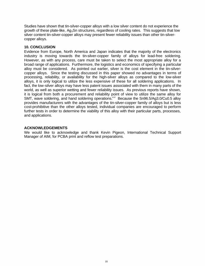
9.2 MECHANICAL STRENGTH- FLEX TESTING Test boards were built using Sn96.5/Ag3.0/Cu0.5, Sn95.5/Ag3.8/Cu0.7, and Sn95.5/Ag4.0/Cu0.5 solder alloys and were subjected to flex testing. ix Solder joints were then cross-sectioned and inspected for cracks. Again, the alloys tested passed all test requirements. It should be noted that the Sn/Cu alloy did exhibit cracks when exposed to this same testing.x 9.3 ADDITIONAL TESTING Previous testing has demonstrated that the high-silver tin-silver-copper alloys can suffer from reliability issues as the result of large, plate-like, Ag3Sn structures that grow rapidly during the liquid phase of the reflow profile, before the final solidification of the solder joints.xi This testing has shown that when the Sn95.5/Ag3.8/Cu0.7 and Sn95.5/Ag4.0/Cu0.5 solder alloys are exposed to slow cooling rates, large Ag 3Sn plates can subtend the entire cross section of solder joints and can significantly influence the mechanical deformation behavior of the solder joints when they are exposed to the thermomechanical stresses. The image to the right is of the Ag3Sn forming as large plates attached to the interfacial intermetallics. This results in plastic strain localization at the boundary between the Ag3Sn plates and the bounding b-Sn phase. xii Adverse effects on the plastic deformation properties of the solidified solder have been reported when large Ag3Sn plates are present.xiii It also has been suggestedxiv that silver segregates to the interface and weakens it by “poisoning”. The brittle fracture is exacerbated by gold contamination.xv
17
Studies have shown that tin-silver-copper alloys with a low silver content do not experience the growth of these plate-like, Ag3Sn structures, regardless of cooling rates. This suggests that low silver content tin-silver-copper alloys may present fewer reliability issues than other tin-silver-copper alloys. 10. CONCLUSION Evidence from Europe, North America and Japan indicates that the majority of the electronics industry is moving towards the tin-silver-copper family of alloys for lead-free soldering. However, as with any process, care must be taken to select the most appropriate alloy for a broad range of applications. Furthermore, the logistics and economics of specifying a particular alloy must be considered. As pointed out earlier, silver is the cost element in the tin-silver-copper alloys. Since the testing discussed in this paper showed no advantages in terms of processing, reliability, or availability for the high-silver alloys as compared to the low-silver alloys, it is only logical to utilize the less expensive of these for all soldering applications. In fact, the low-silver alloys may have less patent issues associated with them in many parts of the world, as well as superior wetting and fewer reliability issues. As previous reports have shown, it is logical from both a procurement and reliability point of view to utilize the same alloy for SMT, wave soldering, and hand soldering operations.xv i Because the Sn96.5/Ag3.0/Cu0.5 alloy provides manufacturers with the advantages of the tin-silver-copper family of alloys but is less cost-prohibitive than the other alloys tested, individual companies are encouraged to perform further tests in order to determine the viability of this alloy with their particular parts, processes, and applications. ACKNOWLEDGEMENTS We would like to acknowledge and thank Kevin Pigeon, International Technical Support Manager of AIM, for PCBA print and reflow test preparations.
18
REFERENCES i Nimmo, Kay, SOLDERTEC at Tin Technology Ltd. “Second European Lead-Free Soldering Technology Roadmap (February 2003) and Framework for an International Lead-Free Soldering Roadmap (December 2002)”. ii Senju Corporation patent # 3027441. iii Lee, Ning-Cheng, “Lead-Free Soldering- Where the World is Going”. Advanced Microelectronics, pp. 29-34, September/October 1999. 6 Based upon published cost of metals and US$/Euro exchange rate of June 5, 2003 v Whiteman, Lee. “Issues And Solutions To Implementing Lead Free Soldering”. May 2000. v i Testing performed was the AIM 24 Hour - 15 Board Challenge. Contact the author for a full description of the test procedure. vii Sohn, John. "Are Lead-Free Solder Joints Reliable?" Circuits Assembly, June 2002, p. 31. viii Kariya, Yoshiharu and Plumbridge, William. “Mechanical Properties of Sn-3.0mass%Ag-0.5mass%Cu Alloy”. Materials Engineering Department, The Open University, UK. ix Contact the author for test procedures. x Seelig, Karl and Suraski, David. ”Advanced Material and Process Issues Lead-Free Electronics Assembly”. April 2001. xi Henderson, Donald et al. “Ag3Sn Plate Formation in the Solidification of Near Ternary Eutectic Sn-Ag-Cu Alloys”. xii D. R. Frear, J. W. Jang, J. K. Lin and C. Zhang. “Pb-Free Solders for Flip-Chip Interconnects”. JOM, vol.53, No.6 ( June 2001). xiii K. S. Kim, S. H. Huh and K. Suganuma, "Effects of Cooling Speed on Microstructure and Tensile Properties of Sn-Ag-Cu Alloys". Osaka University, Japan.. August 2002. xiv D.R. Frear and P.T. Vianco, “Intermetallic Growth Behavior of Low and High Melting Temperature Solder Alloys,” Metall. Trans. A, 25A (1994), pp. 1509–1523. xv M. Harada and R. Satoh, “Mechanical Characteristics of 96.5 Sn/ 3.5 Ag Solder in Micro-bonding,” IEEE Trans. on Comp, Hybrids, and Manuf. Tech., 13 (4) (1990), pp. 736–742. xv i Seelig, Karl and Suraski, David. “Finally! Practical Guidelines for Achieving Successful Lead-Free Assembly”. APEX 2003 proceedings.
19
PWBs alloy flux handling
printing reflow wave rework cleaning inspection
design
purchasing engineering maintenance quality
component
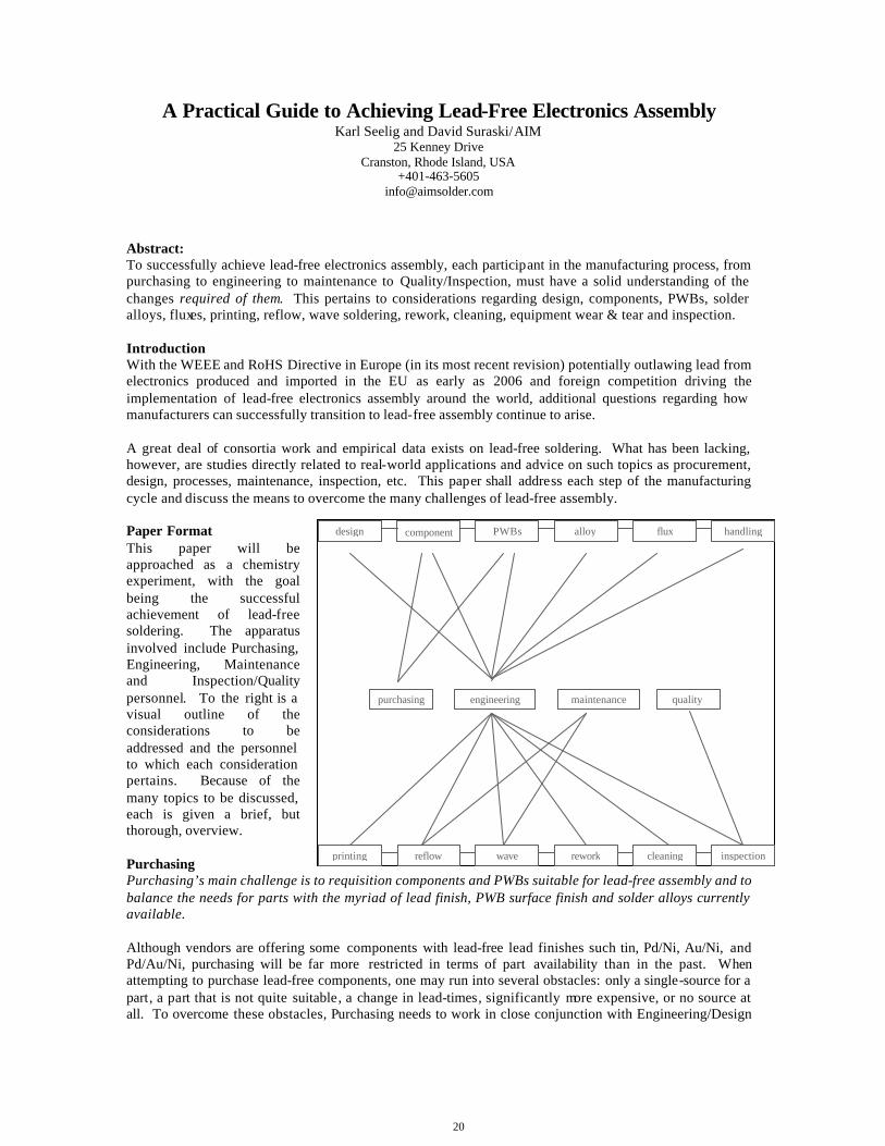
A Practical Guide to Achieving Lead-Free Electronics Assembly Karl Seelig and David Suraski/AIM
25 Kenney Drive Cranston, Rhode Island, USA
+401-463-5605 [email protected]
Abstract: To successfully achieve lead-free electronics assembly, each participant in the manufacturing process, from purchasing to engineering to maintenance to Quality/Inspection, must have a solid understanding of the changes required of them. This pertains to considerations regarding design, components, PWBs, solder alloys, fluxes, printing, reflow, wave soldering, rework, cleaning, equipment wear & tear and inspection. Introduction With the WEEE and RoHS Directive in Europe (in its most recent revision) potentially outlawing lead from electronics produced and imported in the EU as early as 2006 and foreign competition driving the implementation of lead-free electronics assembly around the world, additional questions regarding how manufacturers can successfully transition to lead-free assembly continue to arise. A great deal of consortia work and empirical data exists on lead-free soldering. What has been lacking, however, are studies directly related to real-world applications and advice on such topics as procurement, design, processes, maintenance, inspection, etc. This paper shall address each step of the manufacturing cycle and discuss the means to overcome the many challenges of lead-free assembly. Paper Format This paper will be approached as a chemistry experiment, with the goal being the successful achievement of lead-free soldering. The apparatus involved include Purchasing, Engineering, Maintenance and Inspection/Quality personnel. To the right is a visual outline of the considerations to be addressed and the personnel to which each consideration pertains. Because of the many topics to be discussed, each is given a brief, but thorough, overview. Purchasing Purchasing’s main challenge is to requisition components and PWBs suitable for lead-free assembly and to balance the needs for parts with the myriad of lead finish, PWB surface finish and solder alloys currently available. Although vendors are offering some components with lead-free lead finishes such tin, Pd/Ni, Au/Ni, and Pd/Au/Ni, purchasing will be far more restricted in terms of part availability than in the past. When attempting to purchase lead-free components, one may run into several obstacles: only a single-source for a part, a part that is not quite suitable, a change in lead-times, significantly more expensive, or no source at all. To overcome these obstacles, Purchasing needs to work in close conjunction with Engineering/Design
20
and vendors to ensure that the lead-free parts needed are available and compatible with the manufacturing process. As with components, there is some availability of lead-free PWB surface finishes. OSPs, Au/Ni, Immersion Sn, Ag, and Lead-Free HAL finish PWBs have been on the market for some time now. Again, Purchasing needs to work in close conjunction with Engineering/Design and vendors to ensure that the lead-free parts needed are available compatible with the manufacturing process. Materials Management The many component and PWB coatings, as well as several possible solder alloys results in a huge matrix of potential material intermix, and clearly can complicate materials management. More than ever, purchasing will need to be attuned to which parts go with which product. Once again, Purchasing must work in close conjunction with Engineering to ensure that ordering is streamlined and that the appropriate parts are available for particular jobs. Engineering The switch to lead-free assembly affects virtually all aspects of the Engineering function. Engineering personnel will have to pay close attention to design, components, PWBs, solder alloys, fluxes, and the printing, reflow, wave soldering, rework and cleaning processes and equipment. Design Established PCB-design rules may need to change during the transition to lead-free soldering. Currently, industry guidelines govern component lead-pad and land size, track width and spacing, via and through-hole dimensions, and similar factors to ensure manufacturability and reliability. However, the physical characteristics of any solder include subtle factors, such as its ductility and elasticity. In addition, the local heating of component leads and their pads causes some thermal expansion during operation, which tin-lead solder accommodates and matches. In determining design solutions, Design should try to remain with as many standard parts as possible. This will reduce the unpredictability encountered with atypical parts. In addition, if the assembly is designed to have a long life, factor in the reduced moisture resistance of parts. Furthermore, Design must factor in the higher temperatures required for connectors. Material Considerations The first critical duty is to ensure that the parts to be used will be compatible and reliable for their particular application. Compatibility relates to components , PWBs , solder alloy and flux. Reliability relates to component concerns, which includes such factors as Moisture Sensitivity Level (MSL) Rating, wetting and tin whiskering. Component Reliability Concerns The higher melting temperatures of the lead-free solders that are coming into use mandate components that can withstand the increased temperature stresses of the soldering process. Life -test data for many components at these higher temperatures is less comprehensive than it is for tin/lead processes. To maximize reliability, Engineering should start looking now at all critical components, design rules, fabrication processes, component engineering, and reliability records. A critical factor in the transition to lead-free assembly is the MSL rating of components. To date, industry testing has demonstrated that there is no generic solution for maintaining an IC’s MSL with a higher reflow profile. However, it has been demonstrated that degradation of MSL may increase with increasing profile dwell above 200°C and that MSL typically degrades by one level for every 5 to 10°C increase of peak reflow temperature. Therefore, all ICs must be reclassified for lead-free applications and the impact to MSL. This could result in an increased need to pre-bake parts and more stringent storage methods. As discussed above, several lead-free component lead finishes are available. It should be noted that these different materials have different wetting characteristics and that Engineering should consider wetting when specifying components. Engineering also needs to balance the fact that increased reflow
21
temperatures can improve wetting, but worsen reliability. In addition, Design should be aware of reduced solderability on second-side reflow and through-hole processes. Another hot topic of discussion is tin whiskering, which continues to be an oft-misunderstood and debated subject. Proponents of matte tin argue that whiskering is a result of the plating process, and not necessarily inherent to pure tin. They demonstrate that whiskering can also occur with Sn/Bi, etc. Others, however, suggest that a dopant is needed to offset the whiskering. Engineering should follow the on-going debate and studies regarding this topic, work closely with component vendors and participate in studies to determine the most suitable lead finish for their applications. PWBs Several PWB lead-free surface finish options exist. Many of these, such as OSPs and Au/Ni, have been available for years. Engineering should determine the finish of choice based upon wetting, storage, planarity and cost issues . In addition, it must be ensured that board materials can withstand reflow temperatures without warpage or other damage. For many cases, FR-4 will remain acceptable, but other applications may require a modification. Solder Alloy and Flux Unfortunately, despite a great deal of research, comprehensive and comparative data on lead-free alloys is lacking. The list of solder alloy requirements is lengthy and involved. In general, technical requirements include being non-“hazardous”, mechanically reliable, thermal fatigue resistant, good wetting, relatively low melt ing temperature and compatible with a variety of lead-bearing and lead-free surface coatings. In addition, one must consider logistical issues such as alloy cost, availability and patent issues . While most of the world has settled on the tin-silver-family of alloys, a good deal of debate still exists as to which exact composition is ideal, and of course others will choose alloys from outside of this family. As with all other technical issues, although there has been much consortia work on alloy selection, the alloy of choice will come down to the specific requirements of each unique assembly. Your choice of alloy is dependent upon your application and should be proven out to your standards. As with alloys, what is a suitable flux (paste, liquid flux and cored wire) for one manufacturer may not be for another. Select flux chemistries suitable for lead-free processing and your particular application. One should consider a flux’s activation temperature, activity level, compatibility with chosen alloy and reliability properties such as SIR, electromigration. Process Considerations Once it is confirmed that the parts and materials to be used in lead-free assembly are available, suitable and reliable, it is time to get the processes optimized in order to achieve maximum throughput and reliability. To do so, Engineering must refocus attention to paste handling, printing, reflow, wave soldering, rework & repair and cleaning. Paste Handling Shelf-lives with lead-free pastes may be reduced as compared to tin/lead, and storage conditions may be slightly more stringent. However, in general, the same rules as with tin/lead apply. For example, prevent/minimize paste’s exposure to heat and humidity, allow paste to come to room temp erature before using and do not mix old and new paste in the same jar. If one follows proper paste handling procedures now and has good results from these, there should be very few issues when transitioning to lead-free paste use. Printing In general, no major changes to the printing process should be necessary. That is, lead-free pastes should exhibit similar features on the stencil and the same equipment set points should transition well. One can expect similar performance in terms of stencil life, aperture release, print definition, high-speed print capabilities, print repeatability, etc. However, this depends on the paste manufacturer and if they have density issues resolved. If one experiences a significant difference in printing a lead-free solder paste versus the equivalent tin/lead paste, it may be related to the metal loading or flux chemistry of the paste in
22
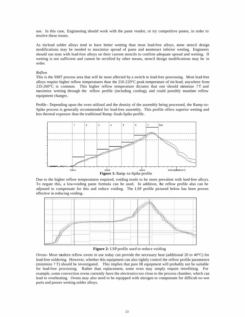
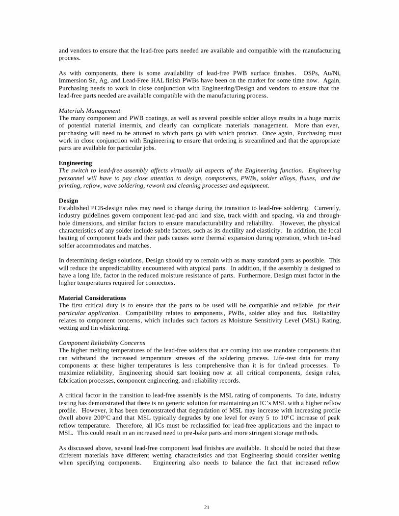
Figure 1: Ramp -to-Spike profile
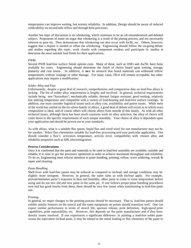
Figure 2: LSP profile used to reduce voiding
use. In this case, Engineering should work with the paste vendor, or try competitive pastes, in order to resolve these issues. As tin/lead solder alloys tend to have better wetting than most lead-free alloys, some stencil design modifications may be needed to maximize spread of paste and counteract inferior wetting. Engineers should run tests with lead-free alloys on their current stencils to confirm adequate spread and wetting. If wetting is not sufficient and cannot be rectified by other means, stencil design modifications may be in order. Reflow This is the SMT process area that will be most affected by a switch to lead-free processing. Most lead-free alloys require higher reflow temperatures than the 210-220°C peak temperature of tin/lead; anywhere from 235-260°C is common. This higher reflow temperature dictates that one should minimize ? T and maximize wetting through the reflow profile (including cooling), and could possibly mandate reflow equipment changes. Profile - Depending upon the oven utilized and the density of the assembly being processed, the Ramp -to-Spike process is generally recommended for lead-free assembly. This profile offers superior wetting and less thermal exposure than the traditional Ramp -Soak-Spike profile.
Due to the higher reflow temperatures required, voiding tends to be more prevalent with lead-free alloys. To negate this, a low-voiding paste formula can be used. In addition, the reflow profile also can be adjusted to compensate for this and reduce voiding. The LSP profile pictured below has been proven effective in reducing voiding.
Ovens- Most modern reflow ovens in use today can provide the necessary heat (additional 20 to 40°C) for lead-free soldering. However, whether this equipment can also tightly control the reflow profile parameters (minimize ? T) should be investigated. This implies that pure IR equipment will probably not be suitable for lead-free processing. Rather than replacement, some oven may simply require retrofitting. For example, some convection ovens currently have the electronics too close to the process chamber, which can lead to overheating. Ovens may also need to be equipped with nitrogen to compensate for difficult-to-wet parts and poorer wetting solder alloys.
23
Wave Soldering Depending upon the alloy selected, wave soldering will require a pot temperature of 260-275°C. This increase of temperature and the change in solder alloy will require some additional process changes. Flux- May require a change in liquid fluxes to compensate for the poor wetting of some alloys and high thermal stresses of the wave process. If changing fluxes, particular attention should be paid to both to operating window it offers and the material’s reliability characteristics. Equipment- Most modern wave solder machines can provide the necessary heat (preheat and wave) for lead-free soldering. However, as shown in figures 3 and 41, the high-tin lead-free alloys rapidly dissolve the materials often used in wave solder equipment. Stainless steel pots, nozzles, impellers and other parts will need to be replaced with cast iron and other materials available from wave soldering equipment manufacturers or be covered with an appropriate paint that should protect the parts for 2-3 years. In addition, a nitrogen blanket may be required, depending upon the alloy and flux selected.
Rework and Repair Materials - Operators must be re-trained for lead-free rework, as the lead-free solders do not flow as well as tin/lead. This could also require stronger cored wire fluxes to be used. As with any change of flux chemistry, if changing wire solders, particular attention should be paid to both to operating window it offers and the material’s reliability characteristics. Some wires often assumed to be safe to leave uncleaned are actually classified as rosin fully-activated and could cause field failures. All rework should use the same lead-free solder alloy as originally used on the solder joint; different lead-free solder formulations should not be mixed on the same joint. If more than one alloy is in use in the production process (i.e., Sn/Ag/Cu for SMT and Sn/Cu for wave soldering), operators should be trained to use the correct wire for each part. For this reason alone, it is advisable to use a single solder alloy for all assembly operations. Equipment- It is necessary to ensure that the desoldering and soldering stations are suitable for lead-free processing, i.e. can reach the necessary temperatures for lead-free soldering. It should be noted that lead-free soldering can wear out tips at a much higher rate than t in/lead. Cleaning In general, studies have demonstrated that post-process flux residues from lead-free applications are still cleanable. Water soluble chemistries may be cleaned in water, no-clean and RMA chemistries with a saponifier or cleaning solvent. However, it has been found that an increase in pressure, cleaning times and/or cleaner concentrations often is necessary. The efficiency of the cleaning equipment, strength of the cleaner, melting point of the alloy being used and thermal stability and propensity of the flux to “char” all affect the cleanability of an assembly.
1 Pictures courtesy of TWI/UK
Figure 3: Dissolved solder pot Figure 4: Dissolved impeller
24
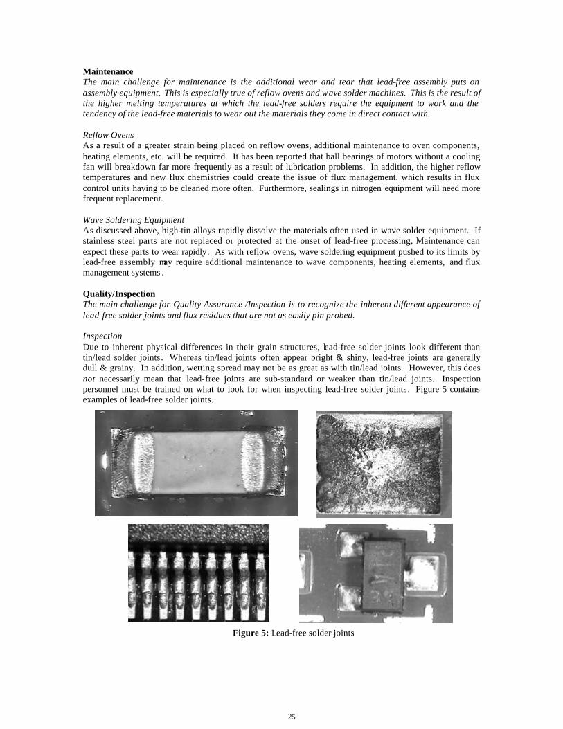
Maintenance The main challenge for maintenance is the additional wear and tear that lead-free assembly puts on assembly equipment. This is especially true of reflow ovens and wave solder machines. This is the result of the higher melting temperatures at which the lead-free solders require the equipment to work and the tendency of the lead-free materials to wear out the materials they come in direct contact with. Reflow Ovens As a result of a greater strain being placed on reflow ovens, additional maintenance to oven components, heating elements, etc. will be required. It has been reported that ball bearings of motors without a cooling fan will breakdown far more frequently as a result of lubrication problems. In addition, the higher reflow temperatures and new flux chemistries could create the issue of flux management, which results in flux control units having to be cleaned more often. Furthermore, sealings in nitrogen equipment will need more frequent replacement. Wave Soldering Equipment As discussed above, high-tin alloys rapidly dissolve the materials often used in wave solder equipment. If stainless steel parts are not replaced or protected at the onset of lead-free processing, Maintenance can expect these parts to wear rapidly. As with reflow ovens, wave soldering equipment pushed to its limits by lead-free assembly may require additional maintenance to wave components, heating elements, and flux management systems . Quality/Inspection The main challenge for Quality Assurance /Inspection is to recognize the inherent different appearance of lead-free solder joints and flux residues that are not as easily pin probed. Inspection Due to inherent physical differences in their grain structures, lead-free solder joints look different than tin/lead solder joints. Whereas tin/lead joints often appear bright & shiny, lead-free joints are generally dull & grainy. In addition, wetting spread may not be as great as with tin/lead joints. However, this does not necessarily mean that lead-free joints are sub-standard or weaker than tin/lead joints. Inspection personnel must be trained on what to look for when inspecting lead-free solder joints. Figure 5 contains examples of lead-free solder joints.
Figure 5: Lead-free solder joints
25
Pin Probe Testing Current test fixture settings could possibly damage lead-free solder joints. In addition, the higher reflow temperatures may result in charring and make probing through “pin probeable” flux residues more difficult. This could warrant changing flux chemistries or even residue removal in some cases. Conclusion A great deal of empirical information has been presented in order to help organizations implement lead-free soldering per their own time-line. Lead-free electronics assembly is achievable, but it requires a strong understanding of the changes required of each person involved in the manufacturing process. This pertains to considerations regarding design, components, PWBs, solder alloys, fluxes, printing, reflow, wave soldering, rework, cleaning, equipment wear & tear and inspection.
26
Materials and Process Considerations for Lead-Free Electronics Assembly
Karl Seelig and David Suraski November 2001
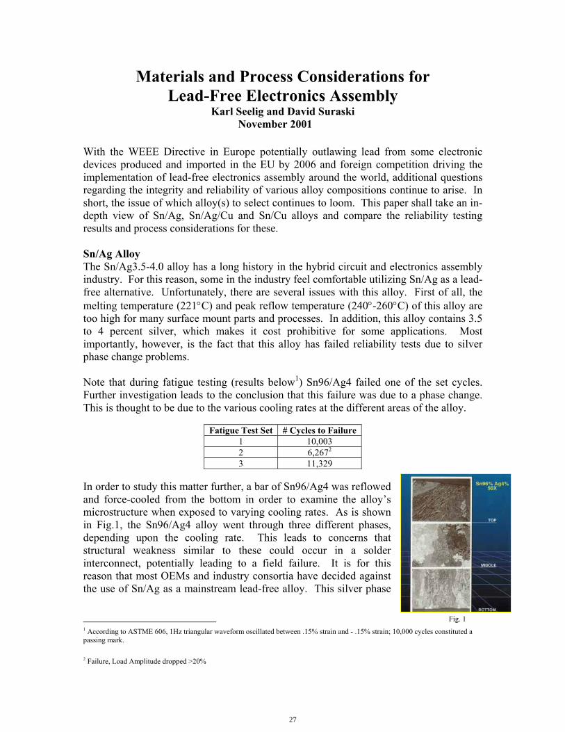
With the WEEE Directive in Europe potentially outlawing lead from some electronic devices produced and imported in the EU by 2006 and foreign competition driving the implementation of lead-free electronics assembly around the world, additional questions regarding the integrity and reliability of various alloy compositions continue to arise. In short, the issue of which alloy(s) to select continues to loom. This paper shall take an in-depth view of Sn/Ag, Sn/Ag/Cu and Sn/Cu alloys and compare the reliability testing results and process considerations for these. Sn/Ag Alloy The Sn/Ag3.5-4.0 alloy has a long history in the hybrid circuit and electronics assembly industry. For this reason, some in the industry feel comfortable utilizing Sn/Ag as a lead-free alternative. Unfortunately, there are several issues with this alloy. First of all, the melting temperature (221°C) and peak reflow temperature (240°-260°C) of this alloy are too high for many surface mount parts and processes. In addition, this alloy contains 3.5 to 4 percent silver, which makes it cost prohibitive for some applications. Most importantly, however, is the fact that this alloy has failed reliability tests due to silver phase change problems. Note that during fatigue testing (results below1) Sn96/Ag4 failed one of the set cycles. Further investigation leads to the conclusion that this failure was due to a phase change. This is thought to be due to the various cooling rates at the different areas of the alloy.
Fatigue Test Set # Cycles to Failure
1 10,003 2 6,2672 3 11,329
In order to study this matter further, a bar of Sn96/Ag4 was reflowed and force-cooled from the bottom in order to examine the alloy�s microstructure when exposed to varying cooling rates. As is shown in Fig.1, the Sn96/Ag4 alloy went through three different phases, depending upon the cooling rate. This leads to concerns that structural weakness similar to these could occur in a solder interconnect, potentially leading to a field failure. It is for this reason that most OEMs and industry consortia have decided against the use of Sn/Ag as a mainstream lead-free alloy. This silver phase
1 According to ASTME 606, 1Hz triangular waveform oscillated between .15% strain and - .15% strain; 10,000 cycles constituted a passing mark. 2 Failure, Load Amplitude dropped >20%
Fig. 1
27
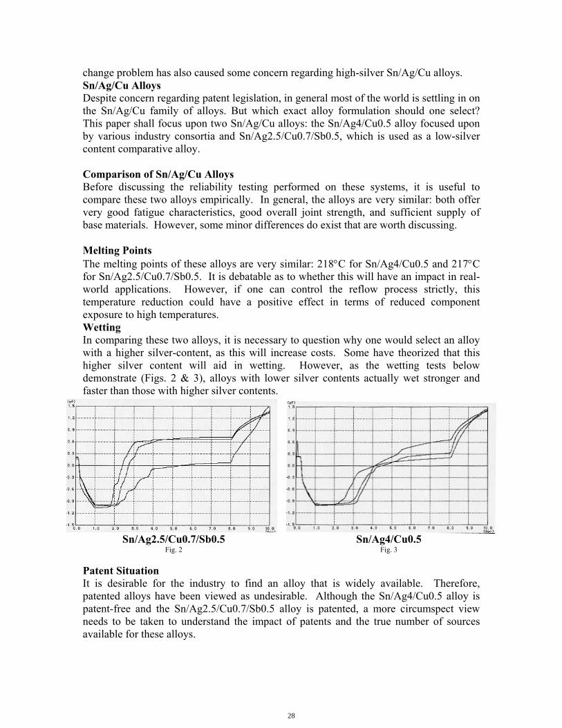
change problem has also caused some concern regarding high-silver Sn/Ag/Cu alloys. Sn/Ag/Cu Alloys Despite concern regarding patent legislation, in general most of the world is settling in on the Sn/Ag/Cu family of alloys. But which exact alloy formulation should one select? This paper shall focus upon two Sn/Ag/Cu alloys: the Sn/Ag4/Cu0.5 alloy focused upon by various industry consortia and Sn/Ag2.5/Cu0.7/Sb0.5, which is used as a low-silver content comparative alloy. Comparison of Sn/Ag/Cu Alloys Before discussing the reliability testing performed on these systems, it is useful to compare these two alloys empirically. In general, the alloys are very similar: both offer very good fatigue characteristics, good overall joint strength, and sufficient supply of base materials. However, some minor differences do exist that are worth discussing. Melting Points The melting points of these alloys are very similar: 218°C for Sn/Ag4/Cu0.5 and 217°C for Sn/Ag2.5/Cu0.7/Sb0.5. It is debatable as to whether this will have an impact in real-world applications. However, if one can control the reflow process strictly, this temperature reduction could have a positive effect in terms of reduced component exposure to high temperatures. Wetting In comparing these two alloys, it is necessary to question why one would select an alloy with a higher silver-content, as this will increase costs. Some have theorized that this higher silver content will aid in wetting. However, as the wetting tests below demonstrate (Figs. 2 & 3), alloys with lower silver contents actually wet stronger and faster than those with higher silver contents.
Patent Situation It is desirable for the industry to find an alloy that is widely available. Therefore, patented alloys have been viewed as undesirable. Although the Sn/Ag4/Cu0.5 alloy is patent-free and the Sn/Ag2.5/Cu0.7/Sb0.5 alloy is patented, a more circumspect view needs to be taken to understand the impact of patents and the true number of sources available for these alloys.
Sn/Ag2.5/Cu0.7/Sb0.5 Fig. 2
Sn/Ag4/Cu0.5 Fig. 3
28
As stated above, the Sn/Ag2.5/Cu0.7/Sb0.5 alloy is patented. However, it has been licensed to solder manufacturers with an unlimited number of licensees and no sign-on costs. Currently, the alloy is globally available through several North American, Japanese, and European-based solder manufacturers. Although the Sn/Ag4/Cu0.5 alloy is not patented, the users of this alloy should be aware that solder joints produced while using this alloy may be patented and the number of electronic-grade solder manufacturers able to sell this product under license in the U.S. is extremely limited. Alloys such as Sn/Ag4/Cu0.5 have been recommended to the industry despite the fact that solder joints produced from these may infringe existing patents; it has been assumed that since prior art exists on these systems that they are exempt from the patent. This is wrong, as most of the patents written have both alloy composition and application (solder joint) coverage. In other words, if prior art can be proven, it may be possible to beat the alloy composition section of the patent; however, if the patent is properly written it will also be necessary to challenge the application side that claims a unique use for soldering electronics assemblies. This is the section of the Ames Lab/Iowa State patent (# US05527628) that is probably enforceable and could potentially result in patent infringement. Basically, this means that even if a manufacturer is using an alloy outside of a patent range (such as Sn/Ag4/Cu0.5), if during manufacturing the alloy �picks up� base metals (normally copper) and forms an intermetallic that contains the elements covered under a patent, the manufacturer has violated that patent and may be subject to legal action. Cost of Metals The Iowa State patent claims a silver content of 3.5 to 7.7 percent. This high silver content results in a costly alloy in bulk solder form; to fill a wave soldering pot every 1% silver in solder is approximately an additional $.66/lb. (see table below). To combat this expense, some have suggested lead-free alloys that do not contain silver for wave soldering applications and a silver-containing alloy for surface mount applications. As discussed below, this is an approach likely to lead to failure due to the drawbacks of Sn/Cu and a dual alloy process.
Raw Cost of Metals Alloy Price3 Per Pound
Sn/Ag2.5/Cu0.7/Sb0.5 $4.01 Sn/Ag4/Cu0.5 $4.99
Sn/Ag4.7/Cu1.7 $5.40 Sn/Cu Process Drawbacks While it is logical to try to contain costs, there are several issues with Sn/Cu that must be considered. First, the melting temperature of this alloy is 227°C, which prohibits its use for many temperature-sensitive applications. In addition, as widely proven, this is a poorer wetting alloy as compared to other lead-free solders, which may mandate the use of nitrogen and aggressive fluxes for many applications and could result in wetting-related defects. Furthermore, Sn/Cu typically has lower capillary action to draw it into
3 U.S. Dollars, based upon cost of metals March 9, 2001
29
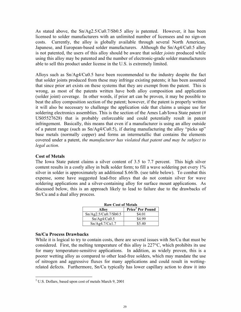
barrels during PTH technology and lacks the fatigue resistance needed for surface mount assembly. Finally, the poor fatigue characteristics of this alloy may result in field failures, which clearly negate any initial cost savings provided by this less-expensive alloy4. Dual Alloy Assembly It should also be noted that, in addition to the problems associated with Sn/Cu, the use of two solder alloys (i.e., Sn/Ag/Cu for SMT and Sn/Cu for wave soldering) could result in problems as well. It is undesirable to intermix Sn/Ag/Cu and Sn/Cu because this could result in non-uniformly alloyed solder joints. If this occurs the joint may be susceptible to fatigue failure due to its inability to stress and strain relieve. Because of these potential intermix problems, when repairs or touch-ups are required two inventories of alloys are needed and specific instructions need to be given and policed so as to not mix these alloys. Unfortunately, experience demonstrates that no mater how well this situation is policed, operators will tend to use the solder that is easiest to use, i.e., flows the best and has the lower melting temperature. Thus, it is likely that many joints will be touched up with the Sn/Ag/Cu alloy, even if these were originally assembled with Sn/Cu. This is analogous to no-clean and RA core wires; if these are both on the production floor the RA often gets used when it should not for the simple reason that it is easier to use. The bottom-line is that a dual alloy assembly process results in potential reliability problems and can be very difficult to police effectively. Solder Joint Reliability Testing In order to analyze the reliability of Sn/Cu and Sn/Ag/Cu alloys, these were subjected to various thermal and mechanical fatigue tests. The descriptions and results of these tests are below. Thermal Cycling Test Results Test boards were built using Sn/Cu0.7, Sn/Ag4/Cu0.5, and Sn/Ag2.5/Cu0.7/Sb0.5 in conjunction with 1206 thin film resistors. The boards were then thermal shocked from -40° to +125°C for 300, 400 and 500 15 minute cycles. Solder joints were then cross-sectioned and inspected for cracks. Post-test inspection shows that the Sn/Cu alloy exhibited some cracked solder joints as a result of poor wetting (Fig. 4). In addition, well-formed solder joints made from the Sn/Cu alloy also showed cracks on the third set of boards cycled to 500 repetitions (Fig. 5).
4Major OEMs have reported Sn/Cu joint failures due to both poor wetting and the alloy itself.
30
Fig. 6 Fig. 7
Fig. 8 Fig.10Fig. 9
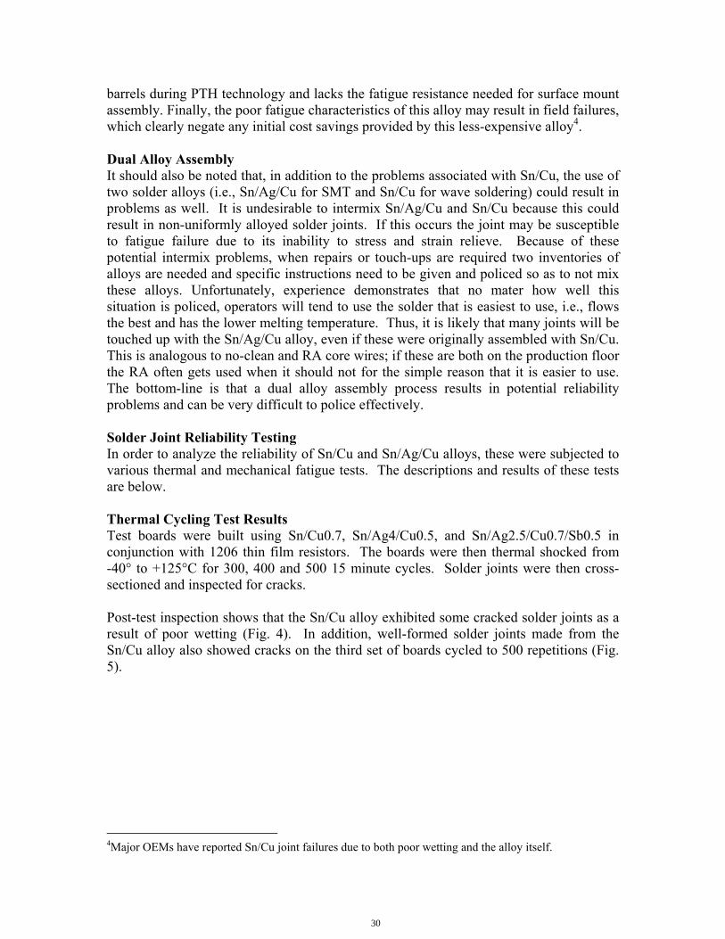
It is interesting to note that the Sn/Ag4/Cu0.5 (Fig. 6) and Sn/Ag2.5/Cu0.7/Sb0.5 (Fig. 7) alloys did not show any cracks during testing up to 500 repetitions. As this demonstrates, the Sn/Ag/Cu alloys have significantly superior thermal fatigue resistance as compared to Sn/Cu. However, as is apparent in Fig. 7, it should be noted that the Sn/Ag4/Cu0.5 alloy did exhibit some change in grain structure throughout the joint after thermal cycling.
Mechanical Strength- Flex Testing Test boards were built using Sn/Cu0.7, Sn/Ag4/Cu0.5, and Sn/Ag2.5/Cu0.7/Sb0.5 in conjunction with 1206 thin film resistors and were subjected to flex testing. As is shown in the images below, solder joints produced from Sn/Cu0.7 (Fig. 8) cracked during flex testing, which is indicative of a joint that cannot withstand a wide range of mechanical stresses. Contrarily, solder joints produced from Sn/Ag4/Cu0.5 (Fig. 9) and Sn/Ag2.5/Cu0.7/Sb0.5 (Fig. 10) passed all flex test requirements.
Fig. 4 Fig. 5
31

Drop-In Solution? Bance Hom5 is an independent consultant with Consultech International specializing in the semiconductor industry. To assuage fears within the electronics industry, Ms. Hom has developed a drop-in solution for complete lead-free assembly. In implementing a system using matte tin lead finishes (QFP 208 ICs), organic surface protectant PWBs, and a solder paste alloy of Sn/Ag2.5/Cu0.7/Sb0.5, Ms. Hom was able to produce completely lead-free assemblies without a dramatic increase in complexity or expense. Key to this success was that Ms. Hom was able to reflow these assemblies with a peak temperature of 234°C. It should be noted that these assemblies were processed in an inert environment. Of course, not all assemblies will be able to be processed as the above due to component availability issues and the fact that a 234°C peak board temperature may not be achievable on all assemblies due to varying ∆T�s resulting from component mass, fixturing devices, etc. However, it is important to note that in certain cases lead-free soldering may be painlessly achieved now with the implementation of certain materials. Conclusion A tremendous amount of interest exists in lead-free soldering. Much of this is derived from a fear of legislation and marketing activities. This has spurred a great deal of committee and consortia activity, some of which has been valuable to the industry. Several problems related to processing and reliability are associated with Sn/Cu alloys. In addition, difficulties arise when using two alloys to assemble a circuit board. As pointed out earlier, silver is the cost element in the Sn/Ag/Cu alloys. Since there are no advantages in terms of processing, reliability, or availability for the high-silver alloys as compared to the low-silver alloys, it is only logical to utilize the less expensive of these for use in all soldering applications. In fact, the low-silver alloys eliminate the potential for silver phase change problems with high-silver alloys and offer improved wetting and a slightly lower melting temperature. These alloys are available from several solder manufacturers throughout the world and have been recommended for widespread use in Japan by the JEIDA industry organization. Most importantly, the low-silver Sn/Ag/Cu alloys provides users with the advantages of the Sn/Ag/Cu family of alloys, are less cost-prohibitive and therefore may be utilized in all solder operations, and thus eliminate the problems associated with Sn/Cu alloys and a dual-alloy process. For additional information, please contact the authors at 800-CALL-AIM, 401-463-5605 or [email protected]
5 Bance Hom may be reached at (510) 743-1956 or [email protected]
32
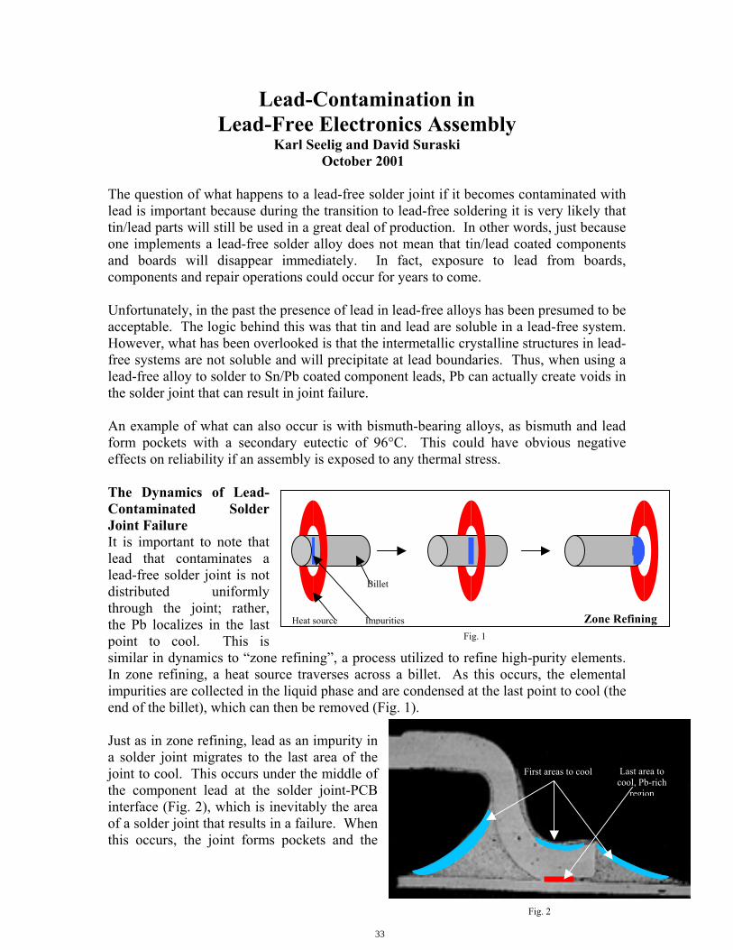
Heat source Impurities
Billet
Zone RefiningFig. 1
Lead-Contamination in Lead-Free Electronics Assembly
Karl Seelig and David Suraski October 2001
The question of what happens to a lead-free solder joint if it becomes contaminated with lead is important because during the transition to lead-free soldering it is very likely that tin/lead parts will still be used in a great deal of production. In other words, just because one implements a lead-free solder alloy does not mean that tin/lead coated components and boards will disappear immediately. In fact, exposure to lead from boards, components and repair operations could occur for years to come. Unfortunately, in the past the presence of lead in lead-free alloys has been presumed to be acceptable. The logic behind this was that tin and lead are soluble in a lead-free system. However, what has been overlooked is that the intermetallic crystalline structures in lead-free systems are not soluble and will precipitate at lead boundaries. Thus, when using a lead-free alloy to solder to Sn/Pb coated component leads, Pb can actually create voids in the solder joint that can result in joint failure. An example of what can also occur is with bismuth-bearing alloys, as bismuth and lead form pockets with a secondary eutectic of 96°C. This could have obvious negative effects on reliability if an assembly is exposed to any thermal stress. The Dynamics of Lead-Contaminated Solder Joint Failure It is important to note that lead that contaminates a lead-free solder joint is not distributed uniformly through the joint; rather, the Pb localizes in the last point to cool. This is similar in dynamics to �zone refining�, a process utilized to refine high-purity elements. In zone refining, a heat source traverses across a billet. As this occurs, the elemental impurities are collected in the liquid phase and are condensed at the last point to cool (the end of the billet), which can then be removed (Fig. 1). Just as in zone refining, lead as an impurity in a solder joint migrates to the last area of the joint to cool. This occurs under the middle of the component lead at the solder joint-PCB interface (Fig. 2), which is inevitably the area of a solder joint that results in a failure. When this occurs, the joint forms pockets and the
First areas to cool Last area to cool, Pb-rich
region
Fig. 2
33
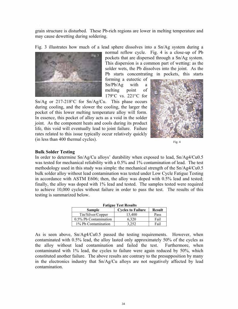
grain structure is disturbed. These Pb-rich regions are lower in melting temperature and may cause dewetting during soldering. Fig. 3 illustrates how much of a lead sphere dissolves into a Sn/Ag system during a
normal reflow cycle. Fig. 4 is a close-up of Pb pockets that are dispersed through a Sn/Ag system. This dispersion is a common part of wetting: as the solder wets, the Pb dissolves into the joint. As the Pb starts concentrating in pockets, this starts forming a eutectic of Sn/Pb/Ag with a melting point of 179°C vs. 221°C for
Sn/Ag or 217-218°C for Sn/Ag/Cu. This phase occurs during cooling, and the slower the cooling, the larger the pocket of this lower melting temperature alloy will form. In essence, this pocket of alloy acts as a void in the solder joint. As the component heats and cools during its product life, this void will eventually lead to joint failure. Failure rates related to this issue typically occur relatively quickly (in less than 400 thermal cycles). Bulk Solder Testing In order to determine Sn/Ag/Cu alloys� durability when exposed to lead, Sn/Ag4/Cu0.5 was tested for mechanical reliability with a 0.5% and 1% contamination of lead. The test methodology used in this study was simple: the mechanical strength of the Sn/Ag4/Cu0.5 bulk solder alloy without lead contamination was tested under Low Cycle Fatigue Testing in accordance with ASTM E606; then, the alloy was doped with 0.5% lead and tested; finally, the alloy was doped with 1% lead and tested. The samples tested were required to achieve 10,000 cycles without failure in order to pass the test. The results of this testing is summarized below.
Fatigue Test Results Sample Cycles to Failure Result
Tin/Silver/Copper 13,400 Pass 0.5% Pb Contamination 6,320 Fail 1% Pb Contamination 3,252 Fail
As is seen above, Sn/Ag4/Cu0.5 passed the testing requirements. However, when contaminated with 0.5% lead, the alloy lasted only approximately 50% of the cycles as the alloy without lead contamination and failed the test. Furthermore, when contaminated with 1% lead, the cycles to failure were again reduced by 50%, which constituted another failure. The above results are contrary to the presupposition by many in the electronics industry that Sn/Ag/Cu alloys are not negatively affected by lead contamination.
Fig. 4
Fig. 3
34
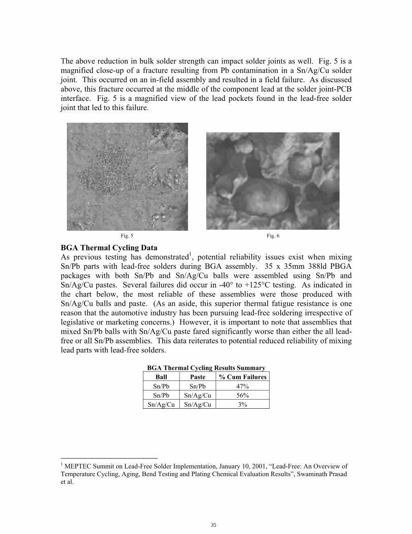
The above reduction in bulk solder strength can impact solder joints as well. Fig. 5 is a magnified close-up of a fracture resulting from Pb contamination in a Sn/Ag/Cu solder joint. This occurred on an in-field assembly and resulted in a field failure. As discussed above, this fracture occurred at the middle of the component lead at the solder joint-PCB interface. Fig. 5 is a magnified view of the lead pockets found in the lead-free solder joint that led to this failure.
BGA Thermal Cycling Data As previous testing has demonstrated1, potential reliability issues exist when mixing Sn/Pb parts with lead-free solders during BGA assembly. 35 x 35mm 388ld PBGA packages with both Sn/Pb and Sn/Ag/Cu balls were assembled using Sn/Pb and Sn/Ag/Cu pastes. Several failures did occur in -40° to +125°C testing. As indicated in the chart below, the most reliable of these assemblies were those produced with Sn/Ag/Cu balls and paste. (As an aside, this superior thermal fatigue resistance is one reason that the automotive industry has been pursuing lead-free soldering irrespective of legislative or marketing concerns.) However, it is important to note that assemblies that mixed Sn/Pb balls with Sn/Ag/Cu paste fared significantly worse than either the all lead-free or all Sn/Pb assemblies. This data reiterates to potential reduced reliability of mixing lead parts with lead-free solders.
BGA Thermal Cycling Results Summary Ball Paste % Cum Failures
Sn/Pb Sn/Pb 47% Sn/Pb Sn/Ag/Cu 56%
Sn/Ag/Cu Sn/Ag/Cu 3%
1 MEPTEC Summit on Lead-Free Solder Implementation, January 10, 2001, �Lead-Free: An Overview of Temperature Cycling, Aging, Bend Testing and Plating Chemical Evaluation Results�, Swaminath Prasad et al.
Fig. 5 Fig. 6
35
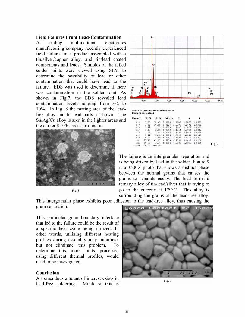
Field Failures From Lead-Contamination A leading multinational electronics manufacturing company recently experienced field failures in a product assembled with a tin/silver/copper alloy, and tin/lead coated components and leads. Samples of the failed solder joints were viewed using SEM to determine the possibility of lead or other contamination that could have lead to the failure. EDS was used to determine if there was contamination in the solder joint. As shown in Fig.7, the EDS revealed lead contamination levels ranging from 3% to 10%. In Fig. 8 the mating area of the lead-free alloy and tin-lead parts is shown. The Sn/Ag/Cu alloy is seen in the lighter areas and the darker Sn/Pb areas surround it.
The failure is an intergranular separation and is being driven by lead in the solder. Figure 9 is a 3500X photo that shows a distinct phase between the normal grains that causes the grains to separate easily. The lead forms a ternary alloy of tin/lead/silver that is trying to go to the eutectic at 179°C. This alloy is surrounding the grains of the lead-free alloy.
This intergranular phase exhibits poor adhesion to the lead-free alloy, thus causing the grain separation. This particular grain boundary interface that led to the failure could be the result of a specific heat cycle being utilized. In other words, utilizing different heating profiles during assembly may minimize, but not eliminate, this problem. To determine this, more joints, processed using different thermal profiles, would need to be investigated. Conclusion A tremendous amount of interest exists in lead-free soldering. Much of this is
Fig. 7
Fig. 9
Fig. 8
36
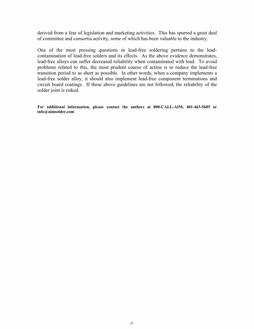
derived from a fear of legislation and marketing activities. This has spurred a great deal of committee and consortia activity, some of which has been valuable to the industry. One of the most pressing questions in lead-free soldering pertains to the lead-contamination of lead-free solders and its effects. As the above evidence demonstrates, lead-free alloys can suffer decreased reliability when contaminated with lead. To avoid problems related to this, the most prudent course of action is to reduce the lead-free transition period to as short as possible. In other words, when a company implements a lead-free solder alloy, it should also implement lead-free component terminations and circuit board coatings. If these above guidelines are not followed, the reliability of the solder joint is risked. For additional information, please contact the authors at 800-CALL-AIM, 401-463-5605 or [email protected]
37
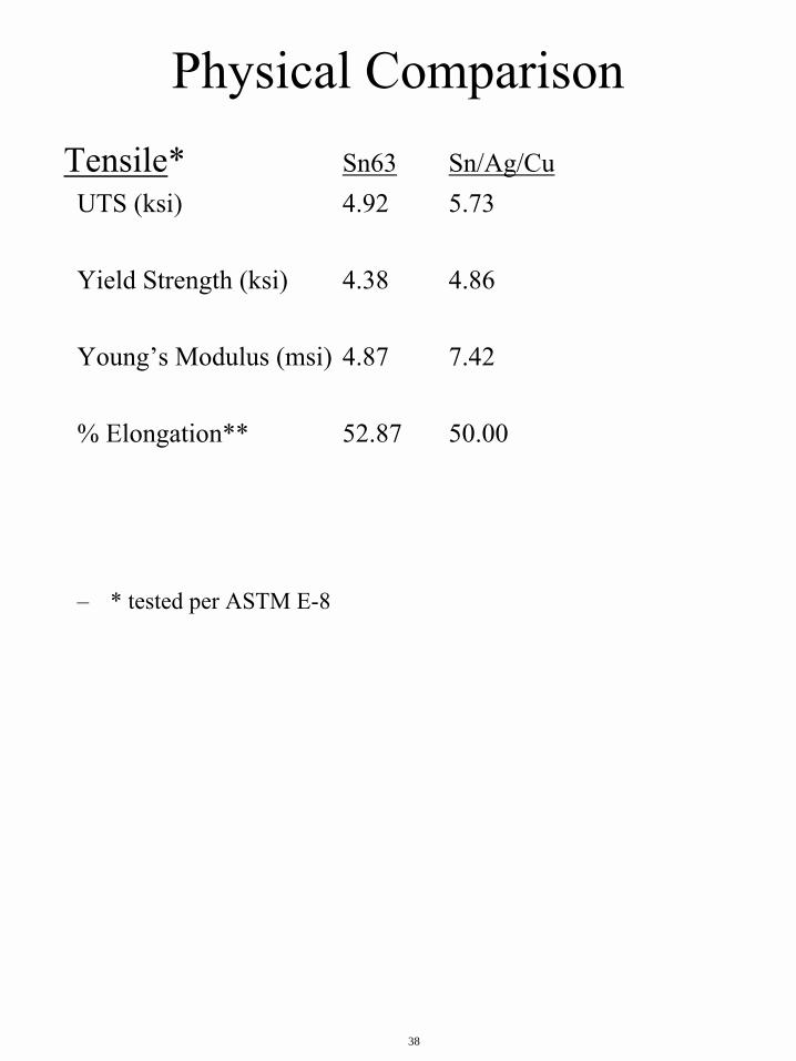
Physical ComparisonTensile* Sn63 Sn/Ag/Cu
UTS (ksi) 4.92 5.73
Yield Strength (ksi) 4.38 4.86
Young�s Modulus (msi) 4.87 7.42
% Elongation** 52.87 50.00
� * tested per ASTM E-8
38
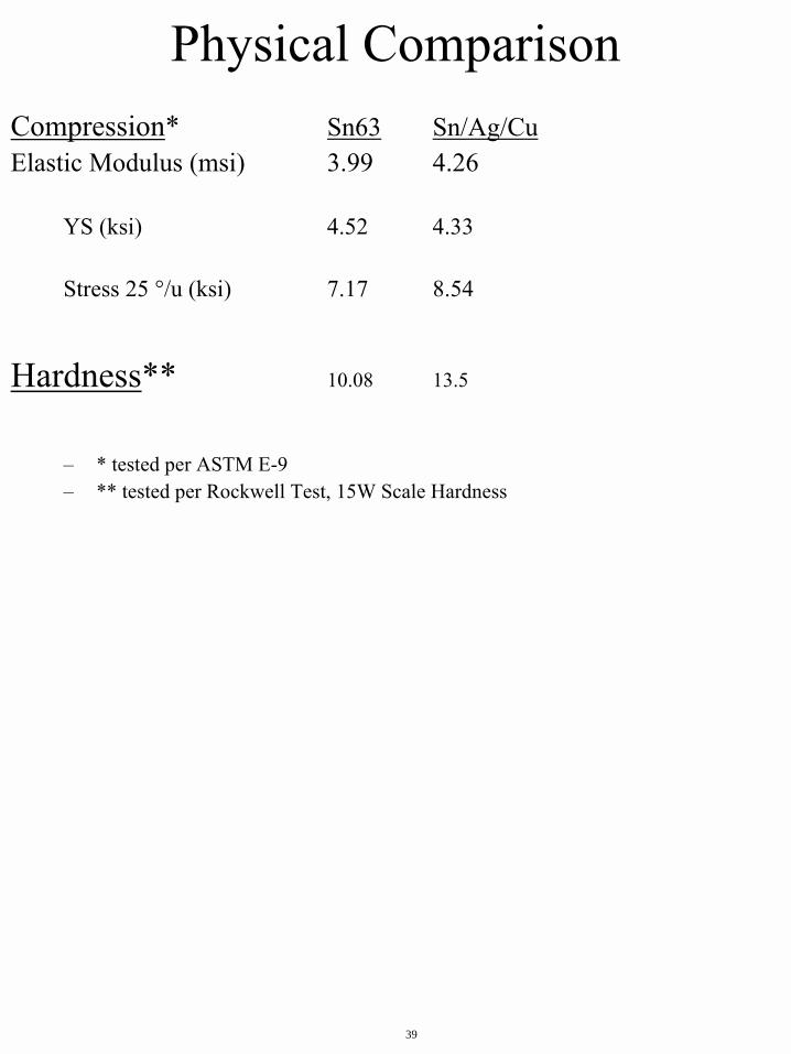
Physical ComparisonCompression* Sn63 Sn/Ag/CuElastic Modulus (msi) 3.99 4.26
YS (ksi) 4.52 4.33
Stress 25 °/u (ksi) 7.17 8.54
Hardness** 10.08 13.5
� * tested per ASTM E-9� ** tested per Rockwell Test, 15W Scale Hardness
39
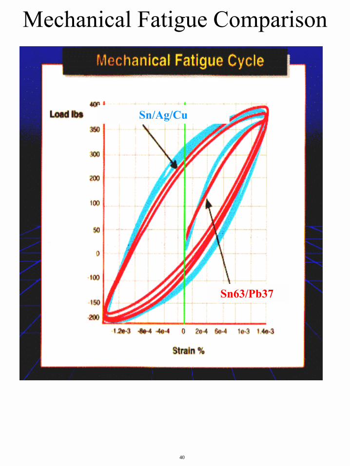
Sn/Ag/Cu
Sn63/Pb37
Mechanical Fatigue Comparison
40

Sn/Ag/Cu Sn63/Pb37
Strain Relieving Characteristics
41
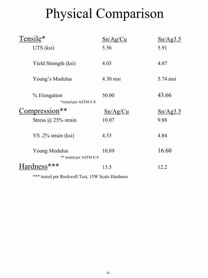
Physical Comparison
Tensile* Sn/Ag/Cu Sn/Ag3.5UTS (ksi) 5.56 5.91
Yield Strength (ksi) 4.03 4.07
Young�s Modulus 4.30 msi 5.74 msi
% Elongation 50.00 43.66*tested per ASTM E-8
Compression** Sn/Ag/Cu Sn/Ag3.5Stress @ 25% strain 10.07 9.88
YS .2% strain (ksi) 4.53 4.84
Young Modulus 10.89 16.60 ** tested per ASTM E-9
Hardness*** 13.5 12.2
*** tested per Rockwell Test, 15W Scale Hardness
42
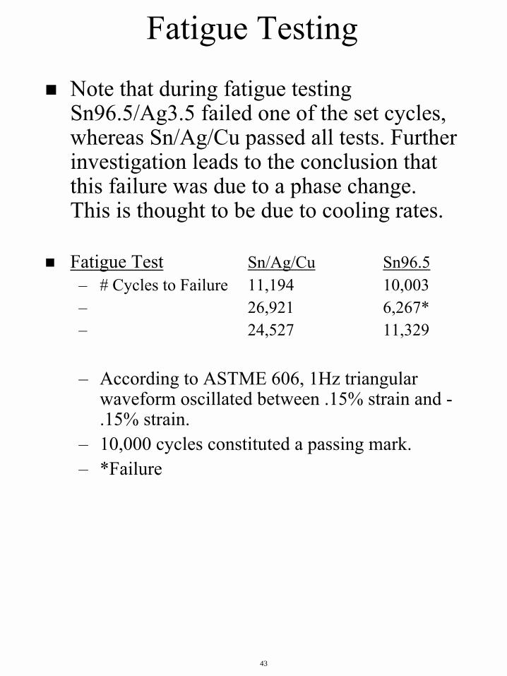
Fatigue Testing
! Note that during fatigue testing Sn96.5/Ag3.5 failed one of the set cycles, whereas Sn/Ag/Cu passed all tests. Further investigation leads to the conclusion that this failure was due to a phase change. This is thought to be due to cooling rates.
! Fatigue Test Sn/Ag/Cu Sn96.5� # Cycles to Failure 11,194 10,003� 26,921 6,267*� 24,527 11,329
� According to ASTME 606, 1Hz triangular waveform oscillated between .15% strain and -.15% strain.
� 10,000 cycles constituted a passing mark.� *Failure
43
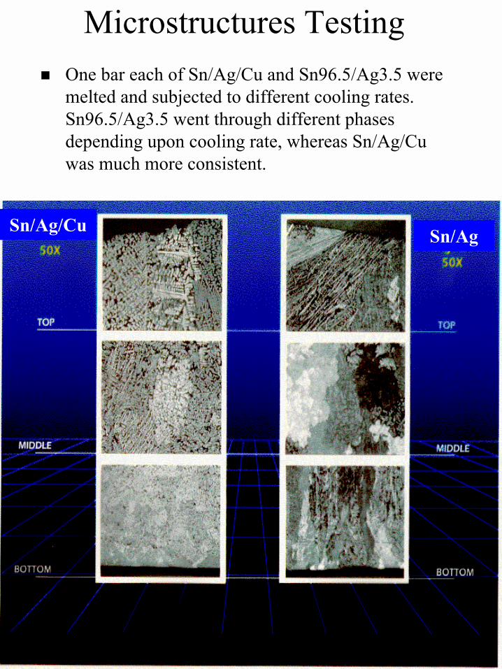
! One bar each of Sn/Ag/Cu and Sn96.5/Ag3.5 were melted and subjected to different cooling rates. Sn96.5/Ag3.5 went through different phases depending upon cooling rate, whereas Sn/Ag/Cu was much more consistent.
Microstructures Testing
Sn/Ag/Cu Sn/Ag
44
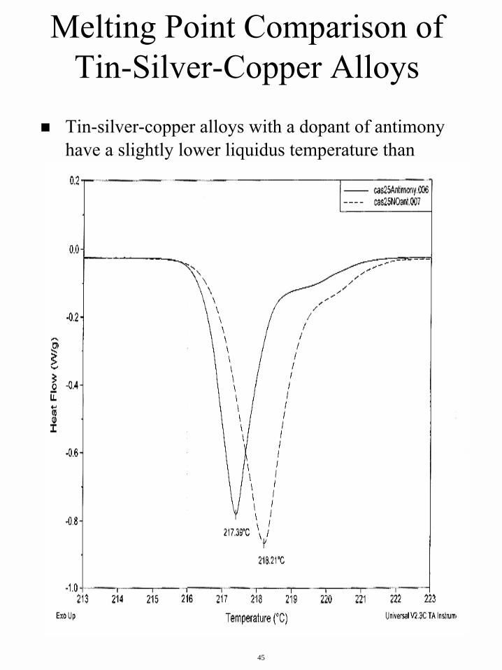
Melting Point Comparison of Tin-Silver-Copper Alloys
! Tin-silver-copper alloys with a dopant of antimonyhave a slightly lower liquidus temperature than those without
45
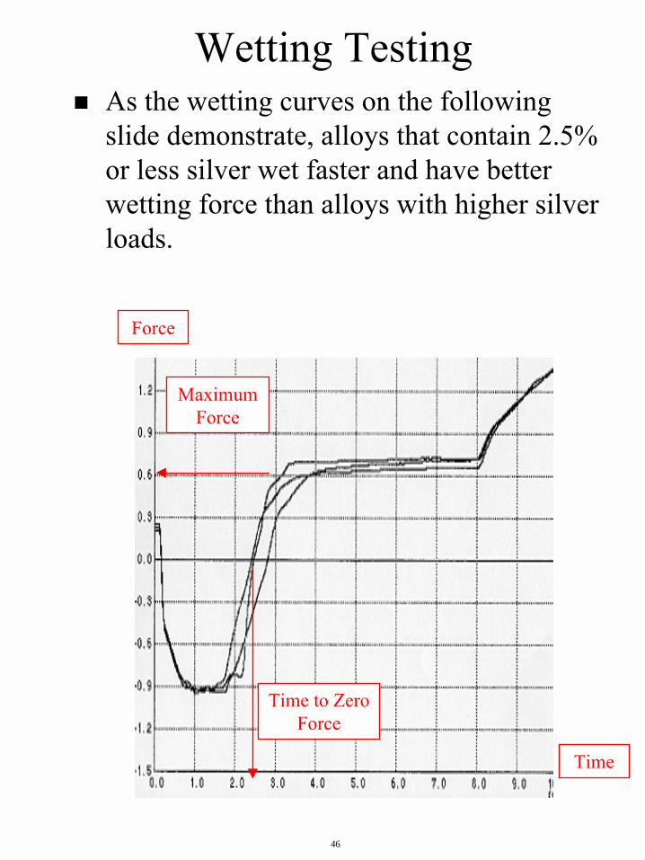
Wetting Testing! As the wetting curves on the following
slide demonstrate, alloys that contain 2.5% or less silver wet faster and have better wetting force than alloys with higher silver loads.
Time
Time to Zero Force
Maximum Force
Force
46
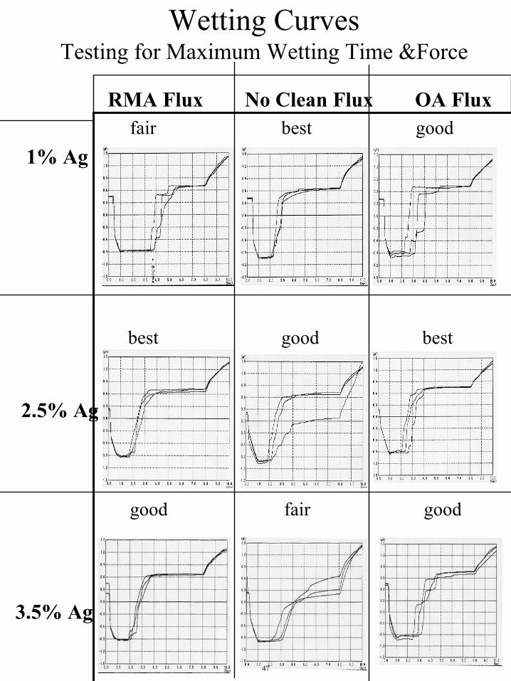
Wetting Curves Testing for Maximum Wetting Time &Force
RMA Flux No Clean Flux OA Fluxfair best good
1% Ag
best good best
2.5% Ag
good fair good
3.5% Ag
47
Thermal Cycling Testing
! Test boards were built using Sn/Cu0.7, Sn/Ag4/Cu0.5, and Sn/Ag2.5/Cu0.7/Sb0.5 in conjunction with 1206 thin film resistors. The boards were then thermal shocked from -40° to +125°C for 300, 400 and 500 15 minute cycles. Solder joints were then cross-sectioned and inspected for cracks.
48
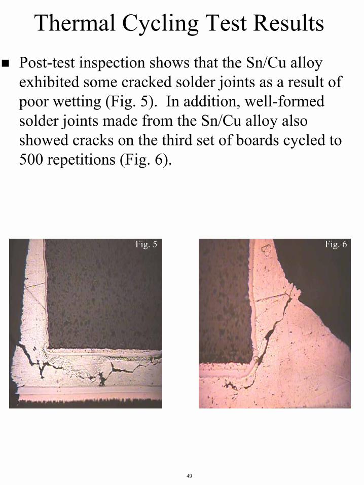
Thermal Cycling Test Results! Post-test inspection shows that the Sn/Cu alloy
exhibited some cracked solder joints as a result of poor wetting (Fig. 5). In addition, well-formed solder joints made from the Sn/Cu alloy also showed cracks on the third set of boards cycled to 500 repetitions (Fig. 6).
Fig. 5 Fig. 6
49
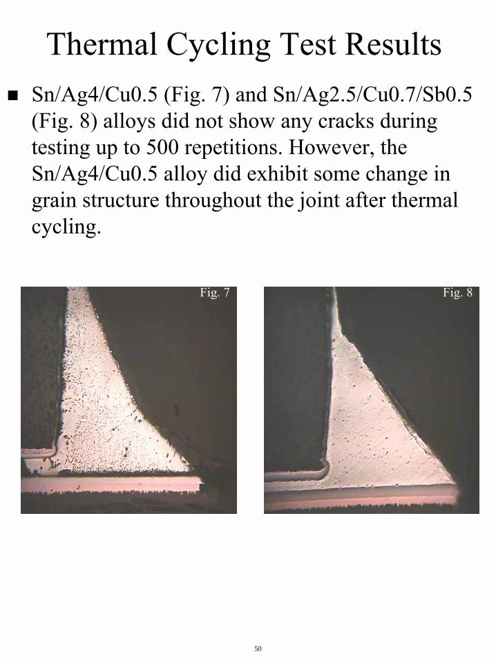
Thermal Cycling Test Results! Sn/Ag4/Cu0.5 (Fig. 7) and Sn/Ag2.5/Cu0.7/Sb0.5
(Fig. 8) alloys did not show any cracks during testing up to 500 repetitions. However, the Sn/Ag4/Cu0.5 alloy did exhibit some change in grain structure throughout the joint after thermal cycling.
Fig. 7 Fig. 8
50
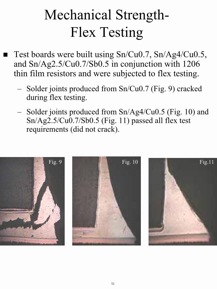
Mechanical Strength-Flex Testing
! Test boards were built using Sn/Cu0.7, Sn/Ag4/Cu0.5, and Sn/Ag2.5/Cu0.7/Sb0.5 in conjunction with 1206 thin film resistors and were subjected to flex testing.
� Solder joints produced from Sn/Cu0.7 (Fig. 9) cracked during flex testing.
� Solder joints produced from Sn/Ag4/Cu0.5 (Fig. 10) and Sn/Ag2.5/Cu0.7/Sb0.5 (Fig. 11) passed all flex test requirements (did not crack).
Fig. 9 Fig.11 Fig. 10
51

! The mechanical strength of the Sn/Ag4/Cu0.5 bulk solder alloy without lead contamination was tested under Low Cycle Fatigue Testing in accordance with ASTM E606*; then, the alloy was doped with 0.5% lead and tested; finally, the alloy was doped with 1% lead and tested. � *According to ASTM E606, 1Hz triangular waveform
oscillated between 0.15% strain and -0.15% strain.� 10,000 cycles constituted a passing mark.
Bulk Lead Contaminated Solder Testing
SampleSample Cycles to FailureCycles to Failure ResultResult
Tin/Silver/CopperTin/Silver/Copper 13,40013,400 PassPass
0.5% Pb Contamination
0.5% Pb Contamination
6,3206,320 FailFail
1% Pb Contamination
1% Pb Contamination
3,2523,252 FailFail
52
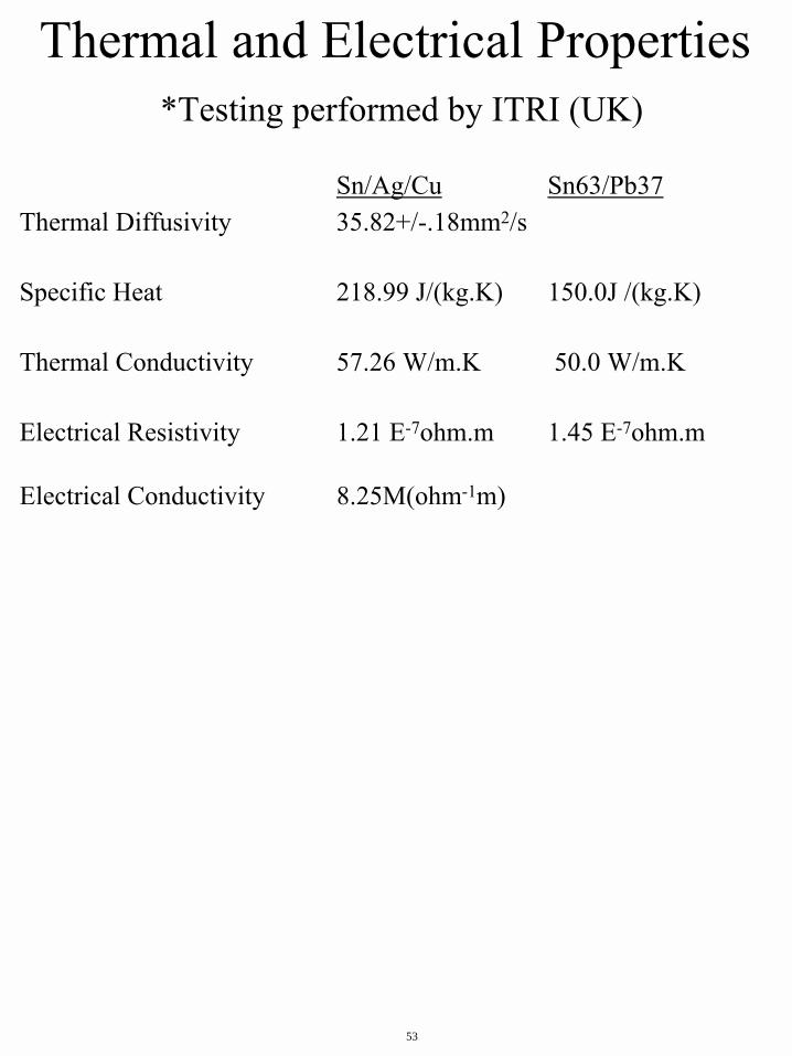
Thermal and Electrical Properties*Testing performed by ITRI (UK)
Sn/Ag/Cu Sn63/Pb37Thermal Diffusivity 35.82+/-.18mm2/s
Specific Heat 218.99 J/(kg.K) 150.0J /(kg.K)
Thermal Conductivity 57.26 W/m.K 50.0 W/m.K
Electrical Resistivity 1.21 E-7ohm.m 1.45 E-7ohm.m
Electrical Conductivity 8.25M(ohm-1m)
53
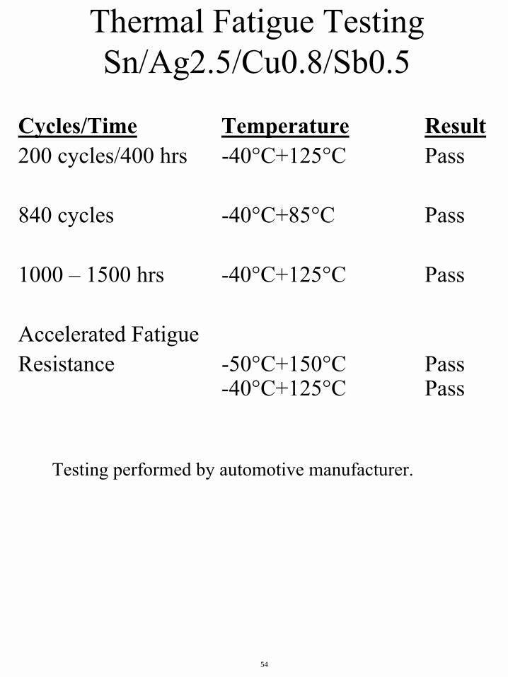
Thermal Fatigue Testing Sn/Ag2.5/Cu0.8/Sb0.5
Cycles/Time Temperature Result200 cycles/400 hrs -40°C+125°C Pass
840 cycles -40°C+85°C Pass
1000 � 1500 hrs -40°C+125°C Pass
Accelerated Fatigue Resistance -50°C+150°C Pass
-40°C+125°C Pass
Testing performed by automotive manufacturer.
54
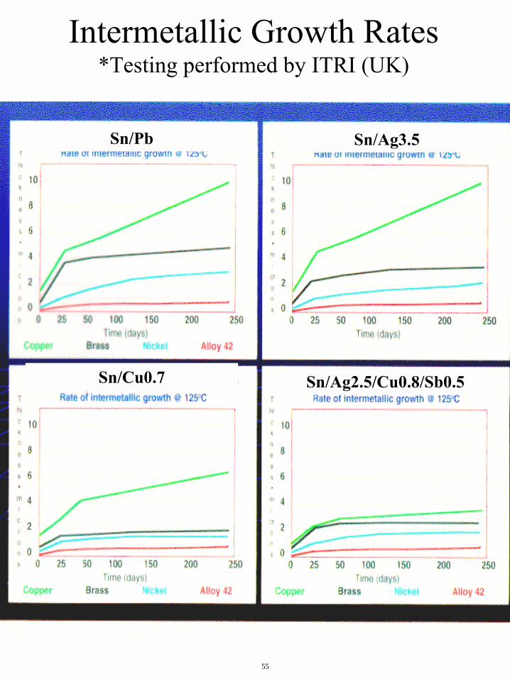
Intermetallic Growth Rates*Testing performed by ITRI (UK)
Sn/Ag2.5/Cu0.8/Sb0.5
Sn/Ag3.5Sn/Pb
Sn/Cu0.7
55
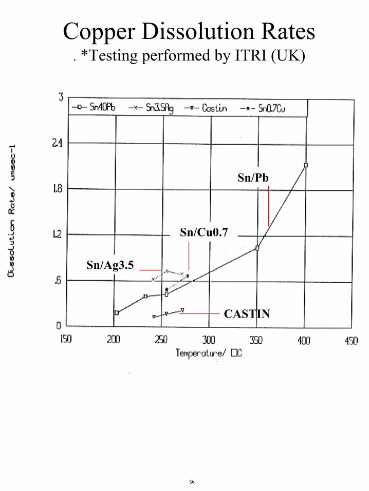
Copper Dissolution Rates. *Testing performed by ITRI (UK)
Sn/Pb
Sn/Ag3.5
Sn/Cu0.7
CASTIN
56
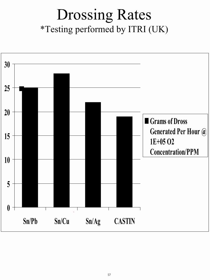
Drossing Rates*Testing performed by ITRI (UK)
0
5
10
15
20
25
30
Sn/Pb Sn/Cu Sn/Ag CASTIN
Grams of DrossGenerated Per Hour @1E+05 O2Concentration/PPM
!
57
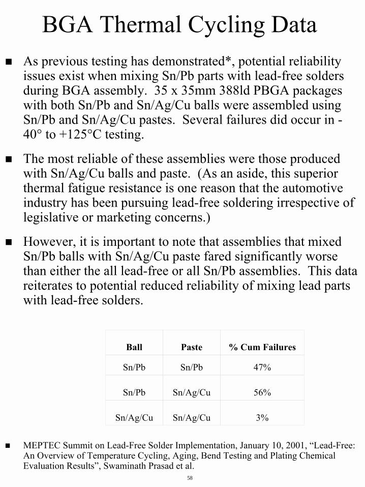
BGA Thermal Cycling Data! As previous testing has demonstrated*, potential reliability
issues exist when mixing Sn/Pb parts with lead-free solders during BGA assembly. 35 x 35mm 388ld PBGA packages with both Sn/Pb and Sn/Ag/Cu balls were assembled using Sn/Pb and Sn/Ag/Cu pastes. Several failures did occur in -40° to +125°C testing.
! The most reliable of these assemblies were those produced with Sn/Ag/Cu balls and paste. (As an aside, this superior thermal fatigue resistance is one reason that the automotive industry has been pursuing lead-free soldering irrespective of legislative or marketing concerns.)
! However, it is important to note that assemblies that mixed Sn/Pb balls with Sn/Ag/Cu paste fared significantly worse than either the all lead-free or all Sn/Pb assemblies. This data reiterates to potential reduced reliability of mixing lead partswith lead-free solders.
! MEPTEC Summit on Lead-Free Solder Implementation, January 10, 2001, �Lead-Free: An Overview of Temperature Cycling, Aging, Bend Testing and Plating Chemical Evaluation Results�, Swaminath Prasad et al.
BallBall PastePaste % Cum Failures% Cum Failures
Sn/PbSn/Pb Sn/PbSn/Pb 47%47%
Sn/PbSn/Pb Sn/Ag/CuSn/Ag/Cu 56%56%
Sn/Ag/CuSn/Ag/Cu Sn/Ag/CuSn/Ag/Cu 3%3%
58