Embed Size (px)
Citation preview
Lead halide perovskite solar cells
Citation for published version (APA):Bruijnaers, B. J. (2018). Lead halide perovskite solar cells Eindhoven: Technische Universiteit Eindhoven
Document status and date:Published: 28/06/2018
Document Version:Publisher’s PDF, also known as Version of Record (includes final page, issue and volume numbers)
Please check the document version of this publication:
• A submitted manuscript is the author's version of the article upon submission and before peer-review. Therecan be important differences between the submitted version and the official published version of record. Peopleinterested in the research are advised to contact the author for the final version of the publication, or visit theDOI to the publisher's website.• The final author version and the galley proof are versions of the publication after peer review.• The final published version features the final layout of the paper including the volume, issue and pagenumbers.Link to publication
General rightsCopyright and moral rights for the publications made accessible in the public portal are retained by the authors and/or other copyright ownersand it is a condition of accessing publications that users recognise and abide by the legal requirements associated with these rights.
• Users may download and print one copy of any publication from the public portal for the purpose of private study or research. • You may not further distribute the material or use it for any profit-making activity or commercial gain • You may freely distribute the URL identifying the publication in the public portal.
Take down policyIf you believe that this document breaches copyright please contact us:
providing details. We will immediately remove access to the work pending the investigation of your claim.
Download date: 07. Feb. 2019
Lead Halide Perovskite Solar Cells
PROEFSCHRIFT
ter verkrijging van de graad van doctor aan de Technische Universiteit Eindhoven,
op gezag van de rector magnificus prof.dr.ir. F.P.T. Baaijens, voor een commissie
aangewezen door het College voor Promoties, in het openbaar te verdedigen op
donderdag 28 juni 2018 om 13:30 uur
door
Bernardo Joseph Bruijnaers
Geboren te Weert

Dit proefschrift is goedgekeurd door de promotoren en de samenstelling van de
promotiecomissie is als volgt:
voorzitter: prof. dr. E. W. Meijer 1e promotor: prof. dr. ir. R. A. J. Janssen copromotor: dr. ir. M. M. Wienk leden: prof. dr. M. A. Loi (Rijksuniversiteit Groningen) prof. dr. ir. A. H. M. Smets (Technische Universiteit Delft) dr. M. Creatore prof. dr. E. P. A. M. Bakkers adviseur: dr. Y. Galagan (Solliance – TNO)
Het onderzoek of ontwerp dat in dit proefschrift wordt beschreven is uitgevoerd in
overeenstemming met de TU/e Gedragscode Wetenschapsbeoefening.
Lead Halide Perovskite Solar Cells
Bardo Bruijnaers

Printed by: Gildeprint, Enschede
A catalogue record is availible from the Eindhoven University of Technology
Library.
ISBN: 978-90-386-4507-0
The research described in this thesis has been financially supported by the
European Research Council under the European Seventh Framework Programme
FP(2007-2013)/ERC Grant Agreement No. 339031
Table of Contents
Chapter 1: Introduction 1
Chapter 2: Correct characterization of metal halide perovskite solar cells
31
Chapter 3: Perovskite layer crystallization tuning for maximizing solar cell efficiency
61
Chapter 4: The effect of oxygen on the efficiency of planar p-i-n metal halide perovskite solar cells with a PEDOT:PSS hole transport layer
89
Chapter 5: Vapor assisted solution processing of lead halide perovskite solar cells
117
Epilogue 161
Summary 165
Samenvatting 169
Curriculum Vitae 173
Dankwoord 179


Chapter 1
Introduction
Abstract
In this chapter, a short introduction about the necessity of using solar power is
followed by explanation of basic solar cell operation. Perovskite solar cells are discussed
in more detail by first giving an overview of the historic development of this relatively
new technology, after which the possibilities with the variation in composition of the
perovskite semiconductor are presented. Perovskite solar cell architectures and
processing methods are explained and advantages and challenges of the technology are
commented on. At the end of this chapter, the aim and outline of this thesis are clarified.
Chapter 1
2
1.1 Introduction
With the growing global population and economy, the energy demand is
increasing substantially, with a projected increase of energy consumption of ~28%
from 169 PWh in 2015 to 216 PWh in 2040.1 Especially countries with strong growing
economies like China and India contribute to this increase.1 Although renewable
energy is the world’s fastest growing energy source, the majority (77%) of energy is
still expected to be generated by burning fossil fuels in 2040.1
Even though the burning of fossil fuels is an easy way to generate energy, the
effects this has on our planet are serious. Looking at results from simulations and
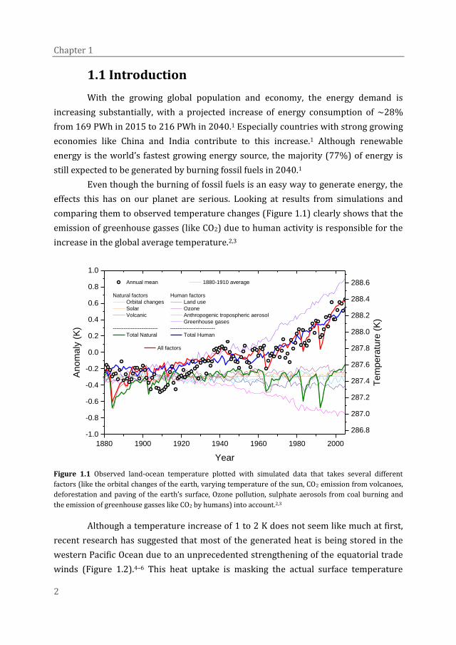
comparing them to observed temperature changes (Figure 1.1) clearly shows that the
emission of greenhouse gasses (like CO2) due to human activity is responsible for the
increase in the global average temperature.2,3
286.8
287.0
287.2
287.4
287.6
287.8
288.0
288.2
288.4
288.6
Tem
pe
ratu
re (
K)
1880 1900 1920 1940 1960 1980 2000
-1.0
-0.8
-0.6
-0.4
-0.2
0.0
0.2
0.4
0.6
0.8
1.0
Annual mean 1880-1910 average
Natural factors Human factors
Orbital changes Land use
Solar Ozone
Volcanic Anthropogenic tropospheric aerosol
Greenhouse gases
------------------------- -------------------------
Total Natural Total Human
All factors
Year
An
om
aly
(K
)
Figure 1.1 Observed land-ocean temperature plotted with simulated data that takes several different
factors (like the orbital changes of the earth, varying temperature of the sun, CO2 emission from volcanoes,
deforestation and paving of the earth’s surface, Ozone pollution, sulphate aerosols from coal burning and
the emission of greenhouse gasses like CO2 by humans) into account.2,3
Although a temperature increase of 1 to 2 K does not seem like much at first,
recent research has suggested that most of the generated heat is being stored in the
western Pacific Ocean due to an unprecedented strengthening of the equatorial trade
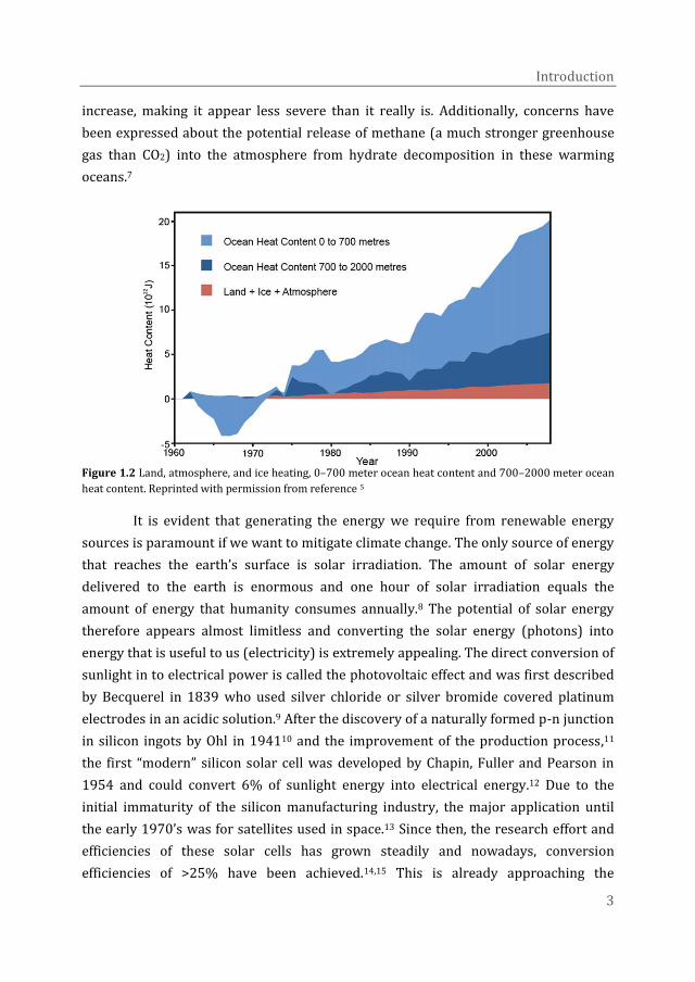
winds (Figure 1.2).4–6 This heat uptake is masking the actual surface temperature
Introduction
3
increase, making it appear less severe than it really is. Additionally, concerns have
been expressed about the potential release of methane (a much stronger greenhouse
gas than CO2) into the atmosphere from hydrate decomposition in these warming
oceans.7
Figure 1.2 Land, atmosphere, and ice heating, 0–700 meter ocean heat content and 700–2000 meter ocean
heat content. Reprinted with permission from reference 5
It is evident that generating the energy we require from renewable energy
sources is paramount if we want to mitigate climate change. The only source of energy
that reaches the earth’s surface is solar irradiation. The amount of solar energy
delivered to the earth is enormous and one hour of solar irradiation equals the
amount of energy that humanity consumes annually.8 The potential of solar energy
therefore appears almost limitless and converting the solar energy (photons) into
energy that is useful to us (electricity) is extremely appealing. The direct conversion of
sunlight in to electrical power is called the photovoltaic effect and was first described
by Becquerel in 1839 who used silver chloride or silver bromide covered platinum
electrodes in an acidic solution.9 After the discovery of a naturally formed p-n junction
in silicon ingots by Ohl in 194110 and the improvement of the production process,11
the first “modern” silicon solar cell was developed by Chapin, Fuller and Pearson in
1954 and could convert 6% of sunlight energy into electrical energy.12 Due to the
initial immaturity of the silicon manufacturing industry, the major application until
the early 1970’s was for satellites used in space.13 Since then, the research effort and
efficiencies of these solar cells has grown steadily and nowadays, conversion
efficiencies of >25% have been achieved.14,15 This is already approaching the
Chapter 1
4
theoretical thermodynamic power conversion efficiency limit in sunlight calculated by
Shockley and Queisser in 1961 of 33.7% for a single p-n junction solar cell with a
bandgap of 1.4 eV.16,17
Nowadays, the crystalline silicon solar cells are completely dominating the
commercial and private photovoltaic (PV) markets. The high production cost of
crystalline silicon solar cells due to the requirement of extremely high purity of raw
materials and high temperature processing has traditionally been used as an
argument for the inability of large scale application of this technology. However, the
upscaling of silicon solar panel production and maturing of the technology has in fact
drastically reduced the production costs in recent years, making it a much more
competitive technology.18 The fact that crystalline silicon is an indirect bandgap
material however requires the semiconductor layer to be relatively thick (~200 µm),
making the panels comparably heavy and making flexible applications nearly
impossible.
Thin film photovoltaics aim to reduce the weight and material cost by
applying a thin active layer (< 5 µm), which is made possible by the use of a direct
bandgap semiconductor absorber. The currently leading thin film PV technologies
include amorphous silicon (a-Si), cadmium telluride (CdTe), copper indium gallium
selenide (CIGS) and gallium arsenide (GaAs) thin film solar cells which have reached
efficiencies of up to 14.0%, 22.1%, 22.6%, and 28.8% respectively.15 The drawback of
these thin film technologies however, is that highest efficiency devices require the use
of highly toxic or very costly materials or production methods. Recently, metal halide
perovskites have emerged as a new thin film PV technology. Promising initial results
and an impressive increase in power conversion efficiency (PCE) in only a few years
have characterized this technology. What is making this thin film technology
potentially so competitive is the combination of solution processability, high efficiency
and low cost.
Introduction
5
1.2 Solar cell operation
The operation of a solar cell relies on the absorption of light and the
subsequent generation and collection of charges. For this purpose, a semiconductor
material is used to form the active layer of the solar cell. Semiconductor materials are
characterized by a bandgap, which is the energy gap that separates the valence band
(VB, the highest energy band occupied by electrons) from the conduction band (CB,
the lowest energy band where no states are occupied). The magnitude of the bandgap
determines which photons can be absorbed by the material, where photons with an
energy less that the bandgap will not be absorbed. When the photon energy is higher
than, or equal to bandgap, an electron is excited from the VB to the CB, and any excess
energy is lost through thermalization. The negatively charged electron (e−) in the CB
leaves behind a positively charged hole (h+) in the VB. In most inorganic
semiconductors the electron and hole can be considered as free charges at room
temperature. When the electron and hole are strongly bound by coulomb interaction,
e.g. due to a low permittivity as commonly found in organic semiconductors, the
electron-hole pair is referred to as an exciton. For a photovoltaic effect the exciton
must be separated into free charges (one e− and one h+) that can move freely through
the active material. After generation and separation, the electrons are collected by an
electrode into an external circuit, where they dissipate energy and produce power
before returning to the solar cell at the opposite electrode, where it recombines with
the hole, closing the cycle. If the electron is not extracted from the solar cell, it will
eventually recombine with the hole and the light generated electron-hole pair and the
accompanying energy are lost.
Chapter 1
6
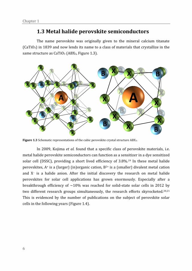
1.3 Metal halide perovskite semiconductors
The name perovskite was originally given to the mineral calcium titanate
(CaTiO3) in 1839 and now lends its name to a class of materials that crystallize in the
same structure as CaTiO3 (ABX3, Figure 1.3).
Figure 1.3 Schematic representations of the cubic perovskite crystal structure ABX3.
In 2009, Kojima et al. found that a specific class of perovskite materials, i.e.
metal halide perovskite semiconductors can function as a sensitizer in a dye sensitized
solar cell (DSSC), providing a short lived efficiency of 3.8%.19 In these metal halide
perovskites, A+ is a (larger) (in)organic cation, B2+ is a (smaller) divalent metal cation
and X− is a halide anion. After the initial discovery the research on metal halide
perovskites for solar cell applications has grown enormously. Especially after a
breakthrough efficiency of ~10% was reached for solid-state solar cells in 2012 by
two different research groups simultaneously, the research efforts skyrocketed.20,21
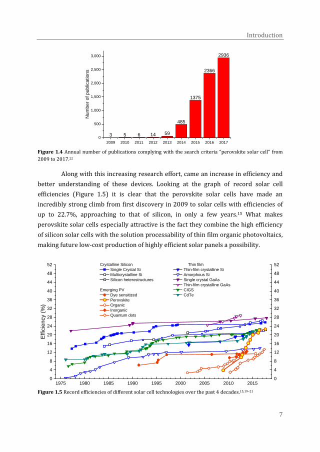
This is evidenced by the number of publications on the subject of perovskite solar
cells in the following years (Figure 1.4).
X
X XBX X XB
X
XX
X
XX
BX
X
X
X
X
X
XBX
A
X
X
XX
X
X
B X
B
XX
X X
X
X X XBX X
XB
X
X
BX X BX
X
BX
X
X
BX
AX
B X
B
X
XB
X
XB
XX
Introduction
7
3 5 6 14 59
485
1375
2366
2936
2009 2010 2011 2012 2013 2014 2015 2016 2017
0
500
1,000
1,500
2,000
2,500
3,000
Nu
mb
er
of
pu
blic
atio
ns
Figure 1.4 Annual number of publications complying with the search criteria “perovskite solar cell” from
2009 to 2017.22
Along with this increasing research effort, came an increase in efficiency and
better understanding of these devices. Looking at the graph of record solar cell
efficiencies (Figure 1.5) it is clear that the perovskite solar cells have made an
incredibly strong climb from first discovery in 2009 to solar cells with efficiencies of
up to 22.7%, approaching to that of silicon, in only a few years.15 What makes
perovskite solar cells especially attractive is the fact they combine the high efficiency
of silicon solar cells with the solution processability of thin film organic photovoltaics,
making future low-cost production of highly efficient solar panels a possibility.
1975 1980 1985 1990 1995 2000 2005 2010 20150
4
8
12
16
20
24
28
32
36
40
44
48
52
0
4
8
12
16
20
24
28
32
36
40
44
48
52
Effic
iency (
%)
Crystalline Silicon Thin film
Single Crystal Si Thin-film crystalline Si
Multicrystalline Si Amorphous Si
Silicon heterostructures Single crystal GaAs
Thin-film crystalline GaAs
Emerging PV CIGS
Dye sensitized CdTe
Perovskite
Organic
Inorganic
Quantum dots
Figure 1.5 Record efficiencies of different solar cell technologies over the past 4 decades.15,19–21

Chapter 1
8
1.4 Metal halide perovskite composition
As described in paragraph 1.3, the perovskites possess an ABX3 crystal
structure (Figure 1.3). Since the discovery of the perovskite structure in 1839, the
material has been investigated extensively and in 1962, the Goldschmidt tolerance
factor was described by Victor M. Goldschmidt.23 This tolerance factor uses the ionic
radii of the atoms in the perovskite structure and can be used to indicate the stability
of a certain perovskite composition. It is defined as:
𝑡 =𝑟A + 𝑟X
√2 (𝑟B + 𝑟X)
with tolerance factor (t), 𝑟𝐴and 𝑟𝐵 the ionic radii of the A and B cations respectively
and 𝑟𝑋 the ionic radius of the anion. The tolerance factor assesses if the A cation can fit
inside the cavities of the BX3 framework. Where a tolerance factor of t = 1 indicates a
perfect fit resulting in the formation of a perfect cubic perovskite structure. For metal
halide perovskites, the perovskite structure is generally formed with calculated
tolerance factors of 0.81 ≥ t ≤ 1.11, although tilting of the BX6 octahedra can occur in
the lower range. In the narrower range of 0.89 ≥ t ≤ 1.00, the cubic perovskite
structure can be expected. If t > 1.1 or t < 0.8, the A site cation is either too large or too
small respectively and the perovskite structure will generally not be formed.24,25 For
metal halide perovskites, alternative methods for the determination of the ionic radii
have been proposed for several reasons. The A cation is often a molecule with a
non-spherical shape and a dipole moment instead of a spherical single atom. Due to
the low decomposition temperatures of the A molecules, processing is often done at
low temperature, which can result in the kinetic trapping of the material in a
thermodynamically less stable state. The tolerance factor equation is designed for use
with oxides and fluorides which can be interpreted as non-polarizable hard spheres,
which might not be valid for the halogen anions used in metal halide
perovskites.24,26,27 Besides the tolerance factor, the stability of the perovskite is also
determined by the octahedral factor µ, which is defined as:
𝜇 =𝑟𝐵
𝑟𝑋
and should lie between 0.44 and 0.90 for stable perovskite structures.24,25,28 The
relatively broad ranges for stable perovskite structures in tolerance factor and
octahedral factor already suggest that the perovskite structure is quite tolerant
towards changes in composition. Consequently, many different compositions of metal
halide perovskites have been produced and studied as will be discussed later.
Introduction
9
In the original publication of Kojima et al. the studied perovskite consisted of
methylammonium (CH3NH3+ (MA+)) as the large organic cation (A+), lead(II) (Pb2+) as
the divalent metal cation (B2+) and iodide (I−) or bromide (Br−) as the halide (X−) and
remains the most extensively studied compositions for use in photovoltaic
applications to date.19 These structures are referred to as methylammonium lead
triiodide (MAPbI3) and methylammonium lead tribromide (MAPbBr3) respectively. In
general, the metal halide perovskite structures used for photovoltaic applications are
considered to be relatively soft and malleable crystal structures. Consequently,
sensitivity of the material to ambient conditions and thermal instability of the
structures have been widely reported.29–32 Additionally, the materials undergo several
phase transitions as a function of a changing temperature.33
One of the main advantages and an attractive aspect of the perovskite
material is its tolerance to the (partial) exchange of one or more of its three
compounds (A, B and X) with different molecules or atoms. This change of the
perovskite composition has been found to influence the materials’ physical properties
significantly and many different compositions have been reported. Potentially
allowing the tuning of the perovskites’ physical properties towards application
specific requirements.
Replacing the large organic cation (A)
In the MAPbI3 composition (bandgap ~1.55 eV), the A cation (MA+) has been
replaced with the larger formamidinium (CH(NH2)2+, FA+), as well as with the smaller
cesium (Cs+) or rubidium (Rb+). Both MA+ and FA+ are organic molecules with a dipole
moment while Cs+ and Rb+ are inorganic atoms without a permanent dipole moment.
The cation size difference causes the lattice to expand (FA+) or contract (Cs+ and Rb+),
changing the B-X bond length and has been found to have a small effect on the
bandgap of the material.34–40 Complete replacement of MA+ with FA+ (FAPbI3) results
in a photo-inactive, yellow non perovskite (δ) phase at room temperature which can
be turned into the dark perovskite (α) phase at elevated temperatures (125 –
165°C).38,41–43 Upon storage at room temperature however, a slow phase transition
back to the δ phase has been reported, making device performance unstable over
time.41,43–47 Mixing FA+ into the MAPbI3 (resulting in a mixed FAxMA1−xPbI3 perovskite)
however, allows a moderate reduction of the bandgap (higher FA+ fraction results in a
lower bandgap) and results in more stable compounds.34,45,46,48 Partial replacement of
MA+ with Cs+ has shown to moderately increase the bandgap of the perovskite and
improve its ambient thermal stability.49,50 Similar to the MAPbI3 case, partially
Chapter 1
10
replacing FA+ with Cs+ in FAPbI3 results in a moderate increase in the bandgap and
increased stability of the formed perovskite.38,39,51–53 The complete replacement of
MA+/FA+ with Cs+, gives CsPbI3 which exhibits polymorphism, similar to FAPbI3, with
a phase transition above 300 °C and also suffers from instability at room temperature
due to a favourable α to δ phase transition at room temperature.49,54 Partial
replacement of FA+ with Rb+ is possible but only with very low fractions of Rb+ before
phase segregation occurs.40,55 With a Rb+ fraction of 0.05 (Rb0.05FA0.95PbI3), the α
perovskite phase is formed around 120 – 150 °C which is stable at room temperature,
while pure RbPbI3 only shows a δ phase that is photo-inactive. Even with only this
small amount of incorporated Rb+, the stability towards moisture exposure at room
temperature is greatly enhanced.40,55 Due to the low Rb+ fraction that can be
incorporated, a change in the bandgap was not observed.40,55
With the mixing of organic cations to form new perovskite structures, a
method for calculating the effective tolerance factor (teff) was proposed which
employs the atomic-ratio weighted average of the two different cations for calculating
the effective ionic radius (reff). With the best performing perovskite devices exhibiting
a teff between teff = 0.94 and teff = 0.98.38
𝑡eff =𝑟eff + 𝑟X
√2(𝑟B + 𝑟X)
𝑟eff = 𝑥𝑟A1+ (1 − 𝑥)𝑟A2
Replacing the halogen ion (X)
The substitution of I− by Cl− in the MAPbI3 composition has been studied
extensively in the earlier years of perovskite solar cell research since it produced the
highest efficiency devices at that time. The incorporation of Cl− into the MAPbI3 crystal
has however been subject of substantial debate. With many studies showing some
degree of Cl− incorporation in the MAPbI structure,56–71 but just as many showing
there is no incorporated Cl− in the final perovskite structure.72–86 This makes it
difficult to ascribe any changes in physical properties to the incorporation of Cl− into
the perovskite structure. The general consensus is however that Cl− incorporation is
very small if any and that the reported changes in the physical properties (like
improved electron and hole diffusion lengths, are related more closely to the changes
in morphology and crystallite quality than to the incorporation of Cl−.34,47,70,87–90
In contrast to the Cl− incorporation, the substitution of I− with Br− in the
MAPbI3 and FAPbI3 structures has been widely demonstrated and compounds have
been produced with values of x ranging from x = 0 to x = 1 in MAPb(I1−xBrx)3 and

Introduction
11
FAPb(I1−xBrx)3.34,91–93 The incorporation of Br− into the MAPbI3 and FAPbI3 allows
modification of the perovskite material bandgap much more effectively than by
changing the organic cation. With increasing Br− content, the bandgap increases as
much as ~0.7 eV and ~0.8 eV for the MA and FA compositions, respectively (versus a
bandgap change of ~0.1 eV for changing the organic A cation) upon complete
substitution of I− with Br−.91–94 With the increasing Br− content up to x > 0.2 an
increase in stability towards moisture exposure has also been reported for
MAPb(I1−xBrx)3.93 Under accelerated stress tests, using extremely strong illumination
conditions (~100 suns), MAPbBr3 turns out to be the most stable composition.95
Although mixed MAPb(I1−xBrx)3 compounds are stable under storage conditions, the
materials phase segregate over time under illumination (1 sun) into iodine-rich and
bromide-rich phases.94–97 This phase segregation has been shown to be reversible by
storage in the dark at room temperature. Additional experiments have shown that this
phase segregation is caused solely by illumination and is not an effect of temperature
increase, nevertheless, the phase segregation rate is strongly temperature
dependent.94,98 By replacing MA+ with Cs+ in the MAPb(I1−xBrx)3 structure, the thermal
and illuminated stability of the material is enhanced and the phase segregation is
minimal for values of x < 0.4. For values of x > 0.4 phase segregation does occur.99,100
Contrary to the MAPb(I/Cl) mixtures, the incorporation of Cl− in MAPb(Br/Cl)
mixtures has been demonstrated and single crystals have been grown for the full
range of MAP(Br1-xClx)3 mixtures.94,101–103 The smaller difference in ionic radius of Cl−
(1.67 Å) and Br− (1.84 Å) versus I− (2.07 Å) is probably the reason for the compatibility
of Cl− with Br− but not with I−.90,104 The bandgap of the MAPb(Br1-xClx)3
mixtures (~2.3 eV – ~3.05 eV) is much larger than that of the MAPb(I1−xClx)3 and
MAPb(I1−xBrx)3 mixtures.103 Due to this high bandgap, the material is less interesting
for PV applications and therefore, most studies on this material focus on light emitting
devices where the emitted color can be tuned from yellow towards blue.103,105–108
Ternary mixtures that contain all three halogen ions described above (I−, Cl−,
and Br−) have also been reported. The results from these studies are very similar to
the ones from the binary mixtures. The Cl− incorporation was found to be minimal
again but does have influence on device performance through improved crystal
quality or morphology. An increase in Br− incorporation again strongly increases the
bandgap of the material and improves the stability of the formed compound.109–111
Chapter 1
12
Replacing the divalent metal cation (B)
The main reason for replacing the divalent metal cation lead(II) (Pb2+) in
metal halide perovskites is to reduce the materials’ toxicity. The ionic radius of the
less toxic tin(II) (Sn2+, 1.35Å) is similar to that of Pb2+ (1.49Å) and complete
substitution of Pb2+ with Sn2+ in the MAPbI3 compound has been accomplished.109–111
The formed compound turns to dark perovskite at room temperature and this
complete substitution reduces the bandgap to ~1.3 eV.112,113 The complete
substitution of Pb2+ with Sn2+ in the FAPbI3 compound has also been achieved,
resulting in a perovskite phase with no known polymorphs and a reduction in the
bandgap from 1.48 eV (FAPbI3) to 1,41 eV (FASnI3).112,114
A disadvantage of the substitution of Pb2+ with Sn2+ in perovskite
compositions is that Sn2+ oxidizes easily to Sn4+, whereby the perovskite structure and
its functionality are lost.113,115–117 Moreover, at least up to now, the efficiency of Sn2+
based perovskite solar cells has been less than that of Pb2+ based devices.113,115,117–119
As in the MAPbI3 case, the bandgap of the tin based perovskite can also be
tuned by the partial substitution of I− by Br− (MASn(I1−xBrx)3) where bandgaps
between 1.3 eV (x = 0) and 2.15 eV (x = 1) can be reached, where again the efficiency
lacks considerably compared to its lead based counterpart.112
Mixtures of Pb2+ and Sn2+ (MASn1−xPbxI3) have also been produced where
interestingly the calculated bandgap of the mixture is smaller than that of both
pristine compounds for values of x < 0.8.120–122
Theoretical calculations show that Pb2+ can also be replaced with germanium
(Ge2+) and provide stable compounds. The ionic radius of Ge2+ is smaller than that of
Sn2+ and Pb2+ and with an increasing ionic radius of the A cation (Cs < MA < FA) the
bandgap of the Ge2+-based perovskites increases (1.63 eV for CsGeI3, 2.0 eV for MAGeI3
and 2.35 eV for FAGeI3), which is opposite to the results of its lead counterpart.118 So
far, the efficiency of Ge2+ based perovskite solar cells is very low and as with Sn2+, Ge2+
is easily oxidized to Ge4+ whereby the perovskite structure and its functional
properties are lost.119,123
Perovskite materials in which Pb2+ has been substituted with magnesium
(Mg), thallium (Tl) in combination with bismuth (Bi), sulfur (S) and selenium (Se)
have also been investigated. These structures have however only resulted in devices
with very low efficiencies (< 1%) and some of these compounds are even more toxic
than the lead they replace, invalidating the original purpose of the lead
replacement.118,119
Introduction
13
In the search for a lead(II) substitute in perovskite materials to reduce or
even completely eliminate their toxicity, Sn2+ and Ge2+ seem the most likely candidate
to date. However, the low efficiency of the devices and instability of the perovskite due
to the oxidation of the Sn2+ to Sn4+ and Ge2+ to Ge4+ limits the implementation of these
materials.
Complex mixtures
More complex mixtures containing multiple cations in combination with
multiple halogens have also been used often. As a matter of fact the best performing
devices (in efficiency as well as stability) are currently being produced using these
highly complex mixtures.42,124,125 Since the physical properties of these mixtures are
altered in a multitude of ways simultaneously, it is challenging to ascribe them to
anything specific. Although, it can be expected that substitution of the cation or
halogen will have a similar effect in these complex mixtures as they do in the binary
and ternary mixtures.
1.5 Perovskite solar cell architectures and
processing methods
For the fabrication of solid state perovskite solar cells, mainly four different
solar cell architectures are used. These architectures are termed mesoporous,
capping-layer, planar n-i-p and planar p-i-n. Examples of these four are displayed in
Figure 1.6. The mesoporous perovskite solar cell is a remainder of its first use as a
sensitizer in a dye sensitized solar cells (DSSC). On top of the glass substrate and
transparent electrode a compact electron transport layer (ETL), usually TiO2, is
deposited. On top of this, a mesoporous ETL (usually TiO2 or Al2O3) is produced by
sintering small particles together at high temperature (>400 °C). This porous
mesoscopic structure is then filled with the perovskite active layer on top of which the
solid hole transport layer (HTL), usually doped 2,2',7,7'-tetrakis-(N,N-di-4-
methoxyphenylamino)-9,9'-spirobifluorene (Spiro-OMeTAD), and an opaque back
contact (usually gold (Au)) are deposited (Figure 1.6a). From this mesoscopic
configuration, the capping-layer structure has evolved. Since it was found that the
perovskite does not need the ETL/perovskite interface to separate photo-generated
excitons into free charges and the perovskite material is capable of efficient ambipolar
charge transport, the thickness of the mesoscopic structure was significantly reduced
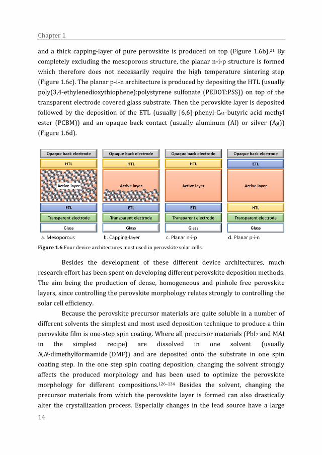
Chapter 1
14
and a thick capping-layer of pure perovskite is produced on top (Figure 1.6b).21 By
completely excluding the mesoporous structure, the planar n-i-p structure is formed
which therefore does not necessarily require the high temperature sintering step
(Figure 1.6c). The planar p-i-n architecture is produced by depositing the HTL (usually
poly(3,4-ethylenedioxythiophene):polystyrene sulfonate (PEDOT:PSS)) on top of the
transparent electrode covered glass substrate. Then the perovskite layer is deposited
followed by the deposition of the ETL (usually [6,6]-phenyl-C61-butyric acid methyl
ester (PCBM)) and an opaque back contact (usually aluminum (Al) or silver (Ag))
(Figure 1.6d).
Figure 1.6 Four device architectures most used in perovskite solar cells.
Besides the development of these different device architectures, much
research effort has been spent on developing different perovskite deposition methods.
The aim being the production of dense, homogeneous and pinhole free perovskite
layers, since controlling the perovskite morphology relates strongly to controlling the
solar cell efficiency.
Because the perovskite precursor materials are quite soluble in a number of
different solvents the simplest and most used deposition technique to produce a thin
perovskite film is one-step spin coating. Where all precursor materials (PbI2 and MAI
in the simplest recipe) are dissolved in one solvent (usually
N,N-dimethylformamide (DMF)) and are deposited onto the substrate in one spin
coating step. In the one step spin coating deposition, changing the solvent strongly
affects the produced morphology and has been used to optimize the perovskite
morphology for different compositions.126–134 Besides the solvent, changing the
precursor materials from which the perovskite layer is formed can also drastically
alter the crystallization process. Especially changes in the lead source have a large
Introduction
15
effect on the crystallization kinetics. It has been shown that (partial) replacement of
lead(II) iodide (PbI2) with lead(II) chloride (PbCl2) retards the crystallization process,
allowing the perovskites crystallites to grow bigger, while (partial) replacement of
PbI2 with lead(II) acetate (Pb(OAc)2) speeds up the crystallization process.135–139 The
chloride and acetate do however not incorporate into the perovskite structure like Br
does; they mainly affect the crystallization speed and are released out of the
perovskite along with the excess organics.59,62,65,73,77,78 An excess of one of the
precursor materials in the mixture or the addition of an acid or inert filler is also often
used to influence the morphology and conversion of the perovskite layer.91,125,140–148
Application of an anti-solvent on top of the wet perovskite film during spin coating
drives away the excess solvent, forcing fast nucleation and crystallization to
happen.133,149–152
In order to gain more control of the crystallization process, the crystallization
of PbI2 and conversion to the perovskite material can be separated by sequential
processing. With this method the lead precursor is usually deposited first by spin
coating and converted into perovskite by exposure of the formed (PbI2) film to the
organic compound (usually MAI). Where deposition of the PbI2 from DMF results in
crystalline layers, deposition from the strongly coordinating solvents e.g. dimethyl
sulfoxide (DMSO) results in amorphous PbI2 layers.128,133,153–159 This PbI2 layer can
also be thermally or solvent annealed to optimize its morphology for incorporation of
the organic compound in the second processing step.157,158,160–164 The organic
compound can be introduced to the completed PbI2 layer in a variety of ways. A
solution containing the organic compound can be spin coated on top of the PbI2
covered substrate,159,162–167 the PbI2 covered substrate can be immersed into a MAI (or
MAI/MACl) containing solution (usually in 2-propanol).67,73,128,157,158,160,161,168–172 For
these two-step deposition techniques, two competing crystallization mechanisms
have been proposed as the conversion process. The first being in-situ conversion,
where the organic compound incorporates into the PbI2 crystals and the morphology
formed in the first step remains and the second being dissolution-recrystallization,
where the PbI2 layer (partially) dissolves in the solvent used in the second step and
the perovskite material crystallizes forming a new morphology.173,174 All the solution
processed films usually require some post deposition thermal annealing to evaporate
solvent and promote crystallization. A great variety of annealing schemes has been
proposed in the search for the most efficient devices including solvent annealing,
exposure to moisture and methods that eliminate thermal annealing
altogether.72,139,175–183
Chapter 1
16
The organic compound can also be supplied from the vapor phase, which can
be done using expensive high vacuum equipment but can also be done in cheaper and
simpler low vacuum or atmospheric conditions.184–187 Completely thermally
evaporated perovskite films have also been produced in which different techniques
have also been used.187–191 Using co-evaporation it is challenging to keep the
evaporation rate of both materials constant to avoid inhomogeneity in the perovskite
layer. (Co-) evaporation could however potentially allow the production of perovskite
layers with gradual changes in doping level or composition. Single crystals of different
perovskite materials have also been fabricated, often using the inverse thermal
solubility that some perovskite precursor-solvent combinations exhibit.192–194 Some
large area deposition techniques that have been explored successfully include doctor
blading, roll to roll processing, slot dye coating, soft cover deposition and press-peel
techniques.41,195–200
Throughout the development of ever more efficient perovskite solar cells, it
appears like the efficiency increases when the perovskite composition and production
procedure become more and more complex. Illustrated by the two published highest
efficiency perovskite solar cells (22.1% and 21.1%, respectively) that are currently
being produced as follows. In the first, the precursor solution consists of PbI2 and
PbBr2 in a mixture of DMF and DMSO, which is deposited onto mesoporous TiO2 on
top of a compact TiO2 layer on fluorinated tin oxide (FTO). A mixture of FAI, and MABr
in 2-propanol (IPA) containing hydrogen triiodide is then spin coated onto the wet
layer after which the perovskite layer is annealed. After this, the perovskite layers is
washed with pure IPA and annealed again. A doped poly(triaryl amine) (PTAA)
semiconductor layer is deposited as HTL and a gold electrode completes the device.124
In the second, the precursor solution consists of FAI, PbI2, MABr, PbBr2 and CsI in a
mixture of DMF and DMSO, which is deposited onto doped mesoporous TiO2 on top of
a compact TiO2 layer on FTO. During spin coating, the anti-solvent chlorobenzene is
deposited on top of the still wet film. A doped Spiro-OMeTAD layer is deposited as
HTL and a gold electrode completes the device.42
The perovskite solar cells produced for the work described in this thesis have
a planar p-i-n architecture, with a device stack consisting of a patterned indium tin
oxide (ITO) transparent electrode on top of a glass slide. On top of which the
PEDOT:PSS HTL is deposited. A MAPbI3 perovskite material is deposited on top and
the devices are completed by application of a PCBM ETL and a LiF/Al top contact.
Introduction
17
1.6 Advantages and challenges
Beyond doubt, the perovskite material is suitable for use as an active material
in solar cells. The high absorption coefficient, low exciton binding energy and efficient
ambipolar charge transport capabilities of the material make the production of highly
efficient thin film devices possible. Due to the high solubility of the precursor
materials, low cost solution processing of the perovskite layer is an attractive option.
Even though the record efficiency of perovskite solar cells is approaching that of the
industry giant silicon, the price of silicon solar panels has dropped so significantly due
to the development and maturing of the fabrication processes, that the low material
costs of perovskite solar cells is no longer a strong selling point for the technology.
The high defect tolerance and ability to change the composition of the material and
with that tune its physical properties towards specific applications is however a
unique advantage of perovskite materials. Combining this with the large number of
diverse processing methods that have been developed, the way is paved for
application of perovskite solar cells in large area applications as well as niche markets
like flexible and tandem solar cells. The main challenges that remain for the
technology are the toxicity of the lead that is used in the material. Although
calculations and studies have shown that the amount of lead in perovskite solar panels
is far from catastrophic for the environment or the public, recycling seems a viable
option and alternatives like tin might be more toxic to the aquatic environment than
lead, avoiding possible exposure to toxic materials is always preferable.201–207
Furthermore, the long term stability of the material under operating conditions still
deserves attention.

Chapter 1
18
1.7 Aim and outline of this thesis
The research described in this thesis aims to introduce the perovskite
material as a semiconductor for solar cell applications within the research group.
Furthermore, the aim is to optimize the device performance and gain a better
understanding of the material properties and photophysical processes inside the
perovskite solar cells.
The correct characterization of perovskite solar cells can be challenging due
to the typical response these cells can have towards the traditional measurement
protocols. Especially sub-optimal perovskite solar cells can show misleading results in
efficiency measurements. Therefore, measurement protocols specifically for
perovskite solar cells were developed which provide correct and reliable data. The
development process of these measurement protocols and the response of the
perovskite solar cells towards these and the traditional measurement protocols are
discussed in Chapter 2 of this thesis.
Chapter 3 describes the use of different perovskite precursor materials and
the effect they have on the perovskite layer morphology. When using PbCl2 as the only
lead source in combination with MAI dissolved in DMF, the resulting perovskite layers
are rough and show large voids in between the perovskite crystals. By combining
PbCl2 and Pb(OAc)2 as the lead source, the ration between the two can be used to
finely tune the layer morphology and improve the device performance. Further
optimization of the production procedure resulted in the reproducible production of
solar cells with a PCE of ~14%.
In Chapter 4 the influence of the processing atmosphere on the optimized
perovskite solar cell performance is described. It was found that the influence of the
atmosphere during spin coating is negligible, while the influence of the atmosphere
during annealing is critical. Further investigation shows that it is specifically exposure
to oxygen (O2) during annealing that is crucial for high efficiency devices. This is
because the application of the perovskite precursor solution on top of the poly(3,4-
ethylenedioxythiophene):polystyrene sulfonate (PEDOT:PSS) HTL chemically reduces
the oxidation state of the HTL. This changes the work function of the PEDOT:PSS that
in turn alters that of the perovskite layer on top of it, resulting in lower efficiency solar
cells, mainly due to reductions in open-circuit voltage and short-circuit current
density. The exposure to O2 during the annealing step (partially) re-oxidizes the
PEDOT:PSS, restoring its function in the solar cell and yielding highly efficiency
devices.
Introduction
19
In chapter 5, a sequential deposition method is introduced, in which a layer of
the metal halide (PbI2) is spin coated first, that is converted into perovskite
subsequently by introducing the organic compound (MAI) from the vapor phase. This
method has been termed vapor assisted solution processing (VASP) in literature. In
this chapter, initial experiments using a commercial thermal gradient sublimer
confirm the possibility of conversion of PbI2 layers into perovskite layers with this
method. After determining the most critical parameters in the deposition process,
using this setup, a dedicated VASP reactor is designed and built. This reactor provides
more control over the parameters that were found highly influential in the deposition
process. Experiments in which the deposition profile of MAI onto glass slides is
assessed show that the carrier gas flow rate strongly influences the homogeneity of
the deposition profile, while the temperature (difference) of the crucible and sample
stage mainly determine the amount of deposition. When converting PbI2 layers on
glass slides, it is found that a proper balance between the deposition and the
conversion reaction is much more important than heavy MAI deposition. Finally when
producing solar cells using this sequential deposition method, it is found that the flow
rate of the heated carrier gas is crucial for obtaining decent perovskite layers for
application in a solar cell. A low flow rate is essential for gentle MAI deposition and
providing sufficient time for the conversion reaction to occur. Furthermore, it is found
that the purity of the PbI2 that is used has a significant influence on the conversion
and therefore the solar cell performance. The highest solar cell efficiency that was
achieved using this equipment is 11.7%.

Chapter 1
20
1.8 References
1 EIA, U.S. Energy Inf. Adm., 2017, IEO2017.
2 Bloomberg, What’s Really Warming the World,
https://www.bloomberg.com/graphics/2015-whats-warming-the-world/, (accessed 3
January 2018).
3 R. L. Miller, G. A. Schmidt, L. S. Nazarenko, N. Tausnev, S. E. Bauer, A. D. DelGenio, M.
Kelley, K. K. Lo, R. Ruedy, D. T. Shindell, I. Aleinov, M. Bauer, R. Bleck, V. Canuto, Y.
Chen, Y. Cheng, T. L. Clune, G. Faluvegi, J. E. Hansen, R. J. Healy, N. Y. Kiang, D. Koch, A.
A. Lacis, A. N. LeGrande, J. Lerner, S. Menon, V. Oinas, C. Pérez García-Pando, J. P.
Perlwitz, M. J. Puma, D. Rind, A. Romanou, G. L. Russell, M Sato, S Sun, K. Tsigaridis, N.
Unger, A. Voulgarakis, M.-S. Yao, and J. Zhang, J. Adv. Model. Earth Syst., 2014, 6, 441–
477.
4 M. H. England, S. Mcgregor, P. Spence, G. A. Meehl, A. Timmermann, W. Cai, A. S. Gupta,
M. J. McPhaden, A. Purich and A. Santoso, Nat. Clim. Chang., 2014, 4, 222–227.
5 D. Nuccitelli, R. Way, R. Painting, J. Church and J. Cook, Phys. Lett. A, 2012, 376, 3466–
3468.
6 D. H. Douglass and R. S. Knox, Phys. Lett. A, 2012, 376, 3673–3675.
7 S. L. Hautala, E. A. Solomon, H. P. Johnson, R. N. Harris and U. K. Miller, Geophys. Res.
Lett., 2014, 41, 8486–8494.
8 G. W. Crabtree and N. S. Lewis, Phys. Today, 2007, 60, 37.
9 A. E. Becquerel, Comptes Rendus L´Academie des Sciences, 1839, 9, 145–149.
10 R. S. Ohl, US patent, 1941, 2, 402, 602.
11 R. S. Ohl and E. F. Kingsburry, Bell Syst. Tech. J., 1952, 31, 802–815.
12 D. M. Chapin, C. S. Fuller and G. L. Pearson, J. Appl. Phys., 1954, 25, 676–677.
13 C. Honsberg and S. Bowden, Early silicon solar cells,
http://www.pveducation.org/pvcdrom/manufacturing/early-silicon-solar-cells,
(accessed 3 January 2018).
14 Fraunhofer ISE, Press-release, Fraunhofer ISE Achieves New World Record for Both
Sides-Contacted Silicon Solar Cells, Freiburg, 2015.
https://www.ise.fraunhofer.de/en/press-media/press-releases/2015/fraunhofer-ise-
achieves-new-world-record-for-both-sides-contacted-silicon-solar-cells.html
(accessed 30 January 2018)
15 National Renewable Energy Laboratory, NREL efficiency chart,
https://www.nrel.gov/pv/assets/images/efficiency-chart.png, (accessed 3 January
2018).
16 W. Shockley and H. J. Queisser, J. Appl. Phys., 1961, 32, 510–519.
17 S. Rühle, Sol. Energy, 2016, 130, 139–147.

Introduction
21
18 Fraunhofer ISE (2015): Current and Future Cost of Photovoltaics. Long-term Scenarios
for Market Development, System Prices and LCOE of Utility-Scale PV Systems. Study on
behalf of Agora Energiewende
19 A. Kojima, K. Teshima, Y. Shirai and T. Miyasaka, J. Am. Chem. Soc., 2009, 131, 6050–
6051.
20 H.-S. Kim, C.-R. Lee, J.-H. Im, K.-B. Lee, T. Moehl, A. Marchioro, S.-J. Moon, R. Humphry-
Baker, J.-H. Yum, J. E. Moser, M. Grätzel and N.-G. Park, Sci. Rep., 2012, 2, 591.
21 M. M. Lee, J. Teuscher, T. Miyasaka, T. N. Murakami and H. J. Snaith, Science, 2012, 338,
643–647.
22 Web of Science, Annual number of publications,
https://apps.webofknowledge.com/RAMore.do?product=WOS&search_mode=General
Search&SID=E1rYWp3nndHncVdBATq&qid=1&ra_mode=more&ra_name=Publication
Year&colName=WOS&viewType=raMore&more_sort_order=alpha, (accessed 3
January 2018).
23 V. M. Goldschmidt, Naturwissenschaften, 1926, 14, 477–485.
24 W. Travis, E. N. K. Glover, H. Bronstein, D. O. Scanlon and R. G. Palgrave, Chem. Sci.,
2016, 7, 4548–4556.
25 M. A. Green, A. Ho-Baillie and H. J. Snaith, Nat. Photonics, 2014, 8, 506–514.
26 G. Kieslich, S. Sun and A. K. Cheetham, Chem. Sci., 2014, 5, 4712–4715.
27 G. Kieslich, S. Sun and A. K. Cheetham, Chem. Sci., 2015, 6, 3430–3433.
28 N. Ashurov, B. L. Oksengendler, S. Maksimov, S. Rashiodva, A. R. Ishteev, D. S. Saranin, I.
N. Burmistrov, D. V. Kuznetsov and A. A. Zakhisov, Mod. Electron. Mater., 2017, 3, 1–25.
29 D. Wang, M. Wright, N. K. Elumalai and A. Uddin, Sol. Energy Mater. Sol. Cells, 2016,
147, 255–275.
30 M. I. Asghar, J. Zhang, H. Wang and P. D. Lund, Renew. Sustain. Energy Rev., 2017, 77,
131–146.
31 T. A. Berhe, W.-N. Su, C.-H. Chen, C.-J. Pan, J.-H. Cheng, H.-M. Chen, M.-C. Tsai, L.-Y. Chen,
A. A. Dubale and B.-J. Hwang, Energy Environ. Sci., 2016, 9, 323–356.
32 W. R. Mateker and M. D. McGehee, Adv. Mater., 2017, 29, 1603940
33 A. M. A. Leguy, A. R. Goñi, J. M. Frost, J. Skelton, F. Brivio, X. Rodríguez-Martínez, O. J.
Weber, A. Pallipurath, M. I. Alonso, M. Campoy-Quiles, M. T. Weller, J. Nelson, A. Walsh
and P. R. F. Barnes, Phys. Chem. Chem. Phys., 2016, 18, 27051–27066.
34 L. K. Ono, E. J. Juarez-Perez and Y. Qi, ACS Appl. Mater. Interfaces, 2017, 9, 30197-30246
35 J.-P. Correa-Baena, A. Abate, M. Saliba, W. Tress, T. Jesper Jacobsson, M. Grätzel and A.
Hagfeldt, Energy Environ. Sci., 2017, 10, 710–727.
36 N. Pellet, P. Gao, G. Gregori, T.-Y. Yang, M. K. Nazeeruddin, J. Maier and M. Grätzel,
Angew. Chemie - Int. Ed., 2014, 53, 3151–3157.
37 H. Choi, J. Jeong, H.-B. Kim, S. Kim, B. Walker, G.-H. Kim and J. Y. Kim, Nano Energy,
2014, 7, 80–85.
Chapter 1
22
38 Z. Li, M. Yang, J.-S. Park, S.-H. Wei, J. J. Berry and K. Zhu, Chem. Mater., 2016, 28, 284–
292.
39 J.-W. Lee, D.-H. Kim, H.-S. Kim, S.-W. Seo, S. M. Cho and N.-G. Park, Adv. Energy Mater.,
2015, 5, 1501310.
40 Y. H. Park, I. Jeong, S. Bae, H. J. Son, P. Lee, J. Lee, C.-H. Lee and M. J. Ko, Adv. Funct.
Mater., 2017, 27, 1605988.
41 Y. Deng, Q. Dong, C. Bi, Y. Yuan and J. Huang, Adv. Energy Mater., 2016, 6, 1600372.
42 M. Saliba, T. Matsui, J.-Y. Seo, K. Domanski, J.-P. Correa-Baena, M. K. Nazeeruddin, S. M.
Zakeeruddin, W. Tress, A. Abate, A. Hagfeldt and M. Grätzel, Energy Environ. Sci., 2016,
9, 1989–1997.
43 C. C. Stoumpos, C. D. Malliakas and M. G. Kanatzidis, Inorg. Chem., 2013, 52, 9019–
9038.
44 A. Binek, F. C. Hanusch, P. Docampo and T. Bein, J. Phys. Chem. Lett., 2015, 6, 1249–
1253.
45 B. Slimi, M. Mollar, I. B. Assaker, I. Kriaa, R. Chtourou and B. Marí, Energy Procedia,
2016, 102, 87–95.
46 J. Dai, Y. Fu, L. H. Manger, M. T. Rea, L. Hwang, R. H. Goldsmith and S. Jin, J.-Phys. Chem.
Lett., 2016, 7, 5036-5043.
47 Y. Zhou, Z. Zhou, M. Chen, Y. Zong, J. Huang, S. Pang and N. P. Padture, J. Mater. Chem. A,
2016, 4, 17623–17635.
48 O. J. Weber, B. Charles and M. T. Weller, J. Mater. Chem. A, 2016, 4, 15375–15382.
49 G. E. Eperon, G. M. Paternò, R. J. Sutton, A. Zampetti, A. A. Haghighirad, F. Cacialli and H.
J. Snaith, J. Mater. Chem. A, 2015, 3, 19688–19695.
50 G. Niu, W. Li, J. Li, X. Liang and L. Wang, RSC Adv., 2017, 7, 17473–17479.
51 J. Huang, P. Xu, J. Liu and X. Z. You, Small, 2017, 13, 1603225.
52 T. Liu, Y. Zong, Y. Zhou, M. Yang, Z. Li, O. S. Game, K. Zhu, R. Zhu, Q. Gong and N. P.
Padture, Chem. Mater., 2017, 29, 3246–3250.
53 Y. Yu, C. Wang, C. R. Grice, N. Shrestha, J. Chen, D. Zhao, W. Liao, A. J. Cimaroli, P. J.
Roland, R. J. Ellingson and Y. Yan, ChemSusChem, 2016, 9, 3288–3297.
54 M. C. Neuburger, Z. Kristallogr., 1936, 93, 314
55 M. Zhang, J. S. Yun, Q. Ma, J. Zheng, C. F. J. Lau, X. Deng, J. Kim, D. Kim, J. Seidel, M. A.
Green, S. Huang and A. W. Y. Ho-Baillie, ACS Energy Lett., 2017, 2, 438–444.
56 S. Colella, E. Mosconi, P. Fedeli, A. Listorti, F. Gazza, F. Orlandi, P. Ferro, T. Besagni, A.
Rizzo, G. Calestani, G. Gigli, F. De Angelis and R. Mosca, Chem. Mater., 2013, 25, 4613–
4618.
57 B. Conings, L. Baeten, C. De Dobbelaere, J. D’Haen, J. Manca and H. G. Boyen, Adv. Mater.,
2014, 26, 2041–2046.
58 J. You, Z. Hong, Y. Yang, Q. Chen, M. Cai, T.-B. Song and C.-Chen, S. Lu, Y. Liu, H. Zhou and
Y. Yang, ACS Nano, 2014, 8, 1674–1680.
Introduction
23
59 H. Yu, F. Wang, F. Xie, W. Li, J. Chen and N. Zhao, Adv. Funct. Mater., 2014, 24, 7102–
7108.
60 N. Yantara, F. Yanan, C. Shi, H. A. Dewi, P. P. Boix, S. G. Mhaisalkar and N. Mathews,
Chem. Mater., 2015, 27, 2309–2314.
61 P. Pistor, J. Borchert, W. Fränzel, R. Csuk and R. Scheer, J. Phys. Chem. Lett., 2014, 5,
3308–3312.
62 S. Colella, E. Mosconi, G. Pellegrino, A. Alberti, V. L. P. Guerra, S. Masi, A. Listorti, A.
Rizzo, G. G. Condorelli, F. De Angelis and G. Gigli, J. Phys. Chem. Lett., 2014, 5, 3532–
3538.
63 Y. Chen, T. Chen and L. Dai, Adv. Mater., 2015, 27, 1053–1059.
64 E. L. Unger, A. R. Bowring, C. J. Tassone, V. L. Pool, A. Gold-Parker, R. Cheacharoen, K. H.
Stone, E. T. Hoke, M. F. Toney and M. D. McGehee, Chem. Mater., 2014, 26, 7158–7165.
65 Q. Chen, H. Zhou, Y. Fang, A. Z. Stieg, T.-B. Song, H.-H. Wang, X. Xu, Y. Liu, S. Lu, J. You, P.
Sun, J. McKay, M. S. Goorsky and Y. Yang, Nat. Commun., 2015, 6, 7269.
66 D. E. Starr, G. Sadoughi, E. Handick, R. G. Wilks, J. H. Alsmeier, L. Köhler, M. Gorgoi, H. J.
Snaith and M. Bär, Energy Environ. Sci., 2015, 8, 1609–1615.
67 Y. Li, W. Sun, W. Yan, S. Ye, H. Peng, Z. Liu, Z. Bian and C. Huang, Adv. Funct. Mater.,
2015, 25, 4867–4873.
68 L. Cojocaru, S. Uchida, A. K. Jena, T. Miyasaka, J. Nakazaki, T. Kubo and H. Segawa, Chem.
Lett., 2015, 44, 1089–1091.
69 J. Chae, Q. Dong, J. Huang and A. Centrone, Nano Lett., 2015, 15, 8114–8121.
70 V. L. Pool, A. Gold-Parker, M. D. McGehee and M. F. Toney, Chem. Mater., 2015, 27,
7240–7243.
71 M. Ralaiarisoa, Y. Busby, J. Frisch, I. Salzmann, J.-J. Pireaux and N. Koch, Phys. Chem.
Chem. Phys., 2017, 19, 828–836.
72 A. Dualeh, N. Tétreault, T. Moehl, P. Gao, M. K. Nazeeruddin and M. Grätzel, Adv. Funct.
Mater., 2014, 24, 3250–3258.
73 P. Docampo, F. C. Hanusch, S. D. Stranks, M. Döblinger, J. M. Feckl, M. Ehrensperger, N.
K. Minar, M. B. Johnston, H. J. Snaith and T. Bein, Adv. Energy Mater., 2014, 4, 1400355.
74 Y. Zhao and K. Zhu, J. Phys. Chem. C, 2014, 118, 9412–9418.
75 B.-W. Park, B. Philippe and T. Gustafsson, K. Sveinbjörnsson, A Hagfeldt, E. M. J.
Johansson and G. Boschloo, Chem. Mater., 2014, 26, 4466-4471.
76 Y. Tidhar, E. Edri, H. Weissman, D. Zohar, G. Hodes, D. Cahen, B. Rybtchinski and S.
Kirmayer, J. Am. Chem. Soc., 2014, 136, 13249-13256.
77 S. T. Williams, F. Zuo, C.-C. Chueh, C.-Y. Liao, P.-W. Liang and A. K.-Y. Jen, ACS Nano,
2014, 8, 10640–10654.
78 M. I. Dar, N. Arora, P. Gao, S. Ahmad, M. Grätzel and M. K. Nazeeruddin, Nano Lett.,
2014, 14, 6991–6996.
79 F. X. Xie, D. Zhang, H. Su, X. Ren, K. S. Wong, M. Grätzel and W. C. H. Choy, ACS Nano,
2015, 9, 639–646.
Chapter 1
24
80 P. Luo, Z. Liu, W. Xia, C. Yuan, J. Cheng, C. Xu and Y. Lu, J. Mater. Chem. A, 2015, 3,
22949–22959.
81 T.-W. Ng, C.-Y. Chan, M.-F. Lo, Z. Q. Guan and C.-S. Lee, J. Mater. Chem. A, 2015, 3, 9081–
9085.
82 A. Binek, I. Grill, N. Huber, K. Peters, A. G. Hufnagel, M. Handloser, P. Docampo, A.
Hartschuh and T. Bein, Chem. Asian J., 2016, 11, 1199–1204.
83 B. Yang, J. Keum, O. S. Ovchinnikova, A. Belianinov, S. Chen, M.-H. Du, I. N. Ivanov, C. M.
Rouleau, D. B. Geohegan and K. Xiao, J. Am. Chem. Soc., 2016, 138, 5028–5035.
84 X. Zhang, C. Liu, Y. Ma, Y. Shen, H. Li, R. Chen and Y. Mai, Sol. Energy, 2017, 148, 70–77.
85 L. Fan, Y. Ding, J. Luo, B. Shi, X. Yao, C. Wei, D. Zhang, G. Wang, Y. Sheng, Y. Chen, A.
Hagfeldt, Y. Zhao and X. Zhang, J. Mater. Chem. A, 2017, 5, 7423–7432.
86 M. Jiang, J. Wu, F. Lan, Q. Tao, D. Gao and G. Li, J. Mater. Chem. A, 2015, 3, 963–967.
87 S. D. Stranks, G. E. Eperon, G. Grancini, C. Menelaou, M. J. P. Alcocer, T. Leijtens, L. M.
Herz, A. Petrozza and H. J. Snaith, Science, 2013, 342, 341–344.
88 G. Xing, N. Mathews, S. Sun, S. S. Lim, Y. M. Lam, M. Grätzel, S. Mhaisalkar, T. C. Sum,
Science, 2013, 342, 344–347.
89 W.-J. Yin, J.-H. Yang, J. Kang, Y. Yan and S.-H. Wei, J. Mater. Chem. A, 2015, 3, 8926–8942.
90 Q. Chen, N. De Marco, Y. Yang, T.-B. Song, C.-C. Chen, H. Zhao, Z. Hong, H. Zhou and Y.
Yang, Nano Today, 2015, 10, 355–396.
91 G. E. Eperon, S. D. Stranks, C. Menelaou, M. B. Johnston, L. M. Herz and H. J. Snaith,
Energy Environ. Sci., 2014, 7, 982.
92 P. Fedeli, F. Gazza, D. Calestani, P. Ferro, T. Besagni, A. Zappettini, G. Calestani, E.
Marchi, P. Ceroni and R. Mosca, J. Phys. Chem. C, 2015, 119, 21304–21313.
93 J. H. Noh, S. H. Im, J. H. Heo, T. N. Mandal and S. Il Seok, Nano Lett., 2013, 13, 1764–
1769.
94 E. T. Hoke, D. J. Slotcavage, E. R. Dohner, A. R. Bowring, H. I. Karunadasa and M. D.
McGehee, Chem. Sci., 2015, 6, 613–617.
95 R. K. Misra, L. Ciammaruchi, S. Aharon, D. Mogilyansky, L. Etgar, I. Visoly-Fisher and E.
A. Katz, ChemSusChem, 2016, 9, 2572–2577.
96 C. G. Bischak, C. L. Hetherington, H. Wu, S. Aloni, D. F. Ogletree, D. T. Limmer and N. S.
Ginsberg, Nano Lett., 2017, 17, 1028–1033.
97 Y. Yuan and J. Huang, Acc. Chem. Res., 2016, 49, 286–293.
98 F. Brivio, C. Caetano and A. Walsh, J. Phys. Chem. Lett., 2016, 7, 1083–1087.
99 R. E. Beal, D. J. Slotcavage, T. Leijtens, A. R. Bowring, R. A. Belisle, W. H. Nguyen, G. F.
Burkhard, E. T. Hoke and M. D. McGehee, J. Phys. Chem. Lett., 2016, 7, 746–751.
100 R. J. Sutton, G. E. Eperon, L. Miranda, E. S. Parrott, B. A. Kamino, J. B. Patel, M. T.
Hörantner, M. B. Johnston, A. A. Haghighirad, D. T. Moore and H. J. Snaith, Adv. Energy
Mater., 2016, 6, 1502458.
101 N. Kitazawa, Y. Watanabe and Y. Nakamura, J. Mater. Sci., 2002, 37, 3585–3587.
Introduction
25
102 T. Zhang, M. Yang, E. E. Benson, Z. Li, J. van de Lagemaat, J. M. Luther, Y. Yan, K. Zhu and
Y. Zhao, Chem. Commun., 2015, 51, 7820–7823.
103 Y. Fang, Q. Dong, Y. Shao, Y. Yuan and J. Huang, Nat. Photonics, 2015, 9, 679–686.
104 W.-J. Yin, Y. Yan and S.-H. Wei, J. Phys. Chem. Lett., 2014, 5, 3625–3631.
105 Y.-H. Kim, H. Cho, J. H. Heo, T.-S. Kim, N. S. Myoung, C.-L. Lee, S. H. Im and T.-W. Lee,
Adv. Mater., 2015, 27, 1248–1254.
106 F. Zhang, H. Zhong, C. Chen, X.-G. Wu, X. Hu, H. Huang, J. Han, B. Zou and Y. Dong, ACS
Nano, 2015, 9, 4533–4542.
107 Z.-K. Tan, R. S. Moghaddam, M. L. Lai, P. Docampo, R. Higler, F. Deschler, M. Price, A.
Sadhanala, L. M. Pazos, D. Credgington, F. Hanusch, T. Bein, H. J. Snaith and R. H. Friend,
Nat. Nanotechnol., 2014, 9, 687–692.
108 M. Wei, Y.-H. Chung, Y. Xiao and Z. Chen, Org. Electron., 2015, 26, 260–264.
109 C.-H. Chiang, J.-W. Lin and C.-G. Wu, J. Mater. Chem. A, 2016, 4, 13525–13533.
110 Y. Zhao and K. Zhu, J. Am. Chem. Soc., 2014, 136, 12241–12244.
111 B. Suarez, V. Gonzalez-Pedro, T. S. Ripolles, R. S. Sanchez, L. Otero and I. Mora-Sero, J.
Phys. Chem. Lett., 2014, 5, 1628–1635.
112 F. Hao, C. C. Stoumpos, D. H. Cao, R. P. H. Chang and M. G. Kanatzidis, Nat. Photonics,
2014, 8, 489–494.
113 N. K. Noel, S. D. Stranks, A. Abate, C. Wehrenfennig, S. Guarnera, A.-A. Haghighirad, A.
Sadhanala, G. E. Eperon, S. K. Pathak, M. B. Johnston, A. Petrozza, L. M. Herz and H. J.
Snaith, Energy Environ. Sci., 2014, 7, 3061–3068.
114 Y.-Y. Sun, J. Shi, J. Lian, W. Gao, M. L. Agiorgousis, P. Zhang and S. Zhang, Nanoscale,
2016, 8, 6284–6289.
115 W. Liao, D. Zhao, Y. Yu, C. R. Grice, C. Wang, A. J. Cimaroli, P. Schulz, W. Meng, K. Zhu, R.-
G. Xiong and Y. Yan, Adv. Mater., 2016, 28, 9333–9340.
116 T. Yokoyama, D. H. Cao, C. C. Stoumpos, T.-B. Song, Y. Sato, S. Aramaki and M. G.
Kanatzidis, J. Phys. Chem. Lett., 2016, 7, 776–782.
117 F. Hao, C. C. Stoumpos, P. Guo, N. Zhou, T. J. Marks, R. P. H. Chang and M. G. Kanatzidis, J.
Am. Chem. Soc., 2015, 137, 11445–11452.
118 S. Yang, W. Fu, Z. Zhang, H. Chen and C.-Z. Li, J. Mater. Chem. A, 2017, 5, 11462–11482.
119 Z. Shi, J. Guo, Y. Chen, Q. Li, Y. Pan, H. Zhang, Y. Xia and W. Huang, Adv. Mater., 2017, 29,
1605005.
120 F. Hao, C. C. Stoumpos, R. P. H. Chang and M. G. Kanatzidis, J. Am. Chem. Soc., 2014, 136,
8094–8099.
121 F. Zuo, S. T. Williams, P.-W. Liang, C.-C. Chueh, C.-Y. Liao and A. K.-Y. Jen, Adv. Mater.,
2014, 26, 6454–6460.
122 J. Im, C. C. Stoumpos, H. Jin, A. J. Freeman and M. G. Kanatzidis, J. Phys. Chem. Lett., 2015,
6, 3503–3509.
123 T. Krishnamoorthy, H. Ding, C. Yan, W. L. Leong, T. Baikie, Z. Zhang, M. Sherburne, S. Li,
M. Asta, N. Mathews and S. G. Mhaisalkar, J. Mater. Chem. A, 2015, 3, 23829–23832.
Chapter 1
26
124 W. S. Yang, B.-W. Park, E. H. Jung and N. J. Jeon, Y. C. Kim, D. U. Lee, S. S. Shin, J. Seo, E. K.
Kim, J. H. Noh, S. I. Seok, Science, 2017, 356, 1376–1379.
125 D. Bi, W. Tress, M. I. Dar, P. Gao, J. Luo, C. Renevier, K. Schenk, A. Abate, F. Giordano, J.-
P. Correa Baena, J.-D. Decoppet, S. M. Zakeeruddin, M. K. Nazeeruddin, M. Grätzel and A.
Hagfeldt, Sci. Adv., 2016, 2, 1501170.
126 N. K. Noel, S. N. Habisreutinger, B. Wenger, M. T. Klug, M. T. Hörantner, M. B. Johnston,
R. J. Nicholas, D. T. Moore and H. J. Snaith, Energy Environ. Sci., 2017, 10, 145-152.
127 K. H. Hendriks, J. J. van Franeker, B. J. Bruijnaers, J. A. Anta, M. M. Wienk and R. A. J.
Janssen, J. Mater. Chem. A, 2017, 5, 2346–2354.
128 Y. Wu, A. Islam, X. Yang, C. Qin, J. Liu, K. Zhang, W. Peng and L. Han, Energy Environ. Sci.,
2014, 7, 2934–2938.
129 N. Ahn, D.-Y. Son, I.-H. Jang, S. M. Kang, M. Choi and N.-G. Park, J. Am. Chem. Soc., 2015,
137, 8696–8699.
130 K. L. Gardner, J. G. Tait, T. Merckx, W. Qiu, U. W. Paetzold, L. Kootstra, M. Jaysankar, R.
Gehlhaar, D. Cheyns, P. Heremans and J. Poortmans, Adv. Energy Mater., 2016, 6,
1600386.
131 S. Bae, S. J. Han, T. J. Shin and W. H. Jo, J. Mater. Chem. A, 2015, 3, 23964–23972.
132 N. J. Jeon, J. H. Noh, Y. C. Kim, W. S. Yang, S. Ryu and S. Il Seok, Nat. Mater., 2014, 13,
897–903.
133 Y. Jo, K. S. Oh, M. Kim, K.-H. Kim, H. Lee, C.-W. Lee and D. S. Kim, Adv. Mater. Interfaces,
2016, 3, 1500768.
134 G. E. Eperon, V. M. Burlakov, P. Docampo, A. Goriely and H. J. Snaith, Adv. Funct. Mater.,
2014, 24, 151–157.
135 W. Qiu, T. Merckx, M. Jaysankar, C. Masse de la Huerta, L. Rakocevic, W. Zhang, U. W.
Paetzold, R. Gehlhaar, L. Froyen, J. Poortmans, D. Cheyns, H. J. Snaith and P. Heremans,
Energy Environ. Sci., 2016, 9, 484–489.
136 F. K. Aldibaja, L. Badia, E. Mas-Marzá, R. S. Sánchez, E. M. Barea and I. Mora-Sero, J.
Mater. Chem. A, 2015, 3, 9194–9200.
137 D. T. Moore, H. Sai, K. W. Tan, L. A. Estroff and U. Wiesner, APL Mater., 2014, 2, 081802.
138 D. T. Moore, H. Sai, K. W. Tan, D.-M. Smilgies, W. Zhang, H. J. Snaith, U. Wiesner and L. A.
Estroff, J. Am. Chem. Soc., 2015, 137, 2350–2358.
139 W. Zhang, M. Saliba, D. T. Moore, S. K. Pathak, M. T. Hörantner, T. Stergiopoulos, S. D.
Stranks, G. E. Eperon, J. A. Alexander-Webber, A. Abate, A. Sadhanala, S. Yao, Y. Chen, R.
H. Friend, L. A. Estroff, U. Wiesner and H. J. Snaith, Nat. Commun., 2015, 6, 6142.
140 H. Yu, H. Lu, F. Xie, S. Zhou and N. Zhao, Adv. Funct. Mater., 2016, 26, 1411–1419.
141 C. Roldán-Carmona, P. Gratia, I. Zimmermann, G. Grancini, P. Gao, M. Graetzel and M. K.
Nazeeruddin, Energy Environ. Sci., 2015, 8, 3550–3556.
142 Y. C. Kim, N. J. Jeon, J. H. Noh, W. S. Yang, J. Seo, J. S. Yun, A. Ho-Baillie, S. Huang, M. A.
Green, J. Seidel, T. K. Ahn and S. I. Seok, Adv. Energy Mater., 2016, 6, 1502104.
Introduction
27
143 M. Yang, Y. Zhou, Y. Zeng, C.-S. Jiang, N. P. Padture and K. Zhu, Adv. Mater., 2015, 27,
6363–6370.
144 J. H. Heo, D. H. Song, H. J. Han, S. Y. Kim, J. H. Kim, D. Kim, H. W. Shin, T. K. Ahn, C. Wolf,
T.-W. Lee and S. H. Im, Adv. Mater., 2015, 27, 3424–3430.
145 T. Zhang, N. Guo, G. Li, X. Qian, L. Li and Y. Zhao, J. Mater. Chem. A, 2016, 4, 3245–3248.
146 G. Li, T. Zhang and Y. Zhao, J. Mater. Chem. A, 2015, 3, 19674–19678.
147 X. Li, M. Ibrahim Dar, C. Yi, J. Luo, M. Tschumi, S. M. Zakeeruddin, M. K. Nazeeruddin, H.
Han and M. Grätzel, Nat. Chem., 2015, 7, 703–711.
148 Y. Zhao, J. Wei, H. Li, Y. Yan, W. Zhou, D. Yu and Q. Zhao, Nat. Commun., 2016, 7, 10228.
149 J. Xiong, B. Yang, R. Wu, C. Cao, Y. Huang, C. Liu, Z. Hu, H. Huang, Y. Gao and J. Yang, Org.
Electron., 2015, 24, 106–112.
150 Y. Zhou, M. Yang, W. Wu, A. L. Vasiliev, K. Zhu and N. P. Padture, J. Mater. Chem. A, 2015,
3, 8178–8184.
151 H. D. Kim, H. Ohkita, H. Benten and S. Ito, Adv. Mater., 2016, 28, 917–922.
152 M. Xiao, F. Huang, W. Huang, Y. Dkhissi, Y. Zhu, J. Etheridge, A. Gray-Weale, U. Bach, Y.-
B. Cheng and L. Spiccia, Angew. Chemie, 2014, 126, 10056-10061.
153 J. W. Lee, H.-S. Kim and N.-G. Park, Acc. Chem. Res., 2016, 49, 311–319.
154 B. J. Foley, J. Girard, B. A. Sorenson, A. Z. Chen, J. Scott Niezgoda, M. R. Alpert, A. F.
Harper, D.-M. Smilgies, P. Clancy, W. A. Saidi and J. J. Choi, J. Mater. Chem. A, 2017, 5,
113–123.
155 A. Wakamiya, M. Endo, T. Sasamori, N. Tokitoh, Y. Ogomi, S. Hayase and Y. Murata,
Chem. Lett., 2014, 43, 711–713.
156 H. Miyamae, Y. Numahata and M. Nagata, Chem. Lett., 1980, 663–664.
157 H. Zhang, J. Mao, H. He, D. Zhang, H. L. Zhu, F. Xie, K. S. Wong, M. Grätzel and W. C. H.
Choy, Adv. Energy Mater., 2015, 5, 1501354.
158 W. Li, H. Dong, L. Wang, N. Li, X. Guo, J. Li and Y. Qiu, J. Mater. Chem. A, 2014, 2, 13587–
13592.
159 W. Li, J. Fan, J. Li, Y. Mai and L. Wang, J. Am. Chem. Soc., 2015, 137, 10399–10405.
160 Y. H. Lee, J. Luo, R. Humphry-Baker, P. Gao, M. Grätzel and M. K. Nazeeruddin, Adv.
Funct. Mater., 2015, 25, 3925–3933.
161 Y. Xie, F. Shao, Y. Wang, T. Xu, D. Wang and F. Huang, ACS Appl. Mater. Interfaces, 2015,
7, 12937–12942.
162 Z. Zhang, D. Wei, B. Xie, X. Yue, M. Li, D. Song and Y. Li, Sol. Energy, 2015, 122, 97–103.
163 K. Wang, C. Liu, C. Yi, L. Chen, J. Zhu, R. A. Weiss and X. Gong, Adv. Funct. Mater., 2015,
25, 6875–6884.
164 Y. Zhou, M. Yang, A. L. Vasiliev, H. F. Garces, Y. Zhao, D. Wang, S. Pang, K. Zhu and N. P.
Padture, J. Mater. Chem. A, 2015, 3, 9249–9256.
165 C.-H. Chiang, Z.-L. Tseng and C.-G. Wu, J. Mater. Chem. A, 2014, 2, 15897–15903.
166 X. Huang, K. Wang, C. Yi, T. Meng and X. Gong, Adv. Energy Mater., 2015, 6, 1501773.
Chapter 1
28
167 Q. Dong, Y. Yuan, Y. Shao, Y. Fang, Q. Wang and J. Huang, Energy Environ. Sci., 2015, 8,
2464–2470.
168 K. Liang, D. B. Mitzi and M. T. Prikas, Chem. Mater., 1998, 10, 403–411.
169 J. Burschka, N. Pellet, S.-J. Moon, R. Humphry-Baker, P. Gao, M. K. Nazeeruddin and M.
Grätzel, Nature, 2013, 499, 316–319.
170 T. Zhang, M. Yang, Y. Zhao and K. Zhu, Nano Lett., 2015, 15, 3959–3963.
171 D. Liu and T. L. Kelly, Nat. Photonics, 2014, 8, 133–138.
172 Y. Jin and G. Chumanov, Chem. Lett., 2014, 43, 1722–1724.
173 Y. Fu, F. Meng, M. B. Rowley, B. J. Thompson, M. J. Shearer, D. Ma, R. J. Hamers, J. C.
Wright and S. Jin, J. Am. Chem. Soc., 2015, 137, 5810–5818.
174 S. Yang, Y. C. Zheng, Y. Hou, X. Chen, Y. Chen, Y. Wang, H. Zhao and H. G. Yang, Chem.
Mater., 2014, 26, 6705–6710.
175 S. R. Raga, M.-C. Jung, M. V. Lee, M. R. Leyden, Y. Kato and Y. Qi, Chem. Mater., 2015, 27,
1597–1603.
176 M.-F. Xu, H. Zhang, S. Zhang, H. L. Zhu, H.-M. Su, J. Liu, K. S. Wong, L.-S. Liao and W. C. H.
Choy, J. Mater. Chem. A, 2015, 3, 14424–14430.
177 B. Conings, A. Babayigit, M. T. Klug, S. Bai, N. Gauquelin, N. Sakai, J. T.-W. Wang, J.
Verbeeck, H.-G. Boyen and H. J. Snaith, Adv. Mater., 2016, 28, 10701–10709.
178 Z. Zhou, Z. Wang, Y. Zhou, S. Pang, D. Wang, H. Xu, Z. Liu, N. P. Padture and G. Cui,
Angew. Chemie Int. Ed., 2015, 54, 9705–9709.
179 Z. Xiao, Q. Dong, C. Bi, Y. Shao, Y. Yuan and J. Huang, Adv. Mater., 2014, 26, 6503–6509.
180 H. Yu, X. Liu, Y. Xia, Q. Dong, K. Zhang, Z. Wang, Y. Zhou, B. Song and Y. Li, J. Mater.
Chem. A, 2016, 4, 321–326.
181 Q. Liang, J. Liu, Z. Cheng, Y. Li, L. Chen, R. Zhang, J. Zhang and Y. Han, J. Mater. Chem. A,
2016, 4, 223–232.
182 Y. Chen, Y. Zhao and Z. Liang, Chem. Mater., 2015, 27, 1448–1451.
183 J. Liu, C. Gao, X. He, Q. Ye, L. Ouyang, D. Zhuang, C. Liao, J. Mei and W. Lau, ACS Appl.
Mater. Interfaces, 2015, 7, 24008–24015.
184 Q. Chen, H. Zhou, Z. Hong, S. Luo, H.-S. Duan, H.-H. Wang, Y. Liu, G. Li and Y. Yang, J. Am.
Chem. Soc., 2014, 136, 622–625.
185 F. Huang, Y. Dkhissi, W. Huang, M. Xiao, I. Benesperi, S. Rubanov, Y. Zhu, X. Lin, L. Jiang,
Y. Zhou, A. Gray-Weale, J. Etheridge, C. R. McNeill, R. A. Caruso, U. Bach, L. Spiccia and
Y.-B. Cheng, Nano Energy, 2014, 10, 10–18.
186 M. M. Tavakoli, L. Gu, Y. Gao, C. Reckmeier, J. He, A. L. Rogach, Y. Yao and Z. Fan, Sci.
Rep., 2015, 5, 14083.
187 L. K. Ono, M. R. Leyden, S. Wang and Y. Qi, J. Mater. Chem. A, 2016, 4, 6693–6713.
188 M. Liu, M. B. Johnston and H. J. Snaith, Nature, 2013, 501, 395–398.
189 C. Roldán-Carmona, O. Malinkiewicz, A. Soriano, G. Mínguez Espallargas, A. Garcia, P.
Reinecke, T. Kroyer, M. I. Dar, M. K. Nazeeruddin and H. J. Bolink, Energy Environ. Sci.,
2014, 7, 994-997.
Introduction
29
190 O. Malinkiewicz, A. Yella, Y. H. Lee, G. M. Espallargas, M. Graetzel, M. K. Nazeeruddin
and H. J. Bolink, Nat. Photonics, 2014, 8, 128–132.
191 P. Fan, D. Gu, G.-X. Liang, J.-T. Luo, J.-L. Chen, Z.-H. Zheng and D.-P. Zhang, Sci. Rep.,
2016, 6, 29910.
192 G. Maculan, A. D. Sheikh, A. L. Abdelhady, M. I. Saidaminov, M. A. Haque, B. Murali, E.
Alarousu, O. F. Mohammed, T. Wu and O. M. Bakr, J. Phys. Chem. Lett., 2015, 6, 3781–
3786.
193 M. I. Saidaminov, A. L. Abdelhady, B. Murali, E. Alarousu, V. M. Burlakov, W. Peng, I.
Dursun, L. Wang, Y. He, G. Maculan, A. Goriely, T. Wu, O. F. Mohammed and O. M. Bakr,
Nat. Commun., 2015, 6, 7586.
194 H.-H. Fang, R. Raissa, M. Abdu-Aguye, S. Adjokatse, G. R. Blake, J. Even and M. A. Loi,
Adv. Funct. Mater., 2015, 25, 2378–2385.
195 K. Hwang, Y.-S. Jung, Y.-J. Heo, F. H. Scholes, S. E. Watkins, J. Subbiah, D. J. Jones, D.-Y.
Kim and D. Vak, Adv. Mater., 2015, 27, 1241–1247.
196 H. Chen, F. Ye, W. Tang, J. He, M. Yin, Y. Wang, F. Xie, E. Bi, X. Yang, M. Grätzel and L.
Han, Nature, 2017, 550, 92–95.
197 Z. Gu, L. Zuo, T. T. Larsen-Olsen, T. Ye, G. Wu, F. C. Krebs and H. Chen, J. Mater. Chem. A,
2015, 3, 24254–24260.
198 T. M. Schmidt, T. T. Larsen-Olsen, J. E. Carlé, D. Angmo and F. C. Krebs, Adv. Energy
Mater., 2015, 5, 1500569.
199 F. Ye, H. Chen, F. Xie, W. Tang, M. Yin, J. He, E. Bi, Y. Wang, X. Yang and L. Han, Energy
Environ. Sci., 2016, 9, 2295–2301.
200 Y. Galagan, E. W. C. Coenen, W. J. H. Verhees and R. Andriessen, J. Mater. Chem. A, 2016,
4, 5700–5705.
201 A. Binek, M. L. Petrus, N. Huber, H. Bristow, Y. Hu, T. Bein and P. Docampo, ACS Appl.
Mater. Interfaces, 2016, 8, 12881–12886.
202 D. Fabini, J. Phys. Chem. Lett., 2015, 6, 3546–3548.
203 A. Babayigit, D. D. Thanh, A. Ethirajan, J. Manca, M. Muller, H.-G. Boyen and B. Conings,
Sci. Rep., 2016, 6, 18721.
204 A. Babayigit, A. Ethirajan, M. Muller and B. Conings, Nat. Mater., 2016, 15, 247–251.
205 B. Hailegnaw, S. Kirmayer, E. Edri, G. Hodes and D. Cahen, J. Phys. Chem. Lett., 2015, 6,
1543–1547.
206 J. M. Kadro, N. Pellet, F. Giordano, A. Ulianov, O. Müntener, J. Maier, M. Grätzel and A.
Hagfeldt, Energy Environ. Sci., 2016, 9, 3172–3179.
207 B. J. Kim, D. H. Kim, S. L. Kwon, S. Y. Park, Z. Li, K. Zhu and H. S. Jung, Nat. Commun.,
2016, 7, 11735.

Chapter 2
Correct characterization of
metal halide perovskite solar
cells
Abstract
The research effort on metal halide perovskite solar cells has been growing
incredibly fast in the past few years with many groups that were focused on other types
of solar cells making the switch to perovskite solar cell research. This has led to a variety
of processing methods and perovskite compositions and has pushed the efficiency of this
new class of solar cells to over 22% in a short time period. The fast growth of the field
and focus on publishing ever higher efficiencies has however resulted in a lack of
research effort on the working principles of this new type of solar cell in the early years
of perovskite solar cell research. It is now well known throughout the perovskite
community that perovskite solar cells can display behavior that is typical to perovskite
cells and has not been seen before in organic- or inorganic solar cells. Especially if the
perovskite cells are sub-optimal, the behavior in efficiency measurements can be
misleading. Due to the lack of knowledge on how to characterize the perovskite solar
cells correctly some unreliable efficiencies have been reported in the early years of
perovskite solar cell research. The proper way to characterize perovskite solar cells has
been debated extensively and at this point in time a general agreement has been reached
on how to properly characterize perovskite solar cells. The characterization methods
that we use today, their development and the reasoning behind the methods are
discussed in this chapter.
Chapter 2
32
2.1 Introduction
Since the discovery of a metal halide perovskite that functions well as an
absorber material in a dye sensitized solar cell (DSSC),1 an immense research effort
has been triggered, especially when breakthrough efficiencies of 10% were reached
only a few years later.2,3 The latest reported efficiencies are even exceeding 20%,4–6
making this material an interesting option for thin-film photovoltaic application and
an inexpensive alternative for conventional inorganic solar cells.
High quality perovskite layers are currently being produced using a variety of
precursor components, processing procedures and pre- and post-deposition
treatments of the perovskite layer. The most used perovskite material for solar cell
application is the methylammonium (MA) lead triiodide (PbI3) (MAPbI3),2,7–10 but this
is certainly not the only combination of the perovskite structure that has been studied
in the field. The organic monovalent cation MA has been replaced by formamidinium
(FA) and cesium (Cs) resulting in a slight decrease and increase of the bandgap of the
material, respectively.5,11–15 Cs has been reported to also stabilize the perovskite
structure itself.6,16 Replacement of Pb by mainly tin (Sn) has been reported to reduce
the potential toxicity problems with the use of lead containing perovskites17–19, while
studies for the replacement of Pb by bismuth (Bi), antimony (Sb), germanium (Ge) and
strontium (Sr) have also been conducted.20,21 The substitution of the iodide (I) by
chloride (Cl) and bromide (Br) has also been studied extensively, where it has been
found that the Cl is not incorporated into the perovskite structure, but can be used for
tuning of the crystallization behavior.22–29 Br on the other hand can be incorporated
into the perovskite structure and allows the tuning of the bandgap by changing the
I:Br ratio.13
Aside from the different precursor materials that can be used and the
influence they have on the properties of the perovskite material, the processing
method can also affect the quality of the perovskite layer, which has led to the
development of a large variety of processing methods. The perovskite layer can be
deposited from a single precursor solution that can consist of different perovskite
precursor materials dissolved in (a combination of) different solvents, with or without
additives, or an excess of certain compounds.5,11,13,30–36 Sequential deposition methods
have also been reported where usually a lead iodide (PbI2) layer is deposited from
solution and methylammonium iodide (MAI) is deposited on top of this layer via
either spin coating37–41 or dipping42,43 of a solution containing MIA or via evaporation
of MAI.27,44–51 Non-solvent treatments on the deposited precursor solution52–55 and
Correct characterization of metal halide perovskite solar cells
33
solvent vapor treatments are also broadly applied.52–55 Even fully evaporated
perovskite layers have been reported.56–58 The crystallization behavior is generally
influenced by the use of different solvents or solvent combinations and precursor
materials to achieve the desired smoothness and dense perovskite layers.5,32,53,59,60
The applied perovskite layer generally requires some post deposition annealing in
order to produce the best performing perovskite layers. The sensitivity of the
perovskite towards atmospheric conditions61–64 and annealing times and
temperatures65–68 have given rise to complex annealing schemes including ramp
annealing procedures.69–72 On top of this versatility in composition and processing
methods, the perovskite material can be used in different solar cell architectures like
any other absorber material.73,74
Independent of the cell architecture, perovskite composition, production
procedure and pre- and post-deposition treatments that are required to produce the
high quality perovskite layers for efficient solar cells, the characterization of the solar
cell efficiency after completion of the device is of high importance. The efficiency of a
solar cell is usually determined using standardized test methods which were
traditionally developed to characterize inorganic and organic solar cells. Since the
general operating mechanisms of inorganic and organic solar cells are already quite
well understood, these measurement protocols are well suited for the
characterization of these types of devices. The perovskite material however can
display very atypical behavior when subjected to these standardized efficiency
measurements. Here, the standard measurement protocols for organic- and inorganic
solar cells are explained and some typical responses of perovskite solar cells to these
measurement protocols are demonstrated. The origins of this atypical behavior are
discussed and specific measurement protocols for the correct characterization of
perovskite solar cells are proposed if the standard methods do not suffice.
2.2 Perovskite solar cell efficiency measurement
J-V measurement
Probably the most important characterization of a solar cell is the
determination of the solar cell efficiency. The solar cell’s efficiency is typically
determined by performing a current density – voltage (J-V) measurement. In this
characterization, the solar cell’s electrodes are connected and while the cell is set to
operate at a certain bias voltage, the current flow through the cell is measured. This
step is performed at different bias voltages and connecting these measured points

Chapter 2
34
results in a J-V curve (Figure 2.1). This procedure is quite fast (a scan spanning 4 V
typically consist of 401 voltage steps and takes 15-20 s in total) and can be performed
with the cell illuminated or with the cell in the dark. In the dark, the device should
show a diode like curve, passing almost no current in reverse bias (V < 0) while
passing a large amount of current at forward bias (V ≥ Vbi). With the cell under
illumination, it produces power and the J-V curve shifts down the y-axis due to the
generated current flow (Figure 2.1).
-0.5 0.0 0.5 1.0
-20
-15
-10
-5
0
5
10
VMPP
JMPP
Curr
ent density, J (
mA
cm
-2)
Voltage bias (V)
Pmax
VOC
Dark
Light
Power
JSC
Figure 2.1 Typical J-V curve of a solar cell in dark (dashed) and under illumination (solid) showing some
characteristic points. The power curve (P = I × V) is displayed in the red solid line.
From the curve with the cell illuminated, a few important parameters can be
extracted. The most important being the short-circuit current density (JSC), the open-
circuit voltage (VOC), the maximum power (Pmax) and the fill factor (FF). The JSC being
the current density that is produced by the cell at a bias voltage of zero volts and is the
maximum amount of current that can be generated by illuminating the solar cell
(Figure 2.1). The VOC is the voltage at which no net current flows through the device
(photocurrent density equals dark current density) and is dependent on the bandgap
of the absorber material and device layout. The power output of the solar cell is the
product of the voltage and current (P = I × V) and the I, V combination for which P
maximizes (Pmax) is called the maximum power point (MPP) (Figure 2.1).
𝑃max = 𝐽MPP ∙ 𝑉MPP
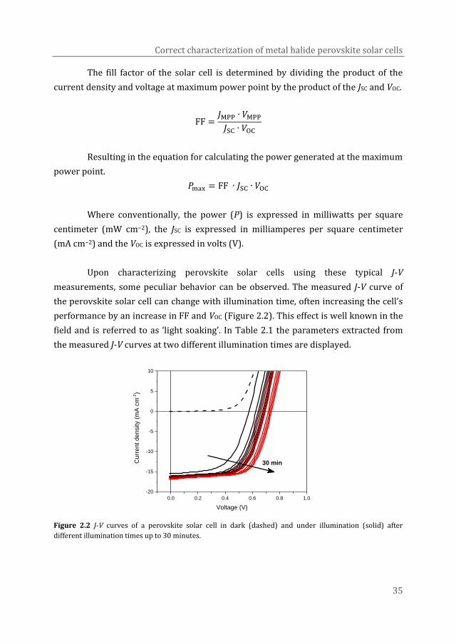
Correct characterization of metal halide perovskite solar cells
35
The fill factor of the solar cell is determined by dividing the product of the
current density and voltage at maximum power point by the product of the JSC and VOC.
FF =𝐽MPP ∙ 𝑉MPP
𝐽SC ∙ 𝑉OC
Resulting in the equation for calculating the power generated at the maximum
power point.
𝑃max = FF ∙ 𝐽SC ∙ 𝑉OC
Where conventionally, the power (P) is expressed in milliwatts per square
centimeter (mW cm−2), the JSC is expressed in milliamperes per square centimeter
(mA cm−2) and the VOC is expressed in volts (V).
Upon characterizing perovskite solar cells using these typical J-V
measurements, some peculiar behavior can be observed. The measured J-V curve of
the perovskite solar cell can change with illumination time, often increasing the cell’s
performance by an increase in FF and VOC (Figure 2.2). This effect is well known in the
field and is referred to as ‘light soaking’. In Table 2.1 the parameters extracted from
the measured J-V curves at two different illumination times are displayed.
0.0 0.2 0.4 0.6 0.8 1.0
-20
-15
-10
-5
0
5
10
Curr
ent density (
mA
cm
-2)
Voltage (V)
30 min
Figure 2.2 J-V curves of a perovskite solar cell in dark (dashed) and under illumination (solid) after
different illumination times up to 30 minutes.
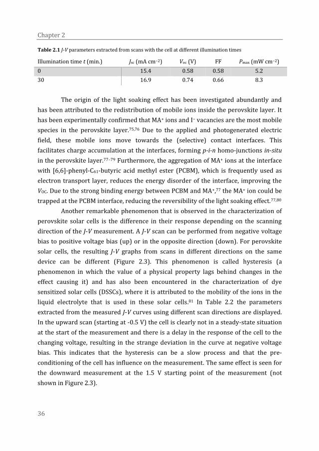
Chapter 2
36
Table 2.1 J-V parameters extracted from scans with the cell at different illumination times
Illumination time t (min.) Jsc (mA cm−2) Voc (V) FF Pmax (mW cm−2)
0 15.4 0.58 0.58 5.2
30 16.9 0.74 0.66 8.3
The origin of the light soaking effect has been investigated abundantly and
has been attributed to the redistribution of mobile ions inside the perovskite layer. It
has been experimentally confirmed that MA+ ions and I− vacancies are the most mobile
species in the perovskite layer.75,76 Due to the applied and photogenerated electric
field, these mobile ions move towards the (selective) contact interfaces. This
facilitates charge accumulation at the interfaces, forming p-i-n homo-junctions in-situ
in the perovskite layer.77–79 Furthermore, the aggregation of MA+ ions at the interface
with [6,6]-phenyl-C61-butyric acid methyl ester (PCBM), which is frequently used as
electron transport layer, reduces the energy disorder of the interface, improving the
VOC. Due to the strong binding energy between PCBM and MA+,77 the MA+ ion could be
trapped at the PCBM interface, reducing the reversibility of the light soaking effect.77,80
Another remarkable phenomenon that is observed in the characterization of
perovskite solar cells is the difference in their response depending on the scanning
direction of the J-V measurement. A J-V scan can be performed from negative voltage
bias to positive voltage bias (up) or in the opposite direction (down). For perovskite
solar cells, the resulting J-V graphs from scans in different directions on the same
device can be different (Figure 2.3). This phenomenon is called hysteresis (a
phenomenon in which the value of a physical property lags behind changes in the
effect causing it) and has also been encountered in the characterization of dye
sensitized solar cells (DSSCs), where it is attributed to the mobility of the ions in the
liquid electrolyte that is used in these solar cells.81 In Table 2.2 the parameters
extracted from the measured J-V curves using different scan directions are displayed.
In the upward scan (starting at -0.5 V) the cell is clearly not in a steady-state situation
at the start of the measurement and there is a delay in the response of the cell to the
changing voltage, resulting in the strange deviation in the curve at negative voltage
bias. This indicates that the hysteresis can be a slow process and that the pre-
conditioning of the cell has influence on the measurement. The same effect is seen for
the downward measurement at the 1.5 V starting point of the measurement (not
shown in Figure 2.3).
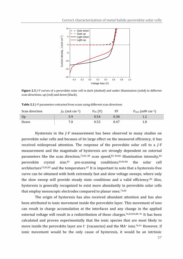
Correct characterization of metal halide perovskite solar cells
37
-0.4 -0.2 0.0 0.2 0.4 0.6 0.8 1.0
-20
-15
-10
-5
0
5
10
Curr
ent density, J (
mA
cm
-2)
Voltage bias (V)
Dark down
Dark up
Light down
Light up
Figure 2.3 J-V curves of a perovskite solar cell in dark (dashed) and under illumination (solid) in different
scan directions, up (red) and down (black).
Table 2.2 J-V parameters extracted from scans using different scan directions
Scan direction JSC (mA cm−2) VOC (V) FF Pmax (mW cm−2)
Up 5.9 0.54 0.38 1.2
Down 7.0 0.53 0.47 1.8
Hysteresis in the J-V measurement has been observed in many studies on
perovskite solar cells and because of its large effect on the measured efficiency, it has
received widespread attention. The response of the perovskite solar cell to a J-V
measurement and the magnitude of hysteresis are strongly dependent on external
parameters like the scan direction,73,82–85 scan speed,82–84,86 illumination intensity,86
perovskite crystal size,82 pre-scanning conditions,83,84,86 the solar cell
architecture73,83,85 and the temperature.87 It is important to note that a hysteresis-free
curve can be obtained with both extremely fast and slow voltage sweeps, where only
the slow sweep will provide steady state conditions and a valid efficiency.83 Also,
hysteresis is generally recognized to exist more abundantly in perovskite solar cells
that employ mesoscopic electrodes compared to planar ones.73,85
The origin of hysteresis has also received abundant attention and has also
been attributed to ionic movement inside the perovskite layer. This movement of ions
can result in charge accumulation at the interfaces and any change in the applied
external voltage will result in a redistribution of these charges.76,83,85,88–91 It has been
calculated and proven experimentally that the ionic species that are most likely to
move inside the perovskite layer are I− (vacancies) and the MA+ ions.76,91 However, if
ionic movement would be the only cause of hysteresis, it would be an intrinsic
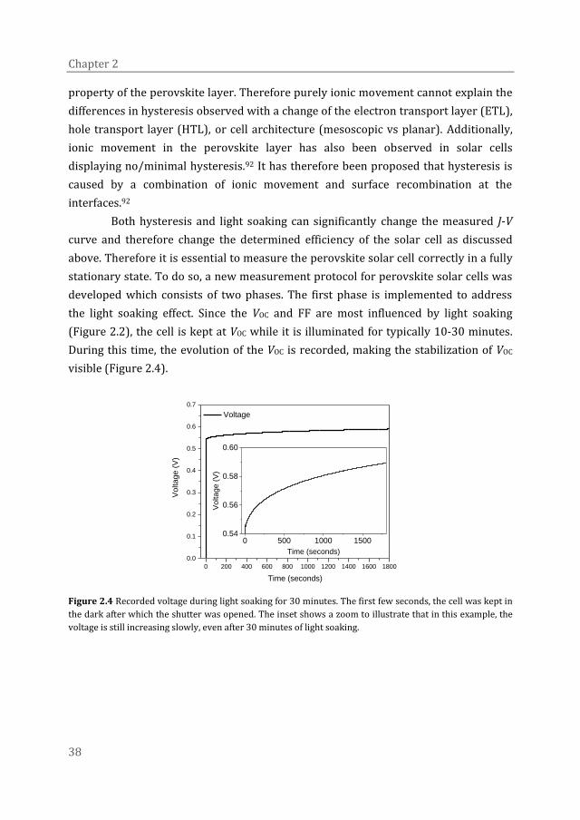
Chapter 2
38
property of the perovskite layer. Therefore purely ionic movement cannot explain the
differences in hysteresis observed with a change of the electron transport layer (ETL),
hole transport layer (HTL), or cell architecture (mesoscopic vs planar). Additionally,
ionic movement in the perovskite layer has also been observed in solar cells
displaying no/minimal hysteresis.92 It has therefore been proposed that hysteresis is
caused by a combination of ionic movement and surface recombination at the
interfaces.92
Both hysteresis and light soaking can significantly change the measured J-V
curve and therefore change the determined efficiency of the solar cell as discussed
above. Therefore it is essential to measure the perovskite solar cell correctly in a fully
stationary state. To do so, a new measurement protocol for perovskite solar cells was
developed which consists of two phases. The first phase is implemented to address
the light soaking effect. Since the VOC and FF are most influenced by light soaking
(Figure 2.2), the cell is kept at VOC while it is illuminated for typically 10-30 minutes.
During this time, the evolution of the VOC is recorded, making the stabilization of VOC
visible (Figure 2.4).
0 200 400 600 800 1000 1200 1400 1600 1800
0.0
0.1
0.2
0.3
0.4
0.5
0.6
0.7
Voltage (
V)
Time (seconds)
Voltage
0 500 1000 15000.54
0.56
0.58
0.60
Voltage (
V)
Time (seconds)
Figure 2.4 Recorded voltage during light soaking for 30 minutes. The first few seconds, the cell was kept in
the dark after which the shutter was opened. The inset shows a zoom to illustrate that in this example, the
voltage is still increasing slowly, even after 30 minutes of light soaking.
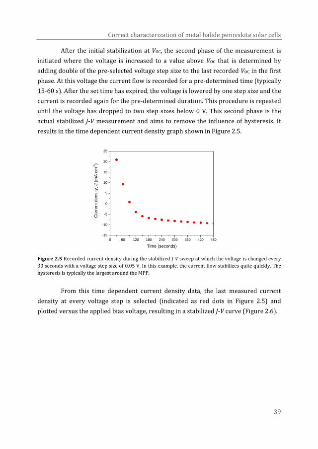
Correct characterization of metal halide perovskite solar cells
39
After the initial stabilization at VOC, the second phase of the measurement is
initiated where the voltage is increased to a value above VOC that is determined by
adding double of the pre-selected voltage step size to the last recorded VOC in the first
phase. At this voltage the current flow is recorded for a pre-determined time (typically
15-60 s). After the set time has expired, the voltage is lowered by one step size and the
current is recorded again for the pre-determined duration. This procedure is repeated
until the voltage has dropped to two step sizes below 0 V. This second phase is the
actual stabilized J-V measurement and aims to remove the influence of hysteresis. It
results in the time dependent current density graph shown in Figure 2.5.
0 60 120 180 240 300 360 420 480
-15
-10
-5
0
5
10
15
20
25
Curr
ent density,
J (
mA
cm
-2)
Time (seconds)
Figure 2.5 Recorded current density during the stabilized J-V sweep at which the voltage is changed every
30 seconds with a voltage step size of 0.05 V. In this example, the current flow stabilizes quite quickly. The
hysteresis is typically the largest around the MPP.
From this time dependent current density data, the last measured current
density at every voltage step is selected (indicated as red dots in Figure 2.5) and
plotted versus the applied bias voltage, resulting in a stabilized J-V curve (Figure 2.6).
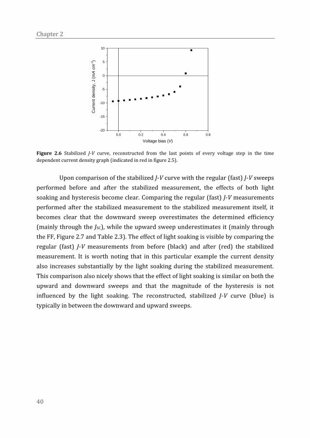
Chapter 2
40
0.0 0.2 0.4 0.6 0.8
-20
-15
-10
-5
0
5
10
Curr
ent density, J (
mA
cm
-2)
Voltage bias (V)
Figure 2.6 Stabilized J-V curve, reconstructed from the last points of every voltage step in the time
dependent current density graph (indicated in red in figure 2.5).
Upon comparison of the stabilized J-V curve with the regular (fast) J-V sweeps
performed before and after the stabilized measurement, the effects of both light
soaking and hysteresis become clear. Comparing the regular (fast) J-V measurements
performed after the stabilized measurement to the stabilized measurement itself, it
becomes clear that the downward sweep overestimates the determined efficiency
(mainly through the JSC), while the upward sweep underestimates it (mainly through
the FF, Figure 2.7 and Table 2.3). The effect of light soaking is visible by comparing the
regular (fast) J-V measurements from before (black) and after (red) the stabilized
measurement. It is worth noting that in this particular example the current density
also increases substantially by the light soaking during the stabilized measurement.
This comparison also nicely shows that the effect of light soaking is similar on both the
upward and downward sweeps and that the magnitude of the hysteresis is not
influenced by the light soaking. The reconstructed, stabilized J-V curve (blue) is
typically in between the downward and upward sweeps.

Correct characterization of metal halide perovskite solar cells
41
-0.5 0.0 0.5 1.0
-20
-15
-10
-5
0
5
10
Down before stabilized
Up before stabilized
Stabilized
Down after stabilized
Up after stabilized
Curr
ent density, J (
mA
cm
-2)
Voltage bias (V)
Figure 2.7 Reconstructed J-V curve from the stabilized sweep (blue), regular (fast) J-V sweeps recorded
before (black) and after (red) the stabilized J-V measurement in both up (dashed) and down (solid) scan
directions.
Table 2.3 J-V parameters extracted from the stabilized measurement and regular (fast) J-V sweeps in both
scan directions recorded before and after the stabilized measurement
JSC (mA cm−2) VOC (V) FF Pmax (mW cm−2)
Up before stabilized 5.9 0.54 0.38 1.2
Down before stabilized 7.0 0.53 0.47 1.8
Stabilized 9.2 0.59 0.56 3.0
Up after stabilized 8.8 0.59 0.41 2.1
Down after stabilized 10.9 0.59 0.53 3.4
Protocols in which the light soaking of the solar cell is performed at JSC instead
of VOC conditions have also been explored. The change in JSC is however usually not as
significant as that of the VOC and it was found that prolonged light exposure of the cell
under short circuit conditions can degrade a sub-optimal perovskite solar cell
significantly before the stabilized measurement has started. With the demonstrated
method, the light soaking time in the first phase and the voltage step size and the
stabilization time at every voltage step in the second phase can be selected as desired,
making the method suitable for any kind of perovskite solar cell, independent of the
time the cell requires to stabilize.
It must be noted that sub-optimal (low performance) perovskite solar cells in
general exhibit stronger light soaking and hysteresis effects compared to their high-
performing analogues. This could result in a high performance cell with small
hysteresis appearing to be less efficient than a low performance cell that exhibits large
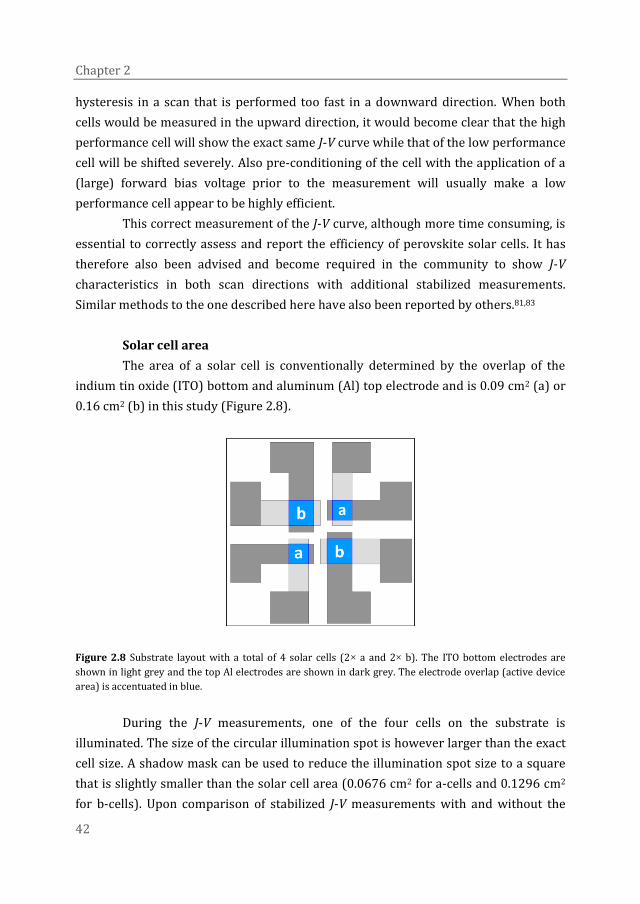
Chapter 2
42
hysteresis in a scan that is performed too fast in a downward direction. When both
cells would be measured in the upward direction, it would become clear that the high
performance cell will show the exact same J-V curve while that of the low performance
cell will be shifted severely. Also pre-conditioning of the cell with the application of a
(large) forward bias voltage prior to the measurement will usually make a low
performance cell appear to be highly efficient.
This correct measurement of the J-V curve, although more time consuming, is
essential to correctly assess and report the efficiency of perovskite solar cells. It has
therefore also been advised and become required in the community to show J-V
characteristics in both scan directions with additional stabilized measurements.
Similar methods to the one described here have also been reported by others.81,83
Solar cell area
The area of a solar cell is conventionally determined by the overlap of the
indium tin oxide (ITO) bottom and aluminum (Al) top electrode and is 0.09 cm2 (a) or
0.16 cm2 (b) in this study (Figure 2.8).
Figure 2.8 Substrate layout with a total of 4 solar cells (2× a and 2× b). The ITO bottom electrodes are
shown in light grey and the top Al electrodes are shown in dark grey. The electrode overlap (active device
area) is accentuated in blue.
During the J-V measurements, one of the four cells on the substrate is
illuminated. The size of the circular illumination spot is however larger than the exact
cell size. A shadow mask can be used to reduce the illumination spot size to a square
that is slightly smaller than the solar cell area (0.0676 cm2 for a-cells and 0.1296 cm2
for b-cells). Upon comparison of stabilized J-V measurements with and without the

Correct characterization of metal halide perovskite solar cells
43
use of a shadow mask, it is clear that the unmasked measurement givers a higher solar
cell efficiency (Figure 2.9).
-0.5 0.0 0.5 1.0
-20
-15
-10
-5
0
5
10
masked
unmaskedC
urr
ent density,
J (
mA
cm
-2)
Voltage bias (V)
Figure 2.9 Reconstructed J-V curves from stabilized J-V measurements performed without (red) and with
the use of a shadow mask (black).
Table 2.4 J-V parameters extracted from the stabilized measurement sweeps with and without the use of a
shadow mask.
JSC (mA cm−2) VOC (V) FF Pmax (mW cm−2)
Masked 15.5 0.63 0.69 6.7
No mask 16.5 0.65 0.66 7.1
This indicates that without the use of a shadow mask, the area from which
charges are being collected is larger than the electrode overlap, causing an
underestimation of the active area resulting in an overestimation of the efficiency. The
importance of using a shadow mask when performing J-V measurements has been
discussed in literature for DSSCs, where the origin of the overestimation of JSC is the
absorption of scattered- and diffuse light from outside the cell area.81,93–95 The
necessity of using a shadow mask to avoid overestimation of the JSC has also been
discussed in the field of organic photovoltaics (OPV), where the origin of the
introduced error is quite different. In OPV, the current generation is overestimated
mainly when a highly conductive grade of poly(3,4-ethylenedioxytiophene):
poly(styrenesulfonate) (PEDOT:PSS) is used. Due to its high conductivity the
PEDOT:PSS can transport charges that are generated outside the solar cell area to the
electrode where they can be extracted.94,96–100 In our perovskite solar cells, the
PEDOT:PSS that is used however, is not highly conductive. It has been reported though
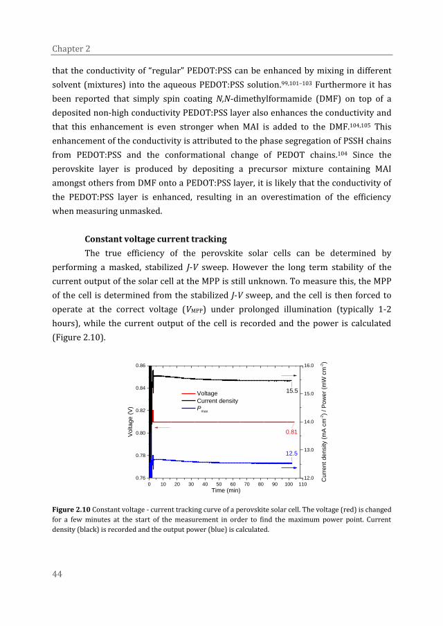
Chapter 2
44
that the conductivity of “regular” PEDOT:PSS can be enhanced by mixing in different
solvent (mixtures) into the aqueous PEDOT:PSS solution.99,101–103 Furthermore it has
been reported that simply spin coating N,N-dimethylformamide (DMF) on top of a
deposited non-high conductivity PEDOT:PSS layer also enhances the conductivity and
that this enhancement is even stronger when MAI is added to the DMF.104,105 This
enhancement of the conductivity is attributed to the phase segregation of PSSH chains
from PEDOT:PSS and the conformational change of PEDOT chains.104 Since the
perovskite layer is produced by depositing a precursor mixture containing MAI
amongst others from DMF onto a PEDOT:PSS layer, it is likely that the conductivity of
the PEDOT:PSS layer is enhanced, resulting in an overestimation of the efficiency
when measuring unmasked.
Constant voltage current tracking
The true efficiency of the perovskite solar cells can be determined by
performing a masked, stabilized J-V sweep. However the long term stability of the
current output of the solar cell at the MPP is still unknown. To measure this, the MPP
of the cell is determined from the stabilized J-V sweep, and the cell is then forced to
operate at the correct voltage (VMPP) under prolonged illumination (typically 1-2
hours), while the current output of the cell is recorded and the power is calculated
(Figure 2.10).
0 10 20 30 40 50 60 70 80 90 100 110
0.76
0.78
0.80
0.82
0.84
0.86
Voltage
Current density
Pmax
Time (min)
Vo
lta
ge
(V
)
0.81
12.0
13.0
14.0
15.0
16.0
Cu
rre
nt
de
nsity (
mA
cm
-2)
/ P
ow
er
(mW
cm
-2)
15.5
12.5
Figure 2.10 Constant voltage - current tracking curve of a perovskite solar cell. The voltage (red) is changed
for a few minutes at the start of the measurement in order to find the maximum power point. Current
density (black) is recorded and the output power (blue) is calculated.

Correct characterization of metal halide perovskite solar cells
45
In Figure 2.10, the cell shows a nice stabilization over time, however cells that
stabilize even faster as well as cells that do not reach a stable current output within 2
hours have also been observed. Also in this measurement, there is a strong relation
between the overall performance of the solar cell and the stability at the MPP where
sub-optimal cells have low stability and good cells exhibit excellent stability.
2.3 Wavelength dependent spectral responsivity
To determine a truly meaningful solar cell efficiency, it should be related to
the solar spectrum that is incident on the earth’s surface. Upon passing through the
earth’s atmosphere, the spectrum that is emitted by the sun (extraterrestrial spectrum
in Figure 2.11) is significantly modified due to light absorption of compounds that are
present in the atmosphere (mainly ozone (O3), oxygen (O2), carbon dioxide (CO2) and
water (H2O)). Since the spectrum changes when traveling through the atmosphere, the
distance the light travels through it is also of importance. This distance is dependent
on the position on the globe since the angle at which the light travels through the
atmosphere changes as illustrated in the inset of Figure 2.11. Therefore the
convention is to report the distance the light has traveled through the atmosphere in
units of “air mass” (AM), where AM 1.0 is once the thickness of the atmosphere and
AM 1.5 is 1.5 times this distance. The letters D and G are often added to this notation
to indicate the direct (D) or global (G) spectra, where the global spectrum also takes
scattered light into account. In order to make reported solar cell efficiencies
comparable, the spectrum that is conventionally used for solar cell measurements is
the AM 1.5G spectrum with an overall illumination intensity of 100 mW cm−2 and the
solar cell at a temperature of 25 °C. The spectrum of the light source used in J-V
measurements (in our experiments a tungsten-halogen lamp with added filters)
resembles the AM 1.5G spectrum quite well but does not match it exactly. Therefore
there will always be a small discrepancy in the efficiency determined in the J-V setup
and the efficiency determined using the accepted standard illumination spectrum.
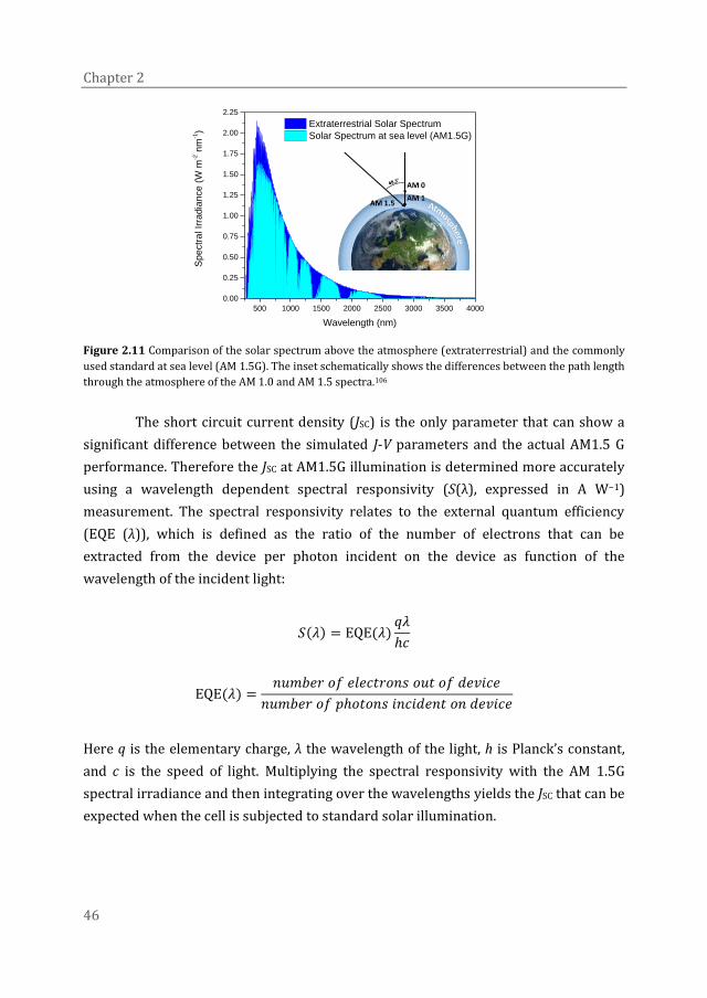
Chapter 2
46
500 1000 1500 2000 2500 3000 3500 4000
0.00
0.25
0.50
0.75
1.00
1.25
1.50
1.75
2.00
2.25
Sp
ectr
al Ir
rad
iance
(W
m-2 n
m-1)
Wavelength (nm)
Extraterrestrial Solar Spectrum
Solar Spectrum at sea level (AM1.5G)
Figure 2.11 Comparison of the solar spectrum above the atmosphere (extraterrestrial) and the commonly
used standard at sea level (AM 1.5G). The inset schematically shows the differences between the path length
through the atmosphere of the AM 1.0 and AM 1.5 spectra.106
The short circuit current density (JSC) is the only parameter that can show a
significant difference between the simulated J-V parameters and the actual AM1.5 G
performance. Therefore the JSC at AM1.5G illumination is determined more accurately
using a wavelength dependent spectral responsivity (S(λ), expressed in A W−1)
measurement. The spectral responsivity relates to the external quantum efficiency
(EQE (λ)), which is defined as the ratio of the number of electrons that can be
extracted from the device per photon incident on the device as function of the
wavelength of the incident light:
𝑆(𝜆) = EQE(𝜆)𝑞𝜆
ℎ𝑐
EQE(𝜆) =𝑛𝑢𝑚𝑏𝑒𝑟 𝑜𝑓 𝑒𝑙𝑒𝑐𝑡𝑟𝑜𝑛𝑠 𝑜𝑢𝑡 𝑜𝑓 𝑑𝑒𝑣𝑖𝑐𝑒
𝑛𝑢𝑚𝑏𝑒𝑟 𝑜𝑓 𝑝ℎ𝑜𝑡𝑜𝑛𝑠 𝑖𝑛𝑐𝑖𝑑𝑒𝑛𝑡 𝑜𝑛 𝑑𝑒𝑣𝑖𝑐𝑒
Here q is the elementary charge, λ the wavelength of the light, h is Planck’s constant,
and c is the speed of light. Multiplying the spectral responsivity with the AM 1.5G
spectral irradiance and then integrating over the wavelengths yields the JSC that can be
expected when the cell is subjected to standard solar illumination.

Correct characterization of metal halide perovskite solar cells
47
The correct power conversion efficiency (PCE) can then be calculated using:
PCE =𝑃max
𝑃in
=𝐹𝐹 ∙ 𝑉OC ∙ 𝐽SC
𝑃in
=𝐹𝐹 ∙ 𝑉OC
𝑃in
∫ 𝑆(𝜆) ∙ 𝐸𝐴𝑀 1.5𝐺(𝜆) d𝜆
Where Pin is the power of the incident light and EAM 1.5G(λ) is spectral irradiance
(expressed in W m−2 nm−1) of the AM 1.5G spectrum. In addition to the JSC under
AM 1.5G illumination of the solar cell, the EQE shows the spectral regions that
contribute to photocurrent generation.
The EQE measurement is performed using low intensity modulated
monochromatic light in combination with lock-in amplification to determine the
response per wavelength. This low light intensity measurement however does not
necessarily represent the EQE values of the solar cell at an illumination intensity of
approximately 100 mW cm−2. Therefore the EQE is also measured with the use of an
additional bias illumination. The bias light intensity is set so that it generates a charge
carrier density in the device that is comparable to that of the device under AM 1.5G (1
sun) illumination conditions. An ideal solar cell would exhibit a linear response of
current density to the light intensity. For sub-optimal perovskite solar cells however,
this response is often sublinear and the EQE at high light intensity is (much) lower
than that at low light intensity (Figure 2.12).
300 400 500 600 700 8000.0
0.2
0.4
0.6
0.8
1.0
18.5 mA cm-2
15.8 mA cm-2
EQ
E
Wavelength (nm) Figure 2.12 EQE at low (black squares) and high (green circles) light intensity of a perovskite solar cell that
exhibits a sublinear response of current density to the light intensity. The integrated short circuit current
density (JSC) is displayed in black and green for the low and high light intensity respectively.

Chapter 2
48
2.4 Light intensity dependent measurements
Besides J-V and EQE measurements that provide the PCE of the measured
solar cell, light intensity dependent measurements of the JSC and VOC can give us insight
in the recombination mechanisms that are limiting the device performance.
The VOC of a solar cell equals the difference between quasi-Fermi levels for
electrons and holes and can be written as:107
𝑉OC =𝐸g
𝑞−
𝑘𝑇
𝑞𝑙𝑛 [
𝑁V𝑁C
𝑛𝑝]
In this equation Eg is the bandgap, k is Boltzmann's constant, T is the temperature, Nv
and Nc are the density of states in the valence and conduction bands, and n and p are
the electron and hole densities. At open circuit all charges must recombine and hence
the charge generation rate (G) must equal the recombination rate (R), R = G.
When bimolecular (Langevin) recombination prevails (R ≈ RBR) this implies
that:108,109
𝑅BR = 𝑘BR𝑛𝑝 = 𝐺
Here kBR is the bimolecular recombination constant. Because G is proportional to the
light intensity I0 (G = gI0) it follows that:
𝑉OC =𝐸g
𝑞−
𝑘𝑇
𝑞𝑙𝑛 [
𝑘BR𝑁V𝑁C
𝑔𝐼0
]
For dominant trap-assisted recombination the recombination rate (R ≈ RSRH)
can be expressed by the Shockley−Read−Hall (SRH) equation:108,109
𝑅SRH =𝐶n𝐶p𝑁t
𝐶n(𝑛 + 𝑛1) + 𝐶p(𝑝 + 𝑝1)𝑛𝑝 = 𝐺
In this equation Nt is the trap density, and Cn and Cp are the trap coefficients for
electron and holes respectively that denote the probability per unit time that the
electron (hole) in the conduction (valence) band will be captured when the trap is
filled with a hole (electron). n1 and p1 are the thermally occupied trap densities.
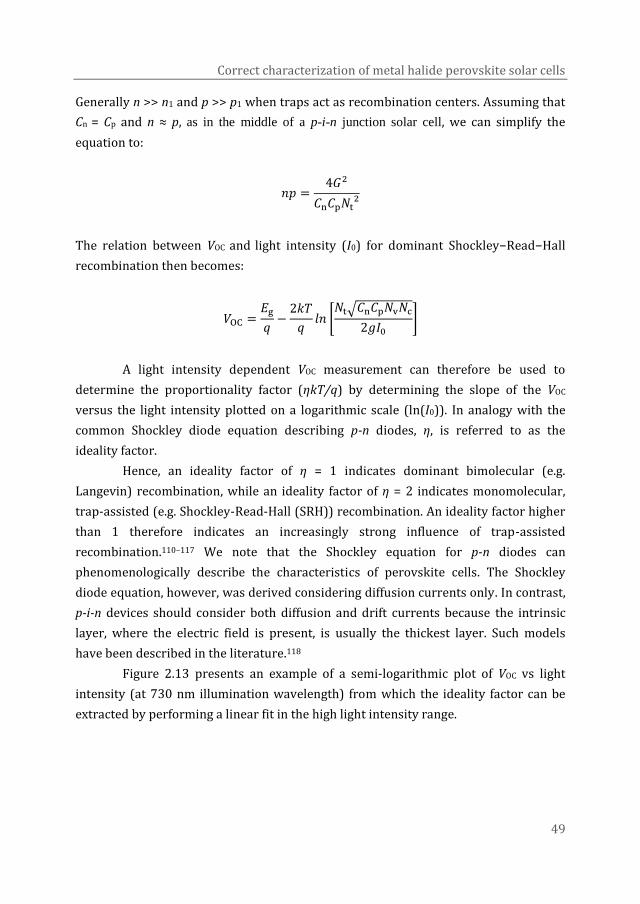
Correct characterization of metal halide perovskite solar cells
49
Generally n >> n1 and p >> p1 when traps act as recombination centers. Assuming that
Cn = Cp and n ≈ p, as in the middle of a p-i-n junction solar cell, we can simplify the
equation to:
𝑛𝑝 =4𝐺2
𝐶n𝐶p𝑁t2
The relation between VOC and light intensity (I0) for dominant Shockley−Read−Hall
recombination then becomes:
𝑉OC =𝐸g
𝑞−
2𝑘𝑇
𝑞𝑙𝑛 [
𝑁t√𝐶n𝐶p𝑁v𝑁c
2𝑔𝐼0
]
A light intensity dependent VOC measurement can therefore be used to
determine the proportionality factor (ηkT/q) by determining the slope of the VOC
versus the light intensity plotted on a logarithmic scale (ln(I0)). In analogy with the
common Shockley diode equation describing p-n diodes, η, is referred to as the
ideality factor.
Hence, an ideality factor of η = 1 indicates dominant bimolecular (e.g.
Langevin) recombination, while an ideality factor of η = 2 indicates monomolecular,
trap-assisted (e.g. Shockley-Read-Hall (SRH)) recombination. An ideality factor higher
than 1 therefore indicates an increasingly strong influence of trap-assisted
recombination.110–117 We note that the Shockley equation for p-n diodes can
phenomenologically describe the characteristics of perovskite cells. The Shockley
diode equation, however, was derived considering diffusion currents only. In contrast,
p-i-n devices should consider both diffusion and drift currents because the intrinsic
layer, where the electric field is present, is usually the thickest layer. Such models
have been described in the literature.118
Figure 2.13 presents an example of a semi-logarithmic plot of VOC vs light
intensity (at 730 nm illumination wavelength) from which the ideality factor can be
extracted by performing a linear fit in the high light intensity range.
Chapter 2
50
0.1 1 10 100 10000.2
0.4
0.6
0.8
1.0
Op
en
-circu
it v
olta
ge
(V
)
Photon flux / 1015
(cm-2
s-1)
Figure 2.13 Example of light intensity dependent VOC plotted in a logarithmic (ln) scale (red squares). A
black line with a slope of 25.9 meV (= kT/q at 300 K) has been added to indicate the slope of a device with
an ideality factor of 1.
From this curve it is clear that at high light intensities, the slope is about 25.9
meV (= kT/q), meaning that the ideality factor is (close to) 1 and band-to-band
recombination is dominant. However, the slope is much steeper, even η > 2, for low
light intensities, indicating dominant trap-assisted recombination. By performing this
measurement on one device using different illumination areas, we see that the slope at
low light intensity depends on the illuminated area and is lower when a larger part of
the solar cell is illuminated (Figure 2.14).
0.1 1 10 100 10000.2
0.4
0.6
0.8
1.0
Open-c
ircuit v
oltage (
V)
Photon flux / 1015
(cm-2 s
-1)
illuminated area (cm2)
0.0314
0.0676
0.1296
>0.1600 (no mask)
~1 sun
for perovskite
Figure 2.14 Light intensity dependent VOC of a perovskite solar cell using 730 nm illumination wavelength
with different illumination areas. The solar cell area (electrode overlap) is 0.16 cm2, a charge carrier density
similar to that of the perovskite solar cell under 1 sun AM1.5G illumination is indicated with the orange
dashed line. The black line represents the slope for η = 1.
Correct characterization of metal halide perovskite solar cells
51
The higher ideality factor at low light intensities in Figure 2.14 is an artefact
caused by the leakage current as a result of a low shunt resistance. Since the physical
device area (0.16 cm2) of the device remains the same, so do the number of leakage
paths. When the illuminated area is increased, the number of charges generated
increases proportionally, while the leakage current and voltage loss remain constant
in first approximation. Hence, by illuminating the entire cell area the effect of these
shunt paths at a lower photon flux are minimized, causing band-to-band
recombination to become dominant and the ideality factor to become (close to) 1 at a
lower absolute photon flux.
For an ideal solar cell, a linear dependence of the short-circuit current (ISC) on
the illumination intensity (I0) is expected. The resulting graph can be fitted using a
power law dependence, (𝐼SC ∝ 𝐼0𝛼) where the α is 1 for an ideal device and an α of
0.75 has been observed for devices that have a highly unbalanced electron and hole
mobility.119–121 In Figure 2.15, examples of the light intensity dependent ISC and EQE
measurements using different illumination wavelengths are shown.
1 10 100
1
10
100
1000
~1 sun
for perovskite
530 nm = 0.98
730 nm = 0.97
Short
-circuit c
urr
ent (
A)
Photon flux / 1015
(cm-2 s
-1)
1 10 1000.0
0.2
0.4
0.6
0.8
1.0
Photon flux / 1015
(cm-2 s
-1)
EQ
E
EQE 530nm bias illumination
EQE 730nm bias illumination
~1 sun
for perovskite
Figure 2.15 Example of light intensity dependent Isc (left) and EQE (right) of a perovskite solar cell using
530 nm (green squares) and 730 nm (red squares) light illumination wavelength. In the left figure, the
exponent α value obtained from a power-law fit is displayed and in both figures, a charge carrier density
similar to that of the perovskite solar cell under 1 sun AM1.5G illumination is indicated with the orange
dashed line.
Chapter 2
52
2.5 Scanning electron microscopy of perovskite
layers
Scanning electron microscopy (SEM) is a valuable technique in assessing the
morphology of the produced perovskite layers by taking top-view or cross-section
images of the deposited layer. However, as with the electrical characterization of
perovskite layers, making correct SEM images of perovskite layers requires some
additional attention. The most common way to prepare samples for SEM analysis of
perovskite layers is to deposit them on top of a glass slide, either with or without the
selective contact layer (e.g. PEDOT:PSS) in between the perovskite and the glass.
Deposition of a perovskite layer on top of the selective contact will give a better
representation of the perovskite layer that is used in a solar cell since the properties
of the layer on which the perovskite layer is deposited influence the nucleation and
crystal growth of the perovskite layer. The nucleation and crystal growth of the
perovskite structure is however even more sensitive than that. It was found that even
the layer underneath the selective contact influences the crystallization behavior
(Figure 2.16).
Figure 2.16 SEM image of a 400 nm thick perovskite layer deposited on top of a patterned glass/ITO
substrate with a 50 nm PEDOT:PSS layer between the glass/ITO and perovskite layer at 1.000x
magnification with a scale bar of 10 µm.
The perovskite layer formed on top of ITO/PEDOT:PSS possesses less
pinholes and is much more compact than that formed on top of Glass/PEDOT:PSS. In
order to assess the quality and crystallinity of the perovskite layer in a solar cell, it is
Correct characterization of metal halide perovskite solar cells
53
therefore vital that the SEM measurement is performed on a section that has an ITO
bottom layer. The origin of this strong difference in crystallization of the perovskite
structure is still unknown. One obvious cause could be a difference in nucleation and
crystal growth due to differences in roughness of the PEDOT:PSS layer on top of ITO
or on top of glass. AFM measurements however confirm that the roughness of the
PEDOT:PSS is not much different on top of ITO or glass (Figure 2.17) Additionally,
grounding the perovskite layer is important to avoid charging of the layer.
Figure 2.17 AFM height images of the surface of clean glass (a) and ITO (d) and glass and ITO with a
PEDOT:PSS layer on top (b and c respectively). Calculated root mean squared (Rq) and arithmetical mean
deviation (Ra) surface roughness values are displayed beneath the images. All image sizes are 5 μm × 5 μm
and the height bar spans from 0 (dark red) to (a) 10, (b) 8, (c) 12, and (d) 30 nm (light pink).
2.6 References
1 A. Kojima, K. Teshima, Y. Shirai, and T. Miyasaka, J. Am. Chem. Soc., 2009, 131, 6050–
6051.
2 H.-S Kim, C.-R. Lee, J.-H. Im, K.-B. Lee, T. Moehl, A. Marchioro, S.-J. Moon, R. Humphry-
baker, J.-H. Yum, J. E. Moser, M. Grätzel and N.-G. Park, Sci. Rep., 2012, 2, 591.
3 M. M. Lee, J. Teuscher, T. Miyasaka, T. N. Murakami and H. J. Snaith, Science, 2012, 338,
643–647.
4 W. S. Yang, B.-W. Park, E. H. Jung, N. J. Jeon, Y. C. Kim, D. U. Lee, S. S. Shin, J. Seo, E. K. Kim,
J. H. Noh and S. I. Seok, Science, 2017, 356, 1376–1379.
5 D. Bi, W. Tress, M. I. Dar, P. Gao, J. Luo, C. Renevier, K. Schenk, A. Abate, F. Giordano, J.-P.
Correa Baena, J.-D. Decoppet, S. M. Zakeeruddin, M. K. Nazeeruddin, M. Grätzel and A.
Hagfeldt, Sci. Adv., 2016, 2, 1501170.
6 M. Saliba, T. Matsui, J.-Y. Seo, K. Domanski, J.-P. Correa-Baena, M. K. Nazeeruddin, S. M.
Zakeeruddin, W. Tress, A. Abate, A. Hagfeldt and M. Grätzel, Energy Environ. Sci., 2016, 9,
1989–1997.
7 M. a. Green, A. Ho-Baillie and H. J. Snaith, Nat. Photonics, 2014, 8, 506–514.
8 Y. Zhao and K. Zhu, J. Phys. Chem. Lett., 2014, 5, 4175–4186.
a b c d
Rq = 1.73 nm Ra = 1.17 nm Rq = 1.32 nm Ra = 1.03 nm Rq = 2.12 nm Ra = 1.71 nm Rq = 5.64 nm Ra = 4.61 nm
Chapter 2
54
9 J. Burschka, N. Pellet, S.-J. Moon, R. Humphry-Baker, P. Gao, M. K. Nazeeruddin and M.
Grätzel, Nature, 2013, 499, 316–319.
10 N.-G. Park, J. Phys. Chem. Lett., 2013, 4, 2423–2429.
11 S. Lv, S. Pang, Y. Zhou, N. P. Padture, H. Hu, L. Wang, X. Zhou, H. Zhu, L. Zhang, C. Huang
and G. Cui, Phys. Chem. Chem. Phys., 2014, 16, 19206–19211.
12 J.-W. Lee, D.-J. Seol, A.-N. Cho and N.-G. Park, Adv. Mater., 2014, 26, 4991–4998.
13 G. E. Eperon, S. D. Stranks, C. Menelaou, M. B. Johnston, L. M. Herz and H. J. Snaith, Energy
Environ. Sci., 2014, 7, 982-988.
14 Y. Zhou, M. Yang, S. Pang, K. Zhu and N. P. Padture, J. Am. Chem. Soc., 2016, 138, 5535–
5538.
15 F. C. Hanusch, E. Wiesenmayer, E. Mankel, A. Binek, P. Angloher, C. Fraunhofer, N.
Giesbrecht, J. M. Feckl, W. Jaegermann, D. Johrendt, T. Bein and P. Docampo, J. Phys.
Chem. Lett., 2014, 5, 2791–2795.
16 M. Kulbak, D. Cahen and G. Hodes, J. Phys. Chem. Lett., 2015, 6, 2452–2456.
17 F. Giustino and H. J. Snaith, ACS Energy Lett., 2016, 1, 1233–1240.
18 S. Yang, W. Fu, Z. Zhang, H. Chen and C.-Z. Li, J. Mater. Chem. A, 2017, 5, 11462–11482.
19 S. F. Hoefler, G. Trimmel and T. Rath, Monatshefte für Chemie - Chem. Mon., 2017, 148,
795–826.
20 P. V. Kamat, J. Bisquert and J. Buriak, ACS Energy Lett., 2017, 2, 904–905.
21 K. Wang, Z. Liang, X. Wang and X. Cui, Adv. Electron. Mater., 2015, 1, 1500089.
22 H. Yu, F. Wang, F. Xie, W. Li, J. Chen and N. Zhao, Adv. Funct. Mater., 2014, 24, 7102–7108.
23 Q. Chen, H. Zhou, Y. Fang, A. Z. Stieg, T.-B. Song, H.-H. Wang, X. Xu, Y. Liu, S. Lu, J. You, P.
Sun, J. McKay, M. S. Goorsky and Y. Yang, Nat. Commun., 2015, 6, 7269.
24 Y. Tian, M. Peter, E. Unger, M. Abdellah, K. Zheng, T. Pullerits, A. Yartsev, V. Sundström
and I. G. Scheblykin, Phys. Chem. Chem. Phys., 2015, 17, 24978–24987.
25 S. Colella, E. Mosconi, P. Fedeli, A. Listorti, F. Gazza, F. Orlandi, P. Ferro, T. Besagni, A.
Rizzo, G. Calestani, G. Gigli, F. De Angelis and R. Mosca, Chem. Mater., 2013, 25, 4613–
4618.
26 J. H. Heo, M. H. Lee, M. H. Jang and S. H. Im, J. Mater. Chem. A, 2016, 4, 17636–17642.
27 M. M. Tavakoli, L. Gu, Y. Gao, C. Reckmeier, J. He, A. L. Rogach, Y. Yao and Z. Fan, Sci. Rep.,
2015, 5, 14083.
28 S. Colella, E. Mosconi, G. Pellegrino, A. Alberti, V. L. P. Guerra, S. Masi, A. Listorti, A. Rizzo,
G. G. Condorelli, F. De Angelis and G. Gigli, J. Phys. Chem. Lett., 2014, 5, 3532–3538.
29 Y. Tidhar, E. Edri, H. Weissman, D. Zohar, D. Cahen, B. Rybtchinski and S. Kirmayer, J. Am.
Chem. Soc., 2014, 136, 13249–13256.
30 H. Yu, H. Lu, F. Xie, S. Zhou and N. Zhao, Adv. Funct. Mater., 2016, 26, 1411–1419.
31 M. Yang, Y. Zhou, Y. Zeng, C.-S. Jiang, N. P. Padture and K. Zhu, Adv. Mater., 2015, 27,
6363–6370.
32 H.-B. Kim, H. Choi, J. Jeong, S. Kim, B. Walker, S. Song and J. Y. Kim, Nanoscale, 2014, 6,
6679.

Correct characterization of metal halide perovskite solar cells
55
33 C. Roldán-Carmona, P. Gratia, I. Zimmermann, G. Grancini, P. Gao, M. Graetzel and M. K.
Nazeeruddin, Energy Environ. Sci., 2015, 8, 3550–3556.
34 N. K. Noel, S. N. Habisreutinger, B. Wenger, M. T. Klug, M. T. Hörantner, M. B. Johnston, R.
J. Nicholas, D. T. Moore and H. J. Snaith, Energy Environ. Sci., 2017, 10, 145.
35 P.-W. Liang, C.-Y. Liao, C.-C. Chueh, F. Zuo, S. T. Williams, X.-K. Xin, J. Lin and A. K.-Y. Jen,
Adv. Mater., 2014, 26, 3748–3754.
36 Y. C. Kim, N. J. Jeon, J. H. Noh, W. S. Yang, J. Seo, J. S. Yun, A. Ho-Baillie, S. Huang, M. A.
Green, J. Seidel, T. K. Ahn and S. I. Seok, Adv. Energy Mater., 2016, 6, 1502104.
37 Z. Xiao, C. Bi, Y. Shao, Q. Dong, Q. Wang, Y. Yuan, C. Wang, Y. Gao and J. Huang, Energy
Environ. Sci., 2014, 7, 2619–2623.
38 Y. Wu, A. Islam, X. Yang, C. Qin, J. Liu, K. Zhang, W. Peng and L. Han, Energy Environ. Sci.,
2014, 7, 2934–2938.
39 P. Mao, Q. Zhou, Z. Jin, H. Li and J. Wang, ACS Appl. Mater. Interfaces, 2016, 8, 23837–
23843.
40 J.-H. Im, H.-S. Kim and N.-G. Park, APL Mater., 2014, 2, 081510.
41 C.-H. Chiang, Z.-L. Tseng and C.-G. Wu, J. Mater. Chem. A, 2014, 2, 15897–15903.
42 Y. Zhao and K. Zhu, J. Mater. Chem. A, 2015, 3, 9086–9091.
43 A. Wakamiya, M. Endo, T. Sasamori, N. Tokitoh, Y. Ogomi, S. Hayase and Y. Murata, Chem.
Lett., 2014, 43, 711–713.
44 P. Luo, Z. Liu, W. Xia, C. Yuan, J. Cheng and Y. Lu, ACS Appl. Mater. Interfaces, 2015, 7,
2708–2714.
45 Q. Chen, H. Zhou, Z. Hong, S. Luo, H.-S. Duan, H.-H. Wang, Y. Liu, G. Li and Y. Yang, J. Am.
Chem. Soc., 2014, 136, 622–625.
46 M. R. Leyden, L. K. Ono, S. R. Raga, Y. Kato, S. Wang and Y. Qi, J. Mater. Chem. A, 2014, 2,
18742–18745.
47 L. K. Ono, M. R. Leyden, S. Wang and Y. Qi, J. Mater. Chem. A, 2016, 4, 6693–6713.
48 M. R. Leyden, M. V. Lee, S. R. Raga and Y. Qi, J. Mater. Chem. A, 2015, 3, 16097–16103.
49 F. Hao, C. C. Stoumpos, Z. Liu, R. P. H. Chang and M. G. Kanatzidis, J. Am. Chem. Soc., 2014,
136, 16411–16419.
50 T. Zhang, N. Guo, G. Li, X. Qian, L. Li and Y. Zhao, J. Mater. Chem. A, 2016, 4, 3245–3248.
51 P. Luo, Z. Liu, W. Xia, C. Yuan, J. Cheng, C. Xu and Y. Lu, J. Mater. Chem. A, 2015, 3, 22949–
22959.
52 J. Xiong, B. Yang, R. Wu, C. Cao, Y. Huang, C. Liu, Z. Hu, H. Huang, Y. Gao and J. Yang, Org.
Electron., 2015, 24, 106–112.
53 N. J. Jeon, J. H. Noh, Y. C. Kim, W. S. Yang, S. Ryu and S. I. Seok, Nat. Mater., 2014, 13, 897–
903.
54 H. D. Kim, H. Ohkita, H. Benten and S. Ito, Adv. Mater., 2016, 28, 917–922.
55 N. Ahn, D.-Y. Son, I.-H. Jang, S. M. Kang, M. Choi and N.-G. Park, J. Am. Chem. Soc., 2015,
137, 8696–8699.
56 M. Liu, M. B. Johnston and H. J. Snaith, Nature, 2013, 501, 395–398.

Chapter 2
56
57 C. Wehrenfennig, M. Liu, H. J. Snaith, M. B. Johnston and L. M. Herz, Energy Environ. Sci.,
2014, 7, 2269.
58 W. Ke, D. Zhao, C. R. Grice, A. J. Cimaroli, G. Fang and Y. Yan, J. Mater. Chem. A, 2015, 3,
23888–23894.
59 W. Qiu, T. Merckx, M. Jaysankar, C. Masse de la Huerta, L. Rakocevic, W. Zhang, U. W.
Paetzold, R. Gehlhaar, L. Froyen, J. Poortmans, D. Cheyns, H. J. Snaith and P. Heremans,
Energy Environ. Sci., 2016, 9, 484–489.
60 W. Zhang, M. Saliba, D. T. Moore, S. K. Pathak, M. T. Hörantner, T. Stergiopoulos, S. D.
Stranks, G. E. Eperon, J. A. Alexander-Webber, A. Abate, A. Sadhanala, S. Yao, Y. Chen, R.
H. Friend, L. A. Estroff, U. Wiesner and H. J. Snaith, Nat. Commun., 2015, 6, 6142.
61 M. Salado, L. Contreras-Bernal, L. Caliò, A. Todinova, C. López-Santos, S. Ahmad, A.
Borras, J. Idígoras and J. A. Anta, J. Mater. Chem. A, 2017, 5, 10917–10927.
62 F. Li and M. Liu, J. Mater. Chem. A, 2017, 5, 15447–15459.
63 G. E. Eperon, S. N. Habisreutinger, T. Leijtens, B. J. Bruijnaers, J. J. Van Franeker, D. W.
Dequilettes, S. Pathak, R. J. Sutton, G. Grancini, D. S. Ginger, R. A. J. Janssen, A. Petrozza
and H. J. Snaith, ACS Nano, 2015, 9, 9380–9393.
64 J. J. van Franeker, K. H. Hendriks, B. J. Bruijnaers, M. W. G. M. Verhoeven, M. M. Wienk and
R. A. J. Janssen, Adv. Energy Mater., 2017, 7, 1601822.
65 A. Dualeh, N. Tétreault, T. Moehl, P. Gao, M. K. Nazeeruddin and M. Grätzel, Adv. Funct.
Mater., 2014, 24, 3250–3258.
66 V. L. Pool, B. Dou, D. G. Van Campen, T. R. Klein-Stockert, F. S. Barnes, S. E. Shaheen, M. I.
Ahmad, M. F. A. M. van Hest and M. F. Toney, Nat. Commun., 2017, 8, 14075.
67 C. Bi, Y. Shao, Y. Yuan, Z. Xiao, C. Wang, Y. Gao and J. Huang, J. Mater. Chem. A, 2014, 2,
18508–18514.
68 S. R. Raga, M.-C. Jung, M. V. Lee, M. R. Leyden, Y. Kato and Y. Qi, Chem. Mater., 2015, 27,
1597–1603.
69 M. Saliba, K. W. Tan, H. Sai, D. T. Moore, T. Scott, W. Zhang, L. A. Estroff, U. Wiesner and H.
J. Snaith, J. Phys. Chem. C, 2014, 118, 17171–17177.
70 R. Kang, J.-E. Kim, J.-S. Yeo, S. Lee, Y.-J. Jeon and D.-Y. Kim, J. Phys. Chem. C, 2014, 118,
26513–26520.
71 M.-F. Xu, H. Zhang, S. Zhang, H. L. Zhu, H.-M. Su, J. Liu, K. S. Wong, L.-S. Liao and W. C. H.
Choy, J. Mater. Chem. A, 2015, 3, 14424–14430.
72 L. Huang, Z. Hu, J. Xu, K. Zhang, J. Zhang and Y. Zhu, Sol. Energy Mater. Sol. Cells, 2015,
141, 377–382.
73 E. Zimmermann, K. K. Wong, M. Müller, H. Hu, P. Ehrenreich, M. Kohlstädt, U. Würfel, S.
Mastroianni, G. Mathiazhagan, A. Hinsch, T. P. Gujar, M. Thelakkat, T. Pfadler and L.
Schmidt-Mende, APL Mater., 2016, 4, 091901.
74 L. K. Ono, E. J. Juárez-Pérez and Y. Qi, ACS Appl. Mater. Interfaces, 2017, 9, 30197-30246.
75 Y. Yuan, Q. Wang, Y. Shao, H. Lu, T. Li, A. Gruverman and J. Huang, Adv. Energy Mater.,
2016, 6, 1501803.
Correct characterization of metal halide perovskite solar cells
57
76 Y. Yuan and J. Huang, Acc. Chem. Res., 2016, 49, 286–293.
77 T. Zhang, S. H. Cheung, X. Meng, L. Zhu, Y. Bai, C. H. Y. Ho, S. Xiao, Q. Xue, S. K. So and S.
Yang, J. Phys. Chem. Lett., 2017, 8, 5069-5076.
78 Y. Deng, Z. Xiao and J. Huang, Adv. Energy Mater., 2015, 5, 1500721.
79 C. Zhao, B. Chen, X. Qiao, L. Luan, K. Lu and B. Hu, Adv. Energy Mater., 2015, 5, 1500279.
80 S. Shao, M. Abdu-Aguye, L. Qiu, L.-H. Lai, J. Liu, S. Adjokatse, F. Jahani, M. E. Kamminga, G.
H. ten Brink, T. T. M. Palstra, B. J. Kooi, J. C. Hummelen and M. A. Loi, Energy Environ. Sci.,
2016, 9, 2444–2452.
81 X. Yang, M. Yanagida and L. Han, Energy Environ. Sci., 2013, 6, 54–66.
82 H.-S. Kim and N.-G. Park, J. Phys. Chem. Lett., 2014, 5, 2927-2934.
83 E. L. Unger, E. T. Hoke, C. D. Bailie, W. H. Nguyen, A. R. Bowring, T. Heumüller, M. G.
Christoforo and M. D. McGehee, Energy Environ. Sci., 2014, 7, 3690–3698.
84 J. A. Christians, J. S. Manser and P. V. Kamat, J. Phys. Chem. Lett., 2015, 6, 852–857.
85 H. J. Snaith, A. Abate, J. M. Ball, G. E. Eperon, T. Leijtens, N. K. Noel, S. D. Stranks, J. T.-W.
Wang, K. Wojciechowski and W. Zhang, J. Phys. Chem. Lett., 2014, 5, 1511–1515.
86 W. Tress, N. Marinova, T. Moehl, S. M. Zakeeruddin, M. K. Nazeeruddin and M. Grätzel,
Energy Environ. Sci., 2015, 8, 995–1004.
87 L. K. Ono, S. R. Raga, S. Wang, Y. Kato and Y. Qi, J. Mater. Chem. A, 2015, 3, 9074–9080.
88 J.-P. Correa-Baena, A. Abate, M. Saliba, W. Tress, T. Jesper Jacobsson, M. Grätzel and A.
Hagfeldt, Energy Environ. Sci., 2017, 10, 710–727.
89 W. Tress, J. P. Correa Baena, M. Saliba, A. Abate and M. Graetzel, Adv. Energy Mater., 2016,
6, 1600396.
90 C. Li, S. Tscheuschner, F. Paulus, P. E. Hopkinson, J. Kießling, A. Köhler, Y. Vaynzof and S.
Huettner, Adv. Mater., 2016, 28, 2446–2454.
91 D. A. Egger, A. M. Rappe and L. Kronik, Acc. Chem. Res., 2016, 49, 573–581.
92 P. Calado, A. M. Telford, D. Bryant, X. Li, J. Nelson, B. C. O’Regan and P. R. F. Barnes, Nat.
Commun., 2016, 7, 13831.
93 S. Ito, M. K. Nazeeruddin, P. Liska, P. Comte, R. Charvet, P. Péchy, M. Jirousek, A. Kay, S. M.
Zakeeruddin and M. Grätzel, Prog. Photovolt. Res. Appl., 2006, 14, 589–601.
94 H. J. Snaith, Energy Environ. Sci., 2012, 5, 6513-6520.
95 I. Chung, B. Lee, J. He, R. P. H. Chang and M. G. Kanatzidis, Nature, 2012, 485, 486–489.
96 E. Zimmermann, P. Ehrenreich, T. Pfadler, J. A. Dorman, J. Weickert and L. Schmidt-
Mende, Nat. Photonics, 2014, 8, 669–672.
97 A. Cravino, P. Schilinsky and C. J. Brabec, Adv. Funct. Mater., 2007, 17, 3906–3910.
98 S. A. Gevorgyan, J. E. Carlé, R. Søndergaard, T. T. Larsen-Olsen, M. Jørgensen and F. C.
Krebs, Sol. Energy Mater. Sol. Cells, 2013, 110, 24–35.
99 W. J. Potscavage Jr., Adv. Mater., 2013, 25, 4825.
100 H. J. Snaith, Nat. Photonics, 2012, 6, 337–340.
101 O. Bubnova, Z. U. Khan, H. Wang, S. Braun, D. R. Evans, M. Fabretto, P. Hojati-Talemi, D.
Dagnelund, J.-B. Arlin, Y. H. Geerts, S. Desbief, D. W. Breiby, J. W. Andreasen, R. Lazzaroni,
Chapter 2
58
W. M. Chen, I. Zozoulenko, M. Fahlman, P. J. Murphy, M. Berggren and X. Crispin, Nat.
Mater., 2013, 13, 190–194.
102 A. M. Nardes, R. A. J. Janssen and M. Kemerink, Adv. Funct. Mater., 2008, 18, 865–871.
103 S. K. M. Jönsson, J. Birgerson, X. Crispin, G. Greczynski, W. Osikowicz, A. W. Denier van
der Gon, W. R. Salaneck and M. Fahlman, Synth. Met., 2003, 139, 1–10.
104 Y. Xia, K. Sun, J. Chang and J. Ouyang, J. Mater. Chem. A, 2015, 3, 15897–15904.
105 Z. Yu, Y. Xia, D. Du and J. Ouyang, ACS Appl. Mater. Interfaces, 2016, 8, 11629–11638.
106 Solar Spectral Irradiance: ASTM G-173,
http://rredc.nrel.gov/solar/spectra/am1.5/ASTMG173/ASTMG173.html, (accessed 3
November 2017).
107 W. Shockley and H. J. H. Queisser, J. Appl. Phys., 1961, 32, 510–519.
108 T. S. Sherkar, C. Momblona, L. Gil-Escrig, J. Ávila, M. Sessolo, H. J. Bolink and L. J. A.
Koster, ACS Energy Lett., 2017, 2, 1214–1222.
109 T. Kirchartz, B. E. Pieters, J. Kirkpatrick, U. Rau and J. Nelson, Phys. Rev. B, 2011, 83,
115209.
110 G.-J. A. H. Wetzelaer, M. Scheepers, A. M. Sempere, C. Momblona, J. Ávila and H. J. Bolink,
Adv. Mater., 2015, 27, 1837–1841.
111 N. K. Elumalai and A. Uddin, Energy Environ. Sci., 2016, 9, 391–410.
112 R. N. Hall, The Institution of Electrical Engineers, 1960, 3047 E, 923-931.
113 T. Kirchartz, F. Deledalle, P. S. Tuladhar, J. R. Durrant and J. Nelson, J. Phys. Chem. Lett.,
2013, 4, 2371–2376.
114 K. Tvingstedt, L. Gil-Escrig, C. Momblona, P. Rieder, D. Kiermasch, M. Sessolo, A.
Baumann, H. J. Bolink and V. Dyakonov, ACS Energy Lett., 2017, 2, 424–430.
115 W. Shockley and W. T. Read, Phys. Rev., 1952, 87, 835–842.
116 N. Marinova, W. Tress, R. Humphry-Baker, M. I. Dar, V. Bojinov, S. M. Zakeeruddin, M. K.
Nazeeruddin and M. Grätzel, ACS Nano, 2015, 9, 4200–4209.
117 M. M. Mandoc, F. B. Kooistra, J. C. Hummelen, B. De Boer and P. W. M. Blom, Appl. Phys.
Lett., 2007, 91, 263505.
118 K. Taretto, U. Rau and J. H. Werner, Appl. Phys. A Mater. Sci. Process., 2003, 77, 865–871.
119 S. R. Cowan, A. Roy and A. J. Heeger, Phys. Rev. B, 2010, 82, 245207.
120 L. J. A. Koster, V. D. Mihailetchi, H. Xie and P. W. M. Blom, Appl. Phys. Lett., 2005, 87,
203502.
121 P. Schilinsky, C. Waldauf and C. J. Brabec, Appl. Phys. Lett., 2002, 81, 3885–3887.


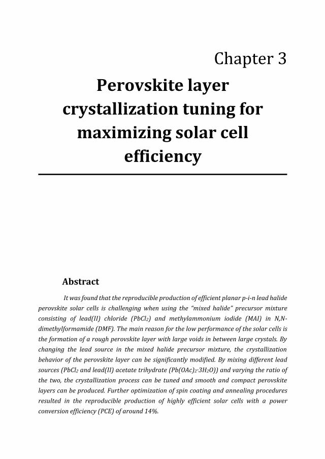
Chapter 3
Perovskite layer
crystallization tuning for
maximizing solar cell
efficiency
Abstract
It was found that the reproducible production of efficient planar p-i-n lead halide
perovskite solar cells is challenging when using the “mixed halide” precursor mixture
consisting of lead(II) chloride (PbCl2) and methylammonium iodide (MAI) in N,N-
dimethylformamide (DMF). The main reason for the low performance of the solar cells is
the formation of a rough perovskite layer with large voids in between large crystals. By
changing the lead source in the mixed halide precursor mixture, the crystallization
behavior of the perovskite layer can be significantly modified. By mixing different lead
sources (PbCl2 and lead(II) acetate trihydrate (Pb(OAc)2·3H2O)) and varying the ratio of
the two, the crystallization process can be tuned and smooth and compact perovskite
layers can be produced. Further optimization of spin coating and annealing procedures
resulted in the reproducible production of highly efficient solar cells with a power
conversion efficiency (PCE) of around 14%.

Chapter 3
62
3.1 Introduction
The intense research on lead halide perovskite solar cells in recent years has
resulted in highly efficient devices as well as an improved understanding of the
opportunities for using this material in solar cells. Apart from the attractive physical
properties like a high absorption coefficient,1,2 almost ideal bandgap, high charge
mobilities,3,4 and low exciton binding energy,5 the most important property of the
perovskite material is the tolerance towards composition and processing methods it
displays. By changing the composition of the perovskite material, changes can be made
to the physical properties like bandgap6 and higher stability.7 This allows optimization
of the material for specific applications (e.g. multi-junction solar cells). More
importantly from a processing point of view however, a specific composition of
perovskite (e.g. CH3NH3PbI3) can be produced from different precursor and solvent
combinations.8–12 In such case, a change in the precursor composition and solvent can
be used to tune the crystallization behavior.13–16 This has resulted in the application of
a large variety of precursor compositions and deposition techniques that can yield high
quality perovskite films.
In the early years of solid state perovskite solar cell research, the two most used
perovskite formulations were the ‘tri-iodide’ and ‘mixed halide’ precursor mixtures.
Where the ‘tri-iodide’ consists of methylammonium iodide (MAI) and lead(II) iodide
(PbI2) in a 1 : 1 molar ratio and the ‘mixed halide’ precursor mixture consists of MAI
and lead(II) chloride (PbCl2) in a 3 : 1 molar ratio to provide the 3 equivalents of iodide
required for the formation of the perovskite structure (MAPbI3).17–27
The main differences between these two recipes are the higher charge mobility
and larger diffusion length28 and the overall superior photovoltaic performance of
perovskite layers obtained from the mixed halide precursor. Where the initial thought
was that the chloride ions intercalate into the perovskite structure (hence the ‘mixed
halide’ name),18,19,21,25,27 it was later shown that only trace amounts of chloride could be
found in the perovskite layer in completed devices.29–31 Therefore the currently
accepted conclusion is that even with the use of the mixed halide precursor solution the
regular MAPbI3 perovskite is formed, and that the increased photovoltaic performance
is caused by improvement of the perovskite layer quality.29,30,32 Here, the mixed halide
perovskite recipe is used as a starting point for optimization of the perovskite solar cell
efficiency. The steps in the optimization procedure are shown and discussed in this
chapter.
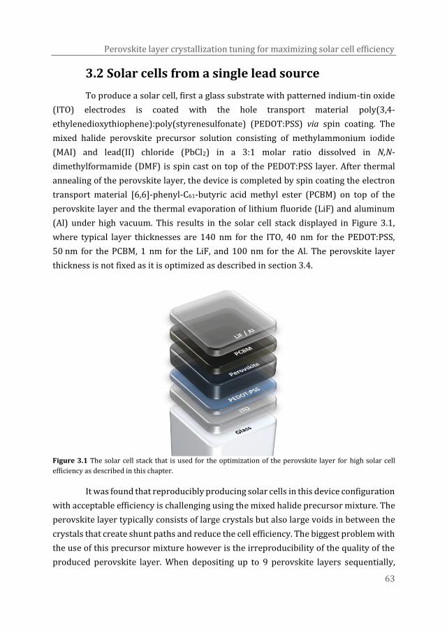
Perovskite layer crystallization tuning for maximizing solar cell efficiency
63
3.2 Solar cells from a single lead source
To produce a solar cell, first a glass substrate with patterned indium-tin oxide
(ITO) electrodes is coated with the hole transport material poly(3,4-
ethylenedioxythiophene):poly(styrenesulfonate) (PEDOT:PSS) via spin coating. The
mixed halide perovskite precursor solution consisting of methylammonium iodide
(MAI) and lead(II) chloride (PbCl2) in a 3:1 molar ratio dissolved in N,N-
dimethylformamide (DMF) is spin cast on top of the PEDOT:PSS layer. After thermal
annealing of the perovskite layer, the device is completed by spin coating the electron
transport material [6,6]-phenyl-C61-butyric acid methyl ester (PCBM) on top of the
perovskite layer and the thermal evaporation of lithium fluoride (LiF) and aluminum
(Al) under high vacuum. This results in the solar cell stack displayed in Figure 3.1,
where typical layer thicknesses are 140 nm for the ITO, 40 nm for the PEDOT:PSS,
50 nm for the PCBM, 1 nm for the LiF, and 100 nm for the Al. The perovskite layer
thickness is not fixed as it is optimized as described in section 3.4.
Figure 3.1 The solar cell stack that is used for the optimization of the perovskite layer for high solar cell
efficiency as described in this chapter.
It was found that reproducibly producing solar cells in this device configuration
with acceptable efficiency is challenging using the mixed halide precursor mixture. The
perovskite layer typically consists of large crystals but also large voids in between the
crystals that create shunt paths and reduce the cell efficiency. The biggest problem with
the use of this precursor mixture however is the irreproducibility of the quality of the
produced perovskite layer. When depositing up to 9 perovskite layers sequentially,
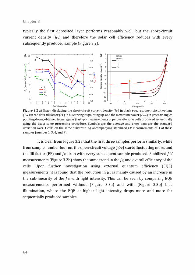
Chapter 3
64
typically the first deposited layer performs reasonably well, but the short-circuit
current density (JSC) and therefore the solar cell efficiency reduces with every
subsequently produced sample (Figure 3.2).
0 1 2 3 4 5 6 7 8 9 10
2
4
6
8
10
12
14a
JSC
VOC
FF
Pmax
Sample number
JS
C (
mA
cm
-2)
/ P
max (
mW
cm
-2)
0.3
0.4
0.5
0.6
0.7
0.8
0.9
1.0
VO
C (
V)
/ F
F
0.0 0.2 0.4 0.6 0.8
-14
-12
-10
-8
-6
-4
-2
0
2
4
6
8b
Curr
en
t de
nsity (
mA
cm
-2)
Voltage (V)
sample
number
1
3
4
9
Figure 3.2 a) Graph displaying the short-circuit current density (JSC) in black squares, open-circuit voltage
(VOC) in red dots, fill factor (FF) in blue triangles pointing up, and the maximum power (Pmax) in green triangles
pointing down, obtained from regular (fast) J-V measurements of perovskite solar cells produced sequentially
using the exact same processing procedure. Symbols are the average and error bars are the standard
deviation over 4 cells on the same substrate. b) Accompanying stabilized J-V measurements of 4 of these
samples (number 1, 3, 4, and 9).
It is clear from Figure 3.2a that the first three samples perform similarly, while
from sample number four on, the open-circuit voltage (VOC) starts fluctuating more, and
the fill factor (FF) and JSC drop with every subsequent sample produced. Stabilized J-V
measurements (Figure 3.2b) show the same trend in the JSC and overall efficiency of the
cells. Upon further investigation using external quantum efficiency (EQE)
measurements, it is found that the reduction in JSC is mainly caused by an increase in
the sub-linearity of the JSC with light intensity. This can be seen by comparing EQE
measurements performed without (Figure 3.3a) and with (Figure 3.3b) bias
illumination, where the EQE at higher light intensity drops more and more for
sequentially produced samples.

Perovskite layer crystallization tuning for maximizing solar cell efficiency
65
300 400 500 600 700 800 9000.0
0.1
0.2
0.3
0.4
0.5
0.6
0.7
0.8
0.9
1.0
sample number
1 (17.5 mA cm-2)
3 (17.5 mA cm-2)
4 (16.9 mA cm-2)
9 (15.6 mA cm-2)
EQ
E
Wavelength (nm)
a
300 400 500 600 700 800 900
0.0
0.1
0.2
0.3
0.4
0.5
0.6
0.7
0.8
0.9
1.0sample number
1 (12.9 mA cm-2)
3 (12.2 mA cm-2)
4 (11.1 mA cm-2)
9 ( 7.1 mA cm-2)
EQ
E
Wavelength (nm)
b
Figure 3.3 External quantum efficiency (EQE) plots of perovskite solar cells produced sequentially measured
under low- (a) and high- (b) illumination intensity.
All steps in the processing procedure were investigated and altered extensively
aiming to reduce this decrease of performance. The spin coating speed, duration, and
atmosphere of the perovskite layer were changed, the annealing time and temperature
was changed including complex and lengthy ramp annealing schemes, the hole
transport layer (HTL) and electron transport layer (ETL) were changed with several
alternatives, the atmosphere in which the layers are stored between spin coating and
annealing was changed, and even the precursor solution was changed, all without any
improvement in the reproducibility. Although the optimized production procedure
produces solar cells with an efficiency up to 8%, the irreproducibility of the perovskite
layer quality using this recipe is detrimental for the systematic investigation and
improvement of this new type of solar cell. Another approach is therefore required for
further increase of solar cell efficiency and systematic investigation of the perovskite
material for use in solar cell application.
3.3 Tuning of the crystallization speed using
multiple lead sources
As illustrated in section 3.2, the desired high efficiency (>10% PCE) solar cells
could not be produced using the mixed halide precursor mixture. During initial
experiments employing different lead sources in the mixed halide precursor solution, it
was noted that a precursor solution containing MAI and PbCl2 in DMF crystallizes
extremely slowly and only during annealing (visible by the color change from yellow to
dark brown), and eventually forms a rough perovskite layer. A precursor solution
containing MAI and lead(II) acetate trihydrate (Pb(OAc)2·3H2O) on the other hand,
crystallizes extremely fast, already turning light brown during spin coating. This is most
Chapter 3
66
likely caused by a more rapid formation and/or evaporation of the decomposition
products, contributing to faster crystal growth.8 Upon annealing of the formed film, the
light brown color changes to darker brown and an extremely smooth layer is formed
(root mean squared roughness (Rq) of 5 to 10 nm for ~400 nm thick perovskite layers
produced from MAI and Pb(OAc)2 versus Rq of ~120 nm for 275 nm thick perovskite
layers produced from MAI and PbCl2). The disadvantage of replacing all PbCl2 in the
precursor mixture with Pb(OAc)2·3H2O is that during annealing, the layer formed from
MAI and Pb(OAc)2·3H2O starts to form large cracks.
Upon closer analysis of the formed perovskite layers using scanning electron
microscopy (SEM), the crystallites formed from a precursor solution containing MAI
and PbCl2 are very large and are accompanied by large voids in between them (Figure
3.4, PbCl2 fraction = 1). The crystallites formed from a precursor solution containing
MAI and Pb(OAc)2·3H2O are extremely small but do form a completely closed layer in
between the large cracks that were observed visually (Figure 3.4, Pb(OAc)2·3H2O
fraction = 1). Since the crystallization behavior is so strongly influenced by the lead
source that is used in the precursor solution, both lead sources were used together in
different ratios in the precursor solution in order to tune the crystallization speed and
size of the crystallites, aiming to produce a compact perovskite layer with large crystals
to avoid the creation of shunt paths and maximize the charge transport efficiency.
During production of these perovskite layers, it was observed that the crystallization
speed can actually be controlled very well by changing the ratio of the two lead sources
in the precursor solution. Throughout the full range of ratios a higher fraction of
Pb(OAc)2·3H2O leads to faster perovskite formation and smoother perovskite layer
after annealing. SEM images of perovskite layers produced from precursor solutions
with different ratios of PbCl2 and Pb(OAc)2·3H2O are shown in Figure 3.4.
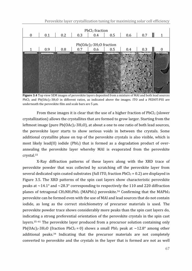
Perovskite layer crystallization tuning for maximizing solar cell efficiency
67
PbCl2 fraction 0 0.1 0.2 0.3 0.4 0.5 0.6 0.7 1
Pb(OAc)2·3H2O fraction
1 0.9 0.8 0.7 0.6 0.5 0.4 0.3 0
Figure 3.4 Top view SEM images of perovskite layers deposited from a mixture of MAI and both lead sources
PbCl2 and Pb(OAc)2·3H2O in different ratios, as indicated above the images. ITO and a PEDOT:PSS are
underneath the perovskite film and scale bars are 5 µm.
From these images it is clear that the use of a higher fraction of PbCl2 (slower
crystallization) allows the crystallites that are formed to grow larger. Starting from the
leftmost image (pure Pb(OAc)2·3H2O), at about a one to one ratio of both lead sources,
the perovskite layer starts to show serious voids in between the crystals. Some
additional crystallite phase on top of the perovskite crystals is also visible, which is
most likely lead(II) iodide (PbI2) that is formed as a degradation product of over-
annealing the perovskite layer whereby MAI is evaporated from the perovskite
crystal.33
X-Ray diffraction patterns of these layers along with the XRD trace of
perovskite powder that was collected by scratching off the perovskite layer from
several dedicated spin coated substrates (full ITO, fraction PbCl2 = 0.2) are displayed in
Figure 3.5. The XRD patterns of the spin cast layers show characteristic perovskite
peaks at ~14.1° and ~28.3° corresponding to respectively the 110 and 220 diffraction
planes of tetragonal CH3NH3PbI3 (MAPbI3) perovskite.34 Confirming that the MAPbI3
perovskite can be formed even with the use of MAI and lead sources that do not contain
iodide, as long as the correct stoichiometry of precursor materials is used. The
perovskite powder trace shows considerably more peaks than the spin cast layers do,
indicating a strong preferential orientation of the perovskite crystals in the spin cast
layers.35–41 The perovskite layer produced from a precursor solution containing only
Pb(OAc)2·3H2O (fraction PbCl2 = 0) shows a small PbI2 peak at ~12.8° among other
additional peaks.34 Indicating that the precursor materials are not completely
converted to perovskite and the crystals in the layer that is formed are not as well
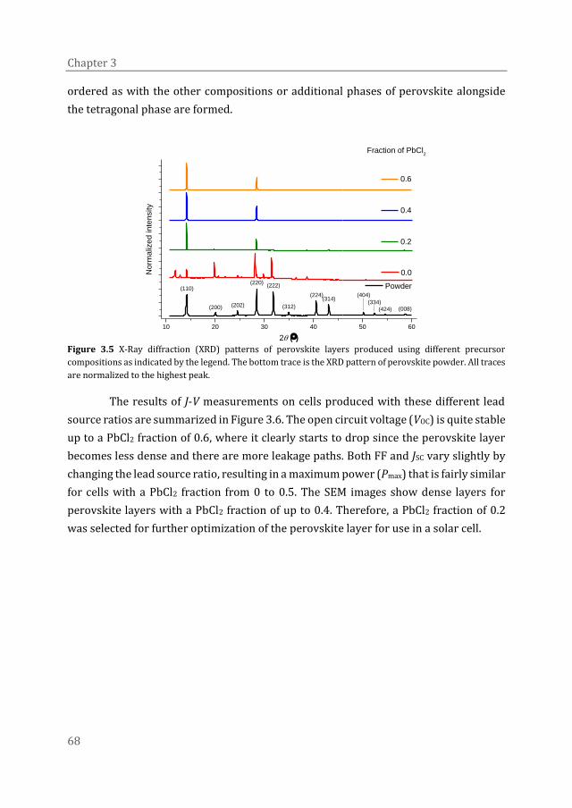
Chapter 3
68
ordered as with the other compositions or additional phases of perovskite alongside
the tetragonal phase are formed.
10 20 30 40 50 60
Fraction of PbCl2
No
rma
lize
d in
ten
sity
2 ()
0.6
0.4
0.2
0.0
Powder(110)
(200) (202)
(220)(222)
(312)
(224)(314)
(404)
(334)
(424) (008)
Figure 3.5 X-Ray diffraction (XRD) patterns of perovskite layers produced using different precursor
compositions as indicated by the legend. The bottom trace is the XRD pattern of perovskite powder. All traces
are normalized to the highest peak.
The results of J-V measurements on cells produced with these different lead
source ratios are summarized in Figure 3.6. The open circuit voltage (VOC) is quite stable
up to a PbCl2 fraction of 0.6, where it clearly starts to drop since the perovskite layer
becomes less dense and there are more leakage paths. Both FF and JSC vary slightly by
changing the lead source ratio, resulting in a maximum power (Pmax) that is fairly similar
for cells with a PbCl2 fraction from 0 to 0.5. The SEM images show dense layers for
perovskite layers with a PbCl2 fraction of up to 0.4. Therefore, a PbCl2 fraction of 0.2
was selected for further optimization of the perovskite layer for use in a solar cell.

Perovskite layer crystallization tuning for maximizing solar cell efficiency
69
0.0 0.2 0.4 0.6 0.8 1.0
2
4
6
8
10 J
SC
VOC
FF
Pmax
Fraction of PbCl2 in precursor solution
JS
C (
mA
cm
-2)
/ P
ma
x (
mW
cm
-2)
1.0 0.8 0.6 0.4 0.2 0.0
0.4
0.6
0.8
Fraction of Pb(OAc)2·3H
2O in precursor solution
VO
C (
V)
/ F
F
Figure 3.6 Graph displaying the short circuit current density (JSC) in black squares, open circuit voltage (VOC)
in red dots, fill factor (FF) in blue triangles pointing up, and maximum power (Pmax) in green triangles pointing
down, obtained from regular (fast) J-V measurements, of perovskite solar cells produced using precursor
mixtures containing different ratios of lead sources PbCl2 and Pb(OAc)2·3H2O. Symbols are the average and
error bars are the standard deviation over 4 cells on the same substrate.
3.4 Perovskite phase control
Additional crystallites (most likely PbI2) were observed on top of the
perovskite crystals in the SEM images shown in Figure 3.4. As mentioned in section 3.3,
the PbI2 crystals are probably formed as a degradation product by evaporating MAI
from the perovskite crystals, leaving PbI2 behind. Therefore, the effect of annealing
temperature and duration on the appearance and performance of the perovskite layer
was investigated. Figure 3.7 shows SEM images of the perovskite layers produced from
a precursor solution with a PbCl2 fraction of 0.2 that was annealed at different
temperatures with different durations. From these SEM images it is clear that the
additional crystallites only appear at annealing temperatures of >90 °C when annealing
for 10 minutes. When annealing for 30 minutes at 90 °C, the additional crystallites
appear to also starting forming, indicating that although the annealing temperature has
the strongest influence and should be kept below 110 °C to avoid PbI2 formation, also
the annealing time should be kept below 30 minutes.
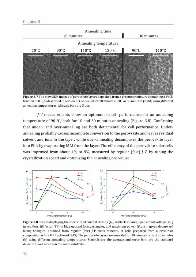
Chapter 3
70
Annealing time 10 minutes 30 minutes
Annealing temperature
70°C 90°C 110°C 130°C 90°C 110°C
Figure 3.7 Top view SEM images of perovskite layers deposited from a precursor mixture containing a PbCl2
fraction of 0.2, as described in section 3.3, annealed for 10 minutes (left) or 30 minutes (right) using different
annealing temperatures. All scale bars are 3 µm.
J-V measurements show an optimum in cell performance for an annealing
temperature of 90 °C, both for 10 and 30 minutes annealing (Figure 3.8). Confirming
that under- and over-annealing are both detrimental for cell performance. Under-
annealing probably causes incomplete conversion to the perovskite and leaves residual
solvent and ions in the layer, while over-annealing decomposes the perovskite layer
into PbI2 by evaporating MAI from the layer. The efficiency of the perovskite solar cells
was improved from about 4% to 8%, measured by regular (fast) J-V, by tuning the
crystallization speed and optimizing the annealing procedure.
70 90 110 130
0
2
4
6
8
10
12 JSC
VOC
FF
Pmax
Annealing temperature (°C)
JS
C (
mA
cm
-2)
/ P
ma
x (
mW
cm
-2)
a
0.5
0.7
0.9
1.1
VO
C (
V)
/ F
F
70 90 110
0
2
4
6
8
10
12 JSC
VOC
FF
Pmax
Annealing temperature (°C)
JS
C (
mA
cm
-2)
/ P
ma
x (
mW
cm
-2)
0.5
0.7
0.9
1.1
VO
C (
V)
/ F
F
b
Figure 3.8 Graphs displaying the short circuit current density (JSC) in black squares, open circuit voltage (VOC)
in red dots, fill factor (FF) in blue upward facing triangles, and maximum power (Pmax) in green downward
facing triangles, obtained from regular (fast) J-V measurements, of cells prepared from a precursor
composition with a 0.2 fraction of PbCl2. The perovskite layers are annealed for 10 minutes (a) and 30 minutes
(b) using different annealing temperatures. Symbols are the average and error bars are the standard
deviation over 4 cells on the same substrate.
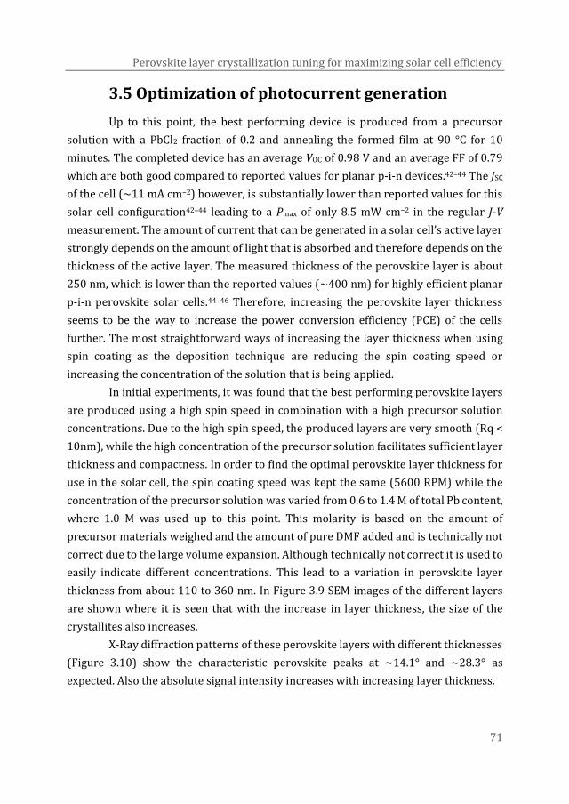
Perovskite layer crystallization tuning for maximizing solar cell efficiency
71
3.5 Optimization of photocurrent generation
Up to this point, the best performing device is produced from a precursor
solution with a PbCl2 fraction of 0.2 and annealing the formed film at 90 °C for 10
minutes. The completed device has an average VOC of 0.98 V and an average FF of 0.79
which are both good compared to reported values for planar p-i-n devices.42–44 The JSC
of the cell (~11 mA cm−2) however, is substantially lower than reported values for this
solar cell configuration42–44 leading to a Pmax of only 8.5 mW cm−2 in the regular J-V
measurement. The amount of current that can be generated in a solar cell’s active layer
strongly depends on the amount of light that is absorbed and therefore depends on the
thickness of the active layer. The measured thickness of the perovskite layer is about
250 nm, which is lower than the reported values (~400 nm) for highly efficient planar
p-i-n perovskite solar cells.44–46 Therefore, increasing the perovskite layer thickness
seems to be the way to increase the power conversion efficiency (PCE) of the cells
further. The most straightforward ways of increasing the layer thickness when using
spin coating as the deposition technique are reducing the spin coating speed or
increasing the concentration of the solution that is being applied.
In initial experiments, it was found that the best performing perovskite layers
are produced using a high spin speed in combination with a high precursor solution
concentrations. Due to the high spin speed, the produced layers are very smooth (Rq <
10nm), while the high concentration of the precursor solution facilitates sufficient layer
thickness and compactness. In order to find the optimal perovskite layer thickness for
use in the solar cell, the spin coating speed was kept the same (5600 RPM) while the
concentration of the precursor solution was varied from 0.6 to 1.4 M of total Pb content,
where 1.0 M was used up to this point. This molarity is based on the amount of
precursor materials weighed and the amount of pure DMF added and is technically not
correct due to the large volume expansion. Although technically not correct it is used to
easily indicate different concentrations. This lead to a variation in perovskite layer
thickness from about 110 to 360 nm. In Figure 3.9 SEM images of the different layers
are shown where it is seen that with the increase in layer thickness, the size of the
crystallites also increases.
X-Ray diffraction patterns of these perovskite layers with different thicknesses
(Figure 3.10) show the characteristic perovskite peaks at ~14.1° and ~28.3° as
expected. Also the absolute signal intensity increases with increasing layer thickness.
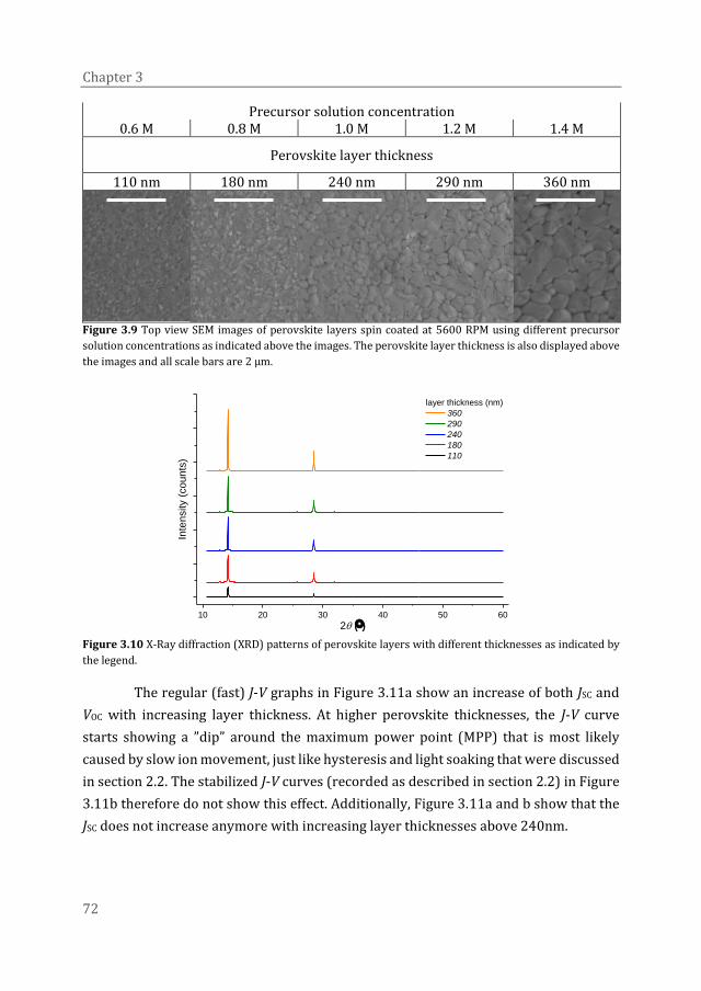
Chapter 3
72
Precursor solution concentration 0.6 M 0.8 M 1.0 M 1.2 M 1.4 M
Perovskite layer thickness
110 nm 180 nm 240 nm 290 nm 360 nm
Figure 3.9 Top view SEM images of perovskite layers spin coated at 5600 RPM using different precursor
solution concentrations as indicated above the images. The perovskite layer thickness is also displayed above
the images and all scale bars are 2 µm.
10 20 30 40 50 60
Inte
nsity (
co
un
ts)
2 ()
layer thickness (nm)
360
290
240
180
110
Figure 3.10 X-Ray diffraction (XRD) patterns of perovskite layers with different thicknesses as indicated by
the legend.
The regular (fast) J-V graphs in Figure 3.11a show an increase of both JSC and
VOC with increasing layer thickness. At higher perovskite thicknesses, the J-V curve
starts showing a ”dip” around the maximum power point (MPP) that is most likely
caused by slow ion movement, just like hysteresis and light soaking that were discussed
in section 2.2. The stabilized J-V curves (recorded as described in section 2.2) in Figure
3.11b therefore do not show this effect. Additionally, Figure 3.11a and b show that the
JSC does not increase anymore with increasing layer thicknesses above 240nm.
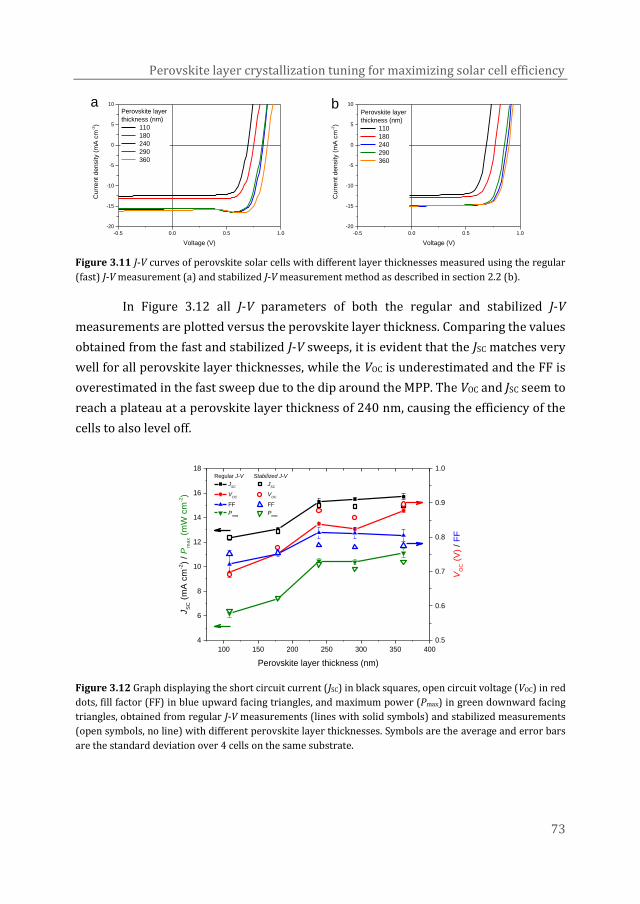
Perovskite layer crystallization tuning for maximizing solar cell efficiency
73
-0.5 0.0 0.5 1.0
-20
-15
-10
-5
0
5
10
Perovskite layer
thickness (nm)
110
180
240
290
360
Cu
rre
nt
de
nsity (
mA
cm
-2)
Voltage (V)
a
-0.5 0.0 0.5 1.0
-20
-15
-10
-5
0
5
10bPerovskite layer
thickness (nm)
110
180
240
290
360
Cu
rre
nt
de
nsity (
mA
cm
-2)
Voltage (V)
Figure 3.11 J-V curves of perovskite solar cells with different layer thicknesses measured using the regular
(fast) J-V measurement (a) and stabilized J-V measurement method as described in section 2.2 (b).
In Figure 3.12 all J-V parameters of both the regular and stabilized J-V
measurements are plotted versus the perovskite layer thickness. Comparing the values
obtained from the fast and stabilized J-V sweeps, it is evident that the JSC matches very
well for all perovskite layer thicknesses, while the VOC is underestimated and the FF is
overestimated in the fast sweep due to the dip around the MPP. The VOC and JSC seem to
reach a plateau at a perovskite layer thickness of 240 nm, causing the efficiency of the
cells to also level off.
100 150 200 250 300 350 400
4
6
8
10
12
14
16
18Regular J-V Stabilized J-V
JSC
JSC
VOC
VOC
FF FF
Pmax
Pmax
Perovskite layer thickness (nm)
JS
C (
mA
cm
-2)
/ P
max (
mW
cm
-2)
0.5
0.6
0.7
0.8
0.9
1.0
VO
C (
V)
/ F
F
Figure 3.12 Graph displaying the short circuit current (JSC) in black squares, open circuit voltage (VOC) in red
dots, fill factor (FF) in blue upward facing triangles, and maximum power (Pmax) in green downward facing
triangles, obtained from regular J-V measurements (lines with solid symbols) and stabilized measurements
(open symbols, no line) with different perovskite layer thicknesses. Symbols are the average and error bars
are the standard deviation over 4 cells on the same substrate.
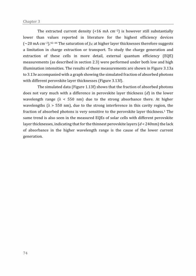
Chapter 3
74
The extracted current density (<16 mA cm−2) is however still substantially
lower than values reported in literature for the highest efficiency devices
(~20 mA cm−2).42–44 The saturation of JSC at higher layer thicknesses therefore suggests
a limitation in charge extraction or transport. To study the charge generation and
extraction of these cells in more detail, external quantum efficiency (EQE)
measurements (as described in section 2.3) were performed under both low and high
illumination intensities. The results of these measurements are shown in Figure 3.13a
to 3.13e accompanied with a graph showing the simulated fraction of absorbed photons
with different perovskite layer thicknesses (Figure 3.13f).
The simulated data (Figure 1.13f) shows that the fraction of absorbed photons
does not vary much with a difference in perovskite layer thickness (d) in the lower
wavelength range (λ < 550 nm) due to the strong absorbance there. At higher
wavelengths (λ > 550 nm), due to the strong interference in this cavity region, the
fraction of absorbed photons is very sensitive to the perovskite layer thickness.1 The
same trend is also seen in the measured EQEs of solar cells with different perovskite
layer thicknesses, indicating that for the thinnest perovskite layers (d < 240nm) the lack
of absorbance in the higher wavelength range is the cause of the lower current
generation.
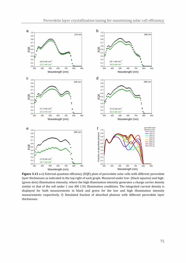
Perovskite layer crystallization tuning for maximizing solar cell efficiency
75
300 400 500 600 700 800 9000.0
0.1
0.2
0.3
0.4
0.5
0.6
0.7
0.8
0.9
1.0
14.0 mA cm-2
13.2 mA cm-2
EQ
E
Wavelength (nm)
110 nm
a
300 400 500 600 700 800 9000.0
0.1
0.2
0.3
0.4
0.5
0.6
0.7
0.8
0.9
1.0
15.7 mA cm-2
14.0 mA cm-2
EQ
E
Wavelength (nm)
180 nm
b
300 400 500 600 700 800 9000.0
0.1
0.2
0.3
0.4
0.5
0.6
0.7
0.8
0.9
1.0
17.2 mA cm-2
15.5 mA cm-2
EQ
E
Wavelength (nm)
240 nm
c
300 400 500 600 700 800 9000.0
0.1
0.2
0.3
0.4
0.5
0.6
0.7
0.8
0.9
1.0
17.5 mA cm-2
15.4 mA cm-2
EQ
E
Wavelength (nm)
290 nm
d
300 400 500 600 700 800 9000.0
0.1
0.2
0.3
0.4
0.5
0.6
0.7
0.8
0.9
1.0
17.8 mA cm-2
10.7 mA cm-2
EQ
E
Wavelength (nm)
360 nm
e
300 400 500 600 700 800 9000.0
0.1
0.2
0.3
0.4
0.5
0.6
0.7
0.8
0.9
1.0
Fra
ction o
f absorb
ed p
hoto
ns
Wavelength (nm)
perovskite layer
thickness (nm)
110 nm
145 nm
180 nm
210 nm
240 nm
290 nm
360 nm
475 nm
f
Figure 3.13 a-e) External quantum efficiency (EQE) plots of perovskite solar cells with different perovskite
layer thicknesses as indicated in the top right of each graph. Measured under low- (black squares) and high-
(green dots) illumination intensity, where the high illumination intensity generates a charge carrier density
similar to that of the cell under 1 sun AM 1.5G illumination conditions. The integrated current density is
displayed for both measurements in black and green for the low and high illumination intensity
measurements respectively. f) Simulated fraction of absorbed photons with different perovskite layer
thicknesses.

Chapter 3
76
The EQE and corresponding integrated current density obtained from the EQE
measurements at low light intensity increase significantly up to a layer thickness of
240 nm due to the increased absorbance. For thicker perovskite layers it increases only
marginally, which matches the results obtained in the stabilized J-V measurements.
However, the integrated current density from the low light intensity EQE
measurements is substantially larger than the one measured in the stabilized J-V
measurements, especially for the thickest layers. The reason for this difference becomes
clear when looking at the EQE of the cells measured at a high light intensity that
generates a charge carrier density similar to that of the cell in 1 sun AM 1.5G
illumination intensity. All EQEs measured at high light intensity are lower than those
measured at low light intensity. The striking observation here is that the difference
between the low- and high light intensity EQEs increases with the thickness of the
perovskite layer is. Indicating that charge transport and/or extraction is less efficient
for the thicker perovskite layers and that with all perovskite layers, the generated
photocurrent is increasing sublinear with the light intensity. It must be noted here that
only for the thickest perovskite cell (360 nm perovskite layer) the high light intensity
EQE measurement was performed using a much higher light intensity than for the
others. Explaining the much larger drop in EQE compared to the other samples and
showing that the effect is more severe at higher light intensity
In order to investigate this sublinear behavior of the photocurrent with respect
to the light intensity, the photocurrent was measured at different light intensities as
described in section 2.4. Figure 3.14 shows the ISC and EQE of the cells at a wavelength
of 530 nm plotted versus light intensity. The EQE is normalized to 1 at the lowest
measured light intensity. The light intensity dependent EQE measurements show that
the EQE is stable up to a photon flux of about 1016 cm−2 s−1, but starts dropping at higher
photon fluxes for all perovskite layer thicknesses. This reduction of EQE at high light
intensity is more severe with increasing perovskite layer thickness and it is the main
cause for the limitation of the solar cell performance.
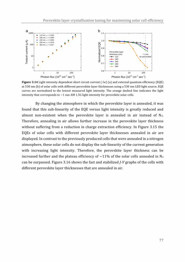
Perovskite layer crystallization tuning for maximizing solar cell efficiency
77
1 10 100
1
10
100
1000 110 nm, = 0.993
180 nm, = 0.985
240 nm, = 0.984
290 nm, = 0.978
360 nm, = 0.927
Te
stc
el cu
rre
nt
(A
)
Photon flux (1015
cm-2 sec
-1)
a
1 10 1000.6
0.7
0.8
0.9
1.0
1.1
Perovskite layer
thickness (nm)
110
180
240
290
360
~1 sun
for perovskite
Norm
aliz
ed E
QE
Photon flux (1015
cm-2 sec
-1)
b
Figure 3.14 Light intensity dependent short circuit current (Isc) (a) and external quantum efficiency (EQE)
at 530 nm (b) of solar cells with different perovskite layer thicknesses using a 530 nm LED light source. EQE
curves are normalized to the lowest measured light intensity. The orange dashed line indicates the light
intensity that corresponds to ~1 sun AM 1.5G light intensity for perovskite solar cells.
By changing the atmosphere in which the perovskite layer is annealed, it was
found that this sub-linearity of the EQE versus light intensity is greatly reduced and
almost non-existent when the perovskite layer is annealed in air instead of N2.
Therefore, annealing in air allows further increase in the perovskite layer thickness
without suffering from a reduction in charge extraction efficiency. In Figure 3.15 the
EQEs of solar cells with different perovskite layer thicknesses annealed in air are
displayed. In contrast to the previously produced cells that were annealed in a nitrogen
atmosphere, these solar cells do not display the sub-linearity of the current generation
with increasing light intensity. Therefore, the perovskite layer thickness can be
increased further and the plateau efficiency of ~11% of the solar cells annealed in N2
can be surpassed. Figure 3.16 shows the fast and stabilized J-V graphs of the cells with
different perovskite layer thicknesses that are annealed in air.
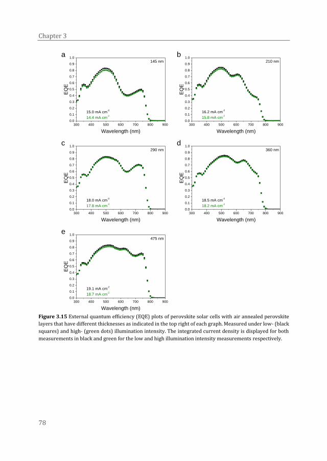
Chapter 3
78
300 400 500 600 700 800 9000.0
0.1
0.2
0.3
0.4
0.5
0.6
0.7
0.8
0.9
1.0
15.0 mA cm-2
14.4 mA cm-2
EQ
E
Wavelength (nm)
145 nm
a
300 400 500 600 700 800 9000.0
0.1
0.2
0.3
0.4
0.5
0.6
0.7
0.8
0.9
1.0
16.2 mA cm-2
15.8 mA cm-2
EQ
E
Wavelength (nm)
210 nm
b
300 400 500 600 700 800 9000.0
0.1
0.2
0.3
0.4
0.5
0.6
0.7
0.8
0.9
1.0
18.0 mA cm-2
17.8 mA cm-2
EQ
E
Wavelength (nm)
290 nm
c
300 400 500 600 700 800 9000.0
0.1
0.2
0.3
0.4
0.5
0.6
0.7
0.8
0.9
1.0
18.5 mA cm-2
18.2 mA cm-2
EQ
E
Wavelength (nm)
360 nm
d
300 400 500 600 700 800 9000.0
0.1
0.2
0.3
0.4
0.5
0.6
0.7
0.8
0.9
1.0
19.1 mA cm-2
18.7 mA cm-2
EQ
E
Wavelength (nm)
475 nm
e
Figure 3.15 External quantum efficiency (EQE) plots of perovskite solar cells with air annealed perovskite
layers that have different thicknesses as indicated in the top right of each graph. Measured under low- (black
squares) and high- (green dots) illumination intensity. The integrated current density is displayed for both
measurements in black and green for the low and high illumination intensity measurements respectively.
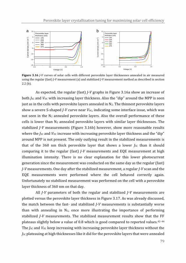
Perovskite layer crystallization tuning for maximizing solar cell efficiency
79
-0.5 0.0 0.5 1.0
-20
-15
-10
-5
0
5
10aC
urr
ent
de
nsity (
mA
cm
-2)
Voltage (V)
145
209
290
360
475
Perovskite layer
thickness (nm)
-0.5 0.0 0.5 1.0
-20
-15
-10
-5
0
5
10b
Cu
rre
nt
de
nsity (
mA
cm
-2)
Voltage (V)
Perovskite layer
thickness (nm)
145
209
290
360
475
Figure 3.16 J-V curves of solar cells with different perovskite layer thicknesses annealed in air measured
using the regular (fast) J-V measurement (a) and stabilized J-V measurement method as described in section
2.2 (b).
As expected, the regular (fast) J-V graphs in Figure 3.16a show an increase of
both JSC and VOC with increasing layer thickness. Also the “dip” around the MPP is seen
just as in the cells with perovskite layers annealed in N2. The thinnest perovskite layers
show a severe S-shaped J-V curve near VOC, indicating some interface issue, which was
not seen in the N2 annealed perovskite layers. Also the overall performance of these
cells is lower than N2 annealed perovskite layers with similar layer thicknesses. The
stabilized J-V measurements (Figure 3.16b) however, show more reasonable results
where the JSC and VOC increase with increasing perovskite layer thickness and the “dip”
around MPP is not present. The only outlying result in the stabilized measurements is
that of the 360 nm thick perovskite layer that shows a lower JSC than it should
comparing it to the regular (fast) J-V measurements and EQE measurement at high
illumination intensity. There is no clear explanation for this lower photocurrent
generation since the measurement was conducted on the same day as the regular (fast)
J-V measurements. One day after the stabilized measurement, a regular J-V scan and the
EQE measurements were performed where the cell behaved correctly again.
Unfortunately no stabilized measurement was performed on the cell with a perovskite
layer thickness of 360 nm on that day.
All J-V parameters of both the regular and stabilized J-V measurements are
plotted versus the perovskite layer thickness in Figure 3.17. As was already discussed,
the match between the fast- and stabilized J-V measurements is substantially worse
than with annealing in N2, once more illustrating the importance of performing
stabilized J-V measurements. The stabilized measurement results show that the FF
plateaus slightly below a value of 0.8 which is good compared to reported values.42–44
The JSC and VOC keep increasing with increasing perovskite layer thickness without the
JSC plateauing at high thicknesses like it did for the perovskite layers that were annealed

Chapter 3
80
in N2. This also causes Pmax to keep increasing with increasing perovskite layer thickness
and reaching the highest efficiency with the thickest perovskite layer of the series. The
calculated PCE of the solar cell with a perovskite layer of 475 nm thick is 14.2% (Table
3.1). It must be noted here that while the maximum PCE was obtained with the thickest
perovskite layer in the series, increasing the thickness further in subsequent
experiments resulted in lower solar cell efficiencies due to a reduction in JSC, VOC, and
FF.
100 150 200 250 300 350 400 450 500
2
4
6
8
10
12
14
16
18
20
Regular J-V Stabilized J-V
JSC
JSC
VOC
VOC
FF FF
Pmax
Pmax
Perovskite layer thickness (nm)
JS
C (
mA
cm
-2)
/ P
max (
mW
cm
-2)
0.5
0.6
0.7
0.8
0.9
1.0
VO
C (
V)
/ F
F
Figure 3.17 Graph displaying the short circuit current density (JSC) in black squares, open circuit voltage (VOC)
in red dots, fill factor (FF) in blue upward facing triangles, and maximum power (Pmax) in green downward
facing triangles, obtained from regular (fast) J-V measurements (lines with solid symbols) and stabilized
measurements (open symbols, no line) with different perovskite layer thicknesses that were annealed in air.
Symbols are the average and error bars are the standard deviation over 4 cells on the same substrate.
Table 3.1 Stabilized J-V parameters of solar cells with perovskite layers of different thicknesses (d) that were
annealed in air. The PCE is calculated by multiplying the VOC and FF obtained from the stabilized J-V sweep
with the JSC obtained from the high illumination intensity (light-biased) EQE measurement.
d (nm) JSC, stab
(mA cm−2)
VOC, stab
(V)
FF stab Pmax, stab
(mW cm−2)
JSC, SR
(mA cm−2)
JSC, SR bias
(mA cm−2)
PCE
(%)
145 13.5 0.93 0.73 8.9 15.0 14.4 9.7
209 13.9 0.95 0.76 10.0 16.2 15.8 11.9
290 15.8 0.95 0.75 11.2 18.0 17.8 12.6
361 13.6 0.95 0.76 9.9 18.5 18.2 13.2
475 17.9 0.98 0.78 13.6 19.1 18.7 14.2
Perovskite layer crystallization tuning for maximizing solar cell efficiency
81
3.6 Conclusions
In this chapter we have optimized methylammonium lead triiodide
(CH3NH3PbI3, MAPbI3) perovskite layers for use in planar p-i-n solar cells with
PEDOT:PSS and PCBM as hole and electron transporting layers respectively. By using
multiple lead sources (PbCl2 and Pb(OAc)2·3H2O) in the precursor mixture, and
changing the ratio between them, the crystallization process of the perovskite can be
controlled. This allows fine-tuning of the crystallization speed and with that the size of
the formed crystallites and the compactness of the perovskite layer, which are of great
influence on the solar cell performance. Additionally, the use of this precursor solution
composition results in an improved reproducibility compared to the “mixed halide”
mixture. An optimal perovskite layer morphology was found at PbCl2 and
Pb(OAc)2·3H2O fractions of 0.2 and 0.8 respectively, employing a 3:1 MAI:total Pb ratio
in DMF. The annealing time and temperature were also found to be critical parameters
for the formation of the desired perovskite layer, where annealing too long or too hot
leads to decomposition of the perovskite into PbI2 and MAI(g), while annealing too short
or too cold results in residual solvent or unreacted ions in the layer. Both of which were
found to be detrimental for solar cell performance. The optimal annealing time and
temperature that were found were 15 minutes and 90 °C respectively. The perovskite
layer thickness was found to have a significant influence on mainly the current density
that can be extracted from the solar cell, where an optimal layer thickness of 475nm
was found to yield a JSC of almost 18 mA cm−2. Additionally, it was found that these high
values of JSC could only be obtained by annealing the perovskite layer in ambient
conditions, since perovskite layers annealed in inert conditions suffer from strong
sublinearity of the photocurrent with illumination intensity. The cause of the reduction
in extracted photocurrent at high illumination intensities of solar cells annealed in N2
and why this is solved by annealing in air is discussed in detail in chapter 4 of this
dissertation. Finally, the optimized production procedure described in this chapter
allows the reproducible production of perovskite solar cells with an efficiency of ~14%.

Chapter 3
82
3.7 Experimental
Device fabrication:
Tin doped indium oxide (indium-tin oxide, ITO) coated and pre-patterned glass
substrates (Naranjo substrates) were cleaned by sonication in acetone (Sigma Aldrich),
scrubbing in a solution of sodium dodecyl sulfate (SDS, Acros, 99%) in filtered water
(Milli-Q), rinsing in deionized water, sonication in 2-propanol (Sigma Aldrich) and 30
minutes of UV-ozone treatment right before use. Poly(3,4-
ethylenedioxythiophene):poly(styrenesulfonate) (PEDOT:PSS, Heraeus Clevios PVP Al
4083) was filtered using a 0.45 µm PVDF filter and spin coated (40 sec, 3000 RPM) onto
the cleaned and UV-ozone treated substrates. The PEDOT:PSS layer is then dried at
140 °C for 15 minutes in ambient conditions.
For the perovskite precursor solutions methylammonium iodide (MAI)
(Dyesol), lead(II) chloride (PbCl2) (Sigma Aldrich, 98%), lead(II) acetate trihydrate
(Pb(OAc)2·3H2O, Sigma Aldrich, 99.999% trace metal basis), and
N,N-dimethylformamide (DMF, Sigma Aldrich, anhydrous, 99.8%) were used and the
solutions were stirred at room temperature until completely dissolved. The perovskite
precursor solution used in section 3.2 consisted of 450 mg mL−1 (MAI) and 233 mg mL−1
PbCl2 in DMF and was spin coated at 3000 RPM for 120 seconds. The formed film was
dried using ramp annealing which consisted of 1h at 25 °C, a ramp from 25 °C ⟶100 °C
at 1°C min−1 and 2 h at 100 °C in N2. For the production of the perovskite precursor
solutions used in section 3.3 two stock solutions were produced, one consisting of 450
mg mL−1 MAI and 232 mg mL−1 PbCl2 in DMF (solution I) and the other consisting of 450
mg mL−1 MAI and 319 mg mL−1 Pb(OAc)2·3H2O in DMF (solution II). To make solutions
with different ratios, the two stock solutions were mixed in (I:II) 1:9, 1:4, 3:7, 2:3, 1:1,
3:2, and 7:3 ratio for fractions of 0.1, 0.2, 0.3, 0.4, 0.5, 0.6, and 0.7 PbCl2 respectively. All
solutions were spin coated at 3000 RPM for 60 seconds. The formed films were
annealed for 10 min at 130 °C in N2. The perovskite precursor solution used in section
3.4 was produced in the same way as those used for section 3.3 (fraction PbCl2 = 0.2)
and was spin coated at 3000 RPM for 120 seconds. The formed films were annealed for
10 min at 70, 90, 110, and 130 °C, and for 30 min at 90 and 110 °C in N2. The perovskite
precursor solutions used in the first part (N2 annealing) of section 3.5 consisted of 287,
383, 481, 574, and 670 mg mL−1 MAI; 34, 45, 54, 66, and 76 mg mL−1 PbCl2; and 182,
243, 302, 364, and 425 mg mL−1 Pb(OAc)2·3H2O in DMF for perovskite layer thicknesses
of 110, 180, 240, 290, and 360 nm respectively. The precursor solutions were spin
coated at 5700 RPM for 120 seconds and the formed films were annealed for 10 min at
Perovskite layer crystallization tuning for maximizing solar cell efficiency
83
90 °C in N2. The perovskite precursor solutions used in the second part (air annealing)
of section 3.5 were diluted from a stock solution containing 952 mg mL−1 MAI, 110 mg
mL−1 PbCl2 and 609 mg mL−1 Pb(OAc)2·3H2O in DMF. From this stock solution, 50 µL
was taken and 5.6, 12.5, 21.4, 33.3, and 50 µL of DMF was added for perovskite layer
thicknesses of 475, 360, 290, 210 and 145 nm respectively. The precursor solutions
were spin coated at 5700 RPM for 120 seconds and the formed films were annealed for
15 min at 90 °C in air.
For the electron transport layer (ETL), 24 mg mL−1 of [6,6]-phenyl-C61-butyric
acid methyl ester (PCBM, Solenne BV, 99%) was dissolved in a 50/50 mixture of
chloroform (Biosolve, AR grade) and chlorobenzene (Sigma Aldrich, anhydrous 99.8%)
and spin coated on top of the completed perovskite layer (60 s at 500 RPM) in the same
atmosphere as where the cells are annealed. After that, the contact area was cleaned
and LiF (1 nm) and Al (100 nm) were thermally evaporated under high vacuum
(±3×10⁻⁷ mbar) as a back electrode.
Measurement methods:
Layer thicknesses were measured using a Veeco Dektak 150 profilometer.
J–V characteristics were measured in a nitrogen environment with a Keithley
2400 source meter under ±100 mW cm−2 white light illumination from a tungsten-
halogen lamp filtered by a Schott GG385 UV filter and a Hoya LB120 daylight filter. The
cells were masked with a 0.0676 cm2 or 0.1296 cm2 aperture (the physical overlap of
the contacts is 0.09 cm2 and 0.16 cm2 respectively). Regular (fast) upwards and
downwards J–V sweeps were performed between −0.5 and 1.5 V with a scan speed of
0.25 V s−1. The stabilized J-V measurement protocol (section 2.3) used was defined by
light soaking at VOC for 10 minutes, followed by a downward sweep (VOC + 0.05 V →
−0.05 V) with a step size of 0.025 V.
Short-circuit currents under AM 1.5G conditions were determined by
integrating the spectral response with the solar spectrum. Spectral response
measurements were conducted under only probe light and 1 sun operating conditions
by using a 530 nm high power LED (Thorlabs M530L3 driven by a DC4104 driver) for
bias illumination. The device was kept in a nitrogen filled box behind a quartz window
and a circular aperture with a 1 mm radius and irradiated with modulated
monochromatic light, from a 50 W tungsten-halogen lamp (Philips focusline) and
monochromator (Oriel, Cornerstone 130) with the use of a mechanical chopper (160
Hz). The response was recorded as a voltage from a preamplifier (SR570) using a lock-
in amplifier (SR830). A calibrated silicon cell was used as reference (calibrated at the
Energy research Centre of the Netherlands).

Chapter 3
84
JSC and VOC vs light intensity measurements were performed using a Keithley
2400 source meter and 405 and 730 nm high power LEDs (Thorlabs M405L3 and
M730L4 driven by a DC4104 driver) for illumination.
Scanning electron microscopy (SEM) was performed on a FEI Quanta 3D FEG.
JSC, EQE, and VOC vs light intensity measurements were performed using a
Keithley 2400 source meter and 730 nm high power LEDs (Thorlabs M730L4 driven by
a DC4104 driver) for illumination.
X-Ray Diffraction measurements were performed on a Bruker 2D Phaser using
Cu Kα radiation with a wavelength of 0.15406 nm between 2θ angles of 10 to 60° using
increments of 0.05° and a 2 second integration time. A 0.6 mm slit was used at the X-
Ray source and a shield was positioned 0.5 mm above the sample surface. The sample
rotated at a speed of 60 RPM during the measurement.
Optical Modeling
Optical modeling based on the TM method was performed using Setfos 4.3
(Fluxim). The solar cell stack used consisted of glass (100nm, incoherent), SiO2 (20 nm),
ITO (140 nm), PEDOT:PSS (40 nm) perovskite (variable thickness), PCBM (110 nm), LiF
(1 nm), and Al (100 nm).

Perovskite layer crystallization tuning for maximizing solar cell efficiency
85
3.8 References
1 Q. Lin, A. Armin, R. C. R. Nagiri, P. L. Burn and P. Meredith, Nat. Photonics, 2014, 9, 106–
112.
2 N. G. Park, Mater. Today, 2015, 18, 65–72.
3 C. Wehrenfennig, G. E. Eperon, M. B. Johnston, H. J. Snaith and L. M. Herz, Adv. Mater., 2014,
26, 1584–1589.
4 C.-S. Jiang, M. Yang, Y. Zhou, B. To, S. U. Nanayakkara, J. M. Luther, W. Zhou, J. J. Berry, J.
van de Lagemaat, N. P. Padture, K. Zhu and M. M. Al-Jassim, Nat. Commun., 2015, 6, 8397.
5 V. D‘Innocenzo, G. Grancini, M. J. P. Alcocer, A. R. S. Kandada, S. D. Stranks, M. M. Lee, G.
Lanzani, H. J. Snaith and A. Petrozza, Nat. Commun., 2014, 5, 1–6.
6 G. E. Eperon, S. D. Stranks, C. Menelaou, M. B. Johnston, L. M. Herz and H. J. Snaith, Energy
Environ. Sci., 2014, 7, 982.
7 G. E. Eperon, G. M. Paterno, R. J. Sutton, A. Zampetti, A. A. Haghighirad, F. Cacialli and H. J.
Snaith, J. Mater. Chem. A, 2015, 3, 19688–19695.
8 W. Zhang, M. Saliba, D. T. Moore, S. K. Pathak, M. T. Hörantner, T. Stergiopoulos, S. D.
Stranks, G. E. Eperon, J. A. Alexander-Webber, A. Abate, A. Sadhanala, S. Yao, Y. Chen, R. H.
Friend, L. A. Estroff, U. Wiesner and H. J. Snaith, Nat. Commun., 2015, 6, 6142.
9 N. J. Jeon, J. H. Noh, Y. C. Kim, W. S. Yang, S. Ryu and S. Il Seok, Nat. Mater., 2014, 13, 897–
903.
10 N. K. Noel, S. N. Habisreutinger, B. Wenger, M. T. Klug, M. T. Hörantner, M. B. Johnston, R.
J. Nicholas, D. T. Moore and H. J. Snaith, Energy Environ. Sci., 2017, 10, 145-152.
11 K. Hendriks, J. J. van Franeker, B. J. Bruijnaers, J. A. Anta, M. M. Wienk and R. A. J. Janssen,
J. Mater. Chem. A., 2017, 5, 2346-2354.
12 W. Liao, D. Zhao, Y. Yu, N. Shrestha, K. Ghimire, C. R. Grice, C. Wang, Y. Xiao, A. J. Cimaroli,
R. J. Ellingson, N. J. Podraza, K. Zhu, R.-G. Xiong and Y. Yan, J. Am. Chem. Soc., 2016, 138,
12360–12363.
13 H.-B. Kim, H. Choi, J. Jeong, S. Kim, B. Walker, S. Song and J. Y. Kim, Nanoscale, 2014, 6,
6679-6683.
14 W. Qiu, T. Merckx, M. Jaysankar, C. Masse de la Huerta, L. Rakocevic, W. Zhang, U. W.
Paetzold, R. Gehlhaar, L. Froyen, J. Poortmans, D. Cheyns, H. J. Snaith and P. Heremans,
Energy Environ. Sci., 2016, 9, 484–489.
15 F. K. Aldibaja, L. Badia, E. Mas-Marzá, R. S. Sánchez, E. M. Barea and I. Mora-Sero, J. Mater.
Chem. A, 2015, 3, 9194–9200.
16 J. Qing, H.-T. Chandran, Y.-H. Cheng, X.-K. Liu, H.-W. Li, S.-W. Tsang, M.-F. Lo and C.-S. Lee,
Appl. Mater. Interfaces, 2015, 7, 23110–23116.
17 J. H. Heo, S. H. Im, J. H. Noh, T. N. Mandal, C.-S. Lim, J. A. Chang, Y. H. Lee, H. Kim, A. Sarkar,
M. K. Nazeeruddin, M. Grätzel and S. Il Seok, Nat. Photonics, 2013, 7, 486–491.
18 M. Liu, M. B. Johnston and H. J. Snaith, Nature, 2013, 501, 395–398.
Chapter 3
86
19 P.-W. Liang, C.-Y. Liao, C.-C. Chueh, F. Zuo, S. T. Williams, X.-K. Xin, J. Lin and A. K.-Y. Jen,
Adv. Mater., 2014, 26, 3748–3754.
20 D. Liu and T. L. Kelly, Nat. Photonics, 2013, 8, 133–138.
21 J. You, Z. Hong, Y. Yang, Q. Chen, M. Cai, T.-B. Song, C.-C. Chen, S. Lu, Y. Liu, H. Zhou and Y.
Yang, ACS Nano, 2014, 8, 1674–1680.
22 O. Malinkiewicz, A. Yella, Y. H. Lee, G. M. Espallargas, M. Graetzel, M. K. Nazeeruddin and
H. J. Bolink, Nat. Photonics, 2014, 8, 128–132.
23 Q. Chen, H. Zhou, Z. Hong, S. Luo, H.-S. Duan, H.-H. Wang, Y. Liu, G. Li and Y. Yang, J. Am.
Chem. Soc., 2013, 136, 622–625.
24 V. Gonzalez-Pedro, E. J. Juarez-Perez, W.-S. Arsyad, E. M. Barea, F. Fabregat-Santiago, I.
Mora-Sero and J. Bisquert, Nano Lett., 2014, 14, 888–893.
25 G. E. Eperon, V. M. Burlakov, A. Goriely and H. J. Snaith, ACS Nano, 2014, 8, 591–598.
26 C. Roldán-Carmona, O. Malinkiewicz, A. Soriano, G. Mínguez Espallargas, A. Garcia, P.
Reinecke, T. Kroyer, M. I. Dar, M. K. Nazeeruddin and H. J. Bolink, Energy Environ. Sci.,
2014, 7, 994.
27 G. E. Eperon, V. M. Burlakov, P. Docampo, A. Goriely and H. J. Snaith, Adv. Funct. Mater.,
2014, 24, 151–157.
28 S. D. Stranks, G. E. Eperon, G. Grancini, C. Menelaou, M. J. P. Alcocer, T. Leijtens, L. M. Herz,
A. Petrozza and H. J. Snaith, Science, 2014, 342, 341–344.
29 Q. Chen, H. Zhou, Y. Fang, A. Z. Stieg, T.-B. Song, H.-H. Wang, X. Xu, Y. Liu, S. Lu, J. You, P.
Sun, J. McKay, M. S. Goorsky and Y. Yang, Nat. Commun., 2015, 6, 7269.
30 S. Colella, E. Mosconi, G. Pellegrino, A. Alberti, V. L. P. Guerra, S. Masi, A. Listorti, A. Rizzo,
G. G. Condorelli, F. De Angelis and G. Gigli, J. Phys. Chem. Lett., 2014, 5, 3532–3538.
31 H. Yu, F. Wang, F. Xie, W. Li, J. Chen and N. Zhao, Adv. Funct. Mater., 2014, 24, 7102–7108.
32 S. Colella, E. Mosconi, P. Fedeli, A. Listorti, F. Gazza, F. Orlandi, P. Ferro, T. Besagni, A. Rizzo,
G. Calestani, G. Gigli, F. De Angelis and R. Mosca, Chem. Mater., 2013, 25, 4613–4618.
33 T. A. Berhe, W.-N. Su, C.-H. Chen, C.-J. Pan, J.-H. Cheng, H.-M. Chen, M.-C. Tsai, L.-Y. Chen, A.
A. Dubale and B.-J. Hwang, Energy Environ. Sci., 2016, 9, 323–356.
34 Takeo Oku, Solar Cells - New Approaches and Reviews, chapter 3, 2015.
35 S. Bae, J.-S. Park, I. K. Han, T. J. Shin and W. H. Jo, Sol. Energy Mater. Sol. Cells, 2017, 160,
77–84.
36 P. Docampo, F. C. Hanusch, N. Giesbrecht, P. Angloher, A. Ivanova, T. Bein, APL Mater.,
2014, 2, 81508.
37 B. J. Foley, J. Girard, B. A. Sorenson, A. Z. Chen, J. S. Niezgoda, M. R. Alpert, A. F. Harper, D.-
M. Smilgies, P. Clancy, W. A. Saidi and J. J. Choi, J. Mater. Chem. A, 2017, 5, 113–123.
38 A. Z. Chen, B. J. Foley, J. H. Ma, M. R. Alpert, J. S. Niezgoda and J. J. Choi, J. Mater. Chem. A,
2017, 5, 7796–7800.
39 Q. Dong, Y. Yuan, Y. Shao, Y. Fang, Q. Wang and J. Huang, Energy Environ. Sci., 2015, 8,
2464–2470.
Perovskite layer crystallization tuning for maximizing solar cell efficiency
87
40 W. Zhu, C. Bao, B. Lv, F. Li, Y. Yi, Y. Wang, J. Yang, X. Wang, T. Yu and Z. Zou, J. Mater. Chem.
A, 2016, 4, 12535–12542.
41 M. M. Lee, J. Teuscher, T. Miyasaka, T. N. Murakami, H. J. Snaith, Science, 2012, 338, 643-
647
42 S. S. Mali and C. K. Hong, Nanoscale, 2016, 8, 10528–10540.
43 C. Roldán-Carmona, O. Malinkiewicz, R. Betancur, G. Longo, C. Momblona, F. Jaramillo, L.
Camacho and H. J. Bolink, Energy Environ. Sci., 2014, 7, 2968–2973.
44 P. Docampo, J. M. Ball, M. Darwich, G. E. Eperon and H. J. Snaith, Nat. Commun., 2013, 4,
2761.
45 S. S. Shin, W. S. Yang, J. H. Noh, J. H. Suk, N. J. Jeon, J. H. Park, J. S. Kim, W. M. Seong and S. Il
Seok, Nat. Commun., 2015, 6, 7410.
46 J. H. Heo, M. H. Lee, H. J. Han, B. R. Patil, J. S. Yu and S. H. Im, J. Mater. Chem. A, 2016, 4,
1572–1578.

Chapter 4
The effect of oxygen on the
efficiency of planar p-i-n metal
halide perovskite solar cells
with a PEDOT:PSS hole
transport layer*
Abstract
Poly(3,4-ethylenedioxythiophene):poly(styrenesulfonate) (PEDOT:PSS) is
frequently used as hole transport layer in planar p-i-n perovskite solar cells. Here we
show that the processing of a metal halide perovskite layer on top of PEDOT:PSS via spin
coating of a precursor solution chemically reduces the oxidation state of PEDOT:PSS.
This reduction leads to a lowering of the work function of the PEDOT:PSS and the
perovskite layer on top of it. As a consequence, the solar cells display inferior
performance with a reduced open-circuit voltage and a reduced short-circuit current
density, which increases sublinearly with light intensity. The reduced PEDOT:PSS can be
re-oxidized by thermal annealing of the PEDOT:PSS/perovskite layer stack in the
presence of oxygen. As a consequence, thermal annealing of the perovskite layer in air
provides solar cells with increased open-circuit voltage, short-circuit current density and
high efficiency.
* This work has been published as: B. J. Bruijnaers, E. Schiepers, C. H. L. Weijtens,
S. C. J. Meskers, M. M. Wienk and R. A. J. Janssen, J. Mater. Chem. A, 2018, 6, 6822-6890

Chapter 4
90
4.1 Introduction
Metal halide perovskite materials currently attract great interest for use in
hybrid organic-inorganic solar cells. Methylammonium lead halides were first used in
2009 as light sensitizers of mesoporous titania (TiO2) in photovoltaic cells comprising
a liquid electrolyte, providing a power conversion efficiency (PCE) of 3.8%.1 The
introduction of a solid organic hole transport material efficiently solved the fast
degradation of the liquid-electrolyte cells and led to stable photovoltaic cells with an
optimized PCE of 9.7%.2 The use of an insulating alumina (Al2O3) layer instead of the
electron-transporting TiO2 layer proved that the perovskite material itself is capable
of free charge generation and very efficient ambipolar charge transport.3 Recent
advances have shown PCEs of over 22% for metal halide perovskites with optimized
compositions and processing methods.4,5
Many desirable properties like strong absorption, low exciton binding energy
for creating free charges6–8 and high charge mobilities and lifetimes9 characterize
metal halide perovskite materials. The fact that they can be processed from solution
with relative ease makes future roll-to-roll processing an attractive option.10–12 Their
versatility in composition and processing has allowed the usage of different solvents
and precursor materials and even made it possible to tune the band gap of the
material.13–23
Precursor and solvent combinations also allow changing of the morphology of
the perovskite layer by influencing nucleation and crystal growth during the
processing steps.24–27 The versatility in processing has led to many different
processing techniques ranging from single-step solution processing,4,18 to multi-step
solution processing with and without drying and anti-solvent treatments,28–31 single
and multi-step thermal evaporation and even combinations of solution processing and
thermal evaporation.32–36 After the deposition of the precursor materials, usually a
(thermal) annealing step is used to convert the deposited layer into the desired
perovskite phase and morphology.37–41 By changing the composition of the precursor
solution, the crystallization process can be retarded or sped up and by combining
different lead salt precursors, the layer can even be tuned to achieve a favorable
morphology and smoothness of the perovskite layer for the most efficient solar cells,
which is especially important in planar device configurations.24,26,42
Here we investigate the influence of the processing atmosphere on the
photovoltaic performance of planar p-i-n perovskite solar cells with poly(3,4-
ethylenedioxythiophene):poly(styrenesulfonate) (PEDOT:PSS) as hole transport layer,
The effect of oxygen on the efficiency of planar p-i-n metal halide perovskite solar cells with a PEDOT:PSS hole transport layer
91
methylammonium lead triiodide as semiconductor and [6,6]-phenyl-C61-butyric acid
methyl ester (PCBM) as electron transport layer. To do so, a processing method that
allows complete processing in ambient atmosphere was developed.
4.2 The effect of processing atmosphere on solar
cell performance
The perovskite solar cell fabrication is based on a triple anion solution of
methylammonium iodide (MAI), lead(II) chloride (PbCl2) and lead(II) acetate
trihydrate (Pb(OAc)2·3H2O) in N,N-dimethylformamide (DMF). This solution is heated
to 70 °C and spin coated dynamically onto a pre-heated (100 °C) glass substrate with
patterned indium tin oxide (ITO), covered with PEDOT:PSS. By this hot-casting
method the very hygroscopic precursor salts are already converted to the perovskite
during deposition, as indicated by a pronounced color change from the yellow
precursor to the brown perovskite. This allows the complete processing of the solar
cell in ambient atmosphere. Even though perovskite crystals are already formed
during casting, a short additional thermal annealing step, during which the color of the
perovskite layer changes from light brown to dark brown, is required to maximize the
efficiency.42 The devices are completed by a PCBM electron transport layer and a
LiF/Al top contact. Further details of the fabrication can be found in the experimental
section.
Figure 4.1a shows the stabilized current density-voltage (J−V) measurements
under simulated AM 1.5G (100 mW cm−2) illumination of these p-i-n photovoltaic
devices, when all processing steps are either done in ambient air or in an inert
atmosphere. The corresponding photovoltaic parameters are summarized in Table
4.1. Strikingly, the efficiency of cells processed under inert conditions (N2 atmosphere,
< 1 ppm O2 and < 1 ppm H2O) is much lower than the PCE of the air-processed devices
where both JSC and VOC are considerably enhanced.
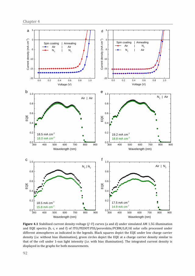
Chapter 4
92
0.0 0.2 0.4 0.6 0.8 1.0-20
-15
-10
-5
0
5
Spin coating | Annealing
Air | Air
N2 | N
2
Curr
ent density (
mA
cm
-2)
Voltage (V)
a
0.0 0.2 0.4 0.6 0.8 1.0
-20
-15
-10
-5
0
5
Spin coating | Annealing
Air | N2
N2 | Air
Cu
rren
t de
nsity (
mA
cm
-2)
Voltage (V)
d
300 400 500 600 700 800 9000.0
0.2
0.4
0.6
0.8
1.0
18.5 mA cm-2
18.0 mA cm-2
Air | Air
EQ
E
Wavelength (nm)
b
300 400 500 600 700 800 9000.0
0.2
0.4
0.6
0.8
1.0
19.2 mA cm-2
18.8 mA cm-2
N2 | Air
EQ
E
Wavelength (nm)
e
300 400 500 600 700 800 9000.0
0.2
0.4
0.6
0.8
1.0
18.5 mA cm-2
15.8 mA cm-2
N2 | N
2
EQ
E
Wavelength (nm)
c
300 400 500 600 700 800 9000.0
0.2
0.4
0.6
0.8
1.0
17.5 mA cm-2
14.9 mA cm-2
Air | N2
EQ
E
Wavelength (nm)
f
Figure 4.1 Stabilized current density-voltage (J−V) curves (a and d) under simulated AM 1.5G illumination
and EQE spectra (b, c, e and f) of ITO/PEDOT:PSS/perovskite/PCBM/LiF/Al solar cells processed under
different atmospheres as indicated in the legends. Black squares depict the EQE under low charge carrier
density (i.e. without bias illumination), green circles depict the EQE at a charge carrier density similar to
that of the cell under 1-sun light intensity (i.e. with bias illumination). The integrated current density is
displayed in the graphs for both measurements.
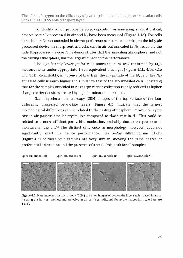
The effect of oxygen on the efficiency of planar p-i-n metal halide perovskite solar cells with a PEDOT:PSS hole transport layer
93
To identify which processing step, deposition or annealing, is most critical,
devices partially processed in air and N2 have been measured (Figure 4.1d). For cells
deposited in N2 but annealed in air the performance is almost identical to the fully air
processed device. In sharp contrast, cells cast in air but annealed in N2, resemble the
fully N2-processed devices. This demonstrates that the annealing atmosphere, and not
the casting atmosphere, has the largest impact on the performance.
The significantly lower JSC for cells annealed in N2 was confirmed by EQE
measurements under appropriate 1-sun equivalent bias light (Figure 4.1b, 4.1c, 4.1e
and 4.1f). Remarkably, in absence of bias light the magnitude of the EQEs of the N2-
annealed cells is much higher and similar to that of the air-annealed cells. Indicating
that for the samples annealed in N2 charge carrier collection is only reduced at higher
charge carrier densities created by high illumination intensities.
Scanning electron microscopy (SEM) images of the top surface of the four
differently processed perovskite layers (Figure 4.2) indicate that the largest
morphological differences can be related to the casting atmosphere. Perovskite layers
cast in air possess smaller crystallites compared to those cast in N2. This could be
related to a more efficient perovskite nucleation, probably due to the presence of
moisture in the air.43 The distinct difference in morphology, however, does not
significantly affect the device performance. The X-Ray diffractograms (XRD)
(Figure 4.3) of these four samples are very similar, showing the same degree of
preferential orientation and the presence of a small PbI2 peak for all samples.
Spin: air, anneal: air Spin: air, anneal: N2 Spin: N2, anneal: air Spin: N2, anneal: N2
Figure 4.2 Scanning electron microscopy (SEM) top view images of perovskite layers spin coated in air or
N2 using the hot cast method and annealed in air or N2 as indicated above the images (all scale bars are
1 µm).
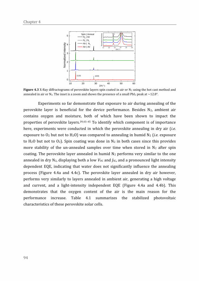
Chapter 4
94
10 20 30 40 50 60
0
1
2
3
4
5
11 12 13 14 15 16
No
rmaliz
ed
in
ten
sity
2()
Spin | Anneal
N2 | Air
N2 | N
2
Air | N2
Air | Air
(110) (220)
No
rma
lize
d in
tensity
2()
PbI2
Figure 4.3 X-Ray diffractograms of perovskite layers spin coated in air or N2 using the hot cast method and
annealed in air or N2. The inset is a zoom and shows the presence of a small PbI2 peak at ~12.8°.
Experiments so far demonstrate that exposure to air during annealing of the
perovskite layer is beneficial for the device performance. Besides N2, ambient air
contains oxygen and moisture, both of which have been shown to impact the
properties of perovskite layers.39,43–45 To identify which component is of importance
here, experiments were conducted in which the perovskite annealing in dry air (i.e.
exposure to O2 but not to H2O) was compared to annealing in humid N2 (i.e. exposure
to H2O but not to O2). Spin coating was done in N2 in both cases since this provides
more stability of the un-annealed samples over time when stored in N2 after spin
coating. The perovskite layer annealed in humid N2 performs very similar to the one
annealed in dry N2, displaying both a low VOC and JSC, and a pronounced light intensity
dependent EQE, indicating that water does not significantly influence the annealing
process (Figure 4.4a and 4.4c). The perovskite layer annealed in dry air however,
performs very similarly to layers annealed in ambient air, generating a high voltage
and current, and a light-intensity independent EQE (Figure 4.4a and 4.4b). This
demonstrates that the oxygen content of the air is the main reason for the
performance increase. Table 4.1 summarizes the stabilized photovoltaic
characteristics of these perovskite solar cells.
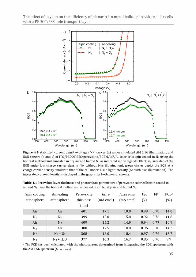
The effect of oxygen on the efficiency of planar p-i-n metal halide perovskite solar cells with a PEDOT:PSS hole transport layer
95
0.0 0.2 0.4 0.6 0.8 1.0-20
-15
-10
-5
0
5
Spin coating | Annealing
N2 | N
2 + H
2O
N2 | N
2 + O
2
Cu
rrent density (
mA
cm
-2)
Voltage (V)
a
300 400 500 600 700 800 9000.0
0.2
0.4
0.6
0.8
1.0
19.0 mA cm-2
18.4 mA cm-2
N2 | N
2 + O
2
EQ
E
Wavelength (nm)
b
300 400 500 600 700 800 9000.0
0.2
0.4
0.6
0.8
1.0
19.4 mA cm-2
16.7 mA cm-2
N2 | N
2 + H
2O
EQ
E
Wavelength (nm)
c
Figure 4.4 Stabilized current density-voltage (J−V) curves (a) under simulated AM 1.5G illumination, and
EQE spectra (b and c) of ITO/PEDOT:PSS/perovskite/PCBM/LiF/Al solar cells spin coated in N2 using the
hot cast method and annealed in dry air and humid N2 as indicated in the legends. Black squares depict the
EQE under low charge carrier density (i.e. without bias illumination), green circles depict the EQE at a
charge carrier density similar to that of the cell under 1-sun light intensity (i.e. with bias illumination). The
integrated current density is displayed in the graphs for both measurements.
Table 4.1 Perovskite layer thickness and photovoltaic parameters of perovskite solar cells spin coated in
air and N2 using the hot cast method and annealed in air, N2, dry air and humid N2.
Spin coating
atmosphere
Annealing
atmosphere
Perovskite
thickness
(nm)
JSC, J-V
(mA cm−2)
JSC, SR @ 1sun
(mA cm−2)
VOC
(V)
FF PCEa
(%)
Air Air 401 17.1 18.0 0.99 0.78 14.0
N2 N2 399 15.0 15.8 0.92 0.76 11.8
Air N2 409 15.2 14.9 0.94 0.77 10.9
N2 Air 380 17.5 18.8 0.96 0.78 14.2
N2 N2 + O2 368 18.0 18.4 0.97 0.76 13.7
N2 N2 + H2O 377 16.3 16.7 0.85 0.70 9.9 a The PCE has been calculated with the photocurrent determined from integrating the EQE spectrum with
the AM 1.5G spectrum (JSC, SR @ 1 sun).
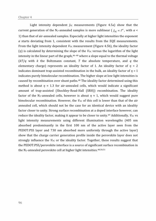
Chapter 4
96
Light intensity dependent JSC measurements (Figure 4.5a) show that the
current generation of the N2-annealed samples is more sublinear ( SCαJ I , with α <
1) than that of air-annealed samples. Especially at higher light intensities the exponent
α starts deviating from 1, consistent with the results from the EQE measurements.
From the light intensity dependent VOC measurement (Figure 4.5b), the ideality factor
(η) is calculated by determining the slope of the VOC versus the logarithm of the light
intensity in the linear part of the graph,46–48 where a slope equal to the thermal voltage
(kT/q with k the Boltzmann constant, T the absolute temperature, and q the
elementary charge) represents an ideality factor of 1. An ideality factor of η = 2
indicates dominant trap-assisted recombination in the bulk, an ideality factor of η = 1
indicates purely bimolecular recombination. The higher slope at low light intensities is
caused by recombination over shunt paths.48 The ideality factor determined using this
method is about η ≈ 1.3 for air-annealed cells, which would indicate a significant
amount of trap-assisted (Shockley-Read-Hall (SRH)) recombination. The ideality
factor of the N2-annealed cells, however is about η ≈ 1, which would suggest pure
bimolecular recombination. However, the VOC of this cell is lower than that of the air
annealed cell, which should not be the case for an identical device with an ideality
factor closer to unity. Strong surface recombination at a doped interface however, can
reduce the ideality factor, making it appear to be closer to unity.49 Additionally, VOC vs
light intensity measurements using different illumination wavelengths (405 nm
absorbed predominantly in the first 100 nm of the active layer seen from the
PEDOT:PSS layer and 730 nm absorbed more uniformly through the active layer)
show that the charge carrier generation profile inside the perovskite layer does not
strongly influence the VOC or the ideality factor. Together, these results suggest that
the PEDOT:PSS/perovskite interface is a source of significant surface recombination in
the N2-annealed perovskite cell at higher light intensities.48,50,51
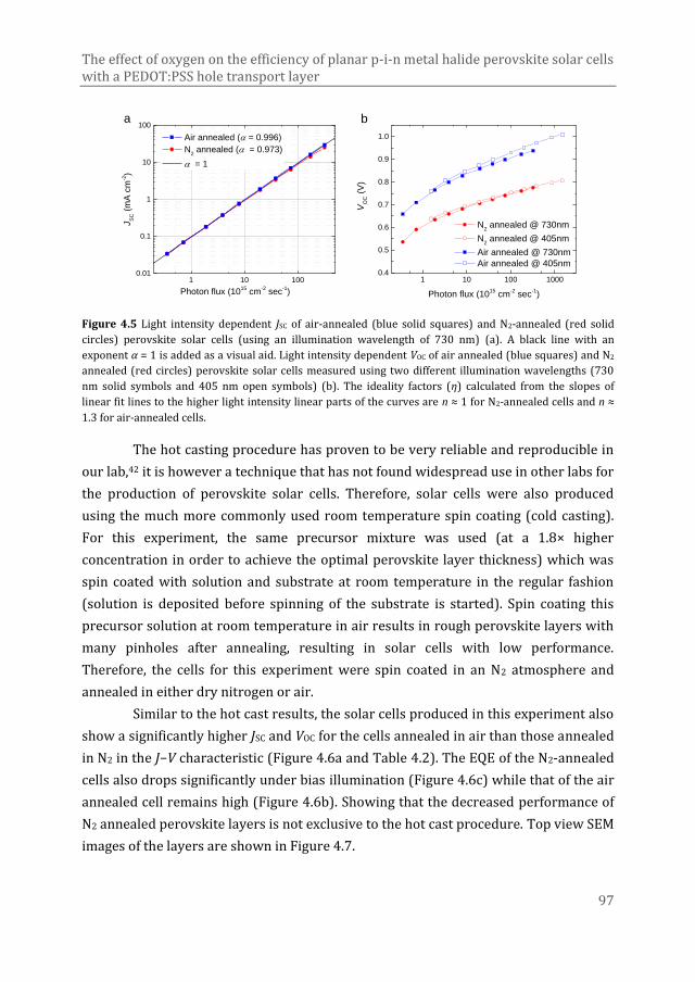
The effect of oxygen on the efficiency of planar p-i-n metal halide perovskite solar cells with a PEDOT:PSS hole transport layer
97
1 10 1000.01
0.1
1
10
100a
Photon flux (1015
cm-2 sec
-1)
JS
C (
mA
cm
-2)
Air annealed ( = 0.996)
N2 annealed ( = 0.973)
= 1
1 10 100 10000.4
0.5
0.6
0.7
0.8
0.9
1.0
VO
C (
V)
Photon flux (1015
cm-2 sec
-1)
N2 annealed @ 730nm
N2 annealed @ 405nm
Air annealed @ 730nm
Air annealed @ 405nm
b
Figure 4.5 Light intensity dependent JSC of air-annealed (blue solid squares) and N2-annealed (red solid
circles) perovskite solar cells (using an illumination wavelength of 730 nm) (a). A black line with an
exponent α = 1 is added as a visual aid. Light intensity dependent VOC of air annealed (blue squares) and N2
annealed (red circles) perovskite solar cells measured using two different illumination wavelengths (730
nm solid symbols and 405 nm open symbols) (b). The ideality factors (η) calculated from the slopes of
linear fit lines to the higher light intensity linear parts of the curves are n ≈ 1 for N2-annealed cells and n ≈
1.3 for air-annealed cells.
The hot casting procedure has proven to be very reliable and reproducible in
our lab,42 it is however a technique that has not found widespread use in other labs for
the production of perovskite solar cells. Therefore, solar cells were also produced
using the much more commonly used room temperature spin coating (cold casting).
For this experiment, the same precursor mixture was used (at a 1.8× higher
concentration in order to achieve the optimal perovskite layer thickness) which was
spin coated with solution and substrate at room temperature in the regular fashion
(solution is deposited before spinning of the substrate is started). Spin coating this
precursor solution at room temperature in air results in rough perovskite layers with
many pinholes after annealing, resulting in solar cells with low performance.
Therefore, the cells for this experiment were spin coated in an N2 atmosphere and
annealed in either dry nitrogen or air.
Similar to the hot cast results, the solar cells produced in this experiment also
show a significantly higher JSC and VOC for the cells annealed in air than those annealed
in N2 in the J−V characteristic (Figure 4.6a and Table 4.2). The EQE of the N2-annealed
cells also drops significantly under bias illumination (Figure 4.6c) while that of the air
annealed cell remains high (Figure 4.6b). Showing that the decreased performance of
N2 annealed perovskite layers is not exclusive to the hot cast procedure. Top view SEM
images of the layers are shown in Figure 4.7.
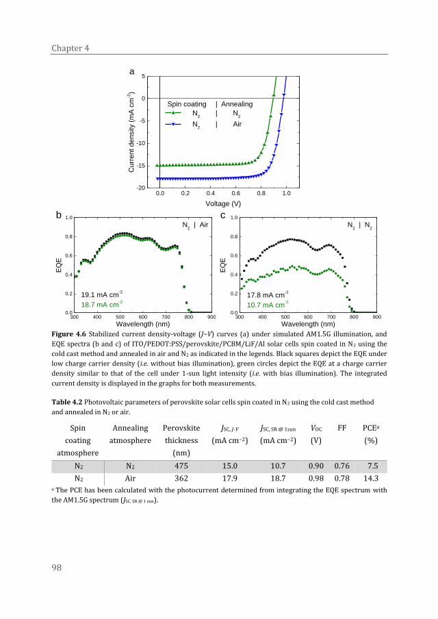
Chapter 4
98
0.0 0.2 0.4 0.6 0.8 1.0-20
-15
-10
-5
0
5
Cu
rre
nt
de
nsity (
mA
cm
-2)
Voltage (V)
Spin coating | Annealing
N2 | N
2
N2 | Air
a
300 400 500 600 700 800 9000.0
0.2
0.4
0.6
0.8
1.0
19.1 mA cm-2
18.7 mA cm-2
N2 | Air
EQ
E
Wavelength (nm)
b
300 400 500 600 700 800 9000.0
0.2
0.4
0.6
0.8
1.0
17.8 mA cm-2
10.7 mA cm-2
EQ
E
Wavelength (nm)
N2 | N
2
c
Figure 4.6 Stabilized current density-voltage (J−V) curves (a) under simulated AM1.5G illumination, and
EQE spectra (b and c) of ITO/PEDOT:PSS/perovskite/PCBM/LiF/Al solar cells spin coated in N2 using the
cold cast method and annealed in air and N2 as indicated in the legends. Black squares depict the EQE under
low charge carrier density (i.e. without bias illumination), green circles depict the EQE at a charge carrier
density similar to that of the cell under 1-sun light intensity (i.e. with bias illumination). The integrated
current density is displayed in the graphs for both measurements.
Table 4.2 Photovoltaic parameters of perovskite solar cells spin coated in N2 using the cold cast method
and annealed in N2 or air.
Spin
coating
atmosphere
Annealing
atmosphere
Perovskite
thickness
(nm)
JSC, J-V
(mA cm−2)
JSC, SR @ 1sun
(mA cm−2)
VOC
(V)
FF PCEa
(%)
N2 N2 475 15.0 10.7 0.90 0.76 7.5
N2 Air 362 17.9 18.7 0.98 0.78 14.3 a The PCE has been calculated with the photocurrent determined from integrating the EQE spectrum with
the AM1.5G spectrum (JSC, SR @ 1 sun).
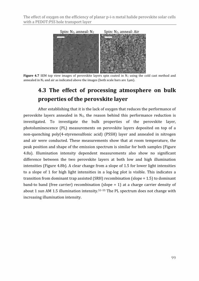
The effect of oxygen on the efficiency of planar p-i-n metal halide perovskite solar cells with a PEDOT:PSS hole transport layer
99
Spin: N2, anneal: N2 Spin: N2, anneal: Air
Figure 4.7 SEM top view images of perovskite layers spin coated in N2 using the cold cast method and
annealed in N2 and air as indicated above the images (both scale bars are 1µm).
4.3 The effect of processing atmosphere on bulk
properties of the perovskite layer
After establishing that it is the lack of oxygen that reduces the performance of
perovskite layers annealed in N2, the reason behind this performance reduction is
investigated. To investigate the bulk properties of the perovskite layer,
photoluminescence (PL) measurements on perovskite layers deposited on top of a
non-quenching poly(4-styrenesulfonic acid) (PSSH) layer and annealed in nitrogen
and air were conducted. These measurements show that at room temperature, the
peak position and shape of the emission spectrum is similar for both samples (Figure
4.8a). Illumination intensity dependent measurements also show no significant
difference between the two perovskite layers at both low and high illumination
intensities (Figure 4.8b). A clear change from a slope of 1.5 for lower light intensities
to a slope of 1 for high light intensities in a log-log plot is visible. This indicates a
transition from dominant trap assisted (SRH) recombination (slope = 1.5) to dominant
band-to band (free carrier) recombination (slope = 1) at a charge carrier density of
about 1 sun AM 1.5 illumination intensity.52–55 The PL spectrum does not change with
increasing illumination intensity.
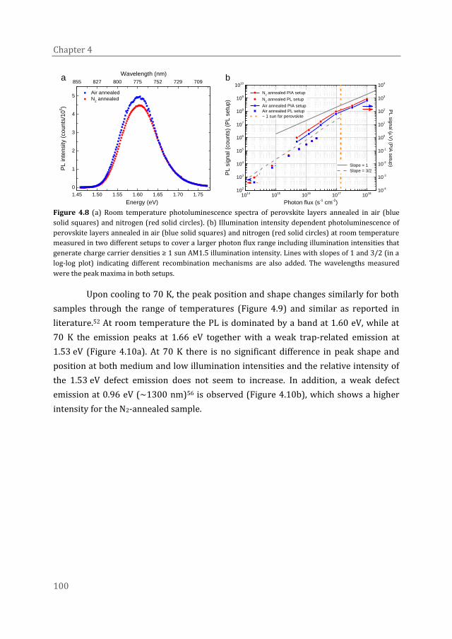
Chapter 4
100
1.45 1.50 1.55 1.60 1.65 1.70 1.75
855 827 800 775 752 729 709
0
1
2
3
4
5
Wavelength (nm)
PL inte
nsity (
counts
/10
5)
Energy (eV)
Air annealed
N2 annealed
a
102
103
104
105
106
107
108
109
1010
1014
1015
1016
1017
1018
10-4
10-3
10-2
10-1
100
101
102
103
104
Slope = 1
Slope = 3/2
Photon flux (s-1 cm
-2)
PL
sig
na
l (c
ou
nts
) (P
L s
etu
p)
N2 annealed PIA setup
N2 annealed PL setup
Air annealed PIA setup
Air annealed PL setup
~ 1 sun for perovskite
PL s
ignal (
V) (P
IA s
etu
p)
b
Figure 4.8 (a) Room temperature photoluminescence spectra of perovskite layers annealed in air (blue
solid squares) and nitrogen (red solid circles). (b) Illumination intensity dependent photoluminescence of
perovskite layers annealed in air (blue solid squares) and nitrogen (red solid circles) at room temperature
measured in two different setups to cover a larger photon flux range including illumination intensities that
generate charge carrier densities ≥ 1 sun AM1.5 illumination intensity. Lines with slopes of 1 and 3/2 (in a
log-log plot) indicating different recombination mechanisms are also added. The wavelengths measured
were the peak maxima in both setups.
Upon cooling to 70 K, the peak position and shape changes similarly for both
samples through the range of temperatures (Figure 4.9) and similar as reported in
literature.52 At room temperature the PL is dominated by a band at 1.60 eV, while at
70 K the emission peaks at 1.66 eV together with a weak trap-related emission at
1.53 eV (Figure 4.10a). At 70 K there is no significant difference in peak shape and
position at both medium and low illumination intensities and the relative intensity of
the 1.53 eV defect emission does not seem to increase. In addition, a weak defect
emission at 0.96 eV (~1300 nm)56 is observed (Figure 4.10b), which shows a higher
intensity for the N2-annealed sample.

The effect of oxygen on the efficiency of planar p-i-n metal halide perovskite solar cells with a PEDOT:PSS hole transport layer
101
1.5 1.6 1.7
0.0
0.5
1.00.0
0.5
1.00.0
0.5
1.00.0
0.5
1.00.0
0.5
1.00.0
0.5
1.0
827 775 729
0.0
0.5
1.0
Energy (eV)
70 K
100 K
120 K
Norm
aliz
ed P
L inte
nsity
150 K
200 K
250 K
N2
Air
Wavelength (nm)
295 K
Figure 4.9 Normalized photoluminescence spectra of perovskite layers annealed in nitrogen (red) and air
(blue) through a range of temperatures while cooling down from room temperature to 70 K.
1.45 1.50 1.55 1.60 1.65 1.70 1.7510
0
101
102
103
104
105
106
PL-inte
nsity (
co
un
ts)
Energy (eV)
N2-annealed
Air-annealed
a
0.90 0.95 1.00 1.05
3
3.5
4
4.5
5
PL inte
nsity (
co
un
ts/1
04)
Energy (eV)
Air annealed
N2 annealed
Dark count value
b
Figure 4.10 Photoluminescence spectra at 70 K of perovskite layers annealed in air (blue) and nitrogen
(red) at high (dashed lines) and low (solid lines) illumination intensities.
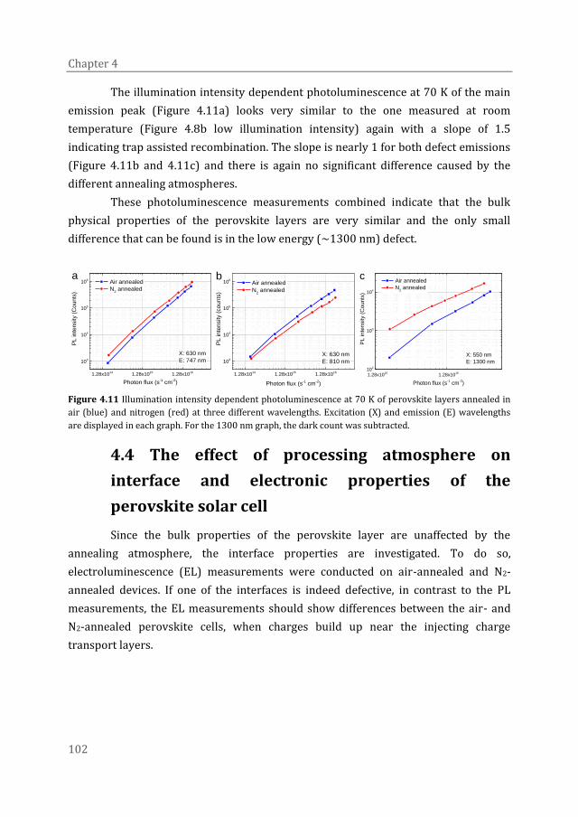
Chapter 4
102
The illumination intensity dependent photoluminescence at 70 K of the main
emission peak (Figure 4.11a) looks very similar to the one measured at room
temperature (Figure 4.8b low illumination intensity) again with a slope of 1.5
indicating trap assisted recombination. The slope is nearly 1 for both defect emissions
(Figure 4.11b and 4.11c) and there is again no significant difference caused by the
different annealing atmospheres.
These photoluminescence measurements combined indicate that the bulk
physical properties of the perovskite layers are very similar and the only small
difference that can be found is in the low energy (~1300 nm) defect.
1.28x10¹⁴
1.28x10¹⁵
1.28x10¹⁶
103
104
105
106
X: 630 nm
E: 747 nm
PL
in
ten
sity (
Co
un
ts)
Photon flux (s-1 cm
-2)
Air annealed
N2 annealed
a
1.28x10¹⁴
1.28x10¹⁵
1.28x10¹⁶
103
104
105
106
X: 630 nm
E: 810 nm
PL inte
nsity (
co
un
ts)
Photon flux (s-1 cm
-2)
Air annealed
N2 annealed
b
1.28x10¹⁵
1.28x10¹⁶
102
103
104
X: 550 nm
E: 1300 nmP
L inte
nsity (
Co
un
ts)
Photon flux (s-1 cm
-2)
Air annealed
N2 annealed
c
Figure 4.11 Illumination intensity dependent photoluminescence at 70 K of perovskite layers annealed in
air (blue) and nitrogen (red) at three different wavelengths. Excitation (X) and emission (E) wavelengths
are displayed in each graph. For the 1300 nm graph, the dark count was subtracted.
4.4 The effect of processing atmosphere on
interface and electronic properties of the
perovskite solar cell
Since the bulk properties of the perovskite layer are unaffected by the
annealing atmosphere, the interface properties are investigated. To do so,
electroluminescence (EL) measurements were conducted on air-annealed and N2-
annealed devices. If one of the interfaces is indeed defective, in contrast to the PL
measurements, the EL measurements should show differences between the air- and
N2-annealed perovskite cells, when charges build up near the injecting charge
transport layers.
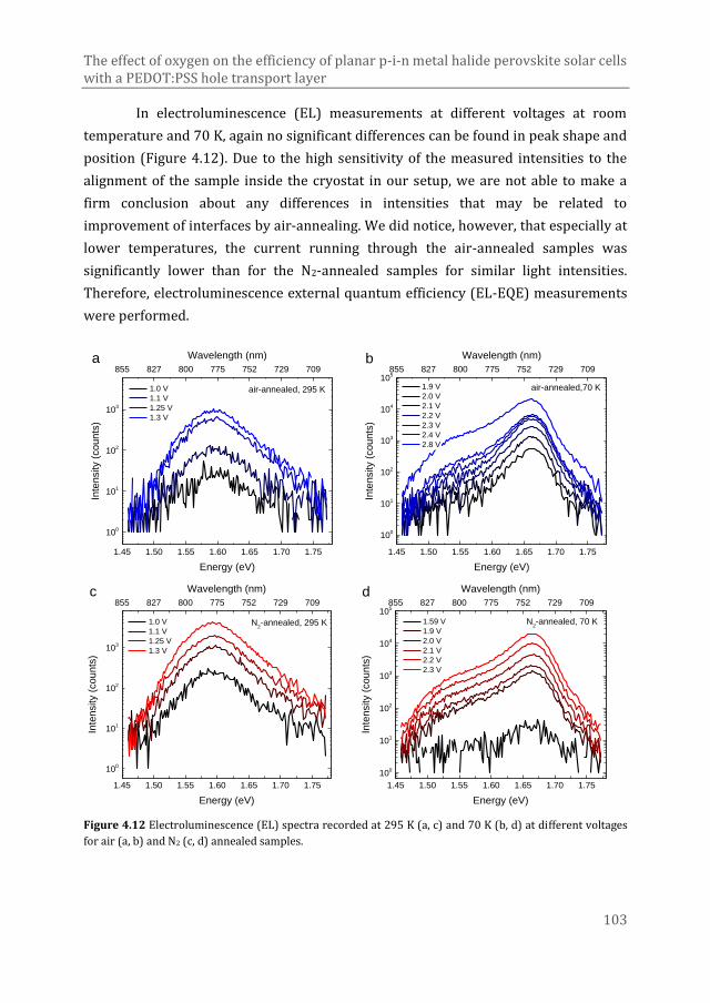
The effect of oxygen on the efficiency of planar p-i-n metal halide perovskite solar cells with a PEDOT:PSS hole transport layer
103
In electroluminescence (EL) measurements at different voltages at room
temperature and 70 K, again no significant differences can be found in peak shape and
position (Figure 4.12). Due to the high sensitivity of the measured intensities to the
alignment of the sample inside the cryostat in our setup, we are not able to make a
firm conclusion about any differences in intensities that may be related to
improvement of interfaces by air-annealing. We did notice, however, that especially at
lower temperatures, the current running through the air-annealed samples was
significantly lower than for the N2-annealed samples for similar light intensities.
Therefore, electroluminescence external quantum efficiency (EL-EQE) measurements
were performed.
1.45 1.50 1.55 1.60 1.65 1.70 1.75
855 827 800 775 752 729 709
100
101
102
103
Wavelength (nm)
Inte
nsity (
coun
ts)
Energy (eV)
1.0 V
1.1 V
1.25 V
1.3 V
air-annealed, 295 K
a
1.45 1.50 1.55 1.60 1.65 1.70 1.75
855 827 800 775 752 729 709
100
101
102
103
104
105
Wavelength (nm)
Inte
nsity (
coun
ts)
Energy (eV)
1.9 V
2.0 V
2.1 V
2.2 V
2.3 V
2.4 V
2.8 V
air-annealed,70 K
b
1.45 1.50 1.55 1.60 1.65 1.70 1.75
855 827 800 775 752 729 709
100
101
102
103
Wavelength (nm)
Inte
nsity (
coun
ts)
Energy (eV)
1.0 V
1.1 V
1.25 V
1.3 V
N2-annealed, 295 K
c
1.45 1.50 1.55 1.60 1.65 1.70 1.75
855 827 800 775 752 729 709
100
101
102
103
104
105
Wavelength (nm)
Inte
nsity (
coun
ts)
Energy (eV)
1.59 V
1.9 V
2.0 V
2.1 V
2.2 V
2.3 V
N2-annealed, 70 K
d
Figure 4.12 Electroluminescence (EL) spectra recorded at 295 K (a, c) and 70 K (b, d) at different voltages
for air (a, b) and N2 (c, d) annealed samples.

Chapter 4
104
These EL-EQE measurements at room temperature show that the EL-EQE of
perovskite layers annealed in air is higher than that of perovskite layers annealed in
nitrogen (Figure 4.13a), which holds up to high current densities (>100 mA cm−2). It
can be seen that the current-voltage characteristics are similar (except for the ~0.1 V
shifted onset, see Figure 4.13b) and that between 1.0 and 1.3 V, the light emitted by
the air-annealed device is higher than for the N2-annealed device. Because the current
through the perovskite cells is similar for both annealing atmospheres (Fig 4.12b), this
indicates that the air-annealed cells show electroluminescence at lower voltages,
consistent with less traps that need to be filled before charges can recombine
radiatively.
Combining the room- and low-temperature PL and the room temperature EL
and VOC vs light intensity results, we conclude that the improvement of the solar cell
performance in the air-annealed perovskite layers is not primarily due to a change in
the bulk properties of the perovskite layer but rather due to an improvement of the
PEDOT:PSS / perovskite interface.
0 20 40 60 80 1000.0
0.5
1.0
1.5
2.0
2.5a
EL-E
QE
(x 1
0-7)
Current density (mA cm-2)
N2 annealed
Air annealed
0.5 0.7 0.9 1.1 1.3
0
5
10 N
2-annealed
Air-anneled
Voltage (V)
Cu
rrent te
stc
ell
(mA
)
0
1
2
3
Cu
rrent S
i ph
oto
dio
de
(nA
)
b
Figure 4.13 (a) EL-EQE measurements of solar cells with perovskite layers annealed in air (blue solid
squares) and N2 (red solid circles). (b) Current-voltage characteristics of the perovskite devices (solid
symbols) and the simultaneously recorded photocurrent of a silicon photodiode placed on top during the
EL-EQE measurements

The effect of oxygen on the efficiency of planar p-i-n metal halide perovskite solar cells with a PEDOT:PSS hole transport layer
105
4.5 The effect of processing atmosphere on the
PEDOT:PSS / perovskite interface
We have shown that oxygen exposure during annealing is required for
producing high performance solar cells and that likely the PEDOT:PSS/perovskite
interface deteriorates when the perovskite layer is annealed in N2. It has been
reported that PEDOT:PSS can be reduced (electro)chemically by the application of a
voltage57 or by exposure to polyethylenimine (PEI)58 and methylamine (MA)59 vapor.
In the latter case, the reduced PEDOT:PSS can be re-oxidized by exposure to oxygen.59
To investigate this effect in more detail, PEDOT:PSS layers were spin coated onto glass
slides and perovskite layers were hot cast onto the PEDOT:PSS layers in a N2
atmosphere both using the same processing parameters as used for solar cell
fabrication. The perovskite layers were then annealed, either in ambient air or in N2
and subsequently the perovskite layers were washed off from the underlying
PEDOT:PSS layers using pure DMF. The resulting PEDOT:PSS layers were analyzed
and compared to fresh PEDOT:PSS layers using UV-vis-NIR spectroscopy (Figure
4.14). The spectra show that the polaron absorption at 900 nm of the PEDOT:PSS layer
that was underneath the N2-annealed perovskite layer, is higher than that of fresh
PEDOT:PSS, and that the bipolaron band at wavelengths ≥ 1100 nm is lower in
intensity (Figure 4.14a). These are two clear signatures of chemical de-doping of
PEDOT.59 In contrast, the UV-vis-NIR spectrum of the PEDOT:PSS layer that was
underneath the air-annealed perovskite layer is very similar to the spectrum of the
fresh PEDOT:PSS layer, apart from a narrow peak at 400 nm. The onset and peak
position of the 400 nm absorption coincides with the absorbance of orthorhombic
lead oxide (PbO)60 and tri-iodide (I3−),61 both of which could be present in the
PEDOT:PSS film after deposition and washing off the perovskite layer. The presence of
either of the two could however not be confirmed by XPS measurements.
To confirm that the de-doping of the PEDOT:PSS layer is reversible, the
PEDOT:PSS layer that was underneath the N2-annealed perovskite layer was exposed
to air (Figure 4.14b). Air exposure of the de-doped PEDOT:PSS layer up to 180
minutes does indeed re-oxidize the PEDOT, evidenced by a reduced polaron
absorption at 900 nm and an increased bipolaron absorption above 1100 nm.
Annealing of the reduced PEDOT:PSS layer in air speeds up the re-oxidation reaction
and prolonged air exposure almost completely re-oxidizes the PEDOT.

Chapter 4
106
400 600 800 1000 1200 1400 1600 18000.04
0.05
0.06
0.07
0.08
0.09
0.10
0.11
0.12
Absorb
ance (
O.D
.)
Wavelength (nm)
PEDOT
N2 annealed
Air annealed
a
400 600 800 1000 1200 1400 1600 18000.06
0.07
0.08
0.09
0.10
0.11
0.12
Subsequent anneal (min)
10
30
30 + overnight air exp.
30 + 3 day air exp.
Absorb
ance (
O.D
.)
Wavelength (nm)
Air exposure time (min)
0
30
60
90
100
150
180
b
Figure 4.14 (a) UV-vis-NIR spectra of a fresh PEDOT:PSS layer and PEDOT:PSS layers on which perovskite
layers were deposited, annealed and washed off again. (b) UV-vis-NIR spectra of the PEDOT:PSS layer that
was underneath the N2-annealed perovskite layer upon air exposure vs time.
Ultraviolet photoelectron spectroscopy (UPS) measurements were performed
on air- and N2-annealed perovskite layers and on the PEDOT:PSS layers that were
underneath, after washing off the perovskite, to investigate the effect of the reduction
and re-oxidation of the PEDOT:PSS layer on the electronic properties of the materials
(Figure 4.15 and Table 4.3). By comparing to UPS results for PEDOT:PSS, and
PEDOT:PSS that was treated with DMF (Table 4.3), we see that just casting hot DMF on
top of PEDOT:PSS already reduces both the work function (WF, Fermi energy) and
ionization potential (IP, valence band energy) of a PEDOT:PSS layer. By subsequent
washing with DMF at room temperature, a further decrease can be seen. The striking
result is that with spin coating the perovskite precursor on PEDOT:PSS, annealing and
washing off of the perovskite layer from the PEDOT:PSS layer, the WF is equal to the
IP. The other important observation is that the WF and IP of the PEDOT:PSS layer that
was underneath a N2-annealed perovskite film is lower compared to the PEDOT:PSS
layer that was underneath an air-annealed perovskite layer. Looking at the results of
the perovskite layers deposited on PEDOT:PSS, we see a similar difference with the N2
annealed perovskite layer showing a lower WF than the air annealed one, while the IP
of the two perovskite layers remains equal. This suggests that the WF of the
perovskite layer is influenced by that of the PEDOT:PSS beneath it. It is worth to note
that the difference between the WF of the PEDOT:PSS layer and that of the perovskite
layer is similar (~0.5 eV) for both annealing atmospheres. The difference in the value
of the WF of the perovskite layers results in a difference in the built-in voltage of the
solar cells, allowing the VOC of the air-annealed perovskite layer to exceed that of the
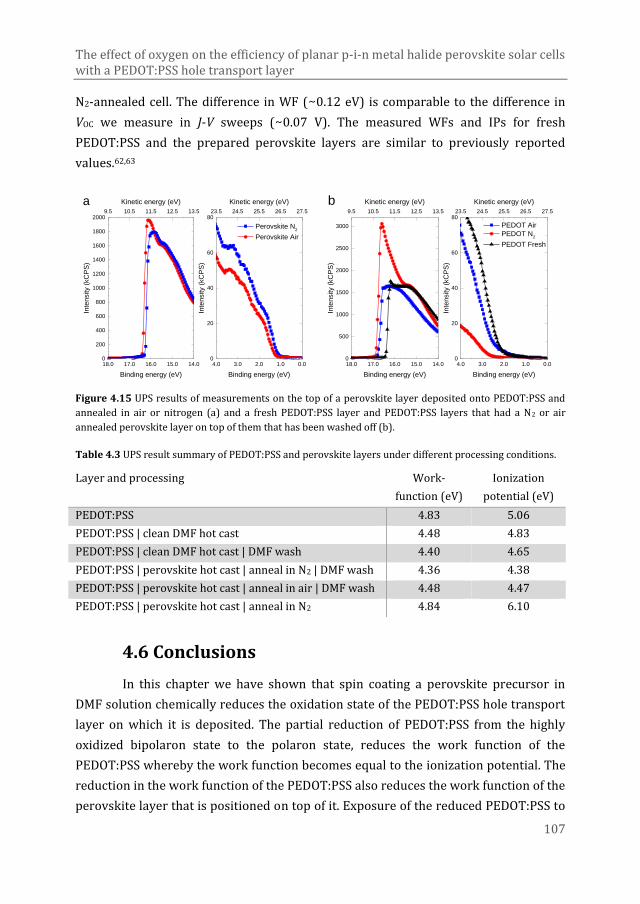
The effect of oxygen on the efficiency of planar p-i-n metal halide perovskite solar cells with a PEDOT:PSS hole transport layer
107
N2-annealed cell. The difference in WF (~0.12 eV) is comparable to the difference in
VOC we measure in J-V sweeps (~0.07 V). The measured WFs and IPs for fresh
PEDOT:PSS and the prepared perovskite layers are similar to previously reported
values.62,63
18.0 17.0 16.0 15.0 14.0
9.5 10.5 11.5 12.5 13.5
0
200
400
600
800
1000
1200
1400
1600
1800
2000
Kinetic energy (eV)
Inte
nsity (
kC
PS
)
Binding energy (eV)
4.0 3.0 2.0 1.0 0.0
23.5 24.5 25.5 26.5 27.5
0
20
40
60
80
Perovskite N2
Perovskite Air
Kinetic energy (eV)In
tensity (
kC
PS
)
Binding energy (eV)
a
18.0 17.0 16.0 15.0 14.0
9.5 10.5 11.5 12.5 13.5
0
500
1000
1500
2000
2500
3000
Kinetic energy (eV)
Inte
nsity (
kC
PS
)
Binding energy (eV)
b
4.0 3.0 2.0 1.0 0.0
23.5 24.5 25.5 26.5 27.5
0
20
40
60
80
PEDOT Air
PEDOT N2
PEDOT Fresh
Kinetic energy (eV)
Inte
nsity (
kC
PS
)
Binding energy (eV)
Figure 4.15 UPS results of measurements on the top of a perovskite layer deposited onto PEDOT:PSS and
annealed in air or nitrogen (a) and a fresh PEDOT:PSS layer and PEDOT:PSS layers that had a N2 or air
annealed perovskite layer on top of them that has been washed off (b).
Table 4.3 UPS result summary of PEDOT:PSS and perovskite layers under different processing conditions.
Layer and processing Work-
function (eV)
Ionization
potential (eV)
PEDOT:PSS 4.83 5.06
PEDOT:PSS | clean DMF hot cast 4.48 4.83
PEDOT:PSS | clean DMF hot cast | DMF wash 4.40 4.65
PEDOT:PSS | perovskite hot cast | anneal in N2 | DMF wash 4.36 4.38
PEDOT:PSS | perovskite hot cast | anneal in air | DMF wash 4.48 4.47
PEDOT:PSS | perovskite hot cast | anneal in N2 4.84 6.10
4.6 Conclusions
In this chapter we have shown that spin coating a perovskite precursor in
DMF solution chemically reduces the oxidation state of the PEDOT:PSS hole transport
layer on which it is deposited. The partial reduction of PEDOT:PSS from the highly
oxidized bipolaron state to the polaron state, reduces the work function of the
PEDOT:PSS whereby the work function becomes equal to the ionization potential. The
reduction in the work function of the PEDOT:PSS also reduces the work function of the
perovskite layer that is positioned on top of it. Exposure of the reduced PEDOT:PSS to
Chapter 4
108
oxygen re-oxidizes the PEDOT:PSS. Even relatively short exposure (8 minutes) of the
PEDOT:PSS layer during the annealing of the perovskite layer that is on top of it
(partially) restores the oxidation state of the PEDOT and restores its functionality in
the solar cell. The bulk properties of the perovskite layer do not seem to change by
annealing in different atmospheres. Annealing the perovskite layers in an inert
atmosphere therefore produces solar cells of inferior performance, displaying lower
VOC and a JSC that is sublinear with light intensity compared to air-annealed devices.
4.7 Experimental
Device fabrication
Indium-tin oxide (ITO) coated and pre-patterned glass substrates (Naranjo
substrates) were cleaned by sonication in acetone (Sigma Aldrich), scrubbing in a
solution of sodium dodecyl sulfate (SDS, Acros, 99%) in filtered water (Milli-Q),
rinsing in deionized water, sonication in 2-propanol (Sigma Aldrich) and 30 minutes
of UV-ozone treatment right before use. Poly(3,4-ethylenedioxythiophene):
polystyrene sulfonate (PEDOT:PSS, Heraeus Clevios PVP Al 4083) was filtered using a
0.45 µm PVDF filter and spin coated (60 s, 3000 RPM) onto the cleaned substrates.
For the hot casting method, the PEDOT:PSS coated substrate was heated for 1
minute at 100 °C right before use, for the cold casting method, the PEDOT:PSS coated
substrates were dried at 140 °C for 15 minutes. For the electron transport layer, PCBM
(Solenne BV, 99%) was dissolved in a 1:1 (v/v) mixture of chloroform (Biosolve, AR
grade) and chlorobenzene (Sigma Aldrich, anhydrous 99.8%) at 20 mg mL−1. The
perovskite precursor solution for use with the hot casting method was prepared by
weighing 476.9 mg of methylammonium iodide (Dyesol), 303.5 mg of lead(II) acetate
trihydrate (Sigma Aldrich, 99.999% trace metal basis) and 55.6 mg of lead(II) chloride
(Sigma Aldrich, 98%) in air and adding 1 mL of N,N-dimethylformamide (Sigma
Aldrich, anhydrous, 99.8%). The mixture was stirred for 30 minutes at room
temperature to completely dissolve all compounds and stirred at 70 °C for 30 minutes
before use. The solution was then spin coated onto pre-heated (100 °C) PEDOT:PSS-
covered substrates (60 µL, 20 s, 5700 RPM, dynamic) using a specially designed spin
coating chuck that minimizes contact between the substrate and the chuck to avoid
rapid cooling of the substrate. The perovskite layer was then annealed immediately
(100 °C, 8 minutes) and after 1 minute of cooling, coated with PCBM (Solenne BV,
99%) (30 s, 1000 RPM). The device was then transferred into a glovebox, the contact

The effect of oxygen on the efficiency of planar p-i-n metal halide perovskite solar cells with a PEDOT:PSS hole transport layer
109
area was cleaned and LiF (1 nm) and Al (100 nm) were thermally evaporated under
high vacuum (±3 × 10⁻⁷ mbar) as a back electrode.
The perovskite precursor solution for use with the cold casting method was
made by weighing 858.4 mg of methylammonium iodide (Dyesol), 546.3 mg of lead(II)
acetate trihydrate (Sigma Aldrich, 99.999% trace metal basis) and 100.1 mg of lead(II)
chloride (Sigma Aldrich, 98%) and adding 1 mL of N,N-dimethylformamide (Sigma
Aldrich, anhydrous, 99.8%). The mixture was stirred for 30 minutes at room
temperature to completely dissolve all the compounds. The solution was then spin
coated onto the cleaned, PEDOT:PSS-coated and dried substrates (60 µL, 120 s, 5700
RPM) using the same specially designed spin coating chuck. The perovskite layer was
then annealed immediately (100 °C, 15 minutes) and coated with PCBM (Solenne BV,
99%) (30 s, 500 RPM). The device contact area was cleaned and LiF (1 nm) and Al
(100 nm) were thermally evaporated under high vacuum (±3 × 10⁻⁷ mbar) as a back
electrode.
To accurately control the temperature of the hotplate surfaces of different
hotplates, aluminum slabs were used to achieve a homogeneous surface temperature
and a surface temperature probe (Testo 0560 1109 mini surface thermometer) was
used to measure the temperature. The mentioned temperatures are the temperatures
set on the hotplate thermocouple. A set temperature of 100 °C corresponds to a
temperature of 94 °C at the top of the aluminum slab measured with the surface
probe.
Measurement methods
Layer thicknesses were measured using a Veeco Dektak 150 profilometer.
J–V characteristics were measured in a nitrogen environment with a Keithley
2400 source meter under ±100 mW cm−2 white light illumination from a tungsten-
halogen lamp filtered by a Schott GG385 UV filter and a Hoya LB120 daylight filter.
The cells were masked with a 0.0676 cm2 or 0.1296 cm2 aperture (the physical
overlap of the contacts is 0.09 cm2 and 0.16 cm2 respectively). The stabilized J-V
measurement protocol used was defined by light soaking at VOC for 5 minutes,
followed by a downward sweep (VOC + 0.04 V → −0.04 V) with a step size of 0.02 V. At
each voltage the current density was recorded for 10 s and the final value was used for
plotting the J−V curve. Fast upwards and downwards J–V sweeps were performed
before and after the slow sweep measurement between −0.5 and 1.5 V with a scan
speed of 0.25 V s−1.
Short-circuit current densities under AM 1.5G conditions were determined by
integrating the spectral response with the solar spectrum. Spectral response
Chapter 4
110
measurements were conducted under only probe light and 1-sun equivalent operating
conditions by using a 530 nm high power LED (Thorlabs M530L3 driven by a DC4104
driver) for bias illumination. The device was kept in a nitrogen filled box behind a
quartz window and a circular aperture with a 1 mm radius and irradiated with
modulated monochromatic light, from a 50 W tungsten-halogen lamp (Philips
focusline) and monochromator (Oriel, Cornerstone 130) with the use of a mechanical
chopper (160 Hz). The response was recorded as a voltage from a preamplifier
(SR570) using a lock-in amplifier (SR830). A calibrated silicon cell was used as
reference (calibrated at the Energy Research Centre of the Netherlands).
JSC and VOC vs light intensity measurements were performed using a Keithley
2400 source meter and 405 and 730 nm high power LEDs (Thorlabs M405L3 and
M730L4 driven by a DC4104 driver) for illumination.
Scanning electron microscopy (SEM) was performed on a FEI Quanta 3D FEG.
X‐Ray Diffraction measurements were performed on a Bruker 2D Phaser
using Cu Kα radiation with a wavelength of 0.15406 nm between 2θ angles of 10 to
60° using increments of 0.05° and a 2 second integration time. A 0.6 mm slit was used
at the X‐Ray source and a shield was positioned 0.5 mm above the sample surface. The
sample rotated at a speed of 60 RPM during the measurement.
Low intensity photoluminescence measurements were performed using an
Edinburgh Instruments FLSP920 double-monochromator luminescence spectrometer
equipped with a multialkali photomultiplier tube and a nitrogen-cooled near IR
sensitive photomultiplier (Hamamatsu). The substrate was positioned inside an
Oxford Optistat cryostat under a dynamic vacuum. Cryogenic temperatures were
achieved by indirectly cooling the substrate. The photoluminescence spectrometer has
an internal uncalibrated photodetector to monitor the intensity of excitation beam of
which the output is in counts per second. We have used a calibrated Si solar cell to
calibrate the reference detector. The light from a Xenon light source is
monochromated to specific wavelengths for the PL measurements.
High intensity photoluminescence measurements were performed using a
532 nm laser (B&W tek inc. BWN-532-20E/56486) excitation that was chopped using
a mechanical chopper (277 Hz). The sample was located in an Oxford Optistat cryostat
under dynamic vacuum. The signal was measured using a monochromator (Oriel
77700 at 775 nm) and a Si diode linked to a lock-in amplifier (SR830DSP). The
illumination intensity was varied using a double optical density filter wheel (New
Focus 5215) and was calibrated at different OD settings using a Si photodiode. The
The effect of oxygen on the efficiency of planar p-i-n metal halide perovskite solar cells with a PEDOT:PSS hole transport layer
111
illumination area of the laser beam was determined at different optical densities using
a Gentec Beamage 3.0 beam diagnostic tool (1/e2 value was used).
Electroluminescence measurements were performed in a nitrogen
environment using a reference Si cell and two Keithley 2400 source meters to control
the voltage and record the current flowing through the test cell and record the current
flow out of the Si reference cell. Dividing the two current flows results in a crude
electroluminescence external quantum efficiency value that is not absolute but can be
used to compare samples measured in the same setup.
UPS measurements were performed in a multi-chamber ESCALAB II system
using 6 V bias and the HeI line at 21.22 eV. The Fermi level reference was established
on an in situ sputter-cleaned Au film. The ionization potential and the work function
are derived from the energy difference between the secondary electron edge and,
respectively, the valence band edge or the position of the Fermi energy. Samples were
transferred from gloveboxes to the measurement equipment completely in an N2
atmosphere to avoid any effects of oxygen exposure.
4.8 References
1 A. Kojima, K. Teshima, Y. Shirai and T. Miyasaka, J. Am. Chem. Soc., 2009, 131, 6050–
6051.
2 H.-S. Kim, C.-R. Lee, J.-H. Im, K.-B. Lee, T. Moehl, A. Marchioro, S.-J. Moon, R. Humphry-
Baker, J.-H. Yum, J. E. Moser, M. Grätzel and N.-G. Park, Sci. Rep., 2012, 2, 591.
3 M. M. Lee, J. Teuscher, T. Miyasaka, T. N. Murakami and H. J. Snaith, Science, 2012, 338,
643–648.
4 M. Saliba, T. Matsui, J.-Y. Seo, K. Domanski, J.-P. Correa-Baena, M. K. Nazeeruddin, S. M.
Zakeeruddin, W. Tress, A. Abate, A. Hagfeldt and M. Grätzel, Energy Environ. Sci., 2016,
9, 1989–1997.
5 W. S. Yang, B.-W. Park, E. H. Jung, N. J. Jeon, Y. C. Kim, D. U. Lee, S. S. Shin, J. Seo, E. K.
Kim, J. H. Noh and S. Il Seok, Science., 2017, 356, 1376–1379.
6 V. D’Innocenzo, G. Grancini, M. J. P. Alcocer, A. R. S. Kandada, S. D. Stranks, M. M. Lee, G.
Lanzani, H. J. Snaith and A. Petrozza, Nat. Commun., 2014, 5, 3586.
7 L. M. Pazos-Outón, M. Szumilo, R. Lamboll, J. M. Richter, M. Crespo-Quesada, M. Abdi-
Jalebi, H. J. Beeson, M. Vrućinić, M. Alsari, H. J. Snaith, B. Ehrler, R. H. Friend and F.
Deschler1, Science., 2016, 351, 1430-1433.
8 C.-S. Jiang, M. Yang, Y. Zhou, B. To, S. U. Nanayakkara, J. M. Luther, W. Zhou, J. J. Berry, J.
Van De Lagemaat, N. P. Padture, K. Zhu and M. M. Al-jassim, Nat. Commun., 2015, 6,
8397.
Chapter 4
112
9 C. Wehrenfennig, G. E. Eperon, M. B. Johnston, H. J. Snaith and L. M. Herz, Adv. Mater.,
2014, 26, 1584–1589.
10 T. M. Schmidt, T. T. Larsen-Olsen, J. E. Carlé, D. Angmo and F. C. Krebs, Adv. Energy
Mater., 2015, 5, 1500569
11 K. Hwang, Y.-S. Jung, Y.-J. Heo, F. H. Scholes, S. E. Watkins, J. Subbiah, D. J. Jones, D.-Y.
Kim and D. Vak, Adv. Mater., 2015, 27, 1241–1247.
12 Y. Galagan, E. W. C. Coenen, W. J. H. Verhees and R. Andriessen, J. Mater. Chem. A, 2016,
4, 5700–5705.
13 G. E. Eperon, S. D. Stranks, C. Menelaou, M. B. Johnston, L. M. Herz and H. J. Snaith,
Energy Environ. Sci., 2014, 7, 982-988.
14 G. E. Eperon, G. M. Paternò, R. J. Sutton, A. Zampetti, A. A. Haghighirad, F. Cacialli and H.
J. Snaith, J. Mater. Chem. A., 2015, 3, 19688–19695.
15 W. Liao, D. Zhao, Y. Yu, N. Shrestha, K. Ghimire, C. R. Grice, C. Wang, Y. Xiao, A. J.
Cimaroli, R. J. Ellingson, N. J. Podraza, K. Zhu, R. G. Xiong and Y. Yan, J. Am. Chem. Soc.,
2016, 138, 12360–12363.
16 J. H. Heo, D. H. Song, H. J. Han, S. Y. Kim, J. H. Kim, D. Kim, H. W. Shin, T. K. Ahn, C. Wolf,
T. W. Lee and S. H. Im, Adv. Mater., 2015, 27, 3424–3430.
17 C.-C. Chueh, C.-Y Liao, F. Zuo, S. T. Williams, P.-W. Liang and A. K.-Y. Jen, J. Mater. Chem.
A, 2015, 3, 9058–9062.
18 W. Zhang, M. Saliba, D. T. Moore, S. K. Pathak, M. T. Hörantner, T. Stergiopoulos, S. D.
Stranks, G. E. Eperon, J. A. Alexander-Webber, A. Abate, A. Sadhanala, S. Yao, Y. Chen, R.
H. Friend, L. A. Estroff, U. Wiesner and H. J. Snaith, Nat Commun, 2015, 6, 6142.
19 K. L. Gardner, J. G. Tait, T. Merckx, W. Qiu, U. W. Paetzold, L. Kootstra, M. Jaysankar, R.
Gehlhaar, D. Cheyns, P. Heremans and J. Poortmans, Adv. Energy Mater., 2016, 6,
1600386.
20 K. H. Hendriks, J. J. van Franeker, B. J. Bruijnaers, J. A. Anta, M. M. Wienk and R. A. J.
Janssen, J. Mater. Chem. A., 2017, 5, 2346.
21 S. Bae, S. J. Han, T. J. Shin and W. H. Jo, J. Mater. Chem. A, 2015, 3, 23964–23972.
22 N. Ahn, D.-Y. Son, I.-H. Jang, S. M. Kang, M. Choi and N.-G. Park, J. Am. Chem. Soc., 2015,
137, 8696–8699.
23 N. K. Noel, S. N. Habisreutinger, B. Wenger, M. T. Klug, M. T. Hörantner, M. B. Johnston,
R. J. Nicholas, D. T. Moore and H. J. Snaith, Energy Environ. Sci., 2017, 10, 145-152.
24 F. K. Aldibaja, L. Badia, E. Mas-Marzá, R. S. Sánchez, E. M. Barea and I. Mora-Sero, J.
Mater. Chem. A, 2015, 3, 9194–9200.
25 G. Li, T. Zhang and Y. Zhao, J. Mater. Chem. A., 2015, 3, 19674–19678.
26 W. Qiu, T. Merckx, M. Jaysankar, C. Masse de la Huerta, L. Rakocevic, W. Zhang, U. W.
Paetzold, R. Gehlhaar, L. Froyen, J. Poortmans, D. Cheyns, H. J. Snaith and P. Heremans,
Energy Environ. Sci., 2016, 9, 484-489.
27 J. Qing, H.-T. Chandran, Y.-H. Cheng, X.-K. Liu, H.-W. Li, S.-W. Tsang, M.-F. Lo and C.-S.
Lee, ACS Appl. Mater. Interfaces, 2015, 7, 23110–23116.
The effect of oxygen on the efficiency of planar p-i-n metal halide perovskite solar cells with a PEDOT:PSS hole transport layer
113
28 Z. Zhang, D. Wei, B. Xie, X. Yue, M. Li, D. Song and Y. Li, Sol. Energy, 2015, 122, 97–103.
29 B. Conings, A. Babayigit, M. T. Klug, S. Bai, N. Gauquelin, N. Sakai, J. T.-W. Wang, J.
Verbeeck, H.-G. Boyen and H. J. Snaith, Adv. Mater., 2016, 28, 10701–10709.
30 N. J. Jeon, J. H. Noh, Y. C. Kim, W. S. Yang, S. Ryu and S. Il Seok, Nat. Mater., 2014, 13,
897–903.
31 J. Xiong, B. Yang, R. Wu, C. Caoa, Y. Huanga, C. Liu, Z. Hu, H. Huang, Y. Gao and J. Yang,
Org. Electron., 2015, 24, 106–112.
32 M. Liu, M. B. Johnston and H. J. Snaith, Nature, 2013, 501, 395–398.
33 L. K. Ono, M. R. Leyden, S. Wang and Y. Qi, J. Mater. Chem. A, 2016, 4, 6693–6713.
34 Q. Chen, H. Zhou, Z. Hong, S. Luo, H.-S. Duan, H.-H. Wang, Y. Liu, G. Li and Y. Yang, J. Am.
Chem. Soc., 2014, 136, 622–625.
35 C. Wehrenfennig, M. Liu, H. J. Snaith, M. B. Johnston and L. M. Herz, Energy Environ. Sci.,
2014, 7, 2269.
36 M. M. Tavakoli, L. Gu, Y. Gao, C. Reckmeier, J. He, A. L. Rogach, Y. Yao and Z. Fan, Sci.
Rep., 2015, 5, 14083.
37 M. Saliba, K. W. Tan, H. Sai, D. T. Moore, T. Scott, W. Zhang, L. A. Estro, U. Wiesner and
H. J. Snaith, J. Phys. Chem. C, 2014, 118, 17171–17177.
38 Y. Chen, Y. Zhao and Z. Liang, Chem. Mater., 2015, 27, 1448–1451.
39 S. R. Raga, M.-C. Jung, M. V. Lee, M. R. Leyden, Y. Kato and Y. Qi, Chem. Mater., 2015, 27,
1597–1603.
40 A. Dualeh, N. Tétreault, T. Moehl, P. Gao, M. K. Nazeeruddin and M. Grätzel, Adv. Funct.
Mater., 2014, 24, 3250–3258.
41 Z. Xiao, Q. Dong, C. Bi, Y. Shao, Y. Yuan and J. Huang, Adv. Mater., 2014, 26, 6503–6509.
42 J. J. van Franeker, K. H. Hendriks, B. J. Bruijnaers, M. W. G. M. Verhoeven, M. M. Wienk
and R. A. J. Janssen, Adv. Energy Mater., 2017, 7, 1601822.
43 G. E. Eperon, S. N. Habisreutinger, T. Leijtens, B. J. Bruijnaers, J. J. van Franeker, D. W.
deQuilettes, S. Pathak, R. J. Sutton, G. Grancini, D. S. Ginger, R. A. J. Janssen, A. Petrozza,
and H. J. Snaith, 2015, 9, 9380–9393.
44 C.-G. Wu, C.-H. Chiang, Z.-L. Tseng, M. K. Nazeeruddin, A. Hagfeldt and M. Grätzel,
Energy Environ. Sci., 2015, 8, 2725–2733.
45 S. Pathak, A. Sepe, A. Sadhanala, F. Deschler, A. Haghighirad, N. Sakai, K. C. Goedel, S. D.
Stranks, N. Noel, M. Price, S. Hüttner, N. A. Hawkins, R. H. Friend, U. Steiner and H. J.
Snaith, ACS Nano, 2015, 9, 2311–2320.
46 L. J. A. Koster, V. D. Mihailetchi, R. Ramaker and P. W. M. Blom, Appl. Phys. Lett., 2005,
86, 1–3.
47 S. R. Cowan, A. Roy and A. J. Heeger, Phys. Rev. B, 2010, 82, 245207.
48 K. Tvingstedt, L. Gil-Escrig, C. Momblona, P. Rieder, D. Kiermasch, M. Sessolo, A.
Baumann, H. J. Bolink and V. Dyakonov, ACS Energy Lett., 2017, 2, 424–430.
49 K. Tvingstedt and C. Deibel, Adv. Energy Mater., 2016, 6, 1502230.
Chapter 4
114
50 O. Malinkiewicz, A. Yella, Y. H. Lee, G. M. Espallargas, M. Graetzel, M. K. Nazeeruddin
and H. J. Bolink, Nat. Photonics, 2014, 8, 128–132.
51 O. Bubnova, Z. U. Khan, H. Wang, S. Braun, D. R. Evans, M. Fabretto, P. Hojati-Talemi, D.
Dagnelund, J.-B. Arlin, Y. H. Geerts, S. Desbief, D. W. Breiby, J. W. Andreasen, R.
Lazzaroni, W. M. Chen, I. Zozoulenko, M. Fahlman, P. J. Murphy, M. Berggren and X.
Crispin, Nat. Mater., 2013, 13, 190–194.
52 H.-H. Fang, R. Raissa, M. Abdu-Aguye, S. Adjokatse, G. R. Blake, J. Even and M. A. Loi,
Adv. Funct. Mater., 2015, 25, 2378–2385.
53 T. Schmidt and K. Lischka, Phys. Rev. B, 1992, 45, 8989–8994.
54 H. A. Klasens, J. Phys. Chem. Solids, 1958, 7, 175–200.
55 X. Wen, Y. Feng, S. Huang, F. Huang, Y.-B. Cheng, M. Green and A. Ho-Baillie, J. Mater.
Chem. C, 2016, 4, 793–800.
56 X. Wu, M. T. Trinh, D. Niesner, H. Zhu, Z. Norman, J. S. Owen, O. Yaffe, B. J. Kudisch and
X.-Y. Zhu, J. Am. Chem. Soc., 2015, 137, 2089–2096.
57 P. M. Beaujuge and J. R. Reynolds, Chem. Rev., 2010, 110, 268–320.
58 S. Fabiano, S. Braun, X. Liu, E. Weverberghs, P. Gerbaux, M. Fahlman, M. Berggren and
X. Crispin, Adv. Mater., 2014, 26, 6000–6006.
59 T. Liu, F. Jiang, J. Tong, F. Qin, W. Meng, Y. Jiang, Z. Li and Y. Zhou, J. Mater. Chem. A,
2016, 4, 4305–4311.
60 R. C. Keezer, D. L. Bowman and J. H. Becker, J. Appl. Phys., 1968, 39, 2062–2066.
61 N. Li, L. Shi, X. Wang, F. Guo and C. Yan, Int. J. Anal. Chem., 2011, 130102.
62 P. Schulz, E. Edri, S. Kirmayer, G. Hodes, D. Cahen and A. Kahn, Energy Environ. Sci.,
2014, 7, 1377.
63 S. Olthof and K. Meerholz, Sci. Rep., 2017, 7, 40267.


Chapter 5
Vapor assisted solution
processing of lead halide
perovskite solar cells
Abstract
In this chapter we explore the conversion of solution deposited metal halide
layers to perovskite by exposing them to the organic material in the vapor phase. At first,
this is done using a commercial thermal gradient sublimer tube oven that is heated at
one end and cooled at the other, which shows that it is possible to convert solution-
processed lead(II) iodide (PbI2) layers with gas-phase methylammonium iodide (MAI) to
perovskite. The temperature at the position of both the organic material and the pre-
deposited PbI2 layers, the deposition time, and the physical transport distance of the
organic vapor are identified as the most important parameters in the deposition process.
With this knowledge, a dedicated reactor for vapor assisted solution processing (VASP) is
designed and built and with this reactor the influence of several parameters on the
deposition profile of the MAI is investigated and optimized using deposition on top of
cleaned glass slides. Subsequently, PbI2 covered glass substrates were used and
converted into perovskite. This requires some re-optimization since it is found that
substantial MAI deposition is undesirable and a fair balance between the physical
deposition and the conversion reaction is more important. The production of solar cells
using this reactor follows next, which shows that next to the critical parameters that are
identified using the thermal sublimer, the flow rate of the carrier gas (N2) is vital for
optimal conversion of the PbI2 layers into perovskite. Optimized solar cell efficiencies
close to 12% were achieved using this production method.
Chapter 5
118
5.1 Introduction
Currently, the vast majority of perovskite solar cells are being produced using
solution deposition methods. Using solution deposition, already significant progress
has been made towards large scale production. The explored large scale deposition
techniques range from blade coating, roll-to-roll processing and slot dye coating, to
covered deposition.1–7 In an attempt to gain more control over the layer morphology,
several sequential deposition techniques have been applied where the precursor
components are deposited sequentially instead of using a “one pot” precursor
mixture. In sequential processing, the metal halide (usually lead(II) iodide, PbI2) is
deposited first, after which it is exposed to the organic material (often
methylammonium iodide, MAI). The potential advantage of this method is that it
separates the crystallization process of the metal halide from the conversion process
to perovskite. The deposition of the metal halide is usually done from solution and the
exposure to the organic component can be done with various methods. Solution
processing of the organic compound on top of the finished metal halide layer, the
dipping of the metal halide layer into a solution containing the organic compound or
exposure of the metal halide layer to the organic material in the gas phase are
commonly used techniques.8–30 Optimization of the metal halide layer to improve
intercalation of the organic compound is commonly done by using different solvents
and post deposition annealing techniques.17–21,27–35 To optimize the completed
perovskite layer, various annealing techniques have been implemented.36–46
Perovskite layers produced completely from the vapor phase have also been
explored.8,47–50
Here we explore the conversion of solution deposited metal halide (PbI2)
layers to perovskite by exposing them to the organic material (MAI) in the vapor
phase. We identify the most critical parameters during the deposition and optimize
the perovskite layers for use in solar cells. A dedicated vapor assisted solution
processing (VASP) reactor is built and after optimization, a maximum solar cell
efficiency of close to 12% is reached.
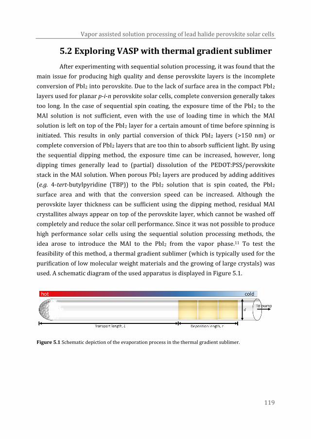
Vapor assisted solution processing of lead halide perovskite solar cells
119
5.2 Exploring VASP with thermal gradient sublimer
After experimenting with sequential solution processing, it was found that the
main issue for producing high quality and dense perovskite layers is the incomplete
conversion of PbI2 into perovskite. Due to the lack of surface area in the compact PbI2
layers used for planar p-i-n perovskite solar cells, complete conversion generally takes
too long. In the case of sequential spin coating, the exposure time of the PbI2 to the
MAI solution is not sufficient, even with the use of loading time in which the MAI
solution is left on top of the PbI2 layer for a certain amount of time before spinning is
initiated. This results in only partial conversion of thick PbI2 layers (>150 nm) or
complete conversion of PbI2 layers that are too thin to absorb sufficient light. By using
the sequential dipping method, the exposure time can be increased, however, long
dipping times generally lead to (partial) dissolution of the PEDOT:PSS/perovskite
stack in the MAI solution. When porous PbI2 layers are produced by adding additives
(e.g. 4-tert-butylpyridine (TBP)) to the PbI2 solution that is spin coated, the PbI2
surface area and with that the conversion speed can be increased. Although the
perovskite layer thickness can be sufficient using the dipping method, residual MAI
crystallites always appear on top of the perovskite layer, which cannot be washed off
completely and reduce the solar cell performance. Since it was not possible to produce
high performance solar cells using the sequential solution processing methods, the
idea arose to introduce the MAI to the PbI2 from the vapor phase.11 To test the
feasibility of this method, a thermal gradient sublimer (which is typically used for the
purification of low molecular weight materials and the growing of large crystals) was
used. A schematic diagram of the used apparatus is displayed in Figure 5.1.
Figure 5.1 Schematic depiction of the evaporation process in the thermal gradient sublimer.
Chapter 5
120
It consists of a glass tube that is under dynamic vacuum (~0.5 mbar). The
tube is placed inside the thermal gradient oven and is heated at one end and cooled
over its total length by a counter flow of cooling water. This creates a temperature
gradient over the length of the tube which can be influenced by the heating
temperature and the cooling water flow rate. Inside the glass tube, the MAI is placed at
the heated end behind some glass fiber wadding and PbI2 covered substrates are
positioned along the colder part of the tube. At the hot part of the tube, the MAI
evaporates and diffuses down the tube towards the PbI2 covered substrates. The
evaporation rate of MAI depends on the chamber pressure (Ph) and the temperature
of the tube at the location of the MAI according to equation 5.1.51, 52
𝛤 = 5.834 × 10⁻²√𝑀
𝑇c(𝑃e − 𝑃h) 5.1
Where Γ is the mass evaporation rate of MAI in g cm−2 s−1, M is the molecular weight of
MAI, Tc is the temperature of the evaporation source (crucible), Pe is the vapor
pressure of MAI (equilibrium pressure in Torr) at temperature Tc, and Ph is the
pressure inside the chamber (hydrostatic pressure in Torr). At a set chamber pressure
(Ph), the evaporation rate is therefore governed by the source temperature which
determines Pe. The evaporated MAI subsequently diffuses through the chamber. The
diffusion constant of a dilute gas is given by equation 5.2.53
𝐷g ∝𝑇3 2⁄
𝑃 5.2
In which Dg is the gas phase diffusion constant, T is the absolute temperature and P is
the pressure. At a certain point in the tube, the lower temperature causes the MAI
vapor to deposit onto the substrates placed there and the wall of the tube. When the
deposition occurs onto the PbI2 covered substrates and the conditions are right, MAI
can intercalate into the PbI2 layer and the PbI2 can be converted to perovskite,
evidenced by the gradual color change from yellow to dark brown. In this process, the
temperature dependent solid diffusion coefficient can often be described by equation
5.3.53
𝐷s = 𝐷0exp [−𝑄
𝑘𝑇] 5.3
Vapor assisted solution processing of lead halide perovskite solar cells
121
Where Ds is the gas diffusion constant, D0 the pre-exponential (frequency) factor, Q is
an activation energy, and k is Boltzmann's constant. The reaction mechanism to form
perovskite (CH3NH3PbI3) from the PbI2 and MAI (CH3NH3I) precursors is given by
equation 5.4. The reaction rate of perovskite formation (v) is dependent on the
concentration of both precursors ([CH3NH3I] and [PbI2]) and is given by equation 5.5
with n and m being the partial orders of the reaction (not necessarily equal to the
stoichiometric coefficients of the reaction). The temperature dependent rate constant
κ is given by the Arrhenius equation 5.6 with A a constant and Ea the activation
energy.54
PbI2 (s) + CH3NH3I (g) ⇄ CH3NH3PbI3 (s) 5.4
𝜈 = 𝜅 [CH3NH3I]𝑛 [PbI2]𝑚 5.5
𝜅 = 𝐴 exp [−𝐸a
𝑘𝑇] 5.6
When the pre-deposited PbI2 crystals are converted into perovskite crystals
by the intercalation of MAI, the crystallites undergo an expansion. The density and
unit cell volume of trigonal PbI2 have been reported to be 6.16 g cm−3 and 125.7 Å3
respectively while those of the tetragonal methylammonium lead triiodide (MAPbI3)
are 4.22 g cm−3 and 249.5 Å3.55 Therefore, the theoretically calculated volume
expansion factor (δ) should be ~2.0. When assuming no expansion in the plane due to
the compact nature of the PbI2 layer, the increase in the thickness of the PbI2 layer
upon conversion can also be expected to be a factor ~2.0.
In the initial experiments with the thermal gradient sublimer, the
temperature of the heater of the tube was varied to find a suitable temperature for the
evaporation of MAI and deposition onto the ~140 nm thick PbI2 covered substrates.
Here it was found that with a too high temperature of the heater (~160 to ~180 °C)
the deposition of MAI on top of the PbI2 coated substrates is too harsh. Creating MAI
crystallites on top of the PbI2 layer with hardly any conversion of the PbI2 layer to
perovskite resulting in non-functional solar cells (Figure 5.2). At these heater
temperatures, the temperature of the tube at the location of the samples is ~110 °C.

Chapter 5
122
Figure 5.2 Top view SEM images of perovskite films with excess MAI crystallites deposited on top of the
PbI2 layer. Samples were fabricated with the thermal gradient sublimer at a heater temperature of 180 °C
and a deposition time of 20 minutes. Scale bars are 50 µm (left) and 5 µm (right)
Lowering the heater temperature to ~140 °C reduces the MAI deposition rate
sufficiently to produce reasonable perovskite layers. Using this heater temperature,
the tube at the position of the 3rd sample is ~90 °C. In Figure 5.3 an example of the
samples before and after the deposition of MAI is displayed. From this example it is
seen that the samples that are closest to the MAI during the deposition are converted
to perovskite first. However, an excess of MAI is deposited on top of these samples
upon prolonged deposition. The samples farthest from the crucible remain almost
completely unconverted, because the MAI vapor does reach the far end of the tube
sufficiently as can been seen from the absence of the white MAI crystals deposited on
the inside of the glass tube. The result is that only one or two of the PbI2 layers are
converted sufficiently to perovskite without having excess MAI on top of them and
only these few produced perovskite layers perform well in a solar cell.
Porous PbI2 layers (~140 nm) were produced by adding TBP to the PbI2
solution (120 or 240 µl TBP mL−1 DMF) (Figure 5.4) and it was found that the easier
intercalation of MAI into the more porous PbI2 layer results in a larger number of
substrates that are converted sufficiently while not having excess MAI on top of the
perovskite layer (Figure 5.5). However still, only one or two of the perovskite layers
perform well in a solar cell. In Tables 5.1 and 5.2 the highest achieved efficiencies
using both the compact and porous PbI2 layers after optimization of the complete
evaporation process (deposition time and temperature, post deposition annealing,
and PbI2 layer thickness) are displayed, where substrate #1 is closest to the MAI.
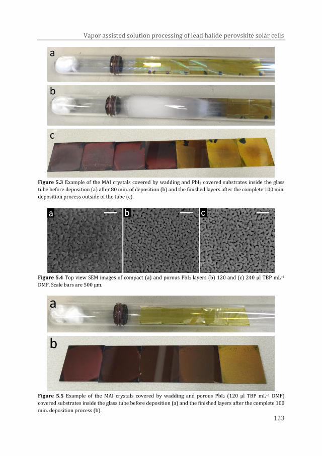
Vapor assisted solution processing of lead halide perovskite solar cells
123
Figure 5.3 Example of the MAI crystals covered by wadding and PbI2 covered substrates inside the glass
tube before deposition (a) after 80 min. of deposition (b) and the finished layers after the complete 100 min.
deposition process outside of the tube (c).
Figure 5.4 Top view SEM images of compact (a) and porous PbI2 layers (b) 120 and (c) 240 µl TBP mL−1
DMF. Scale bars are 500 µm.
Figure 5.5 Example of the MAI crystals covered by wadding and porous PbI2 (120 µl TBP mL−1 DMF)
covered substrates inside the glass tube before deposition (a) and the finished layers after the complete 100
min. deposition process (b).
a
b
c
a
b
Chapter 5
124
Table 5.1 Regular (fast) J-V characteristics of solar cells produced in the thermal gradient sublimer using
the optimal settings for the compact PbI2 layers. Values are averages and standard deviation of 4 cells on
one substrate.
Substrate No. JSC (mA cm−2) VOC (V) FF Pmax (%)
1 2.8 ± 2.4 0.88 ± 0.07 0.61 ± 0.06 1.4 ± 0.9
2 4.1 ± 2.5 0.95 ± 0.02 0.61 ± 0.05 2.3 ± 1.2
3 8.8 ± 1.9 0.96 ± 0.02 0.55 ± 0.19 4.9 ± 2.7
4 1.4 ± 0.2 0.73 ± 0.03 0.37 ± 0.04 0.4 ± 0.1
Record device 10.7 0.98 0.73 7.7
Table 5.2 Regular (fast) J-V characteristics of solar cells produced in the thermal gradient sublimer using
the optimal settings for the porous PbI2 layers. Values are averages and standard deviation of 4 cells on one
substrate.
Substrate No. JSC (mA cm−2) VOC (V) FF Pmax (%)
1 2.3 ± 0.6 0.84 ± 0.06 0.62 ± 0.14 1.3 ± 0.5
2 8.3 ± 1.4 0.87 ± 0.02 0.74 ± 0.03 5.4 ± 1.2
3 10.2 ± 1.4 0.70 ± 0.03 0.39 ± 0.06 2.8 ± 0.6
4 3.7 ± 0.5 0.33 ± 0.03 0.29 ± 0.00 0.4 ± 0.1
Record device 9.3 0.89 0.78 6.5
These exploratory experiments using the thermal gradient sublimer have
shown that PbI2 layers can be converted to perovskite with exposure to MAI vapor at
moderate temperatures and pressures. Although the solar cell efficiency that can be
achieved using the thermal gradient sublimation equipment is reasonable, the large
variation in the solar cell performance on one substrate and between substrates due
to the strong deposition gradient along the tube axis makes the equipment unsuitable
for reproducible and reliable experiments with a larger number of samples per batch.
In order to produce vapor assisted solution processed (VASP) perovskite solar cells on
larger scale (up to 9 substrates per batch) a VASP reactor was designed and produced,
based on the information gathered in the experiments using the thermal gradient
sublimer. The design of this reactor is discussed in section 5.3.
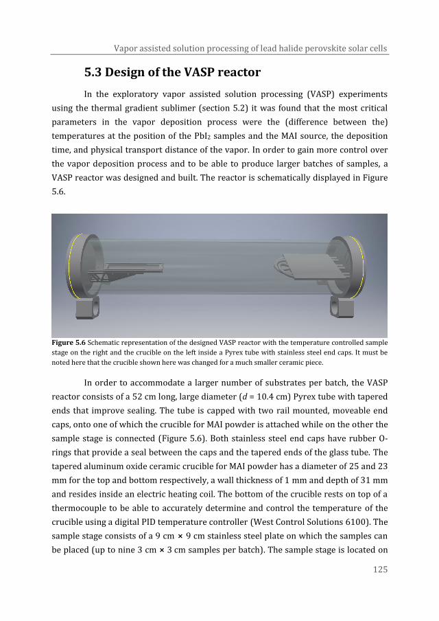
Vapor assisted solution processing of lead halide perovskite solar cells
125
5.3 Design of the VASP reactor
In the exploratory vapor assisted solution processing (VASP) experiments
using the thermal gradient sublimer (section 5.2) it was found that the most critical
parameters in the vapor deposition process were the (difference between the)
temperatures at the position of the PbI2 samples and the MAI source, the deposition
time, and physical transport distance of the vapor. In order to gain more control over
the vapor deposition process and to be able to produce larger batches of samples, a
VASP reactor was designed and built. The reactor is schematically displayed in Figure
5.6.
Figure 5.6 Schematic representation of the designed VASP reactor with the temperature controlled sample
stage on the right and the crucible on the left inside a Pyrex tube with stainless steel end caps. It must be
noted here that the crucible shown here was changed for a much smaller ceramic piece.
In order to accommodate a larger number of substrates per batch, the VASP
reactor consists of a 52 cm long, large diameter (d = 10.4 cm) Pyrex tube with tapered
ends that improve sealing. The tube is capped with two rail mounted, moveable end
caps, onto one of which the crucible for MAI powder is attached while on the other the
sample stage is connected (Figure 5.6). Both stainless steel end caps have rubber O-
rings that provide a seal between the caps and the tapered ends of the glass tube. The
tapered aluminum oxide ceramic crucible for MAI powder has a diameter of 25 and 23
mm for the top and bottom respectively, a wall thickness of 1 mm and depth of 31 mm
and resides inside an electric heating coil. The bottom of the crucible rests on top of a
thermocouple to be able to accurately determine and control the temperature of the
crucible using a digital PID temperature controller (West Control Solutions 6100). The
sample stage consists of a 9 cm ⨯ 9 cm stainless steel plate on which the samples can
be placed (up to nine 3 cm ⨯ 3 cm samples per batch). The sample stage is located on
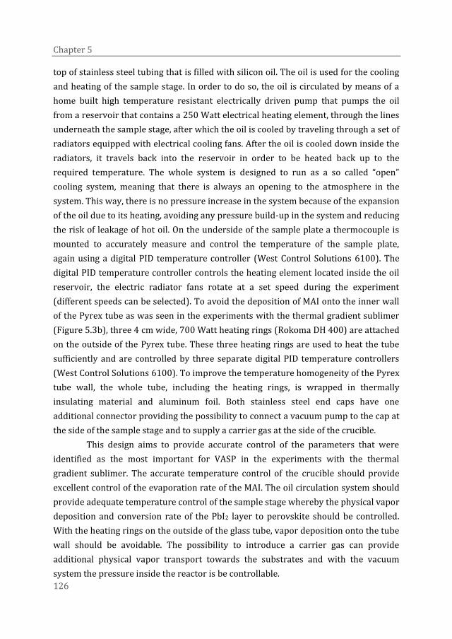
Chapter 5
126
top of stainless steel tubing that is filled with silicon oil. The oil is used for the cooling
and heating of the sample stage. In order to do so, the oil is circulated by means of a
home built high temperature resistant electrically driven pump that pumps the oil
from a reservoir that contains a 250 Watt electrical heating element, through the lines
underneath the sample stage, after which the oil is cooled by traveling through a set of
radiators equipped with electrical cooling fans. After the oil is cooled down inside the
radiators, it travels back into the reservoir in order to be heated back up to the
required temperature. The whole system is designed to run as a so called “open”
cooling system, meaning that there is always an opening to the atmosphere in the
system. This way, there is no pressure increase in the system because of the expansion
of the oil due to its heating, avoiding any pressure build-up in the system and reducing
the risk of leakage of hot oil. On the underside of the sample plate a thermocouple is
mounted to accurately measure and control the temperature of the sample plate,
again using a digital PID temperature controller (West Control Solutions 6100). The
digital PID temperature controller controls the heating element located inside the oil
reservoir, the electric radiator fans rotate at a set speed during the experiment
(different speeds can be selected). To avoid the deposition of MAI onto the inner wall
of the Pyrex tube as was seen in the experiments with the thermal gradient sublimer
(Figure 5.3b), three 4 cm wide, 700 Watt heating rings (Rokoma DH 400) are attached
on the outside of the Pyrex tube. These three heating rings are used to heat the tube
sufficiently and are controlled by three separate digital PID temperature controllers
(West Control Solutions 6100). To improve the temperature homogeneity of the Pyrex
tube wall, the whole tube, including the heating rings, is wrapped in thermally
insulating material and aluminum foil. Both stainless steel end caps have one
additional connector providing the possibility to connect a vacuum pump to the cap at
the side of the sample stage and to supply a carrier gas at the side of the crucible.
This design aims to provide accurate control of the parameters that were
identified as the most important for VASP in the experiments with the thermal
gradient sublimer. The accurate temperature control of the crucible should provide
excellent control of the evaporation rate of the MAI. The oil circulation system should
provide adequate temperature control of the sample stage whereby the physical vapor
deposition and conversion rate of the PbI2 layer to perovskite should be controlled.
With the heating rings on the outside of the glass tube, vapor deposition onto the tube
wall should be avoidable. The possibility to introduce a carrier gas can provide
additional physical vapor transport towards the substrates and with the vacuum
system the pressure inside the reactor is be controllable.
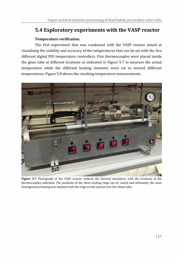
Vapor assisted solution processing of lead halide perovskite solar cells
127
5.4 Exploratory experiments with the VASP reactor
Temperature verification
The first experiment that was conducted with the VASP reactor aimed at
visualizing the stability and accuracy of the temperatures that can be set with the five
different digital PID temperature controllers. Five thermocouples were placed inside
the glass tube at different locations as indicated in Figure 5.7 to measure the actual
temperature while the different heating elements were set to several different
temperatures. Figure 5.8 shows the resulting temperature measurements.
Figure 5.7 Photograph of the VASP reactor without the thermal insulation, with the locations of the
thermocouples indicated. The positions of the three heating rings can be varied and ultimately, the most
homogeneous heating was attained with the rings evenly spaced over the whole tube.

Chapter 5
128
0 10 20 30 40 50 60 70 80 90 100 110 120 130 140 150 160
0
20
40
60
80
100
120
140
160
180
200
220
T1: 140 C
T2: 180 C
T5: 180 C
T1: 140 C
T2: 160 C
T5: 180 C
T1: 120 C
T2: 140 C
T5: 180 C
Te
mp
era
ture
(C
)
Time (min.)
T5: 180 C
T1: 120 C
T5: 180 C
T1 Sample stage
T2 Crucible
T3 Inner wall
T4 Inner wall
T5 Heating ring
0 10 20 30 40 50 60 70 80 90 100 110 120 130
0
20
40
60
80
100
120
140
160
180
200
220
Time (min.)
Te
mp
era
ture
(C
)
T1: 140 °C
T2: 140 °C
T5: 180 °C
T1: 120 °C
T2: 140 °C
T5: 180 °C
T1: 140 °C
T2: 160 °C
T5: 180 °CT1: 140 °C
T2: 180 °C
T5: 180 °C
T1: 140 °C
T5: 180 °C
T1 Sample stage
T2 Crucible
T3 Inner wall
T4 Inner wall
T5 Heating ring
Figure 5.8 Time dependent temperature measurements at different locations inside the VASP reactor as
indicated by Figure 5.7 (1 = top of sample stage, 2 = inside crucible, 3 = tube wall in between heating rings 1
and 2, 4 = tube wall in between heating rings 2 and 3, and 5 = at the position of heating ring 2). Set
temperature values are displayed in the rectangles.
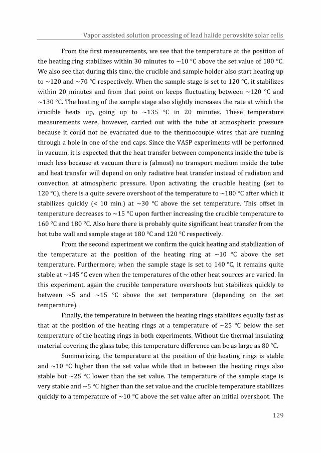
Vapor assisted solution processing of lead halide perovskite solar cells
129
From the first measurements, we see that the temperature at the position of
the heating ring stabilizes within 30 minutes to ~10 °C above the set value of 180 °C.
We also see that during this time, the crucible and sample holder also start heating up
to ~120 and ~70 °C respectively. When the sample stage is set to 120 °C, it stabilizes
within 20 minutes and from that point on keeps fluctuating between ~120 °C and
~130 °C. The heating of the sample stage also slightly increases the rate at which the
crucible heats up, going up to ~135 °C in 20 minutes. These temperature
measurements were, however, carried out with the tube at atmospheric pressure
because it could not be evacuated due to the thermocouple wires that are running
through a hole in one of the end caps. Since the VASP experiments will be performed
in vacuum, it is expected that the heat transfer between components inside the tube is
much less because at vacuum there is (almost) no transport medium inside the tube
and heat transfer will depend on only radiative heat transfer instead of radiation and
convection at atmospheric pressure. Upon activating the crucible heating (set to
120 °C), there is a quite severe overshoot of the temperature to ~180 °C after which it
stabilizes quickly (< 10 min.) at ~30 °C above the set temperature. This offset in
temperature decreases to ~15 °C upon further increasing the crucible temperature to
160 °C and 180 °C. Also here there is probably quite significant heat transfer from the
hot tube wall and sample stage at 180 °C and 120 °C respectively.
From the second experiment we confirm the quick heating and stabilization of
the temperature at the position of the heating ring at ~10 °C above the set
temperature. Furthermore, when the sample stage is set to 140 °C, it remains quite
stable at ~145 °C even when the temperatures of the other heat sources are varied. In
this experiment, again the crucible temperature overshoots but stabilizes quickly to
between ~5 and ~15 °C above the set temperature (depending on the set
temperature).
Finally, the temperature in between the heating rings stabilizes equally fast as
that at the position of the heating rings at a temperature of ~25 °C below the set
temperature of the heating rings in both experiments. Without the thermal insulating
material covering the glass tube, this temperature difference can be as large as 80 °C.
Summarizing, the temperature at the position of the heating rings is stable
and ~10 °C higher than the set value while that in between the heating rings also
stable but ~25 °C lower than the set value. The temperature of the sample stage is
very stable and ~5 °C higher than the set value and the crucible temperature stabilizes
quickly to a temperature of ~10 °C above the set value after an initial overshoot. The
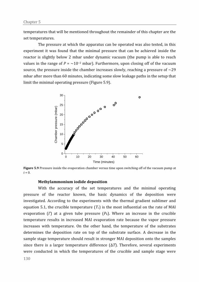
Chapter 5
130
temperatures that will be mentioned throughout the remainder of this chapter are the
set temperatures.
The pressure at which the apparatus can be operated was also tested, in this
experiment it was found that the minimal pressure that can be achieved inside the
reactor is slightly below 2 mbar under dynamic vacuum (the pump is able to reach
values in the range of P = ~10−2 mbar). Furthermore, upon closing off of the vacuum
source, the pressure inside the chamber increases slowly, reaching a pressure of ~29
mbar after more than 60 minutes, indicating some slow leakage paths in the setup that
limit the minimal operating pressure (Figure 5.9).
0 10 20 30 40 50 600
5
10
15
20
25
30
Ch
am
ber
pre
ssu
re (
mbar)
Time (minutes)
Figure 5.9 Pressure inside the evaporation chamber versus time upon switching off of the vacuum pump at
t = 0.
Methylammonium iodide deposition
With the accuracy of the set temperatures and the minimal operating
pressure of the reactor known, the basic dynamics of the deposition were
investigated. According to the experiments with the thermal gradient sublimer and
equation 5.1, the crucible temperature (Tc) is the most influential on the rate of MAI
evaporation (Γ) at a given tube pressure (Ph). Where an increase in the crucible
temperature results in increased MAI evaporation rate because the vapor pressure
increases with temperature. On the other hand, the temperature of the substrates
determines the deposition rate on top of the substrate surface. A decrease in the
sample stage temperature should result in stronger MAI deposition onto the samples
since there is a larger temperature difference (ΔT). Therefore, several experiments
were conducted in which the temperatures of the crucible and sample stage were
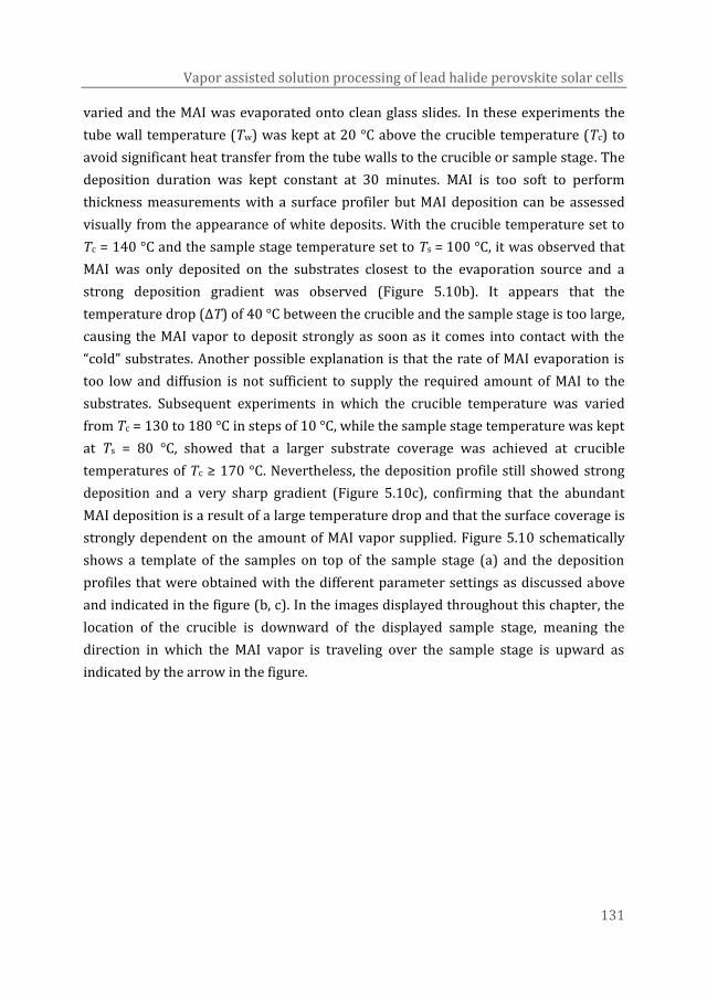
Vapor assisted solution processing of lead halide perovskite solar cells
131
varied and the MAI was evaporated onto clean glass slides. In these experiments the
tube wall temperature (Tw) was kept at 20 °C above the crucible temperature (Tc) to
avoid significant heat transfer from the tube walls to the crucible or sample stage. The
deposition duration was kept constant at 30 minutes. MAI is too soft to perform
thickness measurements with a surface profiler but MAI deposition can be assessed
visually from the appearance of white deposits. With the crucible temperature set to
Tc = 140 °C and the sample stage temperature set to Ts = 100 °C, it was observed that
MAI was only deposited on the substrates closest to the evaporation source and a
strong deposition gradient was observed (Figure 5.10b). It appears that the
temperature drop (ΔT) of 40 °C between the crucible and the sample stage is too large,
causing the MAI vapor to deposit strongly as soon as it comes into contact with the
“cold” substrates. Another possible explanation is that the rate of MAI evaporation is
too low and diffusion is not sufficient to supply the required amount of MAI to the
substrates. Subsequent experiments in which the crucible temperature was varied
from Tc = 130 to 180 °C in steps of 10 °C, while the sample stage temperature was kept
at Ts = 80 °C, showed that a larger substrate coverage was achieved at crucible
temperatures of Tc ≥ 170 °C. Nevertheless, the deposition profile still showed strong
deposition and a very sharp gradient (Figure 5.10c), confirming that the abundant
MAI deposition is a result of a large temperature drop and that the surface coverage is
strongly dependent on the amount of MAI vapor supplied. Figure 5.10 schematically
shows a template of the samples on top of the sample stage (a) and the deposition
profiles that were obtained with the different parameter settings as discussed above
and indicated in the figure (b, c). In the images displayed throughout this chapter, the
location of the crucible is downward of the displayed sample stage, meaning the
direction in which the MAI vapor is traveling over the sample stage is upward as
indicated by the arrow in the figure.
Chapter 5
132
Figure 5.10 Influence of crucible and substrate temperatures on the obtained deposition profile where a
darker color represents a thicker MAI layer.
Since a moderate and sufficiently homogeneous deposition profile could not
be obtained by varying only the crucible and sample stage temperatures, a flow of
nitrogen (N2) carrier gas was introduced. N2 was supplied via a pressure regulator and
needle valve to the end cap that holds the crucible. The reactor was evacuated to a
pressure of ~3.5 mbar and the pressure inside the tube was increased by opening the
N2 supply and regulated using the needle valve. The crucible and substrate
temperatures were set to 170 and 100 °C respectively and the deposition was
performed for 60 minutes at tube pressures of ~10, ~20, and ~50 mbar. Increasing
the tube pressure lowers the MAI evaporation rate and gas phase diffusion constant
according to equations 5.1 and 5.2, but the introduction of the carrier gas improves
the vapor flow towards the sample stage. At a tube pressure of ~10 mbar, a relatively
uniform deposition across all nine substrates was achieved (Figure 5.11 a). A uniform
deposition was not achieved with the higher operating pressures (Figure 5.11b and
5.11c). Noteworthy is the fact that in all cases, the left side area is largely not covered
with MAI. This corresponds to the location of the opening from which the tube is
evacuated (Figure 5.12), and will therefore probably experience the highest gas flow
rates. These high flow rates of cold N2 gas might be hindering deposition onto the
substrates due to cooling of the sample stage. Additionally, with the use of the N2
carrier gas, a large quantity of MAI was deposited on the walls of the tube as powder,
probably caused by deposition of the MAI vapor upon contact with the cold N2 carrier
gas. Therefore, a copper tube that is immersed in an oil bath that is kept at 70 °C was
added to the reactor in order to pre-heat the N2 carrier gas to a temperature of ~70 °C
before it enters the deposition chamber. The experiment at a chamber pressure of
~10 mbar was repeated, leading to a very similar deposition profile but without the
deposition of MAI powder on the inside of the tube. From these experiments, it is seen
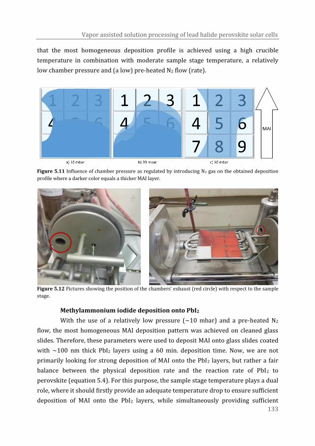
Vapor assisted solution processing of lead halide perovskite solar cells
133
that the most homogeneous deposition profile is achieved using a high crucible
temperature in combination with moderate sample stage temperature, a relatively
low chamber pressure and (a low) pre-heated N2 flow (rate).
Figure 5.11 Influence of chamber pressure as regulated by introducing N2 gas on the obtained deposition
profile where a darker color equals a thicker MAI layer.
Figure 5.12 Pictures showing the position of the chambers’ exhaust (red circle) with respect to the sample
stage.
Methylammonium iodide deposition onto PbI2
With the use of a relatively low pressure (~10 mbar) and a pre-heated N2
flow, the most homogeneous MAI deposition pattern was achieved on cleaned glass
slides. Therefore, these parameters were used to deposit MAI onto glass slides coated
with ~100 nm thick PbI2 layers using a 60 min. deposition time. Now, we are not
primarily looking for strong deposition of MAI onto the PbI2 layers, but rather a fair
balance between the physical deposition rate and the reaction rate of PbI2 to
perovskite (equation 5.4). For this purpose, the sample stage temperature plays a dual
role, where it should firstly provide an adequate temperature drop to ensure sufficient
deposition of MAI onto the PbI2 layers, while simultaneously providing sufficient

Chapter 5
134
thermal energy to provide the activation energy for reaction of PbI2 with MAI to
perovskite.56, 57 The resulting deposition and conversion profile showed that the area
in which the MAI deposition is very small, has turned into a nice dark brown
perovskite color (Figure 5.12 right). The area in which the MAI deposition is strongest
on the other hand, has turned into a red phase, which quickly turns white or
transparent after exposure to atmospheric conditions, indicating a strong instability of
the created material. Also post deposition annealing does not influence the
appearance of the red layer. A similar red color was observed on the samples that
were closest to the MAI source in the experiments with the thermal gradient sublimer
(Figures 5.3c and 5.5b). Indicating that the physical MAI deposition onto these
substrates is too strong and there is an imbalance in the deposition and conversion
processes, hindering the formation of the desired brown perovskite phase. X-ray
diffraction (XRD) measurements of the red and brown perovskite layers were
performed, showing firstly that the brown phase is indeed the desired perovskite
phase, displaying the characteristic (110) and (220) perovskite peaks at angles of
14.2° and 28.6° respectively, along with a small PbI2 peak at 12.6° (Figure 5.13).58, 59
The red phase does not show the characteristic perovskite peaks and the large peak at
11.4° could not be identified with the perovskite or any of the precursor materials.
10 20 30 40 50 60
(003)
Red phase Perovskite powder
Brown phase PbI2 powder
MAI powder
No
rma
lize
d in
ten
sity
2 ()
(110)
(200) (202)(424)
(334)
(404)(314)
(224)
(312)
(222)(220)
(008)
(001)(100)
(101)
(102)
(111) (103)(201)(002) (110) (004)
(113)(202)
Figure 5.13 Normalized X-ray diffraction patterns of the red and brown phases produced using the VASP
reactor along with powder references of the perovskite and precursor materials.
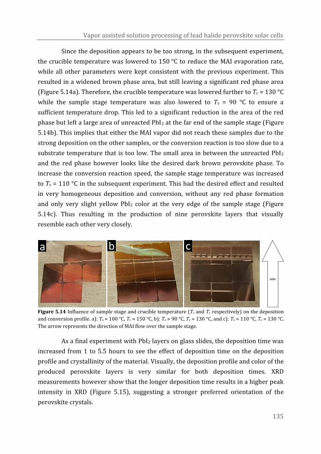
Vapor assisted solution processing of lead halide perovskite solar cells
135
Since the deposition appears to be too strong, in the subsequent experiment,
the crucible temperature was lowered to 150 °C to reduce the MAI evaporation rate,
while all other parameters were kept consistent with the previous experiment. This
resulted in a widened brown phase area, but still leaving a significant red phase area
(Figure 5.14a). Therefore, the crucible temperature was lowered further to Tc = 130 °C
while the sample stage temperature was also lowered to Ts = 90 °C to ensure a
sufficient temperature drop. This led to a significant reduction in the area of the red
phase but left a large area of unreacted PbI2 at the far end of the sample stage (Figure
5.14b). This implies that either the MAI vapor did not reach these samples due to the
strong deposition on the other samples, or the conversion reaction is too slow due to a
substrate temperature that is too low. The small area in between the unreacted PbI2
and the red phase however looks like the desired dark brown perovskite phase. To
increase the conversion reaction speed, the sample stage temperature was increased
to Ts = 110 °C in the subsequent experiment. This had the desired effect and resulted
in very homogeneous deposition and conversion, without any red phase formation
and only very slight yellow PbI2 color at the very edge of the sample stage (Figure
5.14c). Thus resulting in the production of nine perovskite layers that visually
resemble each other very closely.
Figure 5.14 Influence of sample stage and crucible temperature (Ts and Tc respectively) on the deposition
and conversion profile. a): Ts = 100 °C, Tc = 150 °C, b): Ts = 90 °C, Tc = 130 °C, and c): Ts = 110 °C, Tc = 130 °C.
The arrow represents the direction of MAI flow over the sample stage.
As a final experiment with PbI2 layers on glass slides, the deposition time was
increased from 1 to 5.5 hours to see the effect of deposition time on the deposition
profile and crystallinity of the material. Visually, the deposition profile and color of the
produced perovskite layers is very similar for both deposition times. XRD
measurements however show that the longer deposition time results in a higher peak
intensity in XRD (Figure 5.15), suggesting a stronger preferred orientation of the
perovskite crystals.
a b c
MAI
a b c
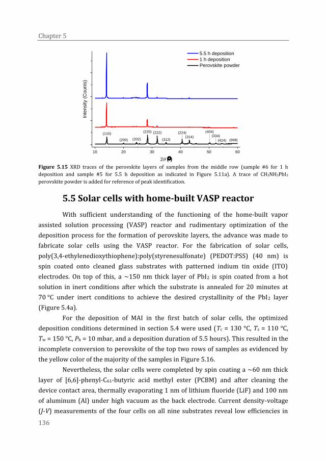
Chapter 5
136
10 20 30 40 50 60
5.5 h deposition
1 h deposition
Perovskite powder
Inte
nsity (
Coun
ts)
2 ()
(110)
(200) (202) (424)(314)
(312)
(222)(220) (224) (404)
(334)(008)
Figure 5.15 XRD traces of the perovskite layers of samples from the middle row (sample #6 for 1 h
deposition and sample #5 for 5.5 h deposition as indicated in Figure 5.11a). A trace of CH3NH3PbI3
perovskite powder is added for reference of peak identification.
5.5 Solar cells with home-built VASP reactor
With sufficient understanding of the functioning of the home-built vapor
assisted solution processing (VASP) reactor and rudimentary optimization of the
deposition process for the formation of perovskite layers, the advance was made to
fabricate solar cells using the VASP reactor. For the fabrication of solar cells,
poly(3,4-ethylenedioxythiophene):poly(styrenesulfonate) (PEDOT:PSS) (40 nm) is
spin coated onto cleaned glass substrates with patterned indium tin oxide (ITO)
electrodes. On top of this, a ~150 nm thick layer of PbI2 is spin coated from a hot
solution in inert conditions after which the substrate is annealed for 20 minutes at
70 °C under inert conditions to achieve the desired crystallinity of the PbI2 layer
(Figure 5.4a).
For the deposition of MAI in the first batch of solar cells, the optimized
deposition conditions determined in section 5.4 were used (Tc = 130 °C, Ts = 110 °C,
Tw = 150 °C, Ph = 10 mbar, and a deposition duration of 5.5 hours). This resulted in the
incomplete conversion to perovskite of the top two rows of samples as evidenced by
the yellow color of the majority of the samples in Figure 5.16.
Nevertheless, the solar cells were completed by spin coating a ~60 nm thick
layer of [6,6]‐phenyl‐C61‐butyric acid methyl ester (PCBM) and after cleaning the
device contact area, thermally evaporating 1 nm of lithium fluoride (LiF) and 100 nm
of aluminum (Al) under high vacuum as the back electrode. Current density-voltage
(J-V) measurements of the four cells on all nine substrates reveal low efficiencies in
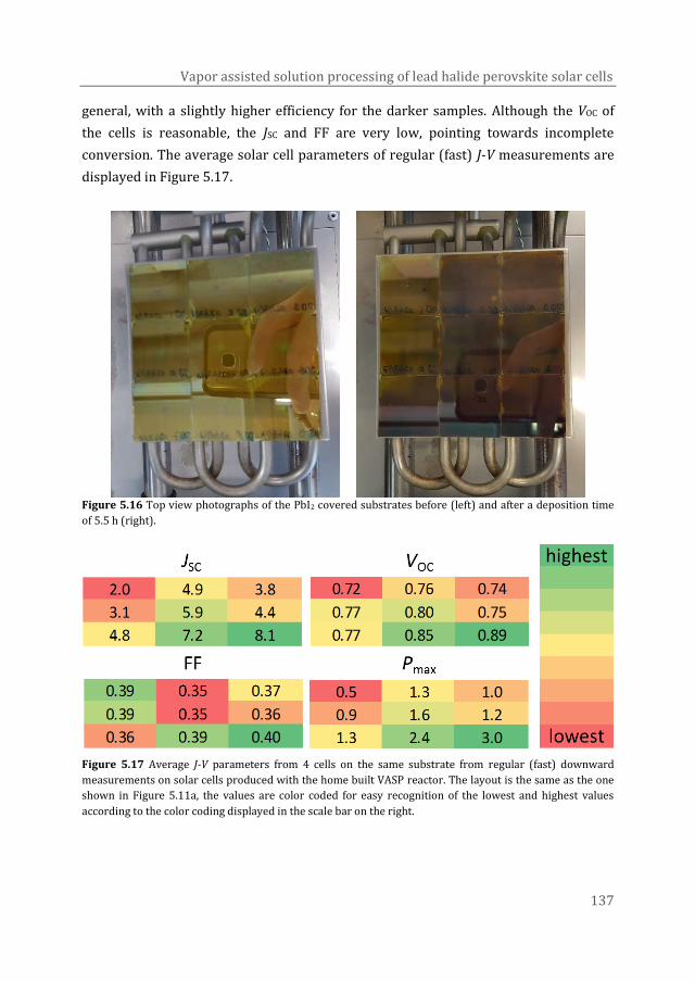
Vapor assisted solution processing of lead halide perovskite solar cells
137
general, with a slightly higher efficiency for the darker samples. Although the VOC of
the cells is reasonable, the JSC and FF are very low, pointing towards incomplete
conversion. The average solar cell parameters of regular (fast) J-V measurements are
displayed in Figure 5.17.
Figure 5.16 Top view photographs of the PbI2 covered substrates before (left) and after a deposition time
of 5.5 h (right).
Figure 5.17 Average J-V parameters from 4 cells on the same substrate from regular (fast) downward
measurements on solar cells produced with the home built VASP reactor. The layout is the same as the one
shown in Figure 5.11a, the values are color coded for easy recognition of the lowest and highest values
according to the color coding displayed in the scale bar on the right.

Chapter 5
138
XRD measurements on the darkest and highest performing device (sample 9)
and the most yellow and worst performing device (sample 1) confirm the incomplete
conversion of the PbI2 layers by showing very large PbI2 peaks and only very small
perovskite peaks in both cases (Figure 5.18). Indicating that in both samples, the
conversion is very small. Additionally, the appearance of selected PbI2 diffraction
peaks ((001) and (003)) suggests that the PbI2 layer has some preferential
orientation. Thickness measurements of the perovskite layers confirm the low
conversion with expansion factors of δ = 1.2 and 1.6 for substrates 1 and 9
respectively.
10 20 30 40 50 60
(003)
+
* Perovskite
(110)
*
*
+
Inte
nsity (
Coun
ts)
2 ()
sample 9
sample 1
+ PbI2
(001)
+
Figure 5.18 XRD traces of solar cells 1 and 9 produced using the VASP reactor, characteristic CH3NH3PbI3
and PbI2 peaks are indicated with an asterisk and plus sign respectively.
After varying the deposition parameters in several subsequent experiments, it
was found that the pressure inside the chamber has a large effect on the deposition
and conversion rate. Figure 5.19 shows several photographs that were taken during
the deposition process. After only 30 minutes of deposition, the samples have already
turned very faintly brown (Figure 5.19a). The color of the sample does however not
get much darker upon prolonged deposition up to 205 minutes (Figure 5.19b).
Lowering the chamber pressure from 10 mbar to 6 mbar, resulted in significantly
darker samples after only 40 minutes of additional deposition (Figure 5.19c). An
additional 110 minutes of deposition in which the pressure was varied between 2 and
6 mbar resulted in very dark perovskite layers (Figure 5.19d). Additionally, with this
variation of chamber pressure it was observed that when the chamber pressure is
reduced below ~4 mbar, deposition of MAI powder on top of the perovskite layers
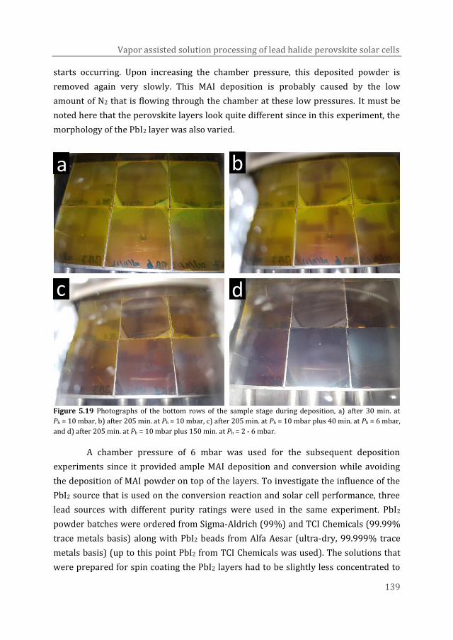
Vapor assisted solution processing of lead halide perovskite solar cells
139
starts occurring. Upon increasing the chamber pressure, this deposited powder is
removed again very slowly. This MAI deposition is probably caused by the low
amount of N2 that is flowing through the chamber at these low pressures. It must be
noted here that the perovskite layers look quite different since in this experiment, the
morphology of the PbI2 layer was also varied.
Figure 5.19 Photographs of the bottom rows of the sample stage during deposition, a) after 30 min. at
Ph = 10 mbar, b) after 205 min. at Ph = 10 mbar, c) after 205 min. at Ph = 10 mbar plus 40 min. at Ph = 6 mbar,
and d) after 205 min. at Ph = 10 mbar plus 150 min. at Ph = 2 - 6 mbar.
A chamber pressure of 6 mbar was used for the subsequent deposition
experiments since it provided ample MAI deposition and conversion while avoiding
the deposition of MAI powder on top of the layers. To investigate the influence of the
PbI2 source that is used on the conversion reaction and solar cell performance, three
lead sources with different purity ratings were used in the same experiment. PbI2
powder batches were ordered from Sigma-Aldrich (99%) and TCI Chemicals (99.99%
trace metals basis) along with PbI2 beads from Alfa Aesar (ultra-dry, 99.999% trace
metals basis) (up to this point PbI2 from TCI Chemicals was used). The solutions that
were prepared for spin coating the PbI2 layers had to be slightly less concentrated to
a b
c d
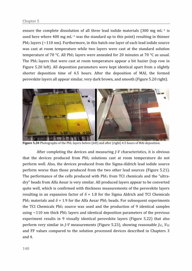
Chapter 5
140
ensure the complete dissolution of all three lead iodide materials (300 mg mL−1 is
used here where 400 mg mL−1 was the standard up to this point) resulting in thinner
PbI2 layers (~110 nm). Furthermore, in this batch one layer of each lead iodide source
was cast at room temperature while two layers were cast at the standard solution
temperature of 70 °C. All PbI2 layers were annealed for 20 minutes at 70 °C as usual.
The PbI2 layers that were cast at room temperature appear a bit hazier (top row in
Figure 5.20 left). All deposition parameters were kept identical apart from a slightly
shorter deposition time of 4.5 hours. After the deposition of MAI, the formed
perovskite layers all appear similar, very dark brown, and smooth (Figure 5.20 right).
Figure 5.20 Photographs of the PbI2 layers before (left) and after (right) 4.5 hours of MAI deposition.
After completing the devices and measuring J-V characteristics, it is obvious
that the devices produced from PbI2 solutions cast at room temperature do not
perform well. Also, the devices produced from the Sigma-Aldrich lead iodide source
perform worse than those produced from the two other lead sources (Figure 5.21).
The performance of the cells produced with PbI2 from TCI chemicals and the “ultra-
dry” beads from Alfa Aesar is very similar. All produced layers appear to be converted
quite well, which is confirmed with thickness measurements of the perovskite layers
resulting in an expansion factor of δ = 1.8 for the Sigma Aldrich and TCI Chemicals
PbI2 materials and δ = 1.9 for the Alfa Aesar PbI2 beads. For subsequent experiments
the TCI Chemicals PbI2 source was used and the production of 9 identical samples
using ~110 nm thick PbI2 layers and identical deposition parameters of the previous
experiment results in 9 visually identical perovskite layers (Figure 5.22) that also
perform very similar in J-V measurements (Figure 5.23), showing reasonable JSC, VOC
and FF values compared to the solution processed devices described in Chapters 3
and 4.
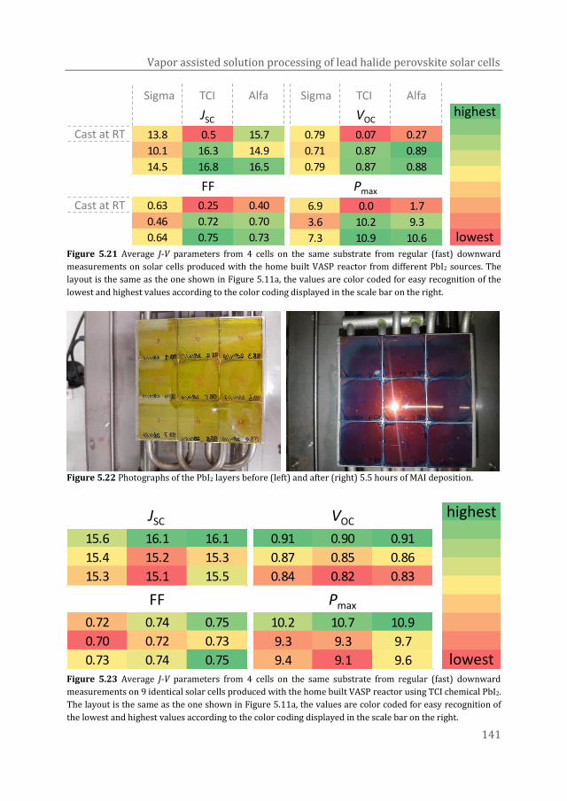
Vapor assisted solution processing of lead halide perovskite solar cells
141
Figure 5.21 Average J-V parameters from 4 cells on the same substrate from regular (fast) downward
measurements on solar cells produced with the home built VASP reactor from different PbI2 sources. The
layout is the same as the one shown in Figure 5.11a, the values are color coded for easy recognition of the
lowest and highest values according to the color coding displayed in the scale bar on the right.
Figure 5.22 Photographs of the PbI2 layers before (left) and after (right) 5.5 hours of MAI deposition.
Figure 5.23 Average J-V parameters from 4 cells on the same substrate from regular (fast) downward
measurements on 9 identical solar cells produced with the home built VASP reactor using TCI chemical PbI2.
The layout is the same as the one shown in Figure 5.11a, the values are color coded for easy recognition of
the lowest and highest values according to the color coding displayed in the scale bar on the right.
0.79 0.07 0.27
0.71 0.87 0.89
0.79 0.87 0.88
6.9 0.0 1.7
3.6 10.2 9.3
7.3 10.9 10.6
0.63 0.25 0.40
0.46 0.72 0.70
0.64 0.75 0.73
13.8 0.5 15.7
10.1 16.3 14.9
14.5 16.8 16.5
JSC VOC
FF Pmax
9
8
7
6
5
4
3
2
1lowest
highestSigma TCI Alfa Sigma TCI Alfa
Cast at RT
Cast at RT
15.6 16.1 16.1
15.4 15.2 15.3
15.3 15.1 15.5
0.91 0.90 0.91
0.87 0.85 0.86
0.84 0.82 0.83
0.72 0.74 0.75
0.70 0.72 0.73
0.73 0.74 0.75
10.2 10.7 10.9
9.3 9.3 9.7
9.4 9.1 9.6
JSC VOC
FF Pmax
9
8
7
6
5
4
3
2
1lowest
highest
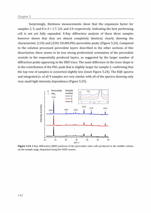
Chapter 5
142
Surprisingly, thickness measurements show that the expansion factor for
samples 2, 5, and 8 is δ = 1.7, 2.0, and 2.0 respectively. Indicating the best performing
cell is not yet fully expanded. X-Ray diffraction analysis of these three samples
however shows that they are almost completely identical, clearly showing the
characteristic (110) and (220) CH3NH3PbI3 perovskite peaks (Figure 5.24). Compared
to the solution processed perovskite layers described in the other sections of this
dissertation, there seems to be less strong preferential orientation of the perovskite
crystals in the sequentially produced layers, as suggested by the larger number of
diffraction peaks appearing in the XRD trace. The main difference in the trace shape is
in the contribution of the PbI2 peak that is slightly larger for sample 2, confirming that
the top row of samples is converted slightly less (inset Figure 5.24). The EQE spectra
and integrated JSC of all 9 samples are very similar with all of the spectra showing only
very small light intensity dependence (Figure 5.25).
10 15 20 25 30 35 40
12 13 14 15
* Perovskite
+ PbI2
(003)
+
(222)
*(202)
*
(200)
*
(220)
*
(110)
*
(001)
+
Inte
nsity (
Co
un
ts)
2()
Sample
number
2
5
8
Inte
nsity (
Co
unts
)
2()
PbI2
Figure 5.24 X-Ray diffraction (XRD) patterns of the perovskite solar cells produced in the middle column
on the sample stage, deposited using the VASP reactor.
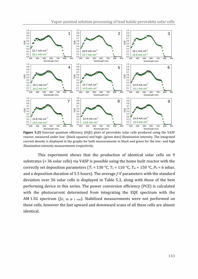
Vapor assisted solution processing of lead halide perovskite solar cells
143
300 400 500 600 700 800 9000.0
0.1
0.2
0.3
0.4
0.5
0.6
0.7
0.8
0.9
1.0
15.7 mA cm-2
15.1 mA cm-2
EQ
E
Wavelength (nm)
1
300 400 500 600 700 800 9000.0
0.1
0.2
0.3
0.4
0.5
0.6
0.7
0.8
0.9
1.0
2
16.0 mA cm-2
15.7 mA cm-2
EQ
E
Wavelength (nm)
300 400 500 600 700 800 9000.0
0.1
0.2
0.3
0.4
0.5
0.6
0.7
0.8
0.9
1.0
3
16.1 mA cm-2
15.8 mA cm-2
EQ
E
Wavelength (nm)
300 400 500 600 700 800 9000.0
0.1
0.2
0.3
0.4
0.5
0.6
0.7
0.8
0.9
1.0
4
15.1 mA cm-2
14.2 mA cm-2
EQ
E
Wavelength (nm)
300 400 500 600 700 800 9000.0
0.1
0.2
0.3
0.4
0.5
0.6
0.7
0.8
0.9
1.0
5
14.7 mA cm-2
14.0 mA cm-2
EQ
E
Wavelength (nm)
300 400 500 600 700 800 9000.0
0.1
0.2
0.3
0.4
0.5
0.6
0.7
0.8
0.9
1.0
6
14.9 mA cm-2
14.1 mA cm-2
EQ
E
Wavelength (nm)
300 400 500 600 700 800 9000.0
0.1
0.2
0.3
0.4
0.5
0.6
0.7
0.8
0.9
1.0
7
14.8 mA cm-2
14.0 mA cm-2
EQ
E
Wavelength (nm)
300 400 500 600 700 800 9000.0
0.1
0.2
0.3
0.4
0.5
0.6
0.7
0.8
0.9
1.0
8
14.4 mA cm-2
13.8 mA cm-2
EQ
E
Wavelength (nm)
300 400 500 600 700 800 9000.0
0.1
0.2
0.3
0.4
0.5
0.6
0.7
0.8
0.9
1.0
9
14.9 mA cm-2
14.4 mA cm-2
EQ
E
Wavelength (nm) Figure 5.25 External quantum efficiency (EQE) plots of perovskite solar cells produced using the VASP
reactor, measured under low- (black squares) and high- (green dots) illumination intensity. The integrated
current density is displayed in the graphs for both measurements in black and green for the low- and high
illumination intensity measurements respectively.
This experiment shows that the production of identical solar cells on 9
substrates (= 36 solar cells) via VASP is possible using the home built reactor with the
correctly set deposition parameters (Tc = 130 °C, Ts = 110 °C, Tw = 150 °C, Ph = 6 mbar,
and a deposition duration of 5.5 hours). The average J-V parameters with the standard
deviation over 36 solar cells is displayed in Table 5.3, along with those of the best
performing device in this series. The power conversion efficiency (PCE) is calculated
with the photocurrent determined from integrating the EQE spectrum with the
AM 1.5G spectrum (JSC, SR @ 1 sun). Stabilized measurements were not performed on
these cells, however the fast upward and downward scans of all these cells are almost
identical.
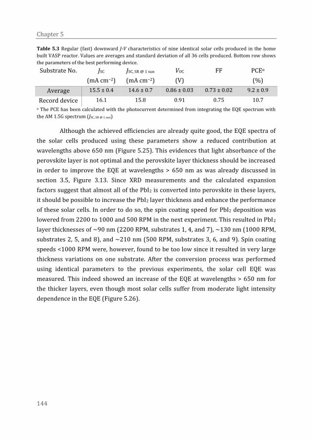
Chapter 5
144
Table 5.3 Regular (fast) downward J-V characteristics of nine identical solar cells produced in the home
built VASP reactor. Values are averages and standard deviation of all 36 cells produced. Bottom row shows
the parameters of the best performing device.
Substrate No. JSC
(mA cm−2)
JSC, SR @ 1 sun
(mA cm−2)
VOC
(V)
FF PCEα
(%)
Average 15.5 ± 0.4 14.6 ± 0.7 0.86 ± 0.03 0.73 ± 0.02 9.2 ± 0.9
Record device 16.1 15.8 0.91 0.75 10.7
α The PCE has been calculated with the photocurrent determined from integrating the EQE spectrum with
the AM 1.5G spectrum (JSC, SR @ 1 sun)
Although the achieved efficiencies are already quite good, the EQE spectra of
the solar cells produced using these parameters show a reduced contribution at
wavelengths above 650 nm (Figure 5.25). This evidences that light absorbance of the
perovskite layer is not optimal and the perovskite layer thickness should be increased
in order to improve the EQE at wavelengths > 650 nm as was already discussed in
section 3.5, Figure 3.13. Since XRD measurements and the calculated expansion
factors suggest that almost all of the PbI2 is converted into perovskite in these layers,
it should be possible to increase the PbI2 layer thickness and enhance the performance
of these solar cells. In order to do so, the spin coating speed for PbI2 deposition was
lowered from 2200 to 1000 and 500 RPM in the next experiment. This resulted in PbI2
layer thicknesses of ~90 nm (2200 RPM, substrates 1, 4, and 7), ~130 nm (1000 RPM,
substrates 2, 5, and 8), and ~210 nm (500 RPM, substrates 3, 6, and 9). Spin coating
speeds <1000 RPM were, however, found to be too low since it resulted in very large
thickness variations on one substrate. After the conversion process was performed
using identical parameters to the previous experiments, the solar cell EQE was
measured. This indeed showed an increase of the EQE at wavelengths > 650 nm for
the thicker layers, even though most solar cells suffer from moderate light intensity
dependence in the EQE (Figure 5.26).
Vapor assisted solution processing of lead halide perovskite solar cells
145
300 400 500 600 700 800 9000.0
0.1
0.2
0.3
0.4
0.5
0.6
0.7
0.8
0.9
1.0
15.5 mA cm-2
14.1 mA cm-2
EQ
E
Wavelength (nm)
1
300 400 500 600 700 800 9000.0
0.1
0.2
0.3
0.4
0.5
0.6
0.7
0.8
0.9
1.0
17.5 mA cm-2
16.6 mA cm-2
EQ
E
Wavelength (nm)
2
300 400 500 600 700 800 9000.0
0.1
0.2
0.3
0.4
0.5
0.6
0.7
0.8
0.9
1.0
17.7 mA cm-2
12.3 mA cm-2
EQ
E
Wavelength (nm)
3
300 400 500 600 700 800 9000.0
0.1
0.2
0.3
0.4
0.5
0.6
0.7
0.8
0.9
1.0
15.3 mA cm-2
12.9 mA cm-2
EQ
E
Wavelength (nm)
4
300 400 500 600 700 800 9000.0
0.1
0.2
0.3
0.4
0.5
0.6
0.7
0.8
0.9
1.0
17.3 mA cm-2
15.8 mA cm-2
EQ
E
Wavelength (nm)
5
300 400 500 600 700 800 9000.0
0.1
0.2
0.3
0.4
0.5
0.6
0.7
0.8
0.9
1.0
21.8 mA cm-2
20.4 mA cm-2
EQ
E
Wavelength (nm)
6
300 400 500 600 700 800 9000.0
0.1
0.2
0.3
0.4
0.5
0.6
0.7
0.8
0.9
1.0
15.6 mA cm-2
13.8 mA cm-2
EQ
E
Wavelength (nm)
7
300 400 500 600 700 800 9000.0
0.1
0.2
0.3
0.4
0.5
0.6
0.7
0.8
0.9
1.0
17.0 mA cm-2
15.8 mA cm-2
EQ
E
Wavelength (nm)
8
300 400 500 600 700 800 9000.0
0.1
0.2
0.3
0.4
0.5
0.6
0.7
0.8
0.9
1.0
19.4 mA cm-2
17.6 mA cm-2
EQ
E
Wavelength (nm)
9
Figure 5.26 External quantum efficiency (EQE) plots of perovskite solar cells produced using the VASP
reactor, measured under low (black squares) and high (green dots) illumination intensity. The integrated
current density is displayed in the graphs for both measurements in black and green for the low and high
illumination intensity measurements respectively.
From XRD analysis on the top and bottom row of substrates, the bottom row
of substrates seem to be completely converted, while plenty of PbI2 remains in the
substrates on the top row (Figure 5.27). However, this residual PbI2 apparently does
not have a negative influence on the device performance. Additionally, the thicker PbI2
layers appear to have more unconverted PbI2 looking at the perovskite to PbI2 peak
height ratio. There is no difference in the perovskite peak intensity for the samples on
the bottom row, even though the thickness measurements indicate the perovskite
layer thicknesses are different (~210, ~310, and ~410 nm for substrates 7, 8, and 9
respectively) and the calculated expansion factors: δ = 2.3 (#7), δ = 2.3 (#8), and δ
=1.9 (#9) indicate substantial conversion in all cases. The XRD results again show a
preferential orientation in the PbI2 layers and lower preferential orientation in the
perovskite layers compared to their solution processed counterparts.

Chapter 5
146
The solar cell characteristics show that the performance of the reference cells
is somewhat lower due to the slightly thinner PbI2 layer, but the thickest perovskite
layers do not perform well at all (Figure 5.28). This is most likely related to the large
variation in thickness of these PbI2 layers. The large difference between the
determined JSC in EQE and J-V measurements however cannot be explained.
10 15 20 25 30 35 400
10000
20000
30000
40000
50000
60000
(003)
+(222)
*
(220)
*
(202)
*
(200)
*
(110)
*
(001)
+
Inte
nsity (
Counts
)
2()
1 + PbI2
* Perovskite
10 15 20 25 30 35 400
10000
20000
30000
40000
50000
60000
Inte
nsity (
Counts
)
2()
2
(003)
+(222)
*
(220)
*(202)
*(200)
*
(110)
*
(001)
+
+ PbI2
* Perovskite
10 15 20 25 30 35 400
10000
20000
30000
40000
50000
60000
Inte
nsity (
Counts
)
2()
3
(003)
+(222)
*
(220)
*(202)
*(200)
*
(110)
*
(001)
+
+ PbI2
* Perovskite
10 15 20 25 30 35 400
10000
20000
30000
40000
50000
60000
Inte
nsity (
Counts
)
2()
7
(003)
+(222)
*
(220)
*(202)
*(200)
*
(110)
*
(001)
+
+ PbI2
* Perovskite
10 15 20 25 30 35 400
10000
20000
30000
40000
50000
60000
Inte
nsity (
Counts
)
2()
8
(003)
+(222)
*(220)
*(202)
*
(200)
*
(110)
*
(001)
+
+ PbI2
* Perovskite
10 15 20 25 30 35 400
10000
20000
30000
40000
50000
60000
Inte
nsity (
Counts
)
2()
9
(003)
+
(222)
*
(220)
*(202)
*
(200)
*
(110)
*
(001)
+
+ PbI2
* Perovskite
Figure 5.27 X-Ray diffraction (XRD) traces of the perovskite solar cells produced on the top and bottom
row of the sample stage using the VASP reactor.
Figure 5.28 Average J-V parameters from 4 cells on the same substrate from regular (fast) downward
measurements on solar cells produced with the home built VASP setup. The layout is the same as the one
shown in Figure 5.11a, the values are color coded for easy recognition of the lowest and highest values
according to the color coding displayed in the scale bar on the right.
13.1 14.6 5.9
13.0 15.5 9.6
13.0 14.3 7.4
0.94 0.94 0.34
0.89 0.88 0.25
0.85 0.84 0.24
0.68 0.66 0.33
0.68 0.71 0.34
0.69 0.71 0.32
8.3 9.1 1.6
7.8 9.7 1.0
7.6 8.6 0.6
JSC VOC
FF Pmax
9
8
7
6
5
4
3
2
1lowest
highest90 130 210 90 130 210
PbI2 thickness (nm) PbI2 thickness (nm)

Vapor assisted solution processing of lead halide perovskite solar cells
147
Alternative attempts to increase the thickness of the PbI2 layer by increasing
the solution concentration yielded similar results. PbI2 layer thicknesses of ~150,
~230, and ~390 nm were produced by spin coating (1000 RPM) 300, 400, and 500 mg
mL−1 solutions respectively. After conversion, the perovskite layer thicknesses were
~290 nm (δ = 1.9), ~410 nm (δ = 1.8), and ~540 nm (δ = 1.4) indicating significant
conversion except for the 390 nm thick PbI2 layers. J-V measurements show similar
performance for the 290 and 410 nm thick perovskite layers and very low
performance for the 540 nm perovskite layers (Figure 5.29).
Figure 5.29 Average J-V parameters from 4 cells on the same substrate from regular (fast) downward
measurements on solar cells produced with the VASP reactor. The layout is the same as the one shown in
Figure 5.11a, the values are color coded for easy recognition of the lowest and highest values according to
the color coding displayed in the scale bar on the right.
EQE measurement results also show very similar profiles with little light
intensity dependence for the bottom row ~290 and ~410 nm thick perovskite layers
(Figure 5.30). The ~540 nm thick perovskite layers show a low EQE with large light
intensity dependence. It is remarkable that the EQE profile of the 410 nm thick
perovskite layer is so similar to that of the much thinner ~290 nm perovskite layer,
even though the expansion factor indicates almost complete conversion. Attempts
were made to improve the conversion of these thicker layers by increasing the
porosity of the PbI2 layers with the addition of TBP to the PbI2 solution. This however
had no significant effect on conversion of the PbI2 layer or the device performance.
Therefore, the ~140 nm thick PbI2 layer (300 mg mL−1, 1000 RPM) gives the best
device performance and was used for subsequent experiments.
10.0 12.2 10.7
16.7 16.2 13.7
17.9 18.3 15.5
0.94 0.93 0.50
0.87 0.90 0.58
0.89 0.86 0.50
0.48 0.41 0.38
0.64 0.64 0.42
0.75 0.73 0.49
4.5 4.8 1.9
9.2 9.2 3.2
11.9 11.5 3.9
JSC VOC
FF Pmax
9
8
7
6
5
4
3
2
1lowest
highest150 230 390 150 230 390
PbI2 thickness (nm) PbI2 thickness (nm)
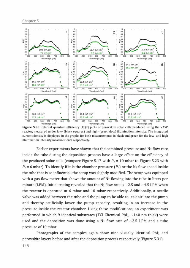
Chapter 5
148
300 400 500 600 700 800 9000.0
0.1
0.2
0.3
0.4
0.5
0.6
0.7
0.8
0.9
1.0
1
10.6 mA cm-2
7.2 mA cm-2
EQ
E
Wavelength (nm)
300 400 500 600 700 800 9000.0
0.1
0.2
0.3
0.4
0.5
0.6
0.7
0.8
0.9
1.0
2
13.7 mA cm-2
9.7 mA cm-2
EQ
E
Wavelength (nm)
300 400 500 600 700 800 9000.0
0.1
0.2
0.3
0.4
0.5
0.6
0.7
0.8
0.9
1.0
3
12.4 mA cm-2
8.1 mA cm-2
EQ
E
Wavelength (nm)
300 400 500 600 700 800 9000.0
0.1
0.2
0.3
0.4
0.5
0.6
0.7
0.8
0.9
1.0
4
16.9 mA cm-2
15.5 mA cm-2
EQ
E
Wavelength (nm)
300 400 500 600 700 800 9000.0
0.1
0.2
0.3
0.4
0.5
0.6
0.7
0.8
0.9
1.0
5
17.4 mA cm-2
15.5 mA cm-2
EQ
E
Wavelength (nm)
300 400 500 600 700 800 9000.0
0.1
0.2
0.3
0.4
0.5
0.6
0.7
0.8
0.9
1.0
6
14.3 mA cm-2
16.3 mA cm-2
EQ
E
Wavelength (nm)
300 400 500 600 700 800 9000.0
0.1
0.2
0.3
0.4
0.5
0.6
0.7
0.8
0.9
1.0
7
18.8 mA cm-2
17.8 mA cm-2
EQ
E
Wavelength (nm)
300 400 500 600 700 800 9000.0
0.1
0.2
0.3
0.4
0.5
0.6
0.7
0.8
0.9
1.0
8
19.1 mA cm-2
18.2 mA cm-2
EQ
E
Wavelength (nm)
300 400 500 600 700 800 9000.0
0.1
0.2
0.3
0.4
0.5
0.6
0.7
0.8
0.9
1.0
18.2 mA cm-2
15.8 mA cm-2
EQ
E
Wavelength (nm)
9
Figure 5.30 External quantum efficiency (EQE) plots of perovskite solar cells produced using the VASP
reactor, measured under low- (black squares) and high- (green dots) illumination intensity. The integrated
current density is displayed in the graphs for both measurements in black and green for the low- and high
illumination intensity measurements respectively.
Earlier experiments have shown that the combined pressure and N2 flow rate
inside the tube during the deposition process have a large effect on the efficiency of
the produced solar cells (compare Figure 5.17 with Ph = 10 mbar to Figure 5.23 with
Ph = 6 mbar). To identify if it is the chamber pressure (Ph) or the N2 flow speed inside
the tube that is so influential, the setup was slightly modified. The setup was equipped
with a gas flow meter that shows the amount of N2 flowing into the tube in liters per
minute (LPM). Initial testing revealed that the N2 flow rate is ~2.5 and ~4.5 LPM when
the reactor is operated at 6 mbar and 10 mbar respectively. Additionally, a needle
valve was added between the tube and the pump to be able to leak air into the pump
and thereby artificially lower the pump capacity, resulting in an increase in the
pressure inside the reactor chamber. Using these modifications, an experiment was
performed in which 9 identical substrates (TCI Chemical PbI2, ~140 nm thick) were
used and the deposition was done using a N2 flow rate of ~2.5 LPM and a tube
pressure of 10 mbar.
Photographs of the samples again show nine visually identical PbI2 and
perovskite layers before and after the deposition process respectively (Figure 5.31).
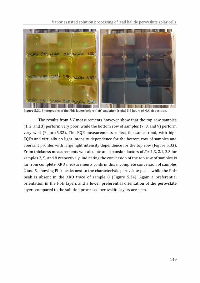
Vapor assisted solution processing of lead halide perovskite solar cells
149
Figure 5.31 Photographs of the PbI2 layers before (left) and after (right) 5.5 hours of MAI deposition.
The results from J-V measurements however show that the top row samples
(1, 2, and 3) perform very poor, while the bottom row of samples (7, 8, and 9) perform
very well (Figure 5.32). The EQE measurements reflect the same trend, with high
EQEs and virtually no light intensity dependence for the bottom row of samples and
aberrant profiles with large light intensity dependence for the top row (Figure 5.33).
From thickness measurements we calculate an expansion factors of δ = 1.3, 2.1, 2.3 for
samples 2, 5, and 8 respectively. Indicating the conversion of the top row of samples is
far from complete. XRD measurements confirm this incomplete conversion of samples
2 and 5, showing PbI2 peaks next to the characteristic perovskite peaks while the PbI2
peak is absent in the XRD trace of sample 8 (Figure 5.34). Again a preferential
orientation in the PbI2 layers and a lower preferential orientation of the perovskite
layers compared to the solution processed perovskite layers are seen.
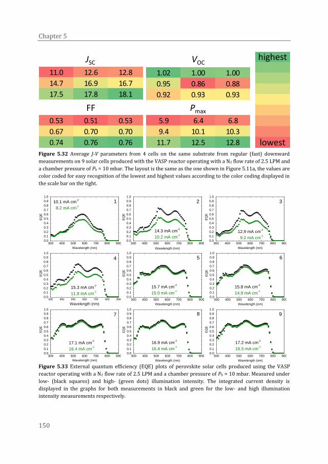
Chapter 5
150
Figure 5.32 Average J-V parameters from 4 cells on the same substrate from regular (fast) downward
measurements on 9 solar cells produced with the VASP reactor operating with a N2 flow rate of 2.5 LPM and
a chamber pressure of Ph = 10 mbar. The layout is the same as the one shown in Figure 5.11a, the values are
color coded for easy recognition of the lowest and highest values according to the color coding displayed in
the scale bar on the tight.
300 400 500 600 700 800 9000.0
0.1
0.2
0.3
0.4
0.5
0.6
0.7
0.8
0.9
1.0
10.1 mA cm-2
8.2 mA cm-2
EQ
E
Wavelength (nm)
1
300 400 500 600 700 800 9000.0
0.1
0.2
0.3
0.4
0.5
0.6
0.7
0.8
0.9
1.0
14.3 mA cm-2
10.2 mA cm-2
EQ
E
Wavelength (nm)
2
300 400 500 600 700 800 9000.0
0.1
0.2
0.3
0.4
0.5
0.6
0.7
0.8
0.9
1.0
12.9 mA cm-2
9.2 mA cm-2
EQ
E
Wavelength (nm)
3
300 400 500 600 700 800 9000.0
0.1
0.2
0.3
0.4
0.5
0.6
0.7
0.8
0.9
1.0
15.3 mA cm-2
11.8 mA cm-2
EQ
E
Wavelength (nm)
4
300 400 500 600 700 800 9000.0
0.1
0.2
0.3
0.4
0.5
0.6
0.7
0.8
0.9
1.0
15.7 mA cm-2
15.0 mA cm-2
EQ
E
Wavelength (nm)
5
300 400 500 600 700 800 9000.0
0.1
0.2
0.3
0.4
0.5
0.6
0.7
0.8
0.9
1.0
15.8 mA cm-2
14.9 mA cm-2
EQ
E
Wavelength (nm)
6
300 400 500 600 700 800 9000.0
0.1
0.2
0.3
0.4
0.5
0.6
0.7
0.8
0.9
1.0
17.1 mA cm-2
16.4 mA cm-2
EQ
E
Wavelength (nm)
7
300 400 500 600 700 800 9000.0
0.1
0.2
0.3
0.4
0.5
0.6
0.7
0.8
0.9
1.0
16.9 mA cm-2
16.4 mA cm-2
EQ
E
Wavelength (nm)
8
300 400 500 600 700 800 9000.0
0.1
0.2
0.3
0.4
0.5
0.6
0.7
0.8
0.9
1.0
17.2 mA cm-2
16.5 mA cm-2
EQ
E
Wavelength (nm)
9
Figure 5.33 External quantum efficiency (EQE) plots of perovskite solar cells produced using the VASP
reactor operating with a N2 flow rate of 2.5 LPM and a chamber pressure of Ph = 10 mbar. Measured under
low- (black squares) and high- (green dots) illumination intensity. The integrated current density is
displayed in the graphs for both measurements in black and green for the low- and high illumination
intensity measurements respectively.
11.0 12.6 12.8
14.7 16.9 16.7
17.5 17.8 18.1
1.02 1.00 1.00
0.95 0.86 0.88
0.92 0.93 0.93
0.53 0.51 0.53
0.67 0.70 0.70
0.74 0.76 0.76
5.9 6.4 6.8
9.4 10.1 10.3
11.7 12.5 12.8
JSC VOC
FF Pmax
9
8
7
6
5
4
3
2
1lowest
highest
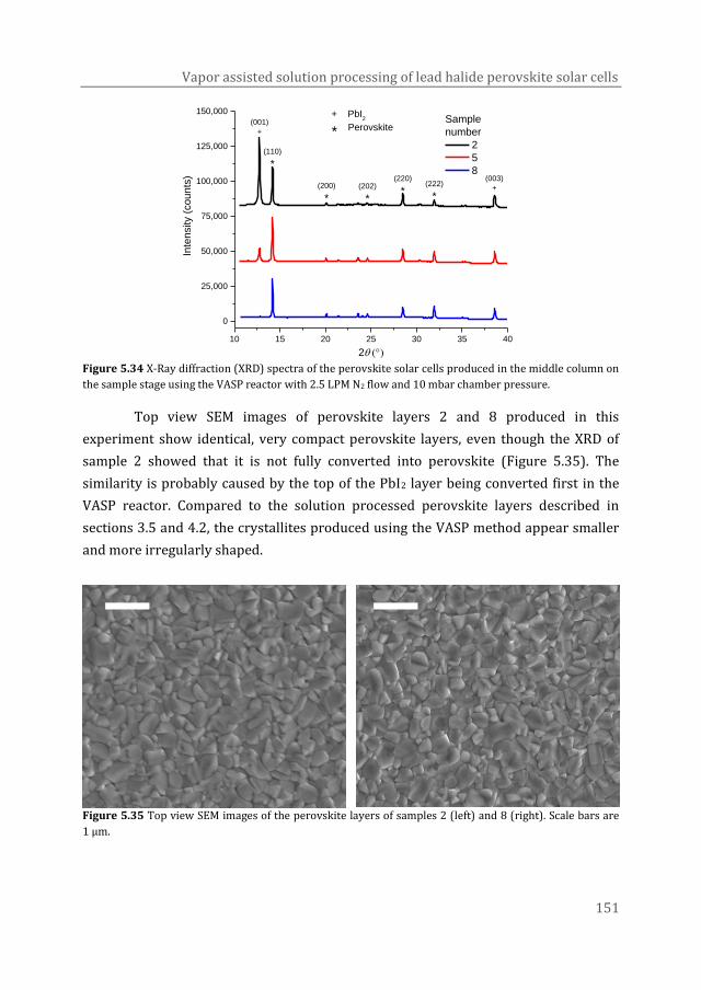
Vapor assisted solution processing of lead halide perovskite solar cells
151
10 15 20 25 30 35 40
0
25,000
50,000
75,000
100,000
125,000
150,000
* Perovskite
+ PbI2
Inte
nsity (
co
un
ts)
2()
Sample
number
2
5
8(003)
+(222)
*
(220)
*(202)
*
(200)
*
(110)
*
(001)
+
Figure 5.34 X-Ray diffraction (XRD) spectra of the perovskite solar cells produced in the middle column on
the sample stage using the VASP reactor with 2.5 LPM N2 flow and 10 mbar chamber pressure.
Top view SEM images of perovskite layers 2 and 8 produced in this
experiment show identical, very compact perovskite layers, even though the XRD of
sample 2 showed that it is not fully converted into perovskite (Figure 5.35). The
similarity is probably caused by the top of the PbI2 layer being converted first in the
VASP reactor. Compared to the solution processed perovskite layers described in
sections 3.5 and 4.2, the crystallites produced using the VASP method appear smaller
and more irregularly shaped.
Figure 5.35 Top view SEM images of the perovskite layers of samples 2 (left) and 8 (right). Scale bars are
1 µm.
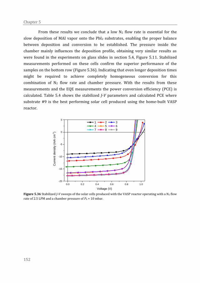
Chapter 5
152
From these results we conclude that a low N2 flow rate is essential for the
slow deposition of MAI vapor onto the PbI2 substrates, enabling the proper balance
between deposition and conversion to be established. The pressure inside the
chamber mainly influences the deposition profile, obtaining very similar results as
were found in the experiments on glass slides in section 5.4, Figure 5.11. Stabilized
measurements performed on these cells confirm the superior performance of the
samples on the bottom row (Figure 5.36). Indicating that even longer deposition times
might be required to achieve completely homogeneous conversion for this
combination of N2 flow rate and chamber pressure. With the results from these
measurements and the EQE measurements the power conversion efficiency (PCE) is
calculated. Table 5.4 shows the stabilized J-V parameters and calculated PCE where
substrate #9 is the best performing solar cell produced using the home-built VASP
reactor.
0.0 0.2 0.4 0.6 0.8 1.0
-20
-15
-10
-5
0
5
Curr
en
t de
nsity (
mA
cm
-2)
Voltage (V)
1 2 3
4 5 6
7 8 9
Figure 5.36 Stabilized J-V sweeps of the solar cells produced with the VASP reactor operating with a N2 flow
rate of 2.5 LPM and a chamber pressure of Ph = 10 mbar.
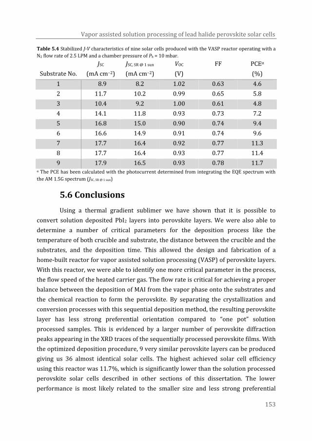
Vapor assisted solution processing of lead halide perovskite solar cells
153
Table 5.4 Stabilized J-V characteristics of nine solar cells produced with the VASP reactor operating with a
N2 flow rate of 2.5 LPM and a chamber pressure of Ph = 10 mbar.
Substrate No.
JSC
(mA cm−2)
JSC, SR @ 1 sun
(mA cm−2)
VOC
(V)
FF PCEα
(%)
1 8.9 8.2 1.02 0.63 4.6
2 11.7 10.2 0.99 0.65 5.8
3 10.4 9.2 1.00 0.61 4.8
4 14.1 11.8 0.93 0.73 7.2
5 16.8 15.0 0.90 0.74 9.4
6 16.6 14.9 0.91 0.74 9.6
7 17.7 16.4 0.92 0.77 11.3
8 17.7 16.4 0.93 0.77 11.4
9 17.9 16.5 0.93 0.78 11.7 α The PCE has been calculated with the photocurrent determined from integrating the EQE spectrum with
the AM 1.5G spectrum (JSC, SR @ 1 sun)
5.6 Conclusions
Using a thermal gradient sublimer we have shown that it is possible to
convert solution deposited PbI2 layers into perovskite layers. We were also able to
determine a number of critical parameters for the deposition process like the
temperature of both crucible and substrate, the distance between the crucible and the
substrates, and the deposition time. This allowed the design and fabrication of a
home-built reactor for vapor assisted solution processing (VASP) of perovskite layers.
With this reactor, we were able to identify one more critical parameter in the process,
the flow speed of the heated carrier gas. The flow rate is critical for achieving a proper
balance between the deposition of MAI from the vapor phase onto the substrates and
the chemical reaction to form the perovskite. By separating the crystallization and
conversion processes with this sequential deposition method, the resulting perovskite
layer has less strong preferential orientation compared to “one pot” solution
processed samples. This is evidenced by a larger number of perovskite diffraction
peaks appearing in the XRD traces of the sequentially processed perovskite films. With
the optimized deposition procedure, 9 very similar perovskite layers can be produced
giving us 36 almost identical solar cells. The highest achieved solar cell efficiency
using this reactor was 11.7%, which is significantly lower than the solution processed
perovskite solar cells described in other sections of this dissertation. The lower
performance is most likely related to the smaller size and less strong preferential
Chapter 5
154
orientation of the perovskite crystals in the solar cells produced using the VASP
reactor. Furthermore, a gradient in the conversion and with that the solar cell
performance is often seen along the axis of the tube. This is most likely related to the
combination of set temperatures, flow speed and deposition time and can most likely
be removed by further optimization of the deposition process.
The efficiency of the solar cells produced using this VASP setup can surely be
increased further and come close to that of its solution processed counterparts with
further optimization of the production process and the reactor itself. Even the
production of 36 identical high efficiency solar cells is probably possible using this
equipment. However, the production process is lengthy and with further optimization
the reaction time might even exceed the 5.5 hours that were used here. Although the
reproducibility of the method is good, this will still result in only 9 substrates (36
solar cells) per produced batch of solar cells. Furthermore, the solar cell performance
will probably still suffer from the lower degree of preferred orientation of the
perovskite crystals compared to that of the solution processed solar cells, potentially
limiting the device performance even after full optimization. Therefore, although we
have learned from the experiments working with this VASP reactor, the possibilities of
using this setup for larger scale production of highly efficient solar cells is not without
challenges. It does however show the opportunity of upscaling for this method and is
helpful towards the development of large scale VASP production processes.
Vapor assisted solution processing of lead halide perovskite solar cells
155
5.7 Experimental
Glass slides were cleaned by scrubbing in a solution of sodium dodecyl sulfate
(SDS, Acros, 99%) in filtered water (Milli-Q), rinsing in deionized water, sonication in
2-propanol (Sigma Aldrich) and 30 minutes of UV-ozone treatment right before use.
For the experiments with the thermal gradient sublimer (Esoteric Chemicals
AB), 400 mg mL−1 PbI2 (Sigma Aldrich, 99,%) in N,N‐dimethylformamide (DMF)
(Sigma Aldrich, anhydrous, 99.8%) was spin coated at 4000 RPM in an inert
atmosphere followed by drying at 70 °C for 20 min. For the porous PbI2 films 4-tert-
butylpyridine (TBP) was added to the PbI2 solution (120 or 240 µl TBP mL−1 DMF).
MAI deposition times and temperatures are mentioned in the main text.
The glass slides used in the initial experiments with the home-built VASP
reactor were cleaned with the above mentioned procedure. For the following
experiments, a ~ 100 nm thick PbI2 layer was produced by spin coating a solution of
400 mg PbI2 (Sigma Alrdich, 99%) per mL DMF (Sigma Aldrich, anhydrous, 99.8%) at
5600 RPM with the solution at 70 °C in an inert atmosphere onto cleaned glass slides.
The PbI2 layer was subsequently annealed for 20 min. at 70 °C.
Device fabrication
For the production of solar cells with the VASP reactor, indium-tin oxide (ITO)
coated and pre-patterned glass substrates (Naranjo substrates) were cleaned by
sonication in acetone (Sigma Aldrich), scrubbing in a solution of sodium dodecyl
sulfate (SDS, Acros, 99%) in filtered water (Milli-Q), rinsing in deionized water,
sonication in 2-propanol (Sigma Aldrich) and 30 minutes of UV-ozone treatment right
before use. Poly(3,4-ethylenedioxythiophene):polystyrene sulfonate (PEDOT:PSS,
Heraeus Clevios PVP Al 4083) was filtered using a 0.45 µm PVDF filter and spin coated
(60 s, 3000 RPM) onto the cleaned substrates. PbI2 (TCI Chemicals, 99.99% trace
metals basis, unless stated otherwise) was spin cast onto the PEDOT:PSS covered
substrates at various speeds and concentrations throughout the chapter. (First batch
(~150 nm PbI2): 400 mg mL−1, 2200 RPM, different PbI2 sources and 9 identical TCI
PbI2 layers (~110 nm PbI2): 300 mg mL−1, 2200 RPM, and 2.5 LPM N2 flow with 10
mbar pressure (~140 nm PbI2): 300 mg mL−1, 1000 RPM. For the other experiments,
spin speeds and solution concentrations are given in the main text. For the MAI
deposition from the vapor phase using the VASP reactor, all parameters are
mentioned in the main text. After the formation of the perovskite layers, the devices
are completed by spin coating a ~60 nm thick PCBM (Solenne BV, 99%) layer. The
Chapter 5
156
device contact area is cleaned and LiF (1 nm) and Al (100 nm) are thermally
evaporated under high vacuum (±3 × 10⁻⁷ mbar) as the back electrode.
Measurement methods
Layer thicknesses were measured using a Veeco Dektak 150 profilometer.
J–V characteristics were measured in a nitrogen environment with a Keithley
2400 source meter under ±100 mW cm−2 white light illumination from a tungsten-
halogen lamp filtered by a Schott GG385 UV filter and a Hoya LB120 daylight filter.
The cells were masked with a 0.0676 cm2 or 0.1296 cm2 aperture (the physical
overlap of the contacts is 0.09 cm2 and 0.16 cm2 respectively). The stabilized J-V
measurement protocol used was defined by light soaking at VOC for 5 minutes,
followed by a downward sweep (VOC + 0.04 V → −0.04 V) with a step size of 0.02 V. At
each voltage the current density was recorded for 10 s and the final value was used for
plotting the J−V curve. Fast upwards and downwards J–V sweeps were performed
before and after the slow sweep measurement between −0.5 and 1.5 V with a scan
speed of 0.25 V s−1.
Short-circuit current densities under AM 1.5G conditions were determined by
integrating the spectral response with the solar spectrum. Spectral response
measurements were conducted under only probe light and 1-sun equivalent operating
conditions by using a 530 nm high power LED (Thorlabs M530L3 driven by a DC4104
driver) for bias illumination. The device was kept in a nitrogen filled box behind a
quartz window and a circular aperture with a 1 mm radius and irradiated with
modulated monochromatic light, from a 50 W tungsten-halogen lamp (Philips
focusline) and monochromator (Oriel, Cornerstone 130) with the use of a mechanical
chopper (160 Hz). The response was recorded as a voltage from a preamplifier
(SR570) using a lock-in amplifier (SR830). A calibrated silicon cell was used as
reference (calibrated at the Energy Research Centre of the Netherlands).
Scanning electron microscopy (SEM) was performed on a FEI Quanta 3D FEG.
X-Ray Diffraction measurements were performed on a Bruker 2D Phaser
using Cu Kα radiation with a wavelength of 0.15406 nm between 2θ angles of 10 to
60° using increments of 0.05° and a 2 second integration time. A 0.6 mm slit was used
at the X-ray source and a shield was positioned 0.5 mm above the sample surface. The
sample rotated at a speed of 60 RPM during the measurement.
Vapor assisted solution processing of lead halide perovskite solar cells
157
5.8 References
1 Y. Deng, Q. Dong, C. Bi, Y. Yuan and J. Huang, Adv. Energy Mater., 2016, 6, 1600372.
2 K. Hwang, Y.‐S. Jung, Y.‐J. Heo, F. H. Scholes, S. E. Watkins, J. Subbiah, D. J. Jones, D.‐Y. Kim
and D. Vak, Adv. Mater., 2015, 27, 1241–1247.
3 H. Chen, F. Ye, W. Tang, J. He, M. Yin, Y. Wang, F. Xie, E. Bi, X. Yang, M. Grätzel and L. Han,
Nature, 2017, 550, 92–95.
4 Z. Gu, L. Zuo, T. T. Larsen‐Olsen, T. Ye, G. Wu, F. C. Krebs and H. Chen, J. Mater. Chem. A,
2015, 3, 24254–24260.
5 T. M. Schmidt, T. T. Larsen‐Olsen, J. E. Carlé, D. Angmo and F. C. Krebs, Adv. Energy
Mater., 2015, 5, 1500569.
6 F. Ye, H. Chen, F. Xie, W. Tang, M. Yin, J. He, E. Bi, Y. Wang, X. Yang and L. Han, Energy
Environ. Sci., 2016, 9, 2295–2301.
7 Y. Galagan, E. W. C. Coenen, W. J. H. Verhees and R. Andriessen, J. Mater. Chem. A, 2016, 4,
5700–5705.
8 L. K. Ono, M. R. Leyden, S. Wang and Y. Qi, J. Mater. Chem. A, 2016, 4, 6693–6713.
9 M. M. Tavakoli, L. Gu, Y. Gao, C. Reckmeier, J. He, A. L. Rogach, Y. Yao and Z. Fan, Sci. Rep.,
2015, 5, 14083.
10 F. Huang, Y. Dkhissi, W. Huang, M. Xiao, I. Benesperi, S. Rubanov, Y. Zhu, X. Lin, L. Jiang, Y.
Zhou, A. Gray‐Weale, J. Etheridge, C. R. McNeill, R. A. Caruso, U. Bach, L. Spiccia and Y.‐B.
Cheng, Nano Energy, 2014, 10, 10–18.
11 Q. Chen, H. Zhou, Z. Hong, S. Luo, H.‐S. Duan, H.‐H. Wang, Y. Liu, G. Li and Y. Yang, J. Am.
Chem. Soc., 2014, 136, 622–625.
12 Y. Jin and G. Chumanov, Chem. Lett., 2014, 43, 1722–1724.
13 D. Liu and T. L. Kelly, Nat. Photonics, 2014, 8, 133–138.
14 T. Zhang, M. Yang, Y. Zhao and K. Zhu, Nano Lett., 2015, 15, 3959–3963.
15 J. Burschka, N. Pellet, S.‐J. Moon, R. Humphry‐Baker, P. Gao, M. K. Nazeeruddin and M.
Grätzel, Nature, 2013, 499, 316–319.
16 K. Liang, D. B. Mitzi and M. T. Prikas, Chem. Mater., 1998, 10, 403–411.
17 Y. Xie, F. Shao, Y. Wang, T. Xu, D. Wang and F. Huang, ACS Appl. Mater. Interfaces, 2015, 7,
12937–12942.
18 Y. H. Lee, J. Luo, R. Humphry‐Baker, P. Gao, M. Grätzel and M. K. Nazeeruddin, Adv. Funct.
Mater., 2015, 25, 3925–3933.
19 W. Li, H. Dong, L. Wang, N. Li, X. Guo, J. Li and Y. Qiu, J. Mater. Chem. A, 2014, 2, 13587–
13592.
20 H. Zhang, J. Mao, H. He, D. Zhang, H. L. Zhu, F. Xie, K. S. Wong, M. Grätzel and W. C. H.
Choy, Adv. Energy Mater., 2015, 5, 1501354.
21 Y. Wu, A. Islam, X. Yang, C. Qin, J. Liu, K. Zhang, W. Peng and L. Han, Energy Environ. Sci.,
2014, 7, 2934–2938.
Chapter 5
158
22 P. Docampo, F. C. Hanusch, S. D. Stranks, M. Döblinger, J. M. Feckl, M. Ehrensperger, N. K.
Minar, M. B. Johnston, H. J. Snaith and T. Bein, Adv. Energy Mater., 2014, 4, 1400355.
23 Y. Li, W. Sun, W. Yan, S. Ye, H. Peng, Z. Liu, Z. Bian and C. Huang, Adv. Funct. Mater., 2015,
25, 4867–4873.
24 Q. Dong, Y. Yuan, Y. Shao, Y. Fang, Q. Wang and J. Huang, Energy Environ. Sci., 2015, 8,
2464–2470.
25 X. Huang, K. Wang, C. Yi, T. Meng and X. Gong, Adv. Energy Mater., 2016, 6, 1501773.
26 C.‐H. Chiang, Z.‐L. Tseng and C.‐G. Wu, J. Mater. Chem. A, 2014, 2, 15897–15903.
27 Y. Zhou, M. Yang, A. L. Vasiliev, H. F. Garces, Y. Zhao, D. Wang, S. Pang, K. Zhu and N. P.
Padture, J. Mater. Chem. A, 2015, 3, 9249–9256.
28 K. Wang, C. Liu, C. Yi, L. Chen, J. Zhu, R. A. Weiss and X. Gong, Adv. Funct. Mater., 2015, 25,
6875–6884.
29 Z. Zhang, D. Wei, B. Xie, X. Yue, M. Li, D. Song and Y. Li, Sol. Energy, 2015, 122, 97–103.
30 W. Li, J. Fan, J. Li, Y. Mai and L. Wang, J. Am. Chem. Soc., 2015, 137, 10399–10405.
31 H. Miyamae, Y. Numahata and M. Nagata, Chem. Lett., 1980, 663–664.
32 A. Wakamiya, M. Endo, T. Sasamori, N. Tokitoh, Y. Ogomi, S. Hayase and Y. Murata, Chem.
Lett., 2014, 43, 711–713.
33 B. J. Foley, J. Girard, B. A. Sorenson, A. Z. Chen, J. Scott Niezgoda, M. R. Alpert, A. F. Harper,
D.‐M. Smilgies, P. Clancy, W. A. Saidi and J. J. Choi, J. Mater. Chem. A, 2017, 5, 113–123.
34 J. W. Lee, H.‐S. Kim and N.‐G. Park, Acc. Chem. Res., 2016, 49, 311–319.
35 Y. Jo, K. S. Oh, M. Kim, K.‐H. Kim, H. Lee, C.‐W. Lee and D. S. Kim, Adv. Mater. Interfaces,
2016, 3, 1500768.
36 A. Dualeh, N. Tétreault, T. Moehl, P. Gao, M. K. Nazeeruddin and M. Grätzel, Adv. Funct.
Mater., 2014, 24, 3250–3258.
37 W. Zhang, M. Saliba, D. T. Moore, S. K. Pathak, M. T. Hörantner, T. Stergiopoulos, S. D.
Stranks, G. E. Eperon, J. A. Alexander‐Webber, A. Abate, A. Sadhanala, S. Yao, Y. Chen, R.
H. Friend, L. A. Estroff, U. Wiesner and H. J. Snaith, Nat. Commun., 2015, 6, 6142.
38 S. R. Raga, M.‐C. Jung, M. V. Lee, M. R. Leyden, Y. Kato and Y. Qi, Chem. Mater., 2015, 27,
1597–1603.
39 M.‐F. Xu, H. Zhang, S. Zhang, H. L. Zhu, H.‐M. Su, J. Liu, K. S. Wong, L.‐S. Liao and W. C. H.
Choy, J. Mater. Chem. A, 2015, 3, 14424–14430.
40 B. Conings, A. Babayigit, M. T. Klug, S. Bai, N. Gauquelin, N. Sakai, J. T.‐W. Wang, J.
Verbeeck, H.‐G. Boyen and H. J. Snaith, Adv. Mater., 2016, 28, 10701–10709.
41 Z. Zhou, Z. Wang, Y. Zhou, S. Pang, D. Wang, H. Xu, Z. Liu, N. P. Padture and G. Cui, Angew.
Chemie Int. Ed., 2015, 54, 9705–9709.
42 Z. Xiao, Q. Dong, C. Bi, Y. Shao, Y. Yuan and J. Huang, Adv. Mater., 2014, 26, 6503–6509.
43 J. Liu, C. Gao, X. He, Q. Ye, L. Ouyang, D. Zhuang, C. Liao, J. Mei and W. Lau, ACS Appl.
Mater. Interfaces, 2015, 7, 24008–24015.
44 H. Yu, X. Liu, Y. Xia, Q. Dong, K. Zhang, Z. Wang, Y. Zhou, B. Song and Y. Li, J. Mater. Chem.
A, 2016, 4, 321–326.
Vapor assisted solution processing of lead halide perovskite solar cells
159
45 Q. Liang, J. Liu, Z. Cheng, Y. Li, L. Chen, R. Zhang, J. Zhang and Y. Han, J. Mater. Chem. A,
2016, 4, 223–232.
46 Y. Chen, Y. Zhao and Z. Liang, Chem. Mater., 2015, 27, 1448–1451.
47 P. Fan, D. Gu, G.‐X. Liang, J.‐T. Luo, J.‐L. Chen, Z.‐H. Zheng and D.‐P. Zhang, Sci. Rep., 2016,
6, 29910.
48 O. Malinkiewicz, A. Yella, Y. H. Lee, G. M. Espallargas, M. Graetzel, M. K. Nazeeruddin and
H. J. Bolink, Nat. Photonics, 2014, 8, 128–132.
49 C. Roldán‐Carmona, O. Malinkiewicz, A. Soriano, G. Mínguez Espallargas, A. Garcia, P.
Reinecke, T. Kroyer, M. I. Dar, M. K. Nazeeruddin and H. J. Bolink, Energy Environ. Sci.,
2014, 7, 994‐997.
50 M. Liu, M. B. Johnston and H. J. Snaith, Nature, 2013, 501, 395–398.
51 Y. Peng, G. Jing and T. Cui, J. Mater. Chem. A, 2015, 3, 12436-12442.
52 M Ohring, Materials Science of Thin Films 2nd edidion, Academic Press, 2002.
53 M. R. Leyden, L. K. Ono, S. R. Raga, Y. Kato, S. Wang and Y. Qi, J. Mater. Chem. A, 2014, 2,
18742-18745.
54 Chemical Kinetics (The Rates of Chemical Ractions),
http://cbc.chem.arizona.edu/~salzmanr/480a/480ants/chemkine.html, (accessed 17
February 2018)
55 H. A. Harms, N. Tétreault, N. Pellet, M. Bensimon and M. Grätzel, Faraday Discuss., 2014,
176, 251-269.
56 J. S. Manser, M. I. Saidaminov, J. A. Christmas, O. M. Bakr and P. V. Kamat, Acc. Chem. Res.,
2016, 49, 330−338.
57 H. Zhang, D. Li, J. Cheng, F. Lin, J. Mao, A.-K. Yen, M. Grätzel and W. C. H. Choy, J. Mater.
Chem. A, 2017, 5, 3599-3608.
58 InTech, Solar Cells - New Approaches and Reviews, 2015, Chapter 3.
59 D. Acuña, B. Krishnan, S. Shaji, S. Sepúlveda and J. L. Menchaca, Bull. Mater. Sci., 2016, 39,
1453–1460.

161
Epilogue The research described in this thesis was conducted during a time period in
which the perovskite solar cell research field experienced rapid development. This has
led to an unprecedented rate in efficiency increase, but especially in the early years a
lack of understanding on how to correctly perform and interpret characterization
methods. The work on the correct characterization of perovskite solar cells described
in this thesis has helped to determine the true efficiency of this type of solar cell and
the methods described (and variations thereof) have found widespread use.
Control over the crystallization behavior of the perovskite material is vital for
the optimization of solar cell performance and the production of dense, pinhole free
layers with large crystals. This thesis has demonstrated that the desired CH3NH3PbI3
(MAPbI3) perovskite material can be produced using alternative lead sources to PbI2,
whereby the residual counter ions are not incorporated into the perovskite structure,
but are removed from the layer by evaporation during annealing. Furthermore, we
demonstrated that the evaporation rate of these counter ions strongly influences the
crystallization speed and the quality of the formed perovskite layer, which has helped
to increase control over layer quality and improve solar cell efficiency.
The chemical reduction of the oxidation state of PEDOT:PSS and subsequent
reduction in solar cell efficiency by the application of the perovskite precursor
solution described in this work has illustrated that not only the perovskite layer
deserves attention, but that the other layers in the solar cell stack also require
optimization. The fact that annealing the PEDOT:PSS/perovskite stack in ambient
conditions re-oxidizes the PEDOT:PSS, not only recovers the perovskite solar cell
performance, but also allows processing of the complete
ITO/PEDOT:PSS/perovskite/PCBM stack in air. Allowing large scale processing of
these devices without the need of an inert atmosphere.
The vapor assisted solution processing (VASP) has shown that it is possible to
convert solution processed PbI2 layers into perovskite by exposure to MAI in the
vapor phase. Not only have we identified the most crucial deposition parameters, we
have also scaled production capacity up to nine substrates with four solar cells per
substrates and a total deposition area of 81cm2. Although this method still only allows
batch to batch production and the reaction time is lengthy, it does show the possibility
of large scale application of this production method. It however still needs to be seen if
the efficiencies achieved using this method can eventually equal those of the solution

Epilogue
162
processed counterparts that show a higher degree of preferred orientation of the
perovskite crystals.
In general, the field of perovskite solar cell research has come a long way in
the past four years, achieving efficiencies that are close to that of the industrial
crystalline silicon technology while still tolerating changes to composition and
production methods. This tolerance is also one of the main reasons for the rapid
development of the technology and the steep increase of efficiencies reported in the
past years. Although the efficiency and processability of the technology seem
promising, the long term stability of the material under operating conditions and the
use of toxic lead to make the best performing solar cells are still issues that need to be
solved in the near future. Perovskite solar cells probably will not replace crystalline
silicon solar cells as market leader for both private and industrial application soon,
due to the large price drop of the crystalline silicon technology. Perovskite solar cells
do however hold a bright future in other aspects. The development of tandem solar
cells in which they are combined with silicon solar cells or even a
perovskite-perovskite tandem solar cell have the potential to increase the efficiency of
the cells without increasing the total installation and operation costs much (since they
consist of mainly land and installation costs). Furthermore, the application of
perovskite solar cells needs to be found in niche markets like flexible solar cells,
where traditional crystalline silicon is not a competitor.


165
Summary Lead Halide Perovskite Solar Cells
Today’s global population and economic growth is accompanied with a large
increase in energy consumption. Satisfying this energy demand by generating energy
using traditional sources like fossil fuels has a large negative impact on our
environment. Therefore the generation of energy using renewable sources is of great
importance to mitigate climate change. Photovoltaic (PV) devices are an elegant way
of generating energy since they directly convert the only form of energy that reaches
the earth (sunlight) into usable power. Currently, crystalline silicon solar cells are
dominant in the commercial and private PV market. The efficiency of these devices is
high (>25%). Compared to thin film PV technologies however, these solar cells are
thick, heavy and rigid. Thin film photovoltaics have already been applied in niche
markets like extraterrestrial solar panels. However, highly efficient (>20%) thin film
solar cells often use highly toxic or very costly materials. Recently, metal halide
perovskites have emerged as a promising new thin film PV technology. Characterized
by an incredible increase in efficiency in only a few years after discovery of the
technology, the current record devices reach efficiencies of over 22%. Besides this
high efficiency and the ability to produce thin, lightweight and potentially flexible
solar cells, the material’s solution processability makes low cost large scale
production an interesting possibility. The material’s tolerance towards compositional
changes allows tuning of the material properties towards specific applications. The
toxicity of lead (Pb), that is required for the highest efficiency devices, and the long
term stability of the material under operational conditions are currently the main
challenges for this new technology.
An introduction into the working principles of solar cells and the necessity of
using solar power are discussed in Chapter 1, followed by a detailed description of
perovskite solar cells by first giving an overview of the historic development of this
relatively new technology, after which the possibilities with the variation in
composition of the perovskite semiconductor are presented. Solar cell architectures
and processing methods are explained and advantages and challenges of the
technology are discussed. At the end of this chapter, the aim and outline of this thesis
are described.
Summary
166
The composition of the perovskite semiconductor is different from the well
understood inorganic crystalline silicon or organic solar cells. Therefore,
characterization of these solar cells is notoriously sensitive to the applied method and
pre-conditioning, with atypical response of perovskite solar cells to conventional
characterization methods reported widely. Especially sub-optimal perovskite solar
cells seem to display atypical behavior, resulting in misleading measurement results
and potentially incorrect interpretation. Therefore, the correct way to characterize
perovskite solar cells with most conventional measurement methods is discussed in
Chapter 2.
Reproducible production of (highly efficient) perovskite solar cells is of
utmost importance. Solution processing of planar p-i-n solar cells using the widely
reported “mixed halide” precursor mixture consisting of lead(II) chloride (PbCl2) and
methylammonium iodide (MAI) in N,N-dimethylformamide (DMF) proved to be very
irreproducible due to the formation of a rough perovskite layer with large voids in
between large crystals. The crystallization behavior of the perovskite layer can
however be significantly modified with variation of the lead source in the precursor
mixture. Chapter 3 describes the optimization of perovskite layer crystallization for
obtaining maximal solar cell efficiency. This is achieved by mixing different lead
sources (PbCl2 and lead(II) acetate trihydrate (Pb(OAc)2·3H2O)) in various ratios.
Optimization of spin coating and annealing procedures results in reproducible
production of solar cells with a power conversion efficiency (PCE) of around 14%.
In Chapter 4, the influence of processing the metal halide perovskite layer on
top of the frequently used poly(3,4‐ethylenedioxythiophene):poly(styrenesulfonate)
(PEDOT:PSS) hole transport material is discussed. It is shown that deposition of the
precursor mixture via spin coating chemically reduces the oxidation state of the
PEDOT:PSS, leading to a lowering of its work function, and consequently that of the
perovskite layer on top of it. As a consequence, the solar cell performance is inferior
with a reduced open‐circuit voltage (VOC) and a reduced short‐circuit current density
(JSC) which increases sublinearly with light intensity. Furthermore it is demonstrated
that annealing the perovskite layer in the presence of oxygen (O2) can re‐oxidize the
PEDOT:PSS layer. Resulting in solar cells with increased open‐circuit voltage, short‐
circuit current density and high efficiency.
Apart from the completely solution processed devices described in the
previous sections, the conversion of solution deposited lead(II) iodide (PbI2) layers to
perovskite by exposure to MAI in the vapor phase is explored. Using a commercial
thermal gradient sublimer it is shown that the conversion is indeed possible. A vapor

Summary Summary
167
assisted solution processing (VASP) reactor was designed and built, based on the
information gathered in these experiments. Subsequently, the deposition process was
optimized firstly by deposition of MAI on glass slides followed by deposition onto PbI2
layers. After re-optimization of this process, solar cells are produced using the reactor
and reproducible efficiencies close to 12% are achieved. These experiments and the
design process of the reactor are described in Chapter 5.
The impact of the work is described in the epilogue.

169
Samenvatting Lood Halogenide Perovskiet Zonnecellen
De huidige bevolkings- en economische groei gaat gepaard met een grote
toename in energieconsumptie. Het voldoen aan deze enorme vraag naar energie,
gebruikmakend van het verbranden van fossiele brandstoffen, heeft een grootschalige
negatieve invloed op ons milieu. Het opwekken van energie vanuit duurzame bronnen
is van groot belang om klimaatverandering tegen te gaan. Het gebruik van zonnecellen
is een elegante manier om duurzame energie op te wekken omdat deze technologie de
enige vorm van energie die onze aarde bereikt (zonlicht) direct om kan zetten in
bruikbare energie (elektriciteit). Op dit moment vormen kristallijn silicium
zonnecellen de meest gebruikte fotovoltaïsche technologie in zowel de commerciële
als de particuliere markt, en is hun efficiëntie hoog (>25%). Vergeleken met dunne-
film fotovoltaïsche technologieën zijn deze zonnecellen echter erg dik, zwaar en rigide.
Dunne-film fotovoltaïsche cellen worden al gebruikt in nichemarkten zoals voor
satellieten en ruimtestations. De dunne-film zonnecellen met een hoge efficiëntie
(>20%) maken echter vaak gebruik van giftige of zeer kostbare materialen. Recent is
er een nieuwe, veelbelovende klasse materialen voor dunne-film technologie ontdekt,
de metaal halogenide perovskieten. Deze technologie wordt gekenmerkt door een
enorm snelle ontwikkeling en toename van efficiëntie, waarbij de tot op heden hoogst
behaalde efficiënties meer dan 22% zijn. Naast deze hoge efficiëntie en de
mogelijkheid om dunne, lichtgewicht en potentieel flexibele zonnecellen te
produceren, is door de verwerkbaarheid uit oplossing van het materiaal, grootschalige
productie een interessante optie. De tolerantie van het materiaal ten opzichte van
veranderingen in compositie maakt het afstemmen van de materiaaleigenschappen
voor specifieke toepassingen mogelijk. De giftigheid van lood (Pb) dat gebruikt wordt
in de meest efficiënte perovskiet zonnecellen en de langdurige stabiliteit van het
materiaal onder bedrijfsomstandigheden zijn momenteel de grootste uitdagingen
voor deze nieuwe technologie.
In Hoofdstuk 1 wordt de werking van zonnecellen besproken en wordt de
noodzakelijkheid van het gebruik van zonne-energie bediscussieerd. Dit wordt
gevolgd door een beschrijving van de historische ontwikkeling van de perovskiet
zonneceltechnologie en een gedetailleerde samenvatting van de effecten die
veranderingen in de compositie van het materiaal hebben op de

Samenvatting
170
materiaaleigenschappen. De meest gebruikte zonnecelarchitecturen en
productiemethoden en de voordelen en uitdagingen van de perovskiettechnologie
worden toegelicht. Aan het eind van dit hoofdstuk wordt het doel en een overzicht van
de thesis beschreven.
De structuur van de perovskiet halfgeleider is anders dan die van de bekende
anorganische silicium of organische zonnecellen. Daardoor is de karakterisatie van
perovskiet zonnecellen gevoelig voor de gebruikte methode en voorbehandeling,
waarbij een atypische reactie van de cellen op conventionele meetmethoden
veelvuldig gerapporteerd is. Vooral cellen die suboptimaal zijn, tonen vaak deze
atypische respons waardoor de metingen en resultaten misleidend kunnen zijn en het
correct interpreteren hiervan moeilijk is. Daarom wordt er in Hoofdstuk 2 uitgelegd
hoe deze cellen correct gekarakteriseerd dienen te worden.
De reproduceerbare productie van (efficiënte) perovskiet zonnecellen is van
groot belang. Het produceren van planaire p-i-n zonnecellen uit oplossing waarbij
gebruik gemaakt wordt van het “mixed halide” mengsel dat bestaat uit lood(II)
chloride (PbCl2) en methylammonium jodide (MAI) in N,N-dimethylformamide (DMF)
bleek zeer on-reproduceerbaar door de vorming van een ruwe laag met grote gaten
tussen de grote perovskietkristallen. Door de loodbron die gebruikt wordt in dit
mengsel te veranderen kan het kristallisatiegedrag echter sterk worden beïnvloedt. In
Hoofdstuk 3 wordt de optimalisatie van het kristallisatieproces van het perovskiet
materiaal beschreven, strevend naar een maximale zonnecelefficiëntie. Dit wordt
bereikt door het combineren van twee verschillende loodbronnen (PbCl2 en lood(II)
acetaat (Pb(OAc)2·3H2O)) in verschillende mengverhoudingen. Na optimalisatie van
het productieproces leidt dit tot de reproduceerbare productie van zonnecellen met
een efficiëntie van ruwweg 14%.
In Hoofdstuk 4 wordt de invloed van het aanbrengen van een perovskietlaag
bovenop het veel gebruikte gaten transport materiaal poly(3,4‐
ethyleendioxythiofeen):poly(styreensulfonaat) (PEDOT:PSS) besproken. Dit laat zien
dat het aanbrengen van het perovskiet precursor mengsel door middel van spin
coaten zorgt voor een chemische reductie van de oxidatietoestand van de PEDOT:PSS
laag. Dit resulteert in een verlaging van de werkfunctie van de PEDOT:PSS en die van
het perovskiet, wat leidt tot een gereduceerde zonnecelefficiëntie. De
openklemspanning (VOC) en kortsluitstroomdichtheid (JSC) worden gereduceerd
waarbij de JSC sublineair toeneemt met de belichtingsintensiteit. Verder wordt
aangetoond dat het temperen van de perovskietlaag in de aanwezigheid van zuurstof

Samenvatting
171
(O2) de PEDOT:PSS kan re-oxideren, waardoor de zonnecelefficiëntie wordt hersteld
en de JSC weer lineair toeneemt met de belichtingsintensiteit.
Naast uit oplossing geproduceerde perovskiet zonnecellen is de conversie van
een uit oplossing geproduceerde lood(II) jodide (PbI2) laag naar perovskiet door
blootstelling aan MAI in de dampfase onderzocht. Gebruikmakend van een
commerciële sublimatie-oven wordt aangetoond dat deze conversie daadwerkelijk
mogelijk is. Naar aanleiding van de ervaringen met deze sublimatie-oven is een
nieuwe oven gebouwd die ontworpen is voor het converteren van PbI2 lagen naar
perovskiet met MAI uit de dampfase. Hiermee is het depositieproces geoptimaliseerd,
gebruikmakend van depositie op glazen substraten. Gevolgd door optimalisatie van
het conversieproces met PbI2 lagen op glazen substraten. Na verdere optimalisatie zijn
met deze opstelling zonnecellen geproduceerd met reproduceerbare efficiëntie van
bijna 12%. Deze experimenten en het ontwerp van de reactor staan beschreven in
Hoofdstuk 5.
De impact van het uitgevoerde werk staat beschreven in de epiloog.


173
Curriculum Vitae Bardo Bruijnaers was born on November 4th, 1987
in Weert, the Netherlands. After finishing high school
(HAVO) at the Philips van Horne scholengemeenschap in
Weert, he studied Chemistry (BSc Applied Science) at Fontys
Hogescholen in Eindhoven. After an internship at the
Eindhoven University of Technology where he studied the
influence of domain size in thermoplastic vulcanizates and a
graduation project at Lapinus Fibres (Rockwool B.V.)
Roermond where he studied the influence of continuous
fibers on the performance of brake pads, he graduated in August 2009. From October
2009 to July 2011 he was employed full time as a quality control laboratory scientist
(BSc level) at Interchemie werken de Adelaar in Venray. In September 2011 he started
the master program Chemical Engineering at the Eindhoven University of Technology,
specializing in the material sciences track “Polymers and Composites”. After his
graduation project on directing light in luminescent solar concentrators in the
Functional Organic Materials and Devices group chaired by Prof. dr. Dick Broer and
Prof. dr. Albert Schenning at the Eindhoven University of Technology, he graduated
“with great appreciation” in February 2014. In April 2014 he started his PhD project at
the Eindhoven University of Technology in the Molecular Materials and Nanosystems
group chaired by Prof. dr. ir. René Janssen on the topic of lead halide perovskite solar
cells, of which the most significant results are described in this thesis.
Curriculum Vitae
174
Publications related to this work
G. E. Eperon, S. N. Habisreutinger, T. Leijtens, B. J. Bruijnaers, J. J. Van Franeker, D. W.
Dequilettes, S. Pathak, R. J. Sutton, G. Grancini, D. S. Ginger, R. A. J. Janssen, A. Petrozza,
and H. J. Snaith, “The Importance of Moisture in Hybrid Lead Halide Perovskite Thin
Film Fabrication,” ACS Nano, 2015, vol. 9, no. 9, 9380–9393.
K. H. Hendriks, J. J. van Franeker, B. J. Bruijnaers, J. A. Anta, M. M. Wienk, and R. A. J.
Janssen, “2-Methoxyethanol as a new solvent for processing methylammonium lead
halide perovskite solar cells,” J. Mater. Chem. A, 2017, vol. 5, no. 5, 2346–2354.
J. J. van Franeker, K. H. Hendriks, B. J. Bruijnaers, M. W. G. M. Verhoeven, M. M. Wienk,
and R. A. J. Janssen, “Monitoring Thermal Annealing of Perovskite Solar Cells with In
Situ Photoluminescence,” Adv. Energy Mater., 2017, vol. 7, no. 7, 1601822.
B. J. Bruijnaers, E. Schiepers, C. H. L. Weijtens, S. C. J. Meskers M. M. Wienk and R. A. J.
Janssen, “The effect of oxygen on the efficiency of planar p-i-n metal halide perovskite
solar cells with a PEDOT:PSS hole transport layer”, J. Mat. Chem. A, 2018, 6,
6882-6890.
F. Di Giacomo, S. Shanmugam, H. Fledderus, B. J. Bruijnaers, W. J. H. Verhees, M. S.
Dorenkamper, S. C. Veenstra, W. Qiu, R. Gehlhaar, T. Merckx, T. Aernouts, R.
Andriessen and Y. Galagan, “Up-scalable sheet-to-sheet production of high efficiency
perovskite module and solar cells on 6-in. substrate using slot die coating,” Sol. Energy
Mater Sol. Cells, 2018, 181, 53-59.
In preparation
W. M. J. Franssen, B. J. Bruijnaers, V. H. L Portengen, R. A. J. Janssen and
A. P. M. Kentgens, “Evidence of unintentional dimethylammonium incorporation in
lead acetate based perovskite solar cells”.
Curriculum Vitae
175
Not related to this work
B. J. Bruijnaers, A. P. H. J. Schenning, and M. G. Debije, “Capture and concentration of
light to a spot in plastic lightguides by circular luminophore arrangements,” Adv. Opt.
Mater., 2015, vol. 3, no. 2, pp. 257–262.
C. Duan, R. E. M. Willems, J. J. van Franeker, B. J. Bruijnaers, M. M. Wienk, and R. A. J.
Janssen, “Effect of side chain length on the charge transport, morphology, and
photovoltaic performance of conjugated polymers in bulk heterojunction solar cells,”
J. Mater. Chem. A, 2016, vol. 4, no. 5, pp. 1855–1866.
Q. (Mike) Wang, J. J. van Franeker, B. J. Bruijnaers, M. M. Wienk, and R. A. J. Janssen,
“Structure–property relationships for bis-diketopyrrolopyrrole molecules in organic
photovoltaics,” J. Mater. Chem. A, 2016, vol. 4, no. 27, pp. 10532–10541.
P. Verstappen, J. Kesters, L. D’Olieslaeger, J. Drijkoningen, I. Cardinaletti, T. Vangerven,
B. J. Bruijnaers, R. E. M. Willems, J. D’Haen, J. V. Manca, L. Lutsen, D. J. M. Vanderzande,
and W. Maes, “Simultaneous Enhancement of Solar Cell Efficiency and Stability by
Reducing the Side Chain Density on Fluorinated PCPDTQx Copolymers,”
Macromolecules, 2015, vol. 48, no. 12, pp. 3873–3882.
Curriculum Vitae
176
International Conference Contributions
In-situ observation of perovskite film formation
B. J. Bruijnaers, J. J. van Franeker, M. M. Wienk, and R. A. J. Janssen, Winterschool:
Organic Photovoltaics, 2015, Hassel, Belguim, Oral Contribution.
In-situ monitoring of absorbance during perovskite annealing
B. J. Bruijnaers, J. J. van Franeker, B. van Gorkom, M. M. Wienk and R. A. J. Janssen,
International Conference on Hybrid and Organic Photovoltaics (HOPV), 2015, Rome,
Italy, Poster Presentation.
Influence of Processing Atmosphere on Perovskite Solar Cell Performance
B. J. Bruijnaers, J. J. van Franeker, M. M. Wienk and R. A. J. Janssen, International
Conference on Hybrid and Organic Photovoltaics (HOPV), 2016, Swansea, Great Britain,
Poster Presentation.
Efficient charge extraction by oxygen exposure of perovskite solar cells
B. J. Bruijnaers, E. Schiepers, S. C. J. Meskers, M. M. Wienk and R. A. J. Janssen,
International Conference on Hybrid and Organic Photovoltaics (HOPV), 2017,
Lausanne, Switzerland, Poster Presentation (awarded with the Journal of
Materials Chemistry A Poster Prize).
The importance of oxygen exposure of perovskite solar cells with a PEDOT:PSS hole
transport layer
B. J. Bruijnaers, E. Schiepers, C. H. L. Weijtens, S. C. J. Meskers, M. M. Wienk and R. A. J.
Janssen, International Conference on Hybrid and Organic Photovoltaics (HOPV), 2018,
Benidorm, Spain, Oral Contribution.


Dankwoord Na 50 maanden, zes labjournalen en 4460 zonnecellen is het einde in zicht.
Mijn boekje is af en de datum van de verdediging staat vast. In de afgelopen vier jaar
heb ik enorm veel geleerd en genoten van het fantastische werk dat ik heb mogen
doen en de vrijheid die ik heb gekregen om mijn eigen onderzoek uit te voeren.
Uiteraard was al het werk dat beschreven is in deze thesis (en al het werk dat de
thesis niet gehaald heeft) niet mogelijk geweest zonder de hulp van een groot aantal
mensen.
De eerste persoon die ik graag wil bedanken is René. Bedankt voor de kans
om in jouw groep aan mijn promotieonderzoek te beginnen. Naast ons
twee-wekelijkse gesprek en de perovskiet meeting, ben je ook nog altijd bereid om me
op andere tijdstippen te woord te staan, dit waardeer ik enorm. Ook de vrijheid die jij
je promovendi geeft om hun onderzoek in te richten komt de positieve sfeer in de
groep zeker ten goede. Ik ben zeer onder de indruk van je inzicht en lange termijn
visie, waar ik bezig was met mijn eigen onderzoek dacht jij al ver vooruit over nieuwe
projecten en de verdere mogelijkheden met onze perovskieten. Als laatste wil ik je nog
om een gunst vragen: neem alsjeblieft nooit meer een Ajacied aan als promovendus.
Want met nog 4 jaar zonder schaal houden we dat sterretje voorsprong op PSV
wellicht niet in stand.
Ook mijn copromotor Martijn wil ik natuurlijk graag bedanken. Jouw advies
tijdens de twee wekelijkse gesprekken, de perovskiet meetings en daar tussendoor
was onmisbaar. Vooral jouw kritische blik op het ontwerpen van experimenten en het
interpreteren van de gegenereerde data is van grote waarde. Dat dit vaak meer vragen
dan antwoorden opleverde kwam het onderzoek alleen maar ten goede en ik ben er
dan ook van overtuigd dat door jou de kwaliteit van het geleverde werk en de
gepresenteerde resultaten hoog is en ook zal blijven.
I would also like to take this opportunity to thank Maria, Arno, Adriana, Erik
and Yulia for participating in my PhD committee. Thank you for your suggestions and
improvements, which have increased the quality of the work, and for approving my
thesis.
Verder heb ik tijdens mijn eigen promotie een heel aantal studenten mogen
begeleiden tijdens hun bachelor of master afstudeerproject. Deze wil ik natuurlijk ook
hartelijk danken voor hun inzet en het geleverde werk. Bas, jij was de eerste student
die ik (samen met Hans) heb begeleid. Jij hebt hard gewerkt aan het bestuderen en

Dankwoord
180
karakteriseren van de perovskiet formatie uit het “mixed halide” recept dat we toen
nog gebruiktem. Zoals beschreven staat in de thesis hebben we dat recept nooit echt
goed aan de praat gekregen maar desondanks hebben we tijdens jouw project veel
geleerd over dit recept. Je hebt tijdens je bachelor afstudeerproject duidelijk je weg in
de groep gevonden en bent dan ook voor je master afstudeerproject bij ons terug
gekomen. Waarin je hebt gewerkt aan de verbetering van het PCBM contact d.m.v.
doping van deze laag. We kwamen uiteindelijk tot de conclusie dat de PCBM laag die
we standaard maken al erg goed functioneert en dat het dopen van deze laag vooral
negatieve gevolgen heeft. Desalniettemin hebben we in dit project veel geleerd over
de mogelijkheden om deze lagen te dopen en vooral dat we voor een verbetering van
de zonnecel efficiëntie beter elders kunnen gaan zoeken. Verder heb ik uit
betrouwbare bron vernomen dat je het in onze groep nog niet beu bent en dat je ook
in onze groep zult gaan promoveren. Ik wil je bedanken voor al het geleverde werk en
heel veel succes wensen met je eigen promotieonderzoek. Tim, jouw project waarin je
“toluene dripping” gebruikte om de kristallisatie van de perovskiet laag te versnellen
heeft geresulteerd in zonnecellen met hele aardige efficiëntie. We hebben in dit
project dan ook veel geleerd over deze productiemethode en een vergelijkbare
methode wordt nu gebruikt om “inverted” perovskiet cellen te maken. Bedankt voor je
harde werk en succes met het afronden van je studie. Junke, you came to us to do a
project in which you were supposed to produce solar cells using the designed vapor
assisted solution processing method. Unfortunately, building the equipment took (a
lot) longer than anticipated and you were only able to use it for a few weeks at the end
of your project. Nevertheless, you spent your time researching the sequential solution
processing from which we learned a lot about controlling the porosity of the PbI2
layer. Also your initial work with the thermal gradient sublimer was very useful, and
both have found their way into the thesis. That automatically brings me to Kunal, who
continued the work with the VASP equipment. Your work identified the usable
parameter space of the setup and has contributed to the development of efficient solar
cells using this method. Your combined work makes up a substantial portion of
Chapter 5 of this thesis. Furthermore, both of you are still active in the group, doing
your own PhD research. I want to thank you both for your hard work and I wish you
the best of luck with your research. Edoardo, even though your experiments often
looked chaotic and you often changed multiple cell production parameters at once,
you managed to make some quite efficient planar n-i-p perovskite solar cells (albeit
with substantial hysteresis). Thank you for your work and the best of luck with your
job and project on the all carbon battery. Last but not least, Erik, jouw project waarin

Dankwoord
181
je naar de fotoluminescentie van de perovskiet lagen ge-annealed in lucht en stikstof
hebt gekeken heeft ons veel duidelijkheid gegeven over de bulkeigenschappen van
deze lagen. Uiteindelijk heeft dit dan ook een grote bijdrage geleverd aan een
publicatie in Journal of Materials Chemistry A en Hoofdstuk 4 van deze thesis. Dank
voor je inzet en veel succes in je verdere carrière.
Nog even verder gaand op dit project over fotoluminescentie wil ik ook Stefan
hartelijk danken voor alle nuttige discussies en de hulp bij het doen van, en het
analyseren van de fotoluminescentie en electroluminescentie data die ook veel
hebben bijgedragen aan de hiervoor genoemde publicatie en Hoofdstuk 4 van deze
thesis. Ook Christ mag niet ontbreken in dit dankwoord. Mede door jouw expertise op
het gebied van UPS en XPS metingen hebben we eindelijk duidelijkheid gevonden over
de oorzaak van de verlaagde efficiëntie van perovskiet zonnecellen ge-annealed in
stikstof. Bedankt voor het uitvoeren van alle metingen, het interpreteren van de
resultaten en alle nuttige discussies die we hierover hebben gevoerd. Jouw werk heeft
ook een grote bijdrage geleverd aan de bovengenoemde publicatie en Hoofdstuk 4 van
deze thesis.
Marco en Wijnand (oftewel WiMa design), ook al duurde het bouwen van de
“oven” langer dan ieder van ons had verwacht, uiteindelijk is het een pareltje
geworden. We kunnen met voldoende precisie alle belangrijke parameters
controleren tijdens de depositie. Zonder jullie inzet bij het ontwerpen en bouwen van
de reactor was Hoofdstuk 5 er niet geweest. Bedankt hiervoor, maar ook vooral voor
de leuke praatjes tussen de bedrijven door.
Margot, Carla en Martina, als secretaresses van SMO hebben jullie de bijna
ondoenlijke taak om alles wat de professoren, assistent professoren, promovendi en
studenten (zouden moeten) doen in goede banen te leiden. Bedankt voor al jullie hulp.
Margot, als secretaresse (amateur psychologe en tweede moeder) van onze M2N
groep wil ik jou speciaal bedanken. Jij zorgt altijd dat alles op tijd in orde komt en bent
altijd in voor een praatje waarin doorgaans erg veel wordt gelachen. Ook zorgde je
goed voor me als ik verkouden was door je “vloeibare cocaïne druppels” in mijn thee
te mengen.
Henk, Bas en Jeroen, vanaf de eerste dag van mijn promotie zijn wij met een
kopje koffie en een goed gesprek de dag begonnen. Dit is inmiddels uitgegroeid tot een
heus ochtendritueel waarbij ook ons groepje uitgebreid is met Bas, Robin, Margot en
zo nu en dan Carla en René. Dit leuke onderonsje aan het begin van de werkdag zal ik
enorm missen. Bedankt voor de gezellige uurtjes en het uitgebreide aanbod aan
fantastische anekdotes (en Henk: bedankt voor de koffie).

Dankwoord
182
Natuurlijk wil ik mijn sportmaatjes Jeroen en Tom niet overslaan. Door jullie
is de kickboks training op dinsdagmiddag waar we de laatste maanden steevast bij
aanwezig zijn en de fitness op vrijdag iets waar ik naar uitkijk.
Hans Damen wil ik bedanken voor (de discussies over) het bestellen van alle
chemicaliën en apparatuur.
Dan volgen natuurlijk nog de (ex-)collega promovendi en post-docs. Koen, jij
hebt me in de eerste werken wegwijs gemaakt in het device lab en geholpen met mijn
eerste experimenten in de wereld van zonnecellen en perovskieten. Jouw inbreng in
de verschillende bijeenkomsten en inzicht in de experimenten waren van grote
waarde. Ik ben dan ook blij dat je na een kort uitstapje in de VS weer terug bent in
Eindhoven waar je ons alles kunt leren over flow-batteries. Hans, we hebben veel
samengewerkt aan experimenten waarin we onder andere perovskiet hebben ge-
bladecoat, opdampers hebben ingeregeld en het hot-cast recept hebben ontwikkeld.
Daarbovenop mocht ik ook nog je paranimf zijn, een enorme eer. Obviously, my
(former) office mates cannot be forgotten in this acknowledgement. Serkan, Chunhui,
Mike, Robin and Anna, I really enjoyed sharing an office with you. Especially the non-
work related chats were always enjoyable, we’ve had a lot of fun together, thank you.
Also a big thank you to all the (former) M2N chemistry group members with whom I
have had the pleasure to work and laugh, Alice, Gijs, Andreanne, Sandra, Gael, Fallon,
Ruurd, Bart, Matt, Haijun, Pieter, Benjamin, MengMeng, Dario, and Miriam, thanks for
everything.
Jeroen, je bent al een aantal keren verschenen in dit dankwoord maar toch wil
ik je alsnog een stukje tekst aan jou wijden. Wij hebben samen niet alleen de verkorte
masteropleiding doorlopen, wij zijn zelfs tegelijkertijd op dezelfde afdeling
afgestudeerd en zijn ook min of meer simultaan aan onze promoties begonnen. Je bent
dan ook niet voor niets mijn paranimf. Jij bent inmiddels al een aantal weken doctor
en ik hoop je spoedig te vergezellen. Bedankt voor alle dagelijkse koffie, praatjes en
algemene pret die we samen gehad hebben en heel veel succes met je bedrijf
“LUSOCO”.
Verder wil ik nog alle promovendi en medewerkers van SMO bedanken voor
de leuke tijd die ik gehad heb in deze grote groep.
Dan kan ich noow eindelijk oover op det Limburgs van os. As ierste wil ich
mien kammeroaj bedanke, neet allein vur de aafgelaupe veer joar mer nateurlijk auch
vur hiel vul joare doaveur. Met uch allemoal heb ich vul meijgemaaktj, van ut
waekelijkse stappe inne Madeira tot BBQs, het bezeuke van festivals en vakanties noa
Hongarije, Kroatië, Spanje en Portugal. Jullie zeen der altied um vur de nuudige

Dankwoord
183
onstpanning te zurge, veural in de weekende. Ich hoop dan auch det we allemoal nog
lang beejein oover de vloer kinne koome vur nog mier spaß en plezeer. Koen, Sas,
Koen, Lynn, Mark, Fanny, Hubert, Tim, Inge, Roy, Reneé, Siem en Claudia bedanktj vur
al ut plezeer det we al gedaeldj hebbe en det der nog vul mier schoen herrineringe
beej mooge koome. Dennis wil ich nog ff speciaal bedanke, veural umdejje miene
paranimf wiltj zeen en het feit det ich met uch bekans dekker op vakantie bin gewaesj
as met Manon zeet deenk ich al zat oover oos vreendjschap.
Ich maak nog ffkes un uutstapje noa mien schoenoajers. Wim en Gerthy,
vanaaf de ierste daag det ich beej uch oover de vloer kwoom heb ich mich thoes
geveuldj beej uch. Auch wae hebbe in de aafgelaupe 10 joar unne haup met ein
meijgemaaktj, van un dikke lup oppe viever (nog bedanktj Wim), tot ut miest recente
fiestje, het slaage van Manon. Bedanktj vur de gooi zurg door de joare haer en det auch
wae saame nog un hiel dael pilskes meister mooge maake (al dan neet oppe viever).
Pap en Mam, gae hetj mich altied gesteundj in alle keuzes die ich gemaaktj
heb. Of ut noow ging um ut goan studeere aan de universiteit, ut kaupe van un
amerikaans oad barrel (he mam) of ut haale van ut motorrijbewies. Gea woortj ut der
misschien neet altied met ins, mer toch kos ich altied op uch twie terugvalle. Auch as
ich hulp noedig heb met ut sleutele aan de auto (of wat angers) dan stiet pap altied
kloar, daag en nacht (want soms waerdje un klusje van “un half eurke” bijna
nachtwerk). Auch as ich weer us ’s oavus laat opgehaaldj mot waere (in Eindhoven of
Remunj) dan hoof ich mam mer te belle. Bedanktj vur alles waat dejje mich gegaeve
hetj en hetj loate doon. Ich weit dejje hiel gruuts op mich zultj zeen as ich de
doctorstitel heb bereiktj, mer deeze is auch vur un groet dael van uch.
Luca, wie we nog klein woore koste we neet met mer auch zeker neet zonger
ein. Det giet noow al allebei stukke baeter, en door oos gezamelijke hobbys (die oaj
barrels, ut motorrije en aaf en tow un concertje) zeen we nog vul met elkaar (en met
os pap) bezig. Binnekort goajje saamewoene met Lesley en doabeej wil ich Lesley hiel
vul sterkdje weense. Ut giet uch allebei good en wae zeen os.
En dan, as aller leste, mien maegdje, Manon. Op ein of anger manier hulst dich
ut al mier as 10 joar uut met “dae drukdjemaaker uut Ni-jwiert”. De bist pas begonne
aan dien ierste baan as dierenarts en ich bin super trots op dich. We hebbe elkaar dek
lang motte misse tiedens dien studie in Utrecht mer ut waas ut allemoal waerd. Ich wil
dich bedanke umdesse der altied vur mich bist en ich hoop dan auch det wae saame
hiel oad mooge waere. Ich bin bang det ich det kliere noets zal verliere en det zal dan
auch veural vur dich un hiel opgaaf waere. Lieve schat ich hoaj van dich!