Embed Size (px)
Citation preview
Lund UniversityDepartment of Physics
Bachelor Thesis 15 hp
Leakage current and breakdown ofHfO2/InGaAs MOS capacitors
Author:Edvin Winqvist
Supervisor:Guntrade Roll
Spring semester 2015Submission date: May 20, 2015Examination date: June 4, 2015

Abstract
With the constant downscaling of transistors, silicon as a production material is fallingout of favour because of increasing power consumption when the size of devices becomessmaller. Compound materials from group III-V in the table of elements are promisingcandidates to replace silicon. The aim of this work was to study current-voltage charac-teristics of a MOS capacitor made of the III-V compound InGaAs. Three samples wereproduced using atomic layer deposition (ALD) to apply an oxide layer of the high-κ ma-terial HfO2 on the InGaAs surface. The thicknesses of these oxide layers were 4 nm, 6 nmand 6 nm where one of the 6 nm samples underwent post-metallisation annealing (PMA).
The electric field required to cause a hard breakdown through the oxide was found to be∼ 0.81 GV/m for the 6 nm annealed sample, ∼ 0.90 GV/m for the 6 nm as depositedsample and ∼ 1.13 GV/m for the 4 nm sample. In all three samples, the breakdown fieldwas widely distributed which indicates an InGaAs-HfO2 interface with a large variationin density of interface traps across the layer. The breakdown field was found to decreasewith oxide thickness and PMA treatment, which might be attributed to a percolationpath through the oxide being created more easily due to higher polycrystallinity in thethicker oxides.
The dominant leakage mechanism at higher biases was determined to be Fowler-Nordheimtunneling and was assumed to be direct tunneling or trap assisted tunneling at low bias.Temperature dependency measurements suggested that trap assisted tunneling gainedsignificance at low bias when the temperature increased.
Acknowledgement
I would like to thank my supervisor Guntrade Roll for invaluable assistance and inputduring this work. I would also like to thank the Department of Electrical and InformationTechnology at the Faculty of Engineering at Lund University for allowing me to use theirlab and measurement tools, along with the Lund Nano Lab for allowing me to use theirlab to fabricate my samples.
1
Contents
Abstract 1
Acknowledgement 1
Contents 2
List of abbreviations 3
List of symbols 4
1 Introduction 5
2 Theory 62.1 Material properties . . . . . . . . . . . . . . . . . . . . . . . . . . . . . . . 62.2 Energy band structure . . . . . . . . . . . . . . . . . . . . . . . . . . . . . 72.3 Defects . . . . . . . . . . . . . . . . . . . . . . . . . . . . . . . . . . . . . . 82.4 Tunneling . . . . . . . . . . . . . . . . . . . . . . . . . . . . . . . . . . . . 9
2.4.1 Trap assisted tunneling . . . . . . . . . . . . . . . . . . . . . . . . . 102.4.2 Direct tunneling . . . . . . . . . . . . . . . . . . . . . . . . . . . . . 102.4.3 Fowler-Nordheim tunneling . . . . . . . . . . . . . . . . . . . . . . 11
2.5 Dielectric breakdown . . . . . . . . . . . . . . . . . . . . . . . . . . . . . . 11
3 Experiments 133.1 Processing . . . . . . . . . . . . . . . . . . . . . . . . . . . . . . . . . . . . 13
3.1.1 Surface preparation . . . . . . . . . . . . . . . . . . . . . . . . . . . 133.1.2 Atomic Layer Deposition . . . . . . . . . . . . . . . . . . . . . . . . 143.1.3 Photolithography . . . . . . . . . . . . . . . . . . . . . . . . . . . . 143.1.4 Metallisation . . . . . . . . . . . . . . . . . . . . . . . . . . . . . . 15
3.2 Measurements . . . . . . . . . . . . . . . . . . . . . . . . . . . . . . . . . . 16
4 Results and discussion 174.1 Breakdown voltage . . . . . . . . . . . . . . . . . . . . . . . . . . . . . . . 174.2 Temperature dependence . . . . . . . . . . . . . . . . . . . . . . . . . . . . 214.3 Time dependent dielectric breakdown (TDDB) . . . . . . . . . . . . . . . . 23
5 Summary and outlook 24
Bibliography 25
2
List of abbreviations
ALD Atomic Layer Deposition
BD Breakdown
CB Conduction Band
CV Capacitance Voltage
CVS Constant Voltage Stress
DT Direct Tunneling
EOT Equivalent Oxide Thickness
FN Fowler-Nordheim
IV Current Voltage
MOS Metal Oxide Semiconductor
MOSFET Metal Oxide Semiconductor Field Effect Transistor
MTAT Multi-Trap Assisted Tunneling
PMA Post Metal Annealing
SBD Soft Breakdown
SILC Stress Induced Leakage Current
STAT Single-Trap Assisted Tunneling
TAT Trap Assisted Tunneling
TDDB Time Dependent Dielectric Breakdown
UV Ultraviolet
VB Valence Band
XPS X-ray Photoelectron Spectroscopy
3
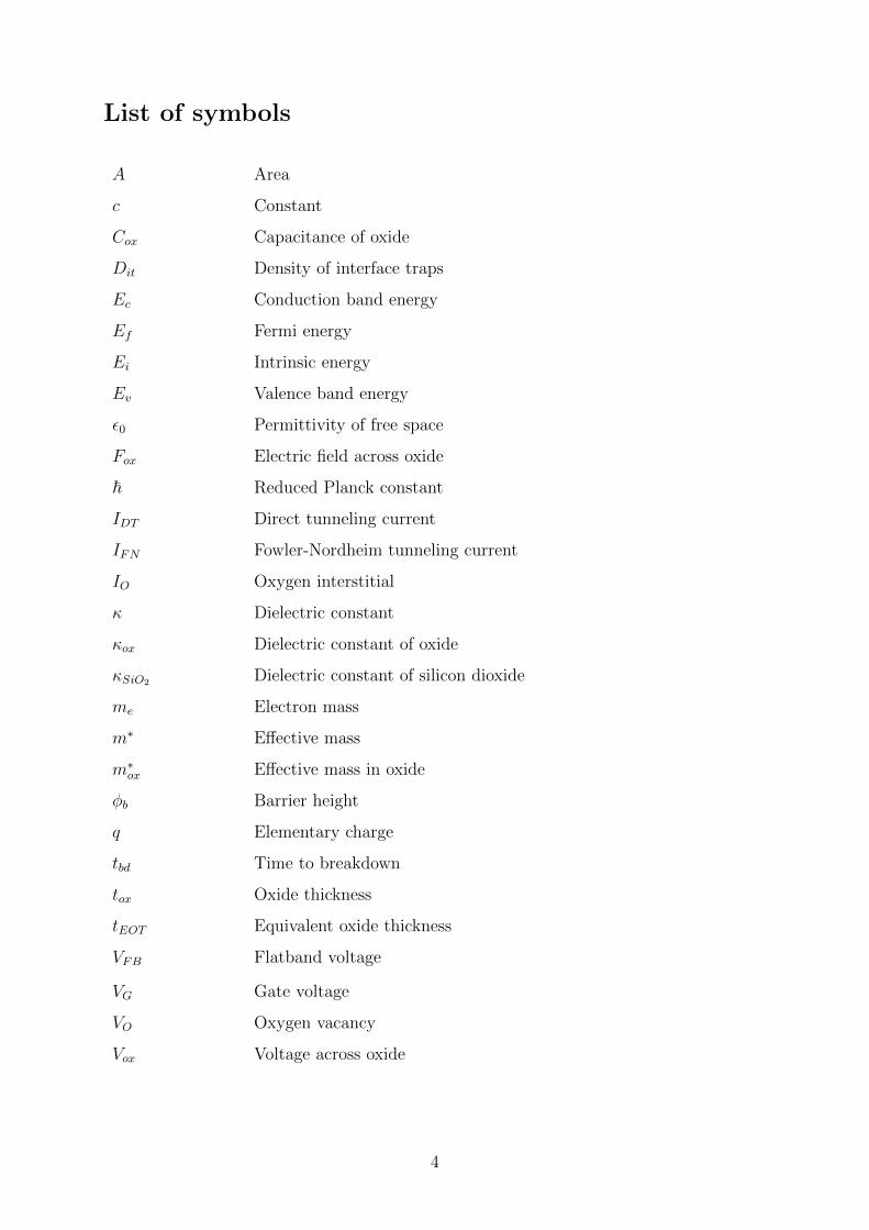
List of symbols
A Area
c Constant
Cox Capacitance of oxide
Dit Density of interface traps
Ec Conduction band energy
Ef Fermi energy
Ei Intrinsic energy
Ev Valence band energy
ε0 Permittivity of free space
Fox Electric field across oxide
~ Reduced Planck constant
IDT Direct tunneling current
IFN Fowler-Nordheim tunneling current
IO Oxygen interstitial
κ Dielectric constant
κox Dielectric constant of oxide
κSiO2 Dielectric constant of silicon dioxide
me Electron mass
m∗ Effective mass
m∗ox Effective mass in oxide
φb Barrier height
q Elementary charge
tbd Time to breakdown
tox Oxide thickness
tEOT Equivalent oxide thickness
VFB Flatband voltage
VG Gate voltage
VO Oxygen vacancy
Vox Voltage across oxide
4
1 Introduction
The first transistor was invented in 1947, and it was perhaps the most important electronicinvention of the century. It allowed the production of integrated circuits and processorsthat are the building stones of modern electronics. The development of transistors tookoff rapidly and in 1965, Gordon E. Moore formulated the famous Moore’s law which statesthat the density of transistors in an integrated circuit will double every two years. Theclaim proves surprisingly accurate even today[1].
A metal oxide semiconductor (MOS) capacitor is the basis for the metal oxide semicon-ductor field effect transistor (MOSFET) which is a common type of transistor. As thename suggests, the MOS and MOSFET are constructed of three layers of a semiconduc-tor, an oxide, and a metal. The MOSFET behaves as a switch with on and off states, andas a result, the switching speed and the switching energy are important properties. Withthe reduction in transistor size, the switching speed has significantly increased while theswitching energy has decreased[2].
Among the many advantages of the downscaling of transistors, there are also disadvan-tages. The dominant semiconductor material throughout history has been silicon (Si)with an oxide layer of silicon dioxide (SiO2), and when the SiO2 layer becomes thinner,the effect of quantum mechanical tunneling increases and gives rise to a gate leakagecurrent. The gate leakage current can result in an unacceptably large current loss thatsignificantly increases power consumption. In addition, high leakage currents reduce thereliability of the oxide layer which raises the risk of an undesired dielectric breakdown[3].
If progress in transistor technology is to continue, the power consumption issue has tobe overcome. One way is to introduce other materials than Si and SiO2 to use for thetransistors. A semiconductor with a lower effective electron mass than Si should have ahigher carrier mobility, and would obtain the same switching speed as Si but at a loweroperating voltage, reducing energy losses. An oxide with a high dielectric constant couldbe built thicker than SiO2 but retain the electrical properties to reduce the leakage cur-rent, and subsequently, the power consumption[2].
Promising candidates to replace Si are group III-V compound materials. The electronmobility of compounds such as indium gallium arsenide (InGaAs) proves higher than formost other known substances[2]. A big advantage that Si has over semiconductors ofthese materials however, is that its native oxide SiO2 is a decent insulator and can beeffortlessly grown on top of the Si layer. The native oxides of group III-V semiconductorsare poor, and more advanced methods are required for the selection and application of adifferent oxide, typically a dielectric material with a high dielectric constant[3].
The aim of this work was to investigate various electrical properties of a MOS deviceconstructed of an InGaAs semiconductor and a hafnium dioxide (HfO2) insulator. Threesamples of varying thicknesses and preparation methods were to be processed and theirbreakdown voltage, time dependent dielectric breakdown (TDDB) and temperature de-pendence of the leakage current measured. The results should then be used to increaseunderstanding of what leakage and breakdown mechanisms are active in the samples.
5
2 Theory
A MOS consists of a semiconductor layer, an oxide layer and a metal layer. The semicon-ductor layer can be n-doped (p-MOS) or p-doped (n-MOS). Above the semiconductor isthe oxide layer which functions as an insulator. At the top is the metal layer, also knownas the gate metal. In this chapter, relevant theory about the MOS capacitor will bediscussed, including choice of materials, energy band structure and leakage mechanisms.
2.1 Material properties
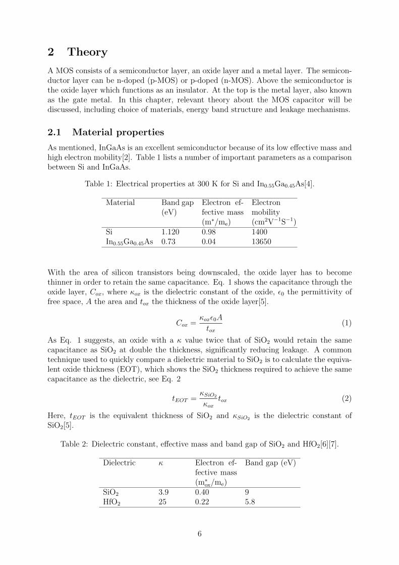
As mentioned, InGaAs is an excellent semiconductor because of its low effective mass andhigh electron mobility[2]. Table 1 lists a number of important parameters as a comparisonbetween Si and InGaAs.
Table 1: Electrical properties at 300 K for Si and In0.55Ga0.45As[4].
Material Band gap(eV)
Electron ef-fective mass(m∗/me)
Electronmobility(cm2V−1S−1)
Si 1.120 0.98 1400In0.55Ga0.45As 0.73 0.04 13650
With the area of silicon transistors being downscaled, the oxide layer has to becomethinner in order to retain the same capacitance. Eq. 1 shows the capacitance through theoxide layer, Cox, where κox is the dielectric constant of the oxide, ε0 the permittivity offree space, A the area and tox the thickness of the oxide layer[5].
Cox =κoxε0A
tox(1)
As Eq. 1 suggests, an oxide with a κ value twice that of SiO2 would retain the samecapacitance as SiO2 at double the thickness, significantly reducing leakage. A commontechnique used to quickly compare a dielectric material to SiO2 is to calculate the equiva-lent oxide thickness (EOT), which shows the SiO2 thickness required to achieve the samecapacitance as the dielectric, see Eq. 2
tEOT =κSiO2
κoxtox (2)
Here, tEOT is the equivalent thickness of SiO2 and κSiO2 is the dielectric constant ofSiO2[5].
Table 2: Dielectric constant, effective mass and band gap of SiO2 and HfO2[6][7].
Dielectric κ Electron ef-fective mass(m∗
ox/me)
Band gap (eV)
SiO2 3.9 0.40 9HfO2 25 0.22 5.8
6
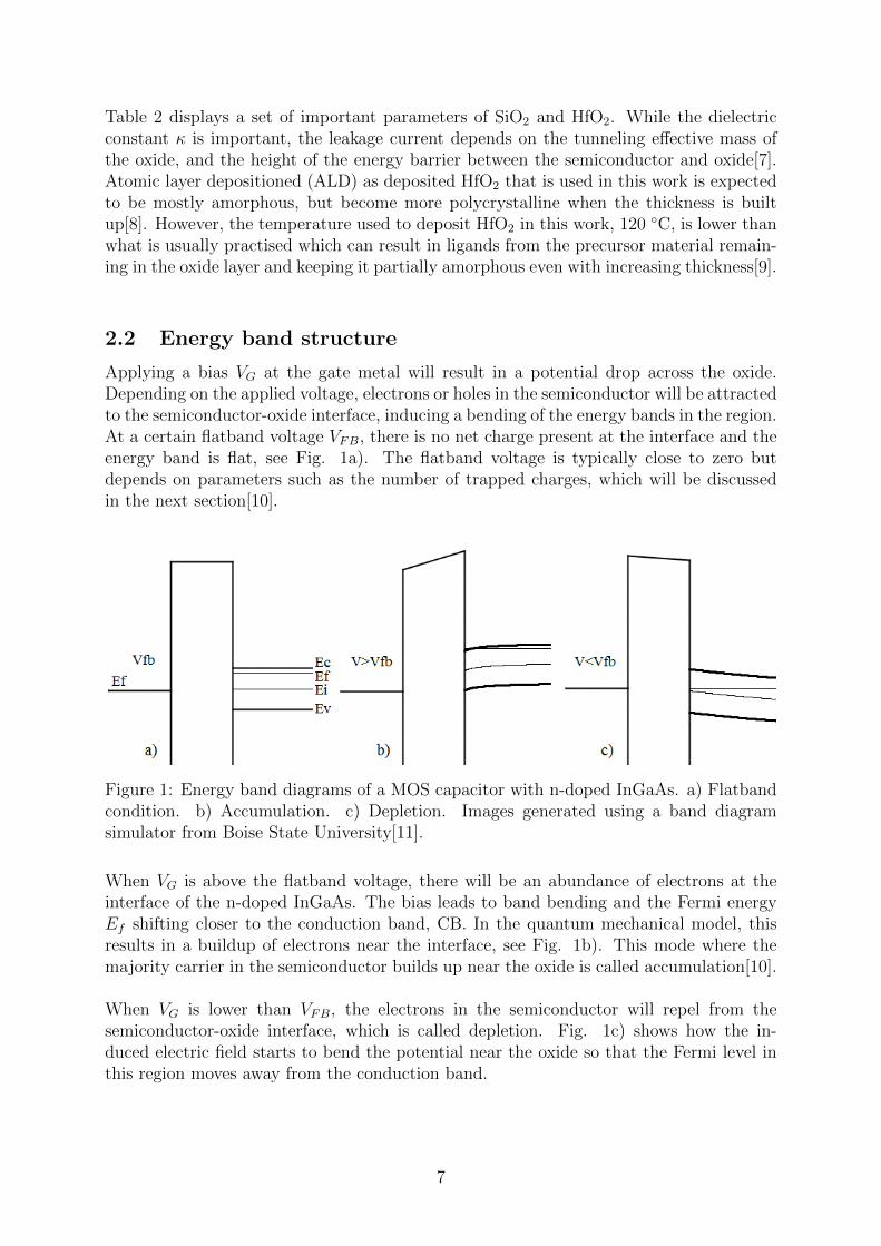
Table 2 displays a set of important parameters of SiO2 and HfO2. While the dielectricconstant κ is important, the leakage current depends on the tunneling effective mass ofthe oxide, and the height of the energy barrier between the semiconductor and oxide[7].Atomic layer depositioned (ALD) as deposited HfO2 that is used in this work is expectedto be mostly amorphous, but become more polycrystalline when the thickness is builtup[8]. However, the temperature used to deposit HfO2 in this work, 120 ◦C, is lower thanwhat is usually practised which can result in ligands from the precursor material remain-ing in the oxide layer and keeping it partially amorphous even with increasing thickness[9].
2.2 Energy band structure
Applying a bias VG at the gate metal will result in a potential drop across the oxide.Depending on the applied voltage, electrons or holes in the semiconductor will be attractedto the semiconductor-oxide interface, inducing a bending of the energy bands in the region.At a certain flatband voltage VFB, there is no net charge present at the interface and theenergy band is flat, see Fig. 1a). The flatband voltage is typically close to zero butdepends on parameters such as the number of trapped charges, which will be discussedin the next section[10].
Figure 1: Energy band diagrams of a MOS capacitor with n-doped InGaAs. a) Flatbandcondition. b) Accumulation. c) Depletion. Images generated using a band diagramsimulator from Boise State University[11].
When VG is above the flatband voltage, there will be an abundance of electrons at theinterface of the n-doped InGaAs. The bias leads to band bending and the Fermi energyEf shifting closer to the conduction band, CB. In the quantum mechanical model, thisresults in a buildup of electrons near the interface, see Fig. 1b). This mode where themajority carrier in the semiconductor builds up near the oxide is called accumulation[10].
When VG is lower than VFB, the electrons in the semiconductor will repel from thesemiconductor-oxide interface, which is called depletion. Fig. 1c) shows how the in-duced electric field starts to bend the potential near the oxide so that the Fermi level inthis region moves away from the conduction band.
7
2.3 Defects
Defects in the oxide layer are sites with an excess or deficit of oxygen atoms, impuritiesof atoms that are not supposed to be in the material, or other types of faulty bonds. Thedefects may be electrically active and create states in the forbidden gap of the oxide thatcan attract electrons or holes from the semiconductor and trap them[12]. The number ofavailable traps depend on applied voltage and the temperature[13].
An advantage of SiO2 over high-κ materials is that the number of intrinsic defects it con-tains is notably lower. One reason for this is the way the silicon atoms bond in the crystal.SiO2 is bound together with covalent bonds of a low coordination. The low coordinationallows the SiO2 crystal to relax and repair any dangling bonds, which is the dominantform of defect. High-κ oxides use ionic bonding with a less adjustable structure[6]. Theirdefects are primarily oxygen vacancies or oxygen deficiencies[14].
The existence of trapped charges in the oxide layer changes the electric field across it.As a result, with zero applied gate voltage, some bending of the potential will already beongoing. It follows that VFB is different from zero as it has to compensate for the trappedcharges in order to obtain a zero field condition at the semiconductor-oxide interface[10].
Defects exist in the bulk of the material but are also created at the semiconductor-oxideinterface where the difference in lattice parameters and bonding structure of the semicon-ductor and oxide may be distinctive[12]. The density of interface traps Dit is importantas the trapping related electric field change is most likely to commence at the interface.There are various surface treatment techniques and deposition methods available thatcan be used to improve the semiconductor-oxide interface, but the result is unlikely tobe ideal. Another way to reduce the amount of defects in a high-κ oxide is by annealingthe MOS capacitor after fabrication, which is typically done by subjecting the sample toa heated gas of N2/H2. The annealing process may remove impurities which compressesthe oxide layer[6]. Annealing can also close off dangling bonds in the oxide through bond-ing with hydrogen from the H2 gas, which further reduces the number of active defects[12].
The defects in the oxide that are most likely to trap charges are those that reside in the en-ergy range of the Fermi level Ef , which generally varies roughly between the valence bandand conduction band edges of the semiconductor. The energy states of defects depend onthe crystallinity of the oxide and in the case of interface traps, on the semiconductor-oxideinterface texture. The energy levels can be measured or calculated theoretically, whichcan be very difficult for amorphous materials where the variation in atomic configurationis large[15].
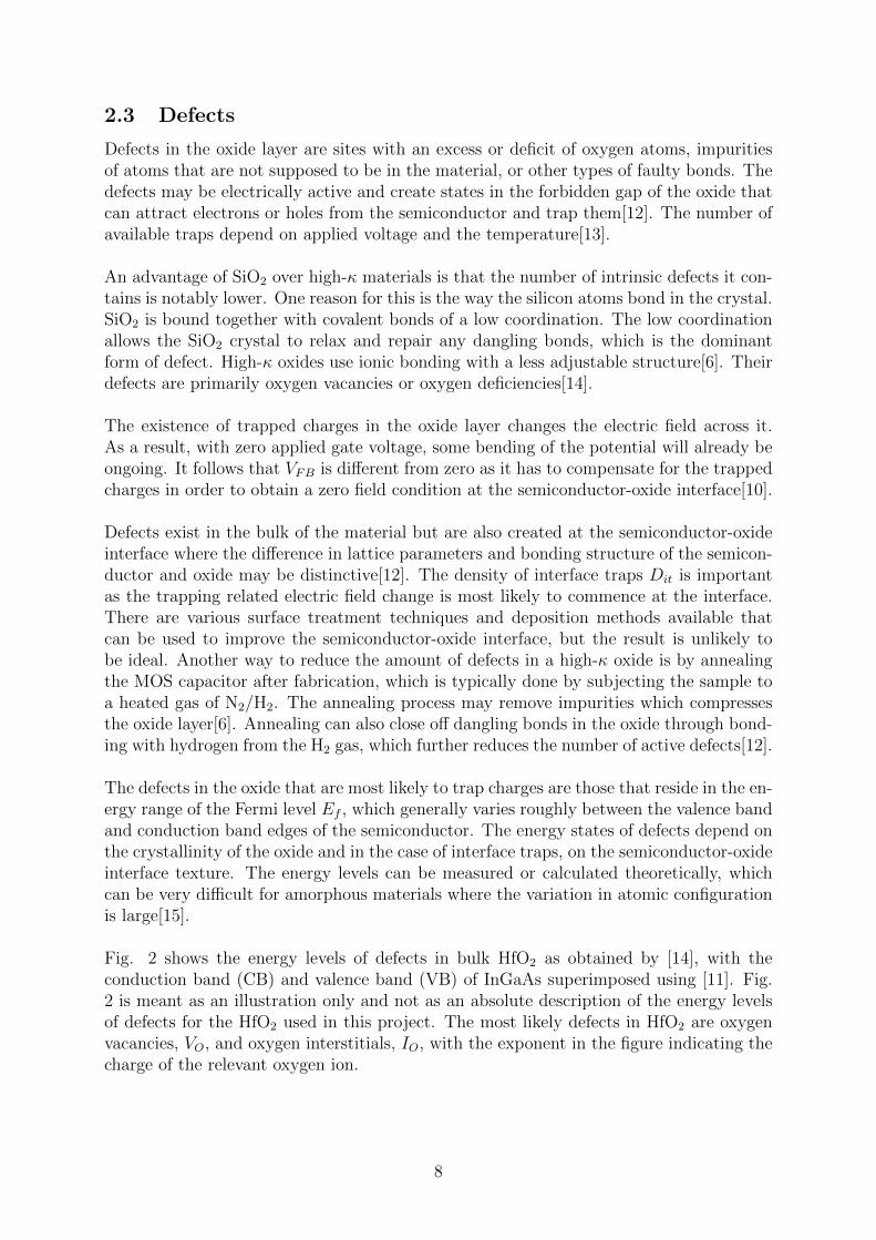
Fig. 2 shows the energy levels of defects in bulk HfO2 as obtained by [14], with theconduction band (CB) and valence band (VB) of InGaAs superimposed using [11]. Fig.2 is meant as an illustration only and not as an absolute description of the energy levelsof defects for the HfO2 used in this project. The most likely defects in HfO2 are oxygenvacancies, VO, and oxygen interstitials, IO, with the exponent in the figure indicating thecharge of the relevant oxygen ion.
8
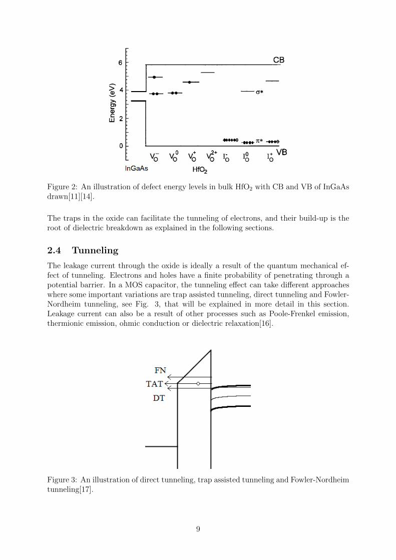
Figure 2: An illustration of defect energy levels in bulk HfO2 with CB and VB of InGaAsdrawn[11][14].
The traps in the oxide can facilitate the tunneling of electrons, and their build-up is theroot of dielectric breakdown as explained in the following sections.
2.4 Tunneling
The leakage current through the oxide is ideally a result of the quantum mechanical ef-fect of tunneling. Electrons and holes have a finite probability of penetrating through apotential barrier. In a MOS capacitor, the tunneling effect can take different approacheswhere some important variations are trap assisted tunneling, direct tunneling and Fowler-Nordheim tunneling, see Fig. 3, that will be explained in more detail in this section.Leakage current can also be a result of other processes such as Poole-Frenkel emission,thermionic emission, ohmic conduction or dielectric relaxation[16].
Figure 3: An illustration of direct tunneling, trap assisted tunneling and Fowler-Nordheimtunneling[17].
9
2.4.1 Trap assisted tunneling
Trap assisted tunneling (TAT) is the effect of carriers tunneling to electrically activedefects in the oxide. As the electric field or temperature increases the probability oftunneling to a trap increases, after which the electron can tunnel further towards thegate metal. If the applied voltage is reduced, trapped charges may detrap back to theoxide. The TAT clearly depends on the density of traps in the oxide and is thereforegenerally more relevant in high-κ materials where the amount of intrinsic defects tend tobe larger[18].
Trap assisted tunneling of electrons is not an elastic process. Electrons that tunnel to adefect release phonons of energy ~ω to reduce their energy to that of the trap. The TATprocess through the oxide has two models. The process may be by single-trap assistedtunneling (STAT), which is a two-step process where the carrier passes through one trapon its way to the oxide, or by multi-trap assisted tunneling (MTAT), where if the oxideis highly degraded with defects, the carrier can hop between multiple traps to permeatethe oxide[12]. An illustration of an STAT process can be seen in Fig. 3.
2.4.2 Direct tunneling
Direct tunneling is only detectable when the oxide thickness is very thin, in the order ofa few nm. Direct tunneling of electrons or holes refers to the penetration of the carrierbetween bands in the semiconductor and gate metal directly through the oxide. The threetypes of tunneling electron tunneling from the conduction band (ECB), electron tunnelingfrom the valence band (EVB) and hole tunneling from the valence band (HVB) are allvariations of direct tunneling through the potential barrier caused by the insulating ox-ide. HVB is effectively the same thing as electron tunneling from valence band to valenceband. An illustration of ECB is shown in Fig. 3[7][17].
Deriving an expression for the direct tunneling is a difficult process that requires numer-ous assumptions. Eq. 3 is a model for the direct tunneling gate current where the finiteavailability of carriers for tunneling is neglected. This result is an acceptable approxima-tion except for very thin oxides (< 2 nm) at low voltages[17].
IDT = c · F 2oxexp
{− 4
3
√2m∗
oxφ3/2b
~q1
Fox
[1− (1− qVox
φb
)3/2]}
(3)
In this expression, c is a constant, Fox is the electric field across the oxide, m∗ox is the
effective electron mass in the oxide, φb is the barrier height between conduction bandsat the semiconductor-oxide interface, ~ is the reduced Planck constant, q is the electroncharge and Vox is the voltage across the oxide. The electric field induced across the oxideis given by
Fox =VGtox
(4)
10
2.4.3 Fowler-Nordheim tunneling
Fowler-Nordheim (FN) tunneling through the oxide can occur when a large enough biasis applied at the gate to shift the side of the potential barrier near the metal downwards.The electrons in the conduction band can tunnel through the then triangular shaped po-tential barrier, see Fig. 3. The triangular shape effectively makes the barrier thinner andthe probability of tunneling higher[19].
By making the assumptions that the available electrons for tunneling can be described asa Fermi gas and their availability is not governed by temperature, and that the potentialbarrier shape is triangular, Eq. 5 can be deduced for the tunneling current caused by theFN effect. If FN tunneling is the dominant leakage mechanism, the logarithm of IFN/F
2ox
against 1/Fox should yield a straight line[17].
IFN = c · F 2oxexp
[− 4
3
√2m∗
oxφ3/2b
~q1
Fox
](5)
2.5 Dielectric breakdown
Under high electrical stress, a large number of traps in the oxide will be filled and theremay even be additional conductive spots generated if the applied bias is sufficiently high.These spots can be seen experimentally using various techniques such as AFM relatedmeasurements[20]. The additional traps filled or created causes an increased leakage cur-rent known as the stress induced leakage current (SILC)[12].
The position of a trap is area independent and it can form anywhere in the oxide. How-ever, experiments show that the grain boundaries between crystallites in the oxide have agreater density of filled traps than other regions. With sufficient degradation of the oxide,a series of traps may be formed along the grain boundaries and create a conduction paththat electrons can hop through from trap to trap, which greatly increases leakage current.The creation of a conduction path is referred to as a dielectric breakdown and the impactof it has two stages, a soft breakdown or a hard breakdown[13].
A soft breakdown is characterised by a large and abrupt increase in leakage current. Thesudden escalation can be explained by a single percolation path being formed which allowsmore electrons to flow through the oxide, see Fig. 4. A hard breakdown is also identi-fied by an abrupt increase in leakage current, but multiple order of magnitudes higherthan in a soft breakdown, see Fig 4b). After a hard breakdown, the oxide is highly dam-aged and its structure destroyed, and it has effectively turned into an ohmic conductor[21].
11
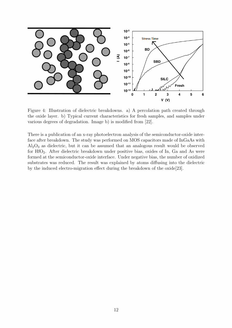
Figure 4: Illustration of dielectric breakdowns. a) A percolation path created throughthe oxide layer. b) Typical current characteristics for fresh samples, and samples undervarious degrees of degradation. Image b) is modified from [22].
There is a publication of an x-ray photoelectron analysis of the semiconductor-oxide inter-face after breakdown. The study was performed on MOS capacitors made of InGaAs withAl2O3 as dielectric, but it can be assumed that an analogous result would be observedfor HfO2. After dielectric breakdown under positive bias, oxides of In, Ga and As wereformed at the semiconductor-oxide interface. Under negative bias, the number of oxidizedsubstrates was reduced. The result was explained by atoms diffusing into the dielectricby the induced electro-migration effect during the breakdown of the oxide[23].
12
3 Experiments
Three MOS samples of InGaAs and HfO2 were fabricated in different ways and their mea-surement results compared. Current-voltage (IV ) measurements were performed wherethe leakage current and breakdown points were measured at a varying voltage. Measure-ments where the samples were exposed to a constant voltage stress (CVS), measurementsof the SILC, and IV measurements of unstressed devices under varying temperature weredone.
3.1 Processing
The metal oxide semiconductor arrangement was processed on the surface of an indiumphosphide (InP) wafer. The InP wafer was doped with iron (Fe) to make it non-conductive.Two samples with InGaAs of the composition In0.55Ga0.45As were created. In both sam-ples, HfO2 of different thicknesses was used as the insulator layer. The metal layer wasproduced of a stack of nickel (Ni), palladium (Pd) and gold (Au). The Ni was adminis-tered first due to its good interface with HfO2, and Au was added as the top layer becauseof its high conductivity. Pd was used as an intermediate to prevent the mobile gold atomsfrom piercing into the oxide, and for its good adhesion with Ni and Au.
3.1.1 Surface preparation
To optimize the interface between the InGaAs and HfO2 layers, the InGaAs surface hadto be thoroughly cleaned and deprived of native oxides. To eliminate undesired particlesfrom the surface, the samples were immersed in acetone and positioned in an ultrasoniccleaner for 3 min. The ultrasonic cleaning process was then repeated twice where acetonewas replaced with isopropanol and distilled water respectively. To clear out native oxides,the samples were placed in a 1:1 hydrochloric (HCl) solution for 30 s and rinsed in water.
One sample underwent an additional process that the other did not. A dummy gate wascreated using a technique similar to how the drain and source would be created in a MOS-FET. The sample was baked on a hot plate at 200 ◦C for 5 min. Hydrogen silsesquioxane(HSQ) was then spin coated onto the surface at 3000 rpm for 1 min, after which thesample was positioned on the 200 ◦C hot plate again for 1 min. The sample was thencured in an oven at 300 ◦C for 60 min.
The cleaning process of the surface continued by the samples being placed in hydrofluoricacid (HF) for 3 min and then rinsed with water, which removed the HSQ applied to one ofthem. Previous experiments show that the dummy gate process has no significant effecton the results of measurements on the sample. After the HF treatment, the samples wereprocessed in an ozone cleaner for 15 min, in which UV radiation is absorbed by oxygen(O2) on the sample that turns into atomic oxygen (O) and ozone (O3). The variousoxygen molecules react with free radicals that were released in the UV process, to formmolecules such as carbon dioxide (CO2) or water vapour (H2O)[24]. Finally, the sampleswere immersed into a solution of (NH4)2S · 20% H2O for 20 min.
13
3.1.2 Atomic Layer Deposition
To administer the HfO2 layer on top of the cleaned InGaAs surfaces, atomic layer depo-sition (ALD) was used. ALD is a method commonly utilized to deposit thin films withprecision in thickness down to monoatomic layers. Such a high level of control is achievedby releasing two precursor substances into the chamber where the sample is located, onefor Hf and one for O, alternating between them. The precursors will attach to everyavailable surface site and if both of them give rise to a self-limiting process where only asingle layer is deposited during each sequence, very high precision is achieved[25]. As aprecursor for Hf, tetrakis(dimethylamido)hafnium (TDMA-Hf) was used and H2O vapouras a precursor for oxygen.
The ALD chamber was first ventilated with N2 for 20 min. It was then heated to 120◦C, and the Hf precursor was heated to 75 ◦C and the temperatures were stabilized for2 min before the process started. The ALD began with five 0.15 s pulses of TDMA-Hf,with 50 s wait time in between, being released into the chamber to achieve a self-cleaningeffect. ALD self-cleaning is a phenomenon where the Hf precursor and native oxides onthe InGaAs surface perform substitution reactions to cleanse the surface of native oxidesand create HfO2[26]. After the initial pulses of TDMA-Hf, 0.15 s pulses of TDMA-Hf and0.015 s pulses of water vapour were alternated, ventilating the chamber with N2 during50 s downtime periods between each pulse. The cycle of varying TDMA-Hf and H2Opulses was repeated 60 times for one sample, and 40 times for the other, where one cycleis expected to roughly correspond to a layer of 1 A, for thicknesses of 6 nm and 4 nm.
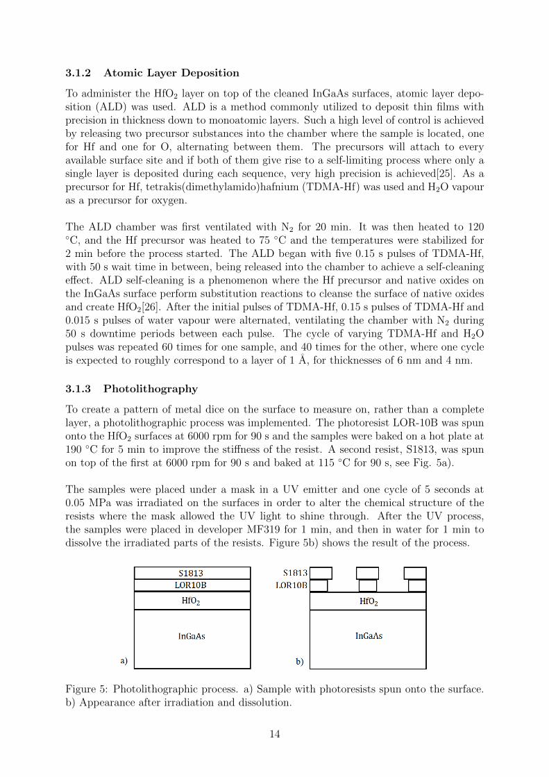
3.1.3 Photolithography
To create a pattern of metal dice on the surface to measure on, rather than a completelayer, a photolithographic process was implemented. The photoresist LOR-10B was spunonto the HfO2 surfaces at 6000 rpm for 90 s and the samples were baked on a hot plate at190 ◦C for 5 min to improve the stiffness of the resist. A second resist, S1813, was spunon top of the first at 6000 rpm for 90 s and baked at 115 ◦C for 90 s, see Fig. 5a).
The samples were placed under a mask in a UV emitter and one cycle of 5 seconds at0.05 MPa was irradiated on the surfaces in order to alter the chemical structure of theresists where the mask allowed the UV light to shine through. After the UV process,the samples were placed in developer MF319 for 1 min, and then in water for 1 min todissolve the irradiated parts of the resists. Figure 5b) shows the result of the process.
Figure 5: Photolithographic process. a) Sample with photoresists spun onto the surface.b) Appearance after irradiation and dissolution.
14
3.1.4 Metallisation
The metallisation was done by placing the sample in an evaporation chamber. The cham-ber was emptied of air after pieces of Ni, Pd and Au were positioned in the chamber. Adetector in the ceiling measured the thicknesses of the metal layers created on the samplesas the evaporated metals cooled down. The detector had a resolution down to the A level.
The metallisation was done on the 6 nm sample first beginning with the evaporation ofNi until a thickness of 4 nm was achieved. Next a 10 nm layer of Pd and finally a 200 nmlayer of gold. The measured layer thicknesses on the 4 nm sample were 6 nm Ni, 11 nmPd and 170 nm Au.
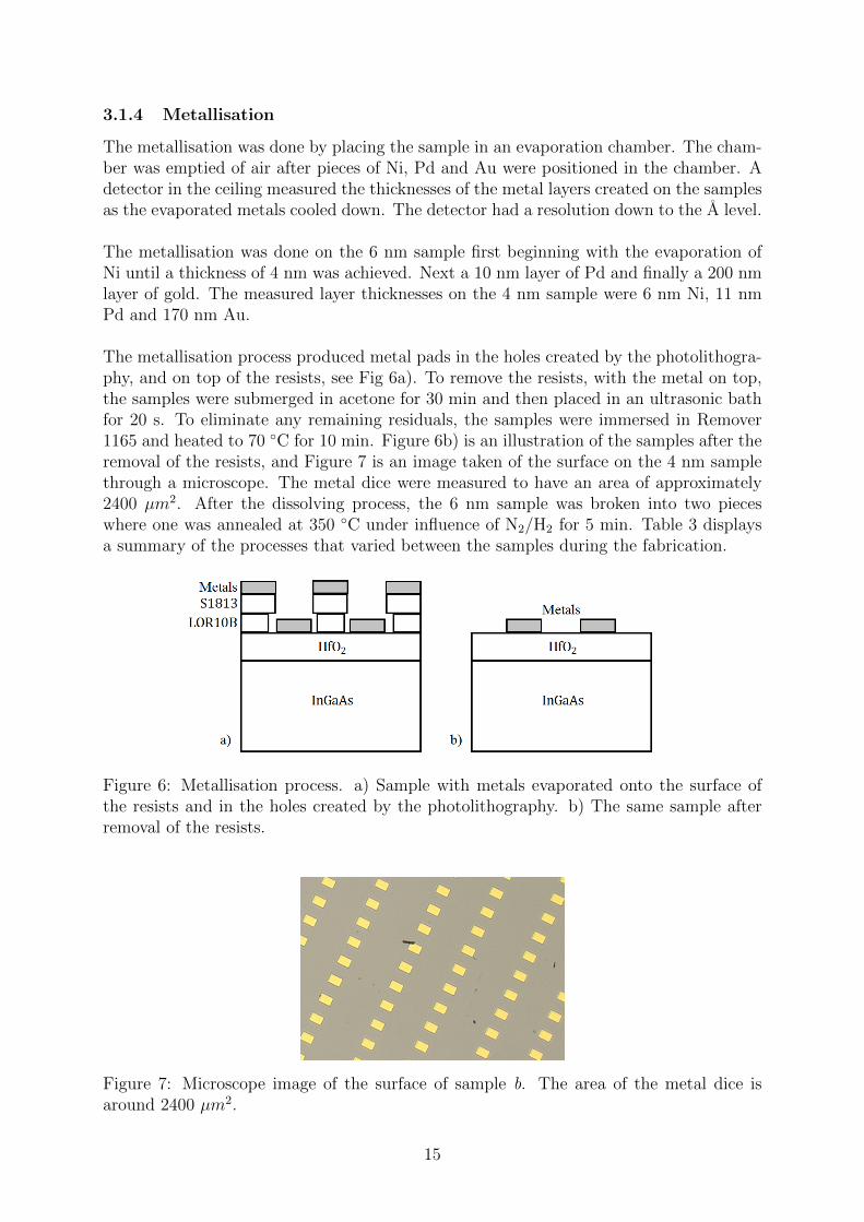
The metallisation process produced metal pads in the holes created by the photolithogra-phy, and on top of the resists, see Fig 6a). To remove the resists, with the metal on top,the samples were submerged in acetone for 30 min and then placed in an ultrasonic bathfor 20 s. To eliminate any remaining residuals, the samples were immersed in Remover1165 and heated to 70 ◦C for 10 min. Figure 6b) is an illustration of the samples after theremoval of the resists, and Figure 7 is an image taken of the surface on the 4 nm samplethrough a microscope. The metal dice were measured to have an area of approximately2400 µm2. After the dissolving process, the 6 nm sample was broken into two pieceswhere one was annealed at 350 ◦C under influence of N2/H2 for 5 min. Table 3 displaysa summary of the processes that varied between the samples during the fabrication.
Figure 6: Metallisation process. a) Sample with metals evaporated onto the surface ofthe resists and in the holes created by the photolithography. b) The same sample afterremoval of the resists.
Figure 7: Microscope image of the surface of sample b. The area of the metal dice isaround 2400 µm2.
15
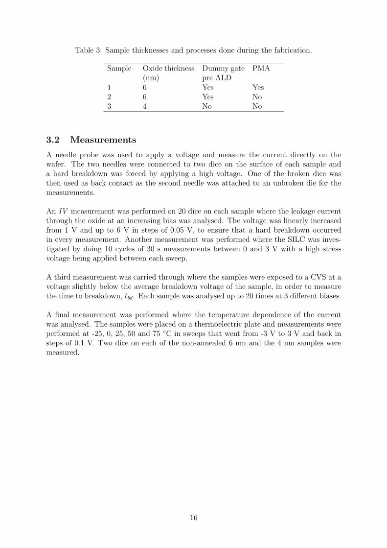
Table 3: Sample thicknesses and processes done during the fabrication.
Sample Oxide thickness(nm)
Dummy gatepre ALD
PMA
1 6 Yes Yes2 6 Yes No3 4 No No
3.2 Measurements
A needle probe was used to apply a voltage and measure the current directly on thewafer. The two needles were connected to two dice on the surface of each sample anda hard breakdown was forced by applying a high voltage. One of the broken dice wasthen used as back contact as the second needle was attached to an unbroken die for themeasurements.
An IV measurement was performed on 20 dice on each sample where the leakage currentthrough the oxide at an increasing bias was analysed. The voltage was linearly increasedfrom 1 V and up to 6 V in steps of 0.05 V, to ensure that a hard breakdown occurredin every measurement. Another measurement was performed where the SILC was inves-tigated by doing 10 cycles of 30 s measurements between 0 and 3 V with a high stressvoltage being applied between each sweep.
A third measurement was carried through where the samples were exposed to a CVS at avoltage slightly below the average breakdown voltage of the sample, in order to measurethe time to breakdown, tbd. Each sample was analysed up to 20 times at 3 different biases.
A final measurement was performed where the temperature dependence of the currentwas analysed. The samples were placed on a thermoelectric plate and measurements wereperformed at -25, 0, 25, 50 and 75 ◦C in sweeps that went from -3 V to 3 V and back insteps of 0.1 V. Two dice on each of the non-annealed 6 nm and the 4 nm samples weremeasured.
16
4 Results and discussion
The breakdown voltage, breakdown time and SILC measurements were performed on allsamples while the temperature dependency was only done on the 6 nm as deposited andthe 4 nm samples. For the sake of consistency, when comparing the outcomes of morethan one sample, the results from the 6 nm as deposited sample are displayed in black,the 6 nm annealed sample in red, and the 4 nm sample in blue.
4.1 Breakdown voltage
Fig. 8a) shows the distribution of the breakdown voltage obtained for the three samples.Fig. 8b) shows a cumulative distribution plot of the breakdowns, plotted against electricfield. The 4 nm sample clearly displays the highest breakdown field, while the annealed6 nm sample appears to be the worst of the three.
Figure 8: Distribution of the breakdown voltage in the three samples. a) A histogramshowing the number of dice that broke within each range of 0.05 V. b) A cumulativedistribution plot of the breakdown points.
For all three samples, the distribution covers a wide bias range which indicates a largevariation in defect density and placement in the oxide. The diversity could stem froma variety of sources. The clean room used for the fabrication belongs to the universitywhere the work is done by hand, and may not be at industrial standards where processesare done automatically without human error and contamination. The samples were ex-posed to air for a period of time between the steps in the cleaning process and before theALD, which could make an important impact on the quality of the InGaAs surface andsemiconductor-oxide interface. Native oxides could have formed during the exposure thatthe ALD self cleaning process did not clear out.
The ALD process was done at the relatively low temperature of 120 ◦C where the amountof defects created should be higher than at temperatures around 300 ◦C. The oxide prop-erties should also be slightly worse, however the oxide should become more crystalline athigher temperature[9].
17
The thin 4 nm sample could withstand a higher electrical field before breaking. Thereason for this could be a lower grade of crystallinity. As the HfO2 layer grows thickerin the ALD process, the layer should become increasingly polycrystalline from the moreamorphous state of the initial layers[8]. The 6 nm samples should therefore have moregrain boundaries than the 4 nm sample. As previously mentioned, the defect paths tendto prefer to follow grain boundaries and the leakage current should then be higher in the6 nm samples than in the 4 nm sample at the same electric field[13].
The 6 nm annealed sample breaks at a lower electric field than the as deposited 6 nm sam-ple. The reason why the annealed sample shows worse properties than the non-annealedcould also be connected to the crystallinity of the samples. The annealing process is sup-posed to reduce the number of defects and may compress the oxide which also tends toalign the crystals in the layer. If the grain boundaries are more aligned in the annealedsample, creating a conduction path through the oxide in the annealed sample should bemore achievable than in the non-annealed sample.
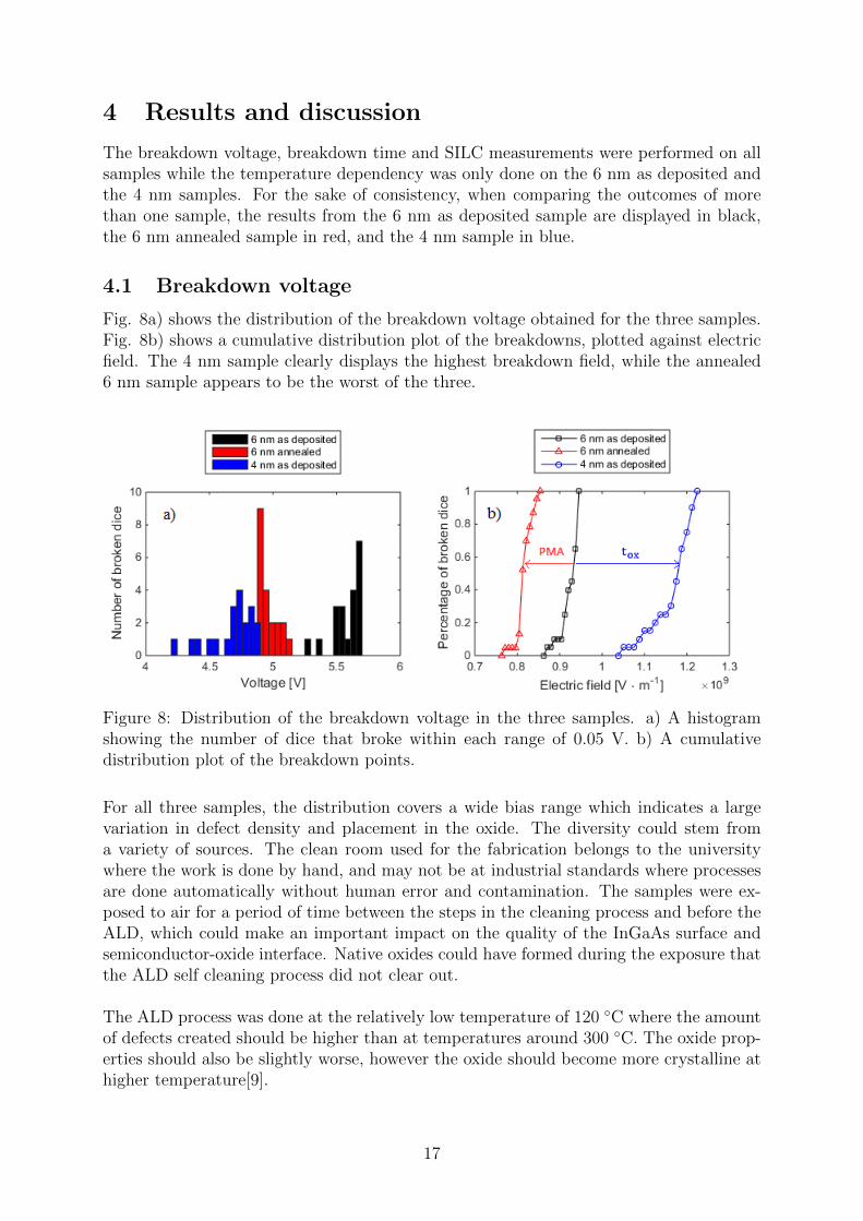
A plot of the leakage current leading up to the breakdown can be seen in Fig. 9. Themeasurement was performed first on the 6 nm annealed sample with a poor resolution atthe lower currents, and these parts are thus chosen not to be displayed in the graph. Thelower resolution also explains the high amount of noise that can be seen in the plot justbefore the breakdown of the annealed sample. To make sure that the leakage current ofthis sample acted in the same way as the other samples, two additional measurementswere performed using the higher resolution. The results of these two measurements canbe observed in the figure to behave in a comparable style at low applied bias.
Figure 9: The leakage current measured at an increasing voltage for the three samples.
In Fig. 9, the measurements of the 4 nm sample appears more noisy than those of the 6nm samples. The reason for the higher noise level is probably a result of the oxide layerbeing thinner, which suggests that the impact each trapped charge has on the leakage
18
current becomes more significant. This effect has been seen before, such as in [27]. As anillustration to allow for easier visualisation, the alignment of two traps in the thin oxidecould allow the electrons to hop through the oxide more easily, while it may require threetraps in a row to cause the same effect in the thicker samples. During the process oftrapping more charges with increasing bias, the thinner sample should therefore see morenoise as the influence of the alignment or disalignment of each electron becoming trappedis more important.
In all samples, the leakage current is observed to increase rapidly between the first mea-surement points when the measurement is begun at 1 V. This is likely a measurementartifact as no such effect was observed in other measurements where the bias range waslarger. After that, the current increases more slowly up until a point around 4 V, de-pending on the sample, where the current begins to rise at a quicker rate. It can beassumed that a different leakage mechanism has become more significant. Finally, thecurrent makes an abrupt increase indicating a hard breakdown. The leakage current inthe 4 nm sample is higher than in the 6 nm samples which is consistent with tunnelingequations like Eq. 4 in which at a constant bias, Fox is higher if the oxide is thin.
A soft breakdown can be distinguished in some of the measurements but most progressdirectly from a low leakage current to a hard breakdown. A soft breakdown was onlyobserved in roughly one tenth of the measurements. The low amount of soft breakdownsdetected is likely a result of the area of the dice measured on being relatively large com-pared to other transistor devices. It has been shown that with a larger area the probabilityof a soft breakdown occurring is reduced[21].
The results from the SILC measurements have been opted not to be shown as they werenot as fruitful as expected. The average measurement showed no clear signs of SILC.What could be construed from the results however was that they coincide with the resultsalready discussed here, such as a soft breakdown only appearing in a small part of themeasurements.
A band diagram simulation was performed in the program from Boise State University[11] where the band structure for different regions of the leakage current graph was inves-tigated. In Fig. 10a) the band structure of the 6 nm sample at 2 V is shown, which is theregion where the current is slowly increasing, and Fig. 10b) shows the band structure at4.5 V which is the region where the current increases at a higher rate.
19
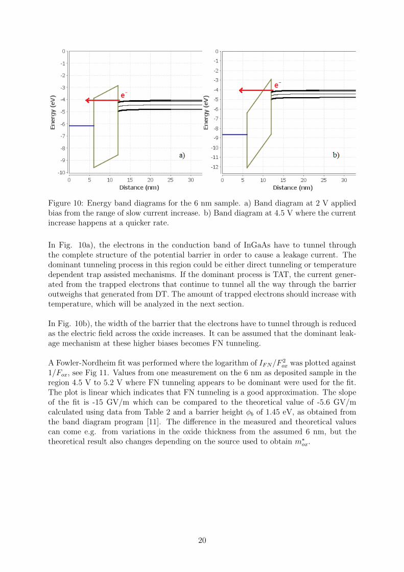
Figure 10: Energy band diagrams for the 6 nm sample. a) Band diagram at 2 V appliedbias from the range of slow current increase. b) Band diagram at 4.5 V where the currentincrease happens at a quicker rate.
In Fig. 10a), the electrons in the conduction band of InGaAs have to tunnel throughthe complete structure of the potential barrier in order to cause a leakage current. Thedominant tunneling process in this region could be either direct tunneling or temperaturedependent trap assisted mechanisms. If the dominant process is TAT, the current gener-ated from the trapped electrons that continue to tunnel all the way through the barrieroutweighs that generated from DT. The amount of trapped electrons should increase withtemperature, which will be analyzed in the next section.
In Fig. 10b), the width of the barrier that the electrons have to tunnel through is reducedas the electric field across the oxide increases. It can be assumed that the dominant leak-age mechanism at these higher biases becomes FN tunneling.
A Fowler-Nordheim fit was performed where the logarithm of IFN/F2ox was plotted against
1/Fox, see Fig 11. Values from one measurement on the 6 nm as deposited sample in theregion 4.5 V to 5.2 V where FN tunneling appears to be dominant were used for the fit.The plot is linear which indicates that FN tunneling is a good approximation. The slopeof the fit is -15 GV/m which can be compared to the theoretical value of -5.6 GV/mcalculated using data from Table 2 and a barrier height φb of 1.45 eV, as obtained fromthe band diagram program [11]. The difference in the measured and theoretical valuescan come e.g. from variations in the oxide thickness from the assumed 6 nm, but thetheoretical result also changes depending on the source used to obtain m∗
ox.
20
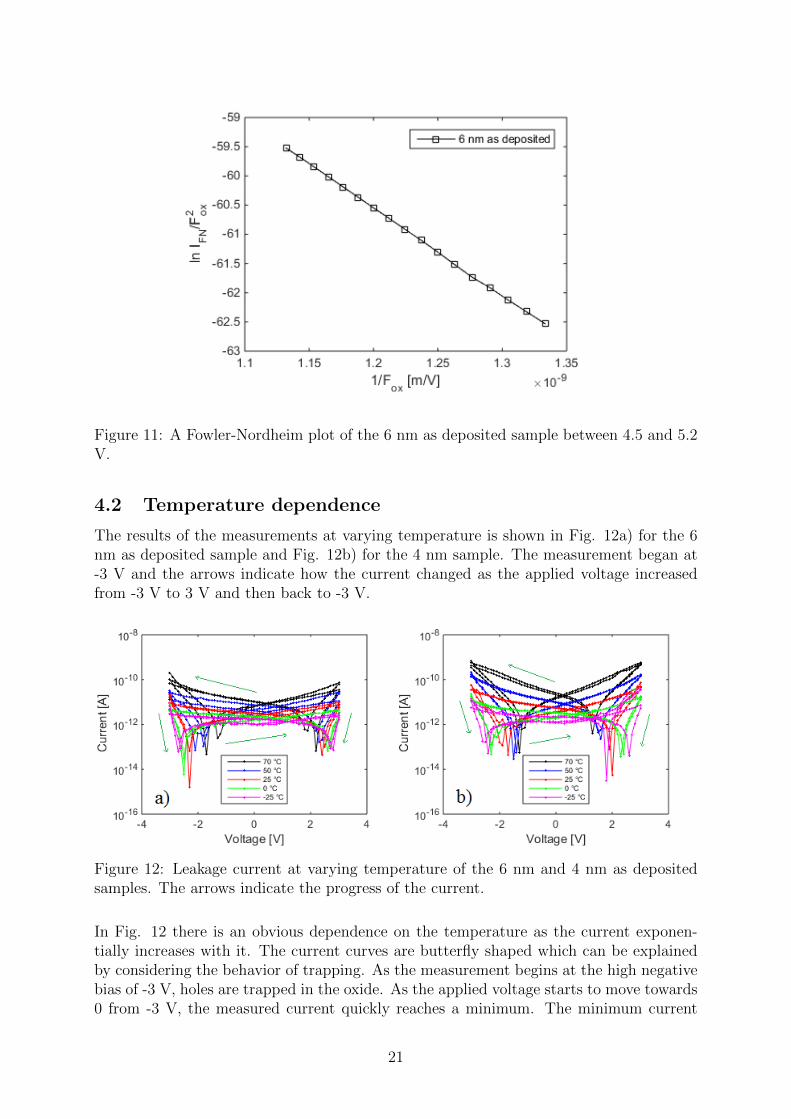
Figure 11: A Fowler-Nordheim plot of the 6 nm as deposited sample between 4.5 and 5.2V.
4.2 Temperature dependence
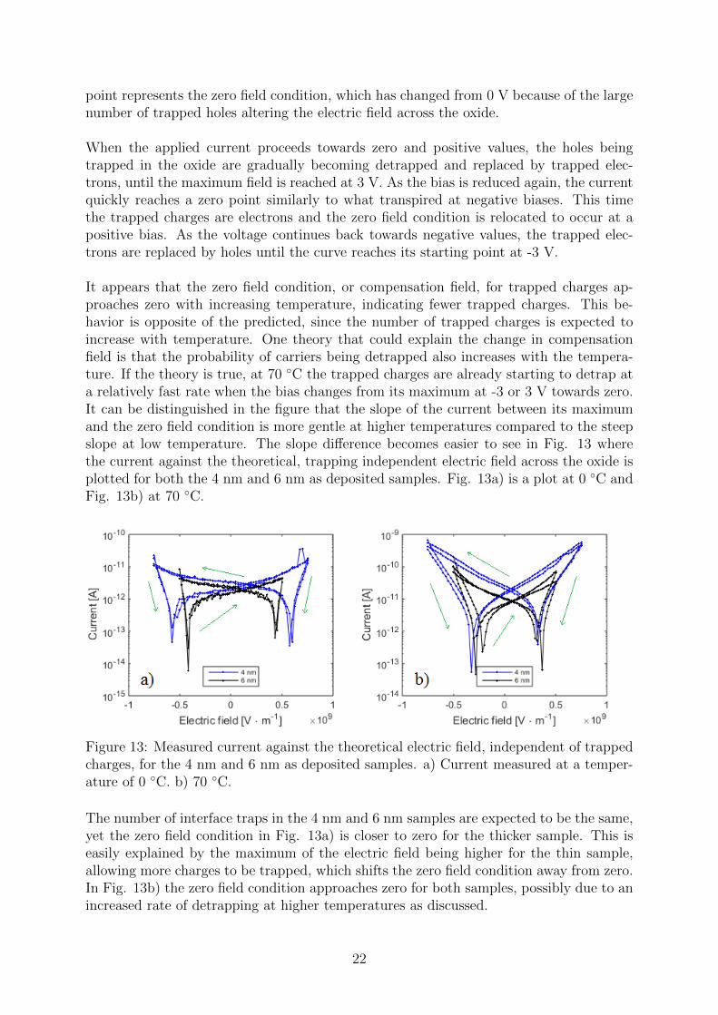
The results of the measurements at varying temperature is shown in Fig. 12a) for the 6nm as deposited sample and Fig. 12b) for the 4 nm sample. The measurement began at-3 V and the arrows indicate how the current changed as the applied voltage increasedfrom -3 V to 3 V and then back to -3 V.
Figure 12: Leakage current at varying temperature of the 6 nm and 4 nm as depositedsamples. The arrows indicate the progress of the current.
In Fig. 12 there is an obvious dependence on the temperature as the current exponen-tially increases with it. The current curves are butterfly shaped which can be explainedby considering the behavior of trapping. As the measurement begins at the high negativebias of -3 V, holes are trapped in the oxide. As the applied voltage starts to move towards0 from -3 V, the measured current quickly reaches a minimum. The minimum current
21
point represents the zero field condition, which has changed from 0 V because of the largenumber of trapped holes altering the electric field across the oxide.
When the applied current proceeds towards zero and positive values, the holes beingtrapped in the oxide are gradually becoming detrapped and replaced by trapped elec-trons, until the maximum field is reached at 3 V. As the bias is reduced again, the currentquickly reaches a zero point similarly to what transpired at negative biases. This timethe trapped charges are electrons and the zero field condition is relocated to occur at apositive bias. As the voltage continues back towards negative values, the trapped elec-trons are replaced by holes until the curve reaches its starting point at -3 V.
It appears that the zero field condition, or compensation field, for trapped charges ap-proaches zero with increasing temperature, indicating fewer trapped charges. This be-havior is opposite of the predicted, since the number of trapped charges is expected toincrease with temperature. One theory that could explain the change in compensationfield is that the probability of carriers being detrapped also increases with the tempera-ture. If the theory is true, at 70 ◦C the trapped charges are already starting to detrap ata relatively fast rate when the bias changes from its maximum at -3 or 3 V towards zero.It can be distinguished in the figure that the slope of the current between its maximumand the zero field condition is more gentle at higher temperatures compared to the steepslope at low temperature. The slope difference becomes easier to see in Fig. 13 wherethe current against the theoretical, trapping independent electric field across the oxide isplotted for both the 4 nm and 6 nm as deposited samples. Fig. 13a) is a plot at 0 ◦C andFig. 13b) at 70 ◦C.
Figure 13: Measured current against the theoretical electric field, independent of trappedcharges, for the 4 nm and 6 nm as deposited samples. a) Current measured at a temper-ature of 0 ◦C. b) 70 ◦C.
The number of interface traps in the 4 nm and 6 nm samples are expected to be the same,yet the zero field condition in Fig. 13a) is closer to zero for the thicker sample. This iseasily explained by the maximum of the electric field being higher for the thin sample,allowing more charges to be trapped, which shifts the zero field condition away from zero.In Fig. 13b) the zero field condition approaches zero for both samples, possibly due to anincreased rate of detrapping at higher temperatures as discussed.
22
It appears that the hysteresis between the two samples in Fig. 13 increases with thetemperature. A reason for this could be that the carriers have a greater energy at highertemperatures which allows them penetrate deeper into the oxide than at low temperature.As a result of the thickness difference, the probability to tunnel through the 4 nm sampleincreases more with the higher energy than through the 6 nm sample, which would ulti-mately lead to more leakage.
4.3 Time dependent dielectric breakdown (TDDB)
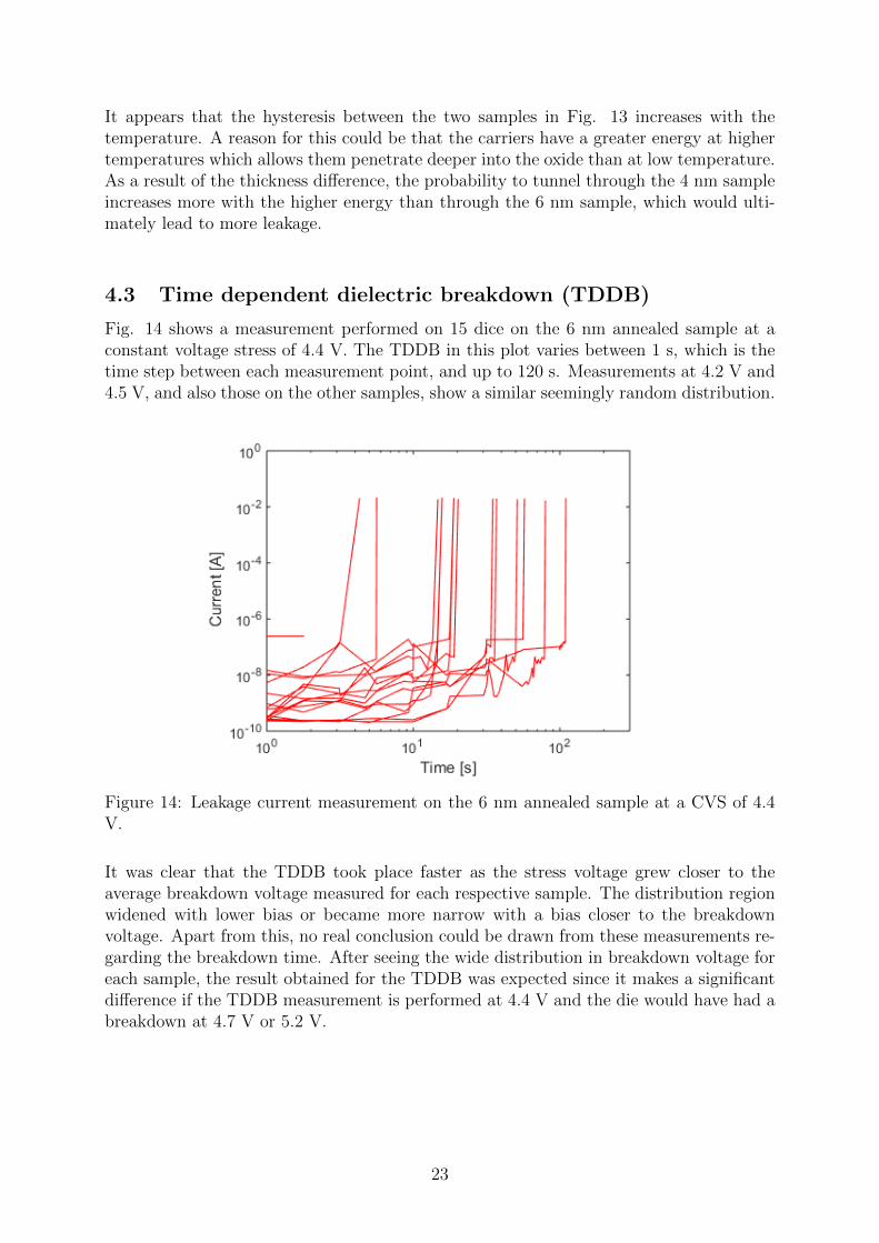
Fig. 14 shows a measurement performed on 15 dice on the 6 nm annealed sample at aconstant voltage stress of 4.4 V. The TDDB in this plot varies between 1 s, which is thetime step between each measurement point, and up to 120 s. Measurements at 4.2 V and4.5 V, and also those on the other samples, show a similar seemingly random distribution.
Figure 14: Leakage current measurement on the 6 nm annealed sample at a CVS of 4.4V.
It was clear that the TDDB took place faster as the stress voltage grew closer to theaverage breakdown voltage measured for each respective sample. The distribution regionwidened with lower bias or became more narrow with a bias closer to the breakdownvoltage. Apart from this, no real conclusion could be drawn from these measurements re-garding the breakdown time. After seeing the wide distribution in breakdown voltage foreach sample, the result obtained for the TDDB was expected since it makes a significantdifference if the TDDB measurement is performed at 4.4 V and the die would have had abreakdown at 4.7 V or 5.2 V.
23
5 Summary and outlook
Three MOS samples using InGaAs with HfO2 layers of 4 nm, 6 nm and 6 nm, applied byALD, were processed. One of the 6 nm samples was annealed. The electric field requiredto cause a hard breakdown through the oxide was ∼ 0.81 GV/m in the 6 nm annealedsample, ∼ 0.90 GV/m in the 6 nm as deposited sample and ∼ 1.13 GV/m in the 4 nmsample and thus it decreased with oxide thickness and PMA treatment. The lower break-down field might be attributed to higher polycrystallinity in the thicker oxides that allowa percolation path to form more easily. The results from all three samples were widelydistributed which likely stemmed from a variation in the density of interface traps acrossthe oxide layer.
The dominant leakage mechanism at higher biases was determined to be Fowler-Nordheimtunneling. The results suggested that direct tunneling or trap assisted tunneling had thelargest influence at low bias, with trap assisted tunneling gaining more significance astemperature increased.
The results obtained in this work could likely have been improved if the fabrication pro-cess was more tightly controlled. With a more uniform oxide layer having fewer defectsdistributed across it directly after the ALD process, the results should have been morecentralized. Besides improving the process utilized in this work, there are numerous otherparameters during the ALD process that can be modified in attempts to improve results,such as changing the temperature and pulse lengths.
The Hf precursor used, TDMA, is a common Hf precursor but there are many othercompounds that include Hf and can be adopted in the ALD process. There could be avariation in how uniformly different precursors administer the Hf across the surface, andhow much contamination of other particles from the precursor end up on the surface.There are also other precursors for oxygen available that can be tested. In addition,methods to reduce the amount of abundant oxygen such as plasma etching are available.Obviously, if interest is not of the results from HfO2/InGaAs in particular, there are manyother materials such as InAs or GaAs as semiconductor, and Al2O3 or ZrO2 as oxide thatcan be used in various combinations.
The measurements suggested that the leakage current increase due to temperature islikely a result of TAT, but other mechanisms can not be discarded. Measurements ofe.g. the relaxation current could have been performed had there been enough time, tounderstand its impact on the leakage current. On the subject of other measurements, CVmeasurements could have been done to identify the filling and creation of interface traps,and XPS measurements could have given an image of the oxide layer in the samples foran assessment of the amount of defects present.
24
Bibliography
[1] Robert R Schaller. Moore’s law: past, present and future. Spectrum, IEEE, 34(6):52–59, 1997.
[2] Jesus A Del Alamo. Nanometre-scale electronics with III-V compound semiconduc-tors. Nature, 479(7373):317–323, 2011.
[3] John Robertson. High dielectric constant gate oxides for metal oxide Si transistors.Reports on Progress in Physics, 69(2):327, 2006.
[4] Ioffe Physico-Technical Institute Website NSM Archive. [Online]. Available at:http://www.ioffe.rssi.ru/SVA/NSM/Semicond/. Acessed 2015-03.
[5] Chris Beer. Fabrication and characterisation of novel Ge MOSFETs. PhD thesis,University of Warwick, 2007.
[6] J Robertson. High dielectric constant oxides. The European physical journal appliedphysics, 28(03):265–291, 2004.
[7] Yee-Chia Yeo, Tsu-Jae King, and Chenming Hu. MOSFET gate leakage modelingand selection guide for alternative gate dielectrics based on leakage considerations.Electron Devices, IEEE Transactions on, 50(4):1027–1035, 2003.
[8] Patrick S Lysaght, Joseph C Woicik, M Alper Sahiner, Byoung-Hun Lee, and RajJammy. Characterizing crystalline polymorph transitions in HfO 2 by extended x-ray absorption fine-structure spectroscopy. Applied Physics Letters, 91(12):122910–122910, 2007.
[9] Claudia Richter, Tony Schenk, Uwe Schroeder, and Thomas Mikolajick. Film prop-erties of low temperature HfO2 grown with H2O, O3, or remote O2-plasma. Journalof Vacuum Science & Technology A, 32(1):01A117, 2014.
[10] Bart Van Zeghbroeck. Principles of semiconductor devices. Colarado University,2004.
[11] Boise State University Band Diagram Program Website. [Online]. Avail-able at: http://nano.boisestate.edu/research-areas/multi-dielectric-energy-band-diagram-program/. Accessed 2015-04.
[12] Robert Entner. Modeling and simulation of negative bias temperature instability.2007, PhD thesis.
[13] G Bersuker, J Yum, L Vandelli, A Padovani, L Larcher, V Iglesias, M Porti, M Nafria,K McKenna, A Shluger, et al. Grain boundary-driven leakage path formation in HfO2dielectrics. Solid-State Electronics, 65:146–150, 2011.
[14] K Xiong, J Robertson, MC Gibson, and SJ Clark. Defect energy levels in HfO 2high-dielectric-constant gate oxide. Applied Physics Letters, 87(18):183505–183505,2005.
[15] JR Weber, A Janotti, and CG Van de Walle. Native defects in Al2O3 and theirimpact on III-V/Al2O3 metal-oxide-semiconductor-based devices. Journal of AppliedPhysics, 109(3):033715, 2011.
25
[16] Simon M Sze and Kwok K Ng. Physics of semiconductor devices. John Wiley &Sons, 2006.
[17] Juan C Ranuarez, M Jamal Deen, and Chih-Hung Chen. A review of gate tunnelingcurrent in MOS devices. Microelectronics reliability, 46(12):1939–1956, 2006.
[18] Michel Houssa, M Tuominen, M Naili, Valeri Afanasev, Andre Stesmans, S Haukka,and MM Heyns. Trap-assisted tunneling in high permittivity gate dielectric stacks.Journal of Applied Physics, 87(12):8615–8620, 2000.
[19] M Lenzlinger and EH Snow. Fowler-Nordheim Tunneling into Thermally GrownSiO2. Journal of Applied physics, 40(1):278–283, 1969.
[20] M Porti, S Gerardin, M Nafrı, X Aymerich, A Cester, A Paccagnella, P Schiavuta,R Pierobon, et al. Systematic characterization of soft-and hard-breakdown spotsusing techniques with nanometer resolution. Microelectronic engineering, 84(9):1956–1959, 2007.
[21] Muhammad A Alam, Bonnie Weir, Jeff Bude, P Silverman, and Don Monroe. Expla-nation of soft and hard breakdown and its consequences for area scaling. In ElectronDevices Meeting, 1999. IEDM’99. Technical Digest. International, pages 449–452.IEEE, 1999.
[22] TP Chen, MS Tse, CQ Sun, S Fung, and KF Lo. Snapback behaviour and itssimilarity to the switching behaviour in ultra-thin silicon dioxide films after hardbreakdown. Journal of Physics D: Applied Physics, 34(17):L95, 2001.
[23] P Shekhter, F Palumbo, K Cohen Weinfeld, and M Eizenberg. X ray photoelectronanalysis of oxide-semiconductor interface after breakdown in Al2O3/InGaAs stacks.Applied Physics Letters, 105(10):102908, 2014.
[24] John R Vig. UV/ozone cleaning of surfaces. Journal of Vacuum Science & TechnologyA, 3(3):1027–1034, 1985.
[25] Steven M George. Atomic layer deposition: An overview. Chemical Reviews,110(1):111–131, 2009.
[26] CH Chang, Y-K Chiou, YC Chang, KY Lee, TD Lin, TB Wu, M Hong, and J Kwo.Interfacial self-cleaning in atomic layer deposition of HfO 2 gate dielectric on In 0.15Ga 0.85 As. Applied physics letters, 89(24):242911–242911, 2006.
[27] N Wrachien, A Cester, E Zanoni, G Meneghesso, YQ Wu, and PD Ye. Degrada-tion of III–V inversion-type enhancement-mode MOSFETs. In Reliability PhysicsSymposium (IRPS), 2010 IEEE International, pages 536–542. IEEE, 2010.
26