Embed Size (px)
Citation preview

Microprocessor-based System DesignRicardo Gutierrez-OsunaWright State University
1
Lecture 15: Memory and I/O interface
g Address spaceg Memory organizationg Asynchronous data transfers
n Read and Write cycles
n DTACK* generation
g Synchronous data transfersg Direct Memory Accessg System control signals

Microprocessor-based System DesignRicardo Gutierrez-OsunaWright State University
2
Address space
g The address bus of the 68000 consists of 23 independent address lines A0-A23
n Since the data bus is 16-bit wide, we have an address space of 8M words
g Two additional control lines are used to select individual bytes
n Upper Data Strobe (UDS*)n Lower Data Strobe (LDS*)
g UDS* and LDS* are used to enable byte-wide upper and lower data banks
n Upper data banks are selected by UDS* and contain data bits D8-D15
n Lower data banks are selected by LDS* and contain data bits D0-D7
g A01-A23 are shared by the two data banks and are used to address individual bytes within each bank
g This physical organization of memory explains why words must be stored at even memory addresses

Microprocessor-based System DesignRicardo Gutierrez-OsunaWright State University
3
Memory organization
g Dedicated and general use memoryn Memory locations 000000 to 0003FE have a dedicated function:
g storage of the interrupt vector table
n The rest of the memory space is for general use, it can be used to store data, instructions or address information
g Three additional output pins on the 68000, the function code (FC0-FC2), indicate whether the bus cycle isn accessing data or program instructionsn being executed in user or supervisor mode
Function codeFC2 FC1 FC0
Reference class
0 0 0 (Unassigned)0 0 1 User data0 1 0 User program0 1 1 (Unassigned)1 0 0 (Unassigned)1 0 1 Supervisor data1 1 0 Supervisor program1 1 1 Interrupt Acknowledge
Exception vector table
General use memory
00000016
0003FE1600040016
FFFFFE16
g By using (FC0-FC2), the memory space can be further divided inton User program segmentn User data segmentn Supervisor program segmentn Supervisor data segment
g As an example, (FC0-FC2) are decoded and used to assert the appropriate chip select (CS*) signals
Microprocessor-based System DesignRicardo Gutierrez-OsunaWright State University
4
Asynchronous memory and I/O interface
g Asynchronous means that n once a bus cycle is initiated to read or write
instructions or data, it is not completed until a response is provided by the memory or I/O subsystem
n This response is an acknowledgement signal that tells the 68000 that the current bus cycle is compete
g The basic asynchronous operation isn The 68000 puts an address on the address bus
and asserts Address Strobe (AS*) to signal memory and I/O devices that a valid address information is available on the bus
n The memory or I/O device asserts Data Transfer Acknowledge (DTACK*) to signal the 68000 that
g valid data is available on the data bus during a read operation (the 68000 latches data when DTACK* is asserted)
g data has been successfully written to the memory or I/O device
g Asynchronous operation allows the 68000 to interface with slow memories or I/O devices

Microprocessor-based System DesignRicardo Gutierrez-OsunaWright State University
5
READ cycle flowchart
g An asynchronous read cycle is characterized by the interlocked handshaking procedure that takes place between
n the bus master (CPU) andn the bus slave (memory or I/O device)
g The following steps take placen The CPU indicates its intentions by
g forcing R/W* HIGH andg setting up an addressg asserting AS*, UDS* and LDS*
n The slave detects that AS*, UDS* and LDS* are asserted and then
g places data on the data busg asserts DTACK*
n Upon DTACK* assertion, the CPUg latches data from data busg Negates AS*, UDS* and LDS*
n Upon negation of AS*, UDS* and LDS*, the slave
g removes data from data busg Negates DTACK*
n At this point we can start a new bus cycle
Address the slave
1. Set R/W* to read2. Place function code on FC0-FC2
3. Place address on A01-A23
4. Assert address strobe AS*5. Assert UDS* and LDS*
Output the data
1. Decode the address2. Place data on D0-D15
3. Assert DTACK*
Acquire the data
1. Latch data2. Negate UDS* and LDS*3. Negate address strobe AS*
Terminate the cycle
1. Remove data from D0-D15
2. Negate DTACK*
Start the next cycle
Bus master Bus slave
Microprocessor-based System DesignRicardo Gutierrez-OsunaWright State University
6
READ cycle timing diagram
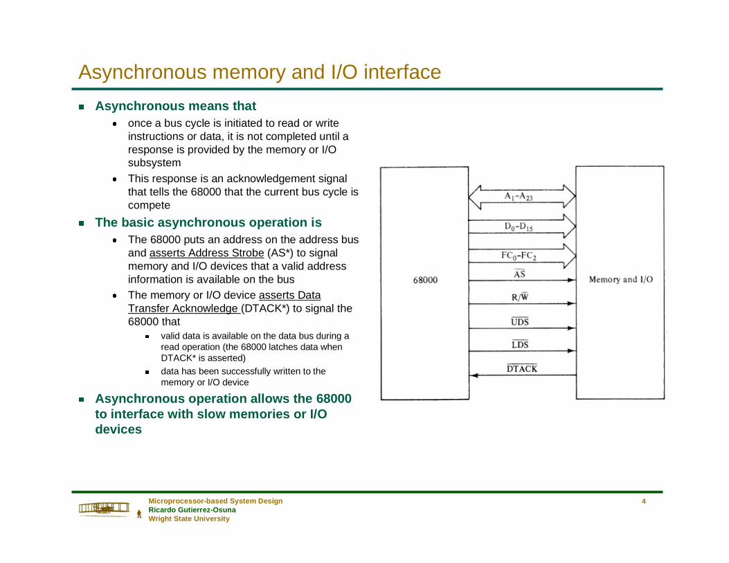
g Each bus cycle consists of a minimum of 4 clock cycles, divided into eight states S0-S7
n A bus cycle starts in state S0 with the clock high and ends in state S7 with the clock low
n This basic cycle can be extended by the insertion of wait states between S4 and S5
g Narrativen During S0 all signals are negated with the
exception of R/W*, which becomes high to indicate a read operation
n In state S1, the address on A01-A23 becomes valid and remains so until state S0 of next cycle
n In state S2 the address strobe AS* goes active-low, indicating that the contents of the address bus are valid
n At the same time, UDS* and LDS* go active-low and initiate the memory access
n At the end of S4, the CPU tests DTACK*g If DTACK* is inactive, the CPU inserts wait
states between S4 and S5 until DTACK* goes active-low on the falling edge of S4
n During S7, the CPU g negates AS*, UDS* and LDS*g latches the data internally
n The negation of the 3 strobes causes the memory to
g return its data output pins to high impedance (floating) state
g negate DTACK*

Microprocessor-based System DesignRicardo Gutierrez-OsunaWright State University
7
WRITE cycle flowchart
g The asynchronous write cycle is very similar to the read cycle we saw before
g There are two differencesn The CPU provides data at the start of the write
cyclen The bus slave reads this data
Address the slave
Input the data
1. Decode address A01-A23
2. Store data from D00-D15
3. Assert DTACK*
Acquire the data
1. Negate UDS* and LDS* 2. Negate address strobe AS* 3. Remove data from D00-D154. Set R/W* to read
Terminate the cycle
1. Negate DTACK*
Start the next cycle
Bus master Bus slave
1. Place function code on FC0-FC2
2. Place address on A01-A23
3. Assert address strobe AS* 4. Set R/W* to write5. Place data on D00-D15
6. Assert UDS* and LDS*

Microprocessor-based System DesignRicardo Gutierrez-OsunaWright State University
8
WRITE cycle timing diagram
g Narrativen At the start of a cycle, an address is
placed on the address bus A01-A23 and g AS* is asserted and R/W* set to logic 0
n After R/W* has set low to indicate a write cycle, the CPU places data on the data bus
n Once the contents of the data bus have stabilized, UDS* and LDS* are asserted (approximately 1 cycle after AS* assertion)
g This allows the memory to use UDS* and LDS* to latch data from the bus
n If DTACK* is asserted before the falling edge of S4, the write cycle is terminated normally
g Otherwise wait states are inserted until DTACK* is asserted
n At the end of the write cycleg AS*, UDS* and LDS* are negated
simultaneouslyg R/W* is set highg data bus is floated

Microprocessor-based System DesignRicardo Gutierrez-OsunaWright State University
9
DTACK* generation
g In the previous slides we assumed that DTACK* was generated by the memory blockn This is true for I/O devices such as the 68230 PI/T or the 68681 DUART, which support asynchronous data
transfers and have a DTACK* output pinn For devices that do not have this facility (such as memory ICs), the DTACK* signal must be generated by
the systems designer with additional circuitry
g The circuit below can be used to generate the DTACK* signal with different delays depending on the speed of the device that is being accessed
n QA can be used for devices that can operate at maximum (no-wait-state) bus speedn QB can be used to delay DTACK* for one wait state (it will be set on the second rising edge of the clock)n QC can be used to delay DTACK* for two wait states, and so on...
Fast memory
Medium memory
Slow memory
From address decoder
DTACK*
CLR
Shift register
AS*
System clockQA QB QC QD
Jumpers
0 1 2 3Wait states:

Microprocessor-based System DesignRicardo Gutierrez-OsunaWright State University
10
Synchronous memory and I/O interface
g Synchronous bus operation is provided in order to interface slower 8-bit peripherals as those in the 6800 family
g This interface is similar to the asynchronous interface except for
n DTACK* is NOT usedn Instead, three synchronous bus control signals are
used: g Valid Peripheral Address (VPA*)g Valid Memory Address (VMA*)g Enable (E)
g Valid Peripheral Address (VPA*)n When a synchronous peripheral detects that it is
being accessed, it asserts VPA* to request a synchronous bus cycle
n When the CPU detects that VPA* has been asserted, it initiates the synchronous transfer by means of VMA* and E
g Valid Memory Address (VMA*)n The CPU asserts VMA* to indicate the peripheral
that there is a valid address on the address busn The assertion of VMA* is a response of the CPU to
the peripheral’s assertion of VPA*
g Enable (E)n A CPU output derived from the 68000 clock cyclen One E cycle is equal to 10 CPU cyclesn E clock is non-symmetric it is low for 6 clock cycles
and high for 4 clock cycles
Microprocessor-based System DesignRicardo Gutierrez-OsunaWright State University
11
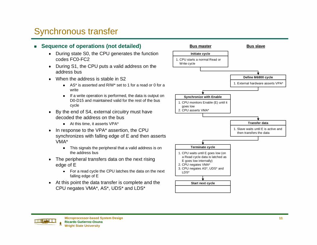
Synchronous transfer
g Sequence of operations (not detailed)n During state S0, the CPU generates the function
codes FC0-FC2n During S1, the CPU puts a valid address on the
address busn When the address is stable in S2
g AS* is asserted and R/W* set to 1 for a read or 0 for a write
g If a write operation is performed, the data is output on D0-D15 and maintained valid for the rest of the bus cycle
n By the end of S4, external circuitry must have decoded the address on the bus
g At this time, it asserts VPA*
n In response to the VPA* assertion, the CPU synchronizes with falling edge of E and then asserts VMA*
g This signals the peripheral that a valid address is on the address bus
n The peripheral transfers data on the next rising edge of E
g For a read cycle the CPU latches the data on the next falling edge of E
n At this point the data transfer is complete and the CPU negates VMA*, AS*, UDS* and LDS*
Initiate cycle
Define M6800 cycle
1. External hardware asserts VPA*
Synchronize with Enable
1. CPU monitors Enable (E) until it goes low
2. CPU asserts VMA*
Transfer data
1. Slave waits until E is active and then transfers the data
Terminate cycle
1. CPU waits until E goes low (on a Read cycle data is latched asE goes low internally)
2. CPU negates VMA*3. CPU negates AS*, UDS* and
LDS*
Bus master Bus slave
1. CPU starts a normal Read orWrite cycle
Start next cycle
Microprocessor-based System DesignRicardo Gutierrez-OsunaWright State University
12
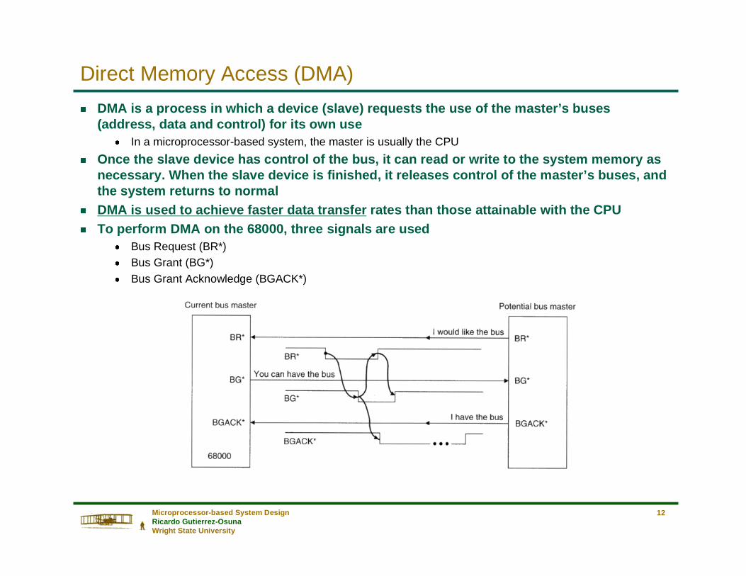
Direct Memory Access (DMA)
g DMA is a process in which a device (slave) requests the use of the master’s buses (address, data and control) for its own use
n In a microprocessor-based system, the master is usually the CPU
g Once the slave device has control of the bus, it can read or write to the system memory as necessary. When the slave device is finished, it releases control of the master’s buses, and the system returns to normal
g DMA is used to achieve faster data transfer rates than those attainable with the CPUg To perform DMA on the 68000, three signals are used
n Bus Request (BR*)n Bus Grant (BG*)n Bus Grant Acknowledge (BGACK*)

Microprocessor-based System DesignRicardo Gutierrez-OsunaWright State University
13
Why is DMA faster?
g Consider the problem of writing a block of memory to an output port, one byte at a time. The following tasks must be performed
n Initialize memory and output port addressesn Repeat until all bytes are transferred:
g Read byte from memoryg Write byte to output portg Increment memory addressg Check to see if all bytes transferredg Wait until output port ready for next byte
g With this approach, only a fraction of the memory cycles are used for the actual data transfer
n the speed of the data transfer is much less than the maximum rate at which data can be read from the memory
g DMA is performed with a device called DMA controller (DMAC), which can be thought of a very specialized microprocessor, except for
n unlike a data transfer performed by the CPU, no instructions need to be fetched during the transfer to tell the DMAC how to perform the transfer
n thus, all memory cycles are available for transferring data

Microprocessor-based System DesignRicardo Gutierrez-OsunaWright State University
14
DMAC operation
g A DMA transfer takes place in several stagesn Like with any other memory-mapped peripheral, the CPU first sets up the DMAC’s registers to define
g the quantity of data to be movedg the type of DMA operationg the direction of data transfer
n The DMAC is activated by a request for service from its associated peripheralg When the peripheral asserts REQ*, the DMAC requests control of the bus by
n asserting its BR* outputn waiting for a BG* response from the bus mastern asserting BGACK*
n Once the DMAC has control of the bus, it generates all timing signals needed to transfer data between peripheral and memory
n DMA transfers take place in one of two modes
g Burst mode: several operands are transferred in consecutive bus cycles
g Cycle stealing mode: the DMA relinquishes the system bus between successive data transfers allowing normal CPU processing to be interleaved

Microprocessor-based System DesignRicardo Gutierrez-OsunaWright State University
15
MC6800 pinout
We have already studied all the pins except for these three

Microprocessor-based System DesignRicardo Gutierrez-OsunaWright State University
16
System control pins
g Bus Error (BERR*)n When asserted, it indicates that something has gone wrong with the current bus cyclen For example, an access to an invalid memory address is generated by faulty software
g The external logic detects this error and asserts BERR* to inform the 68000
n The action taken by the 68000 when it recognizes BERR* is rather complex and depends on the state of HALT*. For simplicity we will state that it will either
g try to rerun the faulty cycle org will generate an exception, and the OS will deal with the bus error
g Halt (HALT*)n This I/O pin can be used for three purposes
g Used as an input: to force the 6800 to execute one cycle at a time (for debugging purposes)g Used as an input: to rerun a failed bus cycle (see BERR*)g Used as an output: when the 68000 finds itself in a situation it cannot recover from, it stops further processing and asserts
HATL* to indicate this situation
g Reset (RESET*)n Used as an input: the 68000 loads the SSP from M[$000000] and PC from M[$000004]
g The RESET* pin will be connected to the system’s hardware reset button
n Used as an output: when the processor executes the RESET command, it will assert RESET* pin to reset all external devices
g This command does not affect the internal state of the 68000, so it allows peripherals to be reset without resetting the CPU