Embed Size (px)
Citation preview
8/10/2019 Lecture 15 optics
http://slidepdf.com/reader/full/lecture-15-optics 1/26
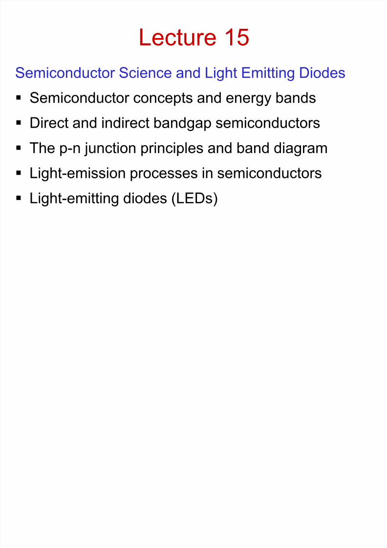
Lecture 15
Semiconductor Science and Light Emitting Diodes
! Semiconductor concepts and energy bands
!
Direct and indirect bandgap semiconductors
! The p-n junction principles and band diagram
! Light-emission processes in semiconductors
!
Light-emitting diodes (LEDs)
8/10/2019 Lecture 15 optics
http://slidepdf.com/reader/full/lecture-15-optics 2/26
8/10/2019 Lecture 15 optics
http://slidepdf.com/reader/full/lecture-15-optics 3/26
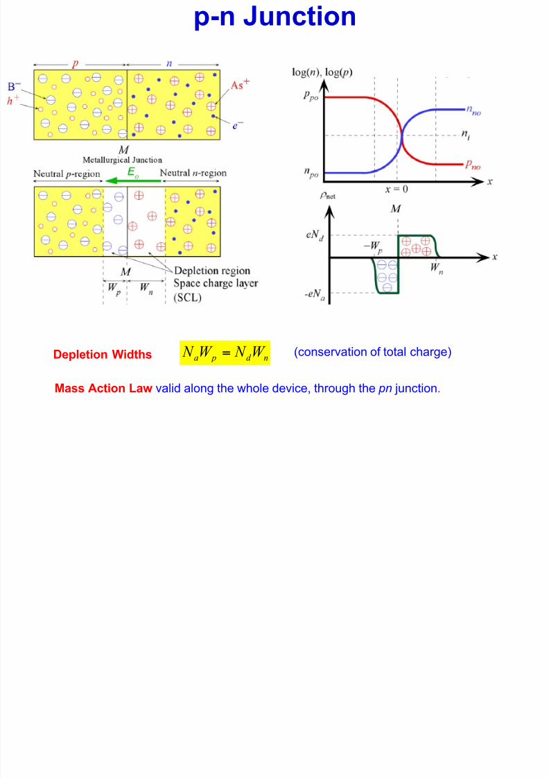
Mass Action Law valid along the whole device, through the pn junction.
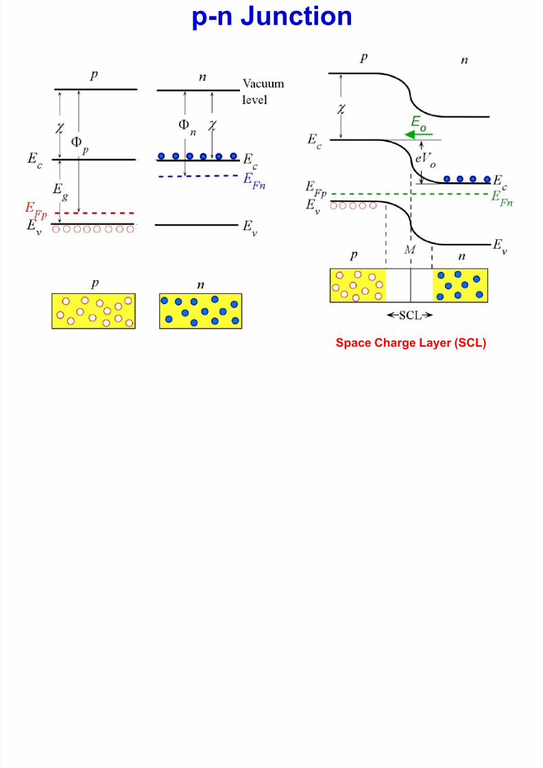
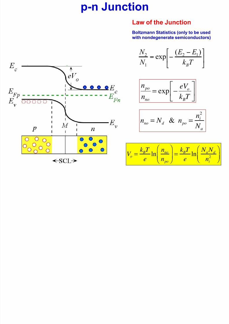
p-n Junction
Depletion Widths nd pa W N W N = (conservation of total charge)

8/10/2019 Lecture 15 optics
http://slidepdf.com/reader/full/lecture-15-optics 4/26
The electric field across the pn junction is found
by integrating !net.
p-n Junction
Built-in field
!
nd
o
W eN "=E
Built-in voltage
!
" )(net x
dx
d =
E
Field (E ) and net space charge density
! "=
x
W p
dx x x )(1
)( net # $
E
Field in depletion region
V o =
kT
e
ln N
a N
d
ni
2
!
" #
$
% & V
o = !
1
2
E 0W
0
8/10/2019 Lecture 15 optics
http://slidepdf.com/reader/full/lecture-15-optics 5/26
p-n Junction
Law of the Junction
Boltzmann Statistics (only to be usedwith nondegenerate semiconductors)
!"
#$%
& ''=
T k
E E
N
N
B
)(exp 12
1
2
n po
nno
= exp ! eV o
k BT
"
#$
%
&'
nno = N d & n po =
ni
2
N a
V o =k BT
e
ln nno
n po
!
" #
$
% & =
k BT
e
ln N a N d
ni
2
!
" #
$
% &
8/10/2019 Lecture 15 optics
http://slidepdf.com/reader/full/lecture-15-optics 6/26
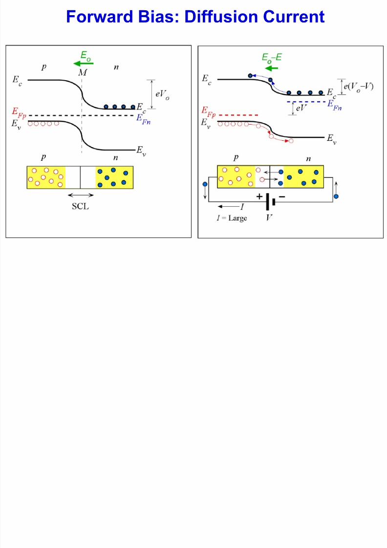
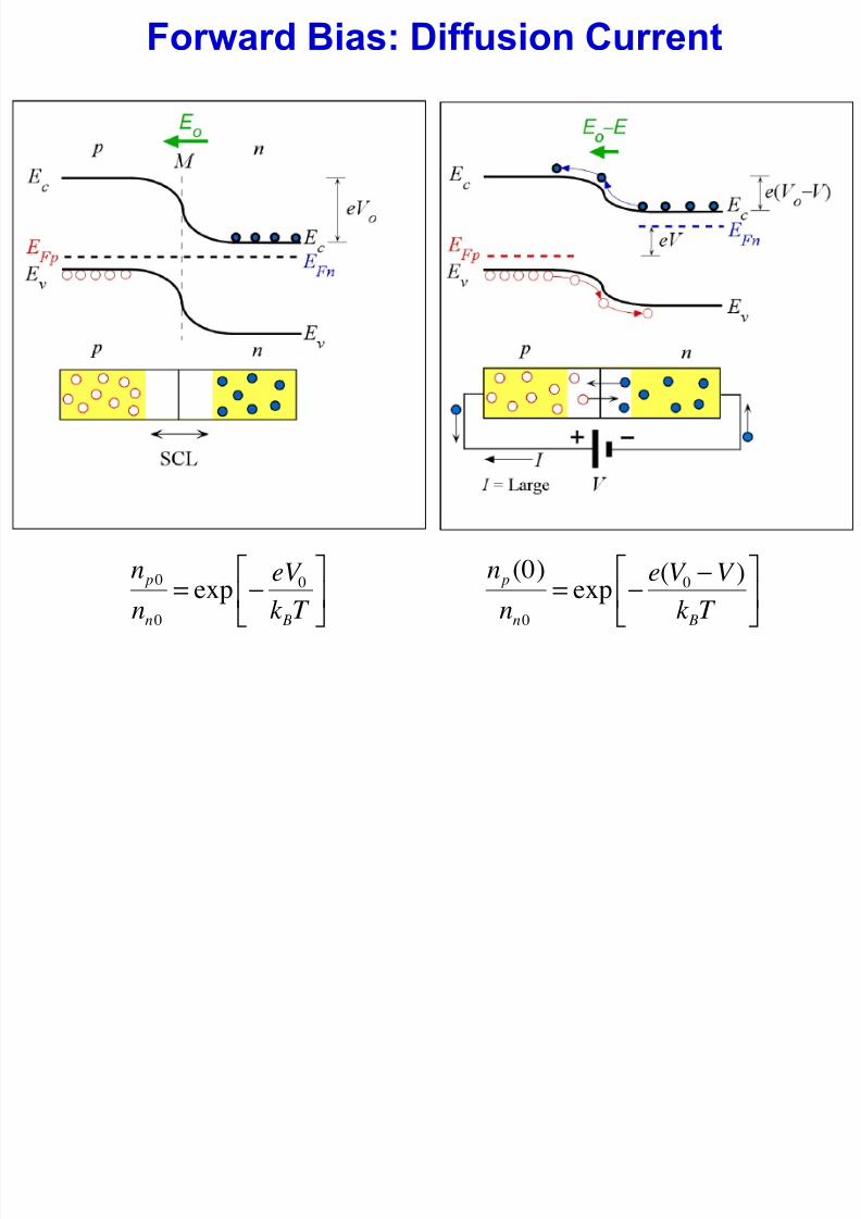
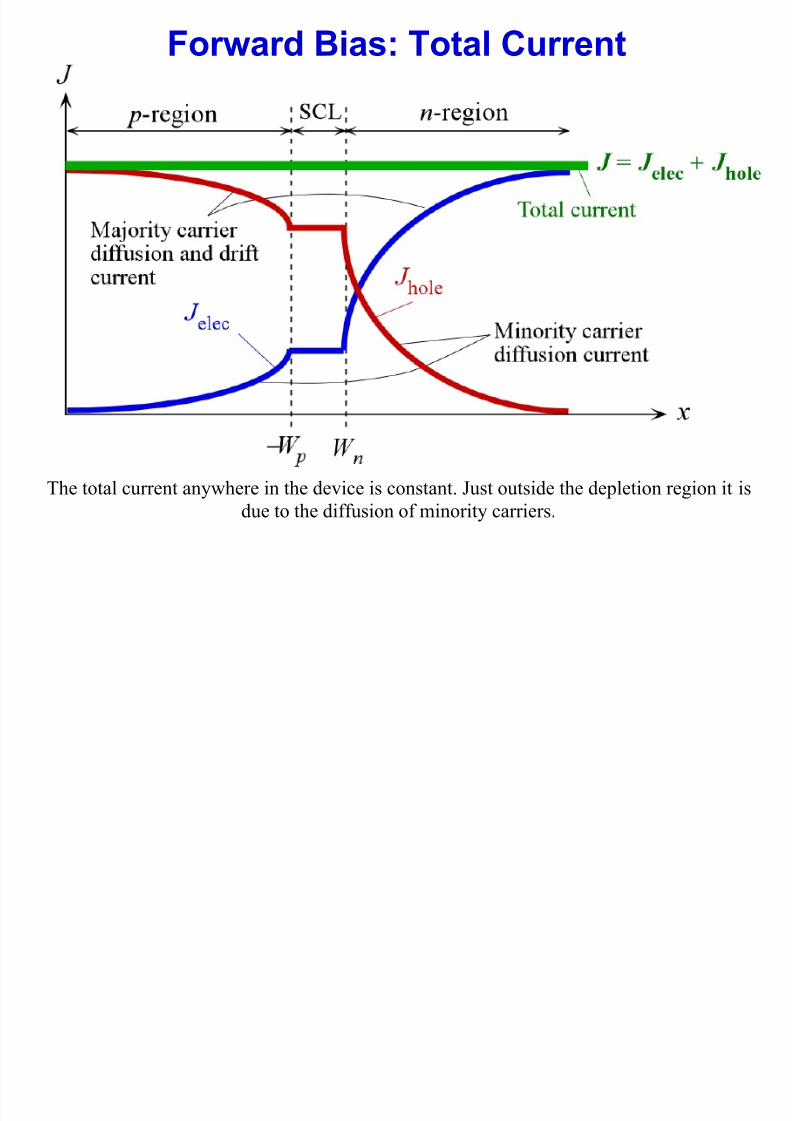
Forward Bias: Diffusion Current
8/10/2019 Lecture 15 optics
http://slidepdf.com/reader/full/lecture-15-optics 7/26
Forward Bias: Diffusion Current
n p0
nn0
=
exp !
eV 0
k BT
"
#$
%
&'
n p (0)
nn0
=
exp ! e(V 0 !V )
k BT
"
#$
%
&'

8/10/2019 Lecture 15 optics
http://slidepdf.com/reader/full/lecture-15-optics 8/26
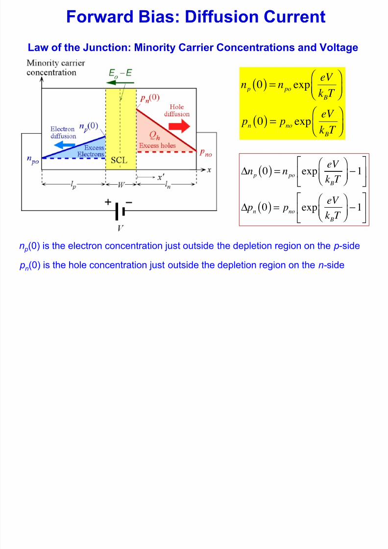
Law of the Junction: Minority Carrier Concentrations and Voltage
n p 0( ) = n po exp eV
k BT
! " #
$ % &
pn 0( ) = pno exp eV
k BT
!
" #
$
% &
Forward Bias: Diffusion Current
8/10/2019 Lecture 15 optics
http://slidepdf.com/reader/full/lecture-15-optics 9/26
Law of the Junction: Minority Carrier Concentrations and Voltage
n p 0( ) = n po exp eV
k BT
! " #
$ % &
pn 0( ) = pno exp eV
k BT
!
" #
$
% &
n p(0) is the electron concentration just outside the depletion region on the p-side
pn(0) is the hole concentration just outside the depletion region on the n-side
Forward Bias: Diffusion Current
!n p 0( ) = n po exp eV
k BT
" # $
% & ' (1
)
*+
,
-.
! pn 0( ) = pno exp eV k BT
" # $ % & ' (1)
*+ ,
-.
8/10/2019 Lecture 15 optics
http://slidepdf.com/reader/full/lecture-15-optics 10/26
Ideal diode (Shockley) equation
J = J so exp
eV
k BT
! " #
$ % & '1
(
)*
+
,-
J so =
eDh
Lh N
d
! " #
$ % & +
eDe
Le N
a
! " #
$ % &
'
()
*
+,ni
2
Reverse saturation current
Shockley Equation
Intrinsic concentration:
ni depends strongly on the material
(e.g. bandgap) and temperature
ni
2= N c N v exp !
E g
k BT
"
#
$%
&
'
8/10/2019 Lecture 15 optics
http://slidepdf.com/reader/full/lecture-15-optics 11/26

8/10/2019 Lecture 15 optics
http://slidepdf.com/reader/full/lecture-15-optics 12/26
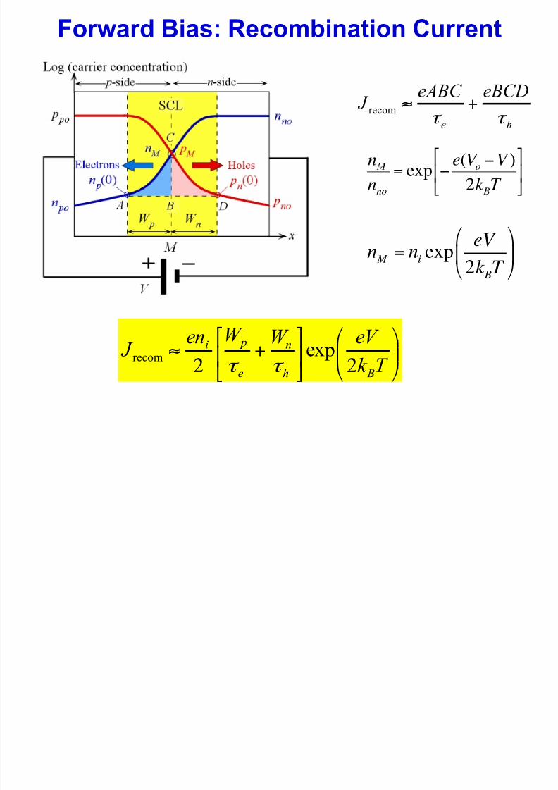
Forward Bias: Recombination Current
Forward biased pn junction, the injection of carriers and their recombination inthe SCL. Recombination of electrons and holes in the depletion region involves
the current supplying the carriers.

8/10/2019 Lecture 15 optics
http://slidepdf.com/reader/full/lecture-15-optics 13/26
Forward Bias: Recombination Current
A symmetrical pn junction for calculating the recombination current.

8/10/2019 Lecture 15 optics
http://slidepdf.com/reader/full/lecture-15-optics 14/26
Forward Bias: Diffusion Current
n p0
nn0
=
exp !
eV 0
k BT
"
#$
%
&'
n p (0)
nn0
=
exp ! e(V 0 !V )
k BT
"
#$
%
&'
8/10/2019 Lecture 15 optics
http://slidepdf.com/reader/full/lecture-15-optics 15/26
Forward Bias: Recombination Current
he
eBCDeABC J
! !
+"recom
n M
nno
= exp !e(V
o !V )
2k BT
"
#
$%
&
'
n M
= niexp
eV
2k BT
!
"#
$
%&
!!"
#$$%
&'(
)*+
,+-
T k
eV W W en J
Bh
n
e
pi
2exp
2recom
. .
8/10/2019 Lecture 15 optics
http://slidepdf.com/reader/full/lecture-15-optics 16/26
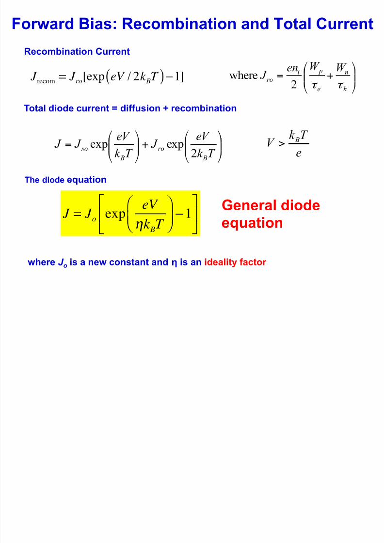
Forward Bias: Recombination and Total Current
Recombination Current
J recom = J ro[exp eV / 2k
BT ( )!1]
!!"
#$$%
&+!!
"
#$$%
&=
T k
eV J
T k
eV J J
B
ro
B
so
2expexp
Total diode current = diffusion + recombination
e
T k V B>
The diode equation
!!"#
$$%& +=
h
n
e
piro
W W en J ' ' 2
where
J = J o exp
eV
!k BT
" # $
% & ' (1)
*+ ,
-.
where J o
is a new constant and ! is an ideality factor
General diodeequation

8/10/2019 Lecture 15 optics
http://slidepdf.com/reader/full/lecture-15-optics 17/26
Typical I -V characteristics of Ge, Si and GaAs pn junctions as log( I ) vs. V . The slope
indicates e/(!k BT )
Typical I -V characteristics of Ge, Si and GaAs pn junctions
8/10/2019 Lecture 15 optics
http://slidepdf.com/reader/full/lecture-15-optics 18/26
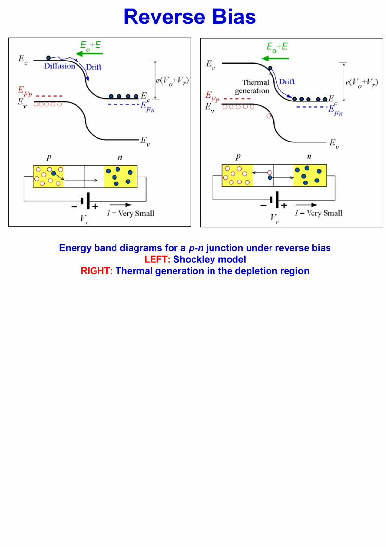
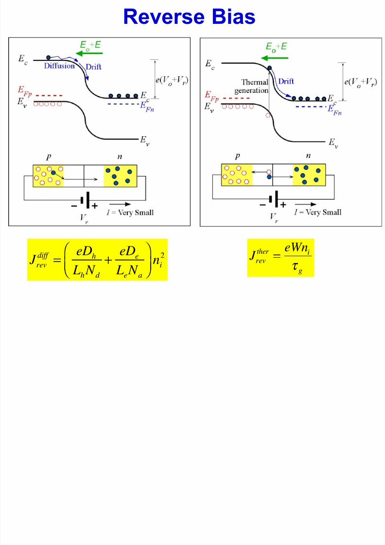
Reverse Bias
Energy band diagrams for a p-n junction under reverse biasLEFT: Shockley model
RIGHT: Thermal generation in the depletion region
8/10/2019 Lecture 15 optics
http://slidepdf.com/reader/full/lecture-15-optics 19/26
Reverse Bias
J revdiff
=eDh
Lh N d +
eDe
Le N a
!
" #
$
% & ni
2 J revther
=
eWni
! g

8/10/2019 Lecture 15 optics
http://slidepdf.com/reader/full/lecture-15-optics 20/26
Reverse BiasTotal Reverse Current
J rev
= eDh
Lh N d + eDe
Le N a! " #
$ % & ni
2+ eWni
' g
Mean thermal generation time0
Diffusion current in neutral regions
the Shockley reverse current
Thermal generation in depletion region
J = J o exp
eV
!k BT
"
# $
%
& ' (1
)
*+
,
-.

8/10/2019 Lecture 15 optics
http://slidepdf.com/reader/full/lecture-15-optics 21/26
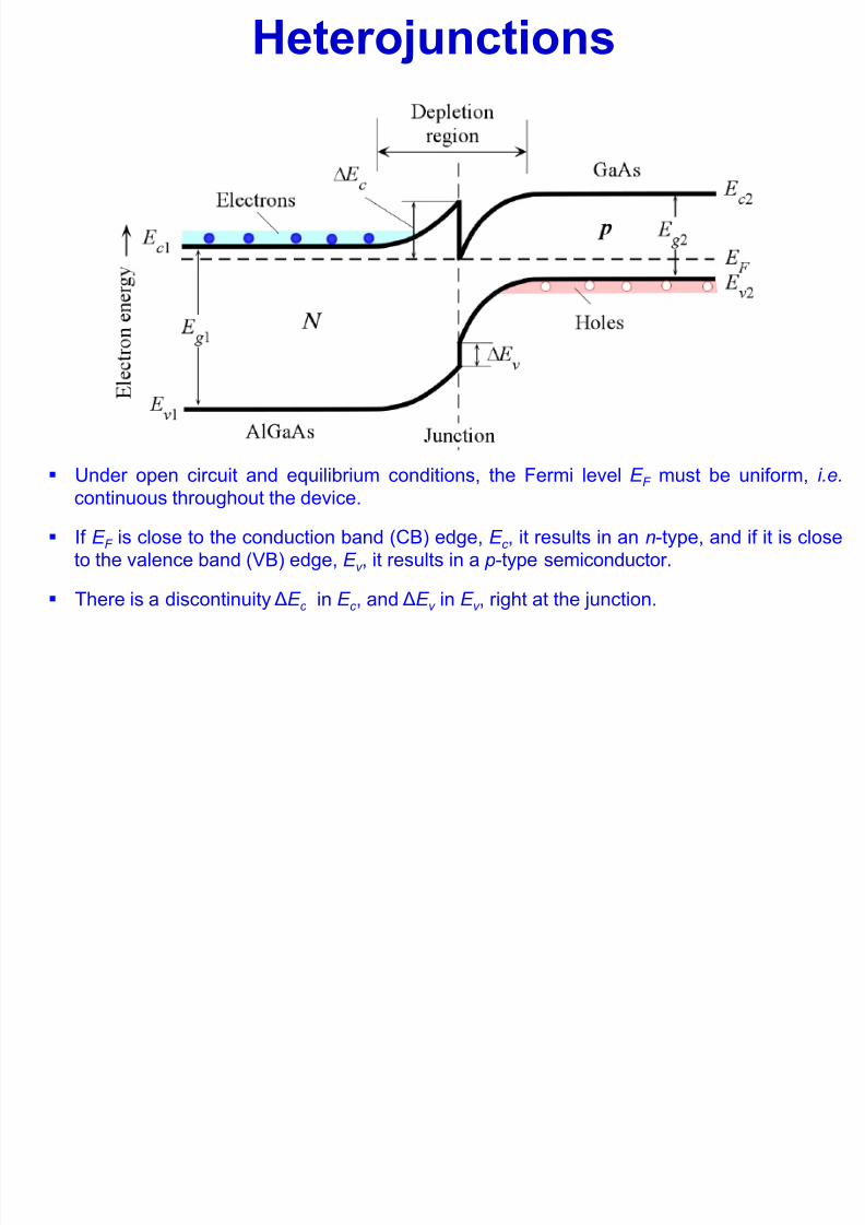
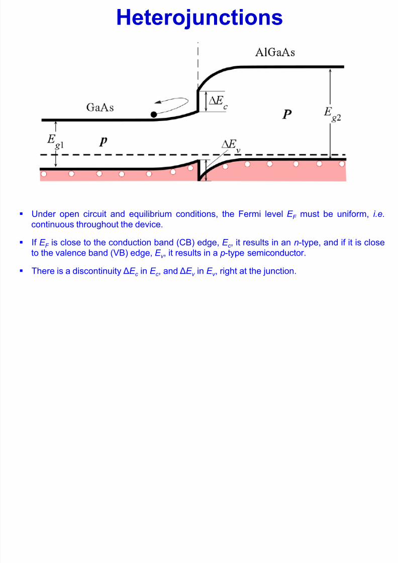
Heterojunctions
Two types of heterojunction and the definitions of band offsets, Type I and Type II between
two semiconductor crystals 1 and 2. Crystal 1 has a narrower bandgap E g 1 than E g 2 for
crystal 2. Note that the semiconductors are not in contact so that the Fermi level in each is
different. In this example, crystal 1 (GaAs) is p-type and crystal 2 (AlGaAs) is N-type.
8/10/2019 Lecture 15 optics
http://slidepdf.com/reader/full/lecture-15-optics 22/26
! Under open circuit and equilibrium conditions, the Fermi level E F must be uniform, i.e.
continuous throughout the device.
! If E F is close to the conduction band (CB) edge, E c , it results in an n-type, and if it is close
to the valence band (VB) edge, E v , it results in a p-type semiconductor.
!
There is a discontinuity "E c in E c , and "E v in E v , right at the junction.
Heterojunctions
8/10/2019 Lecture 15 optics
http://slidepdf.com/reader/full/lecture-15-optics 23/26
Heterojunctions
!
Under open circuit and equilibrium conditions, the Fermi level E F must be uniform, i.e.
continuous throughout the device.
! If E F is close to the conduction band (CB) edge, E c , it results in an n-type, and if it is close
to the valence band (VB) edge, E v , it results in a p-type semiconductor.
! There is a discontinuity "E c in E c , and "E v in E v , right at the junction.
8/10/2019 Lecture 15 optics
http://slidepdf.com/reader/full/lecture-15-optics 24/26
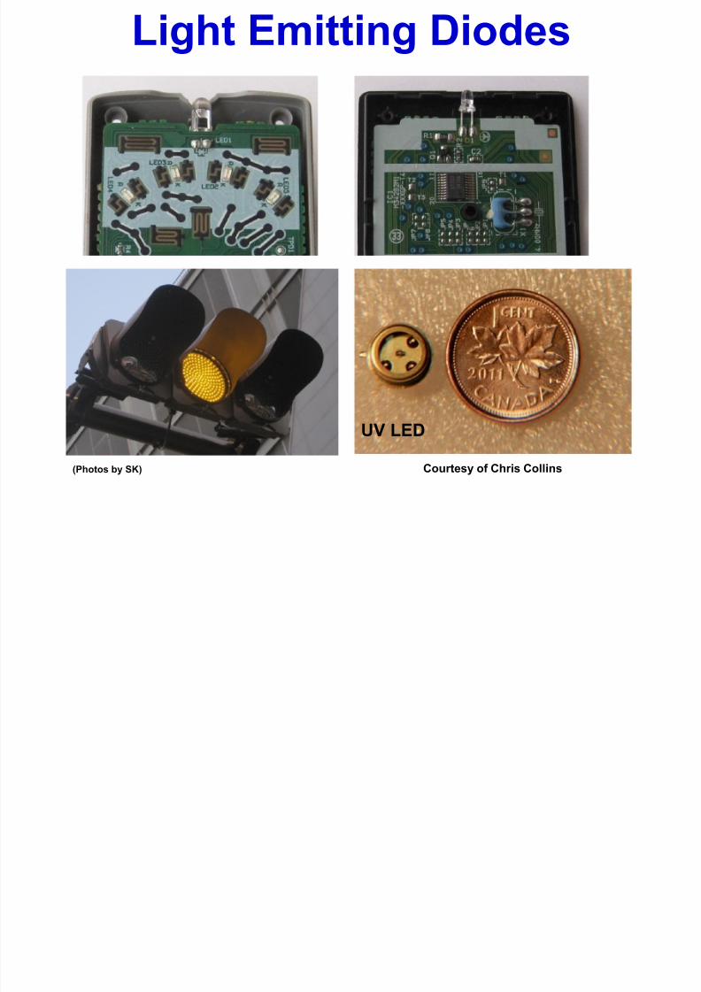
Light Emitting Diodes
UV LED
Courtesy of Chris Collins (Photos by SK)
8/10/2019 Lecture 15 optics
http://slidepdf.com/reader/full/lecture-15-optics 25/26

8/10/2019 Lecture 15 optics
http://slidepdf.com/reader/full/lecture-15-optics 26/26
Heterostructure High Density LEDS