Embed Size (px)
Citation preview

Lecture 9
Bipolar Junction Transistor (BJT)
BJT 1-1
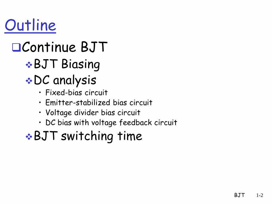
Outline
Continue BJT BJT Biasing DC analysis
• Fixed-bias circuit • Emitter-stabilized bias circuit • Voltage divider bias circuit • DC bias with voltage feedback circuit
BJT switching time
BJT 1-2
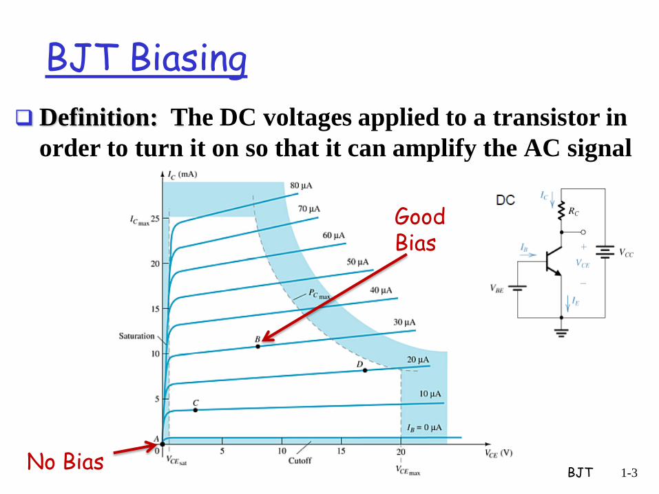
BJT Biasing
Definition: The DC voltages applied to a transistor in
order to turn it on so that it can amplify the AC signal
BJT 1-3 No Bias
Good Bias
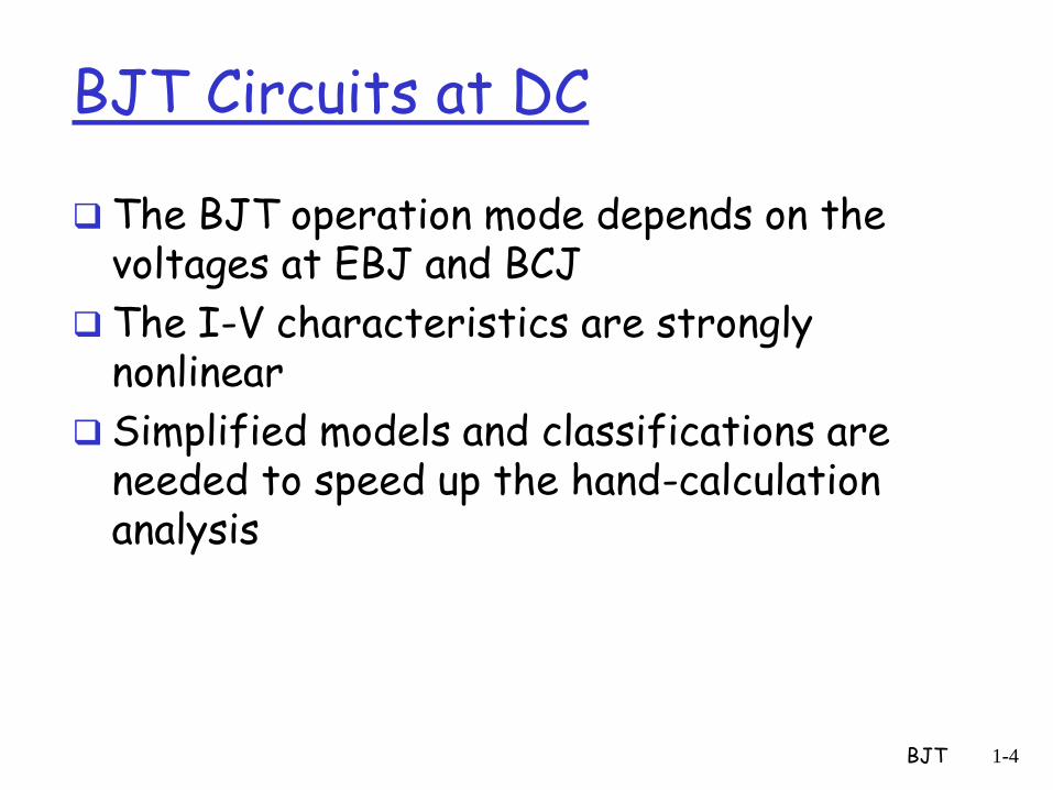
BJT Circuits at DC
The BJT operation mode depends on the voltages at EBJ and BCJ
The I-V characteristics are strongly nonlinear
Simplified models and classifications are needed to speed up the hand-calculation analysis
BJT 1-4
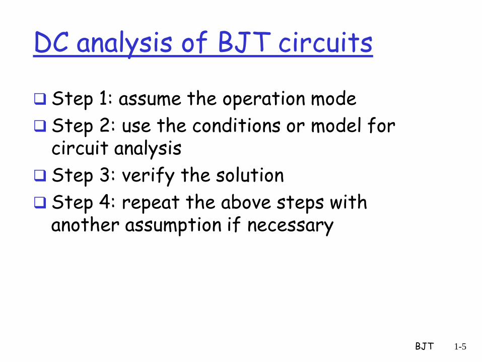
DC analysis of BJT circuits
Step 1: assume the operation mode
Step 2: use the conditions or model for circuit analysis
Step 3: verify the solution
Step 4: repeat the above steps with another assumption if necessary
BJT 1-5
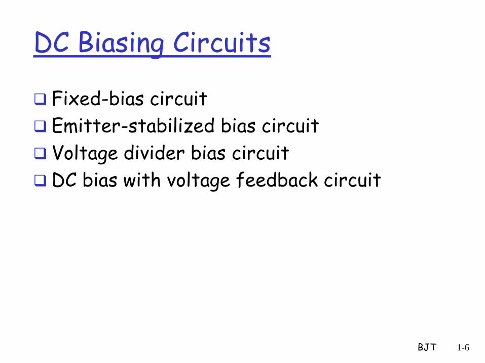
DC Biasing Circuits
Fixed-bias circuit
Emitter-stabilized bias circuit
Voltage divider bias circuit
DC bias with voltage feedback circuit
BJT 1-6
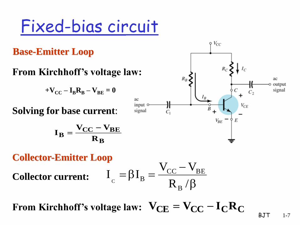
Fixed-bias circuit
BJT 1-7
Base-Emitter Loop
From Kirchhoff’s voltage law:
+VCC – IBRB – VBE = 0
Solving for base current:
B
BECCB
R
VVI
Collector-Emitter Loop
/R
VVII
B
BECCBC
Collector current:
From Kirchhoff’s voltage law: CCCCCE RIVV

Example (1)
BJT 1-8
Design the following circuit so that Ic = 2 mA and Vc= 5 V. For this particular transistor, β =100 and VBE=0.7 V
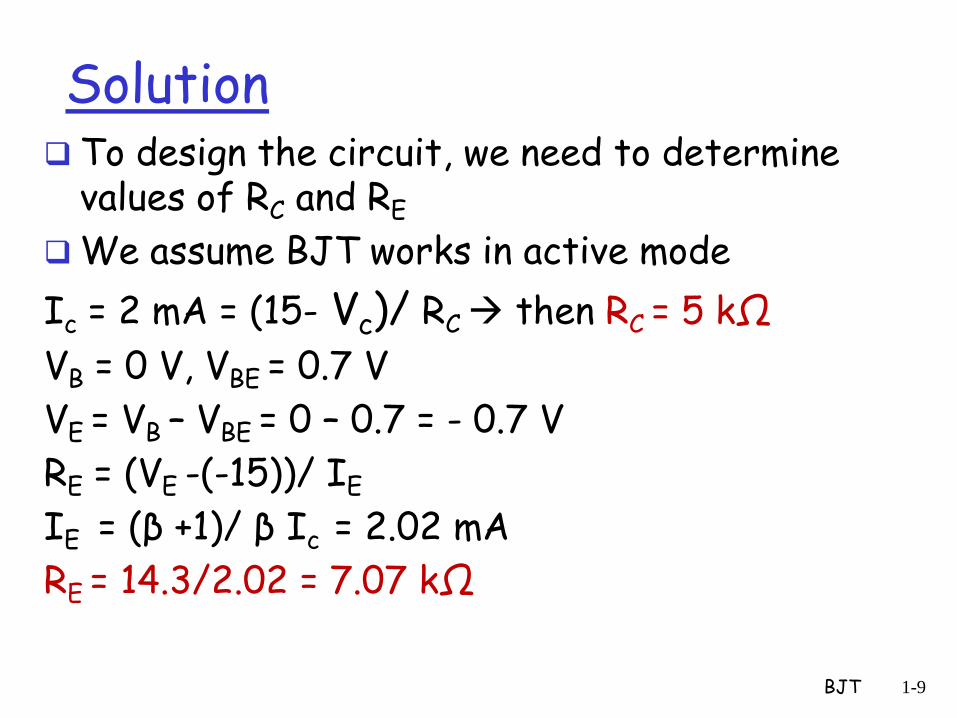
Solution To design the circuit, we need to determine
values of RC and RE
We assume BJT works in active mode
Ic = 2 mA = (15- Vc)/ RC then RC = 5 kΩ
VB = 0 V, VBE = 0.7 V
VE = VB – VBE = 0 – 0.7 = - 0.7 V
RE = (VE -(-15))/ IE
IE = (β +1)/ β Ic = 2.02 mA
RE = 14.3/2.02 = 7.07 kΩ
BJT 1-9
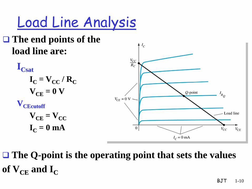
Load Line Analysis The end points of the
load line are:
BJT 1-10
ICsat
IC = VCC / RC
VCE = 0 V
VCEcutoff
VCE = VCC
IC = 0 mA
The Q-point is the operating point that sets the values
of VCE and IC

Circuit Values Affect the Q-Point
BJT 1-11
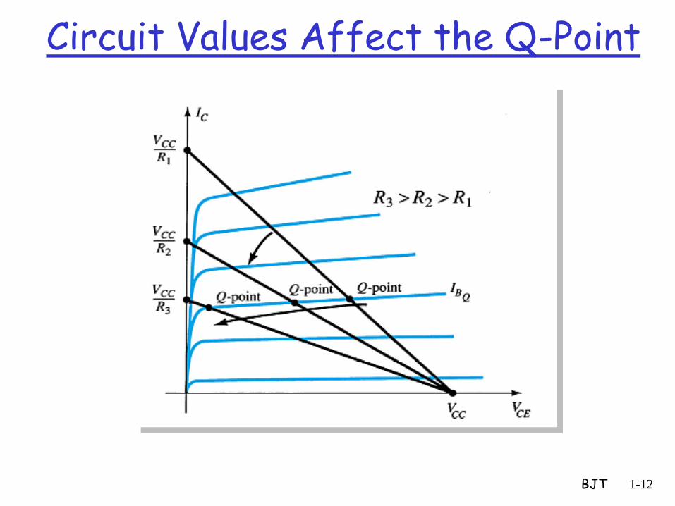
Circuit Values Affect the Q-Point
BJT 1-12

Circuit Values Affect the Q-Point
BJT 1-13

Example (2)
BJT 1-14
Given the load line and the defined Q-point, as shown in figure 2-a, determine the required values of VCC, RC, and RB for a fixed-bias configuration as depicted at figure 2-b.
Figure 2-a
Figure 2-b

Solution
BJT 1-15
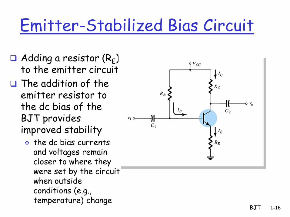
Emitter-Stabilized Bias Circuit
Adding a resistor (RE) to the emitter circuit
The addition of the emitter resistor to the dc bias of the BJT provides improved stability the dc bias currents
and voltages remain closer to where they were set by the circuit when outside conditions (e.g., temperature) change
BJT 1-16
Emitter-Stabilized Bias Circuit
BJT 1-17
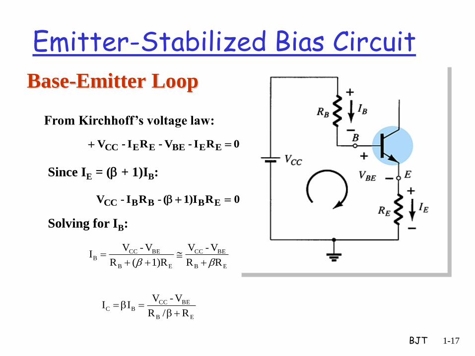
Base-Emitter Loop
From Kirchhoff’s voltage law:
0R1)I(-RI-V EBBBCC
0 RI-V-RI-V EEBEEECC
EB
BECC
EB
BECCB
RR
V-V
1)R(R
V-VI
Since IE = ( + 1)IB:
Solving for IB:
EB
BECCBC
R/R
V-VII
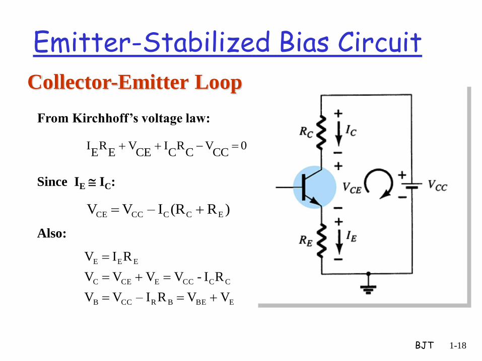
Emitter-Stabilized Bias Circuit
BJT 1-18
Collector-Emitter Loop
From Kirchhoff’s voltage law:
0 CC
VC
RC
I CE
V E
RE
I
Since IE IC:
)R (RI– V V ECCCCCE
Also:
EBEBRCCB
CCCCECEC
EEE
V V RI– V V
RI - V V V V
RI V

Voltage Divider Bias Circuit
This is a very stable bias circuit.
The currents and voltages are nearly independent of any variations in .
BJT 1-19

Approximate Analysis of Voltage Divider Bias Circuit
BJT 1-20
Where IB << I1 and I1 I2 :
Where RE > 10R2:
From Kirchhoff’s voltage law:
21
CC2B
RR
VRV
E
EE
R
VI
BEBE VVV
EECCCCCE RI RI V V
)R (RIV V
II
ECCCCCE
CE
Condition to be tested

Problem
Design the bias network for the silicon npn BJT circuit such that IE = 1mA, R1=22k Ω and R2=2.2kΩ, if the transistor has β equals 100.
BJT 1-21

DC Bias with Voltage Feedback Circuit Another way to
improve the stability of a bias circuit is to add a feedback path from collector to base
In this bias circuit the Q-point is only slightly dependent on the transistor beta,
BJT 1-22
DC Bias with Voltage Feedback Circuit
BJT 1-23
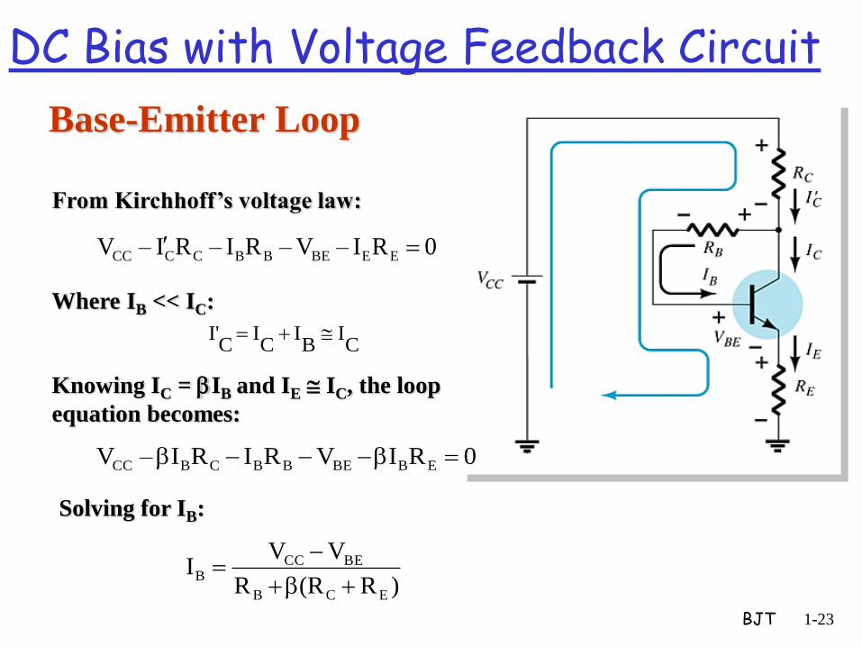
Base-Emitter Loop
)R(RR
VVI
ECB
BECCB
From Kirchhoff’s voltage law:
0RI–V–RI–RI– V EEBEBBCCCC
Where IB << IC:
CI
BI
CI
CI'
Knowing IC = IB and IE IC, the loop
equation becomes:
0RIVRIRI– V EBBEBBCBCC
Solving for IB:
DC Bias with Voltage Feedback Circuit
BJT 1-24
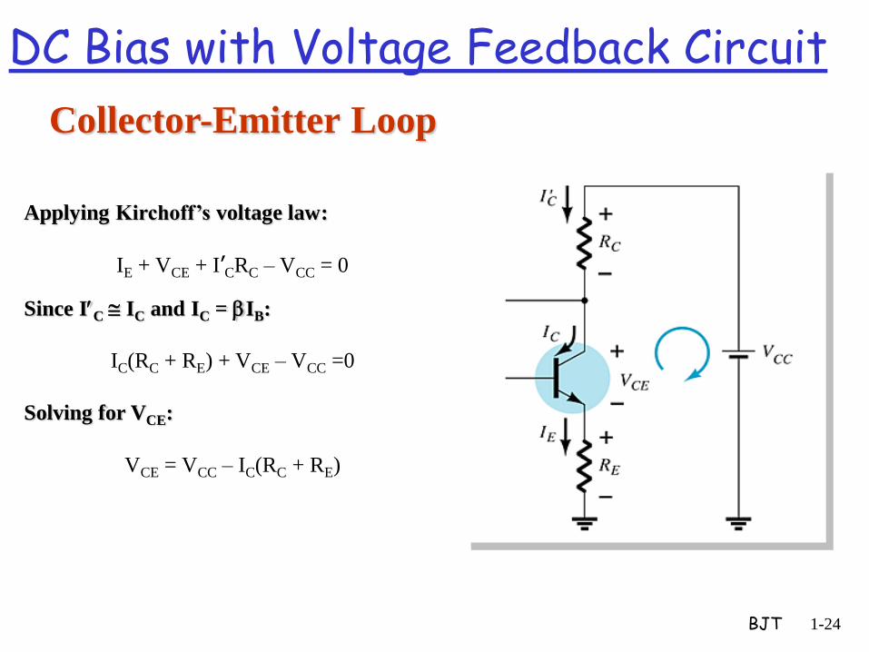
Collector-Emitter Loop
Applying Kirchoff’s voltage law:
IE + VCE + I’CRC – VCC = 0
Since IC IC and IC = IB:
IC(RC + RE) + VCE – VCC =0
Solving for VCE:
VCE = VCC – IC(RC + RE)
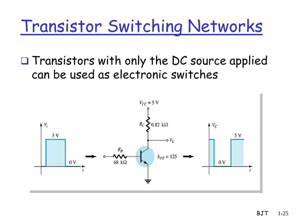
Transistor Switching Networks
Transistors with only the DC source applied can be used as electronic switches
BJT 1-25
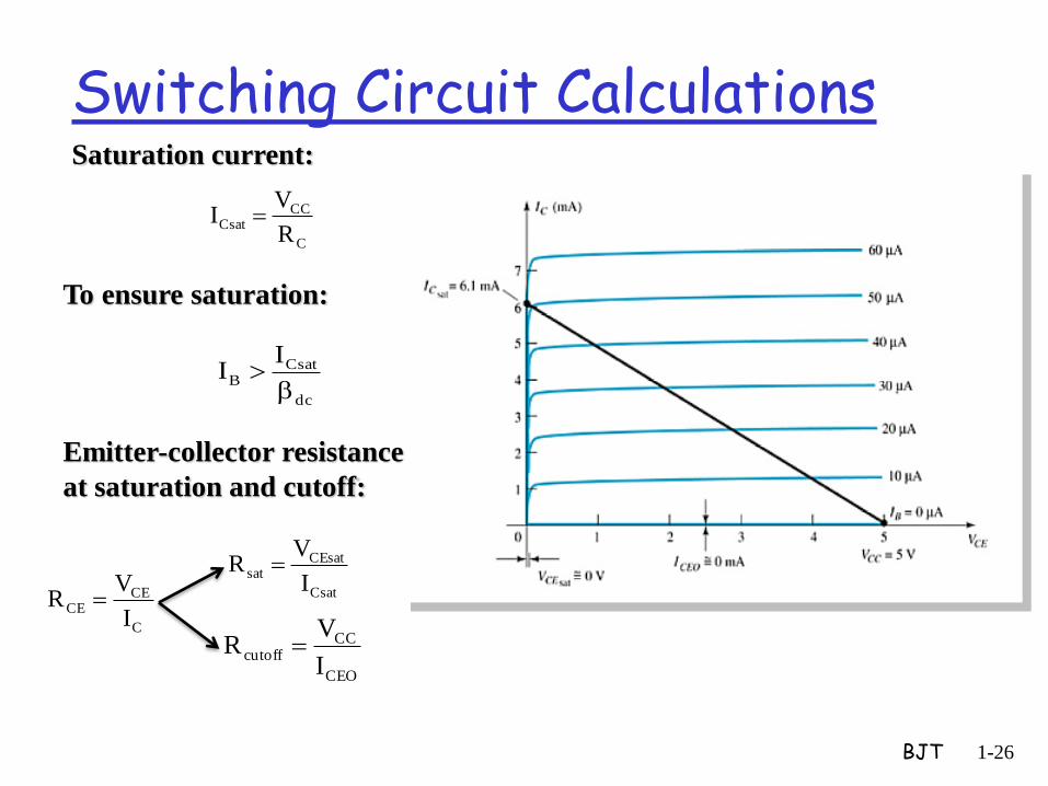
Switching Circuit Calculations
BJT 1-26
C
CCCsat
R
VI
dc
CsatB
II
Csat
CEsatsat
I
VR
CEO
CCcutoff
I
VR
Saturation current:
To ensure saturation:
Emitter-collector resistance
at saturation and cutoff:
C
CECE
I
VR
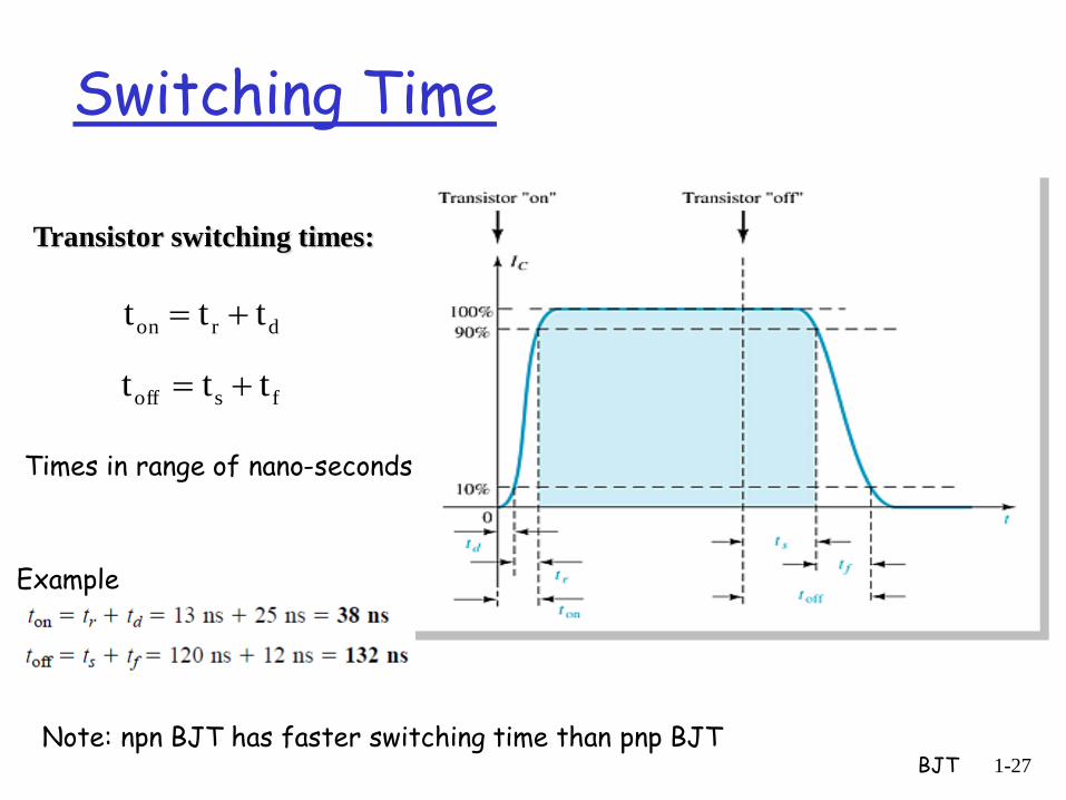
Switching Time
BJT 1-27
Transistor switching times:
dron ttt
fsoff ttt
Times in range of nano-seconds
Example
Note: npn BJT has faster switching time than pnp BJT

BJT 1-28
Lecture Summary
Covered material Continue BJT
Biasing DC analysis
• Fixed-bias circuit • Emitter-stabilized bias circuit • Voltage divider bias circuit • DC bias with voltage feedback
BJT switching time
Material to be covered next lecture
Continue BJT Continue DC analysis
• More examples
Introduction to ac signal analysis


![Toward Smart Moving Target Defense for Linux Container ...eng.staff.alexu.edu.eg/~bmokhtar/publications/LCN_paper.pdf · used Docker [7], an LXC-based container management tool hosted](https://img.pdfslide.net/doc/110x75/5f87c0278c4bbd28a559f377/toward-smart-moving-target-defense-for-linux-container-engstaffalexueduegbmokhtarpublicationslcnpaperpdf.jpg)