Embed Size (px)
DESCRIPTION
LInear voltage regulator thesis
Citation preview
A CAPACITOR-FREE LOW DROPOUT REGULATOR FOR LOW POWER
SYSTEM-ON-CHIP APPLICATIONS
Oscar Igor Robles Palacios
Dissertacao de Mestrado apresentada ao
Programa de Pos-graduacao em Engenharia
Eletrica, COPPE, da Universidade Federal do
Rio de Janeiro, como parte dos requisitos
necessarios a obtencao do tıtulo de Mestre em
Engenharia Eletrica.
Orientador: Antonio Petraglia
Rio de Janeiro
Agosto de 2013
A CAPACITOR-FREE LOW DROPOUT REGULATOR FOR LOW POWER
SYSTEM-ON-CHIP APPLICATIONS
Oscar Igor Robles Palacios
DISSERTACAO SUBMETIDA AO CORPO DOCENTE DO INSTITUTO
ALBERTO LUIZ COIMBRA DE POS-GRADUACAO E PESQUISA DE
ENGENHARIA (COPPE) DA UNIVERSIDADE FEDERAL DO RIO DE
JANEIRO COMO PARTE DOS REQUISITOS NECESSARIOS PARA A
OBTENCAO DO GRAU DE MESTRE EM CIENCIAS EM ENGENHARIA
ELETRICA.
Examinada por:
Prof. Antonio Petraglia, Ph.D.
Prof. Antonio Carneiro de Mesquita Filho, Dr.d’Etat
Prof. Marcio Nogueira de Souza, D.Sc.
RIO DE JANEIRO, RJ – BRASIL
AGOSTO DE 2013
Palacios, Oscar Igor Robles
A Capacitor-free Low Dropout Regulator for Low Power
System-on-Chip Applications/Oscar Igor Robles Palacios.
– Rio de Janeiro: UFRJ/COPPE, 2013.
XVIII, 113 p.: il.; 29, 7cm.
Orientador: Antonio Petraglia
Dissertacao (mestrado) – UFRJ/COPPE/Programa de
Engenharia Eletrica, 2013.
Referencias Bibliograficas: p. 111 – 113.
1. CMOS. 2. LDO. 3. SoC. 4. Dynamic Biasing.
5. Active Feedback. 6. Slew Rate Enhancement. I.
Petraglia, Antonio. II. Universidade Federal do Rio de
Janeiro, COPPE, Programa de Engenharia Eletrica. III.
Tıtulo.
iii
“Para odiar hay que querer
para destruir hay que hacer
y estoy orgulloso
de quererte romper
la cabeza contra la pared
Para dejar hay que beber
para morir primero
hay que nacer
siento ganas nuevamente
de tirarme a tus pies
y llevarte a mi morada otra vez
Si lo sembras lo recoges
y si esperas vas a entender
cuando las cosas salen
como no las espero
la vida me hace mas guerrero.”
Intoxicados - Nunca Quise
iv

Agradecimentos
A mis padres, Vıctor y Miryam, quienes nunca perdieron la fe en mı, inclusive en
momentos en los que parecıa perdido y sin rumbo.
A mis hermanos, Daniel, Vladimir y Karina, pues a medida que paso el tiempo
y enfrentaron nuevos desafıos, me ayudaron y me guiaron a enfrentar los mıos.
A mis cunados, Kathy y Fabio, porque no fue hasta hace poco que percibı todo
lo que aportan a nuestra familia y lo mucho que me alegra que formen parte de ella.
A Jorge, Lucas, Hernan, Santiago, Fede, Tincho y Miguel, los pibes de Rıo...
Ustedes se convirtieron en mi familia en esta ciudad y realmente no pude encontrar
mejores hermanos “cariocas”.
To Cossette, Eva, Carla and Disly, whose friendship and companionship made
me feel like I wasn’t the only foreigner trying to figure out this crazy but wonderful
city.
A Barbara, Marıa Marta, Andrea, Erika, Marco, Gonzalo y Federico, por los
buenos momentos, la buena energıa, las conversas tanto triviales como profundas y,
sobre todo, por su sincera amistad.
Aos meus colegas e amigos do mestrado e do laboratorio PADS, Jorge, Fabian,
Thiago e Gustavo... A gente viveu junto as penas e glorias da pesquisa e foi gratifi-
cante saber que eu nao era o unico louco apostando nesta area esquisita.
A Sergio, Karla, Karina, Francis, Ana Marıa, Fernando y Kristy, porque sin
importar lo mucho que me divertıa en Rıo, siempre me recordaron lo buena que era
mi vida en mi tierra y todas las cosas que hasta el dıa de hoy extrano de ella.
A Paolo y Hugo, amigos de toda la vida que buscaron su propio camino en tierras
extranjeras, long before I did, y cuyas charlas y life experience que compartimos a
lo largo de los anos me motivo a hacer mi propia senda.
Ao meu professor e orientador Antonio Petraglia, pelos conhecimentos e apoio
brindados durante todo o mestrado.
Finally, to everbody, mentioned or not, that took part of this incredible journey...
All of you brought joy to my days as a graduate student and turned this place into
a truly “cidade maravilhosa”!
Gracias! Obrigado! Thank you! Danke! Grazie! Merci!
v
Resumo da Dissertacao apresentada a COPPE/UFRJ como parte dos requisitos
necessarios para a obtencao do grau de Mestre em Ciencias (M.Sc.)
A CAPACITOR-FREE LOW DROPOUT REGULATOR FOR LOW POWER
SYSTEM-ON-CHIP APPLICATIONS
Oscar Igor Robles Palacios
Agosto/2013
Orientador: Antonio Petraglia
Programa: Engenharia Eletrica
Low-dropout regulators (LDOs) sao importantes blocos de gerenciamento de ener-
gia dentro de qualquer sistema eletronico. Eles sao responsaveis pela geracao de uma
fonte estavel e livre de espurias, o que e especialmente crıtico quando se trabalha
com circuitos sensıveis ao ruıdo. Para aplicacoes de System on Chip (SoC), onde
o uso da area e o consumo de energia devem ser otimizados, os LDOs aparecem
como uma opcao eficiente para a geracao de energia limpa devido a sua estrutura
relativamente simples e a necessidade de poucos componentes externos. Os princi-
pais objetivos no projeto de LDO sao minimizar o consumo de corrente quiescente
e evitar o uso de capacitores externos e, simultaneamente, conseguir estabilidade
elevada, regulacao precisa e uma rapida resposta. Nesta dissertacao, varias tecnicas
- tais como dynamic biasing, active feedback e slew rate enhancement - sao revis-
tas e aplicadas a estrutura basica de um LDO a fim de atingir os objetivos acima
mencionados. O circuito foi implementado utilizando um processo CMOS 180nm.
O LDO e desenvolvido para fornecer 1.8 V para uma carga maxima de 50 mA, com
um dropout mınimo de 200 mV e uma corrente quiescente maxima de 58 µA. O
LDO projetado e estavel em qualquer situacao, mesmo quando nenhuma carga esta
presente, assumindo uma capacidade de carga maxima de 50 pF . Uma rejeicao da
fonte de alimentacao maxima de -40 dB @ 10 kHz e assegurada. O overshoot e
undershoot sao menores do que 200 mV para mudancas de carga completa dentro
de 1 µs, e o tempo de recuperacao e inferior a 3 µs.
vi
Abstract of Dissertation presented to COPPE/UFRJ as a partial fulfillment of the
requirements for the degree of Master of Science (M.Sc.)
A CAPACITOR-FREE LOW DROPOUT REGULATOR FOR LOW POWER
SYSTEM-ON-CHIP APPLICATIONS
Oscar Igor Robles Palacios
August/2013
Advisor: Antonio Petraglia
Department: Electrical Engineering
Low-dropout regulators (LDOs) are key power management blocks within any
electronic system. They are in charge of generating a spurious free and stable supply,
which is critical specially when working with noise sensitive circuits. For System
on Chip (SoC) applications, where area usage and power consumption are to be
optimized, LDOs appear as an efficient option for clean supply generation due to
their relatively simple structure and few external components. The main objectives
in LDO design are the minimization of the quiescent current consumption and the
avoidance of external capacitors, while achieving high stability, accurate regulation
and fast response. In this dissertation, several techniques - such as, dynamic biasing,
active feedback, and slew rate enhancement - are reviewed and applied to the basic
structure of an LDO in order to attain the aforementioned goals. The circuit was
implemented using a 180nm CMOS process. The developed LDO supplies 1.8V to
a maximum load of 50 mA, with a minimum dropout of 200 mV and a maximum
quiescent current of 58 µA. The designed LDO is stable in any scenario, even when
no load is present, assuming a maximum load capacitance of 50 pF . A maximum
power supply rejection of -40 dB @ 10 kHz is ensured. The maximum overshoot
and undershoot are less than 200 mV for full load current changes in 1 µs, and the
recovery time is less than 3 µs.
vii
Contents
List of Figures xi
List of Tables xvi
List of Acronyms xvii
1 Introduction 1
1.1 Motivation . . . . . . . . . . . . . . . . . . . . . . . . . . . . . . . . . 1
1.2 Objectives . . . . . . . . . . . . . . . . . . . . . . . . . . . . . . . . . 2
1.3 Methodology . . . . . . . . . . . . . . . . . . . . . . . . . . . . . . . 3
1.4 Structure of Work . . . . . . . . . . . . . . . . . . . . . . . . . . . . . 4
2 Bibliographical Revision 5
2.1 Error Amplifier . . . . . . . . . . . . . . . . . . . . . . . . . . . . . . 6
2.1.1 Class AB Structure . . . . . . . . . . . . . . . . . . . . . . . . 6
2.1.2 Operational Transconductance Amplifier . . . . . . . . . . . . 9
2.1.3 Flipped Voltage Follower . . . . . . . . . . . . . . . . . . . . . 10
2.2 LDO Structure . . . . . . . . . . . . . . . . . . . . . . . . . . . . . . 13
2.2.1 Active Feedback . . . . . . . . . . . . . . . . . . . . . . . . . . 13
2.2.2 Adaptive Biasing . . . . . . . . . . . . . . . . . . . . . . . . . 16
2.2.3 Dynamic Biasing . . . . . . . . . . . . . . . . . . . . . . . . . 19
2.2.4 Resonance Factors Adjustment . . . . . . . . . . . . . . . . . 23
2.2.5 Hybrid Cascode . . . . . . . . . . . . . . . . . . . . . . . . . . 26
3 Schematic Design 29
3.1 LDO Structure . . . . . . . . . . . . . . . . . . . . . . . . . . . . . . 29
3.2 Small Signal Analysis . . . . . . . . . . . . . . . . . . . . . . . . . . . 30
3.3 Large Signal Analysis . . . . . . . . . . . . . . . . . . . . . . . . . . . 40
3.4 Transistor Dimensioning . . . . . . . . . . . . . . . . . . . . . . . . . 45
4 Layout Design 51
4.1 Power Transistor . . . . . . . . . . . . . . . . . . . . . . . . . . . . . 51
viii
4.2 Differential Pair . . . . . . . . . . . . . . . . . . . . . . . . . . . . . . 52
4.3 Reference Current Mirrors . . . . . . . . . . . . . . . . . . . . . . . . 53
4.4 Array of Capacitors . . . . . . . . . . . . . . . . . . . . . . . . . . . . 54
4.5 Feedback Resistors . . . . . . . . . . . . . . . . . . . . . . . . . . . . 55
4.6 LDO Full Layout Design . . . . . . . . . . . . . . . . . . . . . . . . . 56
5 Simulations Results 59
5.1 Steady-State Response . . . . . . . . . . . . . . . . . . . . . . . . . . 60
5.1.1 Nominal Performance . . . . . . . . . . . . . . . . . . . . . . . 60
5.1.2 Temperature Sweep . . . . . . . . . . . . . . . . . . . . . . . . 62
5.1.3 Monte Carlo Analysis . . . . . . . . . . . . . . . . . . . . . . . 65
5.2 Stability . . . . . . . . . . . . . . . . . . . . . . . . . . . . . . . . . . 69
5.2.1 Nominal Performance . . . . . . . . . . . . . . . . . . . . . . . 69
5.2.2 Temperature Sweep . . . . . . . . . . . . . . . . . . . . . . . . 71
5.2.3 Monte Carlo Analysis . . . . . . . . . . . . . . . . . . . . . . . 75
5.3 Power Supply Rejection Ratio . . . . . . . . . . . . . . . . . . . . . . 80
5.3.1 Nominal Performance . . . . . . . . . . . . . . . . . . . . . . . 80
5.3.2 Temperature Sweep . . . . . . . . . . . . . . . . . . . . . . . . 82
5.3.3 Monte Carlo Analysis . . . . . . . . . . . . . . . . . . . . . . . 86
5.4 Load Transient Response . . . . . . . . . . . . . . . . . . . . . . . . . 91
5.4.1 Nominal Performance . . . . . . . . . . . . . . . . . . . . . . . 91
5.4.2 Temperature Sweep . . . . . . . . . . . . . . . . . . . . . . . . 93
5.4.3 Monte Carlo Analysis . . . . . . . . . . . . . . . . . . . . . . . 95
5.5 Load Regulation . . . . . . . . . . . . . . . . . . . . . . . . . . . . . 96
5.5.1 Nominal Performance . . . . . . . . . . . . . . . . . . . . . . . 96
5.5.2 Temperature Sweep . . . . . . . . . . . . . . . . . . . . . . . . 97
5.5.3 Monte Carlo Analysis . . . . . . . . . . . . . . . . . . . . . . . 98
5.6 Line Transient Response . . . . . . . . . . . . . . . . . . . . . . . . . 99
5.6.1 Nominal Performance . . . . . . . . . . . . . . . . . . . . . . . 99
5.6.2 Temperature Sweep . . . . . . . . . . . . . . . . . . . . . . . . 102
5.6.3 Monte Carlo Analysis . . . . . . . . . . . . . . . . . . . . . . . 103
5.7 Line Regulation . . . . . . . . . . . . . . . . . . . . . . . . . . . . . . 105
5.7.1 Nominal Performance . . . . . . . . . . . . . . . . . . . . . . . 105
5.7.2 Temperature Sweep . . . . . . . . . . . . . . . . . . . . . . . . 106
5.7.3 Monte Carlo Analysis . . . . . . . . . . . . . . . . . . . . . . . 107
5.8 Performance Summary . . . . . . . . . . . . . . . . . . . . . . . . . . 108
6 Conclusions 109
6.1 General Conclusions . . . . . . . . . . . . . . . . . . . . . . . . . . . 109
6.2 Future Work . . . . . . . . . . . . . . . . . . . . . . . . . . . . . . . . 110
ix

Bibliography 111
x
List of Figures
2.1 Schematic of classic LDO. . . . . . . . . . . . . . . . . . . . . . . . . . 5
2.2 Schematic of type-N class AB amplifier. . . . . . . . . . . . . . . . . . . 7
2.3 Small-signal model of class AB amplifier. . . . . . . . . . . . . . . . . . 8
2.4 Schematic of differential OTA cell. . . . . . . . . . . . . . . . . . . . . . 9
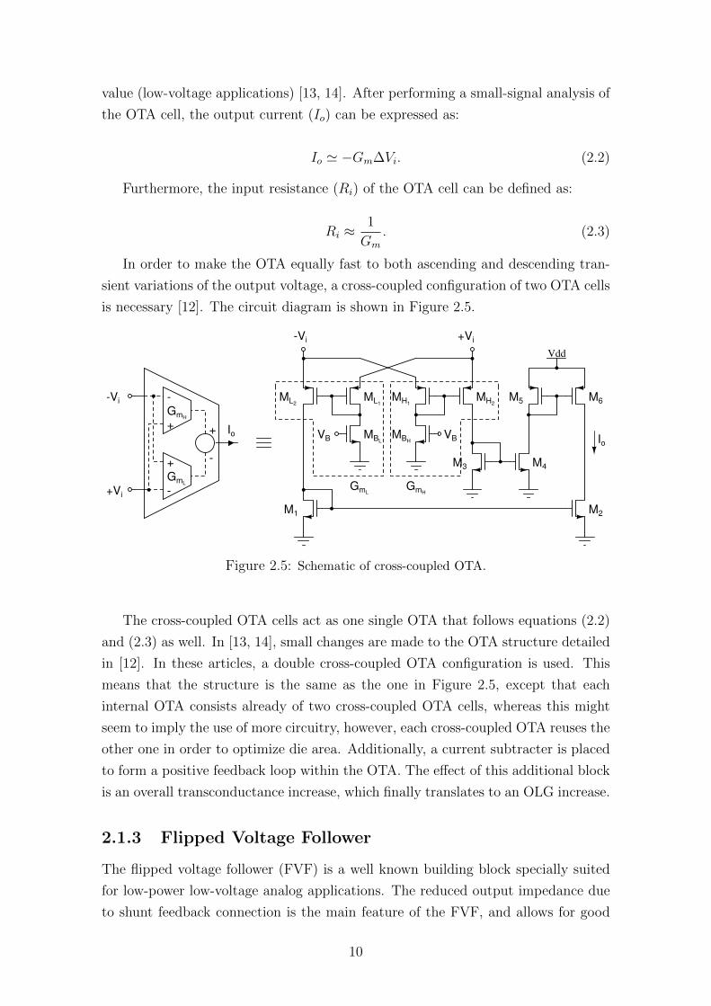
2.5 Schematic of cross-coupled OTA. . . . . . . . . . . . . . . . . . . . . . . 10
2.6 Schematic of single-transistor FVF-based LDO. . . . . . . . . . . . . . . 11
2.7 Schematic of preset voltage generator for FVF-based LDO. . . . . . . . . 12
2.8 Schematic of 2-transistor FVF-based LDO. . . . . . . . . . . . . . . . . 12
2.9 Small-signal model of simple LDO with active feedback. . . . . . . . . . . 14
2.10 Adaptive biasing operating principles. . . . . . . . . . . . . . . . . . . . 18
2.11 Conceptual Schematic of LDO with Adaptive Biasing. . . . . . . . . . . . 18
2.12 Dynamic biasing operating principal. . . . . . . . . . . . . . . . . . . . . 20
2.13 Schematic of voltage spike detection circuit through capacitive coupling. . 20
2.14 Behavior of voltage spike detection circuit through capacitive coupling. . . 21
2.15 Transient behavior of load current and output voltage of an LDO. . . . . 22
2.16 Frequency response of an LDO for different loads. . . . . . . . . . . . . . 23
2.17 Schematic of LDO with Q-reduction technique. . . . . . . . . . . . . . . 25
2.18 Small-signal equivalent circuit of LDO with Q-reduction technique. . . . . 25
2.19 Schematic of LDO with classic cascode compensation. . . . . . . . . . . . 27
2.20 Schematic of LDO with hybrid cascode compensation. . . . . . . . . . . . 28
3.1 Conceptual Schematic of the proposed LDO. . . . . . . . . . . . . . . . . 30
3.2 Small signal model of the proposed LDO. . . . . . . . . . . . . . . . . . 31
3.3 Small signal model of the adaptive bias voltage generator. . . . . . . . . . 32
3.4 Small signal model of the adaptive active feedback block. . . . . . . . . . 32
3.5 Simplified small signal model of the adaptive active feedback block. . . . . 33
3.6 Simplified small signal model of the proposed LDO. . . . . . . . . . . . . 33
3.7 Pole-zero mapping of the LDO. (a) Heavy-load condition. (b) Medium-
load condition. (c) Light-load condition. . . . . . . . . . . . . . . . . . . 39
3.8 Transient response of the LDO. . . . . . . . . . . . . . . . . . . . . . . 40
3.9 Push-pull output stage of the EA. . . . . . . . . . . . . . . . . . . . . . 40
xi
3.10 Schematic of the error amplifier. . . . . . . . . . . . . . . . . . . . . . . 41
3.11 Output transconductor of the SRE block. . . . . . . . . . . . . . . . . . 42
3.12 Schematic of the SRE block. . . . . . . . . . . . . . . . . . . . . . . . . 43
3.13 Schematic of the LDO. . . . . . . . . . . . . . . . . . . . . . . . . . . . 48
3.14 (a) Open-loop response of the LDO small signal model for different load
currents (Iout). (b) Zoomed-in viewed around the UGF. . . . . . . . . . . 50
4.1 Layout design mockup of the power transistor. . . . . . . . . . . . . . . . 52
4.2 Layout design mockup of the differential pair. . . . . . . . . . . . . . . . 53
4.3 Layout design mockup of the reference current mirrors. . . . . . . . . . . 54
4.4 Layout design mockup of the array of capacitors. . . . . . . . . . . . . . 55
4.5 Layout design mockup of the feedback resistors. . . . . . . . . . . . . . . 56
4.6 Layout design of the LDO. . . . . . . . . . . . . . . . . . . . . . . . . . 57
5.1 Quiescent current (IQ). . . . . . . . . . . . . . . . . . . . . . . . . . . . 60
5.2 Output power (Pout). . . . . . . . . . . . . . . . . . . . . . . . . . . . . 61
5.3 Power efficiency (η). . . . . . . . . . . . . . . . . . . . . . . . . . . . . 61
5.4 Temperature sweep of the quiescent current (IQ). . . . . . . . . . . . . . 62
5.5 Temperature sweep of the output power (Pout). . . . . . . . . . . . . . . 62
5.6 Temperature sweep of the power efficiency (η). . . . . . . . . . . . . . . 63
5.7 Temperature sweep of the η@500uA. . . . . . . . . . . . . . . . . . . . . 63
5.8 Temperature sweep of the quiescent current (top left corner), output volt-
age (top right corner), output power (bottom left corner), and power effi-
ciency (bottom right corner) for ILOAD = 0 mA. . . . . . . . . . . . . . . 64
5.9 Temperature sweep of the quiescent current (top left corner), output volt-
age (top right corner), output power (bottom left corner), and power effi-
ciency (bottom right corner) for ILOAD = 5 mA. . . . . . . . . . . . . . . 65
5.10 Temperature sweep of the quiescent current (top left corner), output volt-
age (top right corner), output power (bottom left corner), and power effi-
ciency (bottom right corner) for ILOAD = 50 mA. . . . . . . . . . . . . . 65
5.11 Monte carlo analysis of the quiescent current (IQ). . . . . . . . . . . . . 66
5.12 Monte carlo analysis of the output power (Pout). . . . . . . . . . . . . . . 66
5.13 Monte carlo analysis of the power efficiency (η). . . . . . . . . . . . . . . 67
5.14 Monte carlo analysis of the η@500uA. . . . . . . . . . . . . . . . . . . . 67
5.15 Monte carlo analysis of the quiescent current (top left corner), output
voltage (top right corner), output power (bottom left corner), and power
efficiency (bottom right corner) for ILOAD = 0 mA. . . . . . . . . . . . . 68
5.16 Monte carlo analysis of the quiescent current (top left corner), output
voltage (top right corner), output power (bottom left corner), and power
efficiency (bottom right corner) for ILOAD = 5 mA. . . . . . . . . . . . . 68
xii
5.17 Monte carlo analysis of the quiescent current (top left corner), output
voltage (top right corner), output power (bottom left corner), and power
efficiency (bottom right corner) for ILOAD = 50 mA. . . . . . . . . . . . 69
5.18 Open-loop response for different load currents (ILOAD). . . . . . . . . . . 70
5.19 Zoomed-in view of the open-loop response for different load currents. . . . 70
5.20 Temperature sweep of the open-loop response for ILOAD = 0 mA. . . . . . 71
5.21 Zoomed-in view of the temperature sweep of the open-loop response for
ILOAD = 0 mA. . . . . . . . . . . . . . . . . . . . . . . . . . . . . . . 71
5.22 Temperature sweep of the open-loop response for ILOAD = 5 mA. . . . . . 72
5.23 Zoomed-in view of the temperature sweep of the open-loop response for
ILOAD = 5 mA. . . . . . . . . . . . . . . . . . . . . . . . . . . . . . . 72
5.24 Temperature sweep of the open-loop response for ILOAD = 50 mA. . . . . 73
5.25 Zoomed-in view of the temperature sweep of the open-loop response for
ILOAD = 50 mA. . . . . . . . . . . . . . . . . . . . . . . . . . . . . . . 73
5.26 Temperature sweep of the phase margin (left) and unity gain frequency
(right) for ILOAD = 0 mA. . . . . . . . . . . . . . . . . . . . . . . . . . 74
5.27 Temperature sweep of the phase margin (left) and unity gain frequency
(right) for ILOAD = 5 mA. . . . . . . . . . . . . . . . . . . . . . . . . . 74
5.28 Temperature sweep of the phase margin (left) and unity gain frequency
(right) for ILOAD = 50 mA. . . . . . . . . . . . . . . . . . . . . . . . . 75
5.29 Monte carlo analysis of the open-loop response for ILOAD = 0 mA. . . . . 76
5.30 Zoomed-in view of the montecarlo analysis of the open-loop response for
ILOAD = 0 mA. . . . . . . . . . . . . . . . . . . . . . . . . . . . . . . 76
5.31 Monte carlo analysis of the open-loop response for ILOAD = 5 mA. . . . . 77
5.32 Zoomed-in view of the montecarlo analysis of the open-loop response for
ILOAD = 5 mA. . . . . . . . . . . . . . . . . . . . . . . . . . . . . . . 77
5.33 Monte carlo analysis of the open-loop response for ILOAD = 50 mA. . . . 78
5.34 Zoomed-in view of the montecarlo analysis of the open-loop response for
ILOAD = 50 mA. . . . . . . . . . . . . . . . . . . . . . . . . . . . . . . 78
5.35 Monte carlo analysis of the phase margin (left) and unity gain frequency
(right) for ILOAD = 0 mA. . . . . . . . . . . . . . . . . . . . . . . . . . 79
5.36 Monte carlo analysis of the phase margin (left) and unity gain frequency
(right) for ILOAD = 5 mA. . . . . . . . . . . . . . . . . . . . . . . . . . 79
5.37 Monte carlo analysis of the phase margin (left) and unity gain frequency
(right) for ILOAD = 50 mA. . . . . . . . . . . . . . . . . . . . . . . . . 80
5.38 PSRR for different load currents (ILOAD). . . . . . . . . . . . . . . . . . 81
5.39 Zoomed-in view of the PSRR for different load currents (ILOAD). . . . . . 81
5.40 Temperature sweep of the PSRR for ILOAD = 0 mA. . . . . . . . . . . . 82
5.41 Zoomed-in view of the temperature sweep of the PSRR for ILOAD = 0 mA. 82
xiii
5.42 Temperature sweep of the PSRR for ILOAD = 5 mA. . . . . . . . . . . . 83
5.43 Zoomed-in view of the temperature sweep of the PSRR for ILOAD = 5 mA. 83
5.44 Temperature sweep of the PSRR for ILOAD = 50 mA. . . . . . . . . . . . 84
5.45 Zoomed-in view of the temperature sweep of the PSRR for ILOAD = 50 mA. 84
5.46 Temperature sweep of the PSRR@10kHz for ILOAD = 0 mA. . . . . . . . 85
5.47 Temperature sweep of the PSRR@10kHz for ILOAD = 5 mA. . . . . . . . 85
5.48 Temperature sweep of the PSRR@10kHz for ILOAD = 50 mA. . . . . . . 86
5.49 Monte carlo analysis of the PSRR for ILOAD = 0 mA. . . . . . . . . . . . 86
5.50 Zoomed-in view of the monte carlo analysis of the PSRR for ILOAD = 0
mA. . . . . . . . . . . . . . . . . . . . . . . . . . . . . . . . . . . . . 87
5.51 Monte carlo analysis of the PSRR for ILOAD = 5 mA. . . . . . . . . . . . 87
5.52 Zoomed-in view of the monte carlo analysis of the PSRR for ILOAD = 5
mA. . . . . . . . . . . . . . . . . . . . . . . . . . . . . . . . . . . . . 88
5.53 Monte carlo analysis of the PSRR for ILOAD = 50 mA. . . . . . . . . . . 88
5.54 Zoomed-in view of the monte carlo analysis of the PSRR for ILOAD = 50
mA. . . . . . . . . . . . . . . . . . . . . . . . . . . . . . . . . . . . . 89
5.55 Monte carlo analysis of the PSRR@10kHz for ILOAD = 0 mA. . . . . . . 89
5.56 Monte carlo analysis of the PSRR@10kHz for ILOAD = 5 mA. . . . . . . 90
5.57 Monte carlo analysis of the PSRR@10kHz for ILOAD = 50 mA. . . . . . 90
5.58 Transient load current (ILOAD). . . . . . . . . . . . . . . . . . . . . . . 91
5.59 Zoomed-in view of the transient load current (ILOAD). . . . . . . . . . . 91
5.60 Load transient response. . . . . . . . . . . . . . . . . . . . . . . . . . . 92
5.61 Zoomed-in view of the load transient response. . . . . . . . . . . . . . . 92
5.62 Temperature sweep of the load transient response. . . . . . . . . . . . . . 93
5.63 Zoomed-in view of the temperature sweep of the load transient response. . 94
5.64 Temperature sweep of the undershoot (top left corner), overshoot (top
right corner), undershoot settling time (bottom left corner), and overshoot
settling time (bottom right corner). . . . . . . . . . . . . . . . . . . . . 94
5.65 Monte carlo analysis of the load transient response. . . . . . . . . . . . . 95
5.66 Zoomed-in view of the monte carlo analysis of the load transient response. 95
5.67 Monte carlo analysis of the undershoot (top left corner), overshoot (top
right corner), undershoot settling time (bottom left corner), and overshoot
settling time (bottom right corner). . . . . . . . . . . . . . . . . . . . . 96
5.68 Load regulation. . . . . . . . . . . . . . . . . . . . . . . . . . . . . . . 97
5.69 Temperature sweep of the load regulation. . . . . . . . . . . . . . . . . . 97
5.70 Temperature sweep of the load regulation coefficient (LoR). . . . . . . . . 98
5.71 Monte carlo analysis of the load regulation. . . . . . . . . . . . . . . . . 99
5.72 Monte carlo analysis of the load regulation coefficient (LoR). . . . . . . . 99
5.73 Transient input supply voltage (Vsupp). . . . . . . . . . . . . . . . . . . . 100
xiv
5.74 Zoomed-in view of the transient input supply voltage (Vsupp). . . . . . . . 100
5.75 Line transient response. . . . . . . . . . . . . . . . . . . . . . . . . . . 101
5.76 Zoomed-in view of the line transient response. . . . . . . . . . . . . . . . 101
5.77 Temperature sweep of the line transient response. . . . . . . . . . . . . . 102
5.78 Zoomed-in view of the temperature sweep of the line transient response. . 102
5.79 Temperature sweep of the overshoot (top left corner), undershoot (top
right corner), overshoot settling time (bottom left corner), and undershoot
settling time (bottom right corner). . . . . . . . . . . . . . . . . . . . . 103
5.80 Monte carlo analysis of the line transient response. . . . . . . . . . . . . 104
5.81 Zoomed-in view of the monte carlo analysis of the line transient response. 104
5.82 Monte carlo analysis of the overshoot (top left corner), undershoot (top
right corner), overshoot settling time (bottom left corner), and undershoot
settling time (bottom right corner). . . . . . . . . . . . . . . . . . . . . 105
5.83 Line regulation. . . . . . . . . . . . . . . . . . . . . . . . . . . . . . . . 105
5.84 Temperature sweep of the line regulation. . . . . . . . . . . . . . . . . . 106
5.85 Temperature sweep of the line regulation coefficient (LiR). . . . . . . . . 107
5.86 Monte carlo analysis of the line regulation. . . . . . . . . . . . . . . . . . 107
5.87 Monte carlo analysis of the line regulation coefficient (LiR). . . . . . . . . 108
xv
List of Tables
3.1 LDO specifications. . . . . . . . . . . . . . . . . . . . . . . . . . . . . 45
3.2 CMOS extracted parameters. . . . . . . . . . . . . . . . . . . . . . . 47
3.3 CMOS mathematical models. . . . . . . . . . . . . . . . . . . . . . . 48
3.4 LDO design. . . . . . . . . . . . . . . . . . . . . . . . . . . . . . . . . 49
5.1 Steady-state nominal performance summary. . . . . . . . . . . . . . . 60
5.2 Load current based DC nominal performance summary. . . . . . . . . 61
5.3 Steady-state temperature sweep performance summary. . . . . . . . . 64
5.4 Load current based DC temperature sweep performance summary. . . 64
5.5 Steady-state monte carlo analysis performance summary. . . . . . . . 67
5.6 Load current based DC monte carlo performance summary. . . . . . . 69
5.7 Stability performance summary. . . . . . . . . . . . . . . . . . . . . . 70
5.8 Stability temperature sweep performance summary. . . . . . . . . . . 75
5.9 Stability monte carlo analysis performance summary. . . . . . . . . . 80
5.10 PSRR nominal performance summary. . . . . . . . . . . . . . . . . . 81
5.11 PSRR temperature sweep performance summary. . . . . . . . . . . . 86
5.12 PSRR monte carlo analysis performance summary. . . . . . . . . . . 90
5.13 Load transient response nominal performance summary. . . . . . . . . 93
5.14 Load transient response temperature sweep performance summary. . . 94
5.15 Load transient response monte carlo analysis performance summary. . 96
5.16 Load regulation nominal performance summary. . . . . . . . . . . . . 97
5.17 Load regulation temperature sweep performance summary. . . . . . . 98
5.18 Load regulation monte carlo analysis performance summary. . . . . . 98
5.19 Line transient response nominal performance summary. . . . . . . . . 101
5.20 Line transient response temperature sweep performance summary. . . 103
5.21 Line transient response monte carlo analysis performance summary. . 104
5.22 Line regulation nominal performance summary. . . . . . . . . . . . . 106
5.23 Line regulation temperature sweep performance summary. . . . . . . 106
5.24 Line regulation monte carlo analysis performance summary. . . . . . . 108
5.25 LDO performance summary. . . . . . . . . . . . . . . . . . . . . . . . 108
xvi
List of Acronyms
ASIC Application-Specific Integrated Circuit, p. 2
CAD Computer-Aided Design, p. 56
CMOS Complementary Metal-Oxide Semiconductor, p. 1
EA Error Amplifier, p. 5
EM Electromigration, p. 51
ESR Equivalent Series Resistance, p. 5
FVF Flipped Voltage Follower, p. 10
GBW Gain-Bandwidth, p. 46
ICMR Input Common-Mode Range, p. 9
LDO Low-Dropout Regulator, p. vii
LHP Left-Hand Plane, p. 6
MOSFET Metal-Oxide-Semiconductor Field-Effect Transistor, p. 11
OLG Open-Loop Gain, p. 7
Op-Amp Operational Amplifier, p. 5
OTA Operational Transconductance Amplifier, p. 7
PDK Process Design Kit, p. 47
PM Phase Margin, p. 17
PSRR Power Supply Rejection Ratio, p. 1
RC Resistance-Capacitance, p. 20
RHP Right-Hand Plane, p. 7
xvii

SoC System on Chip, p. vii
SR Slew Rate, p. 8
SRE Slew Rate Enhancement, p. 29
UGF Unity Gain Frequency, p. 2
xviii
Chapter 1
Introduction
This work intends to show the entire design - up to the physical implementation
using a 180 nm CMOS (Complementary Metal Oxide Semiconductor) process - of
an LDO that presents high stability, high PSRR (Power Supply Rejection Ratio),
and a fast transient response without the usage of any external components, such
as capacitors. This LDO is a critical block of power management units, since it is
meant to provide a clean and stable voltage supply for all highly sensitive analog
circuits within an energy measurement SoC, which is the main application of this
work. This type of SoC comprises both digital and analog circuitry, which are in
most cases placed inside the die with considerable proximity to each other. Thus,
the sensitive analog circuits must be isolated from the noise caused by the switching
nature of the digital circuits. Furthermore, due to the necessity to avoid external
components, several new techniques are applied to the traditional LDO topology.
Hence, this dissertation will focus on the analysis of this new architecture, which
mainly consists in the study of its behavior in both the frequency and time domains.
1.1 Motivation
LDOs have been one of the most essential building blocks in any Power Manage-
ment Unit for quite some time. As a consequence, they have been a vastly popular
choice among all sorts of electronic systems, where a stable voltage supply must
be guaranteed regardless of any changes in the input voltage supply, current output
load, or temperature. Depending on how sudden and significant the changes in both
the input supply and output load, most LDOs may require an output capacitor in
order to provide a charge/discharge outlet when the LDO is not fast enough to
handle the aforementioned variations. Moreover, the output capacitor usually sets
the dominant pole and works with an in-series resistor to generate a zero in the
frequency response of the loop, which improves both the frequency stability and
the PSRR performance of the LDO. However, as in any other field of electronics,
1
the trend is always to reduce the area usage, which applies to both the die and the
board. As new fabrication processes appear, the minimum dimensions get smaller
(nano-scale), which allows the electronic industry to demand the same results but
inside a much smaller package. Thus, with so many portable applications emerging,
output-capacitorless LDOs became a very promising research topic.
As the complexity of the portable applications grows, a SoC, instead of a simple
ASIC (Application-Specific Integrated Circuit), appears as a more suitable choice.
This, in turn, implies the coexistence of both digital and analog circuits within the
same die. As a consequence, the LDO becomes a necessity since analog circuits must
be shielded from the noise generated by the switching of the digital signals. Since
this noise may have components in the scale of kilohertz as well as megahertz, the
LDO must posses a good PSRR performance over a wide frequency range. Moreover,
some SoCs can withhold a large circuit density, which derives in the use of not one
but several LDOs in order to power up different analog blocks inside the system.
This reduces the crosstalk effect and helps to mitigate the load-transient voltage
spikes caused by the bonding wire inductors.
Another trend established by this growth of portable applications is the need
to reduce the power consumption. Both supply operating voltage and current con-
sumption of the circuits are decreasing rapidly in order to meet this new requisite.
The former is a direct consequence of the new fabrication processes, which decrease
not only the minimum dimensions, but also the threshold voltage of the transistors,
thereby allowing an abatement of the operating supply voltage. The latter is related
to the use of batteries as the input supply; the lower the current consumption, the
longer the lifetime of the battery. As a result, low voltage and low quiescent current
LDOs have become an attractive option for this type of applications.
1.2 Objectives
The purpose of this work is the realization of an output-capacitorless LDO that
presents frequency stability for all load conditions, high PSRR performance for a
wide frequency range, fast transient response and high current efficiency. Thus,
several State-of-the-Art techniques will be studied in order to improve both the
frequency and transient responses of the circuit, while reducing the current con-
sumption.
The main goal is to achieve frequency stability even when there is no load present,
while also attaining a high unity-gain-frequency (UGF), which has to be at least 1
MHz, specially for high load currents. This becomes a challenge since the LDO
must be fully integrated, which means no external capacitor can be used to set the
dominant pole of the frequency response. Even though no external capacitor must
2
be used, there will be a load capacitance generated by the parasitic capacitances
of the power distribution metal paths inside the microchip. In this case, the load
capacitance is not expected to surpass the 50 pF value. Moreover, achieving the
frequency stability specification while maintaining the current consumption at a
minimum is not an easy task. Nevertheless, this specification must be met in order
to deliver a state-of-the-art LDO.
The idea is to use this LDO to supply every low voltage sub-circuit of the SoC.
Thereby, according to the specification of the 180 nm CMOS process, the required
supply voltage will be 1.8 V , with a maximum load current of 50 mA. Besides
the supply voltage and current load, the PSRR specification is the one that defines
the performance of the LDO. The more rejection to the supply noise, the cleaner
the output voltage signal, which translates to a better regulation. As mentioned in
Section 1.1, the noise present in the unregulated supply could manifest in different
frequencies, and therefore the PSRR specification must be stated with magnitude
and frequency. For this specific design, a PSRR of at most −40 dB @ 10 kHz must
be guaranteed.
Delivering a fast LDO is also important. The circuit must be able to respond to
sudden changes in both the output current load, and the input voltage supply. The
LDO must be able to respond to full load current changes of 1 µs, with an overshoot
and undershoot no greater than 200 mV in the regulated output. Similarly, this
circuit has to be able to withstand a 5 µs voltage shift of the input supply within
the range of 2.0 and 2.5 V , with voltage peaks lower than 50 mV . The constraints
on the overshoots and undershoots are established to avoid damages in the circuitry.
1.3 Methodology
A thorough research on fully integrated LDOs was conducted in order to gather
information on the most recent techniques and results. Every topology proposal
was analyzed in order to understand its contributions, as well as its shortcomings.
This allowed for a specific combination of a few techniques that work well together
and deliver a high performance LDO.
The study and modeling of the modifications done to the traditional LDO
schematic were the starting point of the process. After the selection was completed,
the design was initiated with the establishment of the high level structure specifica-
tions. This, in turn, led to initial simulations with some ideal internal sub-blocks in
order to verify the performance of the entire system.
Once the high level structure was verified, the specifications for the internal sub-
blocks, such as the error amplifier, were drawn. From those specifications, the design
of all the circuits was performed.
3
Later on, several simulations were executed for validation purposes. Further-
more, a simulation that verify the performance of the circuit outside of the nominal
conditions was necessary in order to assure the proper behavior of the system under
a stress environment. Hence, a Monte Carlo analysis, which statistically emulates
process variations as well as mismatch effects, was the final one to be conducted.
After the Monte Carlo analysis delivered positive results, the layout design of
the circuit was the next step. Right after the layout design was realized, the same
simulations run before were executed once again to the post-layout extracted circuit
in order to validate the physical design. Finally, the layout design was sent to the
foundry to be fabricated.
1.4 Structure of Work
This dissertation is organized in 5 chapters that illustrate the sequence of the design
stages of the output-capacitorless LDO.
In Chapter 2, the highlights of the bibliographical revision are presented. The
main published innovations and techniques concerning fully integrated LDOs are
analyzed and described. The study of the principal past publications serves as
background to the development of the LDO presented in this dissertation.
The entire schematic design of the LDO is described in Chapter 3. A de-
scription of the internal sub-circuits, such as the error amplifier, along with the
detailing of both frequency stability improvement and slew rate enhancement ad-
ditional blocks. First, an analytical study is conducted to get a better grasp on
the behavior of the circuit. Then, from the drawn equations and curves, the actual
transistor dimensioning is performed.
Following the established design flow, the layout design of the circuit is detailed
in Chapter 4. Some mismatch reduction techniques are explained and illustrated
in the layout of the LDO.
Several simulations are shown in Chapter 5 in order to verify the performance
of the circuit. Simulations with both nominal conditions and PVT variations were
conducted.
Finally, Chapter 6 comprises the conclusions drawn from the obtained results.
The major findings of this design along with some proposals for future work are
stated and discussed.
4
Chapter 2
Bibliographical Revision
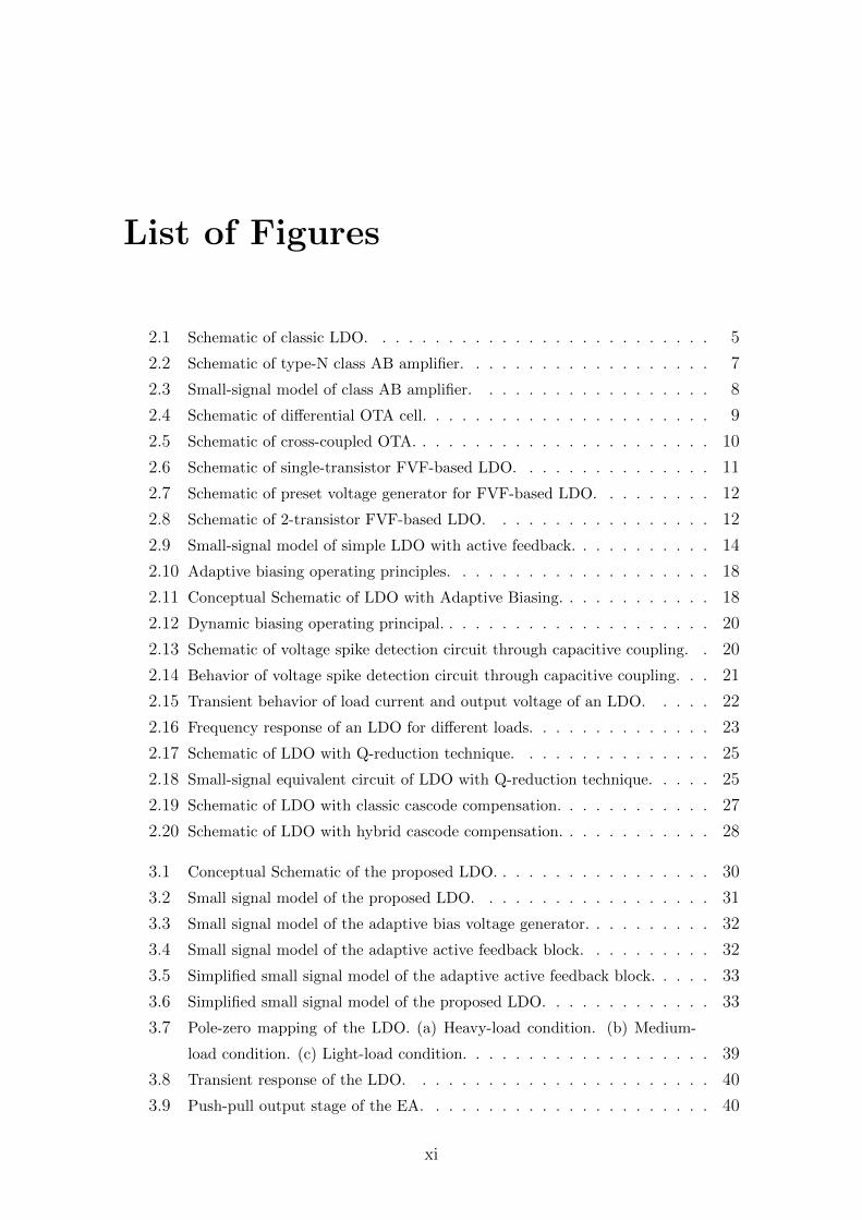
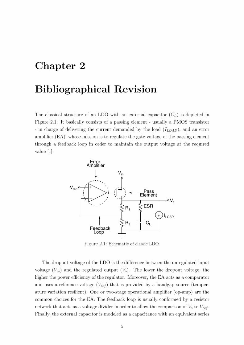
The classical structure of an LDO with an external capacitor (CL) is depicted in
Figure 2.1. It basically consists of a passing element - usually a PMOS transistor
- in charge of delivering the current demanded by the load (ILOAD), and an error
amplifier (EA), whose mission is to regulate the gate voltage of the passing element
through a feedback loop in order to maintain the output voltage at the required
value [1].
−
+
Vref
Vin
Vo
R1
R2
ESR
CL
Pass Element
FeedbackLoop
ErrorAmplifier
ILOAD
Figure 2.1: Schematic of classic LDO.
The dropout voltage of the LDO is the difference between the unregulated input
voltage (Vin) and the regulated output (Vo). The lower the dropout voltage, the
higher the power efficiency of the regulator. Moreover, the EA acts as a comparator
and uses a reference voltage (Vref ) that is provided by a bandgap source (temper-
ature variation resilient). One or two-stage operational amplifier (op-amp) are the
common choices for the EA. The feedback loop is usually conformed by a resistor
network that acts as a voltage divider in order to allow the comparison of Vo to Vref .
Finally, the external capacitor is modeled as a capacitance with an equivalent series
5
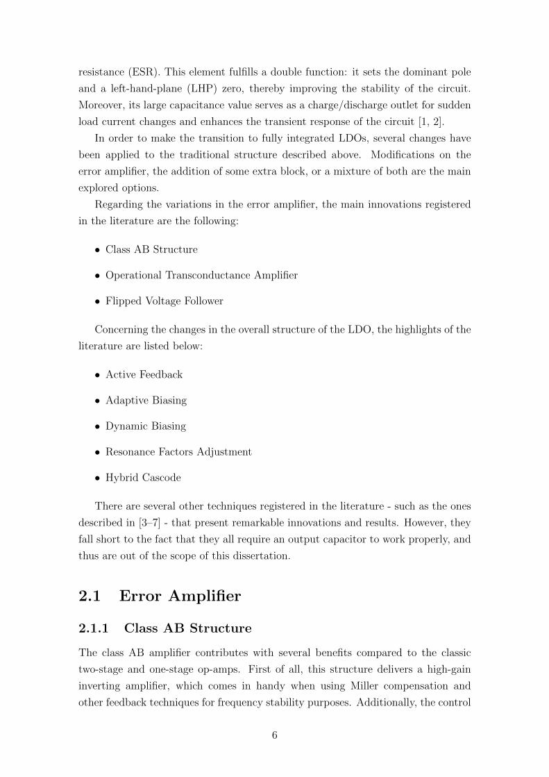
resistance (ESR). This element fulfills a double function: it sets the dominant pole
and a left-hand-plane (LHP) zero, thereby improving the stability of the circuit.
Moreover, its large capacitance value serves as a charge/discharge outlet for sudden
load current changes and enhances the transient response of the circuit [1, 2].
In order to make the transition to fully integrated LDOs, several changes have
been applied to the traditional structure described above. Modifications on the
error amplifier, the addition of some extra block, or a mixture of both are the main
explored options.
Regarding the variations in the error amplifier, the main innovations registered
in the literature are the following:
• Class AB Structure
• Operational Transconductance Amplifier
• Flipped Voltage Follower
Concerning the changes in the overall structure of the LDO, the highlights of the
literature are listed below:
• Active Feedback
• Adaptive Biasing
• Dynamic Biasing
• Resonance Factors Adjustment
• Hybrid Cascode
There are several other techniques registered in the literature - such as the ones
described in [3–7] - that present remarkable innovations and results. However, they
fall short to the fact that they all require an output capacitor to work properly, and
thus are out of the scope of this dissertation.
2.1 Error Amplifier
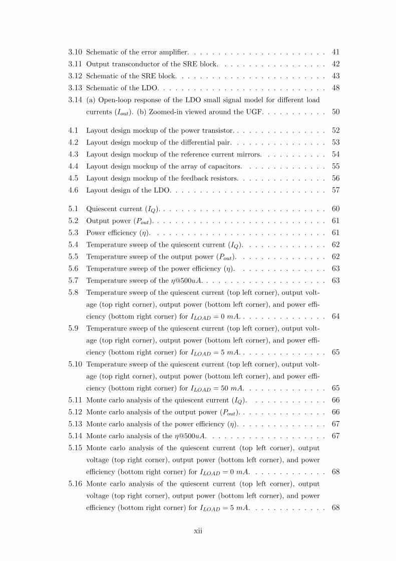
2.1.1 Class AB Structure
The class AB amplifier contributes with several benefits compared to the classic
two-stage and one-stage op-amps. First of all, this structure delivers a high-gain
inverting amplifier, which comes in handy when using Miller compensation and
other feedback techniques for frequency stability purposes. Additionally, the control
6
of the frequency poles becomes a much easier task due to the fact that the output
stage of the amplifier is semi-isolated from its input stage. The latter is a key
feature since the output stage of the amplifier will drive the power transistor of the
LDO. Hence, the speed of the LDO will be constrained by the amount of current
passing through its output stage and into/from the parasitic capacitance at the gate
of the power transistor. On top of that, the equivalent impedance of the output
stage along with the parasitic capacitance of the power transistor define one of
the frequency poles of the circuit. Therefore, the trade-off between fast transient
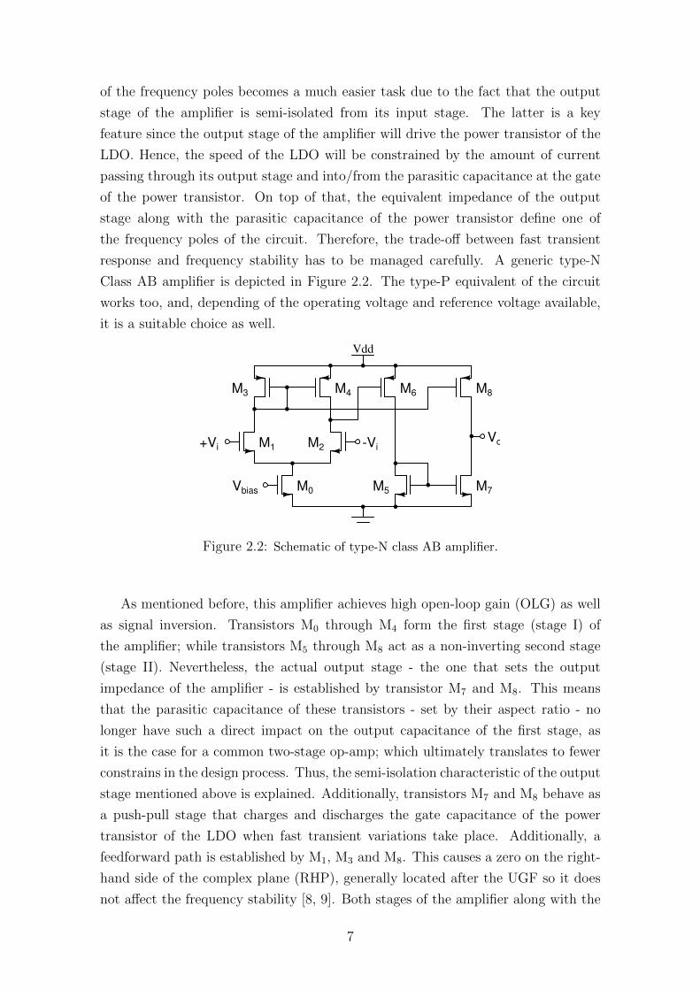
response and frequency stability has to be managed carefully. A generic type-N
Class AB amplifier is depicted in Figure 2.2. The type-P equivalent of the circuit
works too, and, depending of the operating voltage and reference voltage available,
it is a suitable choice as well.
+Vi -ViVo
Vbias
Vdd
M0
M1 M2
M3 M4 M6
M5 M7
M8
Figure 2.2: Schematic of type-N class AB amplifier.
As mentioned before, this amplifier achieves high open-loop gain (OLG) as well
as signal inversion. Transistors M0 through M4 form the first stage (stage I) of
the amplifier; while transistors M5 through M8 act as a non-inverting second stage
(stage II). Nevertheless, the actual output stage - the one that sets the output
impedance of the amplifier - is established by transistor M7 and M8. This means
that the parasitic capacitance of these transistors - set by their aspect ratio - no
longer have such a direct impact on the output capacitance of the first stage, as
it is the case for a common two-stage op-amp; which ultimately translates to fewer
constrains in the design process. Thus, the semi-isolation characteristic of the output
stage mentioned above is explained. Additionally, transistors M7 and M8 behave as
a push-pull stage that charges and discharges the gate capacitance of the power
transistor of the LDO when fast transient variations take place. Additionally, a
feedforward path is established by M1, M3 and M8. This causes a zero on the right-
hand side of the complex plane (RHP), generally located after the UGF so it does
not affect the frequency stability [8, 9]. Both stages of the amplifier along with the
7
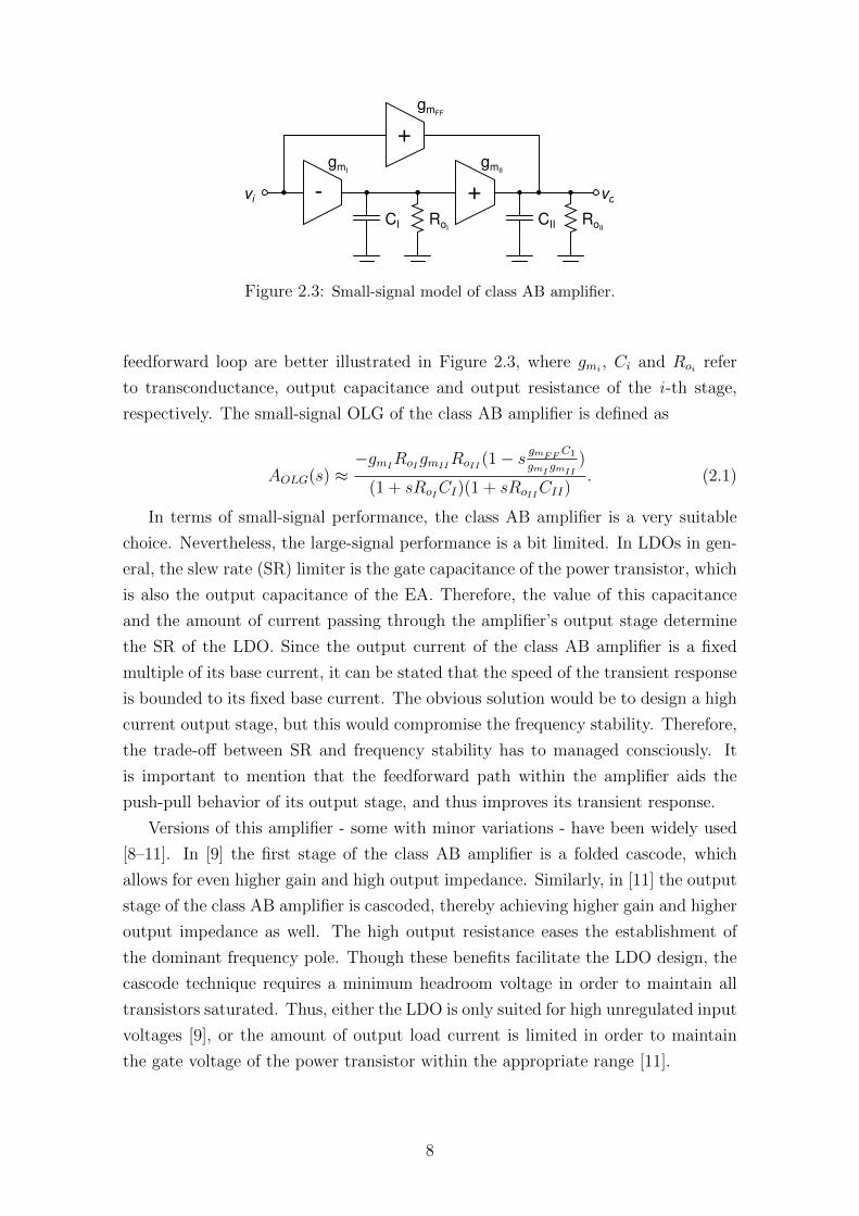
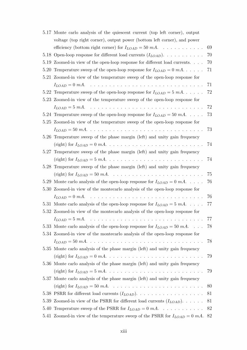
- +
gmIgmII
CI RoICII RoII
vi vo
gmFF
+
Figure 2.3: Small-signal model of class AB amplifier.
feedforward loop are better illustrated in Figure 2.3, where gmi, Ci and Roi refer
to transconductance, output capacitance and output resistance of the i -th stage,
respectively. The small-signal OLG of the class AB amplifier is defined as
AOLG(s) ≈−gmI
RoIgmIIRoII (1− s
gmFFC1
gmIgmII
)
(1 + sRoICI)(1 + sRoIICII). (2.1)
In terms of small-signal performance, the class AB amplifier is a very suitable
choice. Nevertheless, the large-signal performance is a bit limited. In LDOs in gen-
eral, the slew rate (SR) limiter is the gate capacitance of the power transistor, which
is also the output capacitance of the EA. Therefore, the value of this capacitance
and the amount of current passing through the amplifier’s output stage determine
the SR of the LDO. Since the output current of the class AB amplifier is a fixed
multiple of its base current, it can be stated that the speed of the transient response
is bounded to its fixed base current. The obvious solution would be to design a high
current output stage, but this would compromise the frequency stability. Therefore,
the trade-off between SR and frequency stability has to managed consciously. It
is important to mention that the feedforward path within the amplifier aids the
push-pull behavior of its output stage, and thus improves its transient response.
Versions of this amplifier - some with minor variations - have been widely used
[8–11]. In [9] the first stage of the class AB amplifier is a folded cascode, which
allows for even higher gain and high output impedance. Similarly, in [11] the output
stage of the class AB amplifier is cascoded, thereby achieving higher gain and higher
output impedance as well. The high output resistance eases the establishment of
the dominant frequency pole. Though these benefits facilitate the LDO design, the
cascode technique requires a minimum headroom voltage in order to maintain all
transistors saturated. Thus, either the LDO is only suited for high unregulated input
voltages [9], or the amount of output load current is limited in order to maintain
the gate voltage of the power transistor within the appropriate range [11].
8
2.1.2 Operational Transconductance Amplifier
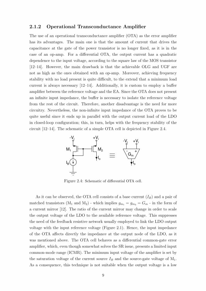
The use of an operational transconductance amplifier (OTA) as the error amplifier
has its advantages. The main one is that the amount of current that drives the
capacitance at the gate of the power transistor is no longer fixed, as it is in the
case of an op-amp. For a differential OTA, the output current has a quadratic
dependence to the input voltage, according to the square law of the MOS transistor
[12–14]. However, the main drawback is that the achievable OLG and UGF are
not as high as the ones obtained with an op-amp. Moreover, achieving frequency
stability with no load present is quite difficult, to the extend that a minimum load
current is always necessary [12–14]. Additionally, it is custom to employ a buffer
amplifier between the reference voltage and the EA. Since the OTA does not present
an infinite input impedance, the buffer is necessary to isolate the reference voltage
from the rest of the circuit. Therefore, another disadvantage is the need for more
circuitry. Nevertheless, the non-infinite input impedance of the OTA proves to be
quite useful since it ends up in parallel with the output current load of the LDO
in closed-loop configuration; this, in turn, helps with the frequency stability of the
circuit [12–14]. The schematic of a simple OTA cell is depicted in Figure 2.4.
-Vi +Vi
M1 M2
Io
IB
-Vi +Vi
Io
- +Gm
Figure 2.4: Schematic of differential OTA cell.
As it can be observed, the OTA cell consists of a base current (IB) and a pair of
matched transistors (M1 and M2) - which implies gm1 = gm2 = Gm - in the form of
a current mirror [12]. The ratio of the current mirror may change in order to scale
the output voltage of the LDO to the available reference voltage. This suppresses
the need of the feedback resistive network usually employed to link the LDO output
voltage with the input reference voltage (Figure 2.1). Hence, the input impedance
of the OTA affects directly the impedance at the output node of the LDO, as it
was mentioned above. The OTA cell behaves as a differential common-gate error
amplifier, which, even though somewhat solves the SR issue, presents a limited input
common-mode range (ICMR). The minimum input voltage of the amplifier is set by
the saturation voltage of the current source IB and the source-gate voltage of M1.
As a consequence, this technique is not suitable when the output voltage is a low
9
value (low-voltage applications) [13, 14]. After performing a small-signal analysis of
the OTA cell, the output current (Io) can be expressed as:
Io ' −Gm∆Vi. (2.2)
Furthermore, the input resistance (Ri) of the OTA cell can be defined as:
Ri ≈1
Gm
. (2.3)
In order to make the OTA equally fast to both ascending and descending tran-
sient variations of the output voltage, a cross-coupled configuration of two OTA cells
is necessary [12]. The circuit diagram is shown in Figure 2.5.
-
+
GmH
+
-
GmL
+
-
-Vi
+Vi
Io
Vdd
-Vi +Vi
VB VB Io
MH2MH1
ML1ML2
MBHMBL
M1 M2
M3 M4
M5 M6
GmLGmH
Figure 2.5: Schematic of cross-coupled OTA.
The cross-coupled OTA cells act as one single OTA that follows equations (2.2)
and (2.3) as well. In [13, 14], small changes are made to the OTA structure detailed
in [12]. In these articles, a double cross-coupled OTA configuration is used. This
means that the structure is the same as the one in Figure 2.5, except that each
internal OTA consists already of two cross-coupled OTA cells, whereas this might
seem to imply the use of more circuitry, however, each cross-coupled OTA reuses the
other one in order to optimize die area. Additionally, a current subtracter is placed
to form a positive feedback loop within the OTA. The effect of this additional block
is an overall transconductance increase, which finally translates to an OLG increase.
2.1.3 Flipped Voltage Follower
The flipped voltage follower (FVF) is a well known building block specially suited
for low-power low-voltage analog applications. The reduced output impedance due
to shunt feedback connection is the main feature of the FVF, and allows for good
10
regulation and frequency stability in LDO design [15]. Furthermore, the fact that
the core of most FVFs is one single transistor establishing a direct path between
the output and the input ensures a fast transient response. Moreover, the simplicity
of the FVF structure helps to save die area. There is one main flaw nonetheless:
the attainable OLG with the FVF is not as high as it is with other amplifiers [16].
Consequently, both load regulation and PSRR performances are degraded. The
schematic of a simple LDO using a single-transistor FVF as the EA is depicted in
Figure 2.6.
+
−
Vout
Mp
VSET
IBIAS
Vin
MC
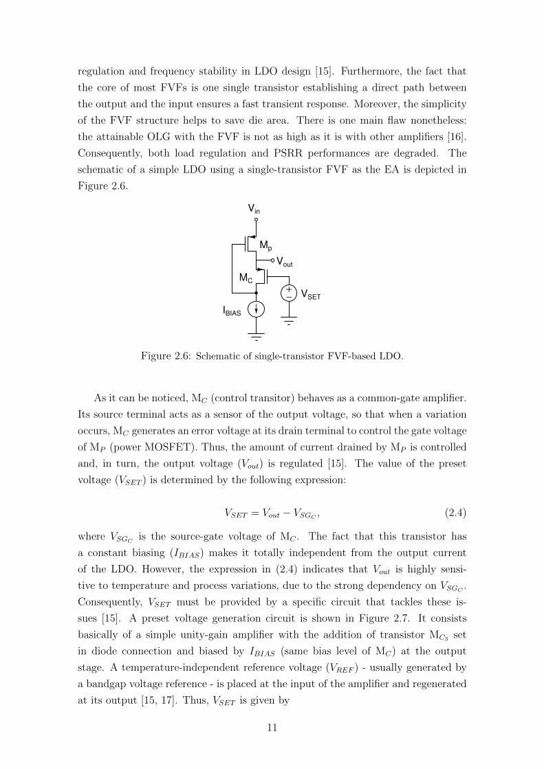
Figure 2.6: Schematic of single-transistor FVF-based LDO.
As it can be noticed, MC (control transitor) behaves as a common-gate amplifier.
Its source terminal acts as a sensor of the output voltage, so that when a variation
occurs, MC generates an error voltage at its drain terminal to control the gate voltage
of MP (power MOSFET). Thus, the amount of current drained by MP is controlled
and, in turn, the output voltage (Vout) is regulated [15]. The value of the preset
voltage (VSET ) is determined by the following expression:
VSET = Vout − VSGC, (2.4)
where VSGCis the source-gate voltage of MC . The fact that this transistor has
a constant biasing (IBIAS) makes it totally independent from the output current
of the LDO. However, the expression in (2.4) indicates that Vout is highly sensi-
tive to temperature and process variations, due to the strong dependency on VSGC.
Consequently, VSET must be provided by a specific circuit that tackles these is-
sues [15]. A preset voltage generation circuit is shown in Figure 2.7. It consists
basically of a simple unity-gain amplifier with the addition of transistor MC3 set
in diode connection and biased by IBIAS (same bias level of MC) at the output
stage. A temperature-independent reference voltage (VREF ) - usually generated by
a bandgap voltage reference - is placed at the input of the amplifier and regenerated
at its output [15, 17]. Thus, VSET is given by
11
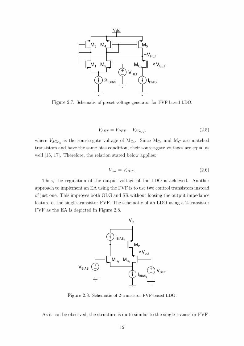
+
−
Vdd
VREF
MC3
2IBIAS
~VREF
VSETM1 M2
M3 M4 M5
IBIAS
Figure 2.7: Schematic of preset voltage generator for FVF-based LDO.
VSET = VREF − VSGC3, (2.5)
where VSGC3is the source-gate voltage of MC3 . Since MC3 and MC are matched
transistors and have the same bias condition, their source-gate voltages are equal as
well [15, 17]. Therefore, the relation stated below applies:
Vout = VREF . (2.6)
Thus, the regulation of the output voltage of the LDO is achieved. Another
approach to implement an EA using the FVF is to use two control transistors instead
of just one. This improves both OLG and SR without loosing the output impedance
feature of the single-transistor FVF. The schematic of an LDO using a 2-transistor
FVF as the EA is depicted in Figure 2.8.
+
−IBIAS2
VSET
IBIAS1
MC1MC2
MP
+
−VBIAS
Vout
Vin
Figure 2.8: Schematic of 2-transistor FVF-based LDO.
As it can be observed, the structure is quite similar to the single-transistor FVF-
12
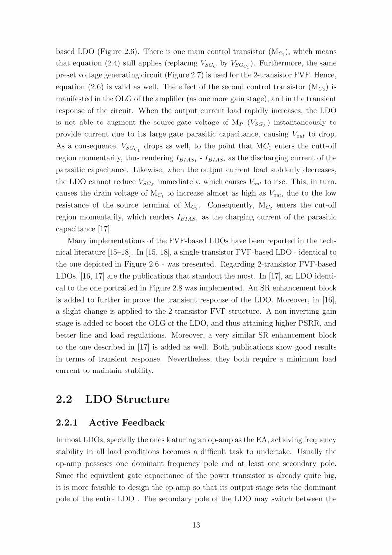
based LDO (Figure 2.6). There is one main control transistor (MC1), which means
that equation (2.4) still applies (replacing VSGCby VSGC1
). Furthermore, the same
preset voltage generating circuit (Figure 2.7) is used for the 2-transistor FVF. Hence,
equation (2.6) is valid as well. The effect of the second control transistor (MC2) is
manifested in the OLG of the amplifier (as one more gain stage), and in the transient
response of the circuit. When the output current load rapidly increases, the LDO
is not able to augment the source-gate voltage of MP (VSGP) instantaneously to
provide current due to its large gate parasitic capacitance, causing Vout to drop.
As a consequence, VSGC1drops as well, to the point that MC1 enters the cutt-off
region momentarily, thus rendering IBIAS1 - IBIAS2 as the discharging current of the
parasitic capacitance. Likewise, when the output current load suddenly decreases,
the LDO cannot reduce VSGPimmediately, which causes Vout to rise. This, in turn,
causes the drain voltage of MC1 to increase almost as high as Vout, due to the low
resistance of the source terminal of MC2 . Consequently, MC2 enters the cut-off
region momentarily, which renders IBIAS1 as the charging current of the parasitic
capacitance [17].
Many implementations of the FVF-based LDOs have been reported in the tech-
nical literature [15–18]. In [15, 18], a single-transistor FVF-based LDO - identical to
the one depicted in Figure 2.6 - was presented. Regarding 2-transistor FVF-based
LDOs, [16, 17] are the publications that standout the most. In [17], an LDO identi-
cal to the one portraited in Figure 2.8 was implemented. An SR enhancement block
is added to further improve the transient response of the LDO. Moreover, in [16],
a slight change is applied to the 2-transistor FVF structure. A non-inverting gain
stage is added to boost the OLG of the LDO, and thus attaining higher PSRR, and
better line and load regulations. Moreover, a very similar SR enhancement block
to the one described in [17] is added as well. Both publications show good results
in terms of transient response. Nevertheless, they both require a minimum load
current to maintain stability.
2.2 LDO Structure
2.2.1 Active Feedback
In most LDOs, specially the ones featuring an op-amp as the EA, achieving frequency
stability in all load conditions becomes a difficult task to undertake. Usually the
op-amp posseses one dominant frequency pole and at least one secondary pole.
Since the equivalent gate capacitance of the power transistor is already quite big,
it is more feasible to design the op-amp so that its output stage sets the dominant
pole of the entire LDO . The secondary pole of the LDO may switch between the
13
secondary pole of the op-amp and the pole generated by the output current load
and the output capacitance. Because there is no external capacitor, the output
capacitance is generated by the parasitic capacitance of the metal paths in charge of
power distribution within the integrated circuit. If designed properly, the secondary
pole of the op-amp will be located after the UGF of the LDO, and thereby will have
no effect on the stability of the system. However, the frequency pole generated by
the output current load is not fixed, and eventually falls behind the UGF as the
current load decreases, thus causing instability. The worst case takes place when no
current load is present [9, 19].
The approach of the active feedback technique is to modify and control both
the dominant and the secondary frequency pole of the LDO, through a feedback
path formed by a capacitor and a transconductor. Thus, the negative effect of the
frequency pole generated by the output current load is neutralized. Usually a LHP
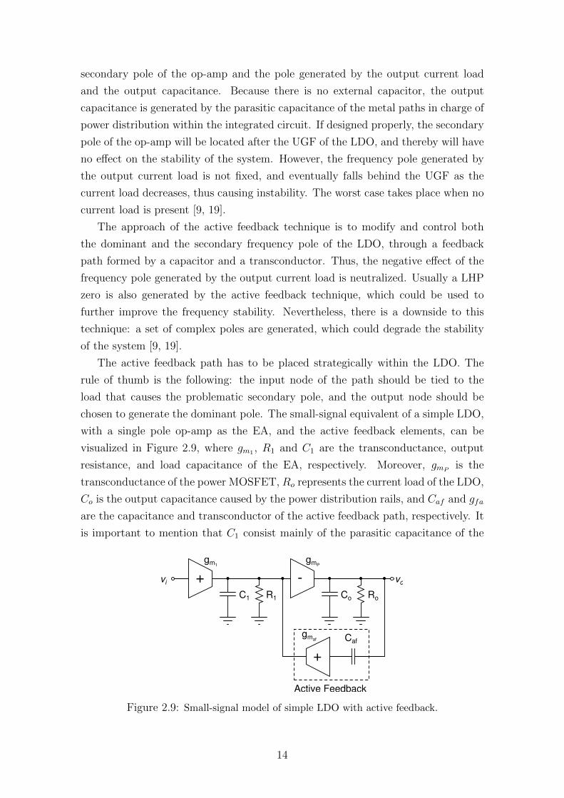
zero is also generated by the active feedback technique, which could be used to
further improve the frequency stability. Nevertheless, there is a downside to this
technique: a set of complex poles are generated, which could degrade the stability
of the system [9, 19].
The active feedback path has to be placed strategically within the LDO. The
rule of thumb is the following: the input node of the path should be tied to the
load that causes the problematic secondary pole, and the output node should be
chosen to generate the dominant pole. The small-signal equivalent of a simple LDO,
with a single pole op-amp as the EA, and the active feedback elements, can be
visualized in Figure 2.9, where gm1 , R1 and C1 are the transconductance, output
resistance, and load capacitance of the EA, respectively. Moreover, gmPis the
transconductance of the power MOSFET, Ro represents the current load of the LDO,
Co is the output capacitance caused by the power distribution rails, and Caf and gfa
are the capacitance and transconductor of the active feedback path, respectively. It
is important to mention that C1 consist mainly of the parasitic capacitance of the
gm1gmP
C1 R1 Co Ro
vi vo
gmaf
+
+ -
Caf
Active Feedback
Figure 2.9: Small-signal model of simple LDO with active feedback.
14
power MOSFET. Assuming that gmafhas an input resistance Raf , then by standard
circuit analysis methods, the transfer function is obtained as
AOLG(s) =−gm1R1gmP
Ro
(1 + sR1C1)(1 + sRoCo) + sR1[gmPRo(gmaf
RafCaf )]. (2.7)
From (2.7) another benefit of the active feedback can be noticed: the quasi-Miller
compensation using Caf . The capacitor is boosted by the gain of the power transis-
tor stage (gmPRo). However, the gain of the active feedback path (gmaf
Raf ) arises
solely from this specific configuration of its transconductor and the parallel input
resistance. Furthermore, this compensation scheme is better than the traditional
Miller because it boosts the capacitance and performs pole splitting, without gener-
ating the undesired RHP zero [19]. Assuming R1gmPRogmaf
RafCaf R1C1+RoCo,
the dominant pole (ωPdom) and the secondary pole (ωP2) can be expressed as
ωPdom∼=
1
R1[gmPRo(gmaf
RafCaf )], (2.8)
ωP2∼=gmP
(gmafRafCaf )
CoC1
. (2.9)
From (2.9) it can be noticed that the secondary pole is no longer tied to the changing
output current load, and therefore the frequency stability is ensured. However, this
analysis is assuming an ideal transconductor in the active feedback path, which is
never the case for real circuit implementation. The transconductor will cause the
appearance of a set of complex poles and this will complicate the task of achieving
stability.
LDOs using active feedback have been reported in [9, 19]. In [19], a very similar
structure to the one depicted in Figure 2.9 was used to achieve stability and to
improve the transient response of the circuit. The dominant pole is established at
the gate of the power transistor with the active feedback path, which simultaneously
provides a sensing device for the output voltage and a direct path for current charg-
ing/discharging of the gate capacitance of the power MOSFET. In [9], a slightly
different approach was taken. The active feedback was used to set the dominant
pole at the first stage of a class AB amplifier. This allowed for a higher gain due
to the quasi-Miller compensation, which reduced the size of the active feedback ca-
pacitor. Furthermore, the transconductor design was less complex, making use of
a common-gate topology instead of a common-source one (as in [19]). Both LDOs
achieved frequency stability even when no load is present, while maintaining a low
quiescent current. However, the LDO presented in [9] was able to withstand a higher
maximum current load and achieved higher OLG and UGF.
15
2.2.2 Adaptive Biasing
A fast transient response is a highly demanded feature for LDOs. The LDO must
be able to respond quickly to sudden variations of both the current load and the
unregulated power line. In general terms, the former represents a tougher challenge
than the latter, because when the current load changes, the operation region of
the power transistor changes with it. When no current load is present at all, the
power transistor is driving only the quiescent current, which is usually very small -
commonly in the range between tens and hundreds of microamperes - in order to keep
the power consumption low. Thus, the power transistor falls into the subthreshold
region, where the relationship between its source-gate voltage and its drain current
is exponential. For light loads, the power transistor will also remain in this region.
When the current load reaches a medium level, the power transistor enters the
saturation region, where the correlation between its source-gate voltage and its drain
current is quadratic. In these two regions, the transient response of the LDO is
considered quite fast, since a relatively big change in the load current translates to a
small adjustment of the gate voltage of the power MOSFET. However, when dealing
with heavy loads, the power transistor enters the linear region, and, consequently,
the dependency of the drain current towards the source-gate voltage becomes linear
as well. Therefore, an equal factor of increment in the drain current demands a larger
increment of the gate-source voltage [13, 14, 20]. As a result, the LDO transient
response becomes somewhat lethargic at the heavy-load condition, which manifests
in the output voltage as large voltage spikes with high settling times. In order to
achieve a faster response in the linear region, the LDO requires higher bandwidth
and higher SR for charging/discharging the gate capacitance of the power MOSFET
in response to the same factor of load change in the same period of time [13, 14, 20].
One logical solution to increase both bandwidth and SR is to augment the bias
current of the EA. An increment in the bias current causes a shift in the frequency
response of the amplifier, and thereby of the entire LDO. Recalling the relationship
between the drain-source resistance (rDS) and the drain current (ID) of the MOS
transistor
rDS α1
ID, (2.10)
it can be inferred that the higher the ID gets, the lower the rDS becomes. It is also
important to remember that most pole frequencies (ωp) in amplifiers are determined
by the value of rDS, since it becomes the output resistance of each stage, that is,
ωp =1
rDSCp, (2.11)
16
where Cp stands for the parasitic capacitance at the output node. Thus, a reduc-
tion in rDS translates to an increment in the pole frequency. As a consequent, an
increment in the bias current of the amplifier pushes the poles forward in the fre-
quency spectrum, thus attaining a higher bandwidth (higher UGF). Nevertheless,
this usually causes a decrease in the OLG that could degrade the performance of
the LDO. Furthermore, pushing the UGF to higher frequencies is also risky since it
gets closer to other parasitic poles and zeros of the transfer function. Ultimately,
this could reduce the phase margin (PM) and compromise the circuit stability.
Regarding the SR enhancement, it was stated before that the gate capacitance
of the power MOSFET, which is also the output capacitance of the EA, is the main
SR limiter of the LDO. So, recalling the definition of SR,
SR =IoCL
, (2.12)
where Io and CL are the output stage current and the load capacitance of the
amplifier, respectively, it is logical to infer that SR increases with the output current.
Since the output current is a fixed multiple of the bias current of the amplifier, an
increase in the latter will manifest as an increase in the former. It is important to
highlight that the expression in (2.12) only applies for amplifiers with no internal
compensation capacitor. Additionally, more bias current implies more quiescent
current, which, in turn, means more power consumption. As it can be noticed, the
trade-off between stability, SR and power consumption is very complex and probably
the most critical one in output-capacitorless LDO design.
Higher bias current appears to be a feasible solution to the transient response
issue. However, it is only necessary for heavy loads, and it would be inefficient -
and at some level even damaging - to consume more current than necessary. There-
fore, adaptive biasing is a far more efficient solution, which is to provide more bias
current only when the load demands it. There is one important disadvantage to
this technique nonetheless: once the sudden transient variation of the current load
is over, the bias current remains at its maximum value. This might not degrade
significantly the current efficiency since the load is driving a high current, but nev-
ertheless it does imply more power consumption when it is no longer needed. The
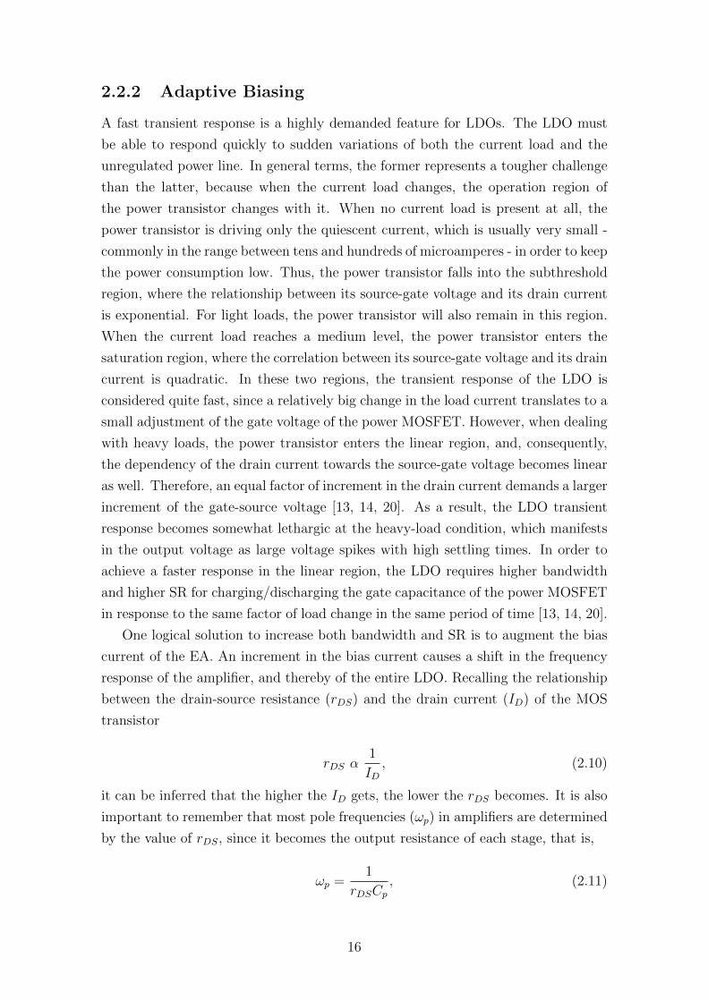
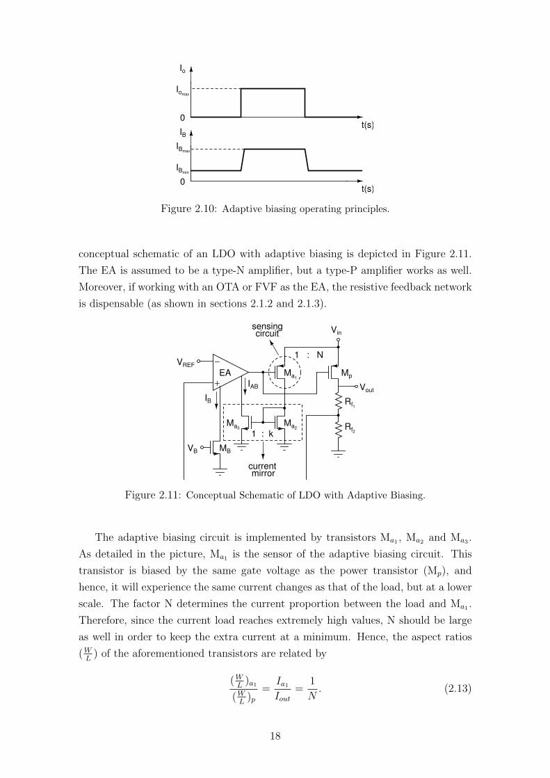
operating principles of this technique are shown in Figure 2.10.
The adaptive biasing circuit consists basically of a sensing circuit that keeps track
of the output current load, and a current mirror that provides extra bias current to
the amplifier when necessary. The sensing circuit generates a current proportional
to that of the output load, but at a much lower scale in order to maintain a decent
current efficiency. Thus, when dealing with light loads, the current sensed and
fed back to the EA by the adaptive biasing circuit is practically negligible. The
17
Iomax
0
Io
t(s)
t(s)
IBmax
IB
0
IBmin
Figure 2.10: Adaptive biasing operating principles.
conceptual schematic of an LDO with adaptive biasing is depicted in Figure 2.11.
The EA is assumed to be a type-N amplifier, but a type-P amplifier works as well.
Moreover, if working with an OTA or FVF as the EA, the resistive feedback network
is dispensable (as shown in sections 2.1.2 and 2.1.3).
−
+
VB
IB
IAB
1 : N
Mp
Rf1
Rf2
VREF
Vin
Vout
sensingcircuit
1 : k
currentmirror
EA Ma1
Ma2Ma3
MB
Figure 2.11: Conceptual Schematic of LDO with Adaptive Biasing.
The adaptive biasing circuit is implemented by transistors Ma1 , Ma2 and Ma3 .
As detailed in the picture, Ma1 is the sensor of the adaptive biasing circuit. This
transistor is biased by the same gate voltage as the power transistor (Mp), and
hence, it will experience the same current changes as that of the load, but at a lower
scale. The factor N determines the current proportion between the load and Ma1 .
Therefore, since the current load reaches extremely high values, N should be large
as well in order to keep the extra current at a minimum. Hence, the aspect ratios
(WL
) of the aforementioned transistors are related by
(WL
)a1(WL
)p=
Ia1Iout
=1
N. (2.13)
18
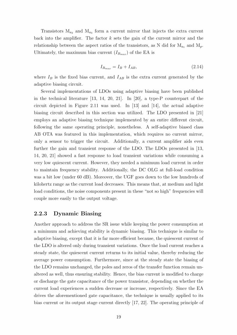
Transistors Ma2 and Ma3 form a current mirror that injects the extra current
back into the amplifier. The factor k sets the gain of the current mirror and the
relationship between the aspect ratios of the transistors, as N did for Ma1 and Mp.
Ultimately, the maximum bias current (IBmax) of the EA is
IBmax = IB + IAB, (2.14)
where IB is the fixed bias current, and IAB is the extra current generated by the
adaptive biasing circuit.
Several implementations of LDOs using adaptive biasing have been published
in the technical literature [13, 14, 20, 21]. In [20], a type-P counterpart of the
circuit depicted in Figure 2.11 was used. In [13] and [14], the actual adaptive
biasing circuit described in this section was utilized. The LDO presented in [21]
employs an adaptive biasing technique implemented by an entire different circuit,
following the same operating principle, nonetheless. A self-adaptive biased class
AB OTA was featured in this implementation, which requires no current mirror,
only a sensor to trigger the circuit. Additionally, a current amplifier aids even
further the gain and transient response of the LDO. The LDOs presented in [13,
14, 20, 21] showed a fast response to load transient variations while consuming a
very low quiescent current. However, they needed a minimum load current in order
to maintain frequency stability. Additionally, the DC OLG at full-load condition
was a bit low (under 60 dB). Moreover, the UGF goes down to the low hundreds of
kilohertz range as the current load decreases. This means that, at medium and light
load conditions, the noise components present in these “not so high” frequencies will
couple more easily to the output voltage.
2.2.3 Dynamic Biasing
Another approach to address the SR issue while keeping the power consumption at
a minimum and achieving stability is dynamic biasing. This technique is similar to
adaptive biasing, except that it is far more efficient because, the quiescent current of
the LDO is altered only during transient variations. Once the load current reaches a
steady state, the quiescent current returns to its initial value, thereby reducing the
average power consumption. Furthermore, since at the steady state the biasing of
the LDO remains unchanged, the poles and zeros of the transfer function remain un-
altered as well, thus ensuring stability. Hence, the bias current is modified to charge
or discharge the gate capacitance of the power transistor, depending on whether the
current load experiences a sudden decrease or increase, respectively. Since the EA
drives the aforementioned gate capacitance, the technique is usually applied to its
bias current or its output stage current directly [17, 22]. The operating principle of
19
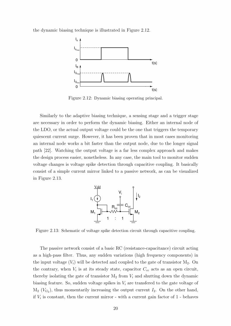
the dynamic biasing technique is illustrated in Figure 2.12.
Iomax
0
Io
t(s)
t(s)
IQmax
IB
0
IQmin
Figure 2.12: Dynamic biasing operating principal.
Similarly to the adaptive biasing technique, a sensing stage and a trigger stage
are necessary in order to perform the dynamic biasing. Either an internal node of
the LDO, or the actual output voltage could be the one that triggers the temporary
quiescent current surge. However, it has been proven that in most cases monitoring
an internal node works a bit faster than the output node, due to the longer signal
path [22]. Watching the output voltage is a far less complex approach and makes
the design process easier, nonetheless. In any case, the main tool to monitor sudden
voltage changes is voltage spike detection through capacitive coupling. It basically
consist of a simple current mirror linked to a passive network, as can be visualized
in Figure 2.13.
Vdd
Vi
I1
I2
RccCcc
M1 M2
1 : 1
Figure 2.13: Schematic of voltage spike detection circuit through capacitive coupling.
The passive network consist of a basic RC (resistance-capacitance) circuit acting
as a high-pass filter. Thus, any sudden variations (high frequency components) in
the input voltage (Vi) will be detected and coupled to the gate of transistor M2. On
the contrary, when Vi is at its steady state, capacitor Ccc acts as an open circuit,
thereby isolating the gate of transistor M2 from Vi and shutting down the dynamic
biasing feature. So, sudden voltage spikes in Vi are transfered to the gate voltage of
M2 (VG2), thus momentarily increasing the output current I2. On the other hand,
if Vi is constant, then the current mirror - with a current gain factor of 1 - behaves
20
normally, thereby yielding I1 = I2 [17]. The behavior of the voltage spike detection
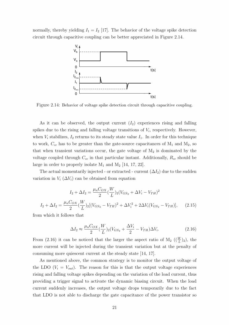
circuit through capacitive coupling can be better appreciated in Figure 2.14.
Va
0
Vi
t(s)
t(s)
I2max
I2
0
I2min
Vb
I1
Figure 2.14: Behavior of voltage spike detection circuit through capacitive coupling.
As it can be observed, the output current (I2) experiences rising and falling
spikes due to the rising and falling voltage transitions of Vi, respectively. However,
when Vi stabilizes, I2 returns to its steady state value I1. In order for this technique
to work, Ccc has to be greater than the gate-source capacitances of M1 and M2, so
that when transient variations occur, the gate voltage of M2 is dominated by the
voltage coupled through Ccc in that particular instant. Additionally, Rcc should be
large in order to properly isolate M1 and M2 [14, 17, 22].
The actual momentarily injected - or extracted - current (∆I2) due to the sudden
variation in Vi (∆Vi) can be obtained from equation
I2 + ∆I2 =µnCOX
2(W
L)2(VGS2 + ∆Vi − VTH)2
I2 + ∆I2 =µnCOX
2(W
L)2[(VGS2 − VTH)2 + ∆V 2
i + 2∆Vi(VGS2 − VTH)], (2.15)
from which it follows that
∆I2 ≈µnCOX
2(W
L)2(VGS2 +
∆Vi2− VTH)∆Vi. (2.16)
From (2.16) it can be noticed that the larger the aspect ratio of M2 ((WL
)2), the
more current will be injected during the transient variation but at the penalty of
consuming more quiescent current at the steady state [14, 17].
As mentioned above, the common strategy is to monitor the output voltage of
the LDO (Vi = Vout). The reason for this is that the output voltage experiences
rising and falling voltage spikes depending on the variation of the load current, thus
providing a trigger signal to activate the dynamic biasing circuit. When the load
current suddenly increases, the output voltage drops temporarily due to the fact
that LDO is not able to discharge the gate capacitance of the power transistor so
21
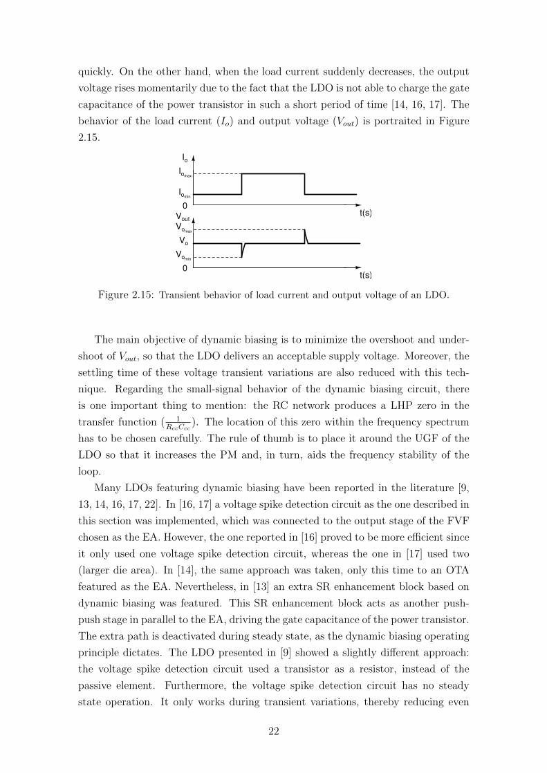
quickly. On the other hand, when the load current suddenly decreases, the output
voltage rises momentarily due to the fact that the LDO is not able to charge the gate
capacitance of the power transistor in such a short period of time [14, 16, 17]. The
behavior of the load current (Io) and output voltage (Vout) is portraited in Figure
2.15.
0
Io
t(s)
t(s)
Vomax
Vout
0
Vomin
Iomax
Vo
Iomin
Figure 2.15: Transient behavior of load current and output voltage of an LDO.
The main objective of dynamic biasing is to minimize the overshoot and under-
shoot of Vout, so that the LDO delivers an acceptable supply voltage. Moreover, the
settling time of these voltage transient variations are also reduced with this tech-
nique. Regarding the small-signal behavior of the dynamic biasing circuit, there
is one important thing to mention: the RC network produces a LHP zero in the
transfer function ( 1RccCcc
). The location of this zero within the frequency spectrum
has to be chosen carefully. The rule of thumb is to place it around the UGF of the
LDO so that it increases the PM and, in turn, aids the frequency stability of the
loop.
Many LDOs featuring dynamic biasing have been reported in the literature [9,
13, 14, 16, 17, 22]. In [16, 17] a voltage spike detection circuit as the one described in
this section was implemented, which was connected to the output stage of the FVF
chosen as the EA. However, the one reported in [16] proved to be more efficient since
it only used one voltage spike detection circuit, whereas the one in [17] used two
(larger die area). In [14], the same approach was taken, only this time to an OTA
featured as the EA. Nevertheless, in [13] an extra SR enhancement block based on
dynamic biasing was featured. This SR enhancement block acts as another push-
push stage in parallel to the EA, driving the gate capacitance of the power transistor.
The extra path is deactivated during steady state, as the dynamic biasing operating
principle dictates. The LDO presented in [9] showed a slightly different approach:
the voltage spike detection circuit used a transistor as a resistor, instead of the
passive element. Furthermore, the voltage spike detection circuit has no steady
state operation. It only works during transient variations, thereby reducing even
22
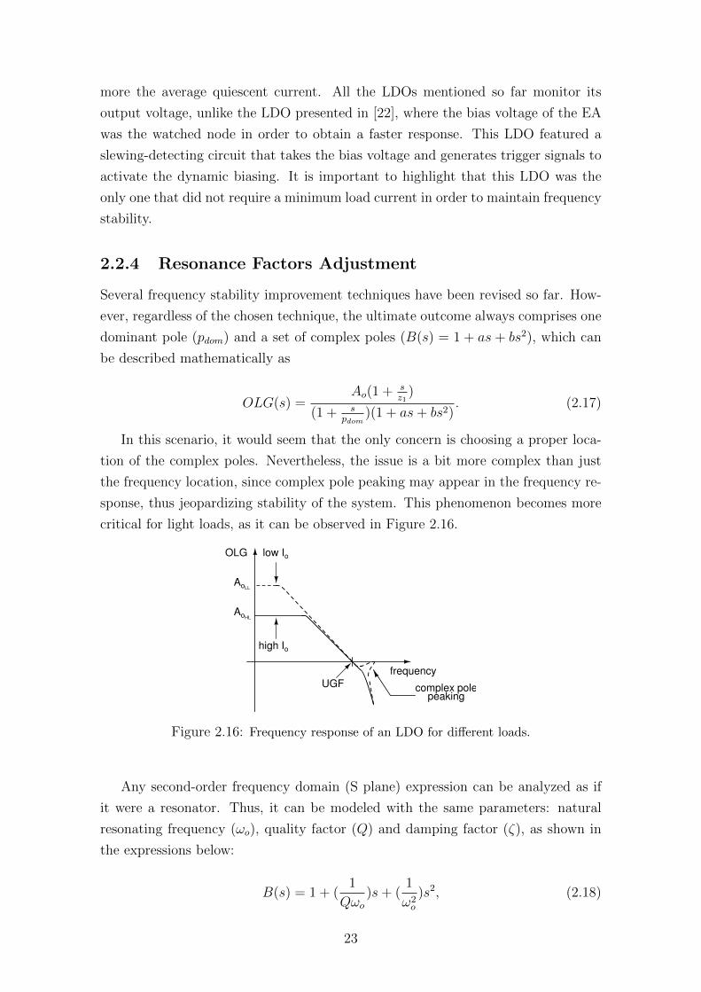
more the average quiescent current. All the LDOs mentioned so far monitor its
output voltage, unlike the LDO presented in [22], where the bias voltage of the EA
was the watched node in order to obtain a faster response. This LDO featured a
slewing-detecting circuit that takes the bias voltage and generates trigger signals to
activate the dynamic biasing. It is important to highlight that this LDO was the
only one that did not require a minimum load current in order to maintain frequency
stability.
2.2.4 Resonance Factors Adjustment
Several frequency stability improvement techniques have been revised so far. How-
ever, regardless of the chosen technique, the ultimate outcome always comprises one
dominant pole (pdom) and a set of complex poles (B(s) = 1 + as + bs2), which can
be described mathematically as
OLG(s) =Ao(1 + s
z1)
(1 + spdom
)(1 + as+ bs2). (2.17)
In this scenario, it would seem that the only concern is choosing a proper loca-
tion of the complex poles. Nevertheless, the issue is a bit more complex than just
the frequency location, since complex pole peaking may appear in the frequency re-
sponse, thus jeopardizing stability of the system. This phenomenon becomes more
critical for light loads, as it can be observed in Figure 2.16.
OLG
frequency
complex polepeaking
low Io
high Io
AoLL
AoHL
UGF
Figure 2.16: Frequency response of an LDO for different loads.
Any second-order frequency domain (S plane) expression can be analyzed as if
it were a resonator. Thus, it can be modeled with the same parameters: natural
resonating frequency (ωo), quality factor (Q) and damping factor (ζ), as shown in
the expressions below:
B(s) = 1 + (1
Qωo)s+ (
1
ω2o
)s2, (2.18)
23
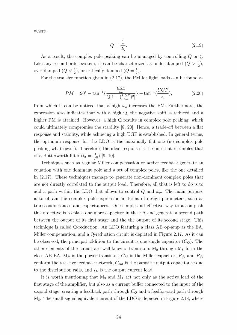
where
Q =1
2ζ. (2.19)
As a result, the complex pole peaking can be managed by controlling Q or ζ.
Like any second-order system, it can be characterized as under-damped (Q > 12),
over-damped (Q < 12), or critically damped (Q = 1
2).
For the transfer function given in (2.17), the PM for light loads can be found as
PM = 90 − tan−1UGFωo
Q[1− (UGFωo
)2]+ tan−1(
UGF
z1), (2.20)
from which it can be noticed that a high ωo increases the PM. Furthermore, the
expression also indicates that with a high Q, the negative shift is reduced and a
higher PM is attained. However, a high Q results in complex pole peaking, which
could ultimately compromise the stability [8, 20]. Hence, a trade-off between a flat
response and stability, while achieving a high UGF is established. In general terms,
the optimum response for the LDO is the maximally flat one (no complex pole
peaking whatsoever). Therefore, the ideal response is the one that resembles that
of a Butterworth filter (Q = 1√2) [9, 10].
Techniques such as regular Miller compensation or active feedback generate an
equation with one dominant pole and a set of complex poles, like the one detailed
in (2.17). These techniques manage to generate non-dominant complex poles that
are not directly correlated to the output load. Therefore, all that is left to do is to
add a path within the LDO that allows to control Q and ωo. The main purpose
is to obtain the complex pole expression in terms of design parameters, such as
transconductances and capacitances. One simple and effective way to accomplish
this objective is to place one more capacitor in the EA and generate a second path
between the output of its first stage and the the output of its second stage. This
technique is called Q-reduction. An LDO featuring a class AB op-amp as the EA,
Miller compensation, and a Q-reduction circuit is depicted in Figure 2.17. As it can
be observed, the principal addition to the circuit is one single capacitor (CQ). The
other elements of the circuit are well-known: transistors M0 through M8 form the
class AB EA, MP is the power transistor, CM is the Miller capacitor, Rf1 and Rf2
conform the resistive feedback network, Cout is the parasitic output capacitance due
to the distribution rails, and IL is the output current load.
It is worth mentioning that M3 and M4 act not only as the active load of the
first stage of the amplifier, but also as a current buffer connected to the input of the
second stage, creating a feedback path through CQ and a feedforward path through
M8. The small-signal equivalent circuit of the LDO is depicted in Figure 2.18, where
24
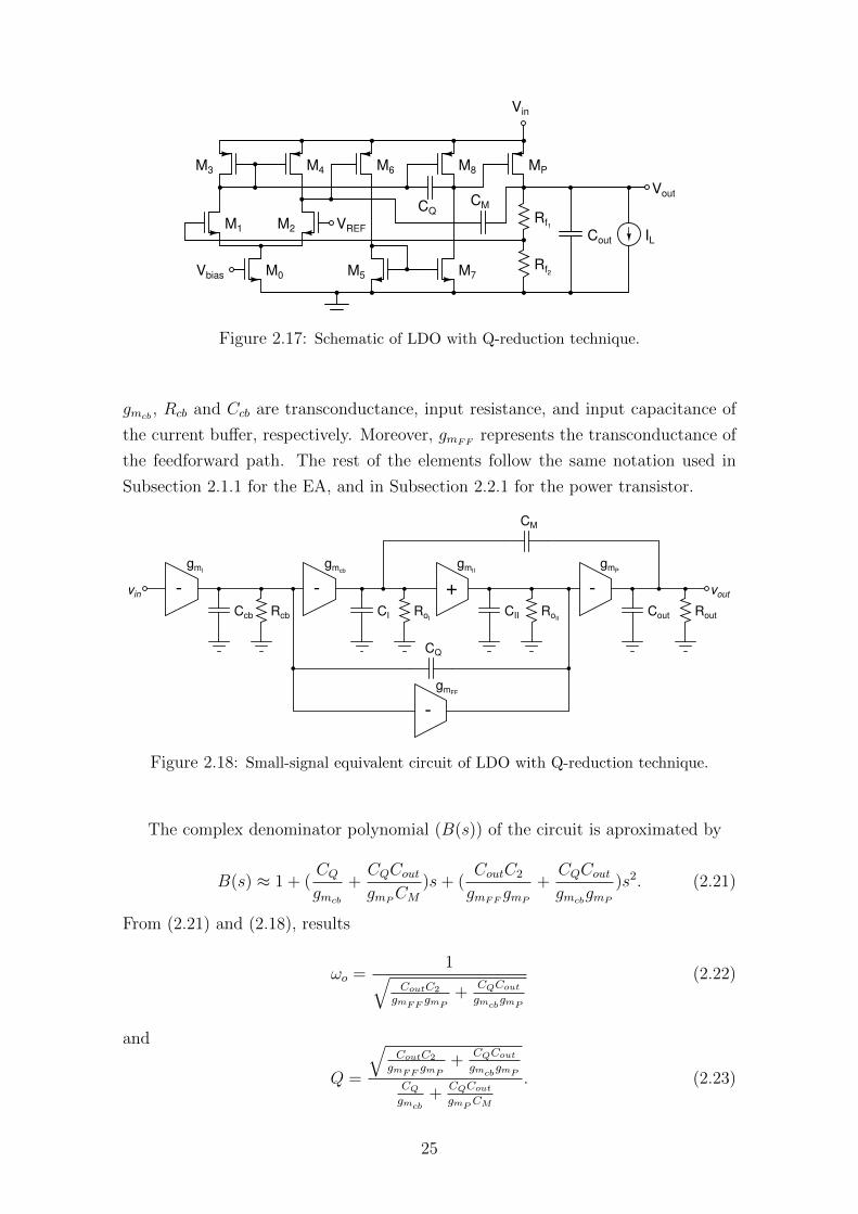
VREF
Vout
Vbias M0
M1 M2
M3 M4 M6
M5 M7
M8
Vin
CQ
MP
Rf1
Rf2
Cout IL
CM
Figure 2.17: Schematic of LDO with Q-reduction technique.
gmcb, Rcb and Ccb are transconductance, input resistance, and input capacitance of
the current buffer, respectively. Moreover, gmFFrepresents the transconductance of
the feedforward path. The rest of the elements follow the same notation used in
Subsection 2.1.1 for the EA, and in Subsection 2.2.1 for the power transistor.
- +
gmIgmII
Ccb Rcb CII RoII
vin vout-
gmcb
CI RoI
-
gmP
Cout Rout
-
gmFF
CQ
CM
Figure 2.18: Small-signal equivalent circuit of LDO with Q-reduction technique.
The complex denominator polynomial (B(s)) of the circuit is aproximated by
B(s) ≈ 1 + (CQgmcb
+CQCoutgmP
CM)s+ (
CoutC2
gmFFgmP
+CQCoutgmcb
gmP
)s2. (2.21)
From (2.21) and (2.18), results
ωo =1√
CoutC2
gmFFgmP
+CQCout
gmcbgmP
(2.22)
and
Q =
√CoutC2
gmFFgmP
+CQCout
gmcbgmP
CQ
gmcb+
CQCout
gmPCM
. (2.23)
25
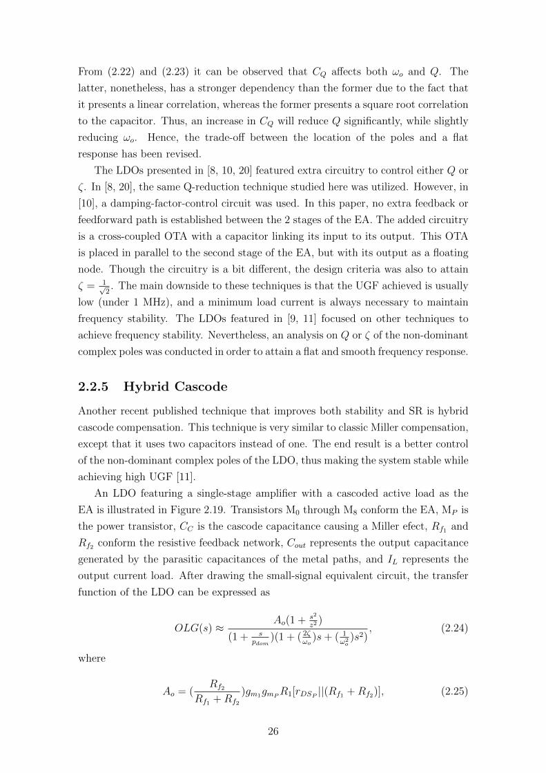
From (2.22) and (2.23) it can be observed that CQ affects both ωo and Q. The
latter, nonetheless, has a stronger dependency than the former due to the fact that
it presents a linear correlation, whereas the former presents a square root correlation
to the capacitor. Thus, an increase in CQ will reduce Q significantly, while slightly
reducing ωo. Hence, the trade-off between the location of the poles and a flat
response has been revised.
The LDOs presented in [8, 10, 20] featured extra circuitry to control either Q or
ζ. In [8, 20], the same Q-reduction technique studied here was utilized. However, in
[10], a damping-factor-control circuit was used. In this paper, no extra feedback or
feedforward path is established between the 2 stages of the EA. The added circuitry
is a cross-coupled OTA with a capacitor linking its input to its output. This OTA
is placed in parallel to the second stage of the EA, but with its output as a floating
node. Though the circuitry is a bit different, the design criteria was also to attain
ζ = 1√2. The main downside to these techniques is that the UGF achieved is usually
low (under 1 MHz), and a minimum load current is always necessary to maintain
frequency stability. The LDOs featured in [9, 11] focused on other techniques to
achieve frequency stability. Nevertheless, an analysis on Q or ζ of the non-dominant
complex poles was conducted in order to attain a flat and smooth frequency response.
2.2.5 Hybrid Cascode
Another recent published technique that improves both stability and SR is hybrid
cascode compensation. This technique is very similar to classic Miller compensation,
except that it uses two capacitors instead of one. The end result is a better control
of the non-dominant complex poles of the LDO, thus making the system stable while
achieving high UGF [11].
An LDO featuring a single-stage amplifier with a cascoded active load as the
EA is illustrated in Figure 2.19. Transistors M0 through M8 conform the EA, MP is
the power transistor, CC is the cascode capacitance causing a Miller efect, Rf1 and
Rf2 conform the resistive feedback network, Cout represents the output capacitance
generated by the parasitic capacitances of the metal paths, and IL represents the
output current load. After drawing the small-signal equivalent circuit, the transfer
function of the LDO can be expressed as
OLG(s) ≈Ao(1 + s2
z2)
(1 + spdom
)(1 + ( 2ζωo
)s+ ( 1ω2o)s2)
, (2.24)
where
Ao = (Rf2
Rf1 +Rf2
)gm1gmPR1[rDSP
||(Rf1 +Rf2)], (2.25)
26
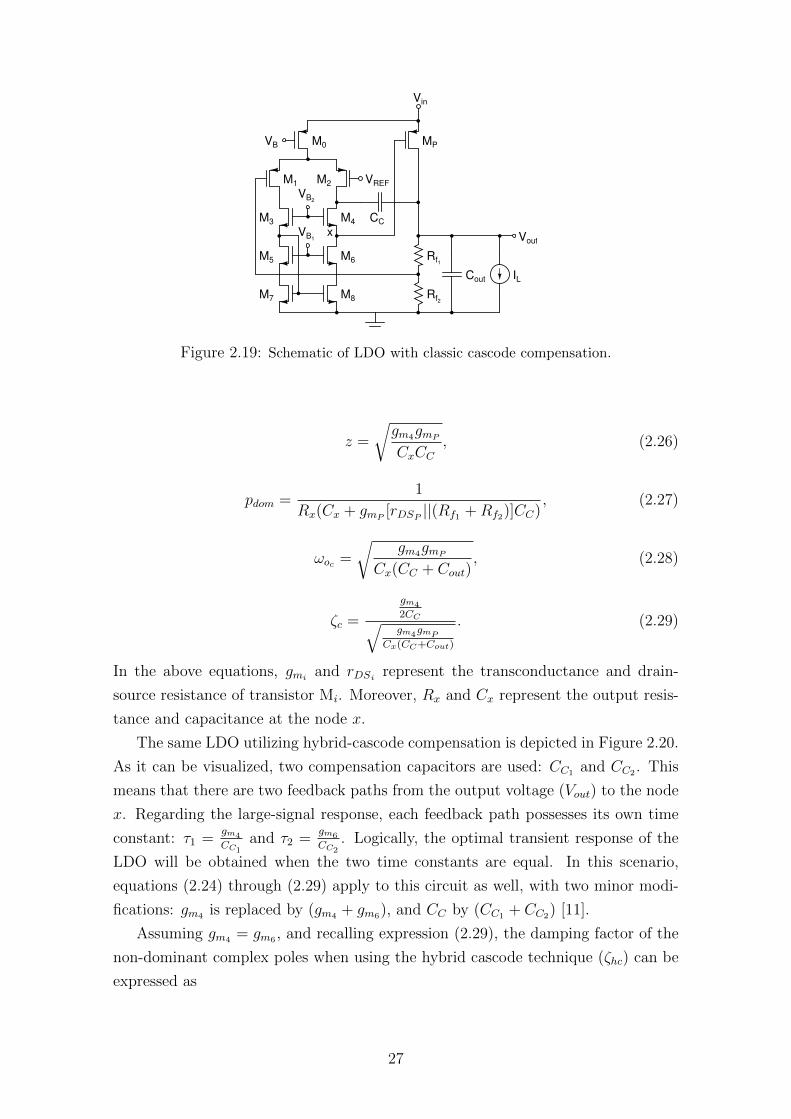
CC
VREF
Rf1
Rf2
Cout IL
VB M0 MP
M1 M2
M3 M4
M5 M6
M7 M8
VB1
VB2
Vin
Voutx
Figure 2.19: Schematic of LDO with classic cascode compensation.
z =
√gm4gmP
CxCC, (2.26)
pdom =1
Rx(Cx + gmP[rDSP
||(Rf1 +Rf2)]CC), (2.27)
ωoc =
√gm4gmP
Cx(CC + Cout), (2.28)
ζc =
gm4
2CC√gm4gmP
Cx(CC+Cout)
. (2.29)
In the above equations, gmiand rDSi
represent the transconductance and drain-
source resistance of transistor Mi. Moreover, Rx and Cx represent the output resis-
tance and capacitance at the node x.
The same LDO utilizing hybrid-cascode compensation is depicted in Figure 2.20.
As it can be visualized, two compensation capacitors are used: CC1 and CC2 . This
means that there are two feedback paths from the output voltage (Vout) to the node
x. Regarding the large-signal response, each feedback path possesses its own time
constant: τ1 =gm4
CC1and τ2 =
gm6
CC2. Logically, the optimal transient response of the
LDO will be obtained when the two time constants are equal. In this scenario,
equations (2.24) through (2.29) apply to this circuit as well, with two minor modi-
fications: gm4 is replaced by (gm4 + gm6), and CC by (CC1 + CC2) [11].
Assuming gm4 = gm6 , and recalling expression (2.29), the damping factor of the
non-dominant complex poles when using the hybrid cascode technique (ζhc) can be
expressed as
27
CC1
VREF
Rf1
Rf2
Cout IL
VB M0 MP
M1 M2
M3 M4
M5 M6
M7 M8
VB1
VB2
Vin
Voutx
CC2
Figure 2.20: Schematic of LDO with hybrid cascode compensation.
ζhc =
(gm4+gm6 )
2CC√gm4gmP
Cx(CC+Cout)
=
gm4
CC√gm4gmP
Cx(CC+Cout)
= 2ζc. (2.30)
Similarly, recalling (2.28), the frequency of the non-dominant complex poles when
using hybrid cascode compensation (ωohc) is
ωohc =
√(gm4 + gm6)gmP
Cx(CC + Cout)=√
2ωoc . (2.31)
From (2.30) it can be deduced that the hybrid cascode technique attains a much
flatter and smoother frequency response than does the classic cascode, using the
same resources (die area, power consumption). Likewise, from (2.31) it can be
noticed that hybrid cascode compensation allocates the non-dominant complex poles
at higher frequencies than those of the classic cascode compensation. As mentioned
above, another benefit of this technique is that it presents a balanced transient
response. The premise that states the time constants are equal (τ1 = τ2) forces
the circuit to respond equally fast to both sudden increase and decrease of the load
current [11]. There is one downside to this approach: cascode technique always
represents a challenge to low-voltage applications due to the minimum headroom
required to maintain all transistors in the saturation region.
The hybrid cascode technique was presented in [11]. The LDO in this article
achieved both high OLG and high UGF. However, the maximum current load sup-
ported was somewhat small due to the headroom limitation of the hybrid cascode
technique. Moreover, the quiescent current of the circuit was a bit high. The LDO
proved to be stable for all load conditions.
28
Chapter 3
Schematic Design
From all the techniques and topologies studied in Chapter 2, only three were chosen
to implement the LDO. The final selection comprised active feedback, dynamic
biasing, and a class AB op-amp as the EA. Furthermore, some innovations were
implemented, such as the adaptive (load-dependent) and temperature resilient active
feedback compensation scheme. Throughout this chapter a more thorough analysis
of the LDO architecture will be presented. First, the proposed LDO structure will
be introduced. Then, a closer look at the behavior of the circuit in both frequency
and time domain will be taken. Next, the circuit implementation - including full
transistor dimensioning - along with some design criteria will be described. Finally,
the results of several simulations will be shown in order to verify the performance
of the LDO schematic design.
3.1 LDO Structure
Figure 3.1 illustrates the structure of the proposed LDO. The main classic elements
can be visualized: the power transistor (MP ), the EA, the resistive feedback network
(Rf1 and Rf2), the output capacitance generated by the power distribution metal
paths (Cout), and the output current load (ILOAD). The additional blocks can be
easily noticed as well: the Miller compensation capacitor (Cm), the adaptive active
feedback path (Ca, Gma andGmb), the dynamic biasing feedback path (Ccc andGmf
),
and the slew rate enhancement (SRE) path (Ccc and Gmx). A high-speed loop is
generated by Gma and Gmf. These two paths implement a fast push-pull network
that charges and discharges the gate capacitance of MP . Additionally, another high-
speed loop is established by Gmx , which is only activated during transient variations
and thereby has no effect on the steady-state response of the circuit. Hence, the LDO
response time is reduced even more while keeping the average power consumption
at a minimum. Moreover, due to its null steady-state operation, accuracy is not
a requirement for this high-speed loop. The steady line and load regulation are
29
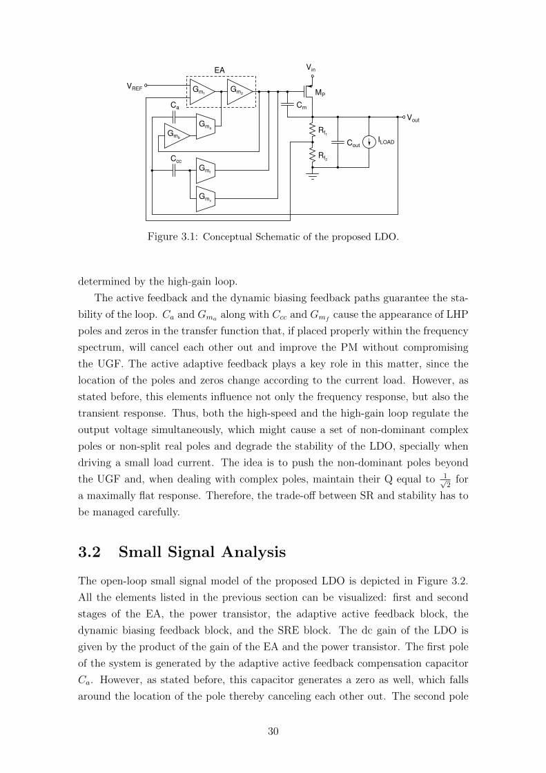
Rf1
Rf2
CoutILOAD
Gm1Gm2
Gma
Gmf
Gmx
Ca
Ccc
Cm
VREF
Vout
VinEA
MP
Gmb
Figure 3.1: Conceptual Schematic of the proposed LDO.
determined by the high-gain loop.
The active feedback and the dynamic biasing feedback paths guarantee the sta-
bility of the loop. Ca and Gma along with Ccc and Gmfcause the appearance of LHP
poles and zeros in the transfer function that, if placed properly within the frequency
spectrum, will cancel each other out and improve the PM without compromising
the UGF. The active adaptive feedback plays a key role in this matter, since the
location of the poles and zeros change according to the current load. However, as
stated before, this elements influence not only the frequency response, but also the
transient response. Thus, both the high-speed and the high-gain loop regulate the
output voltage simultaneously, which might cause a set of non-dominant complex
poles or non-split real poles and degrade the stability of the LDO, specially when
driving a small load current. The idea is to push the non-dominant poles beyond
the UGF and, when dealing with complex poles, maintain their Q equal to 1√2
for
a maximally flat response. Therefore, the trade-off between SR and stability has to
be managed carefully.
3.2 Small Signal Analysis
The open-loop small signal model of the proposed LDO is depicted in Figure 3.2.
All the elements listed in the previous section can be visualized: first and second
stages of the EA, the power transistor, the adaptive active feedback block, the
dynamic biasing feedback block, and the SRE block. The dc gain of the LDO is
given by the product of the gain of the EA and the power transistor. The first pole
of the system is generated by the adaptive active feedback compensation capacitor
Ca. However, as stated before, this capacitor generates a zero as well, which falls
around the location of the pole thereby canceling each other out. The second pole
30
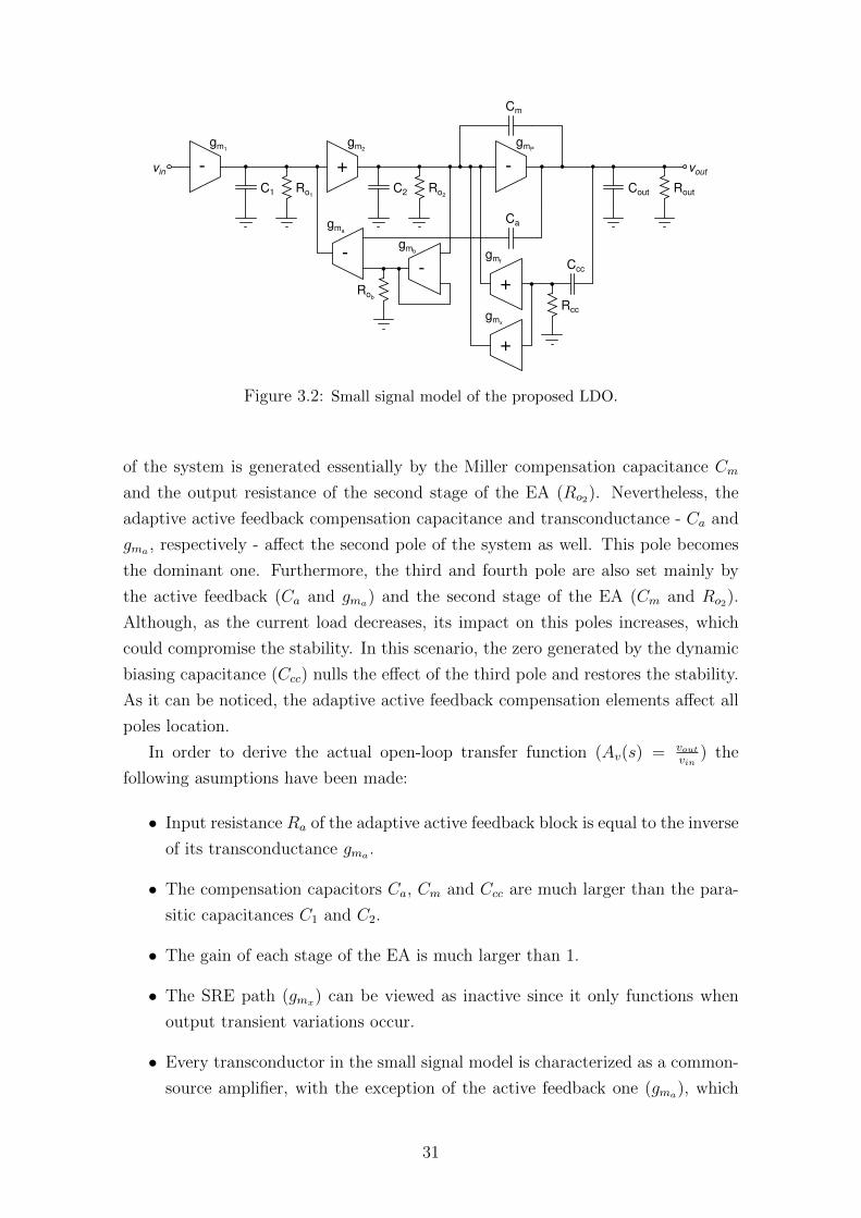
+
gm2
C2 Ro2
vin vout-
gm1
C1 Ro1
-
gmP
Cout Rout
Ca
Cm
gma
-
gmb
Rob
Ccc
Rcc
+
gmf
+
gmx
-
Figure 3.2: Small signal model of the proposed LDO.
of the system is generated essentially by the Miller compensation capacitance Cm
and the output resistance of the second stage of the EA (Ro2). Nevertheless, the
adaptive active feedback compensation capacitance and transconductance - Ca and
gma , respectively - affect the second pole of the system as well. This pole becomes
the dominant one. Furthermore, the third and fourth pole are also set mainly by
the active feedback (Ca and gma) and the second stage of the EA (Cm and Ro2).
Although, as the current load decreases, its impact on this poles increases, which
could compromise the stability. In this scenario, the zero generated by the dynamic
biasing capacitance (Ccc) nulls the effect of the third pole and restores the stability.
As it can be noticed, the adaptive active feedback compensation elements affect all
poles location.
In order to derive the actual open-loop transfer function (Av(s) = voutvin
) the
following asumptions have been made:
• Input resistance Ra of the adaptive active feedback block is equal to the inverse
of its transconductance gma .
• The compensation capacitors Ca, Cm and Ccc are much larger than the para-
sitic capacitances C1 and C2.
• The gain of each stage of the EA is much larger than 1.
• The SRE path (gmx) can be viewed as inactive since it only functions when
output transient variations occur.
• Every transconductor in the small signal model is characterized as a common-
source amplifier, with the exception of the active feedback one (gma), which
31
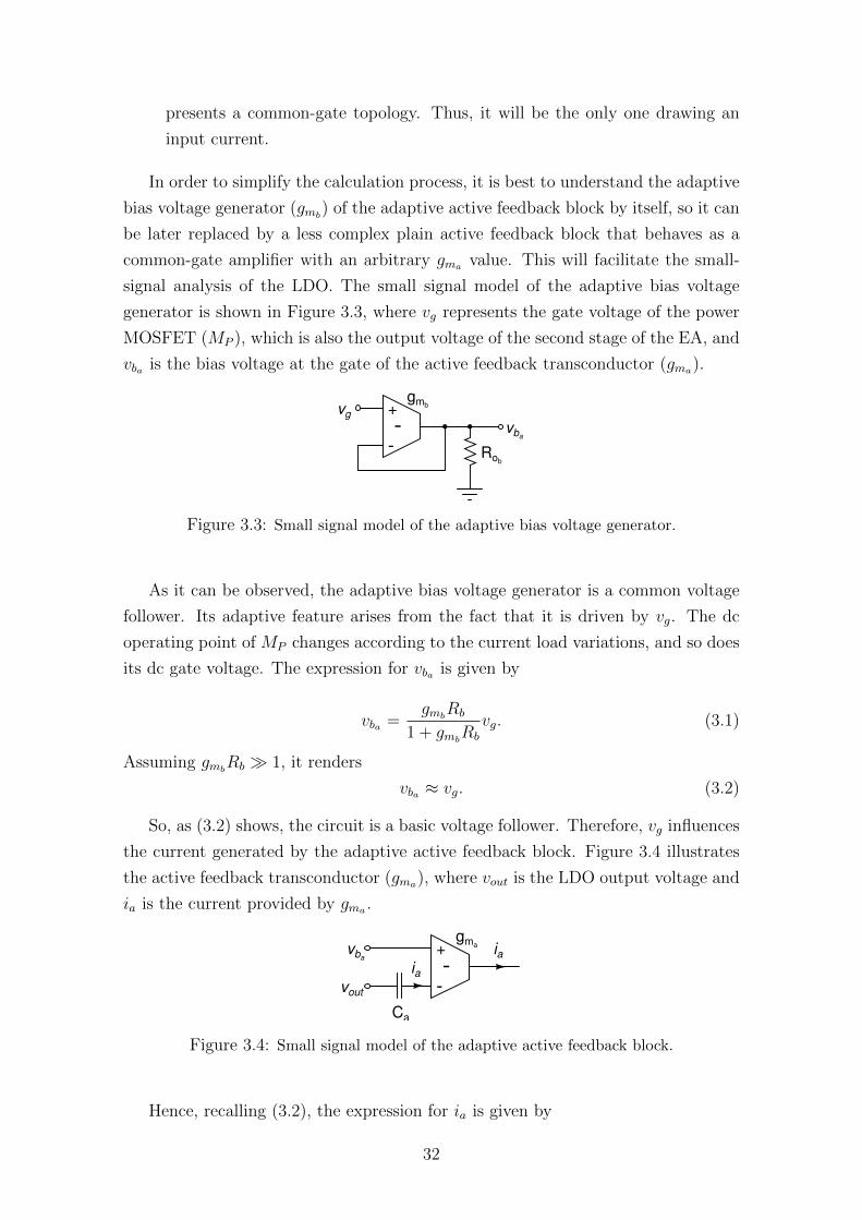
presents a common-gate topology. Thus, it will be the only one drawing an
input current.
In order to simplify the calculation process, it is best to understand the adaptive
bias voltage generator (gmb) of the adaptive active feedback block by itself, so it can
be later replaced by a less complex plain active feedback block that behaves as a
common-gate amplifier with an arbitrary gma value. This will facilitate the small-
signal analysis of the LDO. The small signal model of the adaptive bias voltage
generator is shown in Figure 3.3, where vg represents the gate voltage of the power
MOSFET (MP ), which is also the output voltage of the second stage of the EA, and
vba is the bias voltage at the gate of the active feedback transconductor (gma).
gmb
Rob
vba-
vg
-
+
Figure 3.3: Small signal model of the adaptive bias voltage generator.
As it can be observed, the adaptive bias voltage generator is a common voltage
follower. Its adaptive feature arises from the fact that it is driven by vg. The dc
operating point of MP changes according to the current load variations, and so does
its dc gate voltage. The expression for vba is given by
vba =gmb
Rb
1 + gmbRb
vg. (3.1)
Assuming gmbRb 1, it renders
vba ≈ vg. (3.2)
So, as (3.2) shows, the circuit is a basic voltage follower. Therefore, vg influences
the current generated by the adaptive active feedback block. Figure 3.4 illustrates
the active feedback transconductor (gma), where vout is the LDO output voltage and
ia is the current provided by gma .
gmavba
-
+
vout
ia
Ca
ia -
Figure 3.4: Small signal model of the adaptive active feedback block.
Hence, recalling (3.2), the expression for ia is given by
32
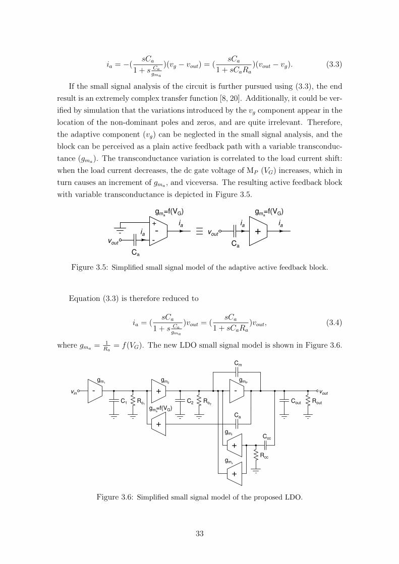
ia = −(sCa
1 + s Ca
gma
)(vg − vout) = (sCa
1 + sCaRa
)(vout − vg). (3.3)
If the small signal analysis of the circuit is further pursued using (3.3), the end
result is an extremely complex transfer function [8, 20]. Additionally, it could be ver-
ified by simulation that the variations introduced by the vg component appear in the
location of the non-dominant poles and zeros, and are quite irrelevant. Therefore,
the adaptive component (vg) can be neglected in the small signal analysis, and the
block can be perceived as a plain active feedback path with a variable transconduc-
tance (gma). The transconductance variation is correlated to the load current shift:
when the load current decreases, the dc gate voltage of MP (VG) increases, which in
turn causes an increment of gma , and viceversa. The resulting active feedback block
with variable transconductance is depicted in Figure 3.5.
gma
-
+
vout
ia
Ca
ia -ia
+
=f(VG)
vout
ia
Ca
gma=f(VG)
Figure 3.5: Simplified small signal model of the adaptive active feedback block.
Equation (3.3) is therefore reduced to
ia = (sCa
1 + s Ca
gma
)vout = (sCa
1 + sCaRa
)vout, (3.4)
where gma = 1Ra
= f(VG). The new LDO small signal model is shown in Figure 3.6.
+
gm2
C2 Ro2
vin vout-
gm1
C1 Ro1
-
gmP
Cout Rout
Ca
Cm
gma
Ccc
Rcc
+
gmf
+
gmx
+
=f(VG)
Figure 3.6: Simplified small signal model of the proposed LDO.
33
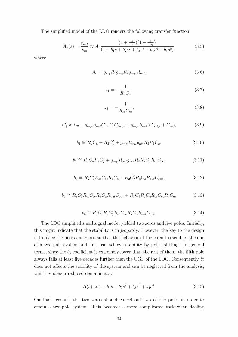
The simplified model of the LDO renders the following transfer function:
Av(s) =voutvin≈ Ao
(1 + s−z1 )(1 + s
−z2 )
(1 + b1s+ b2s2 + b3s3 + b4s4 + b5s5), (3.5)
where
Ao = gm1R1gm2R2gmPRout, (3.6)
z1 = − 1
RaCa, (3.7)
z2 = − 1
RccCcc, (3.8)
C ′2 ≈ C2 + gmPRoutCm ∼= CGSP
+ gmPRout(CGDP
+ Cm), (3.9)
b1 ∼= RaCa +R2C′2 + gmP
Routgm2R2R1Ca, (3.10)
b2 ∼= RaCaR2C′2 + gmP
RoutgmfR2RaCaRccCcc, (3.11)
b3 ∼= R2C′2RccCccRaCa +R2C
′2RaCaRoutCout, (3.12)
b4 ∼= R2C′2RccCccRaCaRoutCout +R1C1R2C
′2RccCccRaCa, (3.13)
b5 ∼= R1C1R2C′2RccCccRaCaRoutCout. (3.14)
The LDO simplified small signal model yielded two zeros and five poles. Initially,
this might indicate that the stability is in jeopardy. However, the key to the design
is to place the poles and zeros so that the behavior of the circuit resembles the one
of a two-pole system and, in turn, achieve stability by pole splitting. In general
terms, since the b5 coefficient is extremely lower than the rest of them, the fifth pole
always falls at least five decades further than the UGF of the LDO. Consequently, it
does not affects the stability of the system and can be neglected from the analysis,
which renders a reduced denominator:
B(s) ≈ 1 + b1s+ b2s2 + b3s
3 + b4s4. (3.15)
On that account, the two zeros should cancel out two of the poles in order to
attain a two-pole system. This becomes a more complicated task when dealing
34
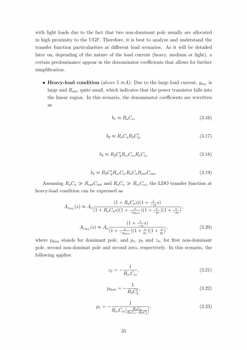
with light loads due to the fact that two non-dominant pole usually are allocated
in high proximity to the UGF. Therefore, it is best to analyze and understand the
transfer function particularities at different load scenarios. As it will be detailed
later on, depending of the nature of the load current (heavy, medium or light), a
certain predominance appear in the denominator coefficients that allows for further
simplification.
• Heavy-load condition (above 5 mA): Due to the large load current, gmPis
large and Rout, quite small, which indicates that the power transistor falls into
the linear region. In this scenario, the denominator coefficients are rewritten
as
b1 ≈ RaCa, (3.16)
b2 ≈ RaCaR2C′2, (3.17)
b3 ≈ R2C′2RccCccRaCa, (3.18)
b4 ≈ R2C′2RccCccRaCaRoutCout. (3.19)
Assuming RaCa RoutCout and RaCa RccCcc, the LDO transfer function at
heavy-load condition can be expressed as
AvHL(s) ≈ Ao
(1 +RaCas)(1 + 1−z2 s)
(1 +RaCas)(1 + s−pdom
)(1 + s−p1 )(1 + s
−p2 ),
AvHL(s) ≈ Ao
(1 + 1−z2 s)
(1 + s−pdom
)(1 + sp1
)(1 + sp2
), (3.20)
where pdom stands for dominant pole, and p1, p2 and z3, for first non-dominant
pole, second non-dominat pole and second zero, respectively. In this scenario, the
following applies:
z2 = − 1
RccCcc, (3.21)
pdom = − 1
R2C ′2, (3.22)
p1 = − 1
RccCcc[RaCa
RaCa−R2C′2], (3.23)
35
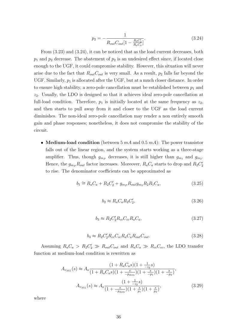
p2 = − 1
RoutCout[1− R2C′2
RaCa]. (3.24)
From (3.23) and (3.24), it can be noticed that as the load current decreases, both
p1 and p2 decrease. The abatement of p2 is an undesired effect since, if located close
enough to the UGF, it could compromise stability. However, this situation will never
arise due to the fact that RoutCout is very small. As a result, p2 falls far beyond the
UGF. Similarly, p1 is allocated after the UGF, but at a much closer distance. In order
to ensure high stability, a zero-pole cancellation must be established between p1 and
z2. Usually, the LDO is designed so that it achieves ideal zero-pole cancellation at
full-load condition. Therefore, p1 is initially located at the same frequency as z2,
and then starts to pull away from it and closer to the UGF as the load current
diminishes. The non-ideal zero-pole cancellation may render a non entirely smooth
gain and phase responses; nonetheless, it does not compromise the stability of the
circuit.
• Medium-load condition (between 5 mA and 0.5 mA): The power transistor
falls out of the linear region, and the system starts working as a three-stage
amplifier. Thus, though gmPdecreases, it is still higher than gm1 and gm2 .
Hence, the gmPRout factor increases. Moreover, RaCa starts to drop and R2C
′2
to rise. The denominator coefficients can be approximated as
b1 ∼= RaCa +R2C′2 + gmP
Routgm2R2R1Ca, (3.25)
b2 ≈ RaCaR2C′2, (3.26)
b3 ≈ R2C′2RccCccRaCa, (3.27)
b4 ≈ R2C′2RccCccRaCaRoutCout. (3.28)
Assuming RaCa > R2C′2 RoutCout and RaCa RccCcc, the LDO transfer
function at medium-load condition is rewritten as
AvML(s) ≈ Ao
(1 +RaCas)(1 + 1−z2 s)
(1 +RaCas)(1 + s−pdom
)(1 + s−p1 )(1 + s
−p2 ),
AvML(s) ≈ Ao
(1 + 1−z2 s)
(1 + s−pdom
)(1 + sp1
)(1 + sp2
), (3.29)
where
36
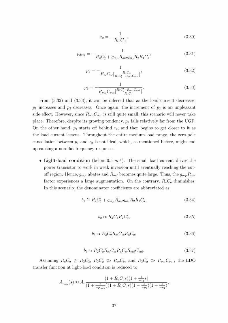
z2 = − 1
RccCcc, (3.30)
pdom = − 1
R2C ′2 + gmPRoutgm2R2R1Ca
, (3.31)
p1 = − 1
RccCcc[RaCa
R2C′2−RoutCout
], (3.32)
p2 = − 1
RoutCout[R2C′
2−RoutCout
RaCa]. (3.33)
From (3.32) and (3.33), it can be inferred that as the load current decreases,
p1 increases and p2 decreases. Once again, the increment of p2 is an unpleasant
side effect. However, since RoutCout is still quite small, this scenario will never take
place. Therefore, despite its growing tendency, p2 falls relatively far from the UGF.
On the other hand, p1 starts off behind z2, and then begins to get closer to it as
the load current lessens. Throughout the entire medium-load range, the zero-pole
cancellation between p1 and z2 is not ideal, which, as mentioned before, might end
up causing a non-flat frequency response.
• Light-load condition (below 0.5 mA): The small load current drives the
power transistor to work in weak inversion until eventually reaching the cut-
off region. Hence, gmPabates and Rout becomes quite large. Thus, the gmP
Rout
factor experiences a large augmentation. On the contrary, RaCa diminishes.
In this scenario, the denominator coefficients are abbreviated as
b1 ∼= R2C′2 + gmP
Routgm2R2R1Ca, (3.34)
b2 ≈ RaCaR2C′2, (3.35)
b3 ≈ R2C′2RccCccRaCa, (3.36)
b4 ≈ R2C′2RccCccRaCaRoutCout. (3.37)
Assuming RaCa ≥ R2C2, R2C′2 RccCcc and R2C
′2 RoutCout, the LDO
transfer function at light-load condition is reduced to
AvLL(s) ≈ Ao
(1 +RaCas)(1 + 1−z2 s)
(1 + s−pdom
)(1 +RaCas)(1 + s−p1 )(1 + s
−p2 ),
37
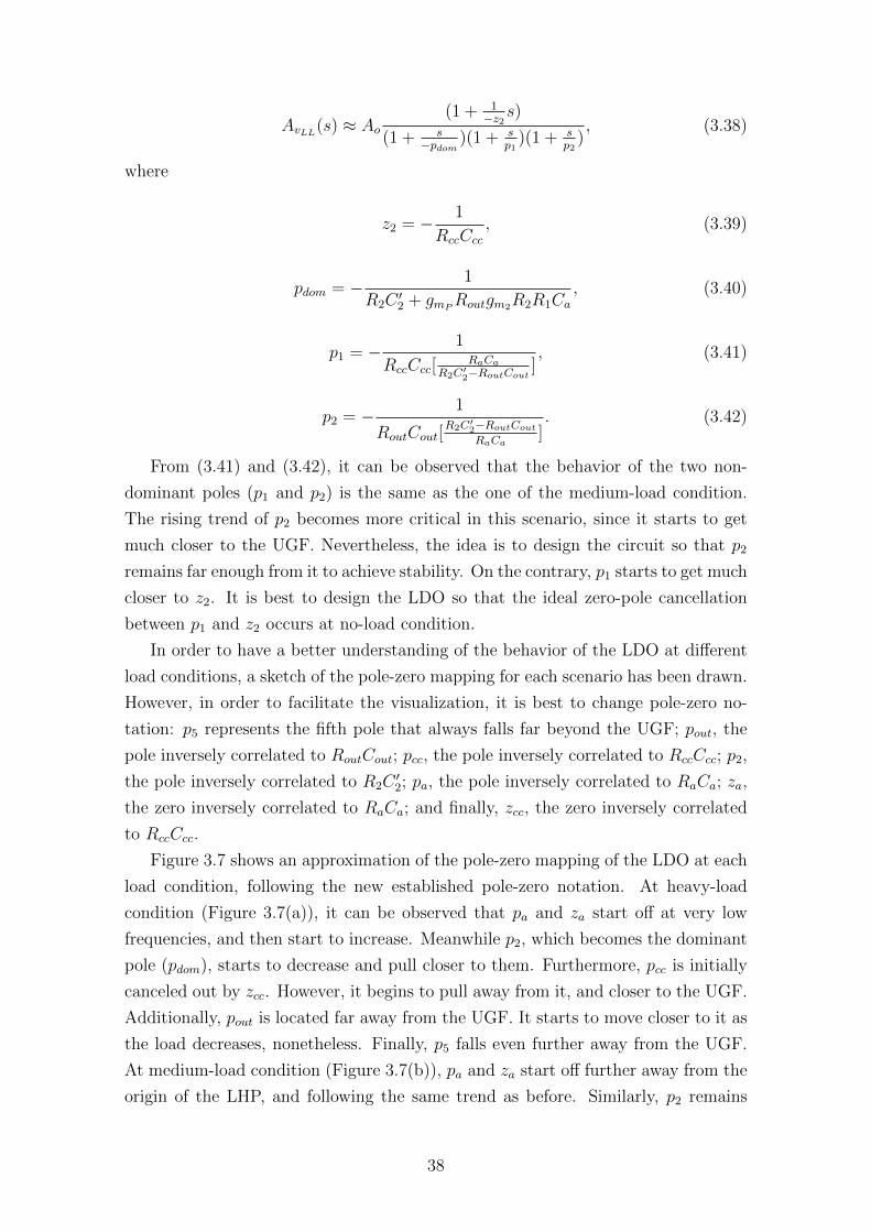
AvLL(s) ≈ Ao
(1 + 1−z2 s)
(1 + s−pdom
)(1 + sp1
)(1 + sp2
), (3.38)
where
z2 = − 1
RccCcc, (3.39)
pdom = − 1
R2C ′2 + gmPRoutgm2R2R1Ca
, (3.40)
p1 = − 1
RccCcc[RaCa
R2C′2−RoutCout
], (3.41)
p2 = − 1
RoutCout[R2C′
2−RoutCout
RaCa]. (3.42)
From (3.41) and (3.42), it can be observed that the behavior of the two non-
dominant poles (p1 and p2) is the same as the one of the medium-load condition.
The rising trend of p2 becomes more critical in this scenario, since it starts to get
much closer to the UGF. Nevertheless, the idea is to design the circuit so that p2
remains far enough from it to achieve stability. On the contrary, p1 starts to get much
closer to z2. It is best to design the LDO so that the ideal zero-pole cancellation
between p1 and z2 occurs at no-load condition.
In order to have a better understanding of the behavior of the LDO at different
load conditions, a sketch of the pole-zero mapping for each scenario has been drawn.
However, in order to facilitate the visualization, it is best to change pole-zero no-
tation: p5 represents the fifth pole that always falls far beyond the UGF; pout, the
pole inversely correlated to RoutCout; pcc, the pole inversely correlated to RccCcc; p2,
the pole inversely correlated to R2C′2; pa, the pole inversely correlated to RaCa; za,
the zero inversely correlated to RaCa; and finally, zcc, the zero inversely correlated
to RccCcc.
Figure 3.7 shows an approximation of the pole-zero mapping of the LDO at each
load condition, following the new established pole-zero notation. At heavy-load
condition (Figure 3.7(a)), it can be observed that pa and za start off at very low
frequencies, and then start to increase. Meanwhile p2, which becomes the dominant
pole (pdom), starts to decrease and pull closer to them. Furthermore, pcc is initially
canceled out by zcc. However, it begins to pull away from it, and closer to the UGF.
Additionally, pout is located far away from the UGF. It starts to move closer to it as
the load decreases, nonetheless. Finally, p5 falls even further away from the UGF.
At medium-load condition (Figure 3.7(b)), pa and za start off further away from the
origin of the LHP, and following the same trend as before. Similarly, p2 remains
38
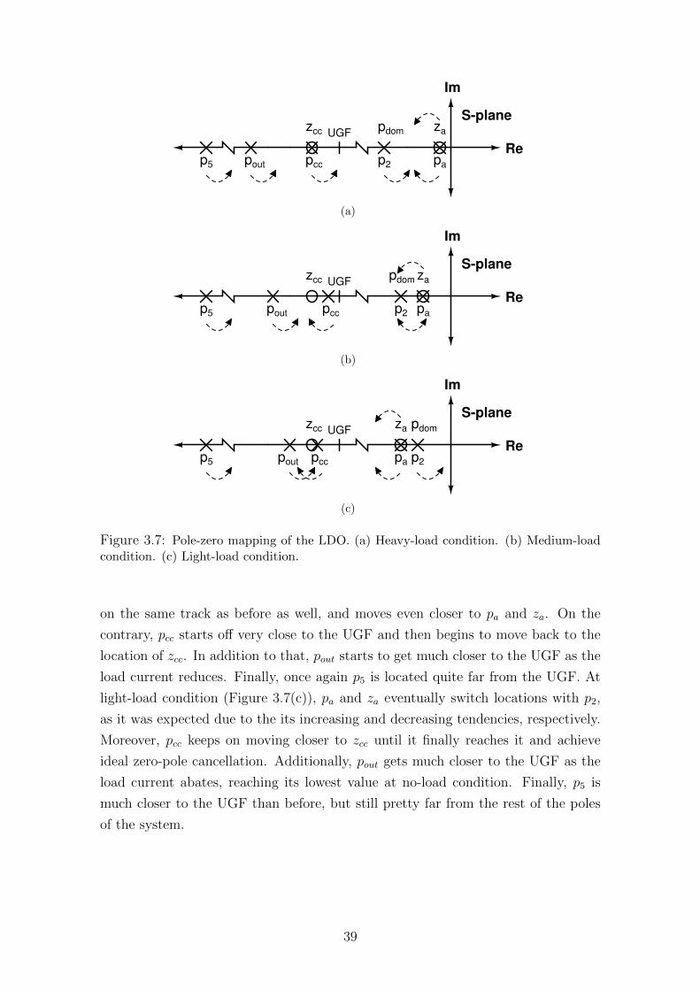
UGF
pa
za
p2pcc
zcc
poutp5
pdom
Im
Re
S-plane
(a)
UGF
pa
za
p2pcc
zcc
poutp5
pdom
Im
Re
S-plane
(b)
UGF
pa
za
p2pcc
zcc
poutp5
pdom
Im
Re
S-plane
(c)
Figure 3.7: Pole-zero mapping of the LDO. (a) Heavy-load condition. (b) Medium-loadcondition. (c) Light-load condition.
on the same track as before as well, and moves even closer to pa and za. On the
contrary, pcc starts off very close to the UGF and then begins to move back to the
location of zcc. In addition to that, pout starts to get much closer to the UGF as the
load current reduces. Finally, once again p5 is located quite far from the UGF. At
light-load condition (Figure 3.7(c)), pa and za eventually switch locations with p2,
as it was expected due to the its increasing and decreasing tendencies, respectively.
Moreover, pcc keeps on moving closer to zcc until it finally reaches it and achieve
ideal zero-pole cancellation. Additionally, pout gets much closer to the UGF as the
load current abates, reaching its lowest value at no-load condition. Finally, p5 is
much closer to the UGF than before, but still pretty far from the rest of the poles
of the system.
39
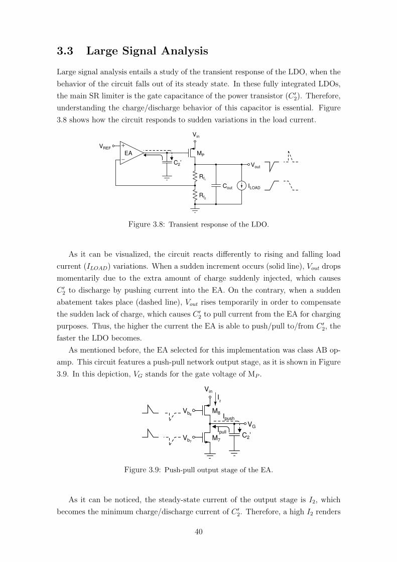
3.3 Large Signal Analysis
Large signal analysis entails a study of the transient response of the LDO, when the
behavior of the circuit falls out of its steady state. In these fully integrated LDOs,
the main SR limiter is the gate capacitance of the power transistor (C ′2). Therefore,
understanding the charge/discharge behavior of this capacitor is essential. Figure
3.8 shows how the circuit responds to sudden variations in the load current.
−
+
C2’
Rf1
Rf2
Cout ILOAD
VREF
Vout
Vin
EA MP
Figure 3.8: Transient response of the LDO.
As it can be visualized, the circuit reacts differently to rising and falling load
current (ILOAD) variations. When a sudden increment occurs (solid line), Vout drops
momentarily due to the extra amount of charge suddenly injected, which causes
C ′2 to discharge by pushing current into the EA. On the contrary, when a sudden
abatement takes place (dashed line), Vout rises temporarily in order to compensate
the sudden lack of charge, which causes C ′2 to pull current from the EA for charging
purposes. Thus, the higher the current the EA is able to push/pull to/from C ′2, the
faster the LDO becomes.
As mentioned before, the EA selected for this implementation was class AB op-
amp. This circuit features a push-pull network output stage, as it is shown in Figure
3.9. In this depiction, VG stands for the gate voltage of MP .
Vin
Vb8
Vb7
M8
M7C2’
VG
Ipush
Ipull
I2
Figure 3.9: Push-pull output stage of the EA.
As it can be noticed, the steady-state current of the output stage is I2, which
becomes the minimum charge/discharge current of C ′2. Therefore, a high I2 renders
40
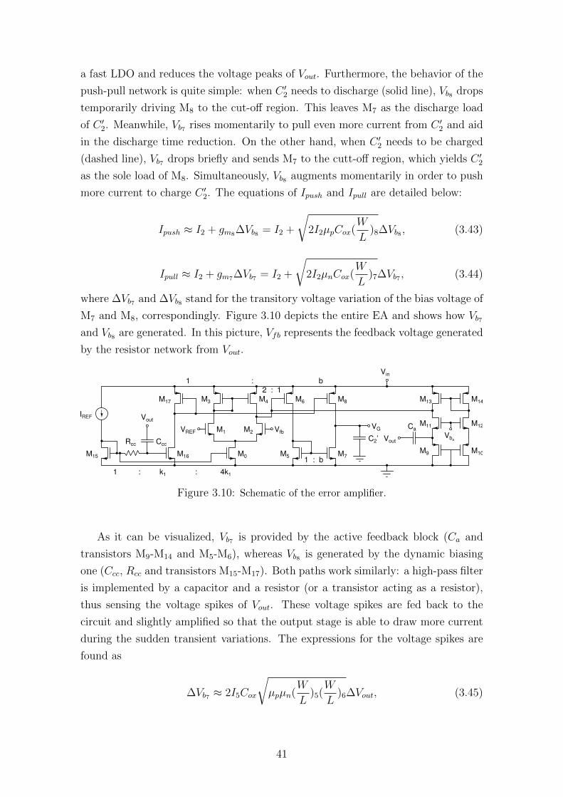
a fast LDO and reduces the voltage peaks of Vout. Furthermore, the behavior of the
push-pull network is quite simple: when C ′2 needs to discharge (solid line), Vb8 drops
temporarily driving M8 to the cut-off region. This leaves M7 as the discharge load
of C ′2. Meanwhile, Vb7 rises momentarily to pull even more current from C ′2 and aid
in the discharge time reduction. On the other hand, when C ′2 needs to be charged
(dashed line), Vb7 drops briefly and sends M7 to the cutt-off region, which yields C ′2
as the sole load of M8. Simultaneously, Vb8 augments momentarily in order to push
more current to charge C ′2. The equations of Ipush and Ipull are detailed below:
Ipush ≈ I2 + gm8∆Vb8 = I2 +
√2I2µpCox(
W
L)8∆Vb8 , (3.43)
Ipull ≈ I2 + gm7∆Vb7 = I2 +
√2I2µnCox(
W
L)7∆Vb7 , (3.44)
where ∆Vb7 and ∆Vb8 stand for the transitory voltage variation of the bias voltage of
M7 and M8, correspondingly. Figure 3.10 depicts the entire EA and shows how Vb7
and Vb8 are generated. In this picture, Vfb represents the feedback voltage generated
by the resistor network from Vout.
VREF
Vout
M0
M1 M2
M3 M4 M6
M5 M7
M8
C2’
VG CaM11 M12
Vba
Vfb
CccRcc
Vout
M16
M14M13M17
M15
IREF
Vin
M9 M10
1 : k1 : 4k1
1 : b
1 : b
2 : 1
Figure 3.10: Schematic of the error amplifier.
As it can be visualized, Vb7 is provided by the active feedback block (Ca and
transistors M9-M14 and M5-M6), whereas Vb8 is generated by the dynamic biasing
one (Ccc, Rcc and transistors M15-M17). Both paths work similarly: a high-pass filter
is implemented by a capacitor and a resistor (or a transistor acting as a resistor),
thus sensing the voltage spikes of Vout. These voltage spikes are fed back to the
circuit and slightly amplified so that the output stage is able to draw more current
during the sudden transient variations. The expressions for the voltage spikes are
found as
∆Vb7 ≈ 2I5Cox
√µpµn(
W
L)5(W
L)6∆Vout, (3.45)
41
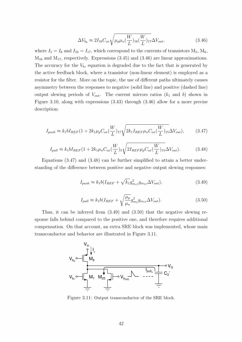
∆Vb8 ≈ 2I16Cox
√µpµn(
W
L)16(
W
L)17∆Vout, (3.46)
where I5 = I6 and I16 = I17, which correspond to the currents of transistors M5, M6,
M16 and M17, respectively. Expressions (3.45) and (3.46) are linear approximations.
The accuracy for the Vb7 equation is degraded due to the fact that is generated by
the active feedback block, where a transistor (non-linear element) is employed as a
resistor for the filter. More on the topic, the use of different paths ultimately causes
asymmetry between the responses to negative (solid line) and positive (dashed line)
output slewing periods of Vout. The current mirrors ratios (k1 and b) shown in
Figure 3.10, along with expressions (3.43) through (3.46) allow for a more precise
description:
Ipush ≈ k1bIREF (1 + 2k1µpCox(W
L)17
√2k1IREFµnCox(
W
L)15∆Vout), (3.47)
Ipull ≈ k1bIREF (1 + 2k1µnCox(W
L)5
√2IREFµpCox(
W
L)15∆Vout). (3.48)
Equations (3.47) and (3.48) can be further simplified to attain a better under-
standing of the difference between positive and negative output slewing responses:
Ipush ≈ k1b(IREF +√k1g
2m17
gm15∆Vout), (3.49)
Ipull ≈ k1b(IREF +
√µpµng2m5
gm15∆Vout). (3.50)
Thus, it can be inferred from (3.49) and (3.50) that the negative slewing re-
sponse falls behind compared to the positive one, and therefore requires additional
compensation. On that account, an extra SRE block was implemented, whose main
transconductor and behavior are illustrated in Figure 3.11.
Vin
Vb8
Vb7
M8
M7
C2’
VGIpulle
I2
M25 VbSRE
Figure 3.11: Output transconductor of the SRE block.
42
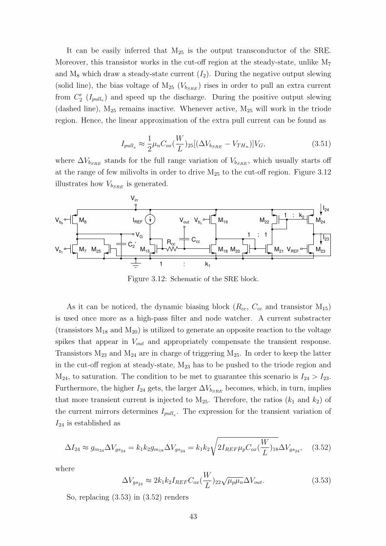
It can be easily inferred that M25 is the output transconductor of the SRE.
Moreover, this transistor works in the cut-off region at the steady-state, unlike M7
and M8 which draw a steady-state current (I2). During the negative output slewing
(solid line), the bias voltage of M25 (VbSRE) rises in order to pull an extra current
from C ′2 (Ipulle) and speed up the discharge. During the positive output slewing
(dashed line), M25 remains inactive. Whenever active, M25 will work in the triode
region. Hence, the linear approximation of the extra pull current can be found as
Ipulle ≈1
2µnCox(
W
L)25[(∆VbSRE
− VTHn)]VG, (3.51)
where ∆VbSREstands for the full range variation of VbSRE
, which usually starts off
at the range of few milivolts in order to drive M25 to the cut-off region. Figure 3.12
illustrates how VbSREis generated.
Vout Vbs
CccRcc
VG
M15 M18
M19
M7
M8
M20 M21 VREF
IREF M22
M23
M24
M25
Vin
Vb8
Vb7
1 : k2
1 : 1
C2’
I24
I23
1 : k1
Figure 3.12: Schematic of the SRE block.
As it can be noticed, the dynamic biasing block (Rcc, Ccc and transistor M15)
is used once more as a high-pass filter and node watcher. A current substracter
(transistors M18 and M20) is utilized to generate an opposite reaction to the voltage
spikes that appear in Vout and appropriately compensate the transient response.
Transistors M23 and M24 are in charge of triggering M25. In order to keep the latter
in the cut-off region at steady-state, M23 has to be pushed to the triode region and
M24, to saturation. The condition to be met to guarantee this scenario is I24 > I23.
Furthermore, the higher I24 gets, the larger ∆VbSREbecomes, which, in turn, implies
that more transient current is injected to M25. Therefore, the ratios (k1 and k2) of
the current mirrors determines Ipulle . The expression for the transient variation of
I24 is established as
∆I24 ≈ gm24∆Vgs24 = k1k2gm18∆Vgs24 = k1k2
√2IREFµpCox(
W
L)18∆Vgs24 , (3.52)
where
∆Vgs24 ≈ 2k1k2IREFCox(W
L)22√µpµn∆Vout. (3.53)
So, replacing (3.53) in (3.52) renders
43
∆I24 ≈ 2k21k22IREFµpCox(
W
L)22
√2IREFµnCOX(
W
L)18∆Vout, (3.54)
which can also be rewritten as
∆I24 ≈ k1k2g2m22
gm18∆Vout. (3.55)
Ultimately, the actual variation of VbSREcan be found as
∆VbSRE≈ ∆I24RON23 ≈ k1k2g
2m22
gm18RON23∆Vout, (3.56)
where
∆RON23 ≈2
µnCoxVOV 23(WL
)23=
2
µnCox(VREF − VTHn)(WL
)23. (3.57)
In this case, VOV 23 represents the overdrive voltage of M23. From (3.56) it can
be noticed that gm18 and specially gm22 basically determine ∆VbSRE, and therefore
should be as large as possible without compromising the power consumption.
Besides the amount of transient current generated, the speed of the circuit is
critical as well. The response time of the SRE block depends essentially on how fast
the circuit is able to activate M25. Thus, the expression for the response time is
found as
trespSRE=
∆VON25Cp25∆I24
≈ (VTHn − VOV 23)Cp25k1k2g2m22
gm18∆Vout, (3.58)
where Cp25 , the parasitic capacitance at the gate of M25. It can be deduced from (3.58
that the response time increases with Cp25 , which is not desirable. Consequently,
(WL
)25 should be kept low in order to augment the speed of the SRE block. Fur-
thermore, enlarging gm22 and gm18 - specially the former due to its inverse quadratic
correlation - while maintaining the power consumption at a minimum seems to be
the best practice to reduce the response time.
Finally, the size of the voltage peaks of the output voltage can be estimated as
well. Recalling Figure 3.8, the negative output slewing (solid line) constitutes an
undershoot, and the positive one (dashed line), an overshoot. The appearance of
these voltage spikes is caused by the sudden charge shift that Cout experiences. When
ILOAD suddenly rises, MP is not able to provide the current immediately. Therefore,
Cout starts to discharge in order to deliver the current to the load, which causes Vout
to drop. On the other hand, when ILOAD falls abruptly, MP is incapable of turning
off its current instantaneously. This leaves Cout overcharged, which translates to an
increment of Vout. Thus, The push-pull network and the SRE block are put in place
to compensate for the lack/excess of charge through VG. At any given time, the
44
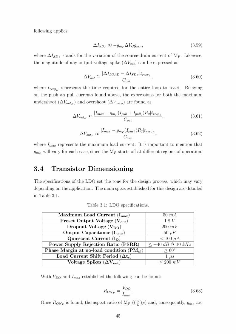
following applies:
∆ISDP≈ −gmP
∆VGgmP, (3.59)
where ∆ISDPstands for the variation of the source-drain current of MP . Likewise,
the magnitude of any output voltage spike (∆Vout) can be expressed as
∆Vout ∼=|∆ILOAD −∆ISDP
|trespLCout
, (3.60)
where trespL represents the time required for the entire loop to react. Relaying
on the push an pull currents found above, the expressions for both the maximum
undershoot (∆VoutN ) and overshoot (∆VoutP ) are found as
∆VoutN ≈|Imax − gmP
(Ipull + Ipulle)R2|trespLCout
, (3.61)
∆VoutP ≈|Imax − gmP
(Ipush)R2|trespLCout
, (3.62)
where Imax represents the maximum load current. It is important to mention that
gmPwill vary for each case, since the MP starts off at different regions of operation.
3.4 Transistor Dimensioning
The specifications of the LDO set the tone for the design process, which may vary
depending on the application. The main specs established for this design are detailed
in Table 3.1.
Table 3.1: LDO specifications.
Maximum Load Current (Imax) 50 mAPreset Output Voltage (Vout) 1.8 V
Dropout Voltage (VDO) 200 mVOutput Capacitance (Cout) 50 pF
Quiescent Current (IQ) < 100 µAPower Supply Rejection Ratio (PSRR) ≤ −40 dB @ 10 kHz
Phase Margin at no-load condition (PMnl) ≥ 60
Load Current Shift Period (∆ts) 1 µsVoltage Spikes (∆Vout) ≤ 200 mV
With VDO and Imax established the following can be found:
RONP=VDOImax
. (3.63)
Once RONPis found, the aspect ratio of MP ((W
L)P ) and, consequently, gmP
are
45
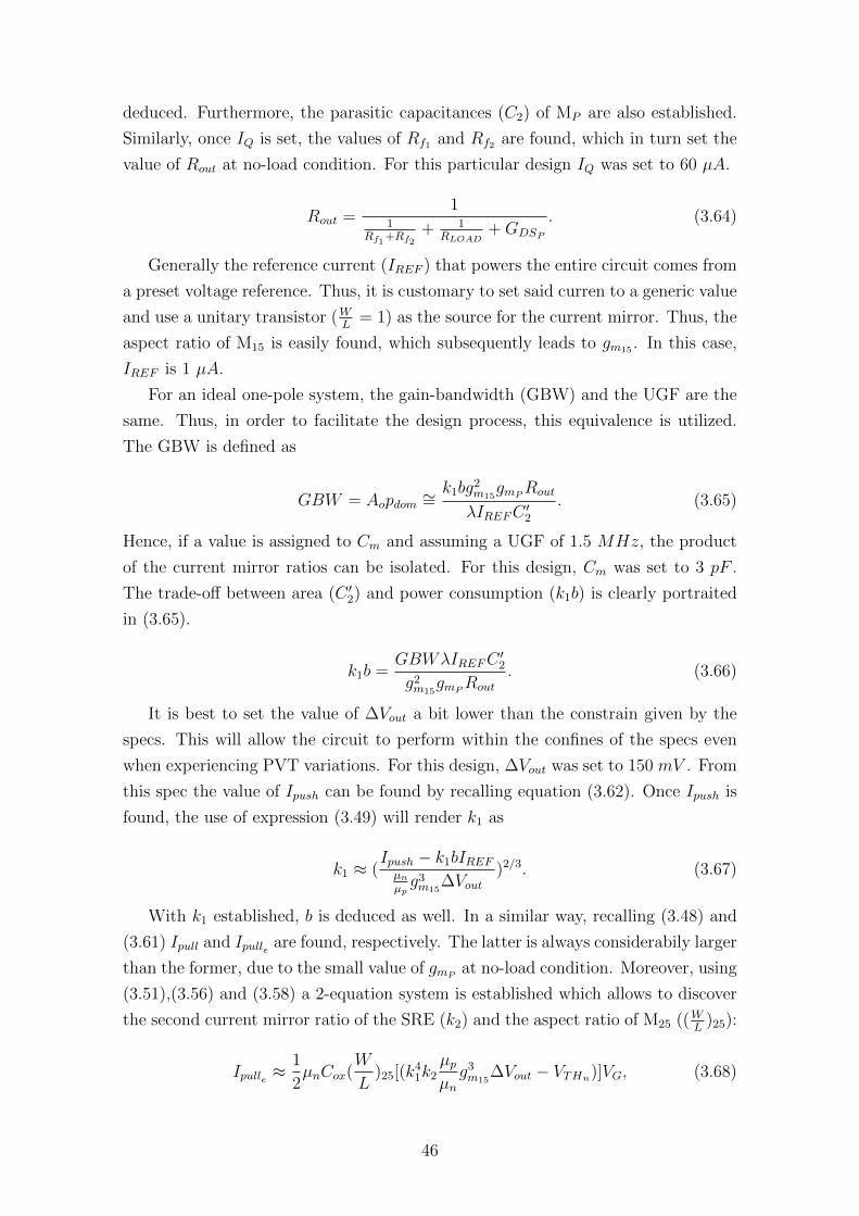
deduced. Furthermore, the parasitic capacitances (C2) of MP are also established.
Similarly, once IQ is set, the values of Rf1 and Rf2 are found, which in turn set the
value of Rout at no-load condition. For this particular design IQ was set to 60 µA.
Rout =1
1Rf1
+Rf2+ 1
RLOAD+GDSP
. (3.64)
Generally the reference current (IREF ) that powers the entire circuit comes from
a preset voltage reference. Thus, it is customary to set said curren to a generic value
and use a unitary transistor (WL
= 1) as the source for the current mirror. Thus, the
aspect ratio of M15 is easily found, which subsequently leads to gm15 . In this case,
IREF is 1 µA.
For an ideal one-pole system, the gain-bandwidth (GBW) and the UGF are the
same. Thus, in order to facilitate the design process, this equivalence is utilized.
The GBW is defined as
GBW = Aopdom ∼=k1bg
2m15
gmPRout
λIREFC ′2. (3.65)
Hence, if a value is assigned to Cm and assuming a UGF of 1.5 MHz, the product
of the current mirror ratios can be isolated. For this design, Cm was set to 3 pF .
The trade-off between area (C ′2) and power consumption (k1b) is clearly portraited
in (3.65).
k1b =GBWλIREFC
′2
g2m15gmP
Rout
. (3.66)
It is best to set the value of ∆Vout a bit lower than the constrain given by the
specs. This will allow the circuit to perform within the confines of the specs even
when experiencing PVT variations. For this design, ∆Vout was set to 150 mV . From
this spec the value of Ipush can be found by recalling equation (3.62). Once Ipush is
found, the use of expression (3.49) will render k1 as
k1 ≈ (Ipush − k1bIREFµnµpg3m15
∆Vout)2/3. (3.67)
With k1 established, b is deduced as well. In a similar way, recalling (3.48) and
(3.61) Ipull and Ipulle are found, respectively. The latter is always considerabily larger
than the former, due to the small value of gmPat no-load condition. Moreover, using
(3.51),(3.56) and (3.58) a 2-equation system is established which allows to discover
the second current mirror ratio of the SRE (k2) and the aspect ratio of M25 ((WL
)25):
Ipulle ≈1
2µnCox(
W
L)25[(k
41k2
µpµng3m15
∆Vout − VTHn)]VG, (3.68)
46
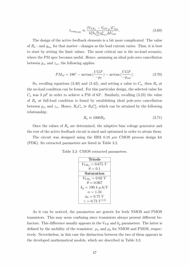
trespSRE≈ (VTHn − VOV 23)Cp25
k41k2µpµng3m15
∆Vout. (3.69)
The design of the active feedback elements is a bit more complicated. The value
of Ra - and gma for that matter - changes as the load current varies. Thus, it is best
to start by setting the limit values. The most critical one is the no-load scenario,
where the PM spec becomes useful. Hence, assuming an ideal pole-zero cancellation
between pcc and zcc, the following applies:
PMnl = 180 − arctan (UGF
−p2)− arctan (
UGF
−pout). (3.70)
So, recalling equations (3.40) and (3.42), and setting a value to Ca, then Ra at
the no-load condition can be found. For this particular design, the selected value for
Ca was 3 pF in order to achieve a PM of 63. Similarly, recalling (3.23) the value
of Ra at full-load condition is found by establishing ideal pole-zero cancellation
between pcc and zcc. Hence, RaCa R2C′2, which can be attained by the following
relationship:
Ra ≈ 1000R2. (3.71)
Once the values of Ra are determined, the adaptive bias voltage generator and
the rest of the active feedback circuit is sized and optimized in order to attain them.
The circuit was designed using the IBM 0.18 µm CMOS process design kit
(PDK). Its extracted parameters are listed in Table 3.2.
Table 3.2: CMOS extracted parameters.
TriodeVTH0 = 0.675 V
θ = 0.1SaturationVTH0 = 0.62 Vθ = 0.067
kp = 190.4 µA/Vα = 1.34
φ0 = 0.75 Vγ = 0.73 V 1/2
As it can be noticed, the parameters are generic for both NMOS and PMOS
transistors. This may seem confusing since transistors always present different be-
haviors. This difference usually appears in the VTH and kp parameters. The latter is
defined by the mobility of the transistor: µn and µp for NMOS and PMOS, respec-
tively. Nevertheless, in this case the distinction between the two of them appears in
the developed mathematical models, which are described in Table 3.3.
47
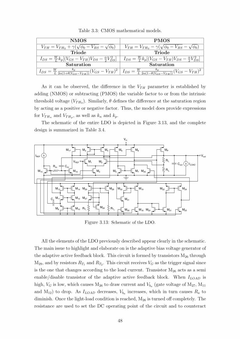
Table 3.3: CMOS mathematical models.
NMOS PMOSVTH = VTH0 + γ(
√φ0 − VBS −
√φ0) VTH = VTH0 − γ(
√φ0 − VBS −
√φ0)
Triode TriodeIDS = W
Lkp[(VGS − VTH)VDS − α
2V 2DS] IDS = W
Lkp[(VGS − VTH)VDS − α
2V 2DS]
Saturation Saturation
IDS = WL
kp2α(1+θ(VGS−VTH))
(VGS − VTH)2 IDS = WL
kp2α(1−θ(VGS−VTH))
(VGS − VTH)2
As it can be observed, the difference in the VTH parameter is established by
adding (NMOS) or subtracting (PMOS) the variable factor to or from the intrinsic
threshold voltage (VTH0). Similarly, θ defines the difference at the saturation region
by acting as a positive or negative factor. Thus, the model does provide expressions
for VTHn and VTHp , as well as kn and kp.
The schematic of the entire LDO is depicted in Figure 3.13, and the complete
design is summarized in Table 3.4.
VREF
M0
M1 M2
M3 M4 M6
M5 M7
M8
CaM11 M12
CccRcc
M16
M14M13
M17
M15
IREF
Vin
M9 M10
MP
Rf1
Rf2
Cout ILOAD
M26RT1
M27
M29 M28
RT2
M25
M18
M19
M20M30
M31
M32
M21
M22 M24
M23
Vout
Figure 3.13: Schematic of the LDO.
All the elements of the LDO previously described appear clearly in the schematic.
The main issue to highlight and elaborate on is the adaptive bias voltage generator of
the adaptive active feedback block. This circuit is formed by transistors M26 through
M29, and by resistors RT1 and RT2 . This circuit receives VG as the trigger signal since
is the one that changes according to the load current. Transistor M26 acts as a semi
enable/disable transistor of the adaptive active feedback block. When ILOAD is
high, VG is low, which causes M26 to draw current and Vba (gate voltage of M27, M11
and M12) to drop. As ILOAD decreases, Vba increases, which in turn causes Ra to
diminish. Once the light-load condition is reached, M26 is turned off completely. The
resistance are used to set the DC operating point of the circuit and to counteract
48
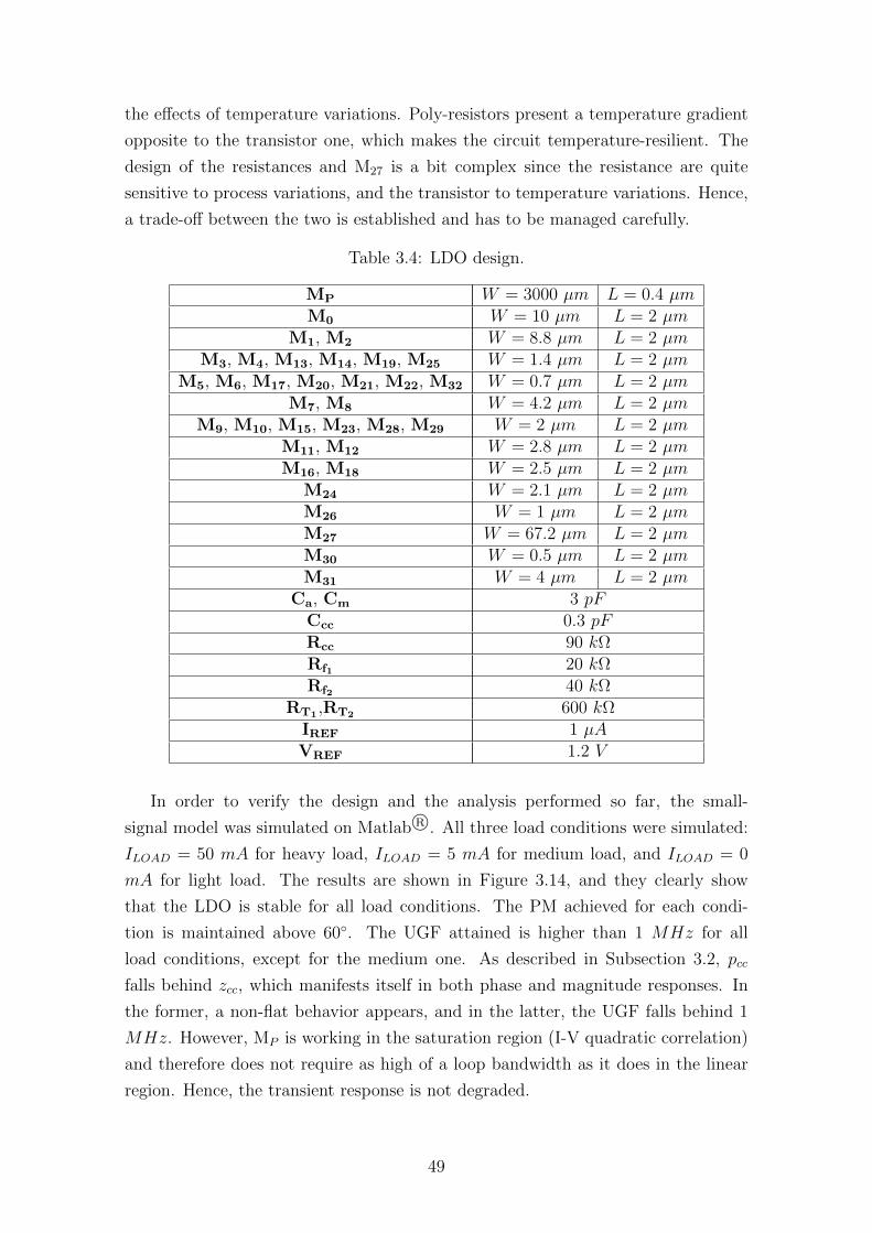
the effects of temperature variations. Poly-resistors present a temperature gradient
opposite to the transistor one, which makes the circuit temperature-resilient. The
design of the resistances and M27 is a bit complex since the resistance are quite
sensitive to process variations, and the transistor to temperature variations. Hence,
a trade-off between the two is established and has to be managed carefully.
Table 3.4: LDO design.
MP W = 3000 µm L = 0.4 µmM0 W = 10 µm L = 2 µm
M1, M2 W = 8.8 µm L = 2 µmM3, M4, M13, M14, M19, M25 W = 1.4 µm L = 2 µm
M5, M6, M17, M20, M21, M22, M32 W = 0.7 µm L = 2 µmM7, M8 W = 4.2 µm L = 2 µm
M9, M10, M15, M23, M28, M29 W = 2 µm L = 2 µmM11, M12 W = 2.8 µm L = 2 µmM16, M18 W = 2.5 µm L = 2 µm
M24 W = 2.1 µm L = 2 µmM26 W = 1 µm L = 2 µmM27 W = 67.2 µm L = 2 µmM30 W = 0.5 µm L = 2 µmM31 W = 4 µm L = 2 µm
Ca, Cm 3 pFCcc 0.3 pFRcc 90 kΩRf1 20 kΩRf2 40 kΩ
RT1 ,RT2 600 kΩIREF 1 µAVREF 1.2 V
In order to verify the design and the analysis performed so far, the small-
signal model was simulated on Matlab R©. All three load conditions were simulated:
ILOAD = 50 mA for heavy load, ILOAD = 5 mA for medium load, and ILOAD = 0
mA for light load. The results are shown in Figure 3.14, and they clearly show
that the LDO is stable for all load conditions. The PM achieved for each condi-
tion is maintained above 60. The UGF attained is higher than 1 MHz for all
load conditions, except for the medium one. As described in Subsection 3.2, pcc
falls behind zcc, which manifests itself in both phase and magnitude responses. In
the former, a non-flat behavior appears, and in the latter, the UGF falls behind 1
MHz. However, MP is working in the saturation region (I-V quadratic correlation)
and therefore does not require as high of a loop bandwidth as it does in the linear
region. Hence, the transient response is not degraded.
49
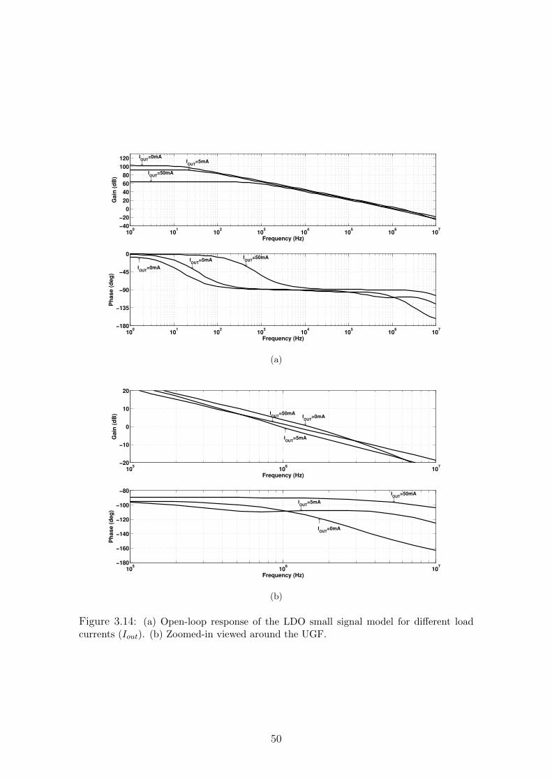
100
101
102
103
104
105
106
107
−40
−20
0
20
40
60
80
100
120
Gain
(d
B)
Frequency (Hz)
IOUT
=0mA
↓ IOUT
=5mA
↓IOUT
=50mA
↓
100
101
102
103
104
105
106
107
−180
−135
−90
−45
0
Ph
ase (
deg
)
Frequency (Hz)
IOUT
=50mA
↓IOUT
=5mA
↓
↑
IOUT
=0mA
(a)
105
106
107
−20
−10
0
10
20
Gain
(d
B)
Frequency (Hz)
↑
IOUT
=5mA
IOUT
=50mA
↓IOUT
=0mA
↓
105
106
107
−180
−160
−140
−120
−100
−80
Ph
ase (
deg
)
Frequency (Hz)
IOUT
=50mA
↓IOUT
=5mA
↓
↑
IOUT
=0mA
(b)
Figure 3.14: (a) Open-loop response of the LDO small signal model for different loadcurrents (Iout). (b) Zoomed-in viewed around the UGF.
50
Chapter 4
Layout Design
LDO layout design always present some challenges compared to any other regular cir-
cuit. The reason for this is the excessive amount of current that has to be generated
and transported through the die. Special considerations must be taken in order to
avoid undesired effects, such as electromigration (EM) [23]. Furthermore, the power
transistor (MP ) and the compensation capacitors (Ca, Cm and Ccc) tend to occupy
a large amount of area. Therefore, proper placing and design of these elements is
key to reduce the size of the integrated circuit. Additionally, mismatch effects have
to be taken under consideration, specially for the resistive feedback network (Rf1
and Rf2), in order to minimize the random offset of the preset output voltage (Vout).
Hence, some particular layout techniques were used on the key elements of the LDO
in order to render an integrated circuit able to withstand mismatch effects. On that
account, this chapter will illustrate the layout of the aforementioned key elements
and will give a description of the layout techniques used to address these issues.
Ultimately, the complete layout design is depicted.
4.1 Power Transistor
One of the first elements to analyze while realizing the layout design is the power
transistor. Due to its large width (W ), the use of fingers comes in handy to make a
much more efficient use of the die area. A side effect of this technique is the reduction
of the parasitic capacitances associated with said transistor (C2). Furthermore, the
distribution of the extremely high current through several instances reduces the
size of the metal paths that connect MP to the input supply voltage (Vin). In
this particular design, the power transistor was stripped down to 300 instances of
W = 10 µm. Ultimately, they were organized to conform 5 instances, each one with
60 fingers of W = 10 µm, as it can be observed in Figure 4.1. As it can be observed,
transistor chaining is employed to reduced the amount of active area. Thus, source
(S) and drain (D) terminals are being shared all throughout each 60 fingers instance.
51
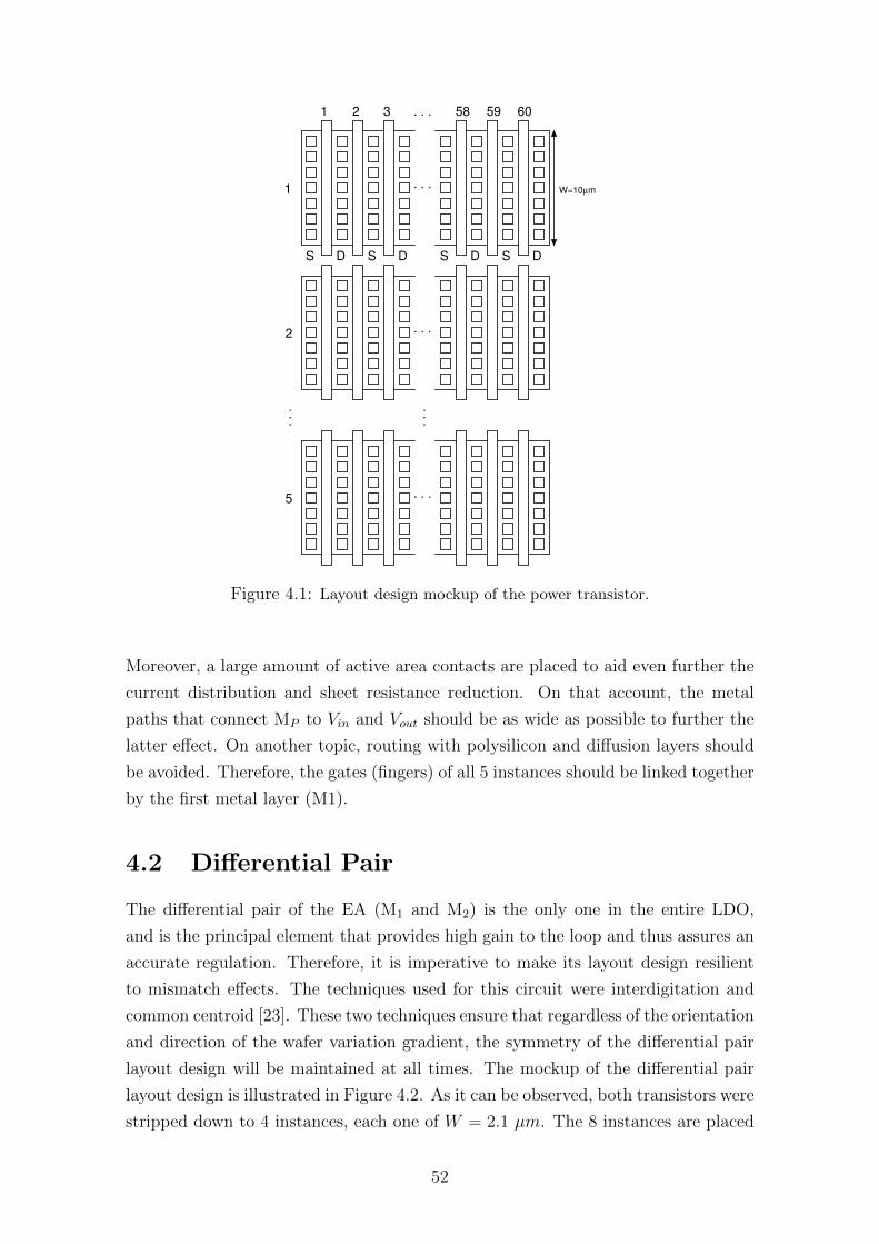
. . .1 2 3 605958
W=10µm. . .
. . .
. . .
. .
.
. .
.
1
2
5
S D S D S D S D
Figure 4.1: Layout design mockup of the power transistor.
Moreover, a large amount of active area contacts are placed to aid even further the
current distribution and sheet resistance reduction. On that account, the metal
paths that connect MP to Vin and Vout should be as wide as possible to further the
latter effect. On another topic, routing with polysilicon and diffusion layers should
be avoided. Therefore, the gates (fingers) of all 5 instances should be linked together
by the first metal layer (M1).
4.2 Differential Pair
The differential pair of the EA (M1 and M2) is the only one in the entire LDO,
and is the principal element that provides high gain to the loop and thus assures an
accurate regulation. Therefore, it is imperative to make its layout design resilient
to mismatch effects. The techniques used for this circuit were interdigitation and
common centroid [23]. These two techniques ensure that regardless of the orientation
and direction of the wafer variation gradient, the symmetry of the differential pair
layout design will be maintained at all times. The mockup of the differential pair
layout design is illustrated in Figure 4.2. As it can be observed, both transistors were
stripped down to 4 instances, each one of W = 2.1 µm. The 8 instances are placed
52
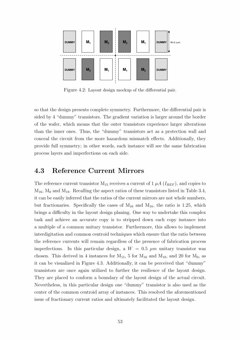
M1M1
M1 M1 W=2.1µmM2M2
M2 M2
DUMMY
DUMMY
DUMMY
DUMMY
Figure 4.2: Layout design mockup of the differential pair.
so that the design presents complete symmetry. Furthermore, the differential pair is
sided by 4 “dummy” transistors. The gradient variation is larger around the border
of the wafer, which means that the outer transistors experience larger alterations
than the inner ones. Thus, the “dummy” transistors act as a protection wall and
conceal the circuit from the more hazardous mismatch effects. Additionally, they
provide full symmetry; in other words, each instance will see the same fabrication
process layers and imperfections on each side.
4.3 Reference Current Mirrors
The reference current transistor M15 receives a current of 1 µA (IREF ), and copies to
M16, M0 and M18. Recalling the aspect ratios of these transistors listed in Table 3.4,
it can be easily inferred that the ratios of the current mirrors are not whole numbers,
but fractionaries. Specifically the cases of M16 and M18, the ratio is 1.25, which
brings a difficulty in the layout design planing. One way to undertake this complex
task and achieve an accurate copy is to stripped down each copy instance into
a multiple of a common unitary transistor. Furthermore, this allows to implement
interdigitation and common centroid techniques which ensure that the ratio between
the reference currents will remain regardless of the presence of fabrication process
imperfections. In this particular design, a W = 0.5 µm unitary transistor was
chosen. This derived in 4 instances for M15, 5 for M16 and M18, and 20 for M0, as
it can be visualized in Figure 4.3. Additionally, it can be perceived that “dummy”
transistors are once again utilized to further the resilience of the layout design.
They are placed to conform a boundary of the layout design of the actual circuit.
Nevertheless, in this particular design one “dummy” transistor is also used as the
center of the common centroid array of instances. This resolved the aforementioned
issue of fractionary current ratios and ultimately facilitated the layout design.
53
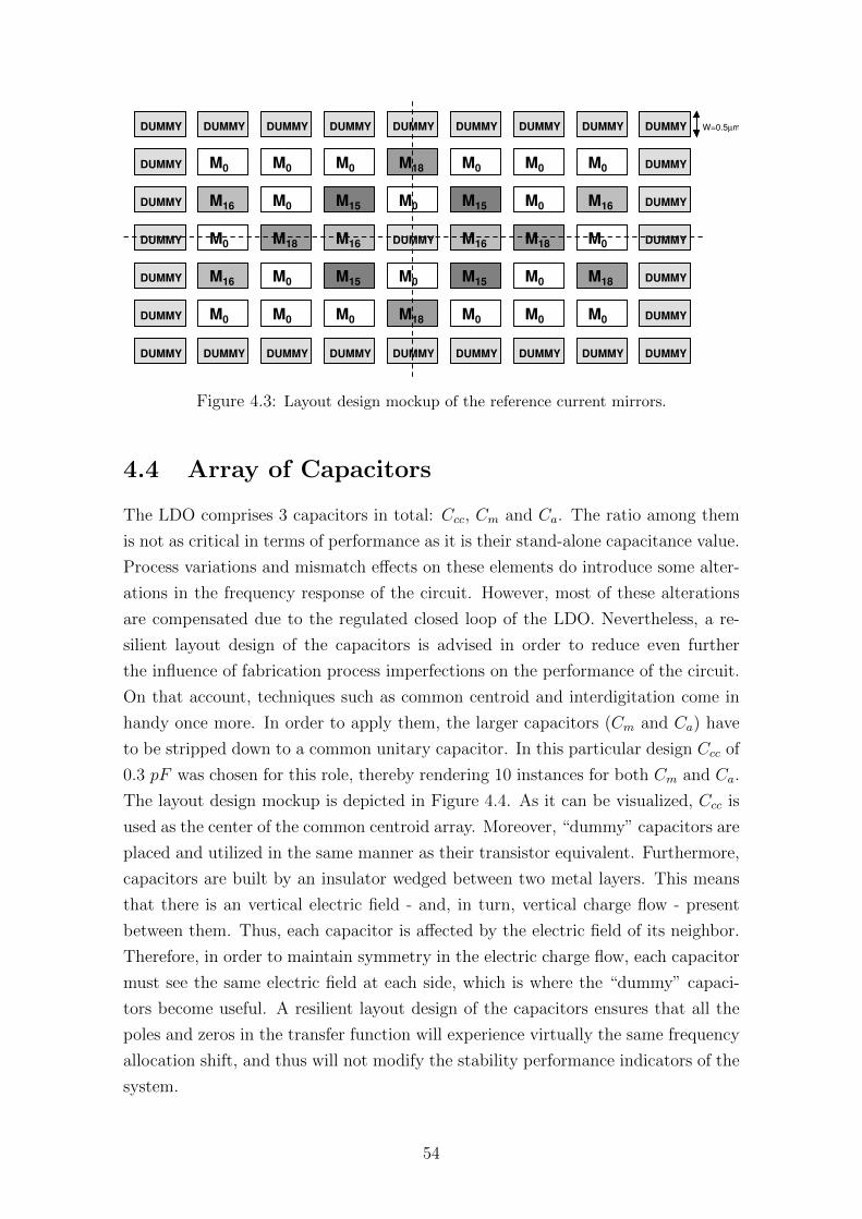
M0
M0M0
M0 M0
M0
M0 M0
M0M0M0M0M0M0
M0 M0 M0 M0 M0 M0
W=0.5µmDUMMY DUMMY DUMMY DUMMY DUMMY DUMMY DUMMY DUMMY DUMMY
DUMMY
DUMMY
DUMMY
DUMMY
DUMMY
DUMMYDUMMYDUMMYDUMMYDUMMYDUMMYDUMMYDUMMYDUMMY
DUMMY
DUMMY
DUMMY
DUMMY
DUMMY
DUMMY
M15 M15
M15M15
M18
M18
M18 M18
M18
M16M16
M16
M16 M16
Figure 4.3: Layout design mockup of the reference current mirrors.
4.4 Array of Capacitors
The LDO comprises 3 capacitors in total: Ccc, Cm and Ca. The ratio among them
is not as critical in terms of performance as it is their stand-alone capacitance value.
Process variations and mismatch effects on these elements do introduce some alter-
ations in the frequency response of the circuit. However, most of these alterations
are compensated due to the regulated closed loop of the LDO. Nevertheless, a re-
silient layout design of the capacitors is advised in order to reduce even further
the influence of fabrication process imperfections on the performance of the circuit.
On that account, techniques such as common centroid and interdigitation come in
handy once more. In order to apply them, the larger capacitors (Cm and Ca) have
to be stripped down to a common unitary capacitor. In this particular design Ccc of
0.3 pF was chosen for this role, thereby rendering 10 instances for both Cm and Ca.
The layout design mockup is depicted in Figure 4.4. As it can be visualized, Ccc is
used as the center of the common centroid array. Moreover, “dummy” capacitors are
placed and utilized in the same manner as their transistor equivalent. Furthermore,
capacitors are built by an insulator wedged between two metal layers. This means
that there is an vertical electric field - and, in turn, vertical charge flow - present
between them. Thus, each capacitor is affected by the electric field of its neighbor.
Therefore, in order to maintain symmetry in the electric charge flow, each capacitor
must see the same electric field at each side, which is where the “dummy” capaci-
tors become useful. A resilient layout design of the capacitors ensures that all the
poles and zeros in the transfer function will experience virtually the same frequency
allocation shift, and thus will not modify the stability performance indicators of the
system.
54
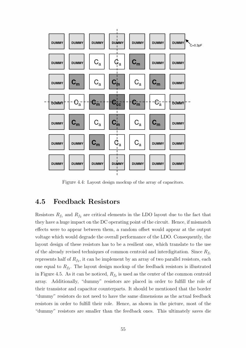
Ca
Ca Ca
Ca
Ca Ca
Ca
Ca Ca
Ca
C=0.3pFDUMMY DUMMY DUMMY DUMMY DUMMY DUMMY DUMMY
DUMMY
DUMMY
DUMMY
DUMMY
DUMMY
DUMMYDUMMYDUMMYDUMMYDUMMYDUMMYDUMMY
DUMMY
DUMMY
DUMMY
DUMMY
DUMMY
DUMMY
DUMMY
DUMMY
CccCm
Cm
Cm
Cm
Cm
Cm
Cm
Cm
CmCm
DUMMY
Figure 4.4: Layout design mockup of the array of capacitors.
4.5 Feedback Resistors
Resistors Rf1 and Rf2 are critical elements in the LDO layout due to the fact that
they have a huge impact on the DC operating point of the circuit. Hence, if mismatch
effects were to appear between them, a random offset would appear at the output
voltage which would degrade the overall performance of the LDO. Consequently, the
layout design of these resistors has to be a resilient one, which translate to the use
of the already revised techniques of common centroid and interdigitation. Since Rf1
represents half of Rf2 , it can be implement by an array of two parallel resistors, each
one equal to Rf2 . The layout design mockup of the feedback resistors is illustrated
in Figure 4.5. As it can be noticed, Rf2 is used as the center of the common centroid
array. Additionally, “dummy” resistors are placed in order to fulfill the role of
their transistor and capacitor counterparts. It should be mentioned that the border
“dummy” resistors do not need to have the same dimensions as the actual feedback
resistors in order to fulfill their role. Hence, as shown in the picture, most of the
“dummy” resistors are smaller than the feedback ones. This ultimately saves die
55
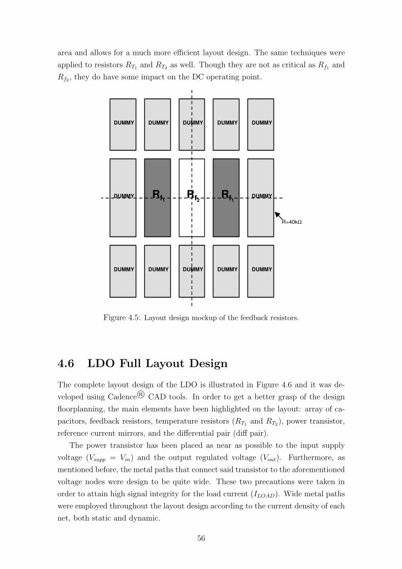
area and allows for a much more efficient layout design. The same techniques were
applied to resistors RT1 and RT2 as well. Though they are not as critical as Rf1 and
Rf2 , they do have some impact on the DC operating point.
Rf2
R=40kΩ
Rf1Rf1
DUMMY DUMMY
DUMMY DUMMY DUMMY DUMMY DUMMY
DUMMYDUMMYDUMMYDUMMYDUMMY
Figure 4.5: Layout design mockup of the feedback resistors.
4.6 LDO Full Layout Design
The complete layout design of the LDO is illustrated in Figure 4.6 and it was de-
veloped using Cadence R© CAD tools. In order to get a better grasp of the design
floorplanning, the main elements have been highlighted on the layout: array of ca-
pacitors, feedback resistors, temperature resistors (RT1 and RT2), power transistor,
reference current mirrors, and the differential pair (diff pair).
The power transistor has been placed as near as possible to the input supply
voltage (Vsupp = Vin) and the output regulated voltage (Vout). Furthermore, as
mentioned before, the metal paths that connect said transistor to the aforementioned
voltage nodes were design to be quite wide. These two precautions were taken in
order to attain high signal integrity for the load current (ILOAD). Wide metal paths
were employed throughout the layout design according to the current density of each
net, both static and dynamic.
56
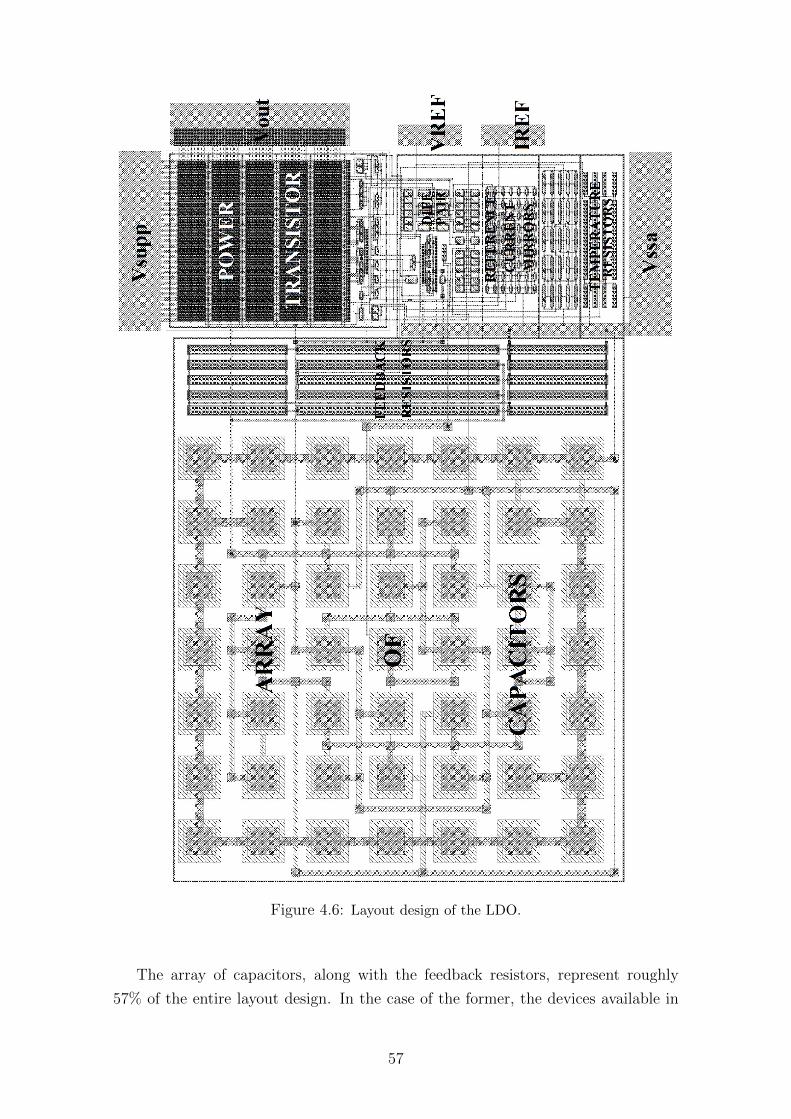
Figure 4.6: Layout design of the LDO.
The array of capacitors, along with the feedback resistors, represent roughly
57% of the entire layout design. In the case of the former, the devices available in
57
the PDK were implemented using the top layers. The top layer has a much larger
minimum width than the rest of them, which derived in a considerably large layout
specially due to the complex internal routing of the array. The feedback resistors
were implemented by poly-resistors, which tend to be quite large as well for values
surpassing 10 kΩ.
There are several guard rings throughout the layout design. Nevertheless, the
main guard rings are the ones that separate the P-type devices from the N-type
devices. The former is connected to Vsupp and the latter to Vssa. The other guard
rings distribuited within the two main ones are placed in order to maintain a low
source to substrate distance for all devices.
Techniques such as common centroid and interdigitation were performed on most
of the remaining current mirrors within the LDO. This ensures a high resiliance to
gradient variations, which are usually present in the fabrication process.
The final die are was of 295.25 µm × 209.57 µm = 0.062 mm2. It is worth
mentioning that the power transistor - which usually takes up at least 33% in most
LDO layout designs - only takes up aroud 8% of the entire area in this particular
design. This means that the techniques employed in the topology and architecture
of the LDO, combined with the ones used in the layout design, allowed for a much
more efficient use of die area.
58
Chapter 5
Simulations Results
The LDO layout design was extracted and simulated on the Cadence R© Framework.
The data was later processed on Matlab R© for a better visualization. The post-layout
simulations were divided into seven types of analyses:
• Steady-State Response: Covers the DC response of the LDO.
• Stability: Shows the open-loop frequency response of the LDO.
• Power Supply Rejection Ratio: Presents the input voltage spuria attenu-
ation throughout the frequency spectrum.
• Load Transient Response: Illustrates the LDO response to sudden full
range load current variations.
• Load Regulation: Quantifies the variation of the output voltage throughout
the entire load current range.
• Line Transient Response: Depicts the LDO response to sudden full range
input supply variations.
• Line Regulation: Quantifies the variation of the output voltage throughout
the entire input supply range.
Moreover, each analysis comprises a set of simulations that characterizes the
performance of the LDO. The simulations chosen were the following:
• Nominal Performance: Verifies the behavior of the LDO at normal condi-
tions (ambient temperature of 27C).
• Temperature Sweep: Revises the behavior of the LDO within the industrial
temperature range (from -40C to 85C).
• Monte Carlo Analysis: Demonstrates the behavior of the LDO when expe-
riencing random fabrication process imperfections (200 samples).
59
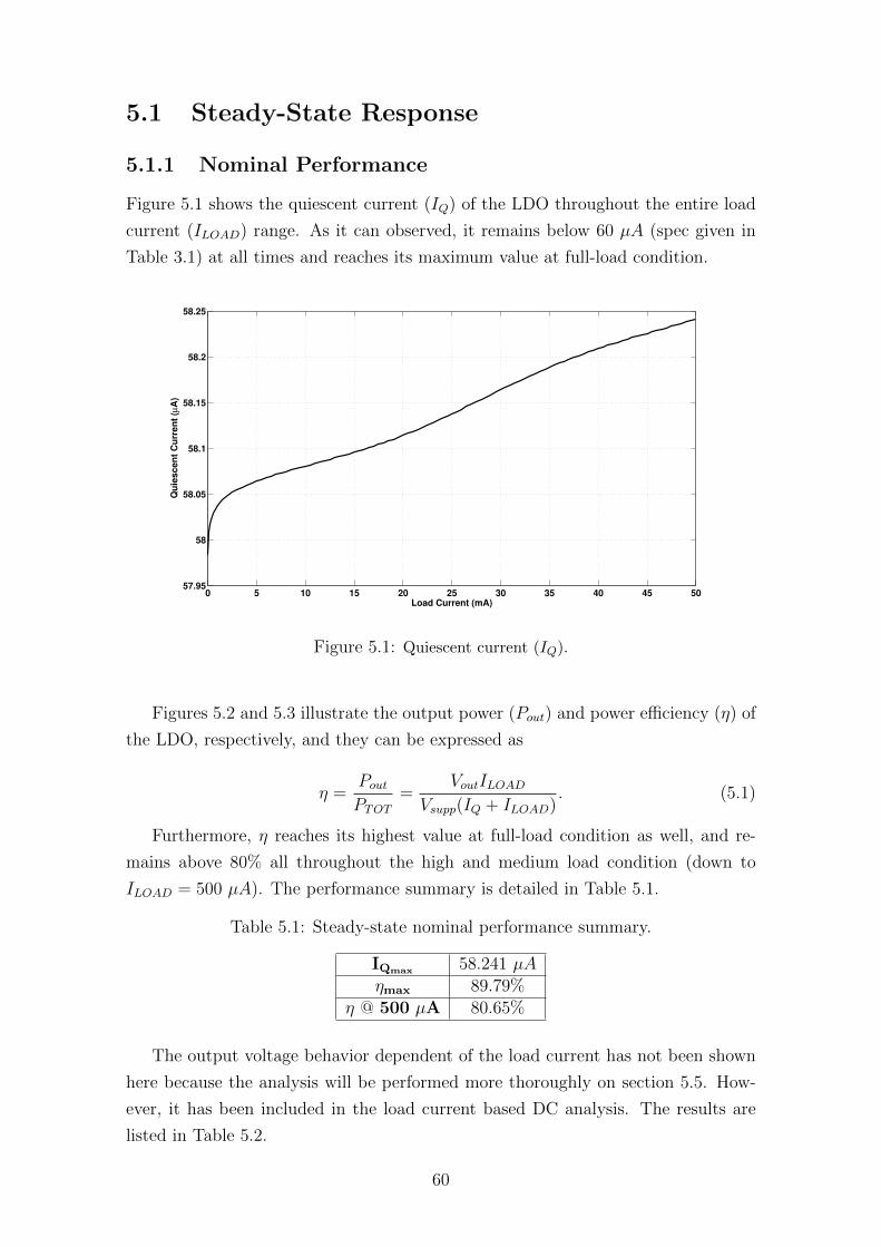
5.1 Steady-State Response
5.1.1 Nominal Performance
Figure 5.1 shows the quiescent current (IQ) of the LDO throughout the entire load
current (ILOAD) range. As it can observed, it remains below 60 µA (spec given in
Table 3.1) at all times and reaches its maximum value at full-load condition.
0 5 10 15 20 25 30 35 40 45 5057.95
58
58.05
58.1
58.15
58.2
58.25
Qu
iescen
t C
urr
en
t (µ
A)
Load Current (mA)
Figure 5.1: Quiescent current (IQ).
Figures 5.2 and 5.3 illustrate the output power (Pout) and power efficiency (η) of
the LDO, respectively, and they can be expressed as
η =PoutPTOT
=VoutILOAD
Vsupp(IQ + ILOAD). (5.1)
Furthermore, η reaches its highest value at full-load condition as well, and re-
mains above 80% all throughout the high and medium load condition (down to
ILOAD = 500 µA). The performance summary is detailed in Table 5.1.
Table 5.1: Steady-state nominal performance summary.
IQmax 58.241 µAηmax 89.79%
η @ 500 µA 80.65%
The output voltage behavior dependent of the load current has not been shown
here because the analysis will be performed more thoroughly on section 5.5. How-
ever, it has been included in the load current based DC analysis. The results are
listed in Table 5.2.
60
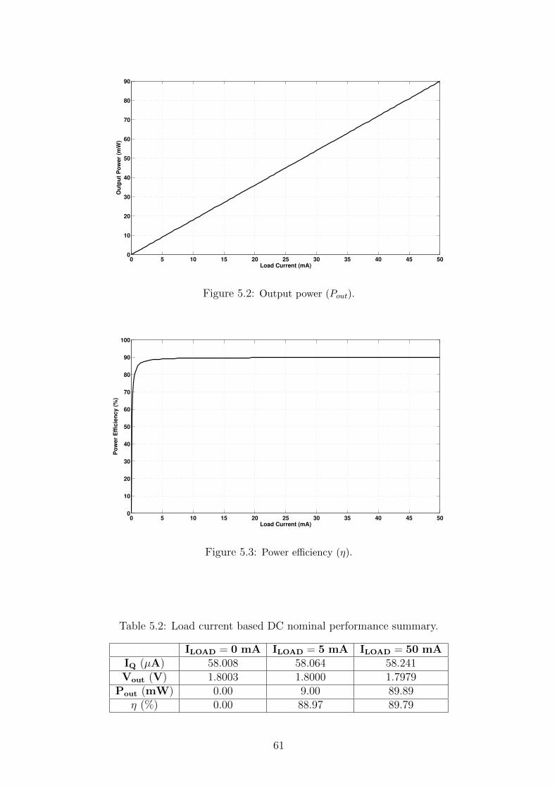
0 5 10 15 20 25 30 35 40 45 500
10
20
30
40
50
60
70
80
90
Ou
tpu
t P
ow
er
(mW
)
Load Current (mA)
Figure 5.2: Output power (Pout).
0 5 10 15 20 25 30 35 40 45 500
10
20
30
40
50
60
70
80
90
100
Po
wer
Eff
icie
ncy (
%)
Load Current (mA)
Figure 5.3: Power efficiency (η).
Table 5.2: Load current based DC nominal performance summary.
ILOAD = 0 mA ILOAD = 5 mA ILOAD = 50 mAIQ (µA) 58.008 58.064 58.241Vout (V) 1.8003 1.8000 1.7979
Pout (mW) 0.00 9.00 89.89η (%) 0.00 88.97 89.79
61
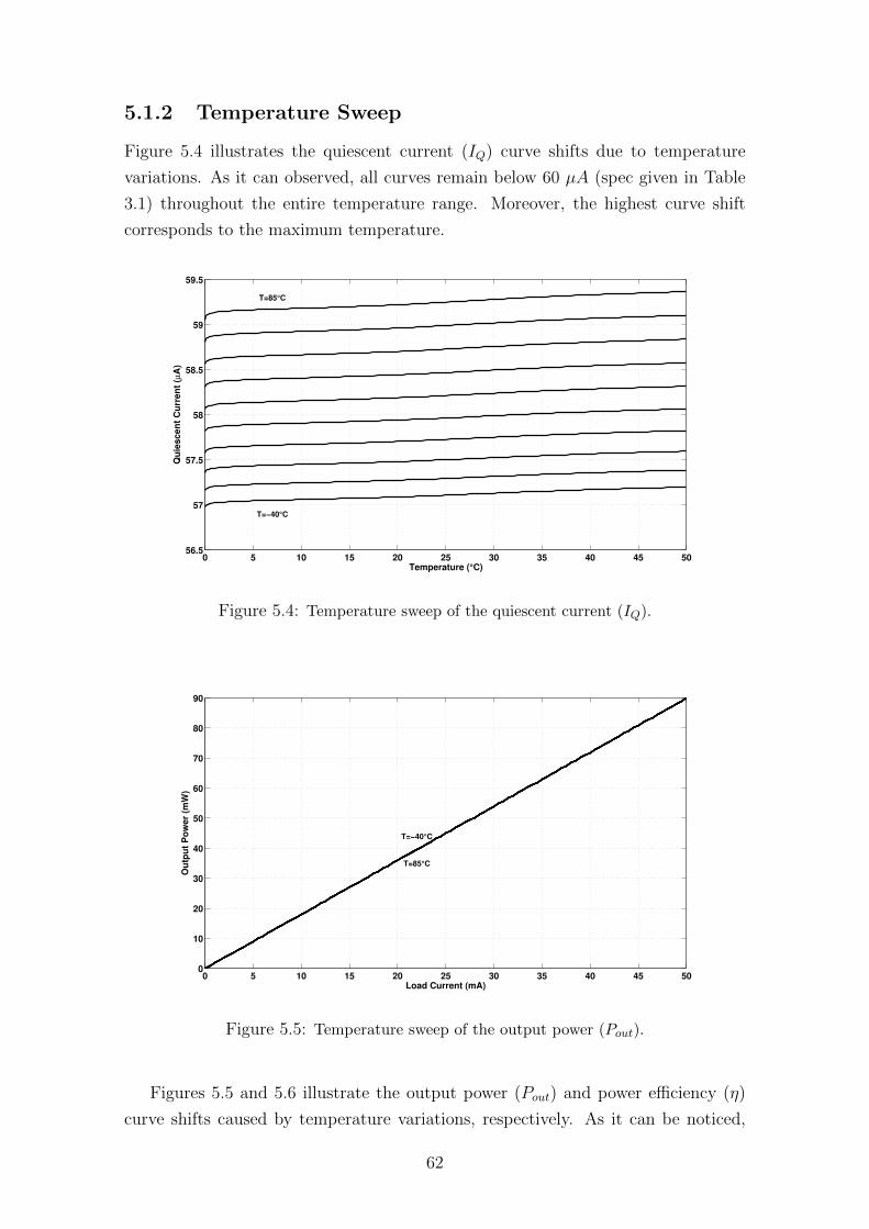
5.1.2 Temperature Sweep
Figure 5.4 illustrates the quiescent current (IQ) curve shifts due to temperature
variations. As it can observed, all curves remain below 60 µA (spec given in Table
3.1) throughout the entire temperature range. Moreover, the highest curve shift
corresponds to the maximum temperature.
0 5 10 15 20 25 30 35 40 45 5056.5
57
57.5
58
58.5
59
59.5
Qu
iescen
t C
urr
en
t (µ
A)
Temperature (°C)
T=85°C
T=−40°C
Figure 5.4: Temperature sweep of the quiescent current (IQ).
0 5 10 15 20 25 30 35 40 45 500
10
20
30
40
50
60
70
80
90
Ou
tpu
t P
ow
er
(mW
)
Load Current (mA)
T=−40°C
T=85°C
Figure 5.5: Temperature sweep of the output power (Pout).
Figures 5.5 and 5.6 illustrate the output power (Pout) and power efficiency (η)
curve shifts caused by temperature variations, respectively. As it can be noticed,
62
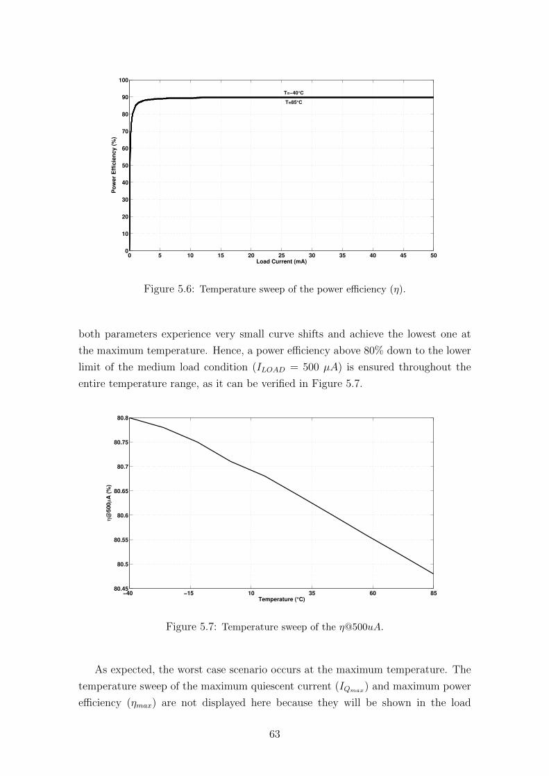
0 5 10 15 20 25 30 35 40 45 500
10
20
30
40
50
60
70
80
90
100
Po
wer
Eff
icie
ncy (
%)
Load Current (mA)
T=−40°C
T=85°C
Figure 5.6: Temperature sweep of the power efficiency (η).
both parameters experience very small curve shifts and achieve the lowest one at
the maximum temperature. Hence, a power efficiency above 80% down to the lower
limit of the medium load condition (ILOAD = 500 µA) is ensured throughout the
entire temperature range, as it can be verified in Figure 5.7.
−40 −15 10 35 60 8580.45
80.5
80.55
80.6
80.65
80.7
80.75
80.8
η@
500
µA
(%
)
Temperature (°C)
Figure 5.7: Temperature sweep of the η@500uA.
As expected, the worst case scenario occurs at the maximum temperature. The
temperature sweep of the maximum quiescent current (IQmax) and maximum power
efficiency (ηmax) are not displayed here because they will be shown in the load
63
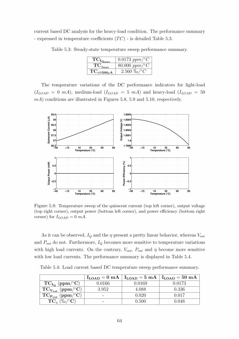
current based DC analysis for the heavy-load condition. The performance summary
- expressed in temperature coefficients (TC) - is detailed Table 5.3.
Table 5.3: Steady-state temperature sweep performance summary.
TCIQmax0.0173 ppm/C
TCηmax 80.000 ppm/CTCη@500µA 2.560 h/C
The temperature variations of the DC performance indicators for light-load
(ILOAD = 0 mA), medium-load (ILOAD = 5 mA) and heavy-load (ILOAD = 50
mA) conditions are illustrated in Figures 5.8, 5.9 and 5.10, respectively.
−40 −15 10 35 60 8556.5
57
57.5
58
58.5
59
59.5
Qu
iescen
t C
urr
en
t (µ
A)
Temperature (°C)−40 −15 10 35 60 85
1.7999
1.8
1.8001
1.8002
1.8003
1.8004
1.8005
Ou
tpu
t V
olt
ag
e (
V)
Temperature (°C)
−40 −15 10 35 60 85−1
−0.5
0
0.5
1
Ou
tpu
t P
ow
er
(mW
)
Temperature (°C)−40 −15 10 35 60 85−1
−0.5
0
0.5
1
Po
wer
Eff
icie
ncy (
%)
Temperature (°C)
Figure 5.8: Temperature sweep of the quiescent current (top left corner), output voltage(top right corner), output power (bottom left corner), and power efficiency (bottom rightcorner) for ILOAD = 0 mA.
As it can be observed, IQ and the η present a pretty linear behavior, whereas Vout
and Pout do not. Furthermore, IQ becomes more sensitive to temperature variations
with high load currents. On the contrary, Vout, Pout and η become more sensitive
with low load currents. The performance summary is displayed in Table 5.4.
Table 5.4: Load current based DC temperature sweep performance summary.
ILOAD = 0 mA ILOAD = 5 mA ILOAD = 50 mATCIQ (ppm/C) 0.0166 0.0169 0.0173
TCVout (ppm/C) 3.952 4.088 0.336TCPout (ppm/C) - 0.020 0.017
TCη (h/C) - 0.500 0.048
64
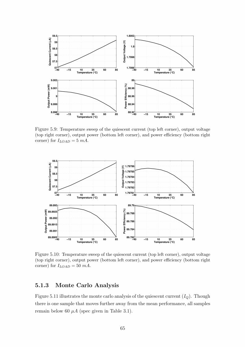
−40 −15 10 35 60 8557
57.5
58
58.5
59
59.5
Qu
iescen
t C
urr
en
t (µ
A)
Temperature (°C)−40 −15 10 35 60 85
1.7996
1.7998
1.8
1.8002
Ou
tpu
t V
olt
ag
e (
V)
Temperature (°C)
−40 −15 10 35 60 858.998
8.999
9
9.001
9.002
Ou
tpu
t P
ow
er
(mW
)
Temperature (°C)−40 −15 10 35 60 85
88.92
88.94
88.96
88.98
89
Po
wer
Eff
icie
ncy (
%)
Temperature (°C)
Figure 5.9: Temperature sweep of the quiescent current (top left corner), output voltage(top right corner), output power (bottom left corner), and power efficiency (bottom rightcorner) for ILOAD = 5 mA.
−40 −15 10 35 60 8557
57.5
58
58.5
59
59.5
Qu
iescen
t C
urr
en
t (µ
A)
Temperature (°C)−40 −15 10 35 60 85
1.79781
1.79782
1.79783
1.79784
1.79785
1.79786
Ou
tpu
t V
olt
ag
e (
V)
Temperature (°C)
−40 −15 10 35 60 8589.8905
89.891
89.8915
89.892
89.8925
89.893
Ou
tpu
t P
ow
er
(mW
)
Temperature (°C)−40 −15 10 35 60 85
89.782
89.784
89.786
89.788
89.79
Po
wer
Eff
icie
ncy (
%)
Temperature (°C)
Figure 5.10: Temperature sweep of the quiescent current (top left corner), output voltage(top right corner), output power (bottom left corner), and power efficiency (bottom rightcorner) for ILOAD = 50 mA.
5.1.3 Monte Carlo Analysis
Figure 5.11 illustrates the monte carlo analysis of the quiescent current (IQ). Though
there is one sample that moves further away from the mean performance, all samples
remain below 60 µA (spec given in Table 3.1).
65
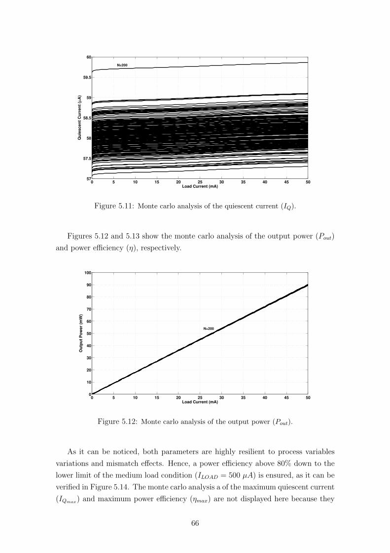
0 5 10 15 20 25 30 35 40 45 5057
57.5
58
58.5
59
59.5
60
Qu
iescen
t C
urr
en
t (µ
A)
Load Current (mA)
N=200
Figure 5.11: Monte carlo analysis of the quiescent current (IQ).
Figures 5.12 and 5.13 show the monte carlo analysis of the output power (Pout)
and power efficiency (η), respectively.
0 5 10 15 20 25 30 35 40 45 500
10
20
30
40
50
60
70
80
90
100
Ou
tpu
t P
ow
er
(mW
)
Load Current (mA)
N=200
Figure 5.12: Monte carlo analysis of the output power (Pout).
As it can be noticed, both parameters are highly resilient to process variables
variations and mismatch effects. Hence, a power efficiency above 80% down to the
lower limit of the medium load condition (ILOAD = 500 µA) is ensured, as it can be
verified in Figure 5.14. The monte carlo analysis a of the maximum quiescent current
(IQmax) and maximum power efficiency (ηmax) are not displayed here because they
66
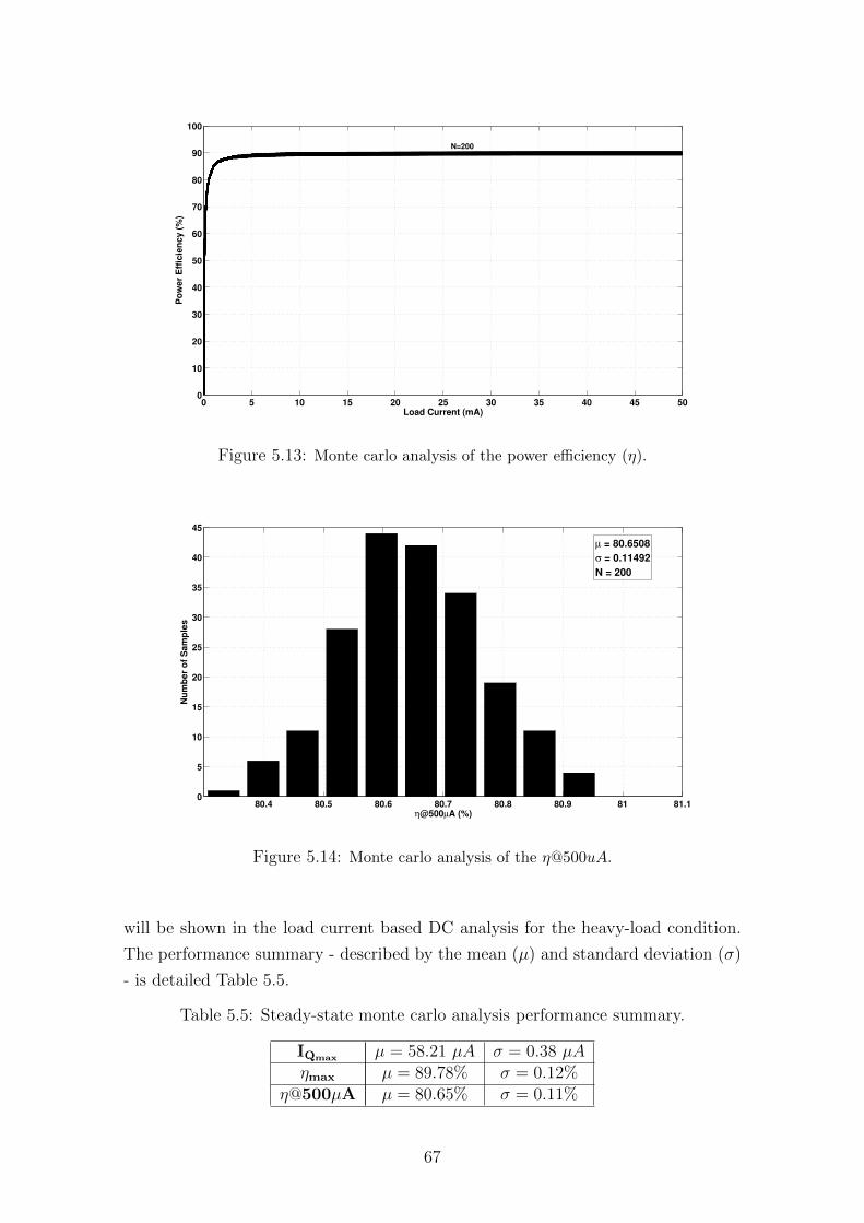
0 5 10 15 20 25 30 35 40 45 500
10
20
30
40
50
60
70
80
90
100
Po
wer
Eff
icie
ncy (
%)
Load Current (mA)
N=200
Figure 5.13: Monte carlo analysis of the power efficiency (η).
80.4 80.5 80.6 80.7 80.8 80.9 81 81.10
5
10
15
20
25
30
35
40
45
µ = 80.6508
σ = 0.11492
N = 200
Nu
mb
er
of
Sam
ple
s
η@500µA (%)
Figure 5.14: Monte carlo analysis of the η@500uA.
will be shown in the load current based DC analysis for the heavy-load condition.
The performance summary - described by the mean (µ) and standard deviation (σ)
- is detailed Table 5.5.
Table 5.5: Steady-state monte carlo analysis performance summary.
IQmax µ = 58.21 µA σ = 0.38 µAηmax µ = 89.78% σ = 0.12%
η@500µA µ = 80.65% σ = 0.11%
67
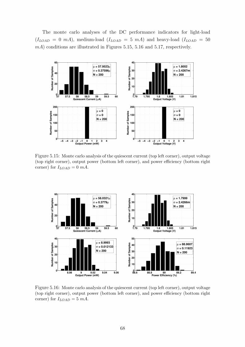
The monte carlo analyses of the DC performance indicators for light-load
(ILOAD = 0 mA), medium-load (ILOAD = 5 mA) and heavy-load (ILOAD = 50
mA) conditions are illustrated in Figures 5.15, 5.16 and 5.17, respectively.
57 57.5 58 58.5 59 59.5 600
20
40
60
µ = 57.9523µ
σ = 0.37596µ
N = 200
Nu
mb
er
of
Sam
ple
s
Quiescent Current (µA)1.79 1.795 1.8 1.805 1.81 1.8150
10
20
30
40
µ = 1.8002
σ = 2.4267m
N = 200
Nu
mb
er
of
Sam
ple
s
Output Voltage (V)
−5 −4 −3 −2 −1 0 1 2 3 40
50
100
150
200
µ = 0
σ = 0
N = 200
Nu
mb
er
of
Sam
ple
s
Output Power (mW)−5 −4 −3 −2 −1 0 1 2 3 4
0
50
100
150
200
µ = 0
σ = 0
N = 200
Nu
mb
er
of
Sam
ple
s
Output Voltage (V)
Figure 5.15: Monte carlo analysis of the quiescent current (top left corner), output voltage(top right corner), output power (bottom left corner), and power efficiency (bottom rightcorner) for ILOAD = 0 mA.
57 57.5 58 58.5 59 59.5 600
20
40
60
µ = 58.0321µ
σ = 0.3779µ
N = 200
Nu
mb
er
of
Sam
ple
s
Quiescent Current (µA)1.79 1.795 1.8 1.805 1.81 1.8150
10
20
30
40
µ = 1.7999
σ = 2.4266m
N = 200
Nu
mb
er
of
Sam
ple
s
Output Voltage (V)
8.98 9 9.02 9.04 9.060
10
20
30
40
µ = 8.9993
σ = 0.012133
N = 200
Nu
mb
er
of
Sam
ple
s
Output Power (mW)88.6 88.8 89 89.2 89.40
10
20
30
40
50
µ = 88.9607
σ = 0.11923
N = 200
Nu
mb
er
of
Sam
ple
s
Power Efficiency (%)
Figure 5.16: Monte carlo analysis of the quiescent current (top left corner), output voltage(top right corner), output power (bottom left corner), and power efficiency (bottom rightcorner) for ILOAD = 5 mA.
68
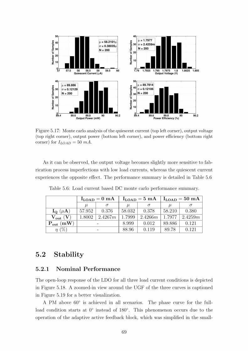
57 57.5 58 58.5 59 59.5 600
10
20
30
40
50
µ = 58.2101µ
σ = 0.38035µ
N = 200N
um
ber
of
Sam
ple
s
Quiescent Current (µA)1.79 1.7925 1.795 1.7975 1.8 1.8025 1.8050
10
20
30
40
µ = 1.7977
σ = 2.4259m
N = 200
Nu
mb
er
of
Sam
ple
s
Output Voltage (V)
89.4 89.6 89.8 90 90.20
10
20
30
40
µ = 89.886
σ = 0.12129
N = 200
Nu
mb
er
of
Sam
ple
s
Output Power (mW)89.4 89.6 89.8 90 90.20
10
20
30
40
50
µ = 89.7814
σ = 0.12106
N = 200
Nu
mb
er
of
Sam
ple
s
Power Efficiency (%)
Figure 5.17: Monte carlo analysis of the quiescent current (top left corner), output voltage(top right corner), output power (bottom left corner), and power efficiency (bottom rightcorner) for ILOAD = 50 mA.
As it can be observed, the output voltage becomes slightly more sensitive to fab-
rication process imperfections with low load currents, whereas the quiescent current
experiences the opposite effect. The performance summary is detailed in Table 5.6
Table 5.6: Load current based DC monte carlo performance summary.
ILOAD = 0 mA ILOAD = 5 mA ILOAD = 50 mAµ σ µ σ µ σ
IQ (µA) 57.952 0.376 58.032 0.378 58.210 0.380Vout (V) 1.8002 2.4267m 1.7999 2.4266m 1.7977 2.4259m
Pout (mW) - 8.999 0.012 89.886 0.121η (%) - 88.96 0.119 89.78 0.121
5.2 Stability
5.2.1 Nominal Performance
The open-loop response of the LDO for all three load current conditions is depicted
in Figure 5.18. A zoomed-in view around the UGF of the three curves is captioned
in Figure 5.19 for a better visualization.
A PM above 60 is achieved in all scenarios. The phase curve for the full-
load condition starts at 0 instead of 180. This phenomenon occurs due to the
operation of the adaptive active feedback block, which was simplified in the small-
69
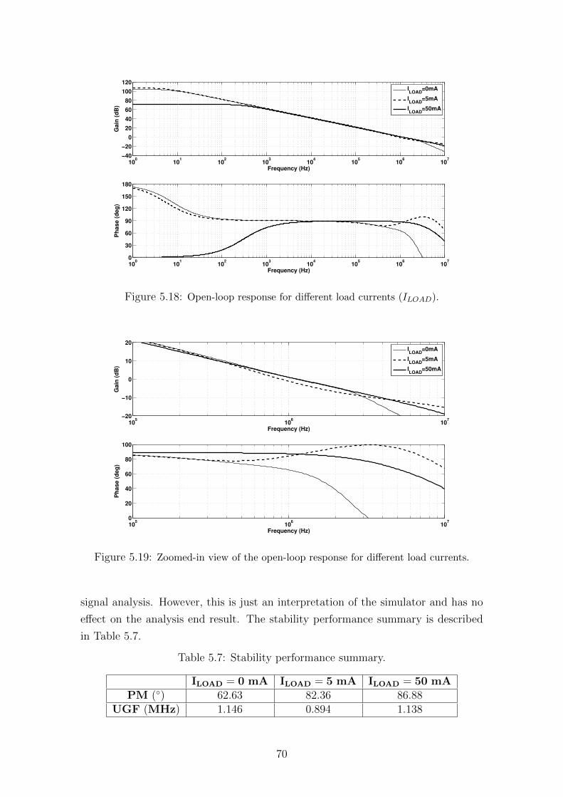
100
101
102
103
104
105
106
107
−40
−20
0
20
40
60
80
100
120
Gain
(d
B)
Frequency (Hz)
ILOAD
=0mA
ILOAD
=5mA
ILOAD
=50mA
100
101
102
103
104
105
106
107
0
30
60
90
120
150
180
Ph
ase (
deg
)
Frequency (Hz)
Figure 5.18: Open-loop response for different load currents (ILOAD).
105
106
107
−20
−10
0
10
20
Gain
(d
B)
Frequency (Hz)
ILOAD
=0mA
ILOAD
=5mA
ILOAD
=50mA
105
106
107
0
20
40
60
80
100
Ph
ase (
deg
)
Frequency (Hz)
Figure 5.19: Zoomed-in view of the open-loop response for different load currents.
signal analysis. However, this is just an interpretation of the simulator and has no
effect on the analysis end result. The stability performance summary is described
in Table 5.7.
Table 5.7: Stability performance summary.
ILOAD = 0 mA ILOAD = 5 mA ILOAD = 50 mAPM () 62.63 82.36 86.88
UGF (MHz) 1.146 0.894 1.138
70
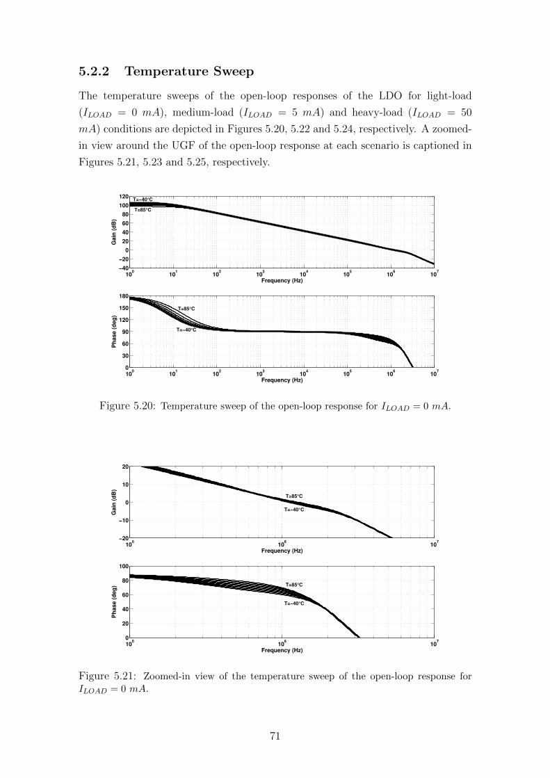
5.2.2 Temperature Sweep
The temperature sweeps of the open-loop responses of the LDO for light-load
(ILOAD = 0 mA), medium-load (ILOAD = 5 mA) and heavy-load (ILOAD = 50
mA) conditions are depicted in Figures 5.20, 5.22 and 5.24, respectively. A zoomed-
in view around the UGF of the open-loop response at each scenario is captioned in
Figures 5.21, 5.23 and 5.25, respectively.
100
101
102
103
104
105
106
107
−40
−20
0
20
40
60
80
100
120
Gain
(d
B)
Frequency (Hz)
T=−40°C
T=85°C
100
101
102
103
104
105
106
107
0
30
60
90
120
150
180
Ph
ase (
deg
)
Frequency (Hz)
T=85°C
T=−40°C
Figure 5.20: Temperature sweep of the open-loop response for ILOAD = 0 mA.
105
106
107
−20
−10
0
10
20
Gain
(d
B)
Frequency (Hz)
T=85°C
T=−40°C
105
106
107
0
20
40
60
80
100
Ph
ase (
deg
)
Frequency (Hz)
T=85°C
T=−40°C
Figure 5.21: Zoomed-in view of the temperature sweep of the open-loop response forILOAD = 0 mA.
71
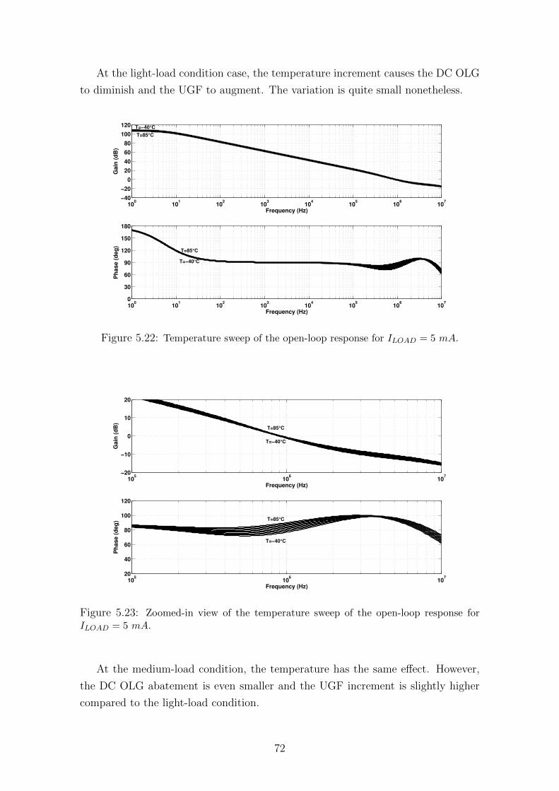
At the light-load condition case, the temperature increment causes the DC OLG
to diminish and the UGF to augment. The variation is quite small nonetheless.
100
101
102
103
104
105
106
107
−40
−20
0
20
40
60
80
100
120
Gain
(d
B)
Frequency (Hz)
T=−40°C
T=85°C
100
101
102
103
104
105
106
107
0
30
60
90
120
150
180
Ph
ase (
deg
)
Frequency (Hz)
T=85°C
T=−40°C
Figure 5.22: Temperature sweep of the open-loop response for ILOAD = 5 mA.
105
106
107
−20
−10
0
10
20
Gain
(d
B)
Frequency (Hz)
T=85°C
T=−40°C
105
106
107
20
40
60
80
100
120
Ph
ase (
deg
)
Frequency (Hz)
T=85°C
T=−40°C
Figure 5.23: Zoomed-in view of the temperature sweep of the open-loop response forILOAD = 5 mA.
At the medium-load condition, the temperature has the same effect. However,
the DC OLG abatement is even smaller and the UGF increment is slightly higher
compared to the light-load condition.
72
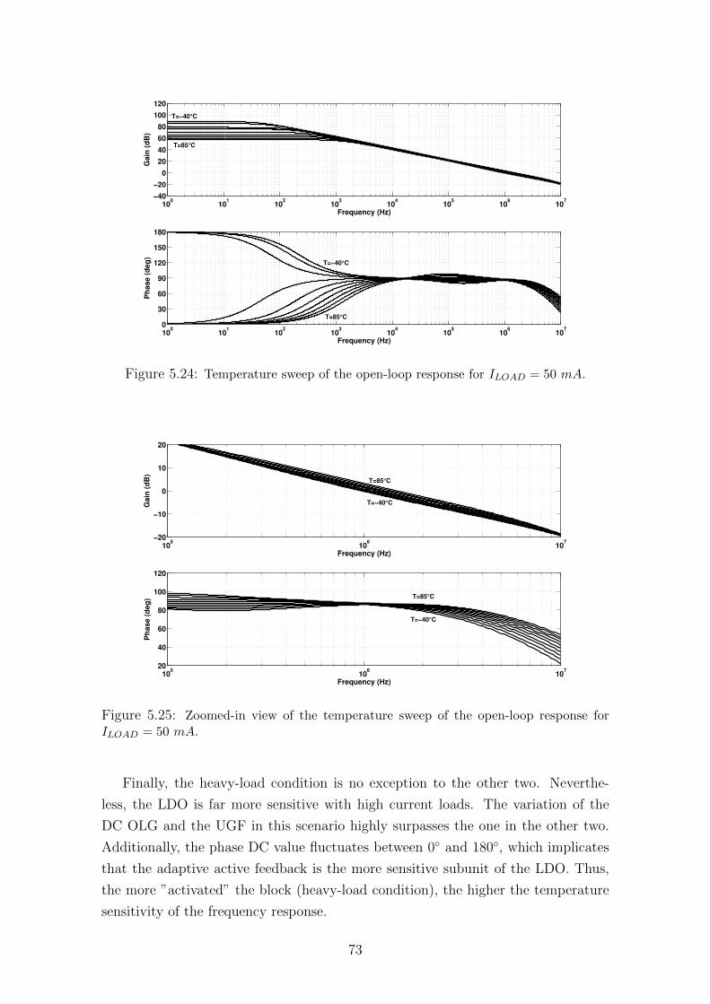
100
101
102
103
104
105
106
107
−40
−20
0
20
40
60
80
100
120
Gain
(d
B)
Frequency (Hz)
T=−40°C
T=85°C
100
101
102
103
104
105
106
107
0
30
60
90
120
150
180
Ph
ase (
deg
)
Frequency (Hz)
T=−40°C
T=85°C
Figure 5.24: Temperature sweep of the open-loop response for ILOAD = 50 mA.
105
106
107
−20
−10
0
10
20
Gain
(d
B)
Frequency (Hz)
T=85°C
T=−40°C
105
106
107
20
40
60
80
100
120
Ph
ase (
deg
)
Frequency (Hz)
T=85°C
T=−40°C
Figure 5.25: Zoomed-in view of the temperature sweep of the open-loop response forILOAD = 50 mA.
Finally, the heavy-load condition is no exception to the other two. Neverthe-
less, the LDO is far more sensitive with high current loads. The variation of the
DC OLG and the UGF in this scenario highly surpasses the one in the other two.
Additionally, the phase DC value fluctuates between 0 and 180, which implicates
that the adaptive active feedback is the more sensitive subunit of the LDO. Thus,
the more ”activated” the block (heavy-load condition), the higher the temperature
sensitivity of the frequency response.
73
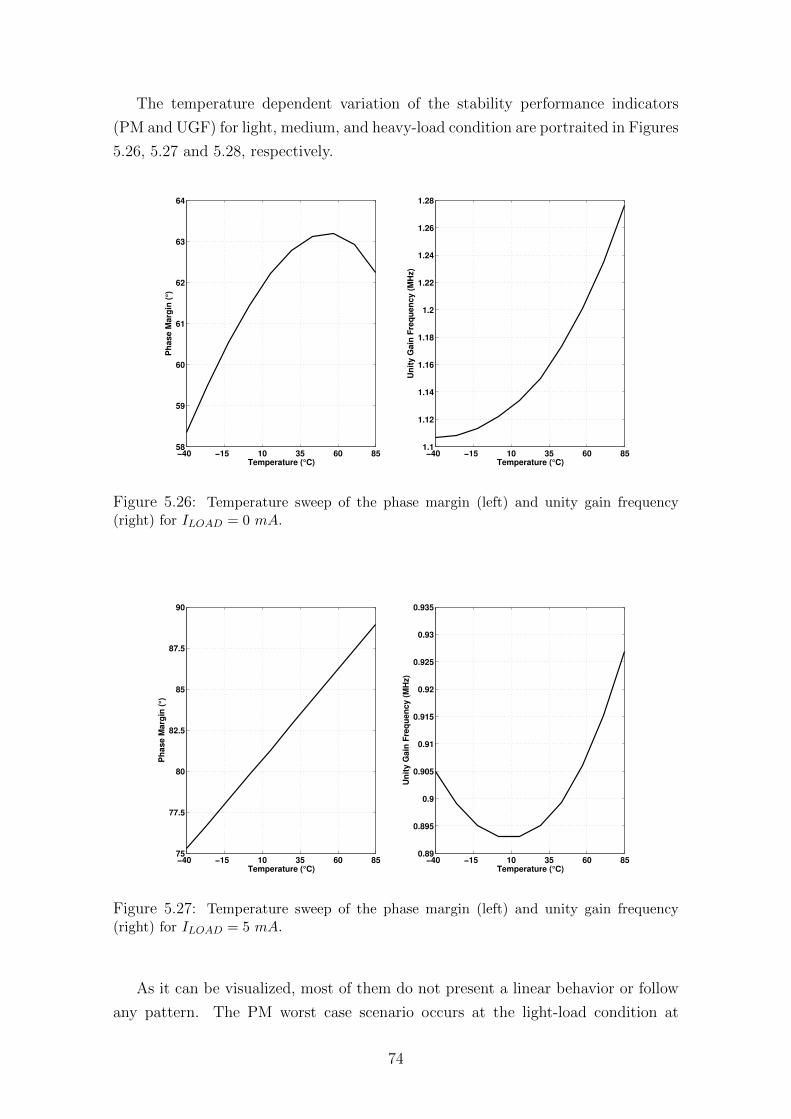
The temperature dependent variation of the stability performance indicators
(PM and UGF) for light, medium, and heavy-load condition are portraited in Figures
5.26, 5.27 and 5.28, respectively.
−40 −15 10 35 60 8558
59
60
61
62
63
64
Ph
ase M
arg
in (
°)
Temperature (°C)−40 −15 10 35 60 85
1.1
1.12
1.14
1.16
1.18
1.2
1.22
1.24
1.26
1.28
Un
ity G
ain
Fre
qu
en
cy (
MH
z)
Temperature (°C)
Figure 5.26: Temperature sweep of the phase margin (left) and unity gain frequency(right) for ILOAD = 0 mA.
−40 −15 10 35 60 8575
77.5
80
82.5
85
87.5
90
Ph
ase M
arg
in (
°)
Temperature (°C)−40 −15 10 35 60 85
0.89
0.895
0.9
0.905
0.91
0.915
0.92
0.925
0.93
0.935
Un
ity G
ain
Fre
qu
en
cy (
MH
z)
Temperature (°C)
Figure 5.27: Temperature sweep of the phase margin (left) and unity gain frequency(right) for ILOAD = 5 mA.
As it can be visualized, most of them do not present a linear behavior or follow
any pattern. The PM worst case scenario occurs at the light-load condition at
74
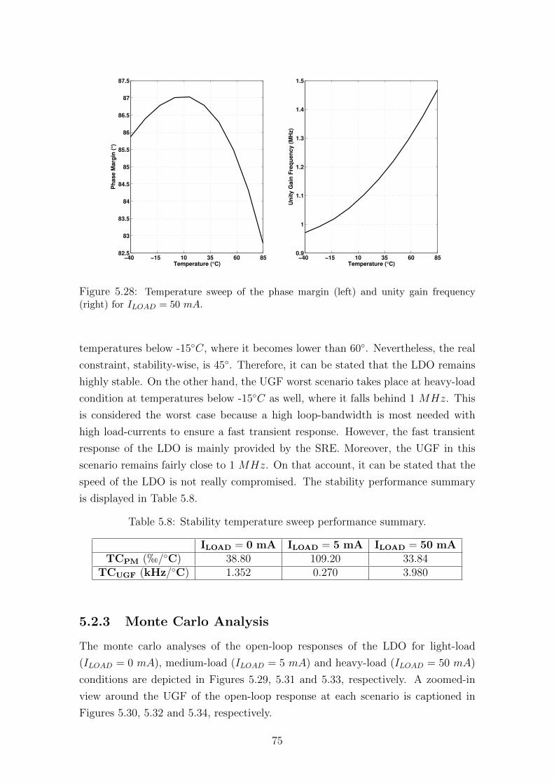
−40 −15 10 35 60 8582.5
83
83.5
84
84.5
85
85.5
86
86.5
87
87.5
Ph
ase M
arg
in (
°)
Temperature (°C)−40 −15 10 35 60 85
0.9
1
1.1
1.2
1.3
1.4
1.5
Un
ity G
ain
Fre
qu
en
cy (
MH
z)
Temperature (°C)
Figure 5.28: Temperature sweep of the phase margin (left) and unity gain frequency(right) for ILOAD = 50 mA.
temperatures below -15C, where it becomes lower than 60. Nevertheless, the real
constraint, stability-wise, is 45. Therefore, it can be stated that the LDO remains
highly stable. On the other hand, the UGF worst scenario takes place at heavy-load
condition at temperatures below -15C as well, where it falls behind 1 MHz. This
is considered the worst case because a high loop-bandwidth is most needed with
high load-currents to ensure a fast transient response. However, the fast transient
response of the LDO is mainly provided by the SRE. Moreover, the UGF in this
scenario remains fairly close to 1 MHz. On that account, it can be stated that the
speed of the LDO is not really compromised. The stability performance summary
is displayed in Table 5.8.
Table 5.8: Stability temperature sweep performance summary.
ILOAD = 0 mA ILOAD = 5 mA ILOAD = 50 mATCPM (h/C) 38.80 109.20 33.84
TCUGF (kHz/C) 1.352 0.270 3.980
5.2.3 Monte Carlo Analysis
The monte carlo analyses of the open-loop responses of the LDO for light-load
(ILOAD = 0 mA), medium-load (ILOAD = 5 mA) and heavy-load (ILOAD = 50 mA)
conditions are depicted in Figures 5.29, 5.31 and 5.33, respectively. A zoomed-in
view around the UGF of the open-loop response at each scenario is captioned in
Figures 5.30, 5.32 and 5.34, respectively.
75
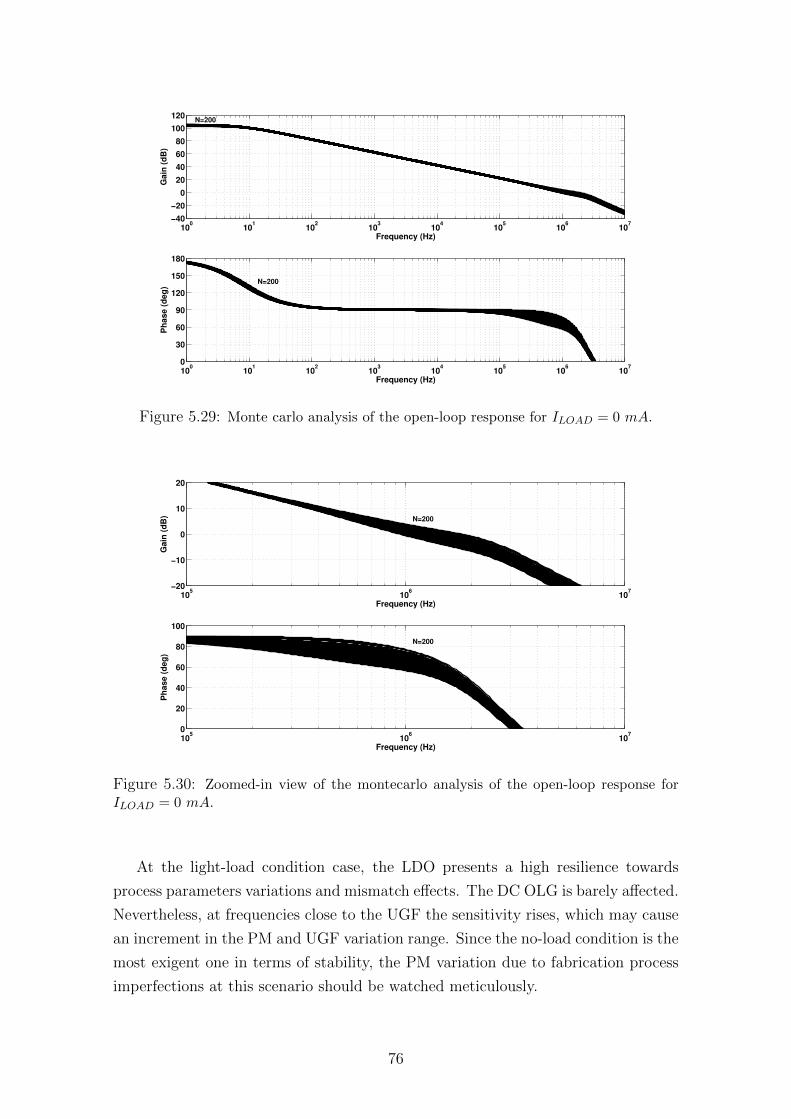
100
101
102
103
104
105
106
107
−40
−20
0
20
40
60
80
100
120
Gain
(d
B)
Frequency (Hz)
N=200
100
101
102
103
104
105
106
107
0
30
60
90
120
150
180
Ph
ase (
deg
)
Frequency (Hz)
N=200
Figure 5.29: Monte carlo analysis of the open-loop response for ILOAD = 0 mA.
105
106
107
−20
−10
0
10
20
Gain
(d
B)
Frequency (Hz)
N=200
105
106
107
0
20
40
60
80
100
Ph
ase (
deg
)
Frequency (Hz)
N=200
Figure 5.30: Zoomed-in view of the montecarlo analysis of the open-loop response forILOAD = 0 mA.
At the light-load condition case, the LDO presents a high resilience towards
process parameters variations and mismatch effects. The DC OLG is barely affected.
Nevertheless, at frequencies close to the UGF the sensitivity rises, which may cause
an increment in the PM and UGF variation range. Since the no-load condition is the
most exigent one in terms of stability, the PM variation due to fabrication process
imperfections at this scenario should be watched meticulously.
76
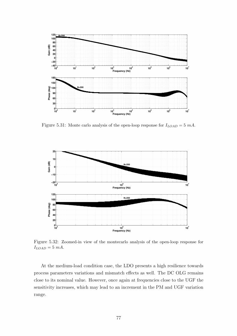
100
101
102
103
104
105
106
107
−40
−20
0
20
40
60
80
100
120
Gain
(d
B)
Frequency (Hz)
N=200
100
101
102
103
104
105
106
107
0
30
60
90
120
150
180
Ph
ase (
deg
)
Frequency (Hz)
N=200
Figure 5.31: Monte carlo analysis of the open-loop response for ILOAD = 5 mA.
105
106
107
−20
−10
0
10
20
Gain
(d
B)
Frequency (Hz)
N=200
105
106
107
0
20
40
60
80
100
120
Ph
ase (
deg
)
Frequency (Hz)
N=200
Figure 5.32: Zoomed-in view of the montecarlo analysis of the open-loop response forILOAD = 5 mA.
At the medium-load condition case, the LDO presents a high resilience towards
process parameters variations and mismatch effects as well. The DC OLG remains
close to its nominal value. However, once again at frequencies close to the UGF the
sensitivity increases, which may lead to an increment in the PM and UGF variation
range.
77
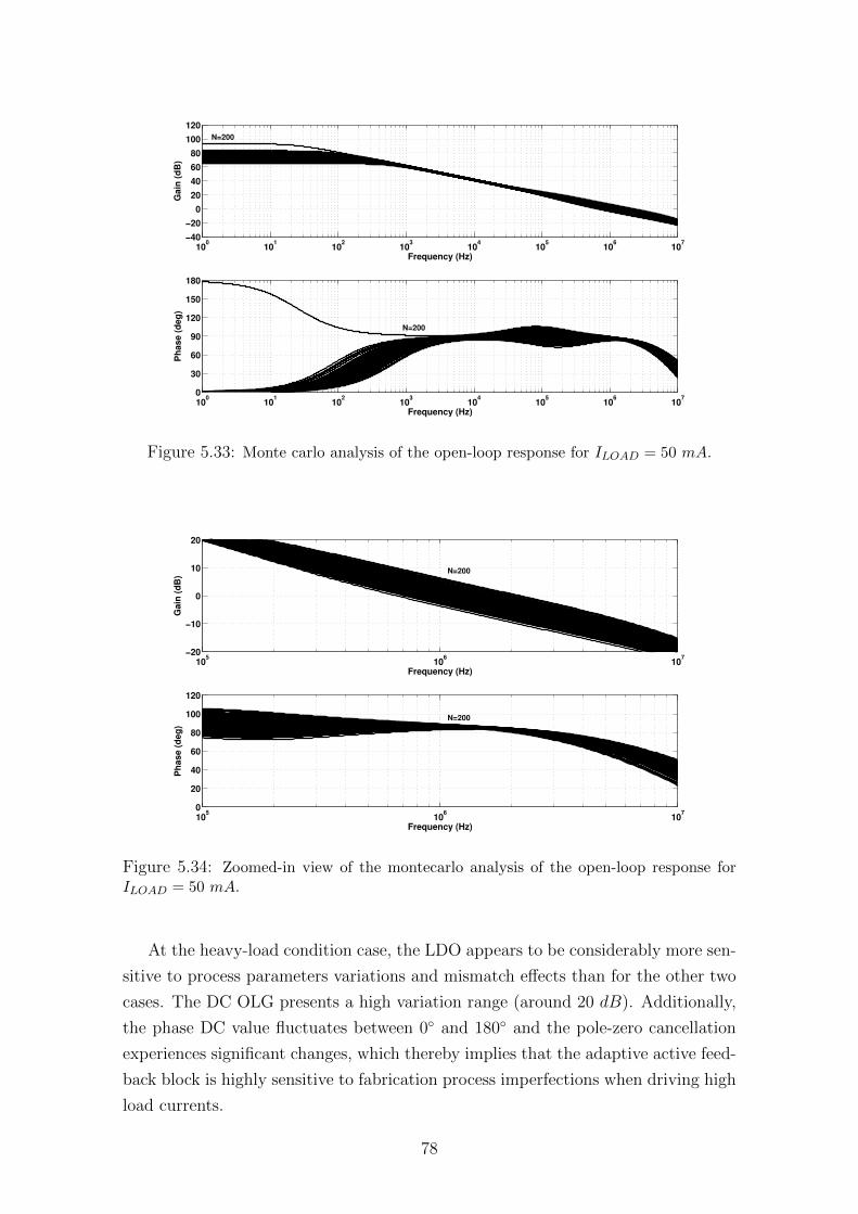
100
101
102
103
104
105
106
107
−40
−20
0
20
40
60
80
100
120
Gain
(d
B)
Frequency (Hz)
N=200
100
101
102
103
104
105
106
107
0
30
60
90
120
150
180
Ph
ase (
deg
)
Frequency (Hz)
N=200
Figure 5.33: Monte carlo analysis of the open-loop response for ILOAD = 50 mA.
105
106
107
−20
−10
0
10
20
Gain
(d
B)
Frequency (Hz)
N=200
105
106
107
0
20
40
60
80
100
120
Ph
ase (
deg
)
Frequency (Hz)
N=200
Figure 5.34: Zoomed-in view of the montecarlo analysis of the open-loop response forILOAD = 50 mA.
At the heavy-load condition case, the LDO appears to be considerably more sen-
sitive to process parameters variations and mismatch effects than for the other two
cases. The DC OLG presents a high variation range (around 20 dB). Additionally,
the phase DC value fluctuates between 0 and 180 and the pole-zero cancellation
experiences significant changes, which thereby implies that the adaptive active feed-
back block is highly sensitive to fabrication process imperfections when driving high
load currents.
78
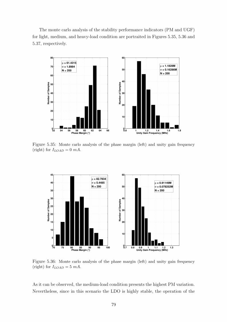
The monte carlo analysis of the stability performance indicators (PM and UGF)
for light, medium, and heavy-load condition are portraited in Figures 5.35, 5.36 and
5.37, respectively.
52 54 56 58 60 62 64 660
10
20
30
40
50
60
70
80
µ = 61.4315
σ = 1.8984
N = 200
Nu
mb
er
of
Sam
ple
s
Phase Margin (°)0.8 1 1.2 1.4 1.6 1.80
10
20
30
40
50
60
µ = 1.1828M
σ = 0.16286M
N = 200
Nu
mb
er
of
Sam
ple
s
Unity Gain Frequency (MHz)
Figure 5.35: Monte carlo analysis of the phase margin (left) and unity gain frequency(right) for ILOAD = 0 mA.
70 75 80 85 90 95 1000
5
10
15
20
25
30
35
40
45
µ = 82.7834
σ = 5.4485
N = 200
Nu
mb
er
of
Sam
ple
s
Phase Margin (°)0.7 0.8 0.9 1 1.1 1.2 1.30
10
20
30
40
50
60
µ = 0.91149M
σ = 0.078252M
N = 200
Nu
mb
er
of
Sam
ple
s
Unity Gain Frequency (MHz)
Figure 5.36: Monte carlo analysis of the phase margin (left) and unity gain frequency(right) for ILOAD = 5 mA.
As it can be observed, the medium-load condition presents the highest PM variation.
Nevertheless, since in this scenario the LDO is highly stable, the operation of the
79
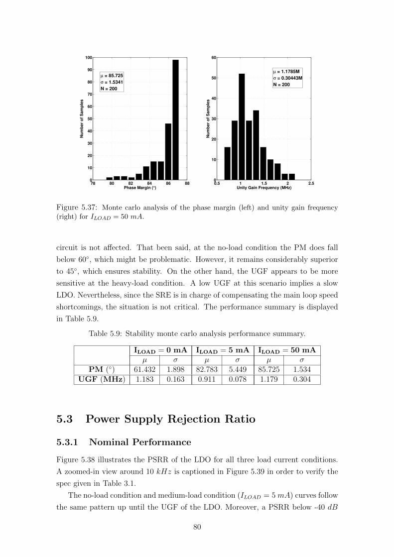
78 80 82 84 86 880
10
20
30
40
50
60
70
80
90
100
µ = 85.725
σ = 1.5341
N = 200
Nu
mb
er
of
Sam
ple
s
Phase Margin (°)0.5 1 1.5 2 2.50
10
20
30
40
50
60
µ = 1.1785M
σ = 0.30443M
N = 200
Nu
mb
er
of
Sam
ple
s
Unity Gain Frequency (MHz)
Figure 5.37: Monte carlo analysis of the phase margin (left) and unity gain frequency(right) for ILOAD = 50 mA.
circuit is not affected. That been said, at the no-load condition the PM does fall
below 60, which might be problematic. However, it remains considerably superior
to 45, which ensures stability. On the other hand, the UGF appears to be more
sensitive at the heavy-load condition. A low UGF at this scenario implies a slow
LDO. Nevertheless, since the SRE is in charge of compensating the main loop speed
shortcomings, the situation is not critical. The performance summary is displayed
in Table 5.9.
Table 5.9: Stability monte carlo analysis performance summary.
ILOAD = 0 mA ILOAD = 5 mA ILOAD = 50 mAµ σ µ σ µ σ
PM () 61.432 1.898 82.783 5.449 85.725 1.534UGF (MHz) 1.183 0.163 0.911 0.078 1.179 0.304
5.3 Power Supply Rejection Ratio
5.3.1 Nominal Performance
Figure 5.38 illustrates the PSRR of the LDO for all three load current conditions.
A zoomed-in view around 10 kHz is captioned in Figure 5.39 in order to verify the
spec given in Table 3.1.
The no-load condition and medium-load condition (ILOAD = 5 mA) curves follow
the same pattern up until the UGF of the LDO. Moreover, a PSRR below -40 dB
80
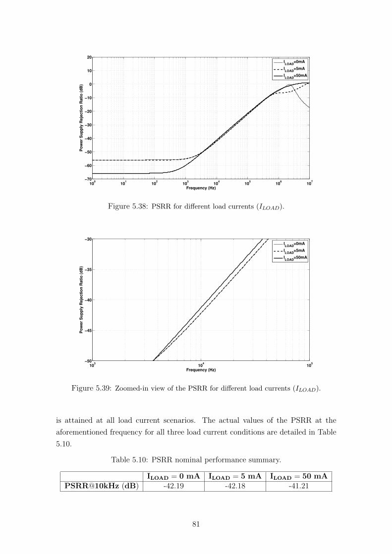
100
101
102
103
104
105
106
107
−70
−60
−50
−40
−30
−20
−10
0
10
20
Po
wer
Su
pp
ly R
eje
cti
on
Rati
o (
dB
)
Frequency (Hz)
ILOAD
=0mA
ILOAD
=5mA
ILOAD
=50mA
Figure 5.38: PSRR for different load currents (ILOAD).
103
104
105
−50
−45
−40
−35
−30
Po
wer
Su
pp
ly R
eje
cti
on
Rati
o (
dB
)
Frequency (Hz)
ILOAD
=0mA
ILOAD
=5mA
ILOAD
=50mA
Figure 5.39: Zoomed-in view of the PSRR for different load currents (ILOAD).
is attained at all load current scenarios. The actual values of the PSRR at the
aforementioned frequency for all three load current conditions are detailed in Table
5.10.
Table 5.10: PSRR nominal performance summary.
ILOAD = 0 mA ILOAD = 5 mA ILOAD = 50 mAPSRR@10kHz (dB) -42.19 -42.18 -41.21
81
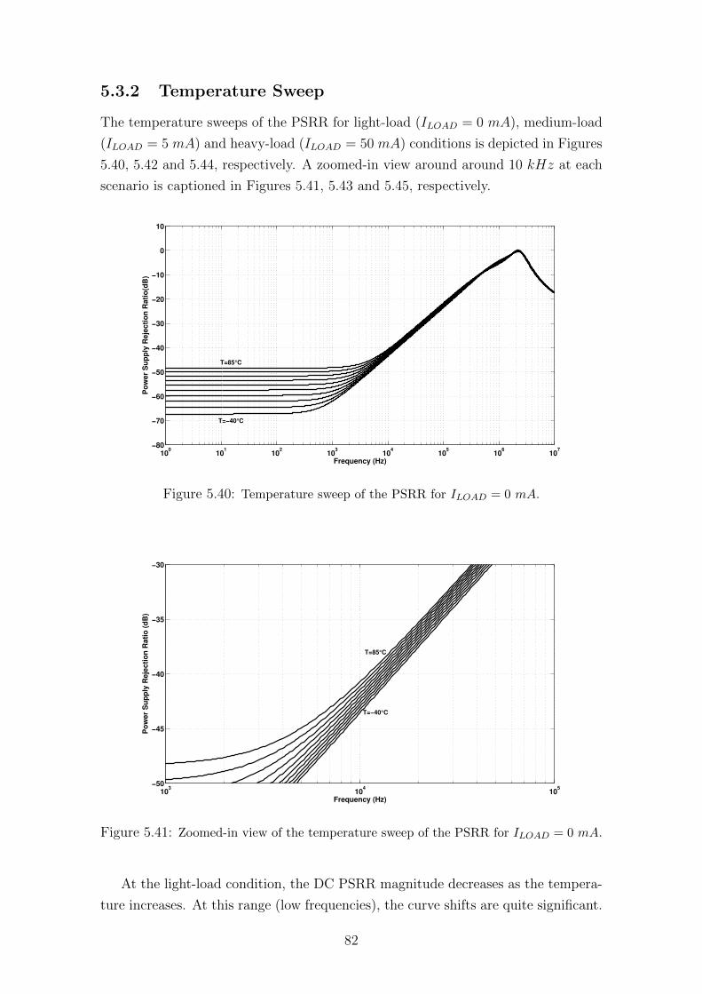
5.3.2 Temperature Sweep
The temperature sweeps of the PSRR for light-load (ILOAD = 0 mA), medium-load
(ILOAD = 5 mA) and heavy-load (ILOAD = 50 mA) conditions is depicted in Figures
5.40, 5.42 and 5.44, respectively. A zoomed-in view around around 10 kHz at each
scenario is captioned in Figures 5.41, 5.43 and 5.45, respectively.
100
101
102
103
104
105
106
107
−80
−70
−60
−50
−40
−30
−20
−10
0
10
Po
wer
Su
pp
ly R
eje
cti
on
Rati
o(d
B)
Frequency (Hz)
T=85°C
T=−40°C
Figure 5.40: Temperature sweep of the PSRR for ILOAD = 0 mA.
103
104
105
−50
−45
−40
−35
−30
Po
wer
Su
pp
ly R
eje
cti
on
Rati
o (
dB
)
Frequency (Hz)
T=85°C
T=−40°C
Figure 5.41: Zoomed-in view of the temperature sweep of the PSRR for ILOAD = 0 mA.
At the light-load condition, the DC PSRR magnitude decreases as the tempera-
ture increases. At this range (low frequencies), the curve shifts are quite significant.
82
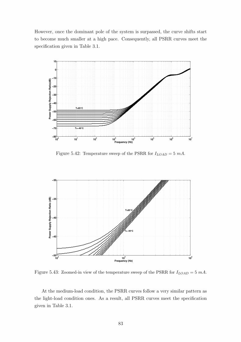
However, once the dominant pole of the system is surpassed, the curve shifts start
to become much smaller at a high pace. Consequently, all PSRR curves meet the
specification given in Table 3.1.
100
101
102
103
104
105
106
107
−80
−70
−60
−50
−40
−30
−20
−10
0
10
Po
wer
Su
pp
ly R
eje
cti
on
Rati
o(d
B)
Frequency (Hz)
T=85°C
T=−40°C
Figure 5.42: Temperature sweep of the PSRR for ILOAD = 5 mA.
103
104
105
−50
−45
−40
−35
−30
Po
wer
Su
pp
ly R
eje
cti
on
Rati
o (
dB
)
Frequency (Hz)
T=85°C
T=−40°C
Figure 5.43: Zoomed-in view of the temperature sweep of the PSRR for ILOAD = 5 mA.
At the medium-load condition, the PSRR curves follow a very similar pattern as
the light-load condition ones. As a result, all PSRR curves meet the specification
given in Table 3.1.
83
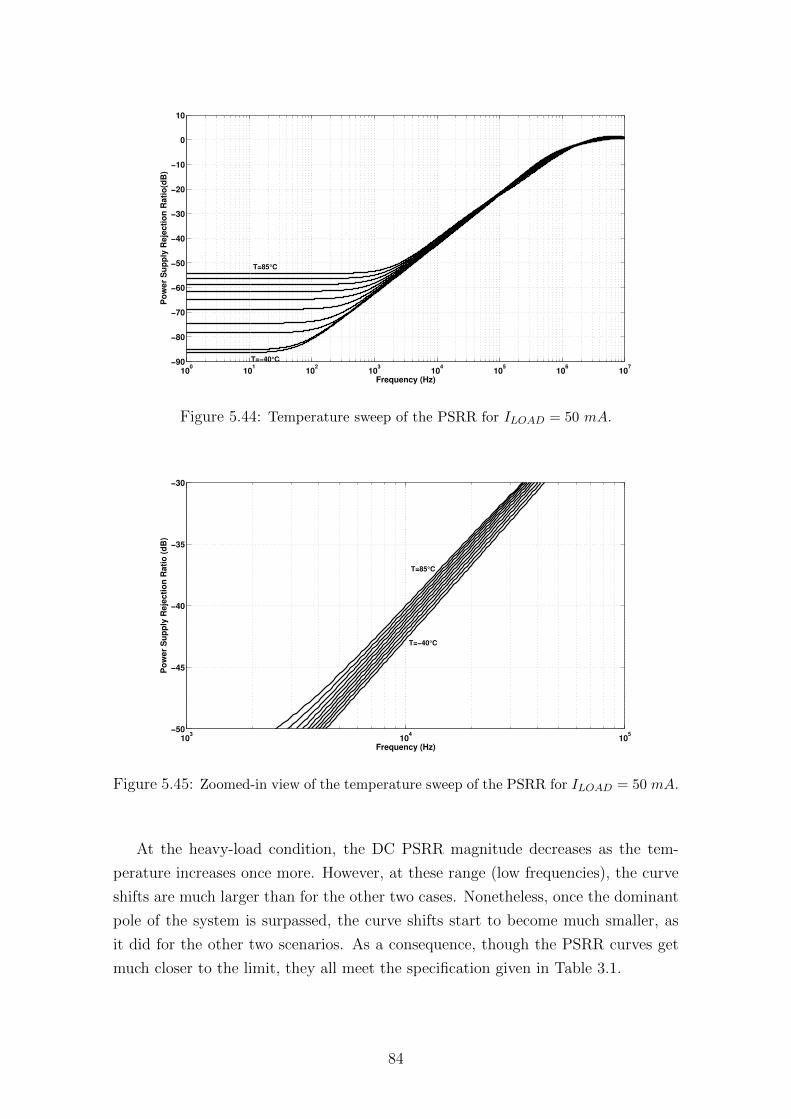
100
101
102
103
104
105
106
107
−90
−80
−70
−60
−50
−40
−30
−20
−10
0
10
Po
wer
Su
pp
ly R
eje
cti
on
Rati
o(d
B)
Frequency (Hz)
T=85°C
T=−40°C
Figure 5.44: Temperature sweep of the PSRR for ILOAD = 50 mA.
103
104
105
−50
−45
−40
−35
−30
Po
wer
Su
pp
ly R
eje
cti
on
Rati
o (
dB
)
Frequency (Hz)
T=85°C
T=−40°C
Figure 5.45: Zoomed-in view of the temperature sweep of the PSRR for ILOAD = 50 mA.
At the heavy-load condition, the DC PSRR magnitude decreases as the tem-
perature increases once more. However, at these range (low frequencies), the curve
shifts are much larger than for the other two cases. Nonetheless, once the dominant
pole of the system is surpassed, the curve shifts start to become much smaller, as
it did for the other two scenarios. As a consequence, though the PSRR curves get
much closer to the limit, they all meet the specification given in Table 3.1.
84
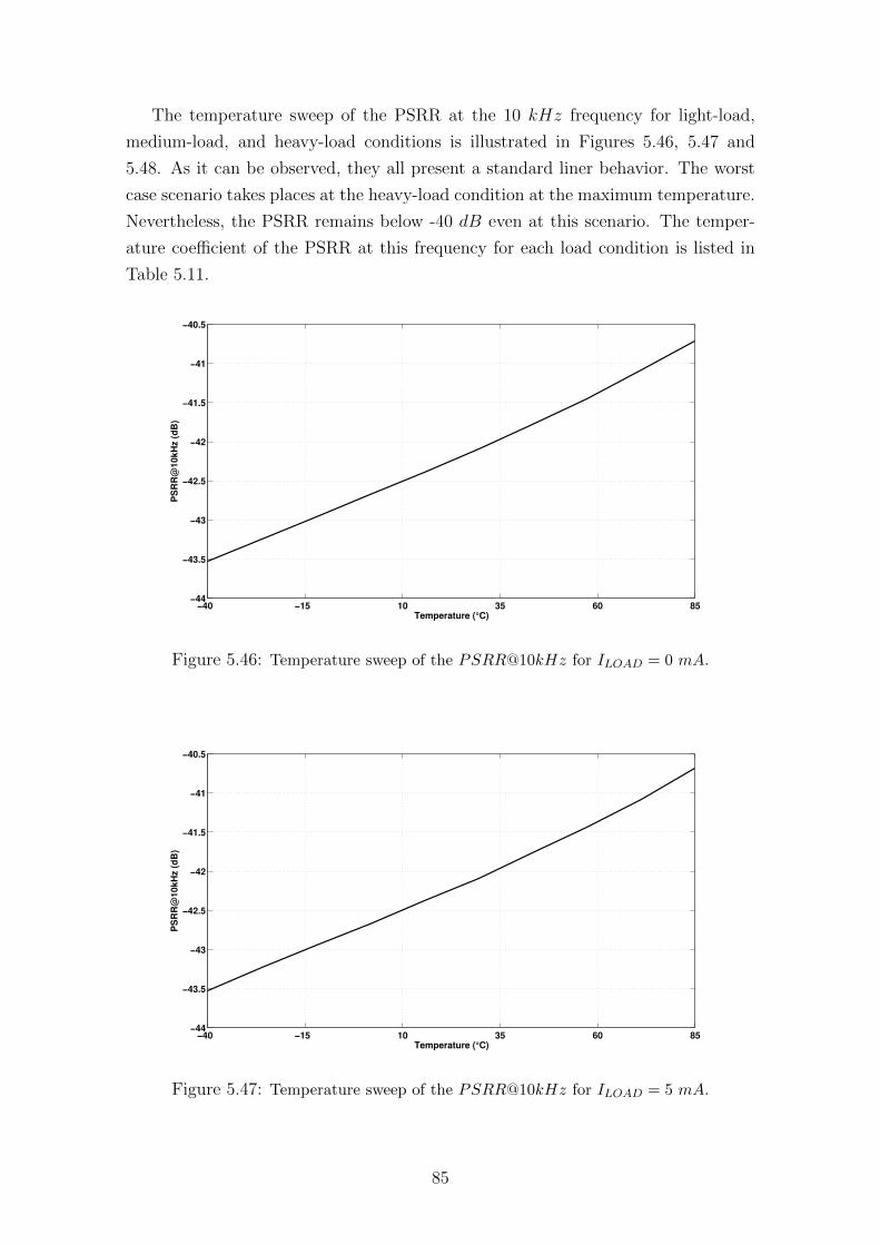
The temperature sweep of the PSRR at the 10 kHz frequency for light-load,
medium-load, and heavy-load conditions is illustrated in Figures 5.46, 5.47 and
5.48. As it can be observed, they all present a standard liner behavior. The worst
case scenario takes places at the heavy-load condition at the maximum temperature.
Nevertheless, the PSRR remains below -40 dB even at this scenario. The temper-
ature coefficient of the PSRR at this frequency for each load condition is listed in
Table 5.11.
−40 −15 10 35 60 85−44
−43.5
−43
−42.5
−42
−41.5
−41
−40.5
PS
RR
@10kH
z (
dB
)
Temperature (°C)
Figure 5.46: Temperature sweep of the PSRR@10kHz for ILOAD = 0 mA.
−40 −15 10 35 60 85−44
−43.5
−43
−42.5
−42
−41.5
−41
−40.5
PS
RR
@10kH
z (
dB
)
Temperature (°C)
Figure 5.47: Temperature sweep of the PSRR@10kHz for ILOAD = 5 mA.
85
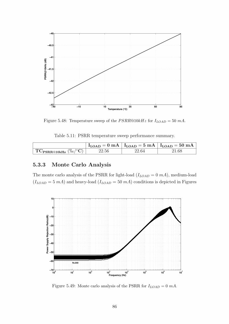
−40 −15 10 35 60 85−43
−42.5
−42
−41.5
−41
−40.5
−40
PS
RR
@10kH
z (
dB
)
Temperature (°C)
Figure 5.48: Temperature sweep of the PSRR@10kHz for ILOAD = 50 mA.
Table 5.11: PSRR temperature sweep performance summary.
ILOAD = 0 mA ILOAD = 5 mA ILOAD = 50 mATCPSRR@10kHz (h/C) 22.56 22.64 21.68
5.3.3 Monte Carlo Analysis
The monte carlo analysis of the PSRR for light-load (ILOAD = 0 mA), medium-load
(ILOAD = 5 mA) and heavy-load (ILOAD = 50 mA) conditions is depicted in Figures
100
101
102
103
104
105
106
107
−70
−60
−50
−40
−30
−20
−10
0
10
Po
wer
Su
pp
ly R
eje
cti
on
Rati
o(d
B)
Frequency (Hz)
N=200
Figure 5.49: Monte carlo analysis of the PSRR for ILOAD = 0 mA.
86
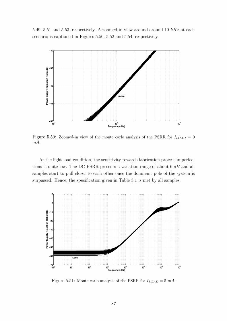
5.49, 5.51 and 5.53, respectively. A zoomed-in view around around 10 kHz at each
scenario is captioned in Figures 5.50, 5.52 and 5.54, respectively.
103
104
105
−50
−45
−40
−35
−30
Po
wer
Su
pp
ly R
eje
cti
on
Rati
o(d
B)
Frequency (Hz)
N=200
Figure 5.50: Zoomed-in view of the monte carlo analysis of the PSRR for ILOAD = 0mA.
At the light-load condition, the sensitivity towards fabrication process imperfec-
tions is quite low. The DC PSRR presents a variation range of about 6 dB and all
samples start to pull closer to each other once the dominant pole of the system is
surpassed. Hence, the specification given in Table 3.1 is met by all samples.
100
101
102
103
104
105
106
107
−70
−60
−50
−40
−30
−20
−10
0
10
Po
wer
Su
pp
ly R
eje
cti
on
Rati
o(d
B)
Frequency (Hz)
N=200
Figure 5.51: Monte carlo analysis of the PSRR for ILOAD = 5 mA.
87
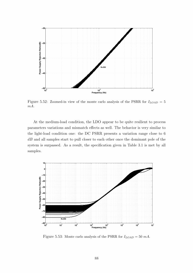
103
104
105
−50
−45
−40
−35
−30
Po
wer
Su
pp
ly R
eje
cti
on
Rati
o(d
B)
Frequency (Hz)
N=200
Figure 5.52: Zoomed-in view of the monte carlo analysis of the PSRR for ILOAD = 5mA.
At the medium-load condition, the LDO appear to be quite resilient to process
parameters variations and mismatch effects as well. The behavior is very similar to
the light-load condition one: the DC PSRR presents a variation range close to 6
dB and all samples start to pull closer to each other once the dominant pole of the
system is surpassed. As a result, the specification given in Table 3.1 is met by all
samples.
100
101
102
103
104
105
106
107
−90
−80
−70
−60
−50
−40
−30
−20
−10
0
10
Po
wer
Su
pp
ly R
eje
cti
on
Rati
o(d
B)
Frequency (Hz)
N=200
Figure 5.53: Monte carlo analysis of the PSRR for ILOAD = 50 mA.
88
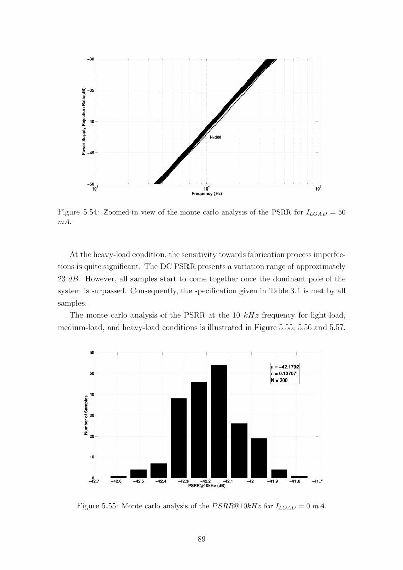
103
104
105
−50
−45
−40
−35
−30
Po
wer
Su
pp
ly R
eje
cti
on
Rati
o(d
B)
Frequency (Hz)
N=200
Figure 5.54: Zoomed-in view of the monte carlo analysis of the PSRR for ILOAD = 50mA.
At the heavy-load condition, the sensitivity towards fabrication process imperfec-
tions is quite significant. The DC PSRR presents a variation range of approximately
23 dB. However, all samples start to come together once the dominant pole of the
system is surpassed. Consequently, the specification given in Table 3.1 is met by all
samples.
The monte carlo analysis of the PSRR at the 10 kHz frequency for light-load,
medium-load, and heavy-load conditions is illustrated in Figure 5.55, 5.56 and 5.57.
−42.7 −42.6 −42.5 −42.4 −42.3 −42.2 −42.1 −42 −41.9 −41.8 −41.70
10
20
30
40
50
60
µ = −42.1792
σ = 0.13707
N = 200
Nu
mb
er
of
Sam
ple
s
PSRR@10kHz (dB)
Figure 5.55: Monte carlo analysis of the PSRR@10kHz for ILOAD = 0 mA.
89
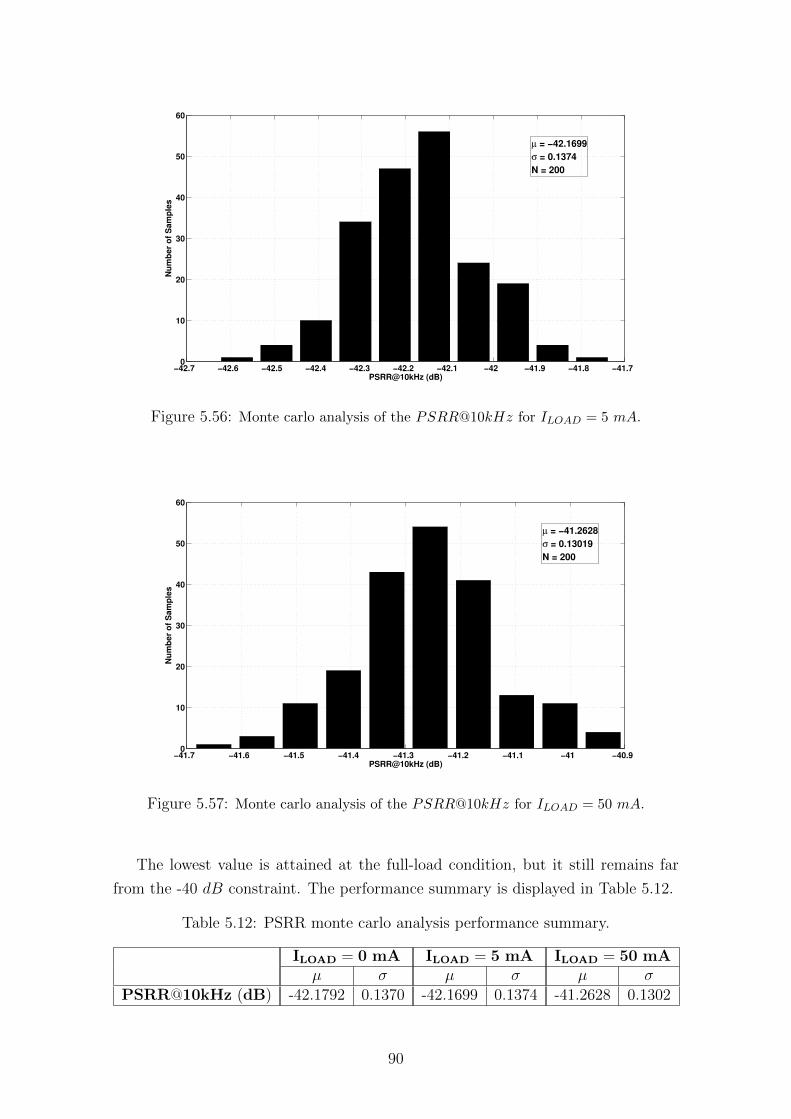
−42.7 −42.6 −42.5 −42.4 −42.3 −42.2 −42.1 −42 −41.9 −41.8 −41.70
10
20
30
40
50
60
µ = −42.1699
σ = 0.1374
N = 200N
um
ber
of
Sam
ple
s
PSRR@10kHz (dB)
Figure 5.56: Monte carlo analysis of the PSRR@10kHz for ILOAD = 5 mA.
−41.7 −41.6 −41.5 −41.4 −41.3 −41.2 −41.1 −41 −40.90
10
20
30
40
50
60
µ = −41.2628
σ = 0.13019
N = 200
Nu
mb
er
of
Sam
ple
s
PSRR@10kHz (dB)
Figure 5.57: Monte carlo analysis of the PSRR@10kHz for ILOAD = 50 mA.
The lowest value is attained at the full-load condition, but it still remains far
from the -40 dB constraint. The performance summary is displayed in Table 5.12.
Table 5.12: PSRR monte carlo analysis performance summary.
ILOAD = 0 mA ILOAD = 5 mA ILOAD = 50 mAµ σ µ σ µ σ
PSRR@10kHz (dB) -42.1792 0.1370 -42.1699 0.1374 -41.2628 0.1302
90
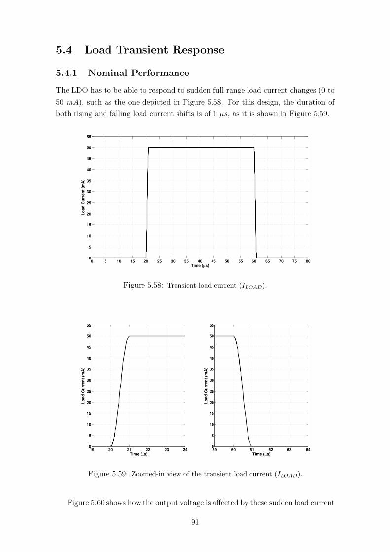
5.4 Load Transient Response
5.4.1 Nominal Performance
The LDO has to be able to respond to sudden full range load current changes (0 to
50 mA), such as the one depicted in Figure 5.58. For this design, the duration of
both rising and falling load current shifts is of 1 µs, as it is shown in Figure 5.59.
0 5 10 15 20 25 30 35 40 45 50 55 60 65 70 75 800
5
10
15
20
25
30
35
40
45
50
55
Lo
ad
Cu
rren
t (m
A)
Time (µs)
Figure 5.58: Transient load current (ILOAD).
19 20 21 22 23 240
5
10
15
20
25
30
35
40
45
50
55
Lo
ad
Cu
rren
t (m
A)
Time (µs)59 60 61 62 63 640
5
10
15
20
25
30
35
40
45
50
55
Lo
ad
Cu
rren
t (m
A)
Time (µs)
Figure 5.59: Zoomed-in view of the transient load current (ILOAD).
Figure 5.60 shows how the output voltage is affected by these sudden load current
91
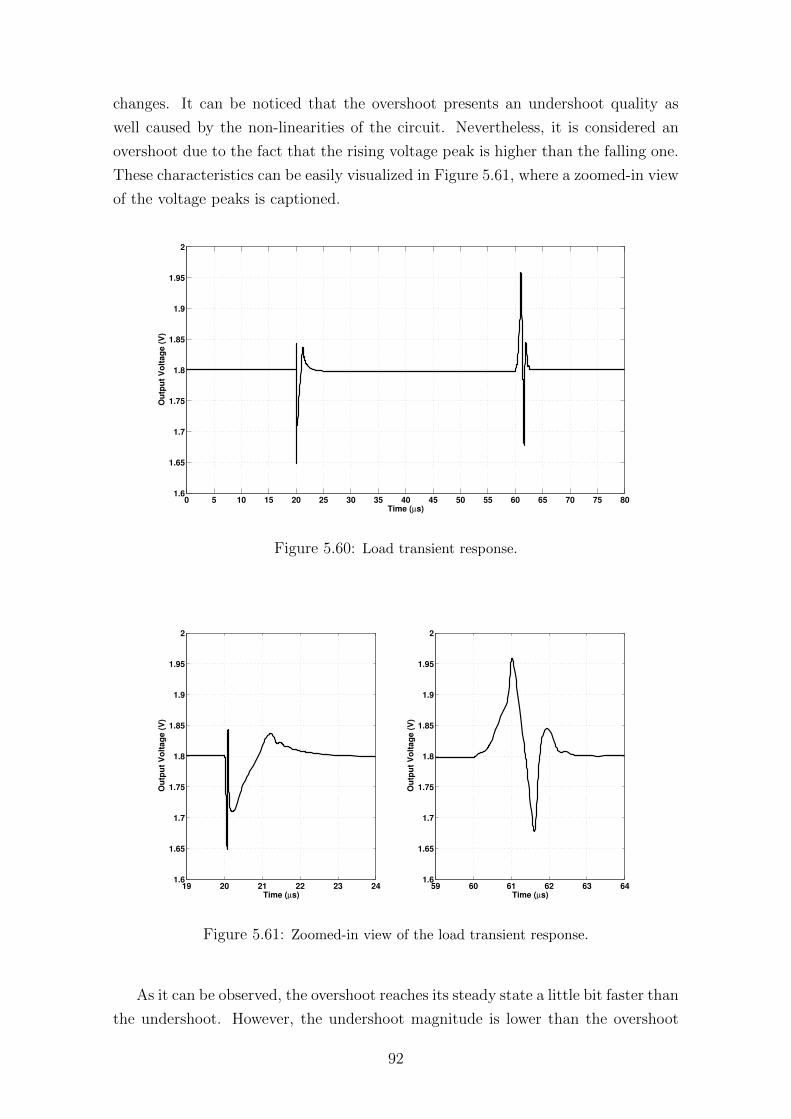
changes. It can be noticed that the overshoot presents an undershoot quality as
well caused by the non-linearities of the circuit. Nevertheless, it is considered an
overshoot due to the fact that the rising voltage peak is higher than the falling one.
These characteristics can be easily visualized in Figure 5.61, where a zoomed-in view
of the voltage peaks is captioned.
0 5 10 15 20 25 30 35 40 45 50 55 60 65 70 75 801.6
1.65
1.7
1.75
1.8
1.85
1.9
1.95
2
Ou
tpu
t V
olt
ag
e (
V)
Time (µs)
Figure 5.60: Load transient response.
19 20 21 22 23 241.6
1.65
1.7
1.75
1.8
1.85
1.9
1.95
2
Ou
tpu
t V
olt
ag
e (
V)
Time (µs)59 60 61 62 63 64
1.6
1.65
1.7
1.75
1.8
1.85
1.9
1.95
2
Ou
tpu
t V
olt
ag
e (
V)
Time (µs)
Figure 5.61: Zoomed-in view of the load transient response.
As it can be observed, the overshoot reaches its steady state a little bit faster than
the undershoot. However, the undershoot magnitude is lower than the overshoot
92
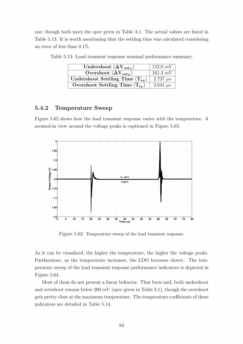
one; though both meet the spec given in Table 3.1. The actual values are listed in
Table 5.13. It is worth mentioning that the settling time was calculated considering
an error of less than 0.1%.
Table 5.13: Load transient response nominal performance summary.
Undershoot (∆VoutN) 152.0 mVOvershoot (∆VoutP) 161.3 mV
Undershoot Settling Time (TsN) 2.737 µsOvershoot Settling Time (TsP) 2.641 µs
5.4.2 Temperature Sweep
Figure 5.62 shows how the load transient response varies with the temperature. A
zoomed-in view around the voltage peaks is captioned in Figure 5.63.
0 5 10 15 20 25 30 35 40 45 50 55 60 65 70 75 801.6
1.65
1.7
1.75
1.8
1.85
1.9
1.95
2
Ou
tpu
t V
olt
ag
e (
V)
Time (µs)
T=−40°C
T=85°C
Figure 5.62: Temperature sweep of the load transient response.
As it can be visualized, the higher the temperature, the higher the voltage peaks.
Furthermore, as the temperature increases, the LDO becomes slower. The tem-
perature sweep of the load transient response performance indicators is depicted in
Figure 5.64.
Most of them do not present a linear behavior. That been said, both undershoot
and overshoot remain below 200 mV (spec given in Table 3.1), though the overshoot
gets pretty close at the maximum temperature. The temperature coefficients of these
indicators are detailed in Table 5.14.
93
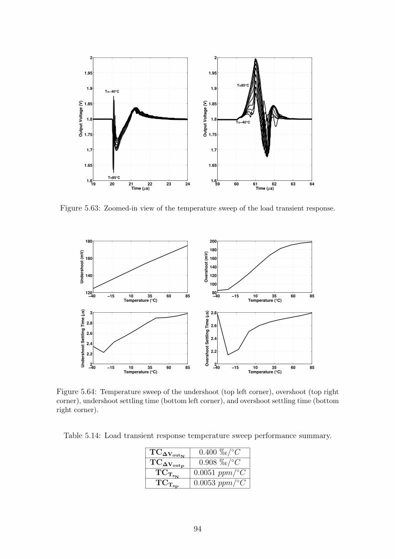
19 20 21 22 23 241.6
1.65
1.7
1.75
1.8
1.85
1.9
1.95
2
Ou
tpu
t V
olt
ag
e (
V)
Time (µs)
T=−40°C
T=85°C
59 60 61 62 63 641.6
1.65
1.7
1.75
1.8
1.85
1.9
1.95
2
Ou
tpu
t V
olt
ag
e (
V)
Time (µs)
T=85°C
T=−40°C
Figure 5.63: Zoomed-in view of the temperature sweep of the load transient response.
−40 −15 10 35 60 85120
140
160
180
Un
ders
ho
ot
(mV
)
Temperature (°C)−40 −15 10 35 60 8580
100
120
140
160
180
200
Overs
ho
ot
(mV
)
Temperature (°C)
−40 −15 10 35 60 852
2.2
2.4
2.6
2.8
3
Un
ders
ho
ot
Sett
lin
g T
ime (µ
s)
Temperature (°C)−40 −15 10 35 60 852
2.2
2.4
2.6
2.8
Overs
ho
ot
Sett
lin
g T
ime (µ
s)
Temperature (°C)
Figure 5.64: Temperature sweep of the undershoot (top left corner), overshoot (top rightcorner), undershoot settling time (bottom left corner), and overshoot settling time (bottomright corner).
Table 5.14: Load transient response temperature sweep performance summary.
TC∆VoutN0.400 h/C
TC∆VoutP0.908 h/C
TCTsN0.0051 ppm/C
TCTsP0.0053 ppm/C
94
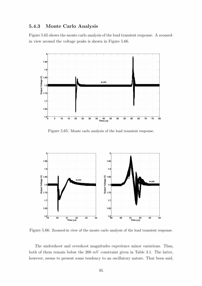
5.4.3 Monte Carlo Analysis
Figure 5.65 shows the monte carlo analysis of the load transient response. A zoomed-
in view around the voltage peaks is shown in Figure 5.66.
0 5 10 15 20 25 30 35 40 45 50 55 60 65 70 75 801.6
1.65
1.7
1.75
1.8
1.85
1.9
1.95
2
Ou
tpu
t V
olt
ag
e (
V)
Time (µs)
N=200
Figure 5.65: Monte carlo analysis of the load transient response.
19 20 21 22 23 241.6
1.65
1.7
1.75
1.8
1.85
1.9
1.95
2
Ou
tpu
t V
olt
ag
e (
V)
Time (µs)
N=200
59 60 61 62 63 641.6
1.65
1.7
1.75
1.8
1.85
1.9
1.95
2
Ou
tpu
t V
olt
ag
e (
V)
Time (µs)
N=200
Figure 5.66: Zoomed-in view of the monte carlo analysis of the load transient response.
The undershoot and overshoot magnitudes experience minor variations. Thus,
both of them remain below the 200 mV constraint given in Table 3.1. The latter,
however, seems to present some tendency to an oscillatory nature. That been said,
95
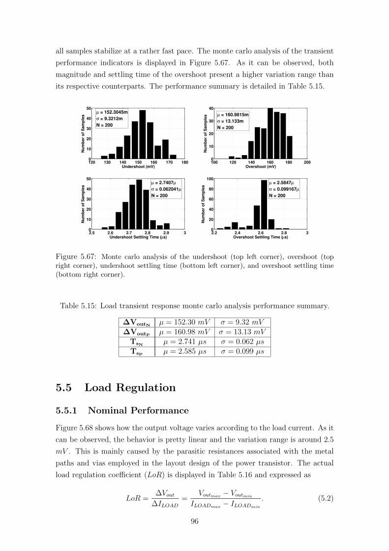
all samples stabilize at a rather fast pace. The monte carlo analysis of the transient
performance indicators is displayed in Figure 5.67. As it can be observed, both
magnitude and settling time of the overshoot present a higher variation range than
its respective counterparts. The performance summary is detailed in Table 5.15.
120 130 140 150 160 170 1800
10
20
30
40
50µ = 152.3045m
σ = 9.3212m
N = 200
Nu
mb
er
of
Sam
ple
s
Undershoot (mV)100 120 140 160 180 2000
10
20
30
40
µ = 160.9815m
σ = 13.133m
N = 200
Nu
mb
er
of
Sam
ple
s
Overshoot (mV)
2.5 2.6 2.7 2.8 2.9 30
10
20
30
40
50µ = 2.7407µ
σ = 0.062041µ
N = 200
Nu
mb
er
of
Sam
ple
s
Undershoot Settling Time (µs)2.2 2.4 2.6 2.8 30
20
40
60
80
100µ = 2.5847µ
σ = 0.099167µ
N = 200
Nu
mb
er
of
Sam
ple
s
Overshoot Settling Time (µs)
Figure 5.67: Monte carlo analysis of the undershoot (top left corner), overshoot (topright corner), undershoot settling time (bottom left corner), and overshoot settling time(bottom right corner).
Table 5.15: Load transient response monte carlo analysis performance summary.
∆VoutN µ = 152.30 mV σ = 9.32 mV∆VoutP µ = 160.98 mV σ = 13.13 mV
TsN µ = 2.741 µs σ = 0.062 µsTsP µ = 2.585 µs σ = 0.099 µs
5.5 Load Regulation
5.5.1 Nominal Performance
Figure 5.68 shows how the output voltage varies according to the load current. As it
can be observed, the behavior is pretty linear and the variation range is around 2.5
mV . This is mainly caused by the parasitic resistances associated with the metal
paths and vias employed in the layout design of the power transistor. The actual
load regulation coefficient (LoR) is displayed in Table 5.16 and expressed as
LoR =∆Vout
∆ILOAD=
Voutmax − Voutmin
ILOADmax − ILOADmin
. (5.2)
96
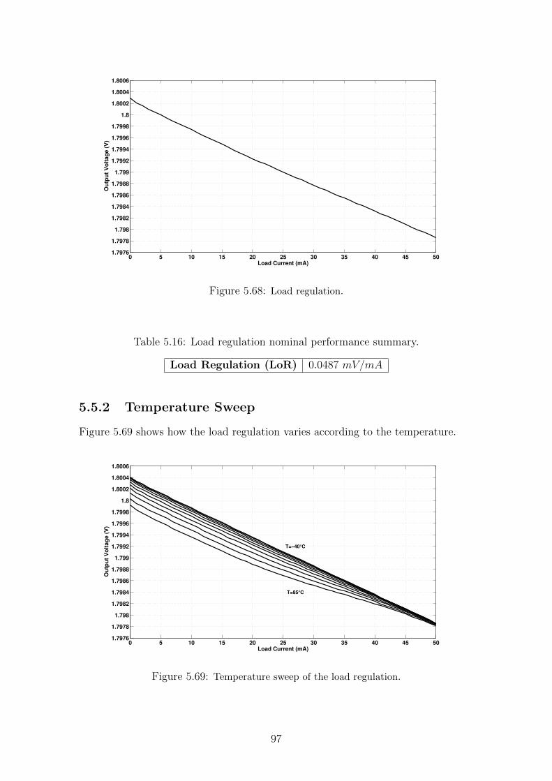
0 5 10 15 20 25 30 35 40 45 501.7976
1.7978
1.798
1.7982
1.7984
1.7986
1.7988
1.799
1.7992
1.7994
1.7996
1.7998
1.8
1.8002
1.8004
1.8006
Ou
tpu
t V
olt
ag
e (
V)
Load Current (mA)
Figure 5.68: Load regulation.
Table 5.16: Load regulation nominal performance summary.
Load Regulation (LoR) 0.0487 mV/mA
5.5.2 Temperature Sweep
Figure 5.69 shows how the load regulation varies according to the temperature.
0 5 10 15 20 25 30 35 40 45 501.7976
1.7978
1.798
1.7982
1.7984
1.7986
1.7988
1.799
1.7992
1.7994
1.7996
1.7998
1.8
1.8002
1.8004
1.8006
Ou
tpu
t V
olt
ag
e (
V)
Load Current (mA)
T=−40°C
T=85°C
Figure 5.69: Temperature sweep of the load regulation.
97
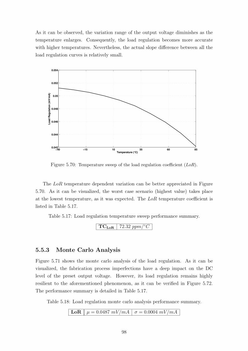
As it can be observed, the variation range of the output voltage diminishes as the
temperature enlarges. Consequently, the load regulation becomes more accurate
with higher temperatures. Nevertheless, the actual slope difference between all the
load regulation curves is relatively small.
−40 −15 10 35 60 850.042
0.044
0.046
0.048
0.05
0.052
0.054
Lo
ad
Reg
ula
tio
n (
mV
/mA
)
Temperature (°C)
Figure 5.70: Temperature sweep of the load regulation coefficient (LoR).
The LoR temperature dependent variation can be better appreciated in Figure
5.70. As it can be visualized, the worst case scenario (highest value) takes place
at the lowest temperature, as it was expected. The LoR temperature coefficient is
listed in Table 5.17.
Table 5.17: Load regulation temperature sweep performance summary.
TCLoR 72.32 ppm/C
5.5.3 Monte Carlo Analysis
Figure 5.71 shows the monte carlo analysis of the load regulation. As it can be
visualized, the fabrication process imperfections have a deep impact on the DC
level of the preset output voltage. However, its load regulation remains highly
resilient to the aforementioned phenomenon, as it can be verified in Figure 5.72.
The performance summary is detailed in Table 5.17.
Table 5.18: Load regulation monte carlo analysis performance summary.
LoR µ = 0.0487 mV/mA σ = 0.0004 mV/mA
98
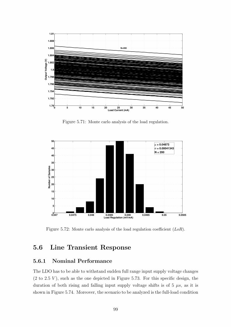
0 5 10 15 20 25 30 35 40 45 501.79
1.792
1.794
1.796
1.798
1.8
1.802
1.804
1.806
1.808
1.81
Ou
tpu
t V
olt
ag
e (
V)
Load Current (mA)
N=200
Figure 5.71: Monte carlo analysis of the load regulation.
0.047 0.0475 0.048 0.0485 0.049 0.0495 0.05 0.05050
5
10
15
20
25
30
35
40
45
50
µ = 0.04873
σ = 0.00041343
N = 200
Nu
mb
er
of
Sam
ple
s
Load Regulation (mV/mA)
Figure 5.72: Monte carlo analysis of the load regulation coefficient (LoR).
5.6 Line Transient Response
5.6.1 Nominal Performance
The LDO has to be able to withstand sudden full range input supply voltage changes
(2 to 2.5 V ), such as the one depicted in Figure 5.73. For this specific design, the
duration of both rising and falling input supply voltage shifts is of 5 µs, as it is
shown in Figure 5.74. Moreover, the scenario to be analyzed is the full-load condition
99
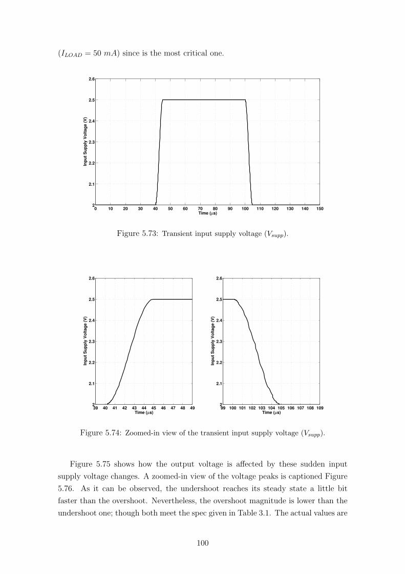
(ILOAD = 50 mA) since is the most critical one.
0 10 20 30 40 50 60 70 80 90 100 110 120 130 140 1502
2.1
2.2
2.3
2.4
2.5
2.6
Inp
ut
Su
pp
ly V
olt
ag
e (
V)
Time (µs)
Figure 5.73: Transient input supply voltage (Vsupp).
39 40 41 42 43 44 45 46 47 48 492
2.1
2.2
2.3
2.4
2.5
2.6
Inp
ut
Su
pp
ly V
olt
ag
e (
V)
Time (µs)99 100 101 102 103 104 105 106 107 108 1092
2.1
2.2
2.3
2.4
2.5
2.6
Inp
ut
Su
pp
ly V
olt
ag
e (
V)
Time (µs)
Figure 5.74: Zoomed-in view of the transient input supply voltage (Vsupp).
Figure 5.75 shows how the output voltage is affected by these sudden input
supply voltage changes. A zoomed-in view of the voltage peaks is captioned Figure
5.76. As it can be observed, the undershoot reaches its steady state a little bit
faster than the overshoot. Nevertheless, the overshoot magnitude is lower than the
undershoot one; though both meet the spec given in Table 3.1. The actual values are
100
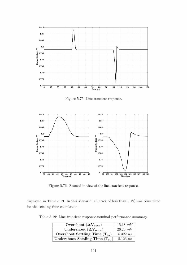
0 10 20 30 40 50 60 70 80 90 100 110 120 130 140 1501.77
1.775
1.78
1.785
1.79
1.795
1.8
1.805
1.81
1.815
Ou
tpu
t V
olt
ag
e (
V)
Time (µs)
Figure 5.75: Line transient response.
39 40 41 42 43 44 45 46 47 48 491.77
1.775
1.78
1.785
1.79
1.795
1.8
1.805
1.81
1.815
Ou
tpu
t V
olt
ag
e (
V)
Time (µs)99 100 101 102 103 104 105 106 107 108 109
1.77
1.775
1.78
1.785
1.79
1.795
1.8
1.805
1.81
1.815
Ou
tpu
t V
olt
ag
e (
V)
Time (µs)
Figure 5.76: Zoomed-in view of the line transient response.
displayed in Table 5.19. In this scenario, an error of less than 0.1% was considered
for the settling time calculation.
Table 5.19: Line transient response nominal performance summary.
Overshoot (∆VoutP) 15.18 mVUndershoot (∆VoutN) 26.20 mV
Overshoot Settling Time (TsP) 5.322 µsUndershoot Settling Time (TsN) 5.126 µs
101
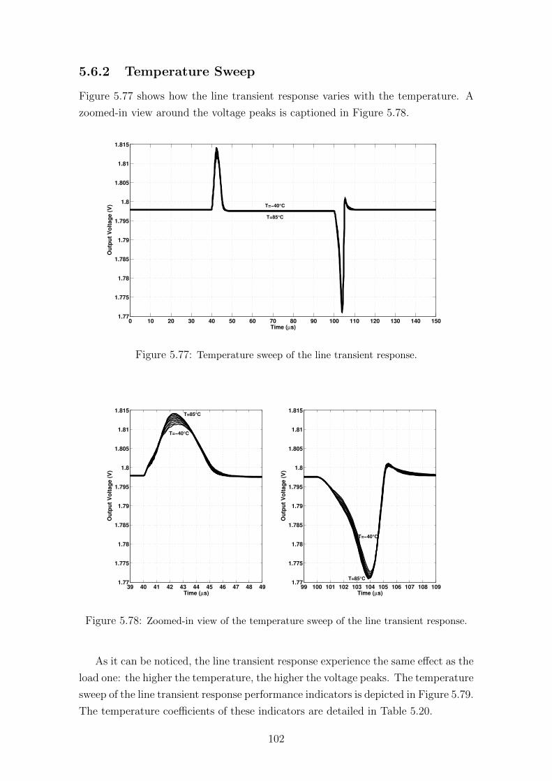
5.6.2 Temperature Sweep
Figure 5.77 shows how the line transient response varies with the temperature. A
zoomed-in view around the voltage peaks is captioned in Figure 5.78.
0 10 20 30 40 50 60 70 80 90 100 110 120 130 140 1501.77
1.775
1.78
1.785
1.79
1.795
1.8
1.805
1.81
1.815
Ou
tpu
t V
olt
ag
e (
V)
Time (µs)
T=−40°C
T=85°C
Figure 5.77: Temperature sweep of the line transient response.
39 40 41 42 43 44 45 46 47 48 491.77
1.775
1.78
1.785
1.79
1.795
1.8
1.805
1.81
1.815
Ou
tpu
t V
olt
ag
e (
V)
Time (µs)
T=85°C
T=−40°C
99 100 101 102 103 104 105 106 107 108 1091.77
1.775
1.78
1.785
1.79
1.795
1.8
1.805
1.81
1.815
Ou
tpu
t V
olt
ag
e (
V)
Time (µs)
T=−40°C
T=85°C
Figure 5.78: Zoomed-in view of the temperature sweep of the line transient response.
As it can be noticed, the line transient response experience the same effect as the
load one: the higher the temperature, the higher the voltage peaks. The temperature
sweep of the line transient response performance indicators is depicted in Figure 5.79.
The temperature coefficients of these indicators are detailed in Table 5.20.
102
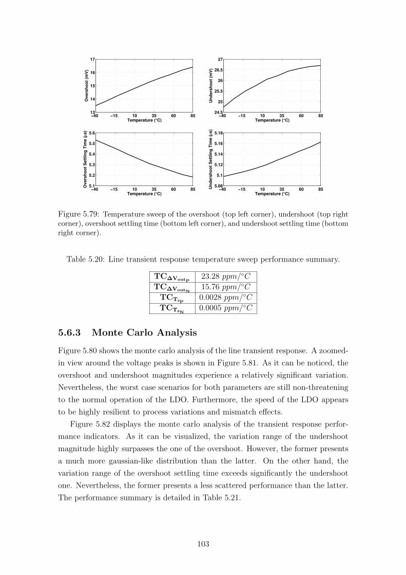
−40 −15 10 35 60 8513
14
15
16
17
Overs
ho
ot
(mV
)
Temperature (°C)−40 −15 10 35 60 85
24.5
25
25.5
26
26.5
27
Un
ders
ho
ot
(mV
)
Temperature (°C)
−40 −15 10 35 60 855.1
5.2
5.3
5.4
5.5
5.6
Overs
ho
ot
Sett
lin
g T
ime (µ
s)
Temperature (°C)−40 −15 10 35 60 85
5.08
5.1
5.12
5.14
5.16
5.18
Un
ders
ho
ot
Sett
lin
g T
ime (µ
s)
Temperature (°C)
Figure 5.79: Temperature sweep of the overshoot (top left corner), undershoot (top rightcorner), overshoot settling time (bottom left corner), and undershoot settling time (bottomright corner).
Table 5.20: Line transient response temperature sweep performance summary.
TC∆VoutP23.28 ppm/C
TC∆VoutN15.76 ppm/C
TCTsP0.0028 ppm/C
TCTsN0.0005 ppm/C
5.6.3 Monte Carlo Analysis
Figure 5.80 shows the monte carlo analysis of the line transient response. A zoomed-
in view around the voltage peaks is shown in Figure 5.81. As it can be noticed, the
overshoot and undershoot magnitudes experience a relatively significant variation.
Nevertheless, the worst case scenarios for both parameters are still non-threatening
to the normal operation of the LDO. Furthermore, the speed of the LDO appears
to be highly resilient to process variations and mismatch effects.
Figure 5.82 displays the monte carlo analysis of the transient response perfor-
mance indicators. As it can be visualized, the variation range of the undershoot
magnitude highly surpasses the one of the overshoot. However, the former presents
a much more gaussian-like distribution than the latter. On the other hand, the
variation range of the overshoot settling time exceeds significantly the undershoot
one. Nevertheless, the former presents a less scattered performance than the latter.
The performance summary is detailed in Table 5.21.
103
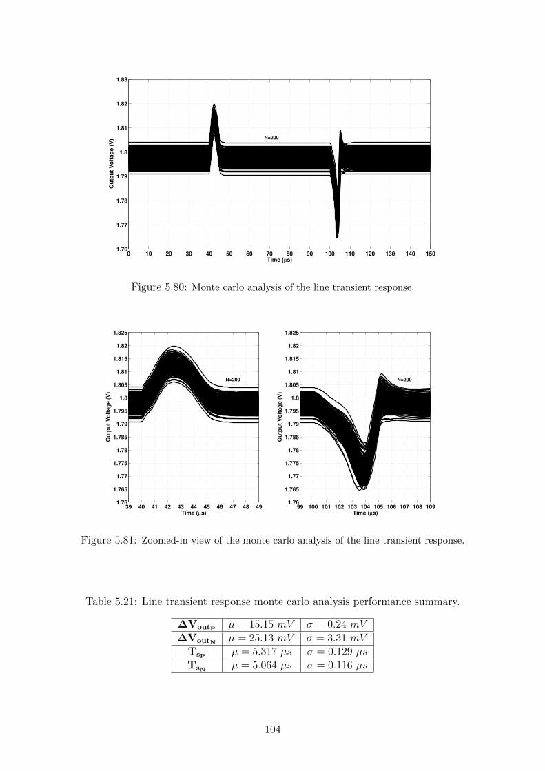
0 10 20 30 40 50 60 70 80 90 100 110 120 130 140 1501.76
1.77
1.78
1.79
1.8
1.81
1.82
1.83
Ou
tpu
t V
olt
ag
e (
V)
Time (µs)
N=200
Figure 5.80: Monte carlo analysis of the line transient response.
39 40 41 42 43 44 45 46 47 48 491.76
1.765
1.77
1.775
1.78
1.785
1.79
1.795
1.8
1.805
1.81
1.815
1.82
1.825
Ou
tpu
t V
olt
ag
e (
V)
Time (µs)
N=200
99 100 101 102 103 104 105 106 107 108 1091.76
1.765
1.77
1.775
1.78
1.785
1.79
1.795
1.8
1.805
1.81
1.815
1.82
1.825
Ou
tpu
t V
olt
ag
e (
V)
Time (µs)
N=200
Figure 5.81: Zoomed-in view of the monte carlo analysis of the line transient response.
Table 5.21: Line transient response monte carlo analysis performance summary.
∆VoutP µ = 15.15 mV σ = 0.24 mV∆VoutN µ = 25.13 mV σ = 3.31 mV
TsP µ = 5.317 µs σ = 0.129 µsTsN µ = 5.064 µs σ = 0.116 µs
104
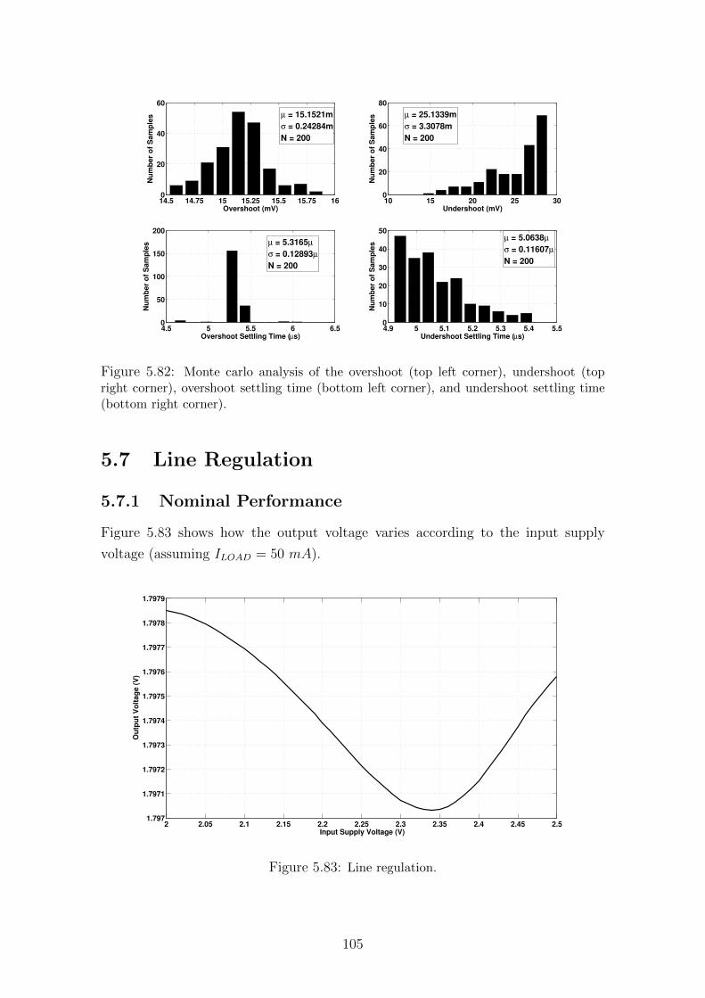
14.5 14.75 15 15.25 15.5 15.75 160
20
40
60
µ = 15.1521m
σ = 0.24284m
N = 200
Nu
mb
er
of
Sam
ple
s
Overshoot (mV)10 15 20 25 300
20
40
60
80
µ = 25.1339m
σ = 3.3078m
N = 200
Nu
mb
er
of
Sam
ple
s
Undershoot (mV)
4.5 5 5.5 6 6.50
50
100
150
200
µ = 5.3165µ
σ = 0.12893µ
N = 200
Nu
mb
er
of
Sam
ple
s
Overshoot Settling Time (µs)4.9 5 5.1 5.2 5.3 5.4 5.50
10
20
30
40
50µ = 5.0638µ
σ = 0.11607µ
N = 200
Nu
mb
er
of
Sam
ple
s
Undershoot Settling Time (µs)
Figure 5.82: Monte carlo analysis of the overshoot (top left corner), undershoot (topright corner), overshoot settling time (bottom left corner), and undershoot settling time(bottom right corner).
5.7 Line Regulation
5.7.1 Nominal Performance
Figure 5.83 shows how the output voltage varies according to the input supply
voltage (assuming ILOAD = 50 mA).
2 2.05 2.1 2.15 2.2 2.25 2.3 2.35 2.4 2.45 2.51.797
1.7971
1.7972
1.7973
1.7974
1.7975
1.7976
1.7977
1.7978
1.7979
Ou
tpu
t V
olt
ag
e (
V)
Input Supply Voltage (V)
Figure 5.83: Line regulation.
105
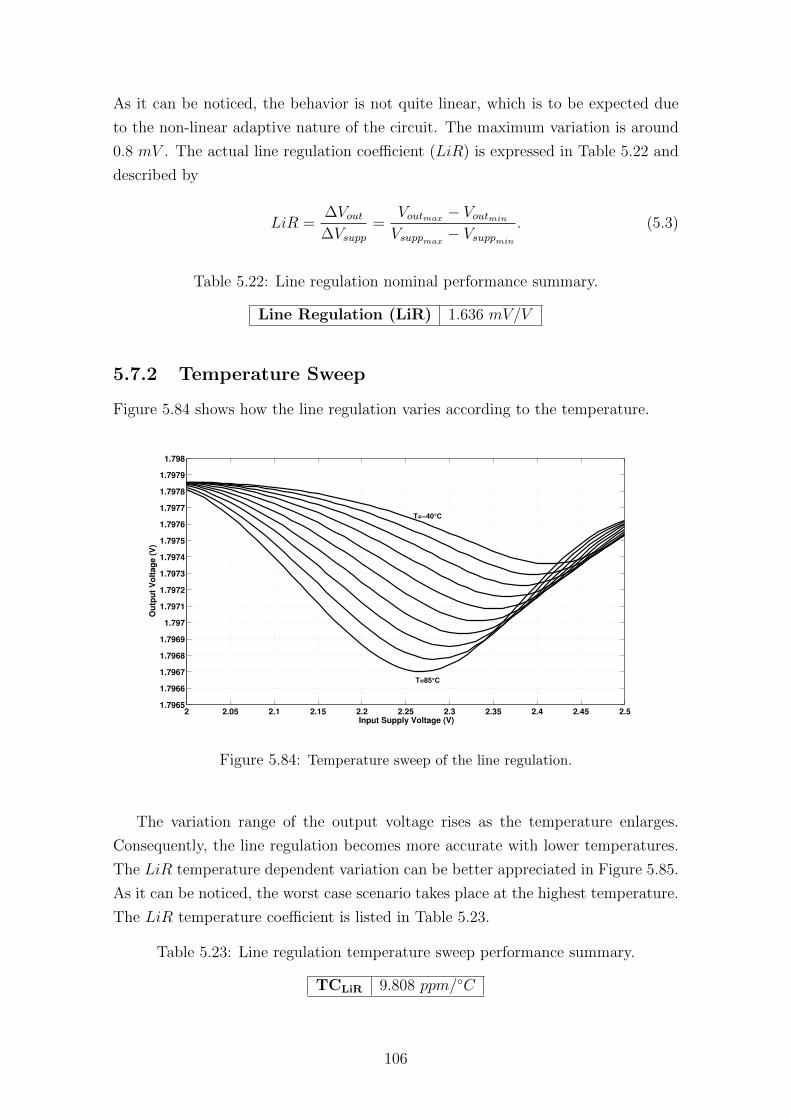
As it can be noticed, the behavior is not quite linear, which is to be expected due
to the non-linear adaptive nature of the circuit. The maximum variation is around
0.8 mV . The actual line regulation coefficient (LiR) is expressed in Table 5.22 and
described by
LiR =∆Vout∆Vsupp
=Voutmax − Voutmin
Vsuppmax− Vsuppmin
. (5.3)
Table 5.22: Line regulation nominal performance summary.
Line Regulation (LiR) 1.636 mV/V
5.7.2 Temperature Sweep
Figure 5.84 shows how the line regulation varies according to the temperature.
2 2.05 2.1 2.15 2.2 2.25 2.3 2.35 2.4 2.45 2.51.7965
1.7966
1.7967
1.7968
1.7969
1.797
1.7971
1.7972
1.7973
1.7974
1.7975
1.7976
1.7977
1.7978
1.7979
1.798
Ou
tpu
t V
olt
ag
e (
V)
Input Supply Voltage (V)
T=−40°C
T=85°C
Figure 5.84: Temperature sweep of the line regulation.
The variation range of the output voltage rises as the temperature enlarges.
Consequently, the line regulation becomes more accurate with lower temperatures.
The LiR temperature dependent variation can be better appreciated in Figure 5.85.
As it can be noticed, the worst case scenario takes place at the highest temperature.
The LiR temperature coefficient is listed in Table 5.23.
Table 5.23: Line regulation temperature sweep performance summary.
TCLiR 9.808 ppm/C
106
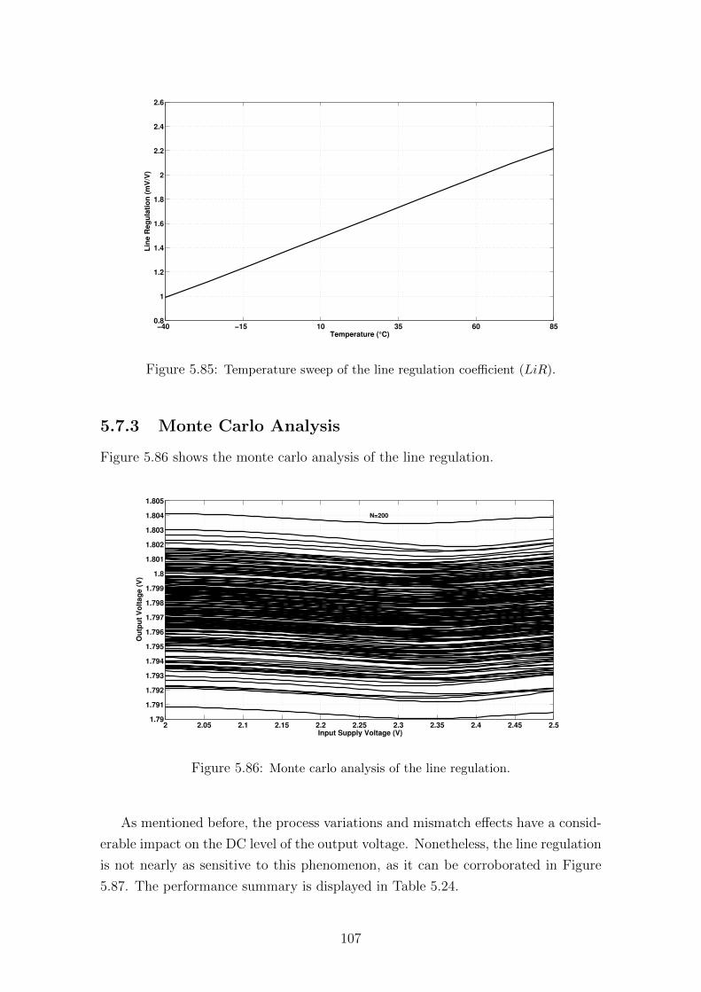
−40 −15 10 35 60 850.8
1
1.2
1.4
1.6
1.8
2
2.2
2.4
2.6
Lin
e R
eg
ula
tio
n (
mV
/V)
Temperature (°C)
Figure 5.85: Temperature sweep of the line regulation coefficient (LiR).
5.7.3 Monte Carlo Analysis
Figure 5.86 shows the monte carlo analysis of the line regulation.
2 2.05 2.1 2.15 2.2 2.25 2.3 2.35 2.4 2.45 2.51.79
1.791
1.792
1.793
1.794
1.795
1.796
1.797
1.798
1.799
1.8
1.801
1.802
1.803
1.804
1.805
Ou
tpu
t V
olt
ag
e (
V)
Input Supply Voltage (V)
N=200
Figure 5.86: Monte carlo analysis of the line regulation.
As mentioned before, the process variations and mismatch effects have a consid-
erable impact on the DC level of the output voltage. Nonetheless, the line regulation
is not nearly as sensitive to this phenomenon, as it can be corroborated in Figure
5.87. The performance summary is displayed in Table 5.24.
107
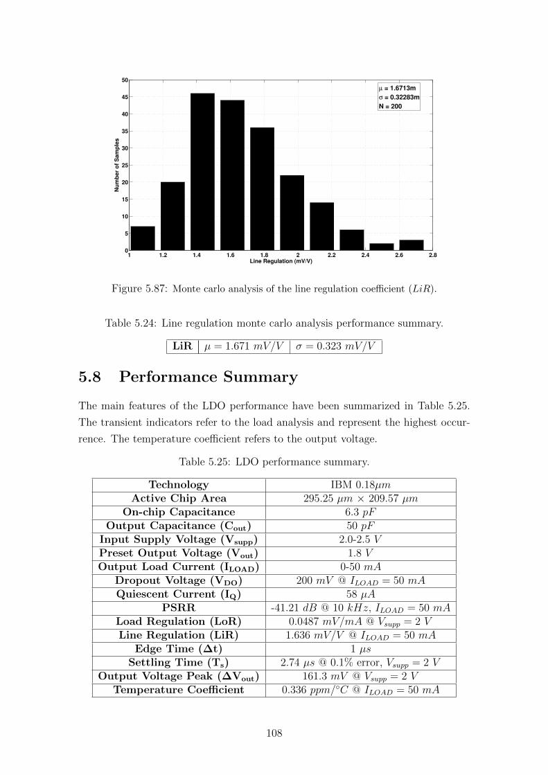
1 1.2 1.4 1.6 1.8 2 2.2 2.4 2.6 2.80
5
10
15
20
25
30
35
40
45
50
µ = 1.6713m
σ = 0.32283m
N = 200
Nu
mb
er
of
Sam
ple
s
Line Regulation (mV/V)
Figure 5.87: Monte carlo analysis of the line regulation coefficient (LiR).
Table 5.24: Line regulation monte carlo analysis performance summary.
LiR µ = 1.671 mV/V σ = 0.323 mV/V
5.8 Performance Summary
The main features of the LDO performance have been summarized in Table 5.25.
The transient indicators refer to the load analysis and represent the highest occur-
rence. The temperature coefficient refers to the output voltage.
Table 5.25: LDO performance summary.
Technology IBM 0.18µmActive Chip Area 295.25 µm × 209.57 µm
On-chip Capacitance 6.3 pFOutput Capacitance (Cout) 50 pF
Input Supply Voltage (Vsupp) 2.0-2.5 VPreset Output Voltage (Vout) 1.8 VOutput Load Current (ILOAD) 0-50 mA
Dropout Voltage (VDO) 200 mV @ ILOAD = 50 mAQuiescent Current (IQ) 58 µA
PSRR -41.21 dB @ 10 kHz, ILOAD = 50 mALoad Regulation (LoR) 0.0487 mV/mA @ Vsupp = 2 VLine Regulation (LiR) 1.636 mV/V @ ILOAD = 50 mA
Edge Time (∆t) 1 µsSettling Time (Ts) 2.74 µs @ 0.1% error, Vsupp = 2 V
Output Voltage Peak (∆Vout) 161.3 mV @ Vsupp = 2 VTemperature Coefficient 0.336 ppm/C @ ILOAD = 50 mA
108
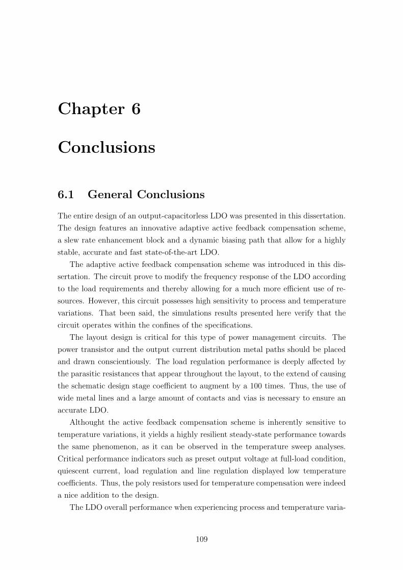
Chapter 6
Conclusions
6.1 General Conclusions
The entire design of an output-capacitorless LDO was presented in this dissertation.
The design features an innovative adaptive active feedback compensation scheme,
a slew rate enhancement block and a dynamic biasing path that allow for a highly
stable, accurate and fast state-of-the-art LDO.
The adaptive active feedback compensation scheme was introduced in this dis-
sertation. The circuit prove to modify the frequency response of the LDO according
to the load requirements and thereby allowing for a much more efficient use of re-
sources. However, this circuit possesses high sensitivity to process and temperature
variations. That been said, the simulations results presented here verify that the
circuit operates within the confines of the specifications.
The layout design is critical for this type of power management circuits. The
power transistor and the output current distribution metal paths should be placed
and drawn conscientiously. The load regulation performance is deeply affected by
the parasitic resistances that appear throughout the layout, to the extend of causing
the schematic design stage coefficient to augment by a 100 times. Thus, the use of
wide metal lines and a large amount of contacts and vias is necessary to ensure an
accurate LDO.
Althought the active feedback compensation scheme is inherently sensitive to
temperature variations, it yields a highly resilient steady-state performance towards
the same phenomenon, as it can be observed in the temperature sweep analyses.
Critical performance indicators such as preset output voltage at full-load condition,
quiescent current, load regulation and line regulation displayed low temperature
coefficients. Thus, the poly resistors used for temperature compensation were indeed
a nice addition to the design.
The LDO overall performance when experiencing process and temperature varia-
109
tions was satisfactory. The quiescent current is kept under 60 µA, the PSRR remains
below -40 dB at the 10 kHz frequency, all voltage spikes are kept under 200 mV ,
and the load transient settling times do not surpass 3 µs. Hence, it can be stated
that the LDO topology proposed in this dissertation meets all specifications while
maintaining the power consumption at a minimum. This, in turn, makes it suitable
for low power SoC applications.
6.2 Future Work
Regarding the design of the LDO, it would be interesting to assess its performance
using an NMOS instead of PMOS as the power transistor. NMOS transistors possess
a higher transconductance and mobility than PMOS, which would result in smaller
(die area) and faster LDO. However, the main issue to resolve is the voltage levels
of its gate capacitance. Obviously, the dynamic range would have to be higher for
the NMOS case, which might complicate the error amplifier design. Nevertheless,
some research has been conducted on the subject and a viable solution has been
proposed: a charge pump after the input supply in order to boost up the higher
supply rail of the error amplifier and thus allow for a higher dynamic range at its
output. Nevertheless, the extra circuitry and noise induced by the charge pump
should be taken into consideration before stating that the proposal is indeed viable.
Another interesting idea, design-wise, is to make the voltage spike detection cir-
cuit through capacitive coupling adaptive and release the active feedback of this
complicated task. This circuit creates a RHP zero in the frequency response, which
could be use to track the pole associated with the output load. The adaptive fea-
ture could be incorporated with a variable resistor or a varactor. Furthermore, the
transient behavior of the dynamic biasing technique will not be affected as long as
the RC constant remains within a certain range.
Once the design and simulation steps are concluded, it is paramount to perform
the measurements of the fabricated chips in order to verify the methodology and
models used in this project.
110
Bibliography
[1] RINCON-MORA, G. A. Analog IC Design with Low-Dropout Regulators
(LDOs). McGraw-Hill, 2009.
[2] RINCON-MORA, G. A., ALLEN, P. E. “A low-voltage, low quiescent current,
low drop-out regulator”, IEEE J. Solid-State Circuits, v. 33, n. 1, pp. 36–
44, Jan. 1998.
[3] GUPTA, V., RINCON-MORA, G. A. “A low dropout, CMOS regulator with
high PSR over wideband frequencies”. In: Proc. IEEE Int. Symp. on
Circuits and Systems, pp. 4245–4248, May 2005.
[4] WONG, K., EVANS, D. “A 150mA low noise, high PSRR low-dropout linear
regulator in 0.13µm technology for RF SoC applications”. In: Proc. IEEE
European Solid-State Circuits Conference, pp. 532–535, Sept. 2006.
[5] AL-SHYOUKH, M., LEE, H., PEREZ, R. “A transient-enhanced low-quiescent
current low-dropout regulator with buffer impedance attenuation”, IEEE
J. Solid-State Circuits, v. 42, n. 8, pp. 1732–1742, Oct. 2007.
[6] HO, M., LEUNG, K. N., MAK, K.-L. “A low-power fast-transient 90-nm low-
dropout regulator with multiple small-gain stages”, IEEE J. Solid-State
Circuits, v. 45, n. 11, pp. 2466–2475, Nov. 2010.
[7] LAM, Y.-H., KI, W.-H. “A 0.9 V 0.35 µm adaptively biased CMOS LDO reg-
ulator with fast transient response”. In: Proc. IEEE Solid-State Circuits
Conf., Dig. Tech. Papers, pp. 442–443, Feb. 2008.
[8] LAU, S. K., MOK, P. K. T., LEUNG, K. N. “A low-dropout regulator for SoC
with Q-reduction”, IEEE J. Solid-State Circuits, v. 42, n. 3, pp. 658–664,
March 2007.
[9] HO, E. N. Y., MOK, P. K. T. “A capacitor-less CMOS active feedback low-
dropout regulator with slew-rate enhancement for portable on-chip appli-
cation”, IEEE Trans. Circuits Syst. II, Exp. Briefs, v. 57, n. 2, pp. 80–84,
Feb. 2010.
111
[10] LEUNG, K. N., MOK, P. K. T. “A capacitor-free CMOS low-dropout regula-
tor with damping-factor-control frequency compensation”, IEEE J. Solid-
State Circuits, v. 38, n. 10, pp. 1691–1702, Oct. 2003.
[11] AMINZADEH, H., SERDIJN, W. “Low-dropout regulators: Hybrid-cascode
compensation to improve stability in nano-scale CMOS technologies”. In:
Proc. IEEE Int. Symp. on Circuits and Systems, pp. 2293–2296, May
2011.
[12] MAN, T. Y., MOK, P. K. T., CHAN, M. “A high slew-rate push-pull output
amplifier for low-quiescent current low-dropout regulators with transient-
response improvement”, IEEE Trans. Circuits Syst. II, Exp. Briefs, v. 54,
n. 9, pp. 755–759, Sept. 2007.
[13] MING, X., KUN ZHOU, Z., ZANG, B. “A low-power ultra-fast capacitor-less
LDO with advanced dynamic push-pull techniques”. In: Proc. IEEE/IFIP
Int. Conf. on VLSI and System-on-Chip (VLSI-SoC), pp. 54–59, Oct.
2011.
[14] MING, X., LI, Q., KUN ZHOU, Z., et al. “An ultrafast adaptively biased
capacitorless LDO with dynamic charging control”, IEEE Trans. Circuits
Syst. II, Exp. Briefs, v. 59, n. 1, pp. 40–44, Jan. 2012.
[15] MAN, T. Y., LEUNG, K. N., LEUNG, C. Y., et al. “Development of single-
transistor-control LDO based on flipped voltage follower for SoC”, IEEE
Trans. Circuits Syst. I, Reg. Papers, v. 55, n. 5, pp. 1392–1401, May 2008.
[16] GUO, J., LEUNG, K. N. “A 6-µW chip-area-efficient output-capacitorless LDO
in 90-nm CMOS technology”, IEEE J. Solid-State Circuits, v. 45, n. 9,
pp. 1896–1905, Sept. 2010.
[17] OR, P. Y., LEUNG, K. N. “An output-capacitorless low-dropout regulator with
direct voltage-spike detection”, IEEE J. Solid-State Circuits, v. 45, n. 2,
pp. 458–466, Feb. 2010.
[18] HAZUCHA, P., KARNIK, T., BLOECHEL, B. A., et al. “Area-efficient linear
regulator with ultra-fast load regulation”, IEEE J. Solid-State Circuits,
v. 40, n. 4, pp. 933–940, April 2005.
[19] MILLIKEN, R. J., SILVA-MARTINEZ, J., SANCHEZ-SINENCIO, E. “Full on-
chip CMOS low-dropout voltage regulator”, IEEE Trans. Circuits Syst.
I, Reg. Papers, v. 54, n. 9, pp. 1879–1890, Sept. 2007.
112
[20] ZHAN, C., KI, W.-H. “Output-capacitor-free adaptively biased low-dropout
regulator for system-on-chips”, IEEE Trans. Circuits Syst. I, Reg. Papers,
v. 57, n. 5, pp. 1017–1028, May 2010.
[21] GIUSTOLISI, G., PALUMBO, G., SPILATE, E. “Low-voltage LDO compen-
sation strategy based on current amplifiers”. In: Proc. IEEE Int. Symp.
on Circuits and Systems, pp. 2681–2684, May 2008.
[22] HO, M., LEUNG, K. N. “Dynamic bias-current boosting technique for ultralow-
power low-dropout regulator in biomedical applications”, IEEE Trans.
Circuits Syst. II, Exp. Briefs, v. 58, n. 3, pp. 174–178, March 2011.
[23] SAINT, C., SAINT, J. IC Mask Design: Essential Layout Techniques. McGraw-
Hill, 2002.
113


![53619279 Linear Amp Switching Voltage Regulator Handbook[1]](https://img.pdfslide.net/doc/110x75/54f73ea34a7959430c8b4ee1/53619279-linear-amp-switching-voltage-regulator-handbook1.jpg)