Embed Size (px)
Citation preview

1
2
5
43
VIN SW
FBEN
GND
L1: 2.2 µHVOUT
COUT
10 µFCIN
4.7 µFLM3673
VIN
2.7 V to 5.5 V1
2
5
43
VIN SW
FBEN
GND
L1: 2.2 µH VOUT
COUT
10 µF
CIN
4.7 µFLM3673-
ADJ
VIN
2.7 V to 5.5 V
R1
R2
C1
C2
Product
Folder
Sample &Buy
Technical
Documents
Tools &
Software
Support &Community
An IMPORTANT NOTICE at the end of this data sheet addresses availability, warranty, changes, use in safety-critical applications,intellectual property matters and other important disclaimers. PRODUCTION DATA.
LM3673SNVS434M –JULY 2006–REVISED NOVEMBER 2016
LM3673 2-MHz, 350-mA Step-Down DC-DC Converter
1
1 Features1• 16-µA Typical Quiescent Current• 350-mA Maximum Load Capability• 2-MHz PWM Fixed Switching Frequency (Typical)• Automatic PFM/PWM Mode Switching• Available in Fixed and Adjustable Output Voltages• Internal Synchronous Rectification for High
Efficiency• Internal Soft Start• 0.01-µA Typical Shutdown Current• Operates From a Single Li-Ion Cell Battery• Current Overload and Thermal Shutdown
Protection• Only Three Tiny Surface-Mount External
Components Required (One Inductor, TwoCeramic Capacitors)
2 Applications• Mobile Phones• PDAs• MP3 Players• W-LAN• Portable Instruments• Digital Still Cameras• Portable Hard Disk Drives
3 DescriptionThe LM3673 step-down DC-DC converter isoptimized for powering low voltage circuits from asingle Li-Ion cell battery and input voltage rails from2.7 V to 5.5 V. It provides up to 350-mA load currentover the entire input voltage range. There are severaldifferent fixed voltage output options available, aswell as an adjustable output voltage version rangingfrom 1.1 V to 3.3 V.
The device offers superior features and performancefor mobile phones and similar portable systems. TheLM3673 uses intelligent automatic switching betweenpulse width modulation (PWM) and pulse frequencymodulation (PFM) for better efficiency. During PWMmode, the device operates at a fixed-frequency of2 MHz (typical). Hysteretic PFM mode extends thebattery life by reducing the quiescent current to 16 µA(typical) during light load and standby operation.Internal synchronous rectification provides highefficiency during PWM mode operation. In shutdownmode, the device turns off and reduces batteryconsumption to 0.01 µA (typical).
The LM3673 is available in a tiny 5-pin DSBGApackage. A high switching frequency of 2 MHz(typical) allows the use of three tiny surface-mountcomponents: an inductor and two ceramic capacitors.
Device Information(1)
PART NUMBER PACKAGE BODY SIZE (MAX)LM3673 DSBGA (5) 1.413 mm × 1.083 mm
(1) For all available packages, see the orderable addendum atthe end of the data sheet.
Typical Application Circuit Typical Application Circuit for ADJ Version

2
LM3673SNVS434M –JULY 2006–REVISED NOVEMBER 2016 www.ti.com
Product Folder Links: LM3673
Submit Documentation Feedback Copyright © 2006–2016, Texas Instruments Incorporated
Table of Contents1 Features .................................................................. 12 Applications ........................................................... 13 Description ............................................................. 14 Revision History..................................................... 25 Voltage Options ..................................................... 36 Pin Configuration and Functions ......................... 37 Specifications......................................................... 4
7.1 Absolute Maximum Ratings ...................................... 47.2 ESD Ratings.............................................................. 47.3 Recommended Operating Ratings ........................... 47.4 Thermal Information .................................................. 47.5 Electrical Characteristics........................................... 57.6 Typical Characteristics .............................................. 6
8 Detailed Description .............................................. 98.1 Overview ................................................................... 98.2 Functional Block Diagram ......................................... 98.3 Feature Description................................................. 108.4 Device Functional Modes........................................ 11
9 Application and Implementation ........................ 139.1 Application Information............................................ 139.2 Typical Applications ................................................ 13
10 Power Supply Recommendations ..................... 1911 Layout................................................................... 20
11.1 Layout Guidelines ................................................. 2011.2 Layout Example .................................................... 2111.3 DSBGA Package Assembly and Use ................... 21
12 Device and Documentation Support ................. 2212.1 Device Support...................................................... 2212.2 Documentation Support ........................................ 2212.3 Receiving Notification of Documentation Updates 2212.4 Community Resources.......................................... 2212.5 Trademarks ........................................................... 2212.6 Electrostatic Discharge Caution............................ 2212.7 Glossary ................................................................ 22
13 Mechanical, Packaging, and OrderableInformation ........................................................... 22
4 Revision HistoryNOTE: Page numbers for previous revisions may differ from page numbers in the current version.
Changes from Revision L (October 2015) to Revision M Page
• Changed Figure 16 so that "Nfet on drains conductor..." says "Nfet on drains inductor..." ................................................. 12
Changes from Revision K (April 2013) to Revision L Page
• Added Device Information and Pin Configuration and Functions sections, ESD Ratings table, Feature Description,Device Functional Modes, Application and Implementation, Power Supply Recommendations, Layout, Device andDocumentation Support, and Mechanical, Packaging, and Orderable Information sections ................................................. 1
• Deleted Dissipation Ratings table - obsolete info................................................................................................................... 4
Changes from Revision J (April 2013) to Revision K Page
• Changed layout of National Data Sheet to TI format ........................................................................................................... 20

A3A1
C1
A3
C3 ENFB
SW
GNDVIN
EN
GND
SW
FB
B2
VINA1
C3 C1
B2
3
LM3673www.ti.com SNVS434M –JULY 2006–REVISED NOVEMBER 2016
Product Folder Links: LM3673
Submit Documentation FeedbackCopyright © 2006–2016, Texas Instruments Incorporated
5 Voltage Options
(1) For the most current package and ordering information, see the Package Option Addendum at the endof this document, or see the TI web site at www.ti.com.
(2) Package drawings, thermal data, and symbolization are available at www.ti.com/packaging.
ORDERABLE NUMBER (1) (2) VOLTAGE OPTIONLM3673TL-ADJ/NOPB
ADJLM3673TLX-ADJ/NOPBLM3673TL-1.2/NOPB
1.2LM3673TLX-1.2/NOPBLM3673TL-1.5/NOPB
1.5LM3673TLX-1.5/NOPBLM3673TL-1.8/NOPB
1.8LM3673TLX-1.8/NOPB
6 Pin Configuration and Functions
YZR Package5-Pin DSBGA
Top (Left) and Bottom (Right) Views
Pin FunctionsPIN
I/O DESCRIPTIONNUMBER NAMEA1 VIN Power Power supply input. Connect to the input filter capacitor (Figure 17).A3 GND Ground Ground pinB2 SW Analog Switching node connection to the internal PFET switch and NFET synchronous rectifier.
C1 EN Input Enable pin. The device is in shutdown mode when voltage to this pin is < 0.4 V and enabledwhen > 1 V. Do not leave this pin floating.
C3 FB AnalogFeedback analog input. Connect directly to the output filter capacitor for fixed voltage versions.For adjustable version external resistor dividers are required (Figure 18). The internal resistordividers are disabled for the adjustable version.
4
LM3673SNVS434M –JULY 2006–REVISED NOVEMBER 2016 www.ti.com
Product Folder Links: LM3673
Submit Documentation Feedback Copyright © 2006–2016, Texas Instruments Incorporated
(1) Stresses beyond those listed under Absolute Maximum Ratings may cause permanent damage to the device. These are stress ratingsonly, which do not imply functional operation of the device at these or any other conditions beyond those indicated under RecommendedOperating Conditions. Exposure to absolute-maximum-rated conditions for extended periods may affect device reliability.
(2) If Military/Aerospace specified devices are required, contact the TI Sales Office/Distributors for availability and specifications.(3) Internal thermal shutdown circuitry protects the device from permanent damage. Thermal shutdown engages at TJ= 150°C (typical) and
disengages at TJ= 130°C (typical).
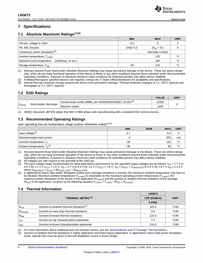
7 Specifications
7.1 Absolute Maximum Ratings (1) (2)
MIN MAX UNITVIN pin: voltage to GND –0.2 6 VFB, SW, EN pins GND−0.2 (VIN + 0.2 VContinuous power dissipation (3) Internally LimitedJunction temperature, TJ-MAX 125 °CMaximum lead temperature (soldering, 10 sec.) 260 °CStorage temperature, Tstg –65 150 °C
(1) JEDEC document JEP155 states that 500-V HBM allows safe manufacturing with a standard ESD control process.
7.2 ESD RatingsVALUE UNIT
V(ESD) Electrostatic dischargeHuman-body model (HBM), per ANSI/ESDA/JEDEC JS-001 (1) ±2000
VMachine model ±200
(1) Stresses beyond those listed under Absolute Maximum Ratings may cause permanent damage to the device. These are stress ratingsonly, which do not imply functional operation of the device at these or any other conditions beyond those indicated under RecommendedOperating Conditions. Exposure to absolute-maximum-rated conditions for extended periods may affect device reliability.
(2) All voltages are with respect to the potential at the GND pin.(3) The input voltage range recommended for ideal applications performance for the specified output voltages are as follows: VIN = 2.7 V to
4.5 V for 1.1 V ≤ VOUT < 1.5 V; VIN = 2.7 V to 5.5 V for 1.5 V ≤ VOUT < 1.8 V; VIN = (VOUT + VDROPOUT) to 5.5 V for 1.8 V ≤ VOUT ≤ 3.3 Vwhere VDROPOUT = ILOAD × (RDSON, PFET + RINDUCTOR)
(4) In applications where high power dissipation and/or poor package resistance is present, the maximum ambient temperature may have tobe derated. Maximum ambient temperature (TA-MAX) is dependent on the maximum operating junction temperature (TJ-MAX), themaximum power dissipation of the device in the application (PD-MAX) and the junction to ambient thermal resistance of the package(RθJA) in the application, as given by the following equation:TA-MAX = TJ-MAX− (RθJA × PD-MAX).
7.3 Recommended Operating Ratingsover operating free-air temperature range (unless otherwise noted) (1) (2)
MIN NOM MAX UNITInput voltage (3) 2.7 5.5 VRecommended load current 0 350 mAJunction temperature, TJ –30 125 °CAmbient temperature, TA
(4) –30 85 °C
(1) For more information about traditional and new thermal metrics, see the Semiconductor and IC Package Thermal Metrics.(2) Junction-to-ambient thermal resistance is highly application and board layout dependent. In applications where high power dissipation
exists, special care must be given to thermal dissipation issues in board design.
7.4 Thermal Information
THERMAL METRIC (1)LM3673
UNITYZR (DSBGA)5 PINS
RθJA Junction-to-ambient thermal resistance (2) 181.0 °C/WRθJC(top) Junction-to-case (top) thermal resistance 0.9 °C/WRθJB Junction-to-board thermal resistance 110.3 °C/WψJT Junction-to-top characterization parameter 7.4 °C/WψJB Junction-to-board characterization parameter 110.3 °C/W

5
LM3673www.ti.com SNVS434M –JULY 2006–REVISED NOVEMBER 2016
Product Folder Links: LM3673
Submit Documentation FeedbackCopyright © 2006–2016, Texas Instruments Incorporated
(1) All voltages are with respect to the potential at the GND pin.(2) Minimum and maximum limits are specified by design, test or statistical analysis. Typical numbers are not verified, but do represent the
most likely norm.(3) The parameters in the electrical characteristic table are tested at VIN= 3.6 V unless otherwise specified. For performance over the input
voltage range refer to datasheet curves.(4) The input voltage range recommended for ideal applications performance for the specified output voltages are as follows: VIN = 2.7 V to
4.5 V for 1.1 V ≤ VOUT < 1.5 V; VIN = 2.7 V to 5.5 V for 1.5 V ≤ VOUT < 1.8 V; VIN = (VOUT+ VDROPOUT) to 5.5 V for 1.8 V ≤ VOUT ≤ 3.3 V,where VDROPOUT = ILOAD × (RDSON, PFET + RINDUCTOR).
(5) Test condition: for VOUT less than 2.5 V, VIN = 3.6 V; for VOUT greater than or equal to 2.5 V, VIN = VOUT + 1 V.(6) Refer to for closed-loop data and its variation with regards to supply voltage and temperature. Electrical Characteristics reflects open-
loop data (FB = 0 V and current drawn from SW pin ramped up until cycle-by-cycle current limit is activated). Closed-loop current limit isthe peak inductor current measured in the application circuit by increasing output current until output voltage drops by 10%.
7.5 Electrical CharacteristicsTypical limits apply for TJ = 25°C. Unless otherwise specified, minimum and maximum limits apply over the full operatingambient temperature range (−30°C ≤ TA ≤ +85°C). Unless otherwise noted, specifications apply to the LM3673TL with VIN =EN = 3.6 V. (1) (2) (3)
PARAMETER TEST CONDITIONS MIN TYP MAX UNITVIN Input voltage See (4) 2.7 5.5 V
VFB
Feedback voltage (fixed /ADJ)
PWM mode (5)–2.5% 2.5%
Line regulation 2.7 V ≤ VIN ≤ 5.5 VIOUT = 20 mA 0.025 %/V
Load regulation 150 mA ≤ IOUT ≤ 350 mAVIN= 3.6 V 0.0015 %/mA
VREF Internal reference voltage 0.5 VISHDN Shutdown supply current EN = 0V 0.01 1 µA
IQDC bias current into VIN No load, device is not switching (FB forced
higher than programmed output voltage) 16 35 µA
RDSON (P) Pin-pin resistance for PFET VIN= VGS= 3.6 V, TA = 25°C 350 450 mΩRDSON (N) Pin-pin resistance for NFET VIN= VGS= 3.6 V, TA = 25°C 150 250 mΩILIM Switch peak current limit Open loop (6) 590 750 855 mAVIH Logic high input 1 VVIL Logic low input 0.4 VIEN Enable (EN) input current 0.01 1 µAƒOSC Internal oscillator frequency PWM mode (5) 1.6 2 2.6 MHz

-40 -20 0 20 40 60 80 100
TEMPERATURE (°C)
CU
RR
EN
T L
IMIT
(m
A)
VIN = 2.7V
VIN = 3.6V
VIN = 4.5V VIN = 3.6V
VIN = 4.5V
VIN = 2.7V
VIN = 2.7V
650
700
750
800
850
900
950Closed Loop = SolidOpen Loop = Dash
-10 10 30 50 70 90 110
TEMPERATURE (oC)
100
150
200
250
300
350
400
450
500
550
600
RD
S(O
N) (
m:
)
-30
NFET
VIN = 4.5V
PFET
VIN = 2.7V
VIN = 4.5VVIN = 3.6V
VIN = 3.6V
VIN = 2.7V
-10 10 30 50 70 90
TEMPERATURE (°C)
0.00
0.05
0.10
0.15
0.20
0.25
0.30
0.35
0.40
SH
UT
DO
WN
CU
RR
EN
T (P
A)
-30
EN = GND
VIN = 3.6V
VIN = 2.7V
VIN = 5.5V
3.0 3.5 4.0 4.5 5.0 5.5 6.0
SUPPLY VOLTAGE (V)
10
12
14
16
18
20
QU
IES
CE
NT
CU
RR
EN
T (P
A)
2.5
TA = 85°C
EN = VIN
IOUT = 0 mA
TA = 25°C
TA = -30°C
6
LM3673SNVS434M –JULY 2006–REVISED NOVEMBER 2016 www.ti.com
Product Folder Links: LM3673
Submit Documentation Feedback Copyright © 2006–2016, Texas Instruments Incorporated
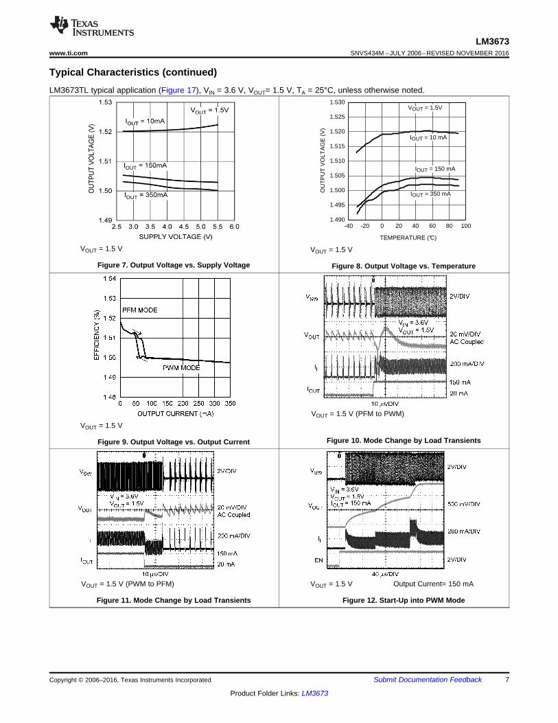
7.6 Typical CharacteristicsLM3673TL typical application (Figure 17), VIN = 3.6 V, VOUT= 1.5 V, TA = 25°C, unless otherwise noted.
Figure 1. Quiescent Supply Current vs. Supply Voltage Figure 2. Shutdown Current vs. Temperature
Figure 3. Feedback Bias Current vs. Temperature Figure 4. Switching Frequency vs. Temperature
Figure 5. RDSON vs. Temperature Figure 6. Open/Closed Loop Current Limit vs. Temperature
VOUT = 1.5V
IOUT = 10 mA
IOUT = 150 mA
IOUT = 350 mAOU
TP
UT
VO
LTA
GE
(V
)
TEMPERATURE (°C)
-40 -20 0 20 40 60 80 1001.490
1.495
1.500
1.505
1.510
1.515
1.520
1.525
1.530
7
LM3673www.ti.com SNVS434M –JULY 2006–REVISED NOVEMBER 2016
Product Folder Links: LM3673
Submit Documentation FeedbackCopyright © 2006–2016, Texas Instruments Incorporated
Typical Characteristics (continued)LM3673TL typical application (Figure 17), VIN = 3.6 V, VOUT= 1.5 V, TA = 25°C, unless otherwise noted.
VOUT = 1.5 V
Figure 7. Output Voltage vs. Supply Voltage
VOUT = 1.5 V
Figure 8. Output Voltage vs. Temperature
VOUT = 1.5 V
Figure 9. Output Voltage vs. Output Current
VOUT = 1.5 V (PFM to PWM)
Figure 10. Mode Change by Load Transients
VOUT = 1.5 V (PWM to PFM)
Figure 11. Mode Change by Load Transients
VOUT = 1.5 V Output Current= 150 mA
Figure 12. Start-Up into PWM Mode

8
LM3673SNVS434M –JULY 2006–REVISED NOVEMBER 2016 www.ti.com
Product Folder Links: LM3673
Submit Documentation Feedback Copyright © 2006–2016, Texas Instruments Incorporated
Typical Characteristics (continued)LM3673TL typical application (Figure 17), VIN = 3.6 V, VOUT= 1.5 V, TA = 25°C, unless otherwise noted.
VOUT = 1.5 V Output Current= 5 mA
Figure 13. Start-Up into PFM Mode

2-MHzOscillator
SoftStart
RampGenerator
ThermalShutdown
UndervoltageLockout
FrequencyCompensation
+-
ErrorAmp
Control Logic Driver
Current LimitComparator
Ref1
PFM CurrentComparator
Ref2
SW
Zero CrossingComparator
FB
EN VIN
PWM Comparator
pfm_low
pfm_hi
GND
Bandgap
+-
VCOMP
1 V
Fixed Version
ADJ Version
+-
0.5 V
+-
+-
+
-
VREF
9
LM3673www.ti.com SNVS434M –JULY 2006–REVISED NOVEMBER 2016
Product Folder Links: LM3673
Submit Documentation FeedbackCopyright © 2006–2016, Texas Instruments Incorporated
8 Detailed Description
8.1 OverviewThe LM3673, a high-efficiency step-down DC-DC switching buck converter, delivers a constant voltage from asingle Li-Ion battery and input voltage ranging from 2.7 V to 5.5 V to portable devices such as cell phones andPDAs. Using a voltage mode architecture with synchronous rectification, the LM3673 has the ability to deliver upto 350 mA depending on the input voltage, output voltage, ambient temperature and the inductor chosen.
There are three modes of operation depending on the current required: pulse width modulation (PWM), pulsefrequency modulation (PFM), and shutdown. The device operates in PWM mode at load current of approximately80 mA or higher. Lighter load current cause the device to automatically switch into PFM for reduced currentconsumption (IQ = 16 µA typical) and a longer battery life. Shutdown mode turns off the device, offering thelowest current consumption (ISHUTDOWN = 0.01 µA typical).
Additional features include soft-start, undervoltage protection, current overload protection, and thermal shutdownprotection. As shown in Figure 17, only three external power components are required for implementation. Thepart uses an internal reference voltage of 0.5 V. It is recommended to keep the part in shutdown until the inputvoltage is 2.7 V or higher.
8.2 Functional Block Diagram

VOUT
TIME (200 ns/DIV)
200 mA/DIVIL
VSW 2V/DIV
10 mV/DIVAC Coupled
VIN = 3.6V
VOUT = 1.5VIOUT = 150 mA
10
LM3673SNVS434M –JULY 2006–REVISED NOVEMBER 2016 www.ti.com
Product Folder Links: LM3673
Submit Documentation Feedback Copyright © 2006–2016, Texas Instruments Incorporated
8.3 Feature Description
8.3.1 Circuit OperationDuring the first portion of each switching cycle, the control block in the LM3673 turns on the internal PFETswitch. This allows current to flow from the input through the inductor to the output filter capacitor and load. Theinductor limits the current to a ramp with a slope of (VIN – VOUT) / L by storing energy in a magnetic field.
During the second portion of each cycle, the controller turns the PFET switch off, blocking current flow from theinput, and then turns the NFET synchronous rectifier on. The inductor draws current from ground through theNFET to the output filter capacitor and load, which ramps the inductor current down with a slope of –VOUT / L.
The output filter stores charge when the inductor current is high, and releases it when inductor current is low,smoothing the voltage across the load.
The output voltage is regulated by modulating the PFET switch on time to control the average current sent to theload. The effect is identical to sending a duty-cycle modulated rectangular wave formed by the switch andsynchronous rectifier at the SW pin to a low-pass filter formed by the inductor and output filter capacitor. Theoutput voltage is equal to the average voltage at the SW pin.
8.3.2 PWM OperationDuring PWM operation the converter operates as a voltage-mode controller with input voltage feed forward. Thisallows the converter to achieve good load and line regulation. The DC gain of the power stage is proportional tothe input voltage. To eliminate this dependence, feed forward inversely proportional to the input voltage isintroduced.
While in PWM mode, the output voltage is regulated by switching at a constant frequency and then modulatingthe energy per cycle to control power to the load. At the beginning of each clock cycle the PFET switch is turnedon and the inductor current ramps up until the comparator trips and the control logic turns off the switch. Thecurrent limit comparator can also turn off the switch in case the current limit of the PFET is exceeded. Then theNFET switch is turned on and the inductor current ramps down. The next cycle is initiated by the clock turning offthe NFET and turning on the PFET.
Figure 14. Typical PWM Operation
8.3.3 Internal Synchronous RectificationWhile in PWM mode, the LM3673 uses an internal NFET as a synchronous rectifier to reduce rectifier forwardvoltage drop and associated power loss. Synchronous rectification provides a significant improvement inefficiency whenever the output voltage is relatively low compared to the voltage drop across an ordinary rectifierdiode.

VOUT
TIME (4 Ps/DIV)
200 mA/DIVIL
VSW 2V/DIV
20 mV/DIVAC Coupled
VIN = 3.6VVOUT = 1.5V
IOUT = 20 mA
11
LM3673www.ti.com SNVS434M –JULY 2006–REVISED NOVEMBER 2016
Product Folder Links: LM3673
Submit Documentation FeedbackCopyright © 2006–2016, Texas Instruments Incorporated
Feature Description (continued)8.3.4 Current LimitingA current limit feature allows the LM3673 to protect itself and external components during overload conditions.PWM mode implements current limiting using an internal comparator that trips at 750 mA (typical). If the output isshorted to ground the device enters a timed current limit mode where the NFET is turned on for a longer durationuntil the inductor current falls below a low threshold. This allows the inductor current more time to decay, therebypreventing runaway.
8.3.5 Soft StartThe LM3673 has a soft-start circuit that limits in-rush current during start-up. During start-up the switch currentlimit is increased in steps. Soft start is activated only if EN goes from logic low to logic high after VIN reaches 2.7V. Soft start is implemented by increasing switch current limit in steps of 70 mA, 140 mA, 280 mA, and 750 mA(typical switch current limit). The start-up time thereby depends on the output capacitor and load current. Typicalstart-up time with a 10-µF output capacitor and 150-mA load is 280 µs; with a 5-mA load start-up time is 240 µs.
8.3.6 Low Drop Out Operation (LDO)The LM3673-ADJ can operate at 100% duty cycle (no switching; PMOS switch completely on) for LDO support ofthe output voltage. In this way the output voltage is controlled down to the lowest possible input voltage. Whenthe device operates near 100% duty cycle, output voltage ripple is approximately 25 mV.
The minimum input voltage needed to support the output voltage is:VIN, MIN = ILOAD × (RDSON, PFET + RINDUCTOR) + VOUT
where• ILOAD: Load current• RDSON, PFET: Drain-to-source resistance of PFET switch in the triode region• RINDUCTOR: Inductor resistance (1)
8.4 Device Functional Modes
8.4.1 PFM OperationAt very light load, the converter enters PFM mode and operates with reduced switching frequency and supplycurrent to maintain high efficiency.
The part automatically transitions into PFM mode when either of two conditions occurs for a duration of 32 ormore clock cycles:• The NFET current reaches zero.• The peak PMOS switch current drops below the IMODE level (typically IMODE < 30 mA + VIN / 42 Ω ).
Figure 15. Typical PFM Operation

High PFM Threshold~1.017*Vout
Low1 PFM Threshold~1.006*Vout
PFM Mode at Light Load
PWM Mode at Moderate to Heavy
Loads
Pfet onuntil
Ipfm limitreached
Nfet ondrains
inductorcurrent
untilI inductor = 0
High PFMVoltage
Thresholdreached,go into
sleep mode
Low PFMThreshold,
turn onPFET
Current loadincreases,draws Vout
towardsLow2 PFMThreshold
Low2 PFM Threshold,switch back to PWMmode
Load current increases
Low2 PFM ThresholdVout
Z-Axis
Z-
Axis
12
LM3673SNVS434M –JULY 2006–REVISED NOVEMBER 2016 www.ti.com
Product Folder Links: LM3673
Submit Documentation Feedback Copyright © 2006–2016, Texas Instruments Incorporated
Device Functional Modes (continued)During PFM operation, the converter positions the output voltage slightly higher than the nominal output voltageduring PWM operation, allowing additional headroom for voltage drop during a load transient from light to heavyload. The PFM comparators sense the output voltage via the FB pin and control the switching of the output FETssuch that the output voltage ramps from approximately 0.6% to approximately 1.7% above the nominal PWMoutput voltage. If the output voltage is below the high PFM comparator threshold, the PMOS power switch isturned on. It remains on until the output voltage reaches the high PFM threshold or the peak current exceeds theIPFM level set for PFM mode. The typical peak current in PFM mode is: IPFM = 112 mA + VIN / 27 Ω .
Once the PMOS power switch is turned off, the NMOS power switch is turned on until the inductor current rampsto zero. When the NMOS zero-current condition is detected, the NMOS power switch is turned off. If the outputvoltage is below the high PFM comparator threshold (see Figure 16), the PMOS switch is again turned on andthe cycle is repeated until the output reaches the desired level. Once the output reaches the high PFM threshold,the NMOS switch is turned on briefly to ramp the inductor current to zero and then both output switches areturned off and the part enters an extremely low power mode. Quiescent supply current during this sleep mode is16 µA (typical), which allows the device to achieve high efficiency under extremely light load conditions.
If the load current increases during PFM mode (see Figure 16) causing the output voltage to fall below the Low 2PFM threshold, the device automatically transitions into fixed-frequency PWM mode. When VIN = 2.7 V, thedevice transitions from PWM mode to PFM mode at approximately 35-mA output current and from PFM mode toPWM mode at approximately 85 mA. When VIN = 3.6 V, PWM-to-PFM transition happens at approximately 50mA and PFM-to-PWM transition happens at approximately 100 mA. When VIN = 4.5 V, PWM-to-PFM transitionhappens at approximately 65 mA and PFM-to-PWM transition happens at approximately 115 mA.
Figure 16. Operation in PFM Mode and Transfer to PWM Mode
8.4.2 Shutdown ModeSetting the EN input pin low (< 0.4 V) places the LM3673 in shutdown mode. During shutdown the PFET switch,NFET switch, reference, control, and bias circuitry of the LM3673 are turned off. Setting EN high (> 1 V) enablesnormal operation. Setting the EN pin low is recommended to turn off the LM3673 during system power up andundervoltage conditions when the supply is less than 2.7 V. Do not leave the EN pin floating.
1
2
5
43
VIN SW
FBEN
GND
L1: 2.2 µH VOUT
COUT
10 µF
CIN
4.7 µFLM3673-
ADJ
VIN
2.7 V to 5.5 V
R1
R2
C1
C2
1
2
5
43
VIN SW
FBEN
GND
L1: 2.2 µHVOUT
COUT
10 µFCIN
4.7 µFLM3673
VIN
2.7 V to 5.5 V
13
LM3673www.ti.com SNVS434M –JULY 2006–REVISED NOVEMBER 2016
Product Folder Links: LM3673
Submit Documentation FeedbackCopyright © 2006–2016, Texas Instruments Incorporated
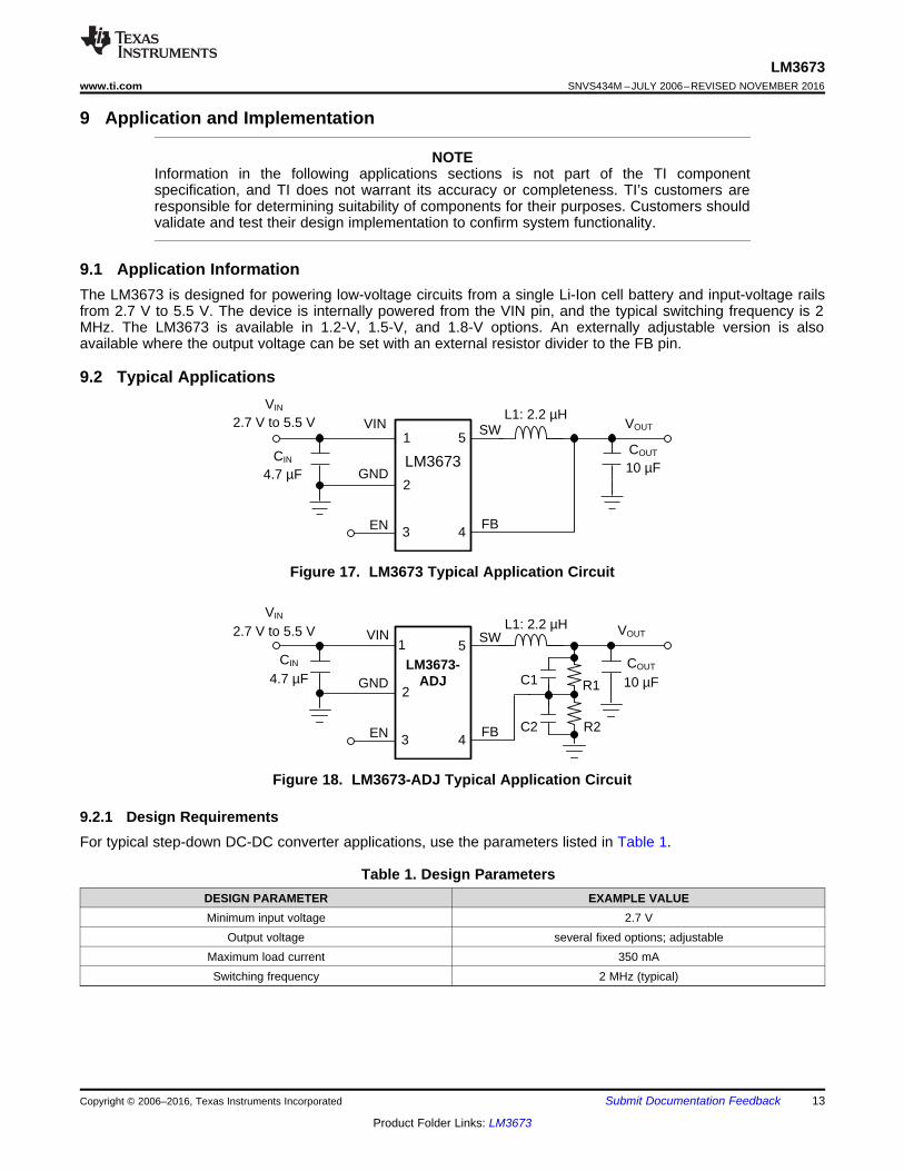
9 Application and Implementation
NOTEInformation in the following applications sections is not part of the TI componentspecification, and TI does not warrant its accuracy or completeness. TI’s customers areresponsible for determining suitability of components for their purposes. Customers shouldvalidate and test their design implementation to confirm system functionality.
9.1 Application InformationThe LM3673 is designed for powering low-voltage circuits from a single Li-Ion cell battery and input-voltage railsfrom 2.7 V to 5.5 V. The device is internally powered from the VIN pin, and the typical switching frequency is 2MHz. The LM3673 is available in 1.2-V, 1.5-V, and 1.8-V options. An externally adjustable version is alsoavailable where the output voltage can be set with an external resistor divider to the FB pin.
9.2 Typical Applications
Figure 17. LM3673 Typical Application Circuit
Figure 18. LM3673-ADJ Typical Application Circuit
9.2.1 Design RequirementsFor typical step-down DC-DC converter applications, use the parameters listed in Table 1.
Table 1. Design ParametersDESIGN PARAMETER EXAMPLE VALUEMinimum input voltage 2.7 V
Output voltage several fixed options; adjustableMaximum load current 350 mASwitching frequency 2 MHz (typical)

Fp =1
2 * S * (R1 R2) * (C1+C2)
Fz =1
(2 * S * R1 * C1)
C2 =1
(2 * S * R2 * 45 kHz)
C1 =1
(2 * S * R1 * 45 kHz)
VOUT = VFB 1 +R1
R2 ¹·
©§
14
LM3673SNVS434M –JULY 2006–REVISED NOVEMBER 2016 www.ti.com
Product Folder Links: LM3673
Submit Documentation Feedback Copyright © 2006–2016, Texas Instruments Incorporated
9.2.2 Detailed Design Procedure
9.2.2.1 Output Voltage Selection for LM3673-ADJThe output voltage of the adjustable device can be programmed through the resistor network connected fromVOUT to FB, then to GND. VOUT is adjusted to make the voltage at FB equal to 0.5 V. The resistor from FB toGND (R2) must be 200 kΩ to keep the current drawn through this network well below the 16-µA quiescentcurrent level (PFM mode) but large enough that it is not susceptible to noise. If R2 is 200 kΩ, and VFB is 0.5 V,the current through the resistor feedback network is 2.5 µA. The output voltage of the adjustable device rangesfrom 1.1 V to 3.3 V.
The formula for output voltage selection is:
where• VOUT: output voltage (V)• VFB : feedback voltage = 0.5 V• R1: feedback resistor from VOUT to FB• R2: feedback resistor from FB to GND (2)
For any output voltage greater than or equal to 1.1 V, a zero must be added around 45 kHz for stability. Theformula for calculation of C1 is:
(3)
For output voltages higher than 2.5 V, a pole must be placed at 45 kHz as well. If the pole and zero are at thesame frequency the formula for calculation of C2 is:
(4)
The formula for location of zero and pole frequency created by adding C1 and C2 is shown in Equation 5 andEquation 6. By adding C1, a zero as well as a higher frequency pole is introduced.
(5)
(6)
See Table 2.

¸¹
ᬩ
§
f
1
L2
!ISAT IOUTMAX + IRIPPLE
where IRIPPLE =VOUT
VIN¸¹
ᬩ
§¸¹
ᬩ
§VIN - VOUT
15
LM3673www.ti.com SNVS434M –JULY 2006–REVISED NOVEMBER 2016
Product Folder Links: LM3673
Submit Documentation FeedbackCopyright © 2006–2016, Texas Instruments Incorporated
(1) Circuit of Typical Application Circuit for ADJ Version.
Table 2. LM3673-ADJ Configurations For Various VOUT(1)
VOUT(V) R1(kΩ) R2 (kΩ) C1 (pF) C2 (pF) L (µH) CIN (µF) COUT (µF)1.1 240 200 15 None 2.2 4.7 101.2 280 200 12 None 2.2 4.7 101.3 320 200 12 None 2.2 4.7 101.5 357 178 10 None 2.2 4.7 101.6 442 200 8.2 None 2.2 4.7 101.7 432 178 8.2 None 2.2 4.7 101.8 464 178 8.2 None 2.2 4.7 10
1.875 523 191 6.8 None 2.2 4.7 102.5 402 100 8.2 None 2.2 4.7 102.8 464 100 8.2 33 2.2 4.7 103.3 562 100 6.8 33 2.2 4.7 10
9.2.2.2 Inductor SelectionThere are two main considerations when choosing an inductor; the inductor must not saturate, and the inductorcurrent ripple must be small enough to achieve the desired output voltage ripple. Different saturation currentrating specifications are followed by different manufacturers so attention must be given to details. Saturationcurrent ratings are typically specified at 25°C. However, ratings at the maximum ambient temperature ofapplication should be requested from the manufacturer. The minimum value of inductance to ensure goodperformance is 1.76 µH at ILIM (typical) DC current over the ambient temperature range. Shielded inductorsradiate less noise and are preferred.
There are two methods to choose the inductor saturation current rating.
9.2.2.2.1 Method 1
The saturation current must be greater than the sum of the maximum load current and the worst case average topeak inductor current. This can be written as:
where• IRIPPLE: average to peak inductor current• IOUTMAX: maximum load current (350 mA)• VIN: maximum input voltage in application• L : min inductor value including worst case tolerances (30% drop can be considered for Method 1)• ƒ : minimum switching frequency (1.6 MHz)• VOUT: output voltage (7)
9.2.2.2.2 Method 2
A more conservative and recommended approach is to choose an inductor that has a saturation current ratinggreater than the maximum current limit of 855 mA.
A 2.2-µH inductor with a saturation current rating of at least 855 mA is recommended for most applications.Resistance of the inductor must be less than 0.3 Ω for good efficiency. Table 3 lists suggested inductors andsuppliers. For low-cost applications, an unshielded bobbin inductor could be considered. For noise criticalapplications, a toroidal or shielded-bobbin inductor must be used. A good practice is to lay out the board withoverlapping footprints of both types for design flexibility. This allows substitution of a low-noise shielded inductor,in the event that noise from low-cost bobbin models is unacceptable.

VPP-C = 4*f*C
IRIPPLE
IRMS = IOUTMAX
The worst case is when VIN = 2 VOUT
(VIN - VOUT) VOUT
L f IOUTMAX VIN
r =
VOUT
VIN
r2
121 - +
VOUT
VIN¸¹
ᬩ
§
16
LM3673SNVS434M –JULY 2006–REVISED NOVEMBER 2016 www.ti.com
Product Folder Links: LM3673
Submit Documentation Feedback Copyright © 2006–2016, Texas Instruments Incorporated
9.2.2.3 Input Capacitor SelectionA ceramic input capacitor of 4.7 µF, 6.3 V is sufficient for most applications. Place the input capacitor as close aspossible to the VIN pin of the device. A larger value may be used for improved input voltage filtering. Use X7R orX5R types; do not use Y5V. DC bias characteristics of ceramic capacitors must be considered when selectingcase sizes like 0805 and 0603. The minimum input capacitance to ensure good performance is 2.2 µF at 3-V DCbias; 1.5 µF at 5-V DC bias including tolerances and over ambient temperature range. The input filter capacitorsupplies current to the PFET switch of the LM3673 in the first half of each cycle and reduces voltage rippleimposed on the input power source. The low ESR of a ceramic capacitor provides the best noise filtering of theinput voltage spikes due to this rapidly changing current. Select a capacitor with sufficient ripple current rating.The input current ripple can be calculated as:
(8)
Table 3. Suggested Inductors and Their SuppliersMODEL VENDOR DIMENSIONS L × W × H (mm) DCR (maximum)
COILBRL2518T2R2M Taiyo Yuden 2.5 × 1.8 × 1.2 135 mΩDO3314-222MX Coilcraft 3.3 × 3.3 × 1.4 200 mΩLPO3310-222MX Coilcraft 3.3 × 3.3 × 1 150 mΩCDRH2D14-2R2 Sumida 3.2 × 3.2 × 1.55 94 mΩ
CHIPKSLI-2520101AG2R2 Hitachi Metals 2.5 × 2 × 1.0 115 mΩ
LQM31PN2R2M00 Murata 3.2 × 1.6 × 0.95 220 mΩLQM2HPN2R2MJ0 Murata 2.5 × 2 × 1.2 160 mΩ
9.2.2.4 Output Capacitor SelectionA ceramic output capacitor of 10 µF, 6.3 V is sufficient for most applications. Use X7R or X5R types; do not useY5V. DC bias characteristics of ceramic capacitors must be considered when selecting case sizes like 0805 and0603. DC bias characteristics vary from manufacturer to manufacturer and DC bias curves should be requestedfrom them as part of the capacitor selection process.
The minimum output capacitance to ensure good performance is 5.75 µF at 1.8-V DC bias including tolerancesand over ambient temperature range. The output filter capacitor smoothes out current flow from the inductor tothe load, helps maintain a steady output voltage during transient load changes and reduces output voltage ripple.These capacitors must be selected with sufficient capacitance and sufficiently low ESR to perform thesefunctions.
The output voltage ripple is caused by the charging and discharging of the output capacitor and by the RESR andcan be calculated as:
Voltage peak-to-peak ripple due to capacitance can be expressed as follows:
(9)
Voltage peak-to-peak ripple due to ESR can be expressed as follows:VPP-ESR = (2 × IRIPPLE) × RESR
Because these two components are out of phase the root mean squared (RMS) value can be used to get anapproximate value of peak-to-peak ripple.

VPP-RMS = VPP-C2 + VPP-ESR
2
17
LM3673www.ti.com SNVS434M –JULY 2006–REVISED NOVEMBER 2016
Product Folder Links: LM3673
Submit Documentation FeedbackCopyright © 2006–2016, Texas Instruments Incorporated
The peak-to-peak ripple voltage, rms value can be expressed as follow:
(10)
The output voltage ripple is dependent on the inductor current ripple and the equivalent series resistance of theoutput capacitor (RESR).
The RESR is frequency dependent (as well as temperature dependent); make sure the value used for calculationsis at the switching frequency of the device.
Table 4. Suggested Capacitors and Their SuppliersMODEL TYPE VENDOR VOLTAGE RATING CASE SIZE inch (mm)
4.7 µF for CIN
C2012X5R0J475K Ceramic, X5R TDK 6.3 V 0805 (2012)JMK212BJ475K Ceramic, X5R Taiyo-Yuden 6.3 V 0805 (2012)
GRM21BR60J475K Ceramic, X5R Murata 6.3 V 0805 (2012)C1608X5R0J475K Ceramic, X5R TDK 6.3 V 0603 (1608)
10 µF for COUT
GRM21BR60J106K Ceramic, X5R Murata 6.3 V 0805 (2012)JMK212BJ106K Ceramic, X5R Taiyo-Yuden 6.3 V 0805 (2012)
C2012X5R0J106K Ceramic, X5R TDK 6.3 V 0805 (2012)C1608X5R0J106K Ceramic, X5R TDK 6.3 V 0603 (1608)
18
LM3673SNVS434M –JULY 2006–REVISED NOVEMBER 2016 www.ti.com
Product Folder Links: LM3673
Submit Documentation Feedback Copyright © 2006–2016, Texas Instruments Incorporated
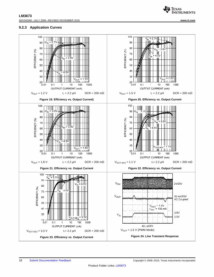
9.2.3 Application Curves
VOUT = 1.2 V L = 2.2 µH DCR = 200 mΩ
Figure 19. Efficiency vs. Output Current)
VOUT = 1.5 V L = 2.2 µH DCR = 200 mΩ
Figure 20. Efficiency vs. Output Current
VOUT = 1.8 V L = 2.2 µH DCR = 200 mΩ
Figure 21. Efficiency vs. Output Current
VOUT-ADJ = 1.1 V L= 2.2 µH DCR = 200 mΩ
Figure 22. Efficiency vs. Output Current
VOUT-ADJ = 3.3 V L= 2.2 µH DCR = 200 mΩ
Figure 23. Efficiency vs. Output Current
VOUT = 1.5 V (PWM Mode)
Figure 24. Line Transient Response

19
LM3673www.ti.com SNVS434M –JULY 2006–REVISED NOVEMBER 2016
Product Folder Links: LM3673
Submit Documentation FeedbackCopyright © 2006–2016, Texas Instruments Incorporated
VOUT = 1.5 V (PWM Mode)
Figure 25. Load Transient Response
VOUT = 1.5 V PFM Mode 0.5 mA to 50 mA
Figure 26. Load Transient Response
VOUT = 1.5 V PFM Mode 0.5 mA to 50 mA
Figure 27. Load Transient Response
10 Power Supply RecommendationsThe LM3673 requires a single supply input voltage. This voltage can range between 2.7 V to 5.5 V and must beable to supply enough current for a given application.
20
LM3673SNVS434M –JULY 2006–REVISED NOVEMBER 2016 www.ti.com
Product Folder Links: LM3673
Submit Documentation Feedback Copyright © 2006–2016, Texas Instruments Incorporated
11 Layout
11.1 Layout GuidelinesPC board layout is an important part of DC-DC converter design. Poor board layout can disrupt the performanceof a DC-DC converter and surrounding circuitry by contributing to EMI, ground bounce, and resistive voltage lossin the traces. These can send erroneous signals to the DC-DC converter device, resulting in poor regulation orinstability.
Good layout for the LM3673 can be implemented by following a few simple design rules below. Refer toFigure 28 for top layer board layout.1. Place the LM3673, inductor and filter capacitors close together and make the traces short. The traces
between these components carry relatively high switching currents and act as antennas. Following this rulereduces radiated noise. Special care must be given to place the input filter capacitor very close to the VINand GND pins.
2. Arrange the components so that the switching current loops curl in the same direction. During the first half ofeach cycle, current flows from the input filter capacitor through the LM3673 and inductor to the output filtercapacitor and back through ground, forming a current loop. In the second half of each cycle, current is pulledup from ground through the LM3673 by the inductor to the output filter capacitor and then back throughground forming a second current loop. Routing these loops so the current curls in the same directionprevents magnetic field reversal between the two half-cycles and reduces radiated noise.
3. Connect the ground pins of the LM3673 and filter capacitors together using generous component-sidecopper fill as a pseudo-ground plane. Then, connect this to the ground-plane (if one is used) with severalvias. This reduces ground-plane noise by preventing the switching currents from circulating through theground plane. It also reduces ground bounce at the LM3673 by giving it a low-impedance ground connection.
4. Use wide traces between the power components and for power connections to the DC-DC converter circuit.This reduces voltage errors caused by resistive losses across the traces.
5. Route noise sensitive traces, such as the voltage feedback path, away from noisy traces between the powercomponents. The voltage feedback trace must remain close to the LM3673 circuit and must be direct, butrouted opposite to noisy components. This reduces EMI radiated onto the own voltage feedback trace of theDC-DC converter. A good approach is to route the feedback trace on another layer and to have a groundplane between the top layer and layer on which the feedback trace is routed. For the adjustable deviceoption, it is also best to have the feedback dividers on the bottom layer.
6. Place noise sensitive circuitry, such as radio IF blocks, away from the DC-DC converter, CMOS digital blocksand other noisy circuitry. Interference with noise-sensitive circuitry in the system can be reduced throughdistance.
In mobile phones, for example, a common practice is to place the DC-DC converter on one corner of the board,arrange the CMOS digital circuitry around it (because this also generates noise), and then place sensitivepreamplifiers and IF stages on the diagonally opposing corner. Often, the sensitive circuitry is shielded with ametal pan and power to it is post-regulated to reduce conducted noise, using low-dropout linear regulators.

21
LM3673www.ti.com SNVS434M –JULY 2006–REVISED NOVEMBER 2016
Product Folder Links: LM3673
Submit Documentation FeedbackCopyright © 2006–2016, Texas Instruments Incorporated
11.2 Layout Example
Figure 28. LM3673 DSBGA Top Layer Board Layout
11.3 DSBGA Package Assembly and UseUse of the DSBGA package requires specialized board layout, precision mounting and careful re-flowtechniques, as detailed in Texas Instruments AN-1112 DSBGA Wafer Level Chip Scale Package. Refer to thesection Surface Mount Technology (SMD) Assembly Considerations. For best results in assembly, alignmentordinals on the PC board must be used to facilitate placement of the device. The pad style used with DSBGApackage must be the NSMD (non-solder mask defined) type. This means that the solder-mask opening is largerthan the pad size. This prevents a lip that otherwise forms if the solder-mask and pad overlap, from holding thedevice off the surface of the board and interfering with mounting. See SNVA009 for specific instructions how todo this. The 5-pin package used for LM3673 has 300-micron solder balls and requires 10.82 mils pads formounting on the circuit board. The trace to each pad must enter the pad with a 90° entry angle to prevent debrisfrom being caught in deep corners. Initially, the trace to each pad must be 7 mil wide, for a section approximately7 mil long or longer, as a thermal relief. Then each trace must neck up or down to its optimal width. Theimportant criteria is symmetry. This ensures the solder bumps on the LM3673 re-flow evenly and that the devicesolders level to the board. In particular, special attention must be paid to the pads for bumps A1 and A3,because VIN and GND are typically connected to large copper planes, inadequate thermal relief can result in lateor inadequate re-flow of these bumps.
The DSBGA package is optimized for the smallest possible size in applications with red or infrared opaquecases. Because the DSBGA package lacks the plastic encapsulation characteristic of larger devices, it isvulnerable to light. Backside metallization and/or epoxy coating, along with front-side shading by the printedcircuit board, reduce this sensitivity. However, the package has exposed die edges. In particular, DSBGAdevices are sensitive to light, in the red and infrared range, shining on the package’s exposed die edges.

22
LM3673SNVS434M –JULY 2006–REVISED NOVEMBER 2016 www.ti.com
Product Folder Links: LM3673
Submit Documentation Feedback Copyright © 2006–2016, Texas Instruments Incorporated
12 Device and Documentation Support
12.1 Device Support
12.1.1 Third-Party Products DisclaimerTI'S PUBLICATION OF INFORMATION REGARDING THIRD-PARTY PRODUCTS OR SERVICES DOES NOTCONSTITUTE AN ENDORSEMENT REGARDING THE SUITABILITY OF SUCH PRODUCTS OR SERVICESOR A WARRANTY, REPRESENTATION OR ENDORSEMENT OF SUCH PRODUCTS OR SERVICES, EITHERALONE OR IN COMBINATION WITH ANY TI PRODUCT OR SERVICE.
12.2 Documentation Support
12.2.1 Related DocumentationFor further information, see the following:
AN-1112 DSBGA Wafer Level Chip Scale Package
12.3 Receiving Notification of Documentation UpdatesTo receive notification of documentation updates, navigate to the device product folder on ti.com. In the upperright corner, click on Alert me to register and receive a weekly digest of any product information that haschanged. For change details, review the revision history included in any revised document.
12.4 Community ResourcesThe following links connect to TI community resources. Linked contents are provided "AS IS" by the respectivecontributors. They do not constitute TI specifications and do not necessarily reflect TI's views; see TI's Terms ofUse.
TI E2E™ Online Community TI's Engineer-to-Engineer (E2E) Community. Created to foster collaborationamong engineers. At e2e.ti.com, you can ask questions, share knowledge, explore ideas and helpsolve problems with fellow engineers.
Design Support TI's Design Support Quickly find helpful E2E forums along with design support tools andcontact information for technical support.
12.5 TrademarksE2E is a trademark of Texas Instruments.All other trademarks are the property of their respective owners.
12.6 Electrostatic Discharge CautionThis integrated circuit can be damaged by ESD. Texas Instruments recommends that all integrated circuits be handled withappropriate precautions. Failure to observe proper handling and installation procedures can cause damage.
ESD damage can range from subtle performance degradation to complete device failure. Precision integrated circuits may be moresusceptible to damage because very small parametric changes could cause the device not to meet its published specifications.
12.7 GlossarySLYZ022 — TI Glossary.
This glossary lists and explains terms, acronyms, and definitions.
13 Mechanical, Packaging, and Orderable InformationThe following pages include mechanical, packaging, and orderable information. This information is the mostcurrent data available for the designated devices. This data is subject to change without notice and revision ofthis document. For browser-based versions of this data sheet, refer to the left-hand navigation.

PACKAGE OPTION ADDENDUM
www.ti.com 23-Aug-2017
Addendum-Page 1
PACKAGING INFORMATION
Orderable Device Status(1)
Package Type PackageDrawing
Pins PackageQty
Eco Plan(2)
Lead/Ball Finish(6)
MSL Peak Temp(3)
Op Temp (°C) Device Marking(4/5)
Samples
LM3673TL-1.2/NOPB ACTIVE DSBGA YZR 5 250 Green (RoHS& no Sb/Br)
SNAGCU Level-1-260C-UNLIM -30 to 85 1
LM3673TL-1.5/NOPB ACTIVE DSBGA YZR 5 250 Green (RoHS& no Sb/Br)
SNAGCU Level-1-260C-UNLIM -30 to 85 H
LM3673TL-1.8/NOPB ACTIVE DSBGA YZR 5 250 Green (RoHS& no Sb/Br)
SNAGCU Level-1-260C-UNLIM -30 to 85 F
LM3673TL-ADJ/NOPB ACTIVE DSBGA YZR 5 250 Green (RoHS& no Sb/Br)
SNAGCU Level-1-260C-UNLIM -30 to 85 R
LM3673TLX-1.2/NOPB ACTIVE DSBGA YZR 5 3000 Green (RoHS& no Sb/Br)
SNAGCU Level-1-260C-UNLIM -30 to 85 1
LM3673TLX-1.8/NOPB ACTIVE DSBGA YZR 5 3000 Green (RoHS& no Sb/Br)
SNAGCU Level-1-260C-UNLIM -30 to 85 F
LM3673TLX-ADJ/NOPB ACTIVE DSBGA YZR 5 3000 Green (RoHS& no Sb/Br)
SNAGCU Level-1-260C-UNLIM -30 to 85 R
(1) The marketing status values are defined as follows:ACTIVE: Product device recommended for new designs.LIFEBUY: TI has announced that the device will be discontinued, and a lifetime-buy period is in effect.NRND: Not recommended for new designs. Device is in production to support existing customers, but TI does not recommend using this part in a new design.PREVIEW: Device has been announced but is not in production. Samples may or may not be available.OBSOLETE: TI has discontinued the production of the device.
(2) RoHS: TI defines "RoHS" to mean semiconductor products that are compliant with the current EU RoHS requirements for all 10 RoHS substances, including the requirement that RoHS substancedo not exceed 0.1% by weight in homogeneous materials. Where designed to be soldered at high temperatures, "RoHS" products are suitable for use in specified lead-free processes. TI mayreference these types of products as "Pb-Free".RoHS Exempt: TI defines "RoHS Exempt" to mean products that contain lead but are compliant with EU RoHS pursuant to a specific EU RoHS exemption.Green: TI defines "Green" to mean the content of Chlorine (Cl) and Bromine (Br) based flame retardants meet JS709B low halogen requirements of <=1000ppm threshold. Antimony trioxide basedflame retardants must also meet the <=1000ppm threshold requirement.
(3) MSL, Peak Temp. - The Moisture Sensitivity Level rating according to the JEDEC industry standard classifications, and peak solder temperature.
(4) There may be additional marking, which relates to the logo, the lot trace code information, or the environmental category on the device.
(5) Multiple Device Markings will be inside parentheses. Only one Device Marking contained in parentheses and separated by a "~" will appear on a device. If a line is indented then it is a continuationof the previous line and the two combined represent the entire Device Marking for that device.
PACKAGE OPTION ADDENDUM
www.ti.com 23-Aug-2017
Addendum-Page 2
(6) Lead/Ball Finish - Orderable Devices may have multiple material finish options. Finish options are separated by a vertical ruled line. Lead/Ball Finish values may wrap to two lines if the finishvalue exceeds the maximum column width.
Important Information and Disclaimer:The information provided on this page represents TI's knowledge and belief as of the date that it is provided. TI bases its knowledge and belief on informationprovided by third parties, and makes no representation or warranty as to the accuracy of such information. Efforts are underway to better integrate information from third parties. TI has taken andcontinues to take reasonable steps to provide representative and accurate information but may not have conducted destructive testing or chemical analysis on incoming materials and chemicals.TI and TI suppliers consider certain information to be proprietary, and thus CAS numbers and other limited information may not be available for release.
In no event shall TI's liability arising out of such information exceed the total purchase price of the TI part(s) at issue in this document sold by TI to Customer on an annual basis.

TAPE AND REEL INFORMATION
*All dimensions are nominal
Device PackageType
PackageDrawing
Pins SPQ ReelDiameter
(mm)
ReelWidth
W1 (mm)
A0(mm)
B0(mm)
K0(mm)
P1(mm)
W(mm)
Pin1Quadrant
LM3673TL-1.2/NOPB DSBGA YZR 5 250 178.0 8.4 1.14 1.47 0.76 4.0 8.0 Q1
LM3673TL-1.5/NOPB DSBGA YZR 5 250 178.0 8.4 1.14 1.47 0.76 4.0 8.0 Q1
LM3673TL-1.8/NOPB DSBGA YZR 5 250 178.0 8.4 1.14 1.47 0.76 4.0 8.0 Q1
LM3673TL-ADJ/NOPB DSBGA YZR 5 250 178.0 8.4 1.14 1.47 0.76 4.0 8.0 Q1
LM3673TLX-1.2/NOPB DSBGA YZR 5 3000 178.0 8.4 1.14 1.47 0.76 4.0 8.0 Q1
LM3673TLX-1.8/NOPB DSBGA YZR 5 3000 178.0 8.4 1.14 1.47 0.76 4.0 8.0 Q1
LM3673TLX-ADJ/NOPB DSBGA YZR 5 3000 178.0 8.4 1.14 1.47 0.76 4.0 8.0 Q1
PACKAGE MATERIALS INFORMATION
www.ti.com 30-Nov-2016
Pack Materials-Page 1
*All dimensions are nominal
Device Package Type Package Drawing Pins SPQ Length (mm) Width (mm) Height (mm)
LM3673TL-1.2/NOPB DSBGA YZR 5 250 210.0 185.0 35.0
LM3673TL-1.5/NOPB DSBGA YZR 5 250 210.0 185.0 35.0
LM3673TL-1.8/NOPB DSBGA YZR 5 250 210.0 185.0 35.0
LM3673TL-ADJ/NOPB DSBGA YZR 5 250 210.0 185.0 35.0
LM3673TLX-1.2/NOPB DSBGA YZR 5 3000 210.0 185.0 35.0
LM3673TLX-1.8/NOPB DSBGA YZR 5 3000 210.0 185.0 35.0
LM3673TLX-ADJ/NOPB DSBGA YZR 5 3000 210.0 185.0 35.0
PACKAGE MATERIALS INFORMATION
www.ti.com 30-Nov-2016
Pack Materials-Page 2

MECHANICAL DATA
YZR0005xxx
www.ti.com
TLA05XXX (Rev C)
0.600±0.075
D
E
NOTES: A. All linear dimensions are in millimeters. Dimensioning and tolerancing per ASME Y14.5M-1994.B. This drawing is subject to change without notice.
4215043/A 12/12
D: Max =
E: Max =
1.413 mm, Min =
1.083 mm, Min =
1.352 mm
1.022 mm

IMPORTANT NOTICE
Texas Instruments Incorporated (TI) reserves the right to make corrections, enhancements, improvements and other changes to itssemiconductor products and services per JESD46, latest issue, and to discontinue any product or service per JESD48, latest issue. Buyersshould obtain the latest relevant information before placing orders and should verify that such information is current and complete.TI’s published terms of sale for semiconductor products (http://www.ti.com/sc/docs/stdterms.htm) apply to the sale of packaged integratedcircuit products that TI has qualified and released to market. Additional terms may apply to the use or sale of other types of TI products andservices.Reproduction of significant portions of TI information in TI data sheets is permissible only if reproduction is without alteration and isaccompanied by all associated warranties, conditions, limitations, and notices. TI is not responsible or liable for such reproduceddocumentation. Information of third parties may be subject to additional restrictions. Resale of TI products or services with statementsdifferent from or beyond the parameters stated by TI for that product or service voids all express and any implied warranties for theassociated TI product or service and is an unfair and deceptive business practice. TI is not responsible or liable for any such statements.Buyers and others who are developing systems that incorporate TI products (collectively, “Designers”) understand and agree that Designersremain responsible for using their independent analysis, evaluation and judgment in designing their applications and that Designers havefull and exclusive responsibility to assure the safety of Designers' applications and compliance of their applications (and of all TI productsused in or for Designers’ applications) with all applicable regulations, laws and other applicable requirements. Designer represents that, withrespect to their applications, Designer has all the necessary expertise to create and implement safeguards that (1) anticipate dangerousconsequences of failures, (2) monitor failures and their consequences, and (3) lessen the likelihood of failures that might cause harm andtake appropriate actions. Designer agrees that prior to using or distributing any applications that include TI products, Designer willthoroughly test such applications and the functionality of such TI products as used in such applications.TI’s provision of technical, application or other design advice, quality characterization, reliability data or other services or information,including, but not limited to, reference designs and materials relating to evaluation modules, (collectively, “TI Resources”) are intended toassist designers who are developing applications that incorporate TI products; by downloading, accessing or using TI Resources in anyway, Designer (individually or, if Designer is acting on behalf of a company, Designer’s company) agrees to use any particular TI Resourcesolely for this purpose and subject to the terms of this Notice.TI’s provision of TI Resources does not expand or otherwise alter TI’s applicable published warranties or warranty disclaimers for TIproducts, and no additional obligations or liabilities arise from TI providing such TI Resources. TI reserves the right to make corrections,enhancements, improvements and other changes to its TI Resources. TI has not conducted any testing other than that specificallydescribed in the published documentation for a particular TI Resource.Designer is authorized to use, copy and modify any individual TI Resource only in connection with the development of applications thatinclude the TI product(s) identified in such TI Resource. NO OTHER LICENSE, EXPRESS OR IMPLIED, BY ESTOPPEL OR OTHERWISETO ANY OTHER TI INTELLECTUAL PROPERTY RIGHT, AND NO LICENSE TO ANY TECHNOLOGY OR INTELLECTUAL PROPERTYRIGHT OF TI OR ANY THIRD PARTY IS GRANTED HEREIN, including but not limited to any patent right, copyright, mask work right, orother intellectual property right relating to any combination, machine, or process in which TI products or services are used. Informationregarding or referencing third-party products or services does not constitute a license to use such products or services, or a warranty orendorsement thereof. Use of TI Resources may require a license from a third party under the patents or other intellectual property of thethird party, or a license from TI under the patents or other intellectual property of TI.TI RESOURCES ARE PROVIDED “AS IS” AND WITH ALL FAULTS. TI DISCLAIMS ALL OTHER WARRANTIES ORREPRESENTATIONS, EXPRESS OR IMPLIED, REGARDING RESOURCES OR USE THEREOF, INCLUDING BUT NOT LIMITED TOACCURACY OR COMPLETENESS, TITLE, ANY EPIDEMIC FAILURE WARRANTY AND ANY IMPLIED WARRANTIES OFMERCHANTABILITY, FITNESS FOR A PARTICULAR PURPOSE, AND NON-INFRINGEMENT OF ANY THIRD PARTY INTELLECTUALPROPERTY RIGHTS. TI SHALL NOT BE LIABLE FOR AND SHALL NOT DEFEND OR INDEMNIFY DESIGNER AGAINST ANY CLAIM,INCLUDING BUT NOT LIMITED TO ANY INFRINGEMENT CLAIM THAT RELATES TO OR IS BASED ON ANY COMBINATION OFPRODUCTS EVEN IF DESCRIBED IN TI RESOURCES OR OTHERWISE. IN NO EVENT SHALL TI BE LIABLE FOR ANY ACTUAL,DIRECT, SPECIAL, COLLATERAL, INDIRECT, PUNITIVE, INCIDENTAL, CONSEQUENTIAL OR EXEMPLARY DAMAGES INCONNECTION WITH OR ARISING OUT OF TI RESOURCES OR USE THEREOF, AND REGARDLESS OF WHETHER TI HAS BEENADVISED OF THE POSSIBILITY OF SUCH DAMAGES.Unless TI has explicitly designated an individual product as meeting the requirements of a particular industry standard (e.g., ISO/TS 16949and ISO 26262), TI is not responsible for any failure to meet such industry standard requirements.Where TI specifically promotes products as facilitating functional safety or as compliant with industry functional safety standards, suchproducts are intended to help enable customers to design and create their own applications that meet applicable functional safety standardsand requirements. Using products in an application does not by itself establish any safety features in the application. Designers mustensure compliance with safety-related requirements and standards applicable to their applications. Designer may not use any TI products inlife-critical medical equipment unless authorized officers of the parties have executed a special contract specifically governing such use.Life-critical medical equipment is medical equipment where failure of such equipment would cause serious bodily injury or death (e.g., lifesupport, pacemakers, defibrillators, heart pumps, neurostimulators, and implantables). Such equipment includes, without limitation, allmedical devices identified by the U.S. Food and Drug Administration as Class III devices and equivalent classifications outside the U.S.TI may expressly designate certain products as completing a particular qualification (e.g., Q100, Military Grade, or Enhanced Product).Designers agree that it has the necessary expertise to select the product with the appropriate qualification designation for their applicationsand that proper product selection is at Designers’ own risk. Designers are solely responsible for compliance with all legal and regulatoryrequirements in connection with such selection.Designer will fully indemnify TI and its representatives against any damages, costs, losses, and/or liabilities arising out of Designer’s non-compliance with the terms and provisions of this Notice.
Mailing Address: Texas Instruments, Post Office Box 655303, Dallas, Texas 75265Copyright © 2017, Texas Instruments Incorporated


![SUBMERSIBLE SUMP PUMPS...SUBMERSIBLE SUMP PUMPS BEST ONE TECHNICAL DATA 60Hz 500 EBARA Pumps Europe S.p.A. Rev. G MOTOR DATA Three Phase Three Phase Three Phase [µF][V][µF][V] 110](https://img.pdfslide.net/doc/110x75/60a9122b6c35ec75147c6eec/submersible-sump-pumps-submersible-sump-pumps-best-one-technical-data-60hz-500.jpg)