Embed Size (px)
Citation preview
LMK01000
www.ti.com SNAS437G –FEBRUARY 2008–REVISED OCTOBER 2009
LMK01000 Family LMK01000 Family 1.6 GHz High Performance Clock Buffer, Divider, andDistributor
Check for Samples: LMK01000
1FEATURES • 3.15 to 3.45 V operation• Package: 48 pin LLP (7.0 x 7.0 x 0.8 mm)
2• 30 fs additive jitter (100 Hz to 20 MHz)• Dual clock inputs
LVDS LVPECLDevice• Programmable output channels (0 to 1600 Outputs Outputs
MHz) LMK01000 3 5
• External synchronization LMK01010 8 0
LMK01020 0 8• Pin compatible family of clocking devices
TARGET APPLICATIONS• High performance Clock Distribution• Wireless Infrastructure• Medical Imaging• Wired Communications• Test and Measurement• Military / Aerospace
DESCRIPTIONThe LMK01000 family provides an easy way to divide and distribute high performance clock signals throughoutthe system. These devices provide best-in-class noise performance and are designed to be pin-to-pin andfootprint compatible with LMK03000/LMK02000 family of precision clock conditioners.
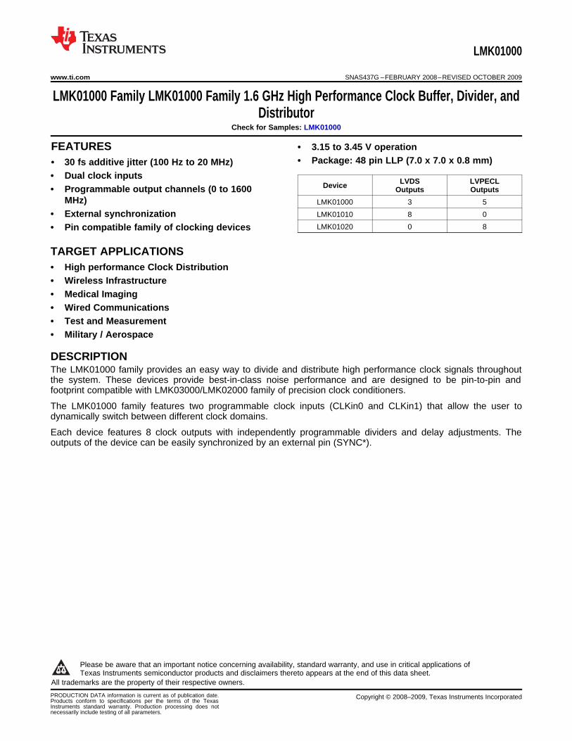
The LMK01000 family features two programmable clock inputs (CLKin0 and CLKin1) that allow the user todynamically switch between different clock domains.
Each device features 8 clock outputs with independently programmable dividers and delay adjustments. Theoutputs of the device can be easily synchronized by an external pin (SYNC*).
1
Please be aware that an important notice concerning availability, standard warranty, and use in critical applications ofTexas Instruments semiconductor products and disclaimers thereto appears at the end of this data sheet.
2All trademarks are the property of their respective owners.
PRODUCTION DATA information is current as of publication date. Copyright © 2008–2009, Texas Instruments IncorporatedProducts conform to specifications per the terms of the TexasInstruments standard warranty. Production processing does notnecessarily include testing of all parameters.
CLKin0
CLKin0*
CLKout0CLKout0*
CLKout1CLKout1*
CLKout2CLKout2*
CLKout3CLKout3*
CLKout4CLKout4*
CLKout5CLKout5*
CLKout6CLKout6*
CLKout7CLKout7*
DividerDelay
Mux
DividerDelay
Mux
DividerDelay
Mux
DividerDelay
Mux
DividerDelay
Mux
DividerDelay
Mux
DividerDelay
Mux
DividerDelay
Mux
Distribution PathCLK
DATA
LE
ControlRegisters
PWirePort
Device Control
GOE
SYNC*CLKin1
CLKin1*
Low Clock Buffers
High Clock Buffers
Mux
LMK010x0
Clock Divider and Distributor
CLKout7
CLKout4
CLKout1
CLKout0Serializer/
Deserializer
LMX2531PLL+VCO
ADC
FPGA
CLKin0
CLKin1
LMK010x0
Clock Divider and Distributor
CLKout7
CLKout0
LMX2531PLL+VCO
ADC
CLKin1
ADC
LMK01000
SNAS437G –FEBRUARY 2008–REVISED OCTOBER 2009 www.ti.com
System Diagram
Functional Block Diagram
2 Submit Documentation Feedback Copyright © 2008–2009, Texas Instruments Incorporated
Product Folder Links: LMK01000
GND
NC
Vcc1
Vcc2
Vcc
3
Vcc
4
Vcc
5
Vcc
6Vcc7
Vcc8
Vcc9
Vcc10
Vcc
11
Vcc
12
Vcc
13
Vcc
14CLKPWire
DATAPWire
LEPWire
NC
NC
NC
GOE
Test
CLK
out0
CLK
out0
*
CLK
out1
CLK
out1
*
CLK
out2
CLK
out2
*
CLK
out3
CLK
out3
*
GND
SYNC*
CLKin0
CLKin0*
NC
CLKin1
CLKin1*
Bias
CLK
out4
CLK
out4
*
CLK
out5
CLK
out5
*
CLK
out6
CLK
out6
*
CLK
out7
CLK
out7
*
4748 46 45 44 43 42 41 40 39 38 37
11
12
10
9
8
7
6
5
4
3
2
1
1413 15 16 17 18 19 20 21 22 23 24
26
25
27
28
29
30
31
32
33
34
35
36
DAP
LLP-48Top Down View
LMK01000
www.ti.com SNAS437G –FEBRUARY 2008–REVISED OCTOBER 2009
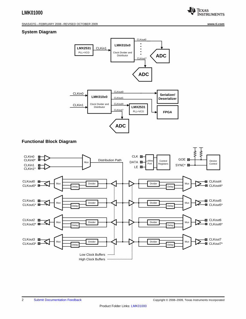
Connection Diagram
Figure 1. 48-Pin LLP Package
Pin Functions
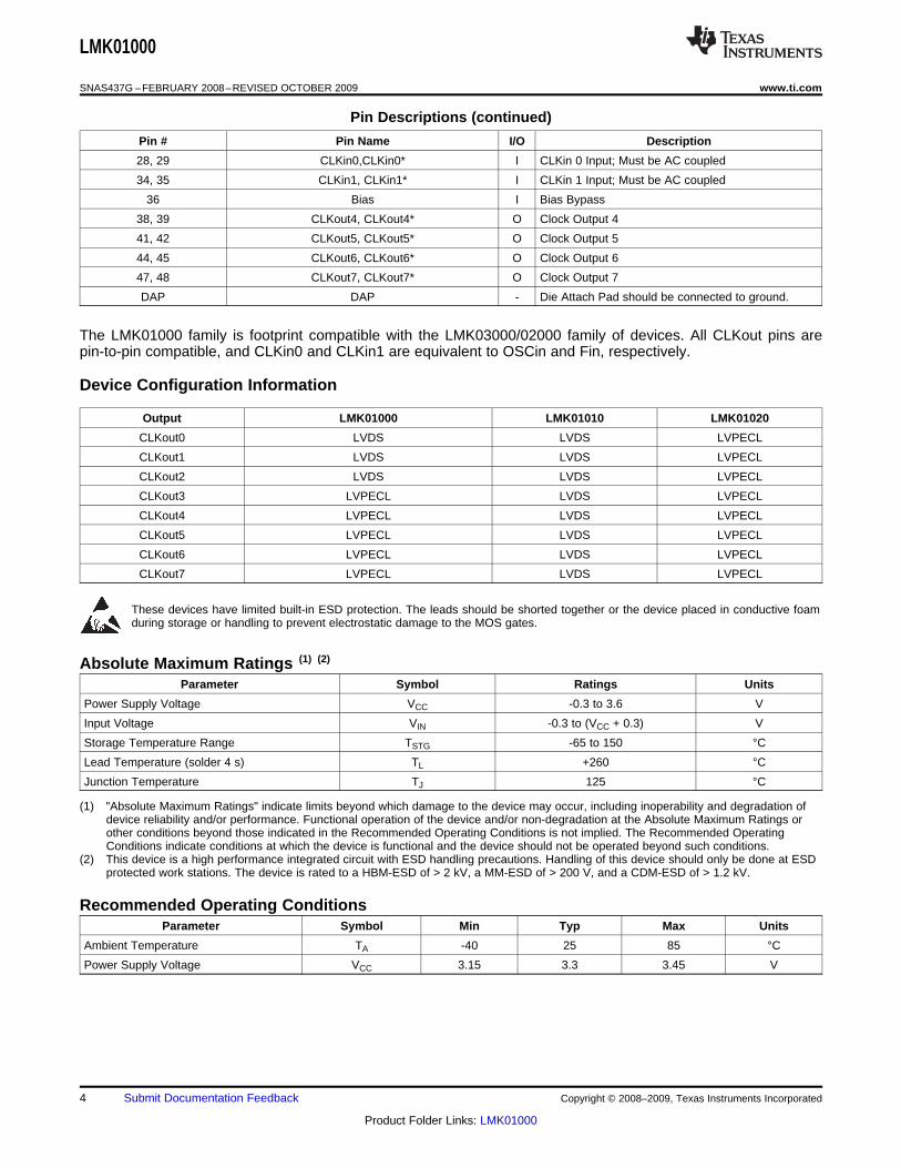
Pin DescriptionsPin # Pin Name I/O Description
1, 25 GND - Ground
2, 7, 9,10, 32 NC - No Connect. Pin is not connected to the die.
3, 8, 13, 16, 19, 22, 26, Vcc1, Vcc2, Vcc3, Vcc4, Vcc5, Vcc6, Vcc7, Vcc8, - Power Supply30, 31, 33, 37, 40, 43, 46 Vcc9, Vcc10, Vcc11, Vcc12, Vcc13, Vcc14
4 CLKuWire I MICROWIRE Clock Input
5 DATAuWire I MICROWIRE Data Input
6 LEuWire I MICROWIRE Latch Enable Input
11 GOE I Global Output Enable
This is an output pin used strictly for test purposesand should be not connected for normal operation.12 Test O However, any load of an impedance of more than 1kΩ is acceptable.
14, 15 CLKout0, CLKout0* O Clock Output 0
17, 18 CLKout1, CLKout1* O Clock Output 1
20, 21 CLKout2, CLKout2* O Clock Output 2
23, 24 CLKout3, CLKout3* O Clock Output 3
27 SYNC* I Global Clock Output Synchronization
Copyright © 2008–2009, Texas Instruments Incorporated Submit Documentation Feedback 3
Product Folder Links: LMK01000
LMK01000
SNAS437G –FEBRUARY 2008–REVISED OCTOBER 2009 www.ti.com
Pin Descriptions (continued)
Pin # Pin Name I/O Description
28, 29 CLKin0,CLKin0* I CLKin 0 Input; Must be AC coupled
34, 35 CLKin1, CLKin1* I CLKin 1 Input; Must be AC coupled
36 Bias I Bias Bypass
38, 39 CLKout4, CLKout4* O Clock Output 4
41, 42 CLKout5, CLKout5* O Clock Output 5
44, 45 CLKout6, CLKout6* O Clock Output 6
47, 48 CLKout7, CLKout7* O Clock Output 7
DAP DAP - Die Attach Pad should be connected to ground.
The LMK01000 family is footprint compatible with the LMK03000/02000 family of devices. All CLKout pins arepin-to-pin compatible, and CLKin0 and CLKin1 are equivalent to OSCin and Fin, respectively.
Device Configuration Information
Output LMK01000 LMK01010 LMK01020
CLKout0 LVDS LVDS LVPECL
CLKout1 LVDS LVDS LVPECL
CLKout2 LVDS LVDS LVPECL
CLKout3 LVPECL LVDS LVPECL
CLKout4 LVPECL LVDS LVPECL
CLKout5 LVPECL LVDS LVPECL
CLKout6 LVPECL LVDS LVPECL
CLKout7 LVPECL LVDS LVPECL
These devices have limited built-in ESD protection. The leads should be shorted together or the device placed in conductive foamduring storage or handling to prevent electrostatic damage to the MOS gates.
Absolute Maximum Ratings (1) (2)
Parameter Symbol Ratings Units
Power Supply Voltage VCC -0.3 to 3.6 V
Input Voltage VIN -0.3 to (VCC + 0.3) V
Storage Temperature Range TSTG -65 to 150 °C
Lead Temperature (solder 4 s) TL +260 °C
Junction Temperature TJ 125 °C
(1) "Absolute Maximum Ratings" indicate limits beyond which damage to the device may occur, including inoperability and degradation ofdevice reliability and/or performance. Functional operation of the device and/or non-degradation at the Absolute Maximum Ratings orother conditions beyond those indicated in the Recommended Operating Conditions is not implied. The Recommended OperatingConditions indicate conditions at which the device is functional and the device should not be operated beyond such conditions.
(2) This device is a high performance integrated circuit with ESD handling precautions. Handling of this device should only be done at ESDprotected work stations. The device is rated to a HBM-ESD of > 2 kV, a MM-ESD of > 200 V, and a CDM-ESD of > 1.2 kV.
Recommended Operating ConditionsParameter Symbol Min Typ Max Units
Ambient Temperature TA -40 25 85 °C
Power Supply Voltage VCC 3.15 3.3 3.45 V
4 Submit Documentation Feedback Copyright © 2008–2009, Texas Instruments Incorporated
Product Folder Links: LMK01000
LMK01000
www.ti.com SNAS437G –FEBRUARY 2008–REVISED OCTOBER 2009
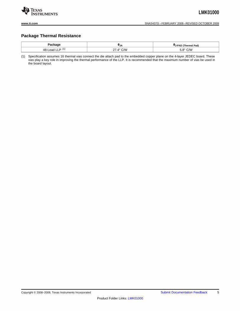
Package Thermal Resistance
Package θJA θJ-PAD (Thermal Pad)
48-Lead LLP (1) 27.4° C/W 5.8° C/W
(1) Specification assumes 16 thermal vias connect the die attach pad to the embedded copper plane on the 4-layer JEDEC board. Thesevias play a key role in improving the thermal performance of the LLP. It is recommended that the maximum number of vias be used inthe board layout.
Copyright © 2008–2009, Texas Instruments Incorporated Submit Documentation Feedback 5
Product Folder Links: LMK01000
LMK01000
SNAS437G –FEBRUARY 2008–REVISED OCTOBER 2009 www.ti.com
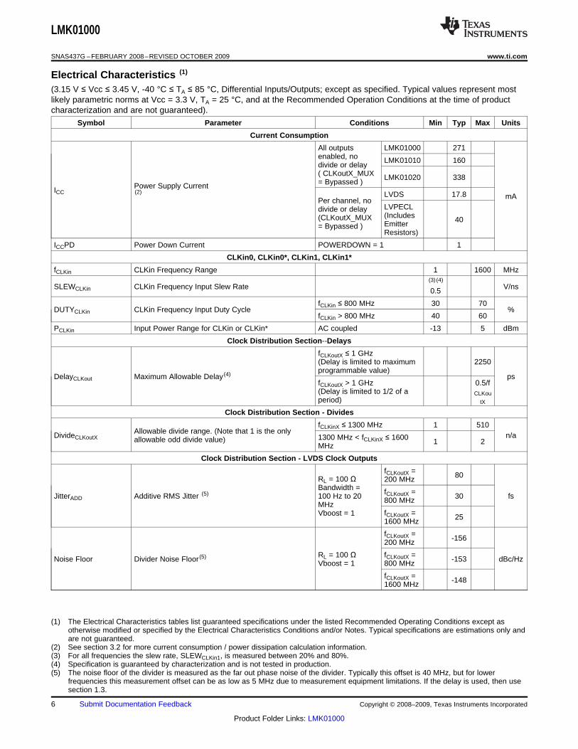
Electrical Characteristics (1)
(3.15 V ≤ Vcc ≤ 3.45 V, -40 °C ≤ TA ≤ 85 °C, Differential Inputs/Outputs; except as specified. Typical values represent mostlikely parametric norms at Vcc = 3.3 V, TA = 25 °C, and at the Recommended Operation Conditions at the time of productcharacterization and are not guaranteed).
Symbol Parameter Conditions Min Typ Max Units
Current Consumption
All outputs LMK01000 271enabled, no LMK01010 160divide or delay( CLKoutX_MUX LMK01020 338= Bypassed )Power Supply CurrentICC (2) LVDS 17.8 mAPer channel, no
LVPECLdivide or delay(Includes(CLKoutX_MUX 40Emitter= Bypassed )Resistors)
ICCPD Power Down Current POWERDOWN = 1 1
CLKin0, CLKin0*, CLKin1, CLKin1*
fCLKin CLKin Frequency Range 1 1600 MHz(3) (4)
SLEWCLKin CLKin Frequency Input Slew Rate V/ns0.5
fCLKin ≤ 800 MHz 30 70DUTYCLKin CLKin Frequency Input Duty Cycle %
fCLKin > 800 MHz 40 60
PCLKin Input Power Range for CLKin or CLKin* AC coupled -13 5 dBm
Clock Distribution Section--Delays
fCLKoutX ≤ 1 GHz(Delay is limited to maximum 2250programmable value)
DelayCLKout Maximum Allowable Delay (4) psfCLKoutX > 1 GHz 0.5/f(Delay is limited to 1/2 of a CLKouperiod) tX
Clock Distribution Section - Divides
fCLKinX ≤ 1300 MHz 1 510Allowable divide range. (Note that 1 is the onlyDivideCLKoutX n/a1300 MHz < fCLKinX ≤ 1600allowable odd divide value) 1 2MHz
Clock Distribution Section - LVDS Clock Outputs
fCLKoutX = 80RL = 100 Ω 200 MHzBandwidth = fCLKoutX =JitterADD Additive RMS Jitter (5) 100 Hz to 20 30 fs800 MHzMHz
fCLKoutX =Vboost = 1 251600 MHz
fCLKoutX = -156200 MHz
RL = 100 Ω fCLKoutX =Noise Floor Divider Noise Floor (5) -153 dBc/HzVboost = 1 800 MHz
fCLKoutX = -1481600 MHz
(1) The Electrical Characteristics tables list guaranteed specifications under the listed Recommended Operating Conditions except asotherwise modified or specified by the Electrical Characteristics Conditions and/or Notes. Typical specifications are estimations only andare not guaranteed.
(2) See section 3.2 for more current consumption / power dissipation calculation information.(3) For all frequencies the slew rate, SLEWCLKin1, is measured between 20% and 80%.(4) Specification is guaranteed by characterization and is not tested in production.(5) The noise floor of the divider is measured as the far out phase noise of the divider. Typically this offset is 40 MHz, but for lower
frequencies this measurement offset can be as low as 5 MHz due to measurement equipment limitations. If the delay is used, then usesection 1.3.
6 Submit Documentation Feedback Copyright © 2008–2009, Texas Instruments Incorporated
Product Folder Links: LMK01000
LMK01000
www.ti.com SNAS437G –FEBRUARY 2008–REVISED OCTOBER 2009
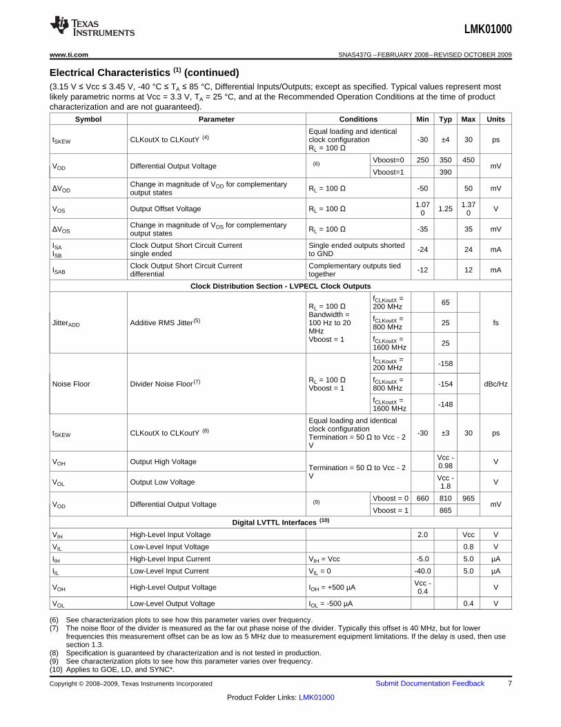
Electrical Characteristics (1) (continued)(3.15 V ≤ Vcc ≤ 3.45 V, -40 °C ≤ TA ≤ 85 °C, Differential Inputs/Outputs; except as specified. Typical values represent mostlikely parametric norms at Vcc = 3.3 V, TA = 25 °C, and at the Recommended Operation Conditions at the time of productcharacterization and are not guaranteed).
Symbol Parameter Conditions Min Typ Max Units
Equal loading and identicaltSKEW CLKoutX to CLKoutY (4) clock configuration -30 ±4 30 ps
RL = 100 ΩVboost=0 250 350 450
VOD Differential Output Voltage (6) mVVboost=1 390
Change in magnitude of VOD for complementaryΔVOD RL = 100 Ω -50 50 mVoutput states
1.07 1.37VOS Output Offset Voltage RL = 100 Ω 1.25 V0 0
Change in magnitude of VOS for complementaryΔVOS RL = 100 Ω -35 35 mVoutput states
ISA Clock Output Short Circuit Current Single ended outputs shorted -24 24 mAISB single ended to GND
Clock Output Short Circuit Current Complementary outputs tiedISAB -12 12 mAdifferential together
Clock Distribution Section - LVPECL Clock Outputs
fCLKoutX = 65RL = 100 Ω 200 MHzBandwidth = fCLKoutX =JitterADD Additive RMS Jitter (5) 100 Hz to 20 25 fs800 MHzMHz
fCLKoutX =Vboost = 1 251600 MHz
fCLKoutX = -158200 MHz
RL = 100 Ω fCLKoutX =Noise Floor Divider Noise Floor (7) -154 dBc/HzVboost = 1 800 MHz
fCLKoutX = -1481600 MHz
Equal loading and identicalclock configurationtSKEW CLKoutX to CLKoutY (8) -30 ±3 30 psTermination = 50 Ω to Vcc - 2V
Vcc -VOH Output High Voltage V0.98Termination = 50 Ω to Vcc - 2V Vcc -VOL Output Low Voltage V1.8
Vboost = 0 660 810 965VOD Differential Output Voltage (9) mV
Vboost = 1 865
Digital LVTTL Interfaces (10)
VIH High-Level Input Voltage 2.0 Vcc V
VIL Low-Level Input Voltage 0.8 V
IIH High-Level Input Current VIH = Vcc -5.0 5.0 µA
IIL Low-Level Input Current VIL = 0 -40.0 5.0 µA
Vcc -VOH High-Level Output Voltage IOH = +500 µA V0.4
VOL Low-Level Output Voltage IOL = -500 µA 0.4 V
(6) See characterization plots to see how this parameter varies over frequency.(7) The noise floor of the divider is measured as the far out phase noise of the divider. Typically this offset is 40 MHz, but for lower
frequencies this measurement offset can be as low as 5 MHz due to measurement equipment limitations. If the delay is used, then usesection 1.3.
(8) Specification is guaranteed by characterization and is not tested in production.(9) See characterization plots to see how this parameter varies over frequency.(10) Applies to GOE, LD, and SYNC*.
Copyright © 2008–2009, Texas Instruments Incorporated Submit Documentation Feedback 7
Product Folder Links: LMK01000
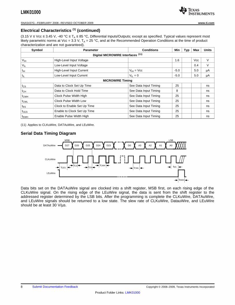
tCEStCS
D27 D26 D25 D24
tCHtCWH
tCWL
D23 D0 A3 A2 A1 A0
MSB LSB
DATAuWire
CLKuWire
LEuWire
tES
tEWH
LMK01000
SNAS437G –FEBRUARY 2008–REVISED OCTOBER 2009 www.ti.com
Electrical Characteristics (1) (continued)(3.15 V ≤ Vcc ≤ 3.45 V, -40 °C ≤ TA ≤ 85 °C, Differential Inputs/Outputs; except as specified. Typical values represent mostlikely parametric norms at Vcc = 3.3 V, TA = 25 °C, and at the Recommended Operation Conditions at the time of productcharacterization and are not guaranteed).
Symbol Parameter Conditions Min Typ Max Units
Digital MICROWIRE Interfaces (11)
VIH High-Level Input Voltage 1.6 Vcc V
VIL Low-Level Input Voltage 0.4 V
IIH High-Level Input Current VIH = Vcc -5.0 5.0 µA
IIL Low-Level Input Current VIL = 0 -5.0 5.0 µA
MICROWIRE Timing
tCS Data to Clock Set Up Time See Data Input Timing 25 ns
tCH Data to Clock Hold Time See Data Input Timing 8 ns
tCWH Clock Pulse Width High See Data Input Timing 25 ns
tCWL Clock Pulse Width Low See Data Input Timing 25 ns
tES Clock to Enable Set Up Time See Data Input Timing 25 ns
tCES Enable to Clock Set Up Time See Data Input Timing 25 ns
tEWH Enable Pulse Width High See Data Input Timing 25 ns
(11) Applies to CLKuWire, DATAuWire, and LEuWire.
Serial Data Timing Diagram
Data bits set on the DATAuWire signal are clocked into a shift register, MSB first, on each rising edge of theCLKuWire signal. On the rising edge of the LEuWire signal, the data is sent from the shift register to theaddressed register determined by the LSB bits. After the programming is complete the CLKuWire, DATAuWire,and LEuWire signals should be returned to a low state. The slew rate of CLKuWire, DatauWire, and LEuWireshould be at least 30 V/µs.
8 Submit Documentation Feedback Copyright © 2008–2009, Texas Instruments Incorporated
Product Folder Links: LMK01000
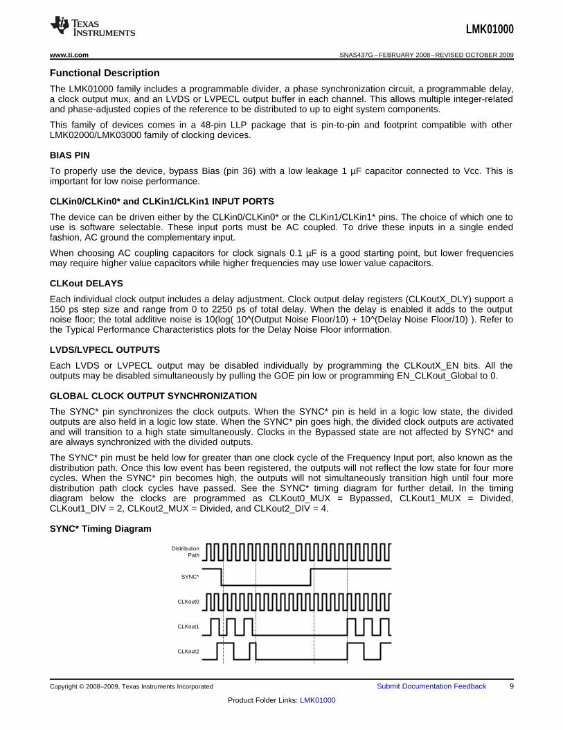
DistributionPath
SYNC*
CLKout0
CLKout1
CLKout2
LMK01000
www.ti.com SNAS437G –FEBRUARY 2008–REVISED OCTOBER 2009
Functional Description
The LMK01000 family includes a programmable divider, a phase synchronization circuit, a programmable delay,a clock output mux, and an LVDS or LVPECL output buffer in each channel. This allows multiple integer-relatedand phase-adjusted copies of the reference to be distributed to up to eight system components.
This family of devices comes in a 48-pin LLP package that is pin-to-pin and footprint compatible with otherLMK02000/LMK03000 family of clocking devices.
BIAS PIN
To properly use the device, bypass Bias (pin 36) with a low leakage 1 µF capacitor connected to Vcc. This isimportant for low noise performance.
CLKin0/CLKin0* and CLKin1/CLKin1 INPUT PORTS
The device can be driven either by the CLKin0/CLKin0* or the CLKin1/CLKin1* pins. The choice of which one touse is software selectable. These input ports must be AC coupled. To drive these inputs in a single endedfashion, AC ground the complementary input.
When choosing AC coupling capacitors for clock signals 0.1 µF is a good starting point, but lower frequenciesmay require higher value capacitors while higher frequencies may use lower value capacitors.
CLKout DELAYS
Each individual clock output includes a delay adjustment. Clock output delay registers (CLKoutX_DLY) support a150 ps step size and range from 0 to 2250 ps of total delay. When the delay is enabled it adds to the outputnoise floor; the total additive noise is 10(log( 10^(Output Noise Floor/10) + 10^(Delay Noise Floor/10) ). Refer tothe Typical Performance Characteristics plots for the Delay Noise Floor information.
LVDS/LVPECL OUTPUTS
Each LVDS or LVPECL output may be disabled individually by programming the CLKoutX_EN bits. All theoutputs may be disabled simultaneously by pulling the GOE pin low or programming EN_CLKout_Global to 0.
GLOBAL CLOCK OUTPUT SYNCHRONIZATION
The SYNC* pin synchronizes the clock outputs. When the SYNC* pin is held in a logic low state, the dividedoutputs are also held in a logic low state. When the SYNC* pin goes high, the divided clock outputs are activatedand will transition to a high state simultaneously. Clocks in the Bypassed state are not affected by SYNC* andare always synchronized with the divided outputs.
The SYNC* pin must be held low for greater than one clock cycle of the Frequency Input port, also known as thedistribution path. Once this low event has been registered, the outputs will not reflect the low state for four morecycles. When the SYNC* pin becomes high, the outputs will not simultaneously transition high until four moredistribution path clock cycles have passed. See the SYNC* timing diagram for further detail. In the timingdiagram below the clocks are programmed as CLKout0_MUX = Bypassed, CLKout1_MUX = Divided,CLKout1_DIV = 2, CLKout2_MUX = Divided, and CLKout2_DIV = 4.
SYNC* Timing Diagram
Copyright © 2008–2009, Texas Instruments Incorporated Submit Documentation Feedback 9
Product Folder Links: LMK01000
LMK01000
SNAS437G –FEBRUARY 2008–REVISED OCTOBER 2009 www.ti.com
The SYNC* pin provides an internal pull-up resistor as shown on the functional block diagram. If the SYNC* pinis not terminated externally the clock outputs will operate normally. If the SYNC* function is not used, clockoutput synchronization is not guaranteed.
CONNECTION TO LVDS OUTPUTS
LMK01000 and LMK01010 LVDS outputs can be connected in AC or DC coupling configurations; however, in DCcoupling configuration, proper conditions must be presented by the LVDS receiver. To ensure such conditions,we recommend the usage of LVDS receivers without fail-safe or internal input bias such as NationalSemiconductor's DS90LV110T. The LMK01000 family LVDS drivers provide the adequate DC bias for the LVDSreceiver. We recommend AC coupling when using LVDS receivers with fail-safe or internal input bias.
CLKout OUTPUT STATES
Each clock output may be individually enabled with the CLKoutX_EN bits. Each individual output enable controlbit is gated with the Global Output Enable input pin (GOE) and the Global Output Enable bit(EN_CLKout_Global).
All clock outputs can be disabled simultaneously if the GOE pin is pulled low by an external signal orEN_CLKout_Global is set to 0.
CLKoutX EN_CLKout GOE pin Clock X Output State_EN bit _Global bit
1 1 Low Low
Don't care 0 Don't care Off
0 Don't care Don't care Off
1 1 High / No Connect Enabled
When an LVDS output is in the Off state, the outputs are at a voltage of approximately 1.5 volts. When anLVPECL output is in the Off state, the outputs are at a voltage of approximately 1 volt.
GLOBAL OUTPUT ENABLE
The GOE pin provides an internal pull-up resistor. If it is not terminated externally, the clock output states aredetermined by the Clock Output Enable bits (CLKoutX_EN) and the EN_CLKout_Global bit.
POWER-ON-RESET
When supply voltage to the device increases monotonically from ground to Vcc, the power-on-reset circuit setsall registers to their default values, which are specified in the General Programming Information section. Voltageshould be applied to all Vcc pins simultaneously.
General Programming Information
The LMK01000 family device is programmed using several 32-bit registers. The registers consist of a data fieldand an address field. The last 4 register bits, ADDR[3:0] form the address field. The remaining 28 bits form thedata field DATA[27:0].
During programming, LEuWire is low and serial data is clocked in on the rising edge of clock (MSB first). WhenLEuWire goes high, data is transferred to the register bank selected by the address field. Only registers R0 to R7and R14 need to be programmed for proper device operation.
It is required to program register R14.
RECOMMENDED PROGRAMMING SEQUENCE
The recommended programming sequence involves programming R0 with the reset bit set (RESET = 1) toensure the device is in a default state. It is not necessary to program R0 again, but if R0 is programmed again,the reset bit is programmed clear (RESET = 0). An example programming sequence is shown below.• Program R0 with the reset bit set (RESET = 1). This ensures the device is in a default state. When the reset
bit is set in R0, the other R0 bits are ignored.– If R0 is programmed again, the reset bit is programmed clear (RESET = 0).
10 Submit Documentation Feedback Copyright © 2008–2009, Texas Instruments Incorporated
Product Folder Links: LMK01000
LMK01000
www.ti.com SNAS437G –FEBRUARY 2008–REVISED OCTOBER 2009
• Program R0 to R7 as necessary with desired clocks with appropriate enable, mux, divider, and delay settings.• Program R14 with global clock output bit, power down setting.
– R14 must be programmed in accordance with the register map as shown in the register map (See Section2.2).
Table 1. Register MapRegis 31 30 29 28 27 26 25 24 23 22 21 20 19 18 17 16 15 14 13 12 11 10 9 8 7 6 5 4 3 2 1 0ter
Data [27:0] A3 A2 A1 A0
CLRE CLKout0 Ko
CLKout0_DIV CLKout0_DLYR0 SE 0 0 0 0 0 0 0 0 0 0 0 0 _MUX ut0 0 0 0 0
[7:0] [3:0]T [1:0] _E
N
CLCLKout1 Ko
CLKout1_DIV CLKout1_DLYR1 0 0 0 0 0 0 0 0 0 0 0 0 0 _MUX ut1 0 0 0 1
[7:0] [3:0][1:0] _E
N
CLCLKout2 Ko
CLKout2_DIV CLKout2_DLYR2 0 0 0 0 0 0 0 0 0 0 0 0 0 _MUX ut2 0 0 1 0
[7:0] [3:0][1:0] _E
N
CLCLKout3 Ko
CLKout3_DIV CLKout3_DLYR3 0 0 0 0 0 0 0 0 0 0 0 0 0 _MUX ut3 0 0 1 1
[7:0] [3:0][1:0] _E
N
CLCLKout4 Ko
CLKout4_DIV CLKout4_DLYR4 0 0 0 0 0 0 0 0 0 0 0 0 0 _MUX ut4 0 1 0 0
[7:0] [3:0][1:0] _E
N
CLCLKout5 Ko
CLKout5_DIV CLKout5_DLYR5 0 0 0 0 0 0 0 0 0 0 0 0 0 _MUX ut5 0 1 0 1
[7:0] [3:0][1:0] _E
N
CLCLKout6 Ko
CLKout6_DIV CLKout6_DLYR6 0 0 0 0 0 0 0 0 0 0 0 0 0 _MUX ut6 0 1 1 0
[7:0] [3:0][1:0] _E
N
CLCLKout7 Ko
CLKout7_DIV CLKout7_DLYR7 0 0 0 0 0 0 0 0 0 0 0 0 0 _MUX ut7 0 1 1 1
[7:0] [3:0][1:0] _E
N
VbR9 0 0 0 0 0 0 0 0 0 0 0 0 0 0 1 o 0 0 1 0 1 0 1 0 0 0 0 0 1 0 0 1
ost
ENCL PO
_CKin W
LKR1 _S ER
0 1 0 out 0 0 0 0 0 0 0 0 0 0 0 0 0 0 0 0 0 0 0 0 0 0 1 1 1 04 EL DO
_GEC W
lobT N
al
REGISTER R0 to R7
Registers R0 through R7 control the eight clock outputs. Register R0 controls CLKout0, Register R1 controlsCLKout1, and so on. There is one additional bit in register R0 called RESET. Aside from this, the functions ofthese bits are identical. The X in CLKoutX_MUX, CLKoutX_DIV, CLKoutX_DLY, and CLKoutX_EN denote theactual clock output which may be from 0 to 7.
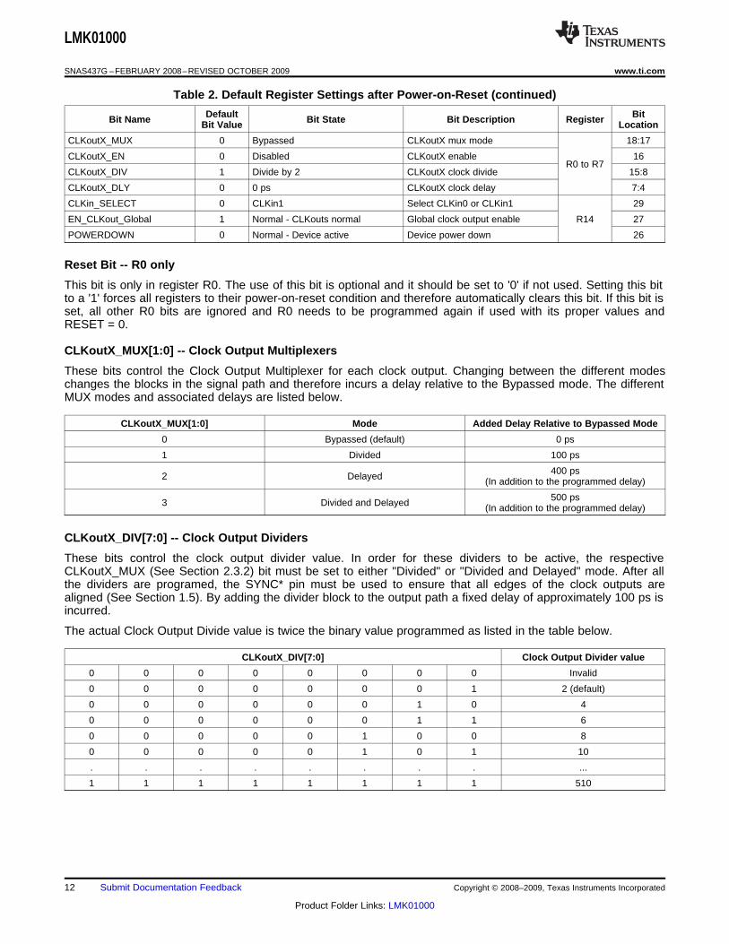
Table 2. Default Register Settings after Power-on-Reset
Default BitBit Name Bit State Bit Description RegisterBit Value Location
RESET 0 No reset, normal operation Reset to power on defaults R0 31
Copyright © 2008–2009, Texas Instruments Incorporated Submit Documentation Feedback 11
Product Folder Links: LMK01000
LMK01000
SNAS437G –FEBRUARY 2008–REVISED OCTOBER 2009 www.ti.com
Table 2. Default Register Settings after Power-on-Reset (continued)
Default BitBit Name Bit State Bit Description RegisterBit Value Location
CLKoutX_MUX 0 Bypassed CLKoutX mux mode 18:17
CLKoutX_EN 0 Disabled CLKoutX enable 16R0 to R7
CLKoutX_DIV 1 Divide by 2 CLKoutX clock divide 15:8
CLKoutX_DLY 0 0 ps CLKoutX clock delay 7:4
CLKin_SELECT 0 CLKin1 Select CLKin0 or CLKin1 29
EN_CLKout_Global 1 Normal - CLKouts normal Global clock output enable R14 27
POWERDOWN 0 Normal - Device active Device power down 26
Reset Bit -- R0 only
This bit is only in register R0. The use of this bit is optional and it should be set to '0' if not used. Setting this bitto a '1' forces all registers to their power-on-reset condition and therefore automatically clears this bit. If this bit isset, all other R0 bits are ignored and R0 needs to be programmed again if used with its proper values andRESET = 0.
CLKoutX_MUX[1:0] -- Clock Output Multiplexers
These bits control the Clock Output Multiplexer for each clock output. Changing between the different modeschanges the blocks in the signal path and therefore incurs a delay relative to the Bypassed mode. The differentMUX modes and associated delays are listed below.
CLKoutX_MUX[1:0] Mode Added Delay Relative to Bypassed Mode
0 Bypassed (default) 0 ps
1 Divided 100 ps
400 ps2 Delayed (In addition to the programmed delay)
500 ps3 Divided and Delayed (In addition to the programmed delay)
CLKoutX_DIV[7:0] -- Clock Output Dividers
These bits control the clock output divider value. In order for these dividers to be active, the respectiveCLKoutX_MUX (See Section 2.3.2) bit must be set to either "Divided" or "Divided and Delayed" mode. After allthe dividers are programed, the SYNC* pin must be used to ensure that all edges of the clock outputs arealigned (See Section 1.5). By adding the divider block to the output path a fixed delay of approximately 100 ps isincurred.
The actual Clock Output Divide value is twice the binary value programmed as listed in the table below.
CLKoutX_DIV[7:0] Clock Output Divider value
0 0 0 0 0 0 0 0 Invalid
0 0 0 0 0 0 0 1 2 (default)
0 0 0 0 0 0 1 0 4
0 0 0 0 0 0 1 1 6
0 0 0 0 0 1 0 0 8
0 0 0 0 0 1 0 1 10
. . . . . . . . ...
1 1 1 1 1 1 1 1 510
12 Submit Documentation Feedback Copyright © 2008–2009, Texas Instruments Incorporated
Product Folder Links: LMK01000
LMK01000
www.ti.com SNAS437G –FEBRUARY 2008–REVISED OCTOBER 2009
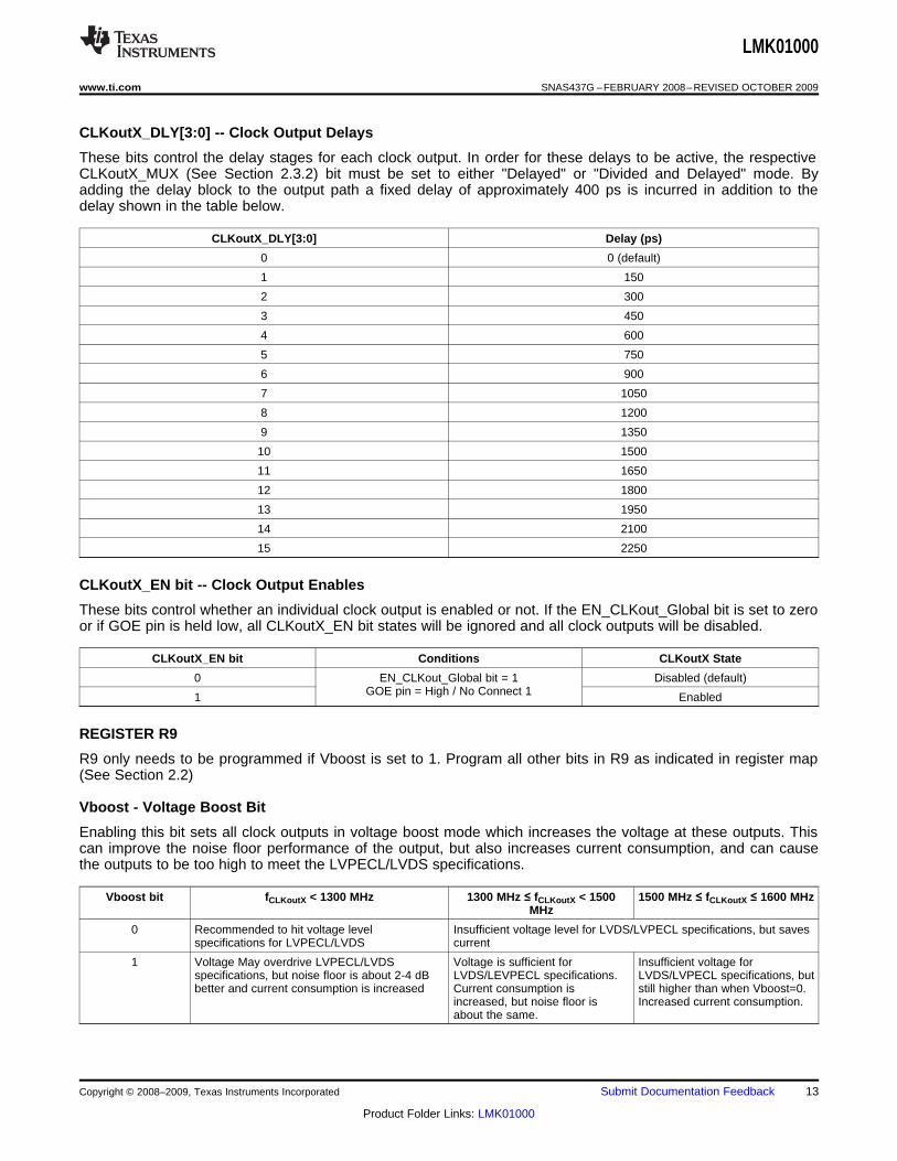
CLKoutX_DLY[3:0] -- Clock Output Delays
These bits control the delay stages for each clock output. In order for these delays to be active, the respectiveCLKoutX_MUX (See Section 2.3.2) bit must be set to either "Delayed" or "Divided and Delayed" mode. Byadding the delay block to the output path a fixed delay of approximately 400 ps is incurred in addition to thedelay shown in the table below.
CLKoutX_DLY[3:0] Delay (ps)
0 0 (default)
1 150
2 300
3 450
4 600
5 750
6 900
7 1050
8 1200
9 1350
10 1500
11 1650
12 1800
13 1950
14 2100
15 2250
CLKoutX_EN bit -- Clock Output Enables
These bits control whether an individual clock output is enabled or not. If the EN_CLKout_Global bit is set to zeroor if GOE pin is held low, all CLKoutX_EN bit states will be ignored and all clock outputs will be disabled.
CLKoutX_EN bit Conditions CLKoutX State
0 EN_CLKout_Global bit = 1 Disabled (default)GOE pin = High / No Connect 11 Enabled
REGISTER R9
R9 only needs to be programmed if Vboost is set to 1. Program all other bits in R9 as indicated in register map(See Section 2.2)
Vboost - Voltage Boost Bit
Enabling this bit sets all clock outputs in voltage boost mode which increases the voltage at these outputs. Thiscan improve the noise floor performance of the output, but also increases current consumption, and can causethe outputs to be too high to meet the LVPECL/LVDS specifications.
Vboost bit fCLKoutX < 1300 MHz 1300 MHz ≤ fCLKoutX < 1500 1500 MHz ≤ fCLKoutX ≤ 1600 MHzMHz
0 Recommended to hit voltage level Insufficient voltage level for LVDS/LVPECL specifications, but savesspecifications for LVPECL/LVDS current
1 Voltage May overdrive LVPECL/LVDS Voltage is sufficient for Insufficient voltage forspecifications, but noise floor is about 2-4 dB LVDS/LEVPECL specifications. LVDS/LVPECL specifications, butbetter and current consumption is increased Current consumption is still higher than when Vboost=0.
increased, but noise floor is Increased current consumption.about the same.
Copyright © 2008–2009, Texas Instruments Incorporated Submit Documentation Feedback 13
Product Folder Links: LMK01000
OS
Cin
LMX2531100 pF
Fout CLKin1
DA
TA
CLK
LE
Microcontroller
CLK
DATA
CLKuWire
DATAuWire
LE
LEuWire
LMK010X0
100
nF
100
nF
OS
Cin
*
LEuW
ire
Tes
t
Tes
t
Vre
fVC
O
Vre
gBU
F
Vre
gDIG
3.3 :
4.7 P
F
10 n
F
0.22
:47
0 nF
0.22
:47
0 nF
10 n
F
10 n
F
Vre
gPLL
1
Vre
gPLL
2
CLKin1*100 pF
3.0 V
Vre
gVC
O
Vcc
VC
O
Vcc
DIG
Vcc
BU
F
Vcc
PLL
Vtu
neC
Pou
t
C1_
LF
C2_
LFR
2_LF
3.3 V
Vcc
1
...
Vcc
2
...
Vcc
13V
cc14
CE
Bia
s
SY
NC
*G
OE
CLK
out0
CLK
out0
*
...
CLK
out7
CLK
out7
*
To Other Devices
100
nF
LMK01000
SNAS437G –FEBRUARY 2008–REVISED OCTOBER 2009 www.ti.com
REGISTER R14
The LMK01000 family requires register R14 to be programmed as shown in the register map (See Section 2.2).
POWERDOWN Bit -- Device Power Down
This bit can power down the device. Enabling this bit powers down the entire device and all blocks, regardless ofthe state of any of the other bits or pins.
POWERDOWN bit Mode
0 Normal Operation (default)
1 Entire Device Powered Down
EN_CLKout_Global Bit -- Global Clock Output Enable
This bit overrides the individual CLKoutX_EN bits. When thisbit is set to 0, all clock outputs are disabled,regardless of thestate of any of the other bits or pins.
EN_CLKout_Global bit Clock Outputs
0 All Off
1 Normal Operation (default)
CLKin_SELECT Bit -- Device CLKin Select
This bit determines which CLKin pin is used.
CLKin bit Mode
0 CLKin1 (default)
1 CLKin0
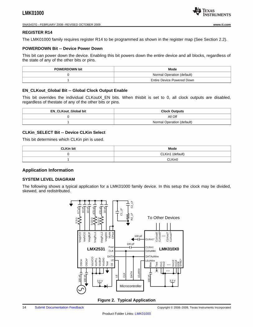
Application Information
SYSTEM LEVEL DIAGRAM
The following shows a typical application for a LMK01000 family device. In this setup the clock may be divided,skewed, and redistributed.
Figure 2. Typical Application
14 Submit Documentation Feedback Copyright © 2008–2009, Texas Instruments Incorporated
Product Folder Links: LMK01000
LMK01000
www.ti.com SNAS437G –FEBRUARY 2008–REVISED OCTOBER 2009
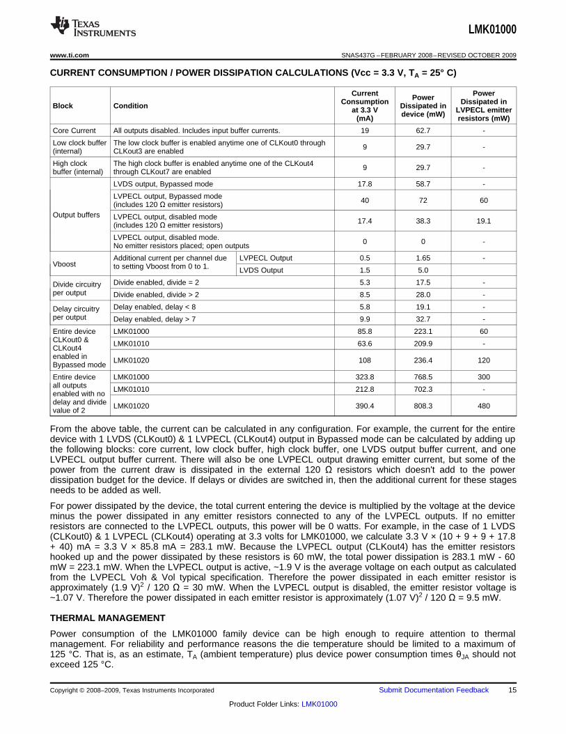
CURRENT CONSUMPTION / POWER DISSIPATION CALCULATIONS (Vcc = 3.3 V, TA = 25° C)
Current PowerPowerConsumption Dissipated inBlock Condition Dissipated inat 3.3 V LVPECL emitterdevice (mW)(mA) resistors (mW)
Core Current All outputs disabled. Includes input buffer currents. 19 62.7 -
Low clock buffer The low clock buffer is enabled anytime one of CLKout0 through 9 29.7 -(internal) CLKout3 are enabled
High clock The high clock buffer is enabled anytime one of the CLKout4 9 29.7 -buffer (internal) through CLKout7 are enabled
LVDS output, Bypassed mode 17.8 58.7 -
LVPECL output, Bypassed mode 40 72 60(includes 120 Ω emitter resistors)Output buffers LVPECL output, disabled mode 17.4 38.3 19.1(includes 120 Ω emitter resistors)
LVPECL output, disabled mode. 0 0 -No emitter resistors placed; open outputs
Additional current per channel due LVPECL Output 0.5 1.65 -Vboost to setting Vboost from 0 to 1. LVDS Output 1.5 5.0
Divide enabled, divide = 2 5.3 17.5 -Divide circuitryper output Divide enabled, divide > 2 8.5 28.0 -
Delay enabled, delay < 8 5.8 19.1 -Delay circuitryper output Delay enabled, delay > 7 9.9 32.7 -
Entire device LMK01000 85.8 223.1 60CLKout0 & LMK01010 63.6 209.9 -CLKout4enabled in LMK01020 108 236.4 120Bypassed mode
Entire device LMK01000 323.8 768.5 300all outputs LMK01010 212.8 702.3 -enabled with nodelay and divide LMK01020 390.4 808.3 480value of 2
From the above table, the current can be calculated in any configuration. For example, the current for the entiredevice with 1 LVDS (CLKout0) & 1 LVPECL (CLKout4) output in Bypassed mode can be calculated by adding upthe following blocks: core current, low clock buffer, high clock buffer, one LVDS output buffer current, and oneLVPECL output buffer current. There will also be one LVPECL output drawing emitter current, but some of thepower from the current draw is dissipated in the external 120 Ω resistors which doesn't add to the powerdissipation budget for the device. If delays or divides are switched in, then the additional current for these stagesneeds to be added as well.
For power dissipated by the device, the total current entering the device is multiplied by the voltage at the deviceminus the power dissipated in any emitter resistors connected to any of the LVPECL outputs. If no emitterresistors are connected to the LVPECL outputs, this power will be 0 watts. For example, in the case of 1 LVDS(CLKout0) & 1 LVPECL (CLKout4) operating at 3.3 volts for LMK01000, we calculate 3.3 V × (10 + 9 + 9 + 17.8+ 40) mA = 3.3 V × 85.8 mA = 283.1 mW. Because the LVPECL output (CLKout4) has the emitter resistorshooked up and the power dissipated by these resistors is 60 mW, the total power dissipation is 283.1 mW - 60mW = 223.1 mW. When the LVPECL output is active, ~1.9 V is the average voltage on each output as calculatedfrom the LVPECL Voh & Vol typical specification. Therefore the power dissipated in each emitter resistor isapproximately (1.9 V)2 / 120 Ω = 30 mW. When the LVPECL output is disabled, the emitter resistor voltage is~1.07 V. Therefore the power dissipated in each emitter resistor is approximately (1.07 V)2 / 120 Ω = 9.5 mW.
THERMAL MANAGEMENT
Power consumption of the LMK01000 family device can be high enough to require attention to thermalmanagement. For reliability and performance reasons the die temperature should be limited to a maximum of125 °C. That is, as an estimate, TA (ambient temperature) plus device power consumption times θJA should notexceed 125 °C.
Copyright © 2008–2009, Texas Instruments Incorporated Submit Documentation Feedback 15
Product Folder Links: LMK01000
0.33 mm, typ
1.2 mm, typ
5.0 mm, min
LMK01000
SNAS437G –FEBRUARY 2008–REVISED OCTOBER 2009 www.ti.com
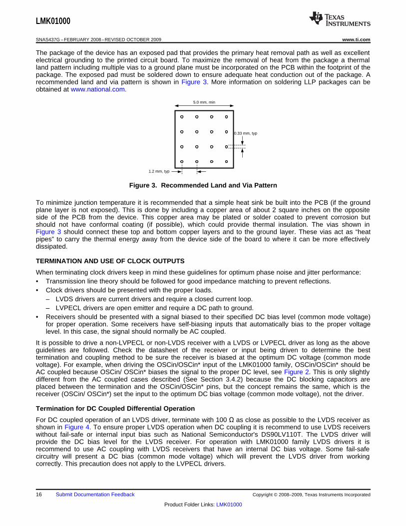
The package of the device has an exposed pad that provides the primary heat removal path as well as excellentelectrical grounding to the printed circuit board. To maximize the removal of heat from the package a thermalland pattern including multiple vias to a ground plane must be incorporated on the PCB within the footprint of thepackage. The exposed pad must be soldered down to ensure adequate heat conduction out of the package. Arecommended land and via pattern is shown in Figure 3. More information on soldering LLP packages can beobtained at www.national.com.
Figure 3. Recommended Land and Via Pattern
To minimize junction temperature it is recommended that a simple heat sink be built into the PCB (if the groundplane layer is not exposed). This is done by including a copper area of about 2 square inches on the oppositeside of the PCB from the device. This copper area may be plated or solder coated to prevent corrosion butshould not have conformal coating (if possible), which could provide thermal insulation. The vias shown inFigure 3 should connect these top and bottom copper layers and to the ground layer. These vias act as “heatpipes” to carry the thermal energy away from the device side of the board to where it can be more effectivelydissipated.
TERMINATION AND USE OF CLOCK OUTPUTS
When terminating clock drivers keep in mind these guidelines for optimum phase noise and jitter performance:• Transmission line theory should be followed for good impedance matching to prevent reflections.• Clock drivers should be presented with the proper loads.
– LVDS drivers are current drivers and require a closed current loop.– LVPECL drivers are open emitter and require a DC path to ground.
• Receivers should be presented with a signal biased to their specified DC bias level (common mode voltage)for proper operation. Some receivers have self-biasing inputs that automatically bias to the proper voltagelevel. In this case, the signal should normally be AC coupled.
It is possible to drive a non-LVPECL or non-LVDS receiver with a LVDS or LVPECL driver as long as the aboveguidelines are followed. Check the datasheet of the receiver or input being driven to determine the besttermination and coupling method to be sure the receiver is biased at the optimum DC voltage (common modevoltage). For example, when driving the OSCin/OSCin* input of the LMK01000 family, OSCin/OSCin* should beAC coupled because OSCin/ OSCin* biases the signal to the proper DC level, see Figure 2. This is only slightlydifferent from the AC coupled cases described (See Section 3.4.2) because the DC blocking capacitors areplaced between the termination and the OSCin/OSCin* pins, but the concept remains the same, which is thereceiver (OSCin/ OSCin*) set the input to the optimum DC bias voltage (common mode voltage), not the driver.
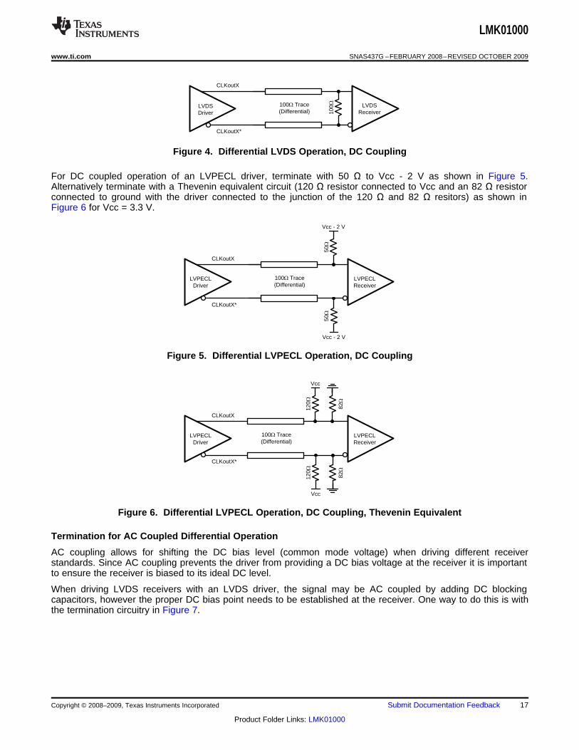
Termination for DC Coupled Differential Operation
For DC coupled operation of an LVDS driver, terminate with 100 Ω as close as possible to the LVDS receiver asshown in Figure 4. To ensure proper LVDS operation when DC coupling it is recommend to use LVDS receiverswithout fail-safe or internal input bias such as National Semiconductor's DS90LV110T. The LVDS driver willprovide the DC bias level for the LVDS receiver. For operation with LMK01000 family LVDS drivers it isrecommend to use AC coupling with LVDS receivers that have an internal DC bias voltage. Some fail-safecircuitry will present a DC bias (common mode voltage) which will prevent the LVDS driver from workingcorrectly. This precaution does not apply to the LVPECL drivers.
16 Submit Documentation Feedback Copyright © 2008–2009, Texas Instruments Incorporated
Product Folder Links: LMK01000
CLKoutX
CLKoutX*
LVPECL Receiver
120:
100:�Trace(Differential)
120:
Vcc
Vcc
LVPECL Driver
82:
82:
CLKoutX
CLKoutX*
LVPECL Receiver
50:
100:�Trace(Differential)
50:
Vcc - 2 V
Vcc - 2 V
LVPECL Driver
CLKoutX
CLKoutX*
LVDS Receiver10
0:100:�Trace(Differential)
LVDSDriver
LMK01000
www.ti.com SNAS437G –FEBRUARY 2008–REVISED OCTOBER 2009
Figure 4. Differential LVDS Operation, DC Coupling
For DC coupled operation of an LVPECL driver, terminate with 50 Ω to Vcc - 2 V as shown in Figure 5.Alternatively terminate with a Thevenin equivalent circuit (120 Ω resistor connected to Vcc and an 82 Ω resistorconnected to ground with the driver connected to the junction of the 120 Ω and 82 Ω resitors) as shown inFigure 6 for Vcc = 3.3 V.
Figure 5. Differential LVPECL Operation, DC Coupling
Figure 6. Differential LVPECL Operation, DC Coupling, Thevenin Equivalent
Termination for AC Coupled Differential Operation
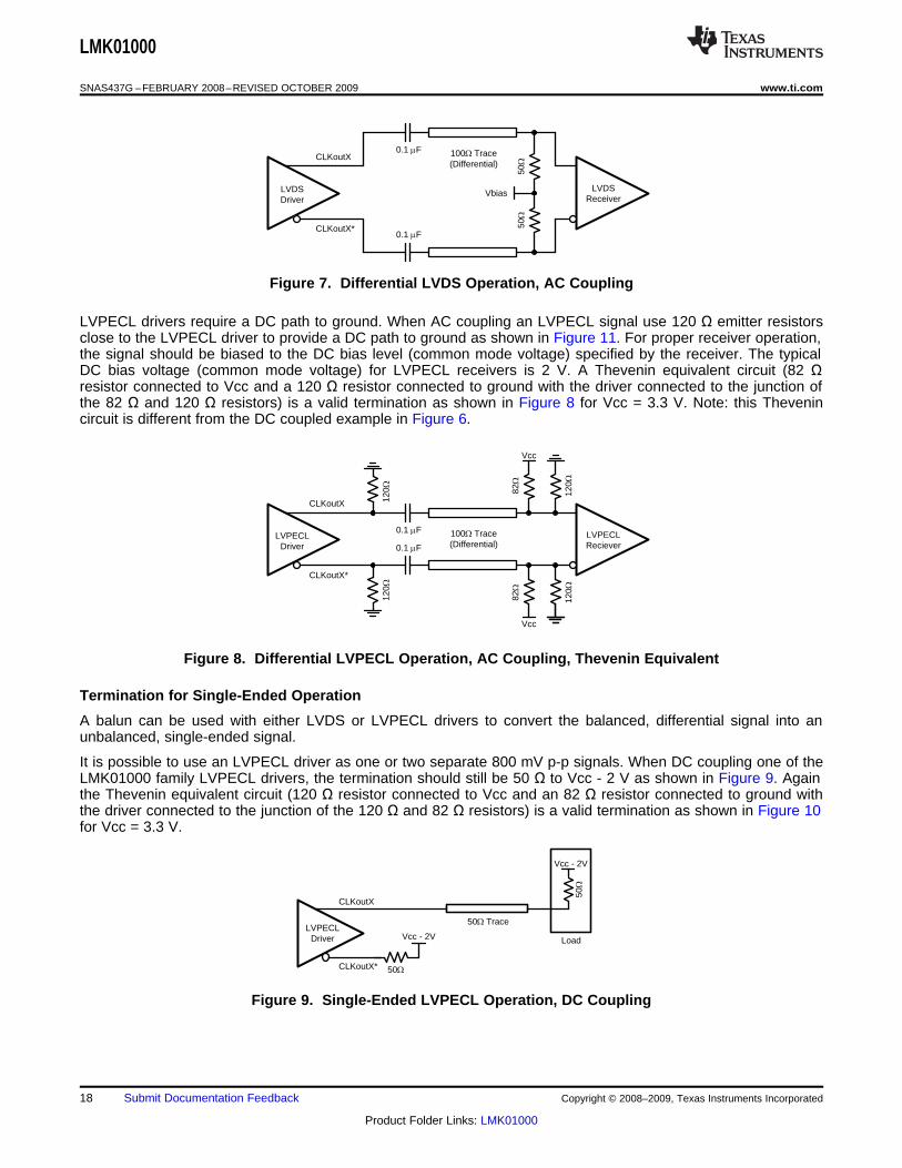
AC coupling allows for shifting the DC bias level (common mode voltage) when driving different receiverstandards. Since AC coupling prevents the driver from providing a DC bias voltage at the receiver it is importantto ensure the receiver is biased to its ideal DC level.
When driving LVDS receivers with an LVDS driver, the signal may be AC coupled by adding DC blockingcapacitors, however the proper DC bias point needs to be established at the receiver. One way to do this is withthe termination circuitry in Figure 7.
Copyright © 2008–2009, Texas Instruments Incorporated Submit Documentation Feedback 17
Product Folder Links: LMK01000
CLKoutX
CLKoutX* 50:
50:�Trace
50:
Load
Vcc - 2V
Vcc - 2VLVPECL
Driver
CLKoutX
CLKoutX*
120:
120:
0.1 PF
0.1 PF
LVPECL Reciever
100:�Trace(Differential)
LVPECLDriver
82:
120:
Vcc
82:
120:
Vcc
CLKoutX
CLKoutX*
0.1 PF
0.1 PF
LVDS Receiver
50:
100:�Trace(Differential)
LVDSDriver
50:
Vbias
LMK01000
SNAS437G –FEBRUARY 2008–REVISED OCTOBER 2009 www.ti.com
Figure 7. Differential LVDS Operation, AC Coupling
LVPECL drivers require a DC path to ground. When AC coupling an LVPECL signal use 120 Ω emitter resistorsclose to the LVPECL driver to provide a DC path to ground as shown in Figure 11. For proper receiver operation,the signal should be biased to the DC bias level (common mode voltage) specified by the receiver. The typicalDC bias voltage (common mode voltage) for LVPECL receivers is 2 V. A Thevenin equivalent circuit (82 Ωresistor connected to Vcc and a 120 Ω resistor connected to ground with the driver connected to the junction ofthe 82 Ω and 120 Ω resistors) is a valid termination as shown in Figure 8 for Vcc = 3.3 V. Note: this Thevenincircuit is different from the DC coupled example in Figure 6.
Figure 8. Differential LVPECL Operation, AC Coupling, Thevenin Equivalent
Termination for Single-Ended Operation
A balun can be used with either LVDS or LVPECL drivers to convert the balanced, differential signal into anunbalanced, single-ended signal.
It is possible to use an LVPECL driver as one or two separate 800 mV p-p signals. When DC coupling one of theLMK01000 family LVPECL drivers, the termination should still be 50 Ω to Vcc - 2 V as shown in Figure 9. Againthe Thevenin equivalent circuit (120 Ω resistor connected to Vcc and an 82 Ω resistor connected to ground withthe driver connected to the junction of the 120 Ω and 82 Ω resistors) is a valid termination as shown in Figure 10for Vcc = 3.3 V.
Figure 9. Single-Ended LVPECL Operation, DC Coupling
18 Submit Documentation Feedback Copyright © 2008–2009, Texas Instruments Incorporated
Product Folder Links: LMK01000
0.1 PF
0.1 PF
50:�Trace
50: LMK
InputClock Source
CLKoutX
CLKoutX*
120:
120:
0.1 PF
0.1 PF
50:�Trace50:
Load50:
LVPECLDriver
CLKoutX
CLKoutX*
82:
50:�Trace
120:
Load
Vcc
82:
120:
VccLVPECL
Driver
LMK01000
www.ti.com SNAS437G –FEBRUARY 2008–REVISED OCTOBER 2009
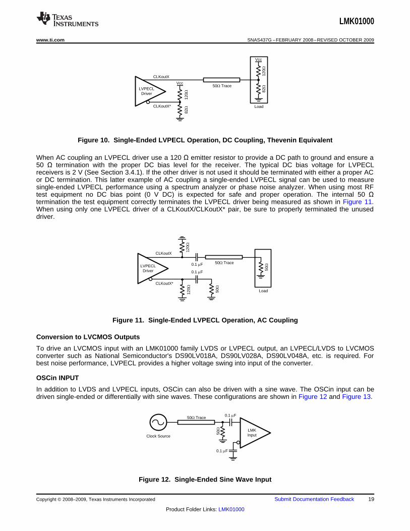
Figure 10. Single-Ended LVPECL Operation, DC Coupling, Thevenin Equivalent
When AC coupling an LVPECL driver use a 120 Ω emitter resistor to provide a DC path to ground and ensure a50 Ω termination with the proper DC bias level for the receiver. The typical DC bias voltage for LVPECLreceivers is 2 V (See Section 3.4.1). If the other driver is not used it should be terminated with either a proper ACor DC termination. This latter example of AC coupling a single-ended LVPECL signal can be used to measuresingle-ended LVPECL performance using a spectrum analyzer or phase noise analyzer. When using most RFtest equipment no DC bias point (0 V DC) is expected for safe and proper operation. The internal 50 Ωtermination the test equipment correctly terminates the LVPECL driver being measured as shown in Figure 11.When using only one LVPECL driver of a CLKoutX/CLKoutX* pair, be sure to properly terminated the unuseddriver.
Figure 11. Single-Ended LVPECL Operation, AC Coupling
Conversion to LVCMOS Outputs
To drive an LVCMOS input with an LMK01000 family LVDS or LVPECL output, an LVPECL/LVDS to LVCMOSconverter such as National Semiconductor's DS90LV018A, DS90LV028A, DS90LV048A, etc. is required. Forbest noise performance, LVPECL provides a higher voltage swing into input of the converter.
OSCin INPUT
In addition to LVDS and LVPECL inputs, OSCin can also be driven with a sine wave. The OSCin input can bedriven single-ended or differentially with sine waves. These configurations are shown in Figure 12 and Figure 13.
Figure 12. Single-Ended Sine Wave Input
Copyright © 2008–2009, Texas Instruments Incorporated Submit Documentation Feedback 19
Product Folder Links: LMK01000
10 70
FREQUENCY (MHz)
10
5
0
-5
-10
-15
-20
PO
WE
R (
dBm
)
50 80
Minimum Recommended Power for Differential
Operation
20 30 40 60 10090
Minimum Recommended Power for Single-Ended
Operation
0.1 PF
0.1 PF
LMKInput10
0:100:�Trace(Differential)
Clock Source
LMK01000
SNAS437G –FEBRUARY 2008–REVISED OCTOBER 2009 www.ti.com
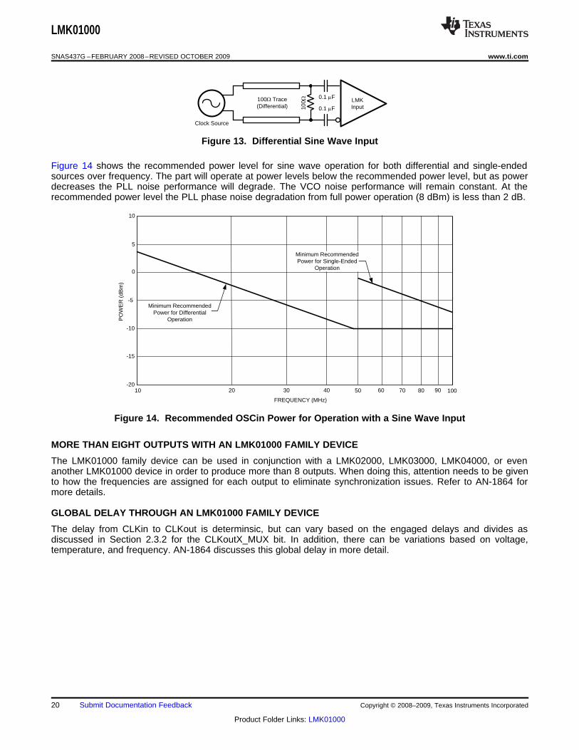
Figure 13. Differential Sine Wave Input
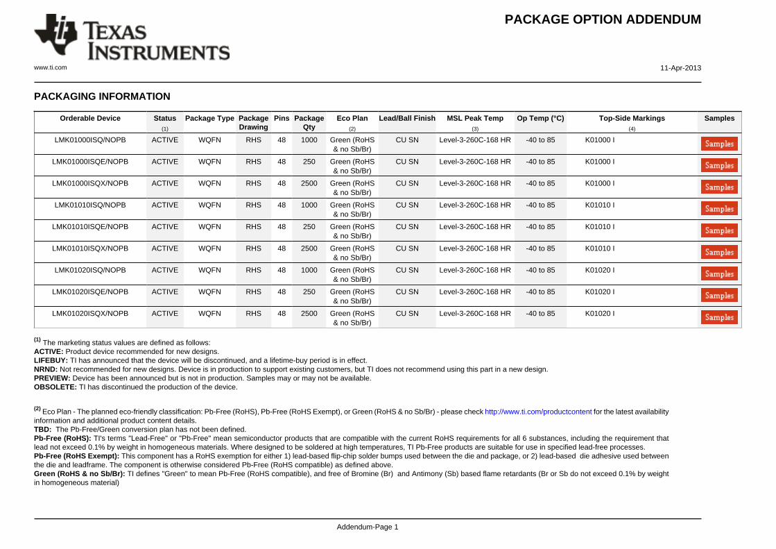
Figure 14 shows the recommended power level for sine wave operation for both differential and single-endedsources over frequency. The part will operate at power levels below the recommended power level, but as powerdecreases the PLL noise performance will degrade. The VCO noise performance will remain constant. At therecommended power level the PLL phase noise degradation from full power operation (8 dBm) is less than 2 dB.
Figure 14. Recommended OSCin Power for Operation with a Sine Wave Input
MORE THAN EIGHT OUTPUTS WITH AN LMK01000 FAMILY DEVICE
The LMK01000 family device can be used in conjunction with a LMK02000, LMK03000, LMK04000, or evenanother LMK01000 device in order to produce more than 8 outputs. When doing this, attention needs to be givento how the frequencies are assigned for each output to eliminate synchronization issues. Refer to AN-1864 formore details.
GLOBAL DELAY THROUGH AN LMK01000 FAMILY DEVICE
The delay from CLKin to CLKout is determinsic, but can vary based on the engaged delays and divides asdiscussed in Section 2.3.2 for the CLKoutX_MUX bit. In addition, there can be variations based on voltage,temperature, and frequency. AN-1864 discusses this global delay in more detail.
20 Submit Documentation Feedback Copyright © 2008–2009, Texas Instruments Incorporated
Product Folder Links: LMK01000
PACKAGE OPTION ADDENDUM
www.ti.com 11-Apr-2013
Addendum-Page 1
PACKAGING INFORMATION
Orderable Device Status(1)
Package Type PackageDrawing
Pins PackageQty
Eco Plan(2)
Lead/Ball Finish MSL Peak Temp(3)
Op Temp (°C) Top-Side Markings(4)
Samples
LMK01000ISQ/NOPB ACTIVE WQFN RHS 48 1000 Green (RoHS& no Sb/Br)
CU SN Level-3-260C-168 HR -40 to 85 K01000 I
LMK01000ISQE/NOPB ACTIVE WQFN RHS 48 250 Green (RoHS& no Sb/Br)
CU SN Level-3-260C-168 HR -40 to 85 K01000 I
LMK01000ISQX/NOPB ACTIVE WQFN RHS 48 2500 Green (RoHS& no Sb/Br)
CU SN Level-3-260C-168 HR -40 to 85 K01000 I
LMK01010ISQ/NOPB ACTIVE WQFN RHS 48 1000 Green (RoHS& no Sb/Br)
CU SN Level-3-260C-168 HR -40 to 85 K01010 I
LMK01010ISQE/NOPB ACTIVE WQFN RHS 48 250 Green (RoHS& no Sb/Br)
CU SN Level-3-260C-168 HR -40 to 85 K01010 I
LMK01010ISQX/NOPB ACTIVE WQFN RHS 48 2500 Green (RoHS& no Sb/Br)
CU SN Level-3-260C-168 HR -40 to 85 K01010 I
LMK01020ISQ/NOPB ACTIVE WQFN RHS 48 1000 Green (RoHS& no Sb/Br)
CU SN Level-3-260C-168 HR -40 to 85 K01020 I
LMK01020ISQE/NOPB ACTIVE WQFN RHS 48 250 Green (RoHS& no Sb/Br)
CU SN Level-3-260C-168 HR -40 to 85 K01020 I
LMK01020ISQX/NOPB ACTIVE WQFN RHS 48 2500 Green (RoHS& no Sb/Br)
CU SN Level-3-260C-168 HR -40 to 85 K01020 I
(1) The marketing status values are defined as follows:ACTIVE: Product device recommended for new designs.LIFEBUY: TI has announced that the device will be discontinued, and a lifetime-buy period is in effect.NRND: Not recommended for new designs. Device is in production to support existing customers, but TI does not recommend using this part in a new design.PREVIEW: Device has been announced but is not in production. Samples may or may not be available.OBSOLETE: TI has discontinued the production of the device.
(2) Eco Plan - The planned eco-friendly classification: Pb-Free (RoHS), Pb-Free (RoHS Exempt), or Green (RoHS & no Sb/Br) - please check http://www.ti.com/productcontent for the latest availabilityinformation and additional product content details.TBD: The Pb-Free/Green conversion plan has not been defined.Pb-Free (RoHS): TI's terms "Lead-Free" or "Pb-Free" mean semiconductor products that are compatible with the current RoHS requirements for all 6 substances, including the requirement thatlead not exceed 0.1% by weight in homogeneous materials. Where designed to be soldered at high temperatures, TI Pb-Free products are suitable for use in specified lead-free processes.Pb-Free (RoHS Exempt): This component has a RoHS exemption for either 1) lead-based flip-chip solder bumps used between the die and package, or 2) lead-based die adhesive used betweenthe die and leadframe. The component is otherwise considered Pb-Free (RoHS compatible) as defined above.Green (RoHS & no Sb/Br): TI defines "Green" to mean Pb-Free (RoHS compatible), and free of Bromine (Br) and Antimony (Sb) based flame retardants (Br or Sb do not exceed 0.1% by weightin homogeneous material)
PACKAGE OPTION ADDENDUM
www.ti.com 11-Apr-2013
Addendum-Page 2
(3) MSL, Peak Temp. -- The Moisture Sensitivity Level rating according to the JEDEC industry standard classifications, and peak solder temperature.
(4) Multiple Top-Side Markings will be inside parentheses. Only one Top-Side Marking contained in parentheses and separated by a "~" will appear on a device. If a line is indented then it is acontinuation of the previous line and the two combined represent the entire Top-Side Marking for that device.
Important Information and Disclaimer:The information provided on this page represents TI's knowledge and belief as of the date that it is provided. TI bases its knowledge and belief on informationprovided by third parties, and makes no representation or warranty as to the accuracy of such information. Efforts are underway to better integrate information from third parties. TI has taken andcontinues to take reasonable steps to provide representative and accurate information but may not have conducted destructive testing or chemical analysis on incoming materials and chemicals.TI and TI suppliers consider certain information to be proprietary, and thus CAS numbers and other limited information may not be available for release.
In no event shall TI's liability arising out of such information exceed the total purchase price of the TI part(s) at issue in this document sold by TI to Customer on an annual basis.
TAPE AND REEL INFORMATION
*All dimensions are nominal
Device PackageType
PackageDrawing
Pins SPQ ReelDiameter
(mm)
ReelWidth
W1 (mm)
A0(mm)
B0(mm)
K0(mm)
P1(mm)
W(mm)
Pin1Quadrant
LMK01000ISQ/NOPB WQFN RHS 48 1000 330.0 16.4 7.3 7.3 1.3 12.0 16.0 Q1
LMK01000ISQE/NOPB WQFN RHS 48 250 178.0 16.4 7.3 7.3 1.3 12.0 16.0 Q1
LMK01000ISQX/NOPB WQFN RHS 48 2500 330.0 16.4 7.3 7.3 1.3 12.0 16.0 Q1
LMK01010ISQ/NOPB WQFN RHS 48 1000 330.0 16.4 7.3 7.3 1.3 12.0 16.0 Q1
LMK01010ISQE/NOPB WQFN RHS 48 250 178.0 16.4 7.3 7.3 1.3 12.0 16.0 Q1
LMK01010ISQX/NOPB WQFN RHS 48 2500 330.0 16.4 7.3 7.3 1.3 12.0 16.0 Q1
LMK01020ISQ/NOPB WQFN RHS 48 1000 330.0 16.4 7.3 7.3 1.3 12.0 16.0 Q1
LMK01020ISQE/NOPB WQFN RHS 48 250 178.0 16.4 7.3 7.3 1.3 12.0 16.0 Q1
LMK01020ISQX/NOPB WQFN RHS 48 2500 330.0 16.4 7.3 7.3 1.3 12.0 16.0 Q1
PACKAGE MATERIALS INFORMATION
www.ti.com 12-Jun-2018
Pack Materials-Page 1
*All dimensions are nominal
Device Package Type Package Drawing Pins SPQ Length (mm) Width (mm) Height (mm)
LMK01000ISQ/NOPB WQFN RHS 48 1000 367.0 367.0 38.0
LMK01000ISQE/NOPB WQFN RHS 48 250 210.0 185.0 35.0
LMK01000ISQX/NOPB WQFN RHS 48 2500 367.0 367.0 38.0
LMK01010ISQ/NOPB WQFN RHS 48 1000 367.0 367.0 38.0
LMK01010ISQE/NOPB WQFN RHS 48 250 210.0 185.0 35.0
LMK01010ISQX/NOPB WQFN RHS 48 2500 367.0 367.0 38.0
LMK01020ISQ/NOPB WQFN RHS 48 1000 367.0 367.0 38.0
LMK01020ISQE/NOPB WQFN RHS 48 250 210.0 185.0 35.0
LMK01020ISQX/NOPB WQFN RHS 48 2500 367.0 367.0 38.0
PACKAGE MATERIALS INFORMATION
www.ti.com 12-Jun-2018
Pack Materials-Page 2
www.ti.com
PACKAGE OUTLINE
C
SEE TERMINALDETAIL
48X 0.300.18
5.1 0.1
48X 0.50.3
0.80.7
(A) TYP
0.050.00
44X 0.5
2X5.5
2X 5.5
A 7.156.85
B
7.156.85
0.300.18
0.50.3
(0.2)
WQFN - 0.8 mm max heightRHS0048APLASTIC QUAD FLATPACK - NO LEAD
4214990/B 04/2018
DIM AOPT 1 OPT 2(0.1) (0.2)
PIN 1 INDEX AREA
0.08 C
SEATING PLANE
1
1225
36
13 24
48 37
(OPTIONAL)PIN 1 ID 0.1 C A B
0.05
EXPOSEDTHERMAL PAD
49 SYMM
SYMM
NOTES: 1. All linear dimensions are in millimeters. Any dimensions in parenthesis are for reference only. Dimensioning and tolerancing per ASME Y14.5M. 2. This drawing is subject to change without notice. 3. The package thermal pad must be soldered to the printed circuit board for thermal and mechanical performance.
SCALE 1.800
DETAILOPTIONAL TERMINAL
TYPICAL
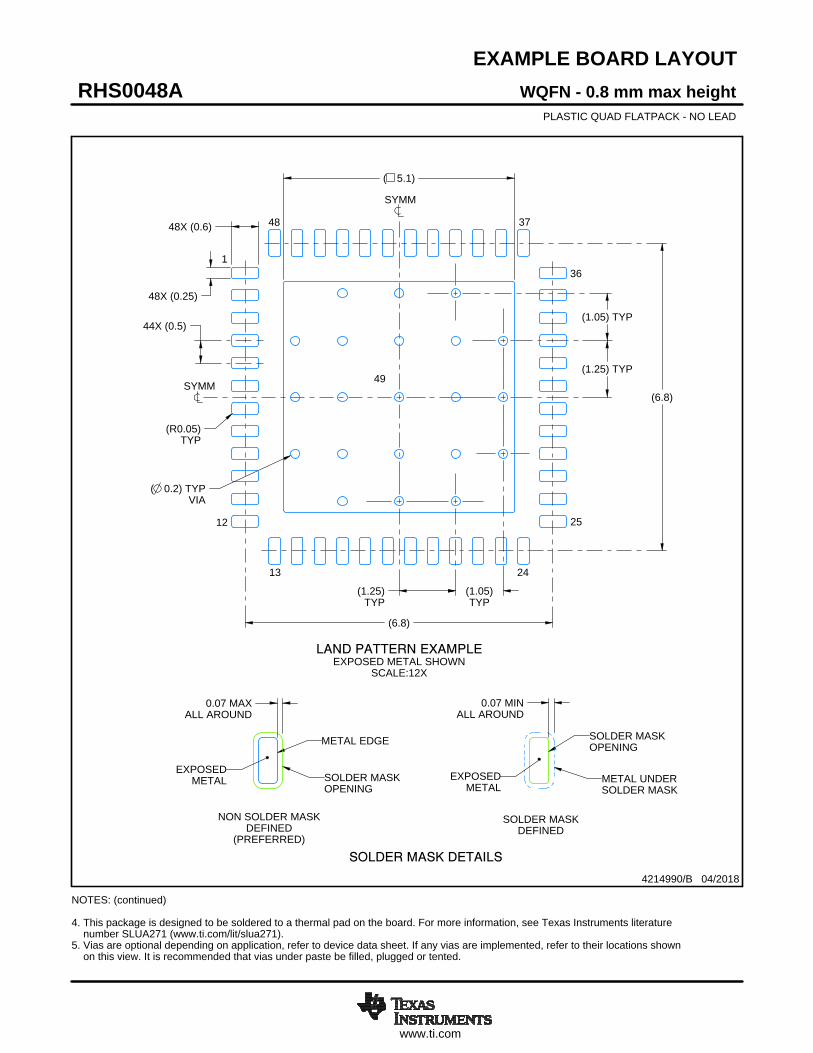
www.ti.com
EXAMPLE BOARD LAYOUT
0.07 MINALL AROUND
0.07 MAXALL AROUND
48X (0.25)
48X (0.6)
( 0.2) TYPVIA
44X (0.5)
(6.8)
(6.8)
(1.25) TYP
( 5.1)
(R0.05)TYP
(1.25)TYP
(1.05) TYP
(1.05)TYP
WQFN - 0.8 mm max heightRHS0048APLASTIC QUAD FLATPACK - NO LEAD
4214990/B 04/2018
SYMM
1
12
13 24
25
36
3748
SYMM
LAND PATTERN EXAMPLEEXPOSED METAL SHOWN
SCALE:12X
NOTES: (continued) 4. This package is designed to be soldered to a thermal pad on the board. For more information, see Texas Instruments literature number SLUA271 (www.ti.com/lit/slua271).5. Vias are optional depending on application, refer to device data sheet. If any vias are implemented, refer to their locations shown on this view. It is recommended that vias under paste be filled, plugged or tented.
49
SOLDER MASKOPENING
METAL UNDERSOLDER MASK
SOLDER MASKDEFINED
EXPOSEDMETAL
METAL EDGE
SOLDER MASKOPENING
SOLDER MASK DETAILS
NON SOLDER MASKDEFINED
(PREFERRED)
EXPOSEDMETAL
www.ti.com
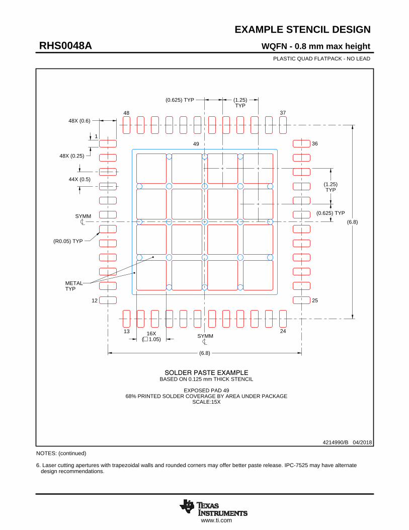
EXAMPLE STENCIL DESIGN
48X (0.6)
48X (0.25)
44X (0.5)
(6.8)
(6.8)
16X( 1.05)
(0.625) TYP
(R0.05) TYP
(1.25)TYP
(1.25)TYP
(0.625) TYP
WQFN - 0.8 mm max heightRHS0048APLASTIC QUAD FLATPACK - NO LEAD
4214990/B 04/2018
NOTES: (continued) 6. Laser cutting apertures with trapezoidal walls and rounded corners may offer better paste release. IPC-7525 may have alternate design recommendations.
49
SYMM
METALTYP
SOLDER PASTE EXAMPLEBASED ON 0.125 mm THICK STENCIL
EXPOSED PAD 49
68% PRINTED SOLDER COVERAGE BY AREA UNDER PACKAGESCALE:15X
SYMM
1
12
13 24
25
36
3748
IMPORTANT NOTICE
Texas Instruments Incorporated (TI) reserves the right to make corrections, enhancements, improvements and other changes to itssemiconductor products and services per JESD46, latest issue, and to discontinue any product or service per JESD48, latest issue. Buyersshould obtain the latest relevant information before placing orders and should verify that such information is current and complete.TI’s published terms of sale for semiconductor products (http://www.ti.com/sc/docs/stdterms.htm) apply to the sale of packaged integratedcircuit products that TI has qualified and released to market. Additional terms may apply to the use or sale of other types of TI products andservices.Reproduction of significant portions of TI information in TI data sheets is permissible only if reproduction is without alteration and isaccompanied by all associated warranties, conditions, limitations, and notices. TI is not responsible or liable for such reproduceddocumentation. Information of third parties may be subject to additional restrictions. Resale of TI products or services with statementsdifferent from or beyond the parameters stated by TI for that product or service voids all express and any implied warranties for theassociated TI product or service and is an unfair and deceptive business practice. TI is not responsible or liable for any such statements.Buyers and others who are developing systems that incorporate TI products (collectively, “Designers”) understand and agree that Designersremain responsible for using their independent analysis, evaluation and judgment in designing their applications and that Designers havefull and exclusive responsibility to assure the safety of Designers' applications and compliance of their applications (and of all TI productsused in or for Designers’ applications) with all applicable regulations, laws and other applicable requirements. Designer represents that, withrespect to their applications, Designer has all the necessary expertise to create and implement safeguards that (1) anticipate dangerousconsequences of failures, (2) monitor failures and their consequences, and (3) lessen the likelihood of failures that might cause harm andtake appropriate actions. Designer agrees that prior to using or distributing any applications that include TI products, Designer willthoroughly test such applications and the functionality of such TI products as used in such applications.TI’s provision of technical, application or other design advice, quality characterization, reliability data or other services or information,including, but not limited to, reference designs and materials relating to evaluation modules, (collectively, “TI Resources”) are intended toassist designers who are developing applications that incorporate TI products; by downloading, accessing or using TI Resources in anyway, Designer (individually or, if Designer is acting on behalf of a company, Designer’s company) agrees to use any particular TI Resourcesolely for this purpose and subject to the terms of this Notice.TI’s provision of TI Resources does not expand or otherwise alter TI’s applicable published warranties or warranty disclaimers for TIproducts, and no additional obligations or liabilities arise from TI providing such TI Resources. TI reserves the right to make corrections,enhancements, improvements and other changes to its TI Resources. TI has not conducted any testing other than that specificallydescribed in the published documentation for a particular TI Resource.Designer is authorized to use, copy and modify any individual TI Resource only in connection with the development of applications thatinclude the TI product(s) identified in such TI Resource. NO OTHER LICENSE, EXPRESS OR IMPLIED, BY ESTOPPEL OR OTHERWISETO ANY OTHER TI INTELLECTUAL PROPERTY RIGHT, AND NO LICENSE TO ANY TECHNOLOGY OR INTELLECTUAL PROPERTYRIGHT OF TI OR ANY THIRD PARTY IS GRANTED HEREIN, including but not limited to any patent right, copyright, mask work right, orother intellectual property right relating to any combination, machine, or process in which TI products or services are used. Informationregarding or referencing third-party products or services does not constitute a license to use such products or services, or a warranty orendorsement thereof. Use of TI Resources may require a license from a third party under the patents or other intellectual property of thethird party, or a license from TI under the patents or other intellectual property of TI.TI RESOURCES ARE PROVIDED “AS IS” AND WITH ALL FAULTS. TI DISCLAIMS ALL OTHER WARRANTIES ORREPRESENTATIONS, EXPRESS OR IMPLIED, REGARDING RESOURCES OR USE THEREOF, INCLUDING BUT NOT LIMITED TOACCURACY OR COMPLETENESS, TITLE, ANY EPIDEMIC FAILURE WARRANTY AND ANY IMPLIED WARRANTIES OFMERCHANTABILITY, FITNESS FOR A PARTICULAR PURPOSE, AND NON-INFRINGEMENT OF ANY THIRD PARTY INTELLECTUALPROPERTY RIGHTS. TI SHALL NOT BE LIABLE FOR AND SHALL NOT DEFEND OR INDEMNIFY DESIGNER AGAINST ANY CLAIM,INCLUDING BUT NOT LIMITED TO ANY INFRINGEMENT CLAIM THAT RELATES TO OR IS BASED ON ANY COMBINATION OFPRODUCTS EVEN IF DESCRIBED IN TI RESOURCES OR OTHERWISE. IN NO EVENT SHALL TI BE LIABLE FOR ANY ACTUAL,DIRECT, SPECIAL, COLLATERAL, INDIRECT, PUNITIVE, INCIDENTAL, CONSEQUENTIAL OR EXEMPLARY DAMAGES INCONNECTION WITH OR ARISING OUT OF TI RESOURCES OR USE THEREOF, AND REGARDLESS OF WHETHER TI HAS BEENADVISED OF THE POSSIBILITY OF SUCH DAMAGES.Unless TI has explicitly designated an individual product as meeting the requirements of a particular industry standard (e.g., ISO/TS 16949and ISO 26262), TI is not responsible for any failure to meet such industry standard requirements.Where TI specifically promotes products as facilitating functional safety or as compliant with industry functional safety standards, suchproducts are intended to help enable customers to design and create their own applications that meet applicable functional safety standardsand requirements. Using products in an application does not by itself establish any safety features in the application. Designers mustensure compliance with safety-related requirements and standards applicable to their applications. Designer may not use any TI products inlife-critical medical equipment unless authorized officers of the parties have executed a special contract specifically governing such use.Life-critical medical equipment is medical equipment where failure of such equipment would cause serious bodily injury or death (e.g., lifesupport, pacemakers, defibrillators, heart pumps, neurostimulators, and implantables). Such equipment includes, without limitation, allmedical devices identified by the U.S. Food and Drug Administration as Class III devices and equivalent classifications outside the U.S.TI may expressly designate certain products as completing a particular qualification (e.g., Q100, Military Grade, or Enhanced Product).Designers agree that it has the necessary expertise to select the product with the appropriate qualification designation for their applicationsand that proper product selection is at Designers’ own risk. Designers are solely responsible for compliance with all legal and regulatoryrequirements in connection with such selection.Designer will fully indemnify TI and its representatives against any damages, costs, losses, and/or liabilities arising out of Designer’s non-compliance with the terms and provisions of this Notice.
Mailing Address: Texas Instruments, Post Office Box 655303, Dallas, Texas 75265Copyright © 2018, Texas Instruments Incorporated