Embed Size (px)
Citation preview
Materials Chemistry and Physics 75 (2002) 235–240
Low temperature oxidation of CVD SiC by electroncyclotron resonance plasma
Takashi Goto∗, Hiroshi Masumoto, Mineo NiizumaInstitute for Materials Research, Tohoku University, Sendai 980-8577, Japan
Abstract
The oxidation behavior in electron cyclotron resonance (ECR) plasma-enhanced oxygen plasma for Si- and C-faces of CVD SiC wasstudied at 398–873 K. In pure O2 gas, the oxidation kinetics are parabolic and logarithmic for the C- and Si-faces, respectively. Monolithicamorphous SiO2 layers were formed on the Si-face, but mixtures of outer SiO2 and inner Si–C–O layers were observed on the C-face.In an Ar–O2 gas mixture, there was no difference in oxidation behavior between Si- and C-faces. The oxidation kinetics were linear, andnano-meter size crystalline Si particles were found dispersed in the amorphous SiO2 layers. © 2002 Elsevier Science B.V. All rights reserved.
Keywords: CVD SiC; Oxidation; Electron cyclotron resonance plasma; Nano silicon
1. Introduction
Silicon carbide (SiC) has been intensively studied becauseof its potential as a high-temperature structural material,due to excellent high-temperature strength, thermal shockresistance and oxidation resistance. The fabrication process,such as pressure-less sintering, hot-pressing (HP) and chem-ical vapor deposition (CVD), often significantly affects thecharacteristics of SiC, because impurity content and micro-structure strongly depend on the fabrication process. Inparticular, it is known that the oxidation resistance improveswith decreasing impurity content [1]. The CVD process isadvantageous in the preparation of high purity material, andtherefore CVD SiC is expected to exhibit superior oxidationprotective coatings for applications such as a nose cone for aspace vehicle and an inner wall of a combustion chamber [2].
The crystal structure of SiC is basically constructed fromthe stacking of Si- and C-atom layers. Using single crystal�-SiC, the oxidation rates of C-atom layer (C-face) werefound to be higher than those of Si-atom layer (Si-face), andthe difference of oxidation rates became more significantwith decreasing temperature [3].
It is accepted that CVD SiC has a cubic structure, and the(1 1 1) plane of CVD SiC is often preferentially oriented par-allel to the substrate [4]. The surface of the strongly (1 1 1)oriented CVD SiC would be either Si- or C-face. There-fore, it is important to understand the oxidation behavior ofSi- and C-faces for any applications of the CVD SiC.
∗ Corresponding author.E-mail address: [email protected] (T. Goto).
CVD SiC also has a great potential as a new high-powermetal-oxide–semiconductor-field transistor (MOSFET)device [5]. For this application, a low temperature oxida-tion process is essential to prevent the diffusion of dopingelements in SiC, and highly insulative gate oxide layersneed to be formed on the SiC surface at as low a temper-ature as possible. So far several attempts have been madeto oxidize high purity single crystalline or CVD SiC at lowtemperatures using ion irradiation [6], ozone oxidation [7]and radio frequency (RF) plasma oxidation [8]. However,the oxidation rates of these methods are insufficient at lowtemperatures, less than 1000 K.
Since electron cyclotron resonance (ECR) plasma is ableto produce highly activated oxygen ions, CVD SiC may bereadily oxidized by ECR enhanced plasma at low tempera-tures. In this paper, (1 1 1) oriented CVD SiC was oxidizedin the ECR plasma, and the oxidation behavior of Si- andC-faces of CVD SiC studied.
2. Experimental procedure
Yellow colored translucent CVD SiC plates (�-type:Admap) with the impurity levels of ppb (according to themanufacturer’s analysis) were used as specimens. X-raydiffraction (XRD) analyses showed that the specimens werealmost perfectly (1 1 1) oriented; the surface of the speci-mens was then assumed to be either the Si- or C-face. Theactual faces of the surface were determined by pre-oxidationexperiments, because the C-face was known to be moreeasily oxidized than Si-face. The specimens were cut to
0254-0584/02/$ – see front matter © 2002 Elsevier Science B.V. All rights reserved.PII: S0254-0584(02)00068-8
236 T. Goto et al. / Materials Chemistry and Physics 75 (2002) 235–240
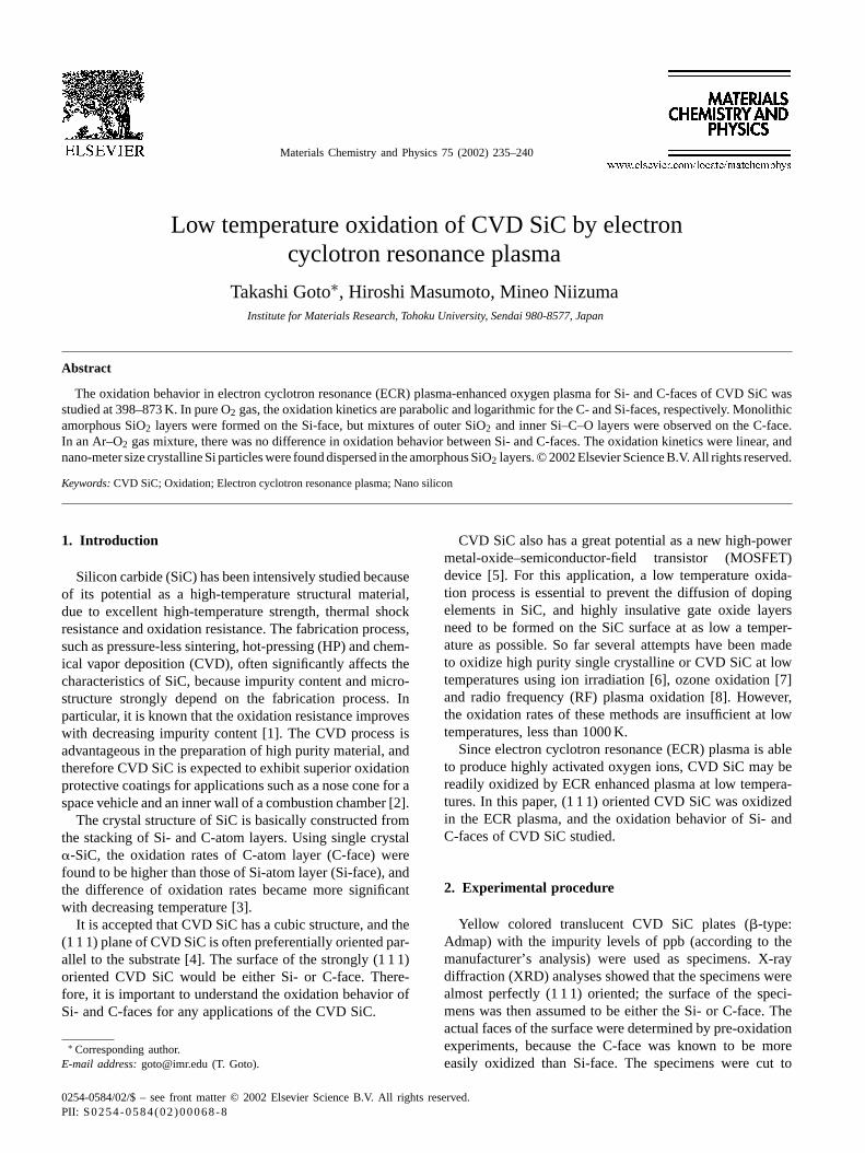
Fig. 1. A schematic diagram of the ECR plasma chamber.
10 mm× 10 mm× 0.6 mm, mirror polished, immersed inHF–HNO3 solution, and rinsed in acetone. Fig. 1 depicts aschematic diagram of the ECR plasma chamber (Sumitomometals: ES037) that was evacuated up to 1× 10⁻⁴ Pa witha turbo molecular pump. The total pressure in the chamberwas maintained at 5× 10⁻² Pa by introducing pure O2 oran Ar–O2 mixture gas (Ar/O2 = 100/1). A microwave(frequency: 2.45 GHz, power: 900 W) was conducted intothe chamber through a waveguide, and a magnetic field(intensity: 8.75 × 10⁻² T) was applied to satisfy an ECRcondition. The specimens were heated by an infrared lampat temperatures of 398–873 K for 600–14.4 ks. The thick-ness and refractive index of the oxide layers formed by theECR oxidation were measured by ellipsometry (Gaetner:L116-13). The structure and composition of the oxidelayers were examined by XRD (Rigaku: RAD-C), Augerelectron spectroscopy (AES) (JEOL: JAMP-7100E), X-rayphoto-electron spectroscopy (XPS) (SSI: SSX-100), sec-ondary ion mass spectroscopy (SIMS) (ALVAC-PHAI:6600) and transmission electron microscopy (TEM) (JEOL:JEM-2000FX).
3. Results and discussion
3.1. ECR plasma oxidation in pure O2 atmosphere
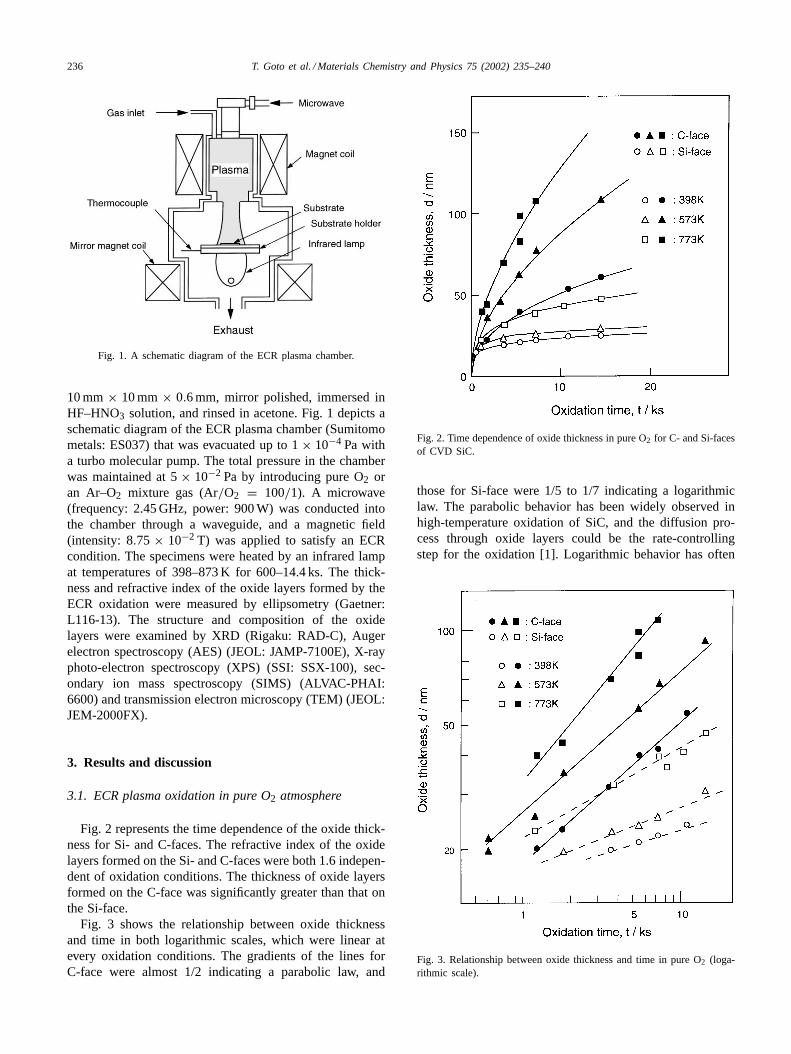
Fig. 2 represents the time dependence of the oxide thick-ness for Si- and C-faces. The refractive index of the oxidelayers formed on the Si- and C-faces were both 1.6 indepen-dent of oxidation conditions. The thickness of oxide layersformed on the C-face was significantly greater than that onthe Si-face.
Fig. 3 shows the relationship between oxide thicknessand time in both logarithmic scales, which were linear atevery oxidation conditions. The gradients of the lines forC-face were almost 1/2 indicating a parabolic law, and
Fig. 2. Time dependence of oxide thickness in pure O2 for C- and Si-facesof CVD SiC.
those for Si-face were 1/5 to 1/7 indicating a logarithmiclaw. The parabolic behavior has been widely observed inhigh-temperature oxidation of SiC, and the diffusion pro-cess through oxide layers could be the rate-controllingstep for the oxidation [1]. Logarithmic behavior has often
Fig. 3. Relationship between oxide thickness and time in pure O2 (loga-rithmic scale).
T. Goto et al. / Materials Chemistry and Physics 75 (2002) 235–240 237
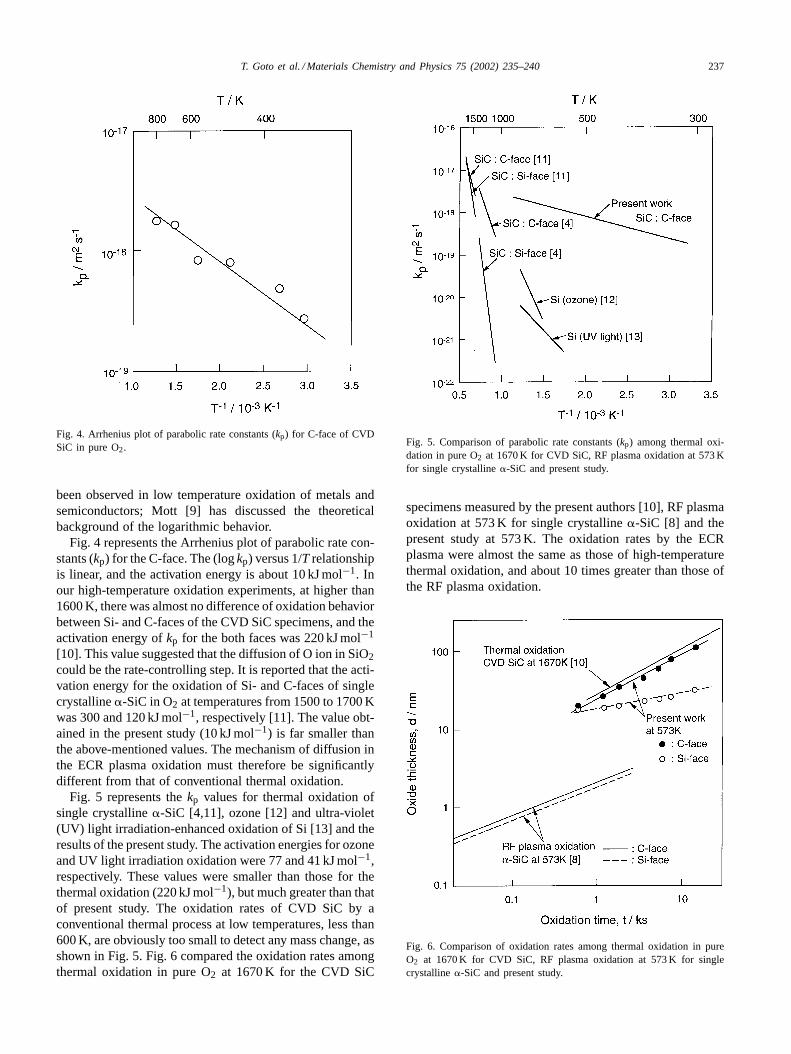
Fig. 4. Arrhenius plot of parabolic rate constants (kp) for C-face of CVDSiC in pure O2.
been observed in low temperature oxidation of metals andsemiconductors; Mott [9] has discussed the theoreticalbackground of the logarithmic behavior.
Fig. 4 represents the Arrhenius plot of parabolic rate con-stants (kp) for the C-face. The (logkp) versus 1/T relationshipis linear, and the activation energy is about 10 kJ mol−1. Inour high-temperature oxidation experiments, at higher than1600 K, there was almost no difference of oxidation behaviorbetween Si- and C-faces of the CVD SiC specimens, and theactivation energy ofkp for the both faces was 220 kJ mol−1
[10]. This value suggested that the diffusion of O ion in SiO2could be the rate-controlling step. It is reported that the acti-vation energy for the oxidation of Si- and C-faces of singlecrystalline�-SiC in O2 at temperatures from 1500 to 1700 Kwas 300 and 120 kJ mol−1, respectively [11]. The value obt-ained in the present study (10 kJ mol−1) is far smaller thanthe above-mentioned values. The mechanism of diffusion inthe ECR plasma oxidation must therefore be significantlydifferent from that of conventional thermal oxidation.
Fig. 5 represents thekp values for thermal oxidation ofsingle crystalline�-SiC [4,11], ozone [12] and ultra-violet(UV) light irradiation-enhanced oxidation of Si [13] and theresults of the present study. The activation energies for ozoneand UV light irradiation oxidation were 77 and 41 kJ mol−1,respectively. These values were smaller than those for thethermal oxidation (220 kJ mol−1), but much greater than thatof present study. The oxidation rates of CVD SiC by aconventional thermal process at low temperatures, less than600 K, are obviously too small to detect any mass change, asshown in Fig. 5. Fig. 6 compared the oxidation rates amongthermal oxidation in pure O2 at 1670 K for the CVD SiC
Fig. 5. Comparison of parabolic rate constants (kp) among thermal oxi-dation in pure O2 at 1670 K for CVD SiC, RF plasma oxidation at 573 Kfor single crystalline�-SiC and present study.
specimens measured by the present authors [10], RF plasmaoxidation at 573 K for single crystalline�-SiC [8] and thepresent study at 573 K. The oxidation rates by the ECRplasma were almost the same as those of high-temperaturethermal oxidation, and about 10 times greater than those ofthe RF plasma oxidation.
Fig. 6. Comparison of oxidation rates among thermal oxidation in pureO2 at 1670 K for CVD SiC, RF plasma oxidation at 573 K for singlecrystalline�-SiC and present study.
238 T. Goto et al. / Materials Chemistry and Physics 75 (2002) 235–240
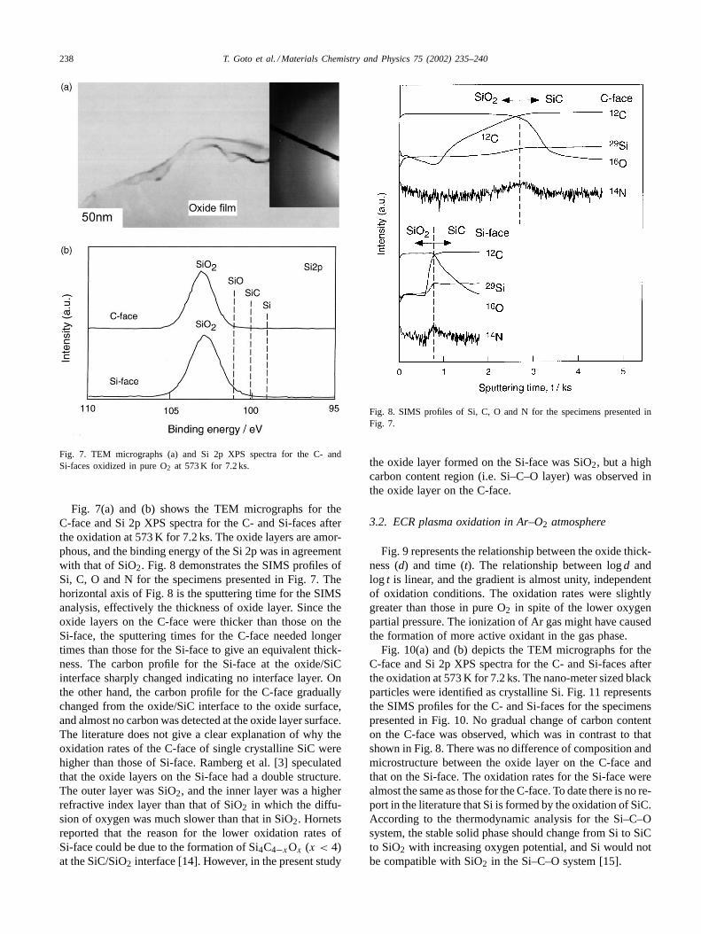
Fig. 7. TEM micrographs (a) and Si 2p XPS spectra for the C- andSi-faces oxidized in pure O2 at 573 K for 7.2 ks.
Fig. 7(a) and (b) shows the TEM micrographs for theC-face and Si 2p XPS spectra for the C- and Si-faces afterthe oxidation at 573 K for 7.2 ks. The oxide layers are amor-phous, and the binding energy of the Si 2p was in agreementwith that of SiO2. Fig. 8 demonstrates the SIMS profiles ofSi, C, O and N for the specimens presented in Fig. 7. Thehorizontal axis of Fig. 8 is the sputtering time for the SIMSanalysis, effectively the thickness of oxide layer. Since theoxide layers on the C-face were thicker than those on theSi-face, the sputtering times for the C-face needed longertimes than those for the Si-face to give an equivalent thick-ness. The carbon profile for the Si-face at the oxide/SiCinterface sharply changed indicating no interface layer. Onthe other hand, the carbon profile for the C-face graduallychanged from the oxide/SiC interface to the oxide surface,and almost no carbon was detected at the oxide layer surface.The literature does not give a clear explanation of why theoxidation rates of the C-face of single crystalline SiC werehigher than those of Si-face. Ramberg et al. [3] speculatedthat the oxide layers on the Si-face had a double structure.The outer layer was SiO2, and the inner layer was a higherrefractive index layer than that of SiO2 in which the diffu-sion of oxygen was much slower than that in SiO2. Hornetsreported that the reason for the lower oxidation rates ofSi-face could be due to the formation of Si4C4−xOx (x < 4)at the SiC/SiO2 interface [14]. However, in the present study
Fig. 8. SIMS profiles of Si, C, O and N for the specimens presented inFig. 7.
the oxide layer formed on the Si-face was SiO2, but a highcarbon content region (i.e. Si–C–O layer) was observed inthe oxide layer on the C-face.
3.2. ECR plasma oxidation in Ar–O2 atmosphere
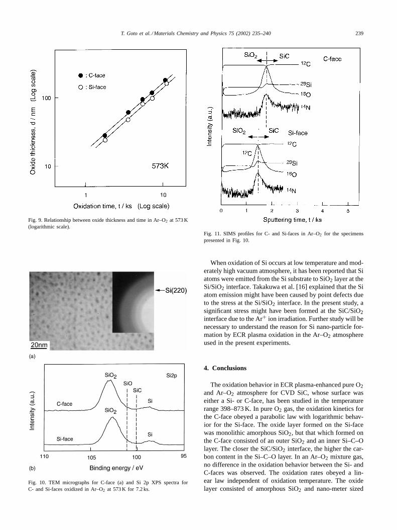
Fig. 9 represents the relationship between the oxide thick-ness (d) and time (t). The relationship between logd andlog t is linear, and the gradient is almost unity, independentof oxidation conditions. The oxidation rates were slightlygreater than those in pure O2 in spite of the lower oxygenpartial pressure. The ionization of Ar gas might have causedthe formation of more active oxidant in the gas phase.
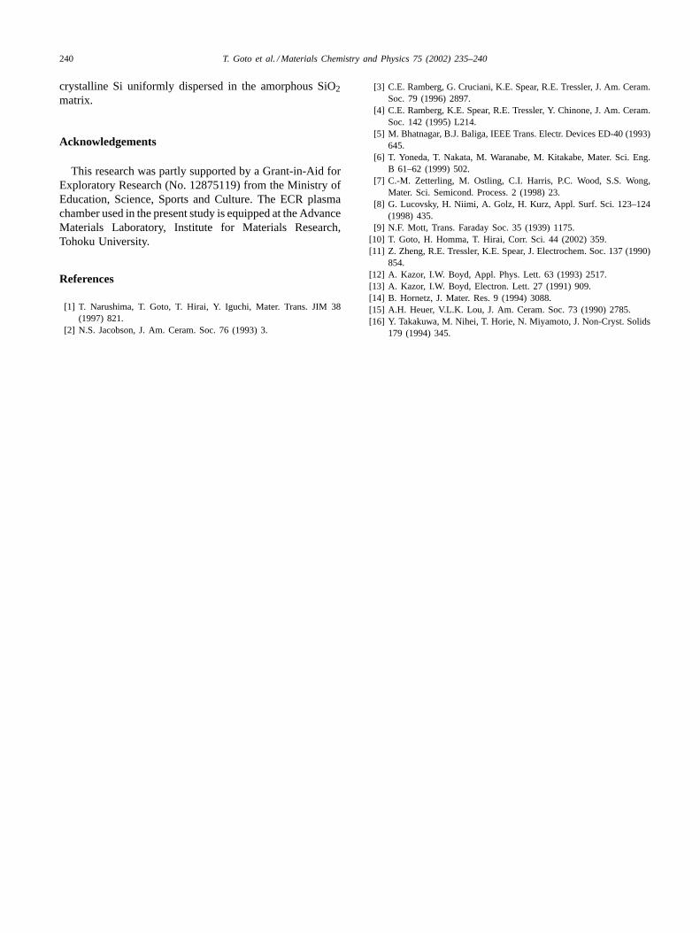
Fig. 10(a) and (b) depicts the TEM micrographs for theC-face and Si 2p XPS spectra for the C- and Si-faces afterthe oxidation at 573 K for 7.2 ks. The nano-meter sized blackparticles were identified as crystalline Si. Fig. 11 representsthe SIMS profiles for the C- and Si-faces for the specimenspresented in Fig. 10. No gradual change of carbon contenton the C-face was observed, which was in contrast to thatshown in Fig. 8. There was no difference of composition andmicrostructure between the oxide layer on the C-face andthat on the Si-face. The oxidation rates for the Si-face werealmost the same as those for the C-face. To date there is no re-port in the literature that Si is formed by the oxidation of SiC.According to the thermodynamic analysis for the Si–C–Osystem, the stable solid phase should change from Si to SiCto SiO2 with increasing oxygen potential, and Si would notbe compatible with SiO2 in the Si–C–O system [15].
T. Goto et al. / Materials Chemistry and Physics 75 (2002) 235–240 239
Fig. 9. Relationship between oxide thickness and time in Ar–O2 at 573 K(logarithmic scale).
Fig. 10. TEM micrographs for C-face (a) and Si 2p XPS spectra forC- and Si-faces oxidized in Ar–O2 at 573 K for 7.2 ks.
Fig. 11. SIMS profiles for C- and Si-faces in Ar–O2 for the specimenspresented in Fig. 10.
When oxidation of Si occurs at low temperature and mod-erately high vacuum atmosphere, it has been reported that Siatoms were emitted from the Si substrate to SiO2 layer at theSi/SiO2 interface. Takakuwa et al. [16] explained that the Siatom emission might have been caused by point defects dueto the stress at the Si/SiO2 interface. In the present study, asignificant stress might have been formed at the SiC/SiO2interface due to the Ar+ ion irradiation. Further study will benecessary to understand the reason for Si nano-particle for-mation by ECR plasma oxidation in the Ar–O2 atmosphereused in the present experiments.
4. Conclusions
The oxidation behavior in ECR plasma-enhanced pure O2and Ar–O2 atmosphere for CVD SiC, whose surface waseither a Si- or C-face, has been studied in the temperaturerange 398–873 K. In pure O2 gas, the oxidation kinetics forthe C-face obeyed a parabolic law with logarithmic behav-ior for the Si-face. The oxide layer formed on the Si-facewas monolithic amorphous SiO2, but that which formed onthe C-face consisted of an outer SiO2 and an inner Si–C–Olayer. The closer the SiC/SiO2 interface, the higher the car-bon content in the Si–C–O layer. In an Ar–O2 mixture gas,no difference in the oxidation behavior between the Si- andC-faces was observed. The oxidation rates obeyed a lin-ear law independent of oxidation temperature. The oxidelayer consisted of amorphous SiO2 and nano-meter sized
240 T. Goto et al. / Materials Chemistry and Physics 75 (2002) 235–240
crystalline Si uniformly dispersed in the amorphous SiO2matrix.
Acknowledgements
This research was partly supported by a Grant-in-Aid forExploratory Research (No. 12875119) from the Ministry ofEducation, Science, Sports and Culture. The ECR plasmachamber used in the present study is equipped at the AdvanceMaterials Laboratory, Institute for Materials Research,Tohoku University.
References
[1] T. Narushima, T. Goto, T. Hirai, Y. Iguchi, Mater. Trans. JIM 38(1997) 821.
[2] N.S. Jacobson, J. Am. Ceram. Soc. 76 (1993) 3.
[3] C.E. Ramberg, G. Cruciani, K.E. Spear, R.E. Tressler, J. Am. Ceram.Soc. 79 (1996) 2897.
[4] C.E. Ramberg, K.E. Spear, R.E. Tressler, Y. Chinone, J. Am. Ceram.Soc. 142 (1995) L214.
[5] M. Bhatnagar, B.J. Baliga, IEEE Trans. Electr. Devices ED-40 (1993)645.
[6] T. Yoneda, T. Nakata, M. Waranabe, M. Kitakabe, Mater. Sci. Eng.B 61–62 (1999) 502.
[7] C.-M. Zetterling, M. Ostling, C.I. Harris, P.C. Wood, S.S. Wong,Mater. Sci. Semicond. Process. 2 (1998) 23.
[8] G. Lucovsky, H. Niimi, A. Golz, H. Kurz, Appl. Surf. Sci. 123–124(1998) 435.
[9] N.F. Mott, Trans. Faraday Soc. 35 (1939) 1175.[10] T. Goto, H. Homma, T. Hirai, Corr. Sci. 44 (2002) 359.[11] Z. Zheng, R.E. Tressler, K.E. Spear, J. Electrochem. Soc. 137 (1990)
854.[12] A. Kazor, I.W. Boyd, Appl. Phys. Lett. 63 (1993) 2517.[13] A. Kazor, I.W. Boyd, Electron. Lett. 27 (1991) 909.[14] B. Hornetz, J. Mater. Res. 9 (1994) 3088.[15] A.H. Heuer, V.L.K. Lou, J. Am. Ceram. Soc. 73 (1990) 2785.[16] Y. Takakuwa, M. Nihei, T. Horie, N. Miyamoto, J. Non-Cryst. Solids
179 (1994) 345.


![JoiningofC /SiCCeramicMatrixComposites:AReview · 2018. 3. 1. · Rizzo et al. [48] reported that a CVD-SiC coated C f/SiC composite was directly joined to its coun-terparts using](https://img.pdfslide.net/doc/110x75/6125d87a77b3002268280c66/joiningofc-sicceramicmatrixcompositesareview-2018-3-1-rizzo-et-al-48-reported.jpg)