Embed Size (px)
Citation preview

1
LTC1479
PowerPath Controllerfor Dual Battery Systems
FEATURES DESCRIPTION
U
Complete Power Path Management for TwoBatteries, DC Power Source, Charger and Backup
Compatible with Li-Ion, NiCd, NiMH and Lead-AcidBattery Chemistries
“3-Diode” Mode Ensures Powers is Availableunder “Cold Start” Conditions
All N-Channel Switching Reduces Power Losses Capacitor and Battery Inrush Current Limited “Seamless” Switching Between Power Sources Independent Charging and Monitoring of Two
Battery Packs New, Small Footprint, 36-Lead SSOP Package
The LTC®1479 is the “heart” of a total power managementsolution for single and dual battery notebook computersand other portable equipment. The LTC1479 directs powerfrom up to two battery packs and a DC power source to theinput of the main system switching regulator. It works inconcert with related LTC power management products(e.g. LTC1435, LT®1511, etc.) to create a total systemsolution; starting from the batteries and the DC powersource, and ending at the input of each of the computer’scomplex loads. A system-provided power managementµP monitors and actively directs the LTC1479.
The LTC1479 uses low loss N-channel MOSFET switchesto direct power from three main sources. An adaptivecurrent limiting scheme reduces capacitor and batteryinrush current by controlling the gates of the MOSFETswitches during transitions. The LTC1479 interfaces di-rectly to the LT1510, LT1511 and LT1620/LTC1435 bat-tery charging circuits.
TYPICAL APPLICATION
U
Dual Battery PowerPathTM Controller System Block Diagram
PowerPath is a trademark of Linear Technology Corporation., LTC and LT are registered trademarks of Linear Technology Corporation.
Notebook Computer Power Management Portable Instruments Handheld Terminals Portable Medical Equipment Portable Industrial Control Equipment
APPLICATIONSU
BAT1
BAT2BATTERY CHARGER
(LT1510/LT1511/ LT1620/LTC1435)
SW A/B
RSENSESW C/D
SW E/F
SW G SW H
+CIN
DCIN
1479 TA01
5V
AC ADAPTER
POWER MANAGEMENT
µP
BACKUP REGULATOR
(LT1304)
HIGH EFFICIENCY DC/DC SWITCHING
REGULATOR (LTC1435/LTC1438
ETC.)
LTC1479 PowerPath CONTROLLER
STATUS & CONTROL

2
LTC1479
ABSOLUTE MAXIMUM RATINGS
W WW U
PACKAGE/ORDER INFORMATION
W UU
ORDER PARTNUMBER
TJMAX = 100°C, θJA = 95°C/ W
Consult factory for Military grade parts.
1
2
3
4
5
6
7
8
9
10
11
12
13
14
15
16
17
18
TOP VIEW
G PACKAGE (209 mils) 36-LEAD PLASTIC SSOP
36
35
34
33
32
31
30
29
28
27
26
25
24
23
22
21
20
19
DCIN
DCDIV
LOBAT
GA
SAB
GB
GC
SCD
GD
GE
SEF
GF
SENSE+
SENSE–
VCC
VGG
V+
SW
VBKUP
BAT1
BAT2
BDIV
VBAT
CHGMON
BATSEL
GG
SG
GH
SH
DCINGOOD
DCIN/BAT
BATDIS
3DM
CHGSEL
VCCP
GND
DCIN, BAT1, BAT2 Supply Voltages .......... –0.3V to 32VSENSE +, SENSE–, VBAT, V + ..................... –0.3V to 32VGA, GB, GC, GD, GE, GF, GG, GH .............. –0.3V to 42VSAB, SCD, SEF, SG, SH ............................ –0.3V to 32VSW, VGG ................................................... –0.3V to 42VDCDIV, BDIV ............................................ –0.3V to 5.5VAll Logic Inputs (Note 1).......................... –0.3V to 7.5VAll Logic Outputs (Note 1) ....................... –0.3V to 7.5VVCC Regulator Output Current ................................ 1mAVCCP Regulator Output Current .............................. 1mAV+ Output Current .................................................. 1mAVGG Regulator Output Current ............................ 100µAOperating Temperature
LTC1479CG ............................................. 0°C to 70°CLTC1479IG ........................................ – 40°C to 85°C
Junction Temperature........................................... 125°CStorage Temperature Range ................. –65°C to 150°CLead Temperature (Soldering, 10 sec).................. 300°C
SYMBOL PARAMETER CONDITIONS MIN TYP MAX UNITS
Power Supplies
VDCIN DCIN Operating Range (Mode 1) DCIN Selected 6 28 V
VBAT1 Battery 1 Operating Range (Mode 5) Battery 1 Selected 6 28 V
VBAT2 Battery 2 Operating Range (Mode 6) Battery 2 Selected 6 28 V
VBKUP Backup Operating Range (Mode 8) Backup Operation 6 28 V
IDCIN DCIN Operating Current (Mode 1) DCIN Selected 175 500 µA
IVBAT1 Battery 1 Operating Current (Mode 5) Battery 1 Selected 150 500 µA
IVBAT2 Battery 2 Operating Current (Mode 6) Battery 2 Selected 150 500 µA
IVBKUP Backup Operating Current (Mode 8) Backup Operation (VBKUP = 6V) 40 100 µA
VCCP VCCP Regulator Output Voltage (Modes 1, 5, 6) DCIN, Battery 1 or Battery 2 Selected 4.0 4.8 6.0 V
VCC VCC Regulator Output Voltage (Modes 1, 5, 6) DCIN, Battery 1 or Battery 2 Selected 3.3 3.6 3.9 V
VGG VGG Gate Supply Voltage (Modes 1, 5, 6) DCIN, Battery 1 or Battery 2 Selected 34.0 36.3 40.0 V
VUVLO UV Lockout Threshold (Mode 9) No Power, VBATX Falling from 12V 4.0 4.5 5.0 V
VUVLOHYS UV Lockout Hysteresis (Mode 9) No Power, VBATX Rising from 1V 0.2 0.5 1.0 V
VDCIN = 25V, VBAT1 = 16V, VBAT2 = 12V, TA = 25°C unless otherwise noted. (Note 2)DC ELECTRICAL CHARACTERISTICS
LTC1479CGLTC1479IG

3
LTC1479
VDCIN = 25V, VBAT1 = 16V, VBAT2 = 12V, TA = 25°C unless otherwise noted. (Note 2)DC ELECTRICAL CHARACTERISTICS
SYMBOL PARAMETER CONDITIONS MIN TYP MAX UNITS
DCIN Good Monitor
VTHDCDIV DCDIV Threshold Voltage (Mode 1) VDCDIV Rising from 1V to 1.5V 1.190 1.215 1.240 V
VHYSDCDIV DCDIV Hysteresis Voltage (Mode 1) VDCDIV Falling from 1.5V to 1V 10 35 50 mV
IBIASDCDIV DCDIV Input Bias Current (Mode 1) VDCDIV = 1.5V 20 nA
VLODCGD DCINGOOD Output Low Voltage (Mode 1) VDCDIV = 1V, IDCINGOOD = 100µA 0 0.1 0.4 V
IPUDCGD DCINGOOD Pull-Up Current (Mode 1) VDCDIV = 1.5V, VDCINGOOD = 0V 1 2 6 µA
ILKGDCGD DCINGOOD Leakage Current (Mode 1) VDCDIV = 1.5V, VDCINGOOD = 7V ±1 µA
Battery Monitor
VTHLOBAT Low-Battery Threshold Voltage (Modes 5, 6) VBDIV Falling from 1.5V to 1V 1.190 1.215 1.240 V
VHYSLOBAT Low-Battery Hysteresis Voltage (Modes 5, 6) VBDIV Rising from 1V to 1.5V 10 35 50 mV
IBIASBDIV BDIV Input Bias Current (Modes 5, 6) VBDIV = 1.5V 20 nA
VLOLOBAT LOBAT Output Low Voltage (Modes 5, 6) VBDIV = 1V, ILOBAT = 100µA 0 0.1 0.4 V
ILKGLOBAT LOBAT Output Leakage Current (Modes 5, 6) VBDIV = 1.5V, VLOBAT = 7V ±1 µA
RONBATSW Battery Switch ON Resistance (Modes 5, 6) Each Switch Tested Independently 200 400 800 ΩILKGBATSW Battery Switch OFF Leakage (Modes 5, 6) Each Switch Tested Independently ±1 µA
Gate Drivers
VGS(ON) Gate-to-Source ON Voltage (GA to GF) (Modes 1, 2, 4, 5, 6) IGS = –1µA 5.0 5.5 7.0 VGate-to-Source ON Voltage (GG, GH) (Modes 2, 4) IGS = –1µA 4.5 5.2 7.0 V
VGS(OFF) Gate-to-Source OFF Voltage (Modes 1, 2, 4, 5, 6) IGS = 100µA 0 0.4 V
IBSENSE+ SENSE+ Input Bias Current (Modes 1, 5, 6) 5 15 30 µA
IBSENSE– SENSE– Input Bias Current (Modes 1, 5, 6) 5 15 30 µA
VSENSE Inrush Current Limit Sense Voltage (Modes 1, 5, 6) 0.15 0.20 0.25 V
IPDSAB SAB Pull-Down Current (Modes 5, 6) VSAB = 10V 30 100 300 µA
IPDSCD SCD Pull-Down Current (Mode 1) VSCD = 10V 30 100 300 µA
IPDSEF SEF Pull-Down Current (Mode 1) VSEF = 10V 30 100 300 µA
IPDSG SG Pull-Down Current (Mode 1) VSG = 10V 3 mA
IPDSH SH Pull-Down Current (Mode 1) VSH = 10V 3 mA
Charge Monitor
RONCMON CHGMON Switch ON Resistance (Modes 5, 6) Each Switch Tested Independently 50 150 250 ΩILKGCMON CHGMON Switch OFF Leakage (Modes 5, 6) Each Switch Tested Independently ±1 µA
Digital Inputs
VHIDIGIN Input High Voltage (Mode 1) All Digital Inputs 2 V
VLODIGIN Input Low Voltage (Mode 1) All Digital Inputs 0.8 V
IHIDIGIN Input Leakage Current (Mode 1) All Digital Inputs, VDIGINX = 7V ±1 µA
ILODIGIN Input Leakage Current (Mode 1) VDIGINX = 0V (Note 3) ±1 µA
IPUDIGIN Input Pull-Up Current (Mode 1) VDIGINX = 0V (Note 4) 1 2 6 µA

4
LTC1479
AC ELECTRICAL CHARACTERISTICSVDCIN = 25V, VBAT1 = 16V, VBAT2 = 12V, TA = 25°C unless otherwise noted. (Note 2)
SYMBOL PARAMETER CONDITIONS MIN TYP MAX UNITStONGA/GB Gate A/B Turn-On Time VGS > 3V (Note 5) 30 µstONGC/GD Gate C/D Turn-On Time VGS > 3V (Note 5) 30 µstONGE/GF Gate E/F Turn-On Time VGS > 3V (Note 5) 30 µstOFFGA/GB Gate A/B Turn-Off Time VGS < 1V (Note 5) 3 µstOFFGC/GD Gate C/D Turn-Off Time VGS < 1V (Note 5) 3 µstOFFGE/GF Gate E/F Turn-Off Time VGS < 1V (Note 5) 3 µstONGG/GH Gate G/H Turn-On Time VGS > 3V (Note 5) 300 µstOFFGG/GH Gate G/H Turn-Off Time VGS < 1V (Note 5) 5 µsfOVGG VGG Reg Operating Frequency 30 kHztdLOBAT LOBAT Delay Times ∆VBDIV = ±100mV, RPULLUP = 51k 5 µstdDCINGOOD DCINGOOD Delay Times ∆VDCDIV = ±100mV, RPULLUP = 51k 5 µs
The denotes specifications which apply over the full operatingtemperature range.Note 1: The logic inputs are high impedance CMOS gates with ESDprotection diodes to ground and therefore should not be forced belowground. These inputs can however be driven above the VCCP or VCC supplyrails as there are no clamping diodes connected between the input pinsand the supply rails. This facilitates operation in mixed 5V/3V systems.Note 2: The Selected Operating Mode Truth Table, which defines theoperating conditions and logical states associated with each “normal”operating mode, should be used in conjunction with the Electrical
Characteristics table to establish test conditions. Actual production testconditions may be more stringent.Note 3: The following inputs are high impedance CMOS inputs:
3DM and DCIN/BAT and have no internal pull-up current.Note 4: The following inputs have built-in 2µA pull-up current sources(passed through series diodes): BATSEL, BATDIS and CHGSEL.Note 5: Gate turn-on and turn-off times are measured with no inrushcurrent limiting, i. e., VSENSE = 0V, using Si4936DY MOSFETs in the typicalapplication circuit.
TRUTH TABLESELECTED MODES LOGIC INPUTS SWITCH STATUS OUTPUTS
SW SW SW SW SWNO. MODE 3DM DCIN/BAT BATSEL BATDIS CHGSEL A/B C/D E/F G H CHGMON VBAT LOBAT DCINGOOD1 DC Operation H H H L H On Off Off Off Off Hi-Z BAT1 H H2 DC Operation and H H H H H On Off Off On Off BAT1 BAT1 H H
BAT1 Charging3 DC Operation and H H L L L On Off Off Off Off Hi-Z BAT2 H H
BAT2 Disconnected4 DC Operation and H H L H L On Off Off Off On BAT2 BAT2 H H
BAT2 Charging5 BAT1 Operation H L H H H Off On Off Off Off Hi-Z BAT1 H L6 BAT2 Operation H L L H H Off Off On Off Off Hi-Z BAT2 H L7 BAT1 Low and H L H L H Off Off Off Off Off Hi-Z BAT1 L L
Disconnected8 Backup Operation H L H L H Off Off Off Off Off Hi-Z BAT1 L L9 No Power L L L L L Off Off Off Off Off Hi-Z BAT2 L L
(No Backup)10 DC Reconnected L L H L H 3DM* 3DM* 3DM* Off Off Hi-Z BAT1 L H11 DC Connected H H H L H On Off Off Off Off Hi-Z BAT1 L H
and Reset
(Selected Operating Modes)
* 3DM = Three Diode Mode. When this mode is invoked, only the firstMOSFET switch in each back-to-back switch pair, i. e., SW A, SW C andSW E is turned on. Current may still pass through the inherent bodydiode of the idled switches, i.e., SW B, SW D and SW F to help restart
the system after abnormal operating conditions have been encountered.See the Timing Diagram and Applications Information sections forfurther details.
5
LTC1479
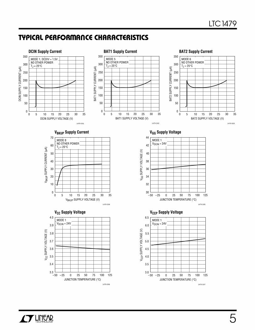
TYPICAL PERFORMANCE CHARACTERISTICS
UW
DCIN Supply Current BAT1 Supply Current BAT2 Supply Current
VGG Supply Voltage
JUNCTION TEMPERATURE (°C)–50
38
40
44
25 75
1479 G05
36
34
–25 0 50 100 125
32
30
42V G
G SU
PPLY
VOL
TAGE
(V)
MODE 1 VDCIN = 24V
VBKUP Supply Current
VBKUP SUPPLY VOLTAGE (V)0
40
50
70
15 25
1479 G04
30
20
5 10 20 30 35
10
0
60
V BKU
P SU
PPLY
CUR
RENT
(µA)
MODE 8 NO OTHER POWER TJ = 25°C
VCC Supply Voltage
JUNCTION TEMPERATURE (°C)–50
3.7
3.8
4.0
25 75
1479 G06
3.6
3.5
–25 0 50 100 125
3.4
3.3
3.9
V CC
SUPP
LY V
OLTA
GE (V
)
MODE 1 VDCIN = 24V
VCCP Supply Voltage
JUNCTION TEMPERATURE (°C)–50
5.0
5.5
6.5
25 75
1479 G07
4.5
4.0
–25 0 50 100 125
3.5
3.0
6.0
V CCP
SUP
PLY
VOLT
AGE
(V)
MODE 1 VDCIN = 24V
DCIN SUPPLY VOLTAGE (V)0
200
250
350
15 25
1479 G01
150
100
5 10 20 30 35
50
0
300
DCIN
SUP
PLY
CURR
ENT
(µA)
MODE 1, DCDIV = 1.5V NO OTHER POWER TJ = 25°C
BAT1 SUPPLY VOLTAGE (V)0
200
250
350
15 25
1479 G02
150
100
5 10 20 30 35
50
0
300
BAT1
SUP
PLY
CURR
ENT
(µA)
MODE 5 NO OTHER POWER TJ = 25°C
BAT2 SUPPLY VOLTAGE (V)0
200
250
350
15 25
1479 G03
150
100
5 10 20 30 35
50
0
300
BAT2
SUP
PLY
CURR
ENT
(µA)
MODE 6 NO OTHER POWER TJ = 25°C

6
LTC1479
PIN FUNCTIONS
UUU
External Power Supply Pins
DCIN (Pin 1): Supply Input. A 330Ω resistor should beput in series with this pin and the external DC powersource. A 0.1µF bypass capacitor should be connected tothis pin as close as possible.
DCDIV (Pin 2): Supply Divider Input. This is a highimpedance comparator input with a 1.215V threshold(rising edge) and approximately –35mV hysteresis.
BAT1, BAT2 (Pins 35, 34): Supply Input. These two pinsare the inputs from the two batteries. A 1µF bypasscapacitor should be connected to each pin as close aspossible if there is no larger battery supply capacitorwithin 2".
VBAT (Pin 32): Battery Voltage Sense. This pin connectsthe top of the battery resistor ladder to either BAT1 orBAT2.
BDIV (Pin 33): Battery Divider Input. A high impedancecomparator input with a 1.215V threshold (falling edge)and approximately 35mV hysteresis.
VBKUP (Pin 36): Supply Input. This input supplies power tothe LTC1479 when in the backup mode of operation. A 1µFbypass capacitor should be connected to the VBKUP pin asclose as possible if there is no larger backup supplycapacitor within 2".
Internal Power Supply Pins
VCCP (Pin 20): Power Supply Output. Bypass this outputwith at least a 0.1µF capacitor. The VCCP power supply isused primarily to power internal logic circuitry.
VCC (Pin 15): Power Supply Output. This is a nominal3.60V output. Bypass this regulator output with a 2.2µFtantalum capacitor. This capacitor is required for stability.
V+ (Pin 17): Supply. The V+ pin is connected via threeinternal diodes to the DCIN, BAT1 and BAT2 pins andpowers the top of the VGG switching regulator inductor.Bypass this pin with a 1µF/35V capacitor.
VGG (Pin 16): Gate Supply. This high voltage (36.5V)switching regulator is intended only for driving the internal
micropower gate drive circuitry. Do not load this pin withany external circuitry. Bypass this pin with a 1µF/50Vcapacitor.
SW (Pin 18): Output. This pin drives the “bottom” of theVGG switching regulator inductor which is connectedbetween this pin and the V + pin.
GND (Pin 19): Ground. The VGG and V + bypass capacitorsshould be returned to this ground which is connecteddirectly to the source of the N-channel switch in the VGGregulator.
Input Power Switches
GA, GB (Pins 4, 6): DCIN Switch Gate Drive. These twopins drive the gates of the back-to-back N-channel switchesin series with the DCIN input.
SAB (Pin 5): Source Return. The SAB pin is connected tothe sources of SW A and SW B. A small pull-down currentsource returns this node to 0V when the switches areturned off.
GC, GD (Pins 7, 9): BAT1 Switch Gate Drive. These twopins drive the gates of the back-to-back N-channelswitches in series with the BAT1 input.
SCD (Pin 8): Source Return. The SCD pin is connected tothe sources of SW C and SW D. A small pull-down currentsource returns this node to 0V when the switches areturned off.
GE, GF (Pins 10, 12): BAT2 Switch Gate Drive. These twopins drive the gates of the back-to-back N-channelswitches in series with the BAT2 input.
SEF (Pin 11): Source Return. The SEF pin is connected tothe sources of SW E and SW F. A small pull-down currentsource returns this node to 0V potential when the switchesare turned off.
SENSE+ (Pin 13): Inrush Current Input. This pin shouldbe connected directly to the “top” (switch side) of the lowvalued resistor in series with the three input powerselector switch pairs, SW A/B, SW C/D and SW E/F, fordetecting and controlling the inrush current into and outof the power supply sources and the output capacitor.

7
LTC1479
PIN FUNCTIONS
UUU
SENSE – (Pin 14): Inrush Current Input. This pin shouldbe connected directly to the “bottom” (output side) of thelow valued resistor in series with the three input powerselector switch pairs, SW A/B, SW C/D and SW E/F, fordetecting and controlling the inrush current into and outof the power supply sources and the output capacitor.
Battery Charging Switches
GG, GH (Pins 29, 27): Charger Switch Gate Drive. Thesetwo pins drive the gates of the back-to-back N-channelswitch pairs, SW G and SW H, between the charger outputand the two batteries.
SG, SH (Pin 28, 26): Source Returns. These two pins areconnected to the sources of SW G and SW H respectively.A small pull-down current source returns these nodes to0V when the switches are turned off.
CHGMON (Pin 31): Battery Selector Output. This pin isthe output of an internal switch which is connected toBAT1 and BAT2 and connects the positive terminal of theselected battery to the voltage feedback resistors in thecharger circuit.
Microprocessor Interface
DCINGOOD (Pin 25): Comparator Output. This open-drainoutput has an internal 2µA pull-up current source con-nected through a diode to the VCCP power supply. Anexternal pull-up resistor can be added if more pull-upcurrent is required. This output is active high when the DCsupply rises above the programmed voltage.
LOBAT (Pin 3): Comparator Output. This open-drain out-put does not have an internal pull-up current source andis active low when the selected battery voltage dropsbelow the programmed voltage.
DCIN/BAT (Pin 24): Selector Input. This high impedancelogic input allows the µP to make the ultimate decision onthe connection of the DC power source, based upon theDCINGOOD pin information. In some minimized systems,the DCIN/BAT pin may be connected directly to theDCINGOOD pin.
BATDIS (Pin 23): Battery Disconnect Input. This high-impedance logic input has a built-in 2µA pull-up currentsource and allows the µP to disconnect the battery fromthe system.
3DM (Pin 22): Three Diode Mode Input. This high imped-ance logic input has no built-in pull-up current source.Connect a 100k resistor from this pin to ground to ensurethree diode mode operation from a “cold start.”
CHGSEL (Pin 21): Battery Charger Selector Input. Thishigh impedance logic input has a built-in 2µA pull-upcurrent source and allows the µP to determine whichbattery is being charged by connecting the selectedbattery to the charger output via one of the switch pairs,SW G or SW H. (The charger voltage feedback ladder issimultaneously switched to the selected battery.)
BATSEL (Pin 30): Battery Selector Input. This high imped-ance logic input has a built-in 2µA pull-up current sourceand allows the µP to select which battery is connected tothe system and the battery monitor comparator input.Battery 1 is selected with a logic high on this input andbattery 2 is selected with a logic low.

8
LTC1479
BLOCK DIAGRAM
W
DCDIV
GA GBSAB VSENSE+ VSENSE –
BAT2 INRUSH SENSE
BAT1 INRUSH SENSE
DCIN INRUSH SENSE
GC GDSCD GE GFSEF
BAT1 BAT2 DCIN
V+
SW
VCC
VGG
BAT1 BAT2 DCIN
BDIV
BAT2
BAT1
VBAT CHGMONBATSEL CHGSEL
SW G GATE
DRIVER
SG GG
SW H GATE
DRIVER
SH GH
VCCP
DCINGOOD
LOBAT
GND
DCIN
3DM
DCIN/BAT
2µA
VCCP
BATDIS
2µA
VCCP
VCCP2µA
VCCP 2µA
VCCP
1479 BD
DCIN MONITOR
SW A/B GATE
DRIVERS
SW C/D GATE
DRIVERS
SW E/F GATE
DRIVERS
VCC REGULATOR
& BIAS GENERATOR
VGG SWITCHING REGULATOR
BATTERY MONITOR
SWITCH CONTROL
LOGIC
VBKUP
9
LTC1479
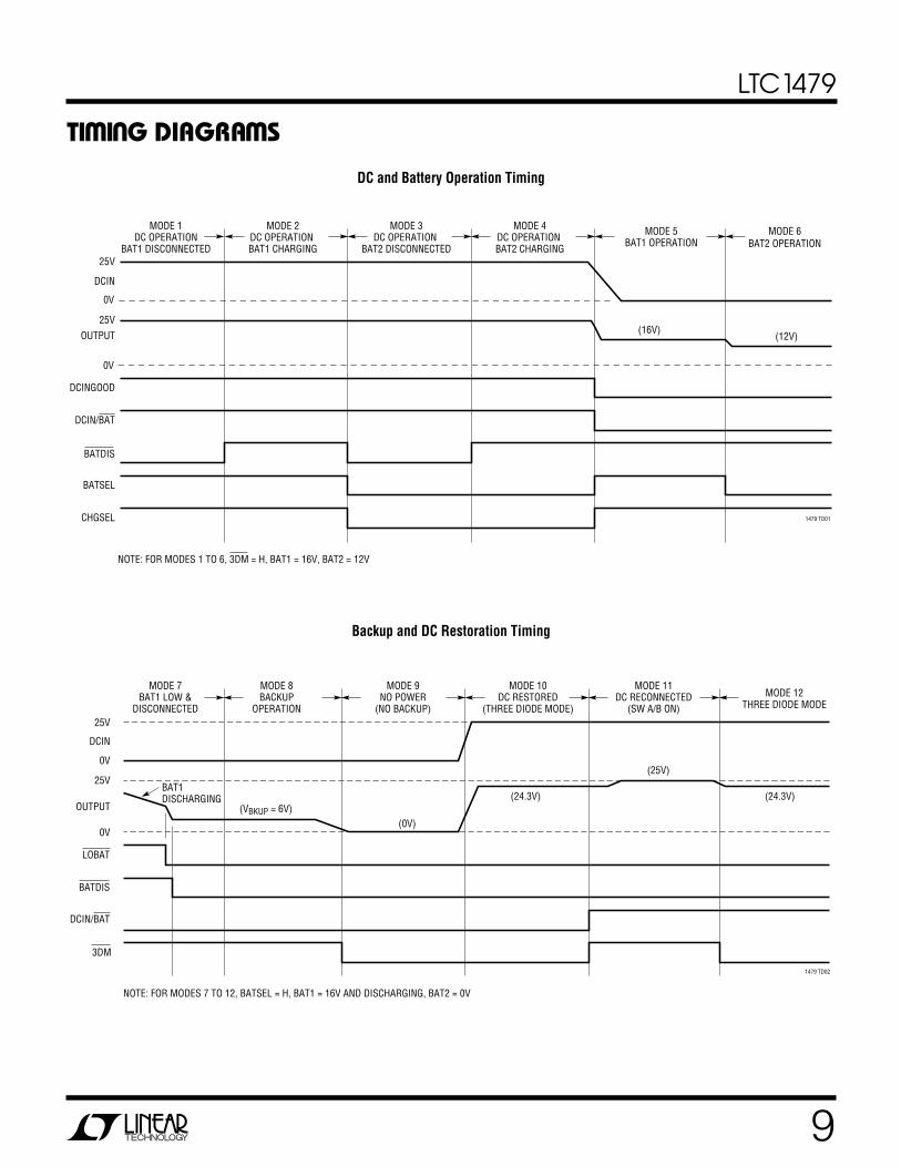
TI I G DIAGRA SW WU
DC and Battery Operation Timing
DCIN
DCINGOOD
DCIN/BAT
BATSEL
MODE 1 DC OPERATION
BAT1 DISCONNECTED
MODE 2 DC OPERATION BAT1 CHARGING
CHGSEL
MODE 3 DC OPERATION
BAT2 DISCONNECTED
MODE 4 DC OPERATION BAT2 CHARGING
BATDIS
MODE 5 BAT1 OPERATION
MODE 6 BAT2 OPERATION
NOTE: FOR MODES 1 TO 6, 3DM = H, BAT1 = 16V, BAT2 = 12V
25V
25V(16V)
(12V)
1479 TD01
0V
OUTPUT
0V
Backup and DC Restoration Timing
DCIN
MODE 7 BAT1 LOW &
DISCONNECTED
MODE 8 BACKUP
OPERATION
MODE 9 NO POWER
(NO BACKUP)
MODE 10 DC RESTORED
(THREE DIODE MODE)
BATDIS
MODE 11 DC RECONNECTED
(SW A/B ON)
MODE 12 THREE DIODE MODE
NOTE: FOR MODES 7 TO 12, BATSEL = H, BAT1 = 16V AND DISCHARGING, BAT2 = 0V
25V
25V
0V
OUTPUT
0V
DCIN/BAT
3DM
LOBAT
BAT1 DISCHARGING
(VBKUP = 6V)(0V)
(24.3V) (24.3V)
1479 TD02
(25V)

10
LTC1479
OPERATIONU
The LTC1479 is responsible for low-loss switching at the“front end” of the power management system, where upto two battery packs and a DC power source can beindiscriminately connected and disconnected. Smoothswitching between input power sources is accomplishedwith the help of low-loss N-channel switches driven byspecial gate drive circuitry which limits the inrush currentin and out of the battery packs and the system powersupply capacitors.
All N-Channel Switching
The LTC1479 drives external back-to-back N-channelMOSFET switches to direct power from the three mainpower sources: the external DC power source, the pri-mary battery and the secondary battery connected to themain supply pins—DCIN, BAT1 and BAT2 respectively.(N-channel MOSFET switches are more cost effectiveand provide lower voltage drops than their P-channelcounterparts.)
Gate Drive (VGG) Power Supply
The gate drive for the low-loss N-channel switches issupplied by a micropower boost regulator which is regu-lated at approximately 36.5V. The VGG supply providessufficient headroom above the maximum 28V operatingvoltage of the three main power sources to ensure that theMOSFET switches are fully enhanced.
The power for this inductor based regulator is taken fromthree internal diodes as shown in Figure 1. The three
Figure 1. VGG Switching Regulator
BAT1 BAT2DCIN
V+
SW
GND1479 F01
VGG
+ +
L1 1mH
C1 1µF 35V
C2 1µF 50V
TO GATE DRIVERS
(36.5V)
LTC1479
VGG SWITCHING REGULATOR
diodes are connected to each of the three main powersources, DCIN, BAT1 and BAT2. The highest voltagepotential is directed to the top of the boost regulatorinductor to maximize regulator efficiency. C1 providesfiltering at the top of the 1mH switched inductor, L1, whichis housed in a small surface mount package.
A fourth internal diode directs the current from the 1mHinductor to the VGG output capacitor, C2, further reducingthe external parts count. In fact, as demonstrated in Figure1, only three external components are required by the VGGregulator, L1, C1 and C2.
Inrush Current Limiting
The LTC1479 uses an adaptive inrush current limitingscheme to reduce current flowing in and out of the threemain power sources and the DC/DC converter input ca-pacitor during switch-over transitions. The voltage acrossa single small-valued resistor, RSENSE, is measured toascertain the instantaneous current flowing through thethree main switch pairs, SW A/B, SW C/D, and SW E/Fduring the transitions.
Figure 2 is a block diagram showing only the DCIN switchpair, SW A/B. (The gate drive circuits for switch pairs SWC/D and SW E/F are identical). A bidirectional currentsensing and limiting circuit determines when the voltagedrop across RSENSE reaches plus or minus 200mV. Thegate-to-source voltage, VGS, of the appropriate switch islimited during the transition period until the inrush currentsubsides, generally within a few milliseconds, dependingupon the value of the DC/DC converter input capacitor.
VSENSE+ VSENSE–GA GBSAB
SW A SW B RSENSE
VGG
LTC1479
1479 F02
DCIN
+
OUTPUT TO DC/DC CONVERTER
COUT
6V 6V±200mV
THRESHOLD
SW A/B GATE
DRIVERS
BIDIRECTIONAL INRUSH CURRENT
SENSING AND LIMITING
Figure 2. SW A/B Inrush Current Limiting

11
LTC1479
OPERATIONU
This scheme allows capacitors and MOSFET switches ofdiffering sizes and current ratings to be used in the samesystem without circuit modifications.
After the transition period has passed, the VGS of bothMOSFETs in the selected switch pair rises to approxi-mately 6V. The gate drive is set at 6V to provide ampleoverdrive for logic level MOSFET switches without ex-ceeding their maximum VGS rating.
Internal Power Supplies
Two internal supplies provide power for the control logicand power source monitoring functions. The VCCP logicsupply is approximately 5V and provides power for themajority of the internal logic circuitry. The VCC supply isapproximately 3.60V and provides power for the VGGswitching regulator control circuitry and the gate drivers.
The VCC supply has an undervoltage lockout circuit whichminimizes power consumption in the event of a total lossof system power; i.e., when all available power sources fallbelow approximately 4.5V.
DCIN Voltage Monitoring
The DCIN input is continuously monitored via a tworesistor ladder connected between the DCIN pin and theDCDIV input. The input threshold is 1.215V (rising edge)with approximately –35mV hysteresis. The use of a defini-tive voltage threshold ensures that the DC supply is notonly connected but “healthy” before being attached to theDC/DC converter input.
Battery Voltage Monitoring
The LTC1479 has the ability to independently monitor bothbattery packs. (Because of this, one battery pack may bedischarged as the other is being charged.)
A low-battery detector signals when the selected batterypack has dropped to the level where a shutdown sequenceshould be initiated or the other battery pack engaged.
Battery Charging Management Functions
The LTC1479 directly interfaces with LT1510/LT1511battery charger circuits. Two gate drive circuits controlthe two back-to-back N-channel switch pairs, SW G andSW H, under logic (CHGSEL) control to connect theoutput of the charger to the selected battery pack. Break-before-make action ensures that current does not passfrom one battery pack to the other during switch-over ofthe charger output. The CHGSEL input also simulta-neously switches the positive terminal of the selectedbattery pack to the top of the voltage feedback resistorladder in the charger system through the CHGMON pin.
Backup Supply Interface
Power for the LTC1479 is obtained from the backupsupply when power is unavailable from the three mainsources of power.
Interface to Companion Microprocessor
A companion µP must be used in conjunction with theLTC1479 to provide overall control of the power manage-ment system. The LTC1479 communicates with the µP bymeans of five logic inputs and two logic outputs asdescribed in Table 1.
Table 1. LTC1479 µP Interface Inputs and Outputs
INPUT ACTION
DCIN/BAT Logic High Required to Connect a Good DC Supply
BATDIS Logic Low Disconnects the Battery from the System
BATSEL Selects Which Battery is Connected to the System(Logic High Selects BAT1; Logic Low Selects BAT2)
CHGSEL Selects Which Battery is Charged and Monitored(Logic High Selects BAT1; Logic Low Selects BAT2)
3DM Forces the Main Three Power Path Switches Into“3-Diode Mode.” See Applications Information Section
OUTPUT ACTION
DCINGOOD Logic High When a Good DC Supply is Present
LOBAT Logic Low When Selected Battery Voltage is Low

12
LTC1479
APPLICATIONS INFORMATION
WU UU
POWER PATH SWITCHING CONCEPTS
Power Source Selection
The LTC1479 drives low-loss switches to direct power inthe main power path of a dual rechargeable battery system— the type found in most notebook computers and otherportable equipment.
Figure 3 is a conceptual block diagram which illustratesthe main features of an LTC1479 dual battery powermanagement system, starting with the three main powersources and ending at the system DC/DC regulator.
Switches SW A/B, SW C/D and SW E/F direct power fromeither the AC adapter (DCIN) or one of the two batterypacks (BAT1 and BAT2) to the input of the DC/DC switch-ing regulator. Switches SW G and SW H connect thedesired battery pack to the battery charger.
Each of the five switches is intelligently controlled by theLTC1479 which interfaces directly with a power manage-ment system µP.
Using Tantalum Capacitors
The inrush and “outrush” current of the system DC/DCregulator input capacitor is limited by the LTC1479. i.e.,the current flowing both in and out of the capacitor duringtransitions from one input power source to another islimited. In many applications, this inrush current limitingmakes it feasible to use lower cost/size tantalum surfacemount capacitors in place of more expensive/larger alumi-num electrolytics at the input of the DC/DC converter.
Note: The capacitor manufacturer should be consulted forspecific inrush current specifications and limitations andsome experimentation may be required to ensure compli-ance with these limitations under all possible operatingconditions.
Back-to-Back Switch Topology
The simple SPST switches shown in Figure 3 actuallyconsist of two back-to-back N-channel switches. Theselow-loss, N-channel switch pairs are housed in 8-pin SOand SSOP packaging and are available from a number ofmanufacturers. The back-to-back topology eliminates theproblems associated with the inherent body diodes inpower MOSFET switches and allows each switch pair toblock current flow in either direction when the two switchesare turned off.
The back-to-back topology also allows for independentcontrol of each half of the switch pair which facilitatesbidirectional inrush current limiting and the so called “3-diode” mode described in the following section.
The “3-Diode” Mode
Under normal operating conditions, both halves of eachswitch pair are turned on and off simultaneously. Forexample, when the input power source is switched from agood DC input (AC adapter) to a good battery pack, BAT1,both gates of switch pair SW A/B are turned off and bothgates of switch pair SW C/D are turned on. The back-to-back body diodes in switch pair, SW A/B, block currentflow in or out of the DC input connector.
Figure 3. LTC1479 PowerPath Conceptual Diagram
BAT1
BAT2
SW A/B
SW C/D
SW E/F
SW G SW H
+ HIGH EFFICIENCY
DC/DC SWITCHING REGULATOR
5V
3.3V
12V
CIN
RSENSE
DCIN
1479 F03
POWER MANAGEMENT
µP
LTC1479 PowerPath CONTROLLER
BATTERY CHARGER

13
LTC1479
APPLICATIONS INFORMATION
WU UU
the Power Management µP Interface section for additionalinformation on when to invoke “3-diode” mode.)
COMPONENT SELECTION
N-Channel SwitchesThe LTC1479 adaptive inrush limiting circuitry permits theuse of a wide range of logic-level N-channel MOSFETswitches. A number of dual low RDS(ON) N-channel switchesin 8-lead surface mount packages are available that arewell suited for LTC1479 applications.The maximum allowable drain source voltage, VDS(MAX),of the three main switch pairs, SW A/B, SW C/D and SWE/F, must be high enough to withstand the maximum DCsupply voltage. If the DC supply is in the 20V to 28V range,use 30V MOSFET switches. If the DC supply is in the 10Vto 18V range, and is well regulated, then use 20V MOSFETswitches.
As a general rule, select the switch with the lowest RDS(ON)at the maximum allowable VDS. This will minimize the heatdissipated in the switches while increasing the overallsystem efficiency. Higher switch resistances can be toler-ated in some systems with lower current requirements,but care should be taken to ensure that the power dissi-pated in the switches is never allowed to rise above themanufacturer’s recommended levels.
The maximum allowable drain-source voltage, VDS(MAX),of the two charger switch pairs, SW G and SW H, need only
Figure 4. LTC1479 PowerPath Switches in “3-Diode” Mode
BAT1
BAT2
SW A
SW C
SW E
+HIGH
EFFICIENCY DC/DC
SWITCHING REGULATOR
5V
3.3V
12V
CIN
DCIN
1479 F04
SW B
SW F
SW D
RSENSE
POWER MANAGEMENT
µP
LTC1479 PowerPath CONTROLLER
ON OFF
ON OFF
ON OFF
In the “3-diode” mode, only the first half of each powerpath switch pair, i.e., SW A, SW C and SW E, is turned on;and the second half, i.e., SW B, SW D and SW F, is turnedoff. These three switch pairs now act simply as threediodes connected to the three main input power sourcesas illustrated in Figure 4. The power ‘diode’ with thehighest input voltage passes current through to the inputof the DC/DC converter to ensure that the power manage-ment µP is powered at start-up or under abnormal oper-ating conditions. (An undervoltage lockout circuit defeatsthis mode when the V + pin drops below approximately4.5V).
“Cold Start” Initial ConditionThe LTC1479 is designed to start in the “3- diode” modewhen all five logic inputs are low—when no power isavailable (including the backup system). A 100k resistorfrom the 3DM input to ground ensures that this input is lowduring a “cold start.” This will cause the main PowerPathswitches to pass the highest voltage available to the inputof the DC/DC converter. Normal operation will thenresume after a good power source is identified.
Recovery from Uncertain Power ConditionsThe “3-diode” mode can also be asserted (by applying anactive low to the 3DM input) when abnormal conditionsexist in the system, i.e., when all power sources aredeemed not “good” or are depleted, or the managementsystem µP is being reset or not functioning properly. (See

14
LTC1479
be high enough to withstand the maximum battery orcharger output voltage. In most cases, this will allow theuse of 20V MOSFET switches in the charger path, while30V switches are used in the main power path.
Inrush Current Sense Resistor, RSENSE
A small valued sense resistor (current shunt) is used bythe three main switch pair drivers to measure and limit theinrush current flowing through the conducting switchpair.
It should be noted that the inrush limiting circuit is notintended to provide short-circuit protection ; but rather, isdesigned to limit the large peak currents which flow into orout of the large power supply capacitors and the batterypacks during power supply switch-over transitions. Theinrush current limit should be set at approximately 2× or3× the maximum required DC/DC input current.
For example, if the maximum current required by theDC/DC converter is 2A, an inrush current limit of 6A is setby selecting a 0.033Ω sense resistor, RSENSE, using thefollowing formula:
RSENSE = (200mV)/IINRUSH
Note that the voltage drop across the resistor in thisexample is only 66mV under normal operating conditions.Therefore, the power dissipated in the resistor is extremelysmall (132mW), and a small 1/4W surface mount resistorcan be used in this application. A number of small valued,surface mount resistors are available that have beenspecifically designed for high efficiency current sensingapplications.
DC Input Monitor Resistor Divider
The DCDIV input continuously monitors the DC powersupply voltage via a two resistor divider network, RDC1 andRDC2, as shown in Figure 5. The threshold voltage of theDC good comparator is 1.215V when the power supplyinput voltage is rising. Approximately –35mV of hyster-esis is provided to ensure clean switching of the compara-tor when the DC supply voltage is falling.
To minimize errors due to the input bias current of the DCgood comparator, set RDC1 = 12.1k so that approximately100µA flows through the resistor divider when the desired
APPLICATIONS INFORMATION
WU UU
Figure 5. DC Monitor Resistor Divider
LTC1479DCIN
DCDIV
DC SUPPLY
TO SW A/B
RDC1 12.1k
1%
RDC2 1%
1.215VDCINGOOD
1479 F05
–
+
BATSEL
BAT1
BAT2
LOBAT
LTC1479
1479 F06
1.215V
VBAT
BDIV
RB1 121k 1%
RB2 1%
–
+
SWITCH CONTROL
LOGIC
threshold is reached. RDC2 is then selected according tothe following formula:
RDC2 = 12.1k – 1VGOOD 1.215V ))
Battery Monitor Resistor Divider
A switch controlled by the BATSEL input connects one ofthe two batteries to the VBAT pin and therefore to the topof the battery resistor divider as shown in Figure 6. Thethreshold voltage of the low-battery comparator is 1.215Vwhen the battery voltage is falling. Approximately +35mVof hysteresis is provided to ensure clean switching of thecomparator when the battery voltage rises again.
To minimize errors due to the input bias current of the lowbattery comparator, assume RB1 = 121k so that approxi-mately 10µA flows through the resistor divider when thethreshold is reached. RB2 is selected according to thefollowing formula:
Figure 6. Battery Monitor Resistor Divider

15
LTC1479
APPLICATIONS INFORMATION
WU UU
RB2 = 121k – 1VLOBAT 1.215V ))
VGG Regulator Inductor and Capacitors
The VGG regulator provides a power supply voltage signifi-cantly higher than any of the three main power sourcevoltages to allow the control of N-channel MOSFETswitches. This 36.5V micropower, step-up voltage regula-tor is powered by the highest potential available from thethree main power sources for maximum regulator effi-ciency.
Because the three input supply diodes and regulatoroutput diode are built into the LTC1479, only three externalcomponents are required by the VGG regulator: L1, C1 andC2 as shown in Figure 7.
L1 is a small, low current 1mH surface mount inductor. C1provides filtering at the top of the 1mH switched inductorand should be 1µF to filter switching transients. The VGGoutput capacitor, C2, provides storage and filtering for theVGG output and should be 1µF and rated for 50V operation.C1 and C2 can be either tantalum or ceramic capacitors.
VCC and VCCP Regulator Capacitors
The VCCP logic supply is approximately 5V and providespower for the majority of the internal logic circuitry.Bypass this output with a 0.1µF capacitor.
The VCC supply is approximately 3.60V and providespower for the VGG switching regulator control circuitry andthe gate drivers. Bypass this output with a 2.2µF tantalumcapacitor. This capacitor is required for stability of the VCCregulator output.
SYSTEM LEVEL CONSIDERATIONS
The Complete Power Management SystemThe LTC1479 is the “heart” of a complete power manage-ment system and is responsible for the main power pathand charger switching. A companion power managementµP provides overall control of the power managementsystem in concert with the LTC1479 and the auxiliarypower management systems.
A typical dual Li-Ion battery power management system isillustrated in Figure 8. If “good” power is available at theDCIN input (from the AC adapter), switch pair SW A/B areturned on—providing a low-loss path for current flow tothe input of the LTC1538-AUX DC/DC converter. Switchpairs, SW C/D and SW E/F are turned off to block currentfrom flowing back into the two battery packs from the DCinput.
In this case, an LT1510 constant-voltage/constant-cur-rent (CC/CV) battery charger circuit is used to alternatelycharge the two Li-Ion battery packs. The µP “decides”which battery is in need of recharging by either queryingthe “smart” battery directly or by more indirect means.After the determination is made, either switch pair, SW Gor SW H, is turned on to pass charger output current to oneof the batteries. Simultaneously, the selected battery volt-age is returned to the voltage feedback input of the LT1510CV/CC battery charger via the CHGMON output of theLTC1479. After the first battery has been charged, it isdisconnected from the charger circuit and the secondbattery is connected through the other switch pair and thesecond battery charged.
Backup power is provided by the LT1304 circuit whichensures that the DC/DC input voltage does not dropbelow 6V.
Backup System InterfaceThe LTC1479 is designed to work in concert with relatedpower management products including the LT1304 mi-Figure 7. VGG Step-Up Switch Regulator
BAT1 BAT2DCIN
V+
SW
GND
*COILCRAFT 1812LS-105 XKBC (708) 639-6400 OR EQUIVALENT
1479 F07
VGG
+ +
L1* 1mH
C1 1µF 35V
C2 1µF 50V
TO GATE DRIVERS
(36.5V)
LTC1479
VGG SWITCHING REGULATOR

16
LTC1479
APPLICATIONS INFORMATION
WU UU
DCIN
DCIN
BAT1
BAT2
+ +
V+ SW VGG
1µF 50V
1µF 50V
1mH*
VCC
+
RSENSE 0.033ΩSW A SW B
SW C SW D
SW E SW F
GA
330Ω
GB GC GD GE GFSAB SCD SEF SENSE+ SENSE–
2
5
+
VCCP
2.2µF 16V
0.1µF
VBAT POWER MANAGEMENT
µPBDIV
VBKUPBACKUP
REGULATOR
LTC1538-AUX TRIPLE, HIGH EFFICIENCY, SWITCHING REGULATOR
DCDIV
0.1µF
LTC1479
LT1510 Li-ION BATTERY
CHARGER
GG SG GH SH
CHGMON
3.3V
5V
SW G
SW H
DCIN
Li-ION BATTERY PACK #1
Li-ION BATTERY PACK #2
1479 F08
BACKUP NiCD
*COILCRAFT 1812LS-105 XKBC (708) 639-1469
12V AUX
RB2
RB1
RDC2
RDC1
cropower DC/DC converter. As shown in Figure 9, theLT1304 monitors the input supply voltage and activateswhen it drops below 6V.
Power for the DCIN and battery monitors and the logicsupply in the LTC1479 is then obtained from the output ofthe LT1304 step-up regulator.
Charger System Interface
The LTC1479 is designed to work directly with constant-voltage (CV), constant-current (CC) battery chargers suchas the LT1510 and LT1511.
LT1510 Battery Charger Interface
As illustrated in Figure 10, the LT1510 CV/CC batterycharger, takes power from the DC adapter input throughSchottky diode D1. The output of the charger is directed to
FROM PowerPath
CONTROLLER
BACKUP
NiCD CELL
TO INPUT OF DC/DC CONVERTER L1*
10µH
(BOLD LINES INDICATE HIGH CURRENT PATHS)
5VCC FROM DC/DC
D1 MBR0530
R4 390k 1%
R5 100k 1%
SW
+
FB
SHDN
VINGND
LT1304
C1 0.1µF
C3 0.1µF
ILIM
R3 22k
LBI
R2 470k
4
8
7
3
5
1479 F09
C2 0.1µF
1
6
2LBO
5VCC FROM DC/DC
D2 BAS16LT1
Q1 2N7002
ROHM DTA144E R1
10k
Figure 9. LT1304 Micropower Backup Converter Circuit
Figure 8. Simplified Dual Li-Ion Battery Power Management System

17
LTC1479
APPLICATIONS INFORMATION
WU UU
the charging battery through one of the N-channel switchpairs, SW G or SW H. The charging battery voltage issimultaneously connected through the CHGMON switchin the LTC1479 to the top of the charger voltage resistordivider, R4 and R5, for constant voltage charging. (See theLT1510 data sheet for further detail.)
LT1511 Battery Charger Interface
The LT1511, 3A CC/CV battery charger with input currentlimiting, is connected in a slightly different manner thanthe LT1510 as illustrated in Figure 11.
Figure 11. Interfacing to the LT1511 Constant-Voltage/Constant-Current Battery Charger with Input Current Limiting
1479 F11
SW H Si9926DY
SW G Si9926DY
BAT1 4 Li-ION
BATTERY PACK
BAT2 4 Li-ION
BATTERY PACK
+
+CBAT1 47µF
CBAT2 47µF
DC INPUT (FROM AC ADAPTOR)
VCC
D1 MBRS340T
R1 500Ω
C2 0.33µF
C1 1µF
PROG
RPROG 4.93k 1%
RS4 0.05Ω
C3 200pF
VC SWUV
BOOSTCOMP1
SPIN
BAT SENSEGND
C6 0.47µF
C7 50pF
C12 1µFC5
10µF
D3 MBR0540T
L1 20µH
D2 MBRS340T
LT1511
C4 10µF CERAMIC
0.1µF
330Ω
+ CCHG 22µF TANT
+
(CHARGER OUTPUT)
Q1 2N7002
R2 1k
CURRENT CONTROL FROM POWER
MANAGEMENT µP
+
–R6
649k 0.25%
R5 6.8k
R4 5k
R3 500Ω
R7 115k
0.25%RS3 200Ω 1%
RS2 200Ω
1% RS1 0.033Ω
OVP
CLPCLN
TO SW C/DTO SW E/F TO
SW A/B
+
–
POWER MANAGEMENT
µPBAT1 BAT2 GG SG GH SH
CHGMON
DCINLTC1479
1479 F10
SW H Si9926DY
SW G Si9926DY
BAT1 4 Li-ION
BATTERY PACK
BAT2 4 Li-ION
BATTERY PACK
+
+CBAT1 47µF
CBAT2 47µF
DC INPUT (FROM AC ADAPTOR)
VCC
D1 MBRS140T
R2 300Ω
C1 1µF
PROG
RPROG 11k 1%
R3 1k
C2 0.1µF
VC
SW
BOOST
SENSE
BATGND
C3 0.22µF
0.1µF
D3 1N4148
L1* 33µH
D2 MBRS140T
LT1510
C6 10µF
CERAMIC
+ CCHG 22µF TANT
(CHARGER OUTPUT)
Q1 2N7002
R1 100k 1%
CURRENT CONTROL FROM POWER
MANAGEMENT µP
+
–R4
649k 0.25%
R5 115k
0.25%
OVP
*COILTRONICS CTX33-2
TO SW C/D
TO SW E/F
TO SW A/B
330Ω
+
–
POWER MANAGEMENT
µPBAT1 BAT2 GG SG GH SH
CHGMON
DCIN
LTC1479
Figure 10. Interfacing to the LT1510 Constant-Voltage/Constant-Current Battery Charger

18
LTC1479
APPLICATIONS INFORMATION
WU UU
The LT1511 has a third control loop that regulates thecurrent drawn from the AC adapter. Therefore, the DCinput to the LTC1479 and the input to the host systemthrough SW A/B, is obtained from the “output” of theLT1511 adapter sense resistor, RS4, and not directly fromthe DC input connector as with the LT1510. This allowssimultaneous operation of the host system while charginga battery without overloading the AC adapter. Chargingcurrent is reduced to keep the adapter current withinspecified levels.
However, as with the LT1510 , the output of the LT1511 isdirected to the charging battery through either SW G or SWH, and the charging battery voltage is connected to the topof the voltage resistor divider, R6 and R7, for constantvoltage charging. (See the LT1511 data sheet for furtherdetail on battery charging techniques and applicationshints.)
LT1620/LTC1435 Battery Charger Interface
The LTC1479 also interfaces with the LT1620/LTC1435synchronous high efficiency low dropout battery charger.The circuit shown in Figure 12 is a constant-current/constant-voltage battery charger specifically designed forlithium-ion applications having thermal, output current, orinput voltage headroom constraints which preclude theuse of other high performance chargers such as theLT1510 or LT1511.
This circuit can charge batteries at up to 4A. The precisioncurrent sensing of the LT1620 combined with the highefficiency and low dropout characteristics of the LTC1435provide a battery charger with over 96% efficiency requir-ing only 0.5V input-to-output differential at 3A chargingcurrent.
Charge current programming is achieved by applying a0µA to 100µA current from the LT1620 PROG pin toground, which can be derived from a resistor or DACoutput controlled by the power management µP. (See theLT1620 data sheet for further details on this circuit.)
Capacitive Loading on the CHGMON Output
In most applications, there is virtually no capacitive load-ing on the CHGMON output—just a simple resistordivider. Care should be taken to restrict the amount of
capacitance to ground on the CHGMON output to less than100pF. If more capacitance is required, it may becomenecessary to “mask” the LOBAT output when the chargemonitor is switched between batteries. (Internal resis-tance between the BAT1 and BAT2 inputs and the chargemonitor switch may create a transient voltage drop at theVBAT output during transitions which could be falselyinterpreted by the µP as a low battery condition.)
THE POWER MANAGEMENT MICROPROCESSOR
Interfacing to the LTC1479
The LTC1479 can be thought as a “real world” interface tothe power management µP. It takes logic level commandsdirectly from the µP, and makes changes at high currentand high voltage levels in the power path. Further, itprovides information directly to the µP on the status of theAC adapter, the batteries and the charging system.
The LTC1479 logic inputs are TTL level compatible andtherefore interface directly with standard power manage-ment µPs. Further, because of the direct interface via thefive logic inputs and the two logic outputs, there is virtuallyno latency (i.e. time delay) between the µP and the LTC1479.In this way, time critical decisions can be made by the µPwithout the inherent delays associated with bus protocols,etc. These delays are acceptable in certain portions of thepower management system, but it is vital that the powerpath switching control be made through a direct connec-tion to the power management µP. The remainder of thepower management system can be easily interfaced to theµP through a serial interface.
Selecting a Power Management Microprocessor
The power management µP provides intelligence for theentire power system, is programmed to accommodate thecustom requirements of each individual system and allowperformance updates without resorting to costly hard-ware changes.
The power management µP must meet the requirementsof the total power management system, including theLTC1479 controller, the batteries (and interface), thebackup system, the charging system and the host proces-sor. A number of inexpensive processors are availablewhich can easily fulfill these requirements.

19
LTC1479
APPLICATIONS INFORMATION
WU UU
1
2
3
4
5
6
7
8 9
10
11
12
13
14
15
16COSC
RUN/SS
ITH
SFB
SGND
VOSENSE
SENSE+
SENSE–
TG
BOOST
SW
VIN
INTVCC
BG
PGND
VCC
LTC1435 +
1
2
3
4 5
6
7
8SENSE
IOUT
GND
NIN PIN
VCC
PROG
AVG
LT1620+
SHDN
IPROG
DC INPUT (FROM AC ADAPTER)
TO W A/B
330Ω
+
R1 1M 0.1%
R2 76.8k 0.1%
C1 100pF
0.1µF
C2 100pF
C3 0.1µF
R5 1.5M
R5, 1k
C4 0.033µF
C6 0.1µF
C5 0.01µF
C8 0.1µF
C9, 100pF
C10 100pF
C7 0.33µF
R3 10k 1%
C11 56pF
C12 0.1µF
D1* CMDSH-3
C13 0.33µF
D2* CMDSH-3
Q1 Si4412DY
Q2 Si4412DY
L1 27µH
C15 22µF 35V ×2
R4 0.025Ω
C14 4.7µF
C16 22µF 35V
1479 F12
SW H Si9926DY
SW G Si9926DY
BAT1 4 Li-ION
BATTERY PACK
BAT2 4 Li-ION
BATTERY PACK
+
+CBAT1 10µF
CBAT2 10µF
+
–
TO SW C/DTO SW E/F
+
–
POWER MANAGEMENT
µPBAT1 BAT2 GG SG GH SH
CHGMON
DCIN
LTC1479
*CENTRAL SEMICONDUCTOR CO. (516) 435-1110
Figure 12. Interfacing to an LT1620/LTC1435 High Efficiency Constant-Voltage/Constant-Current Battery Charger

20
LTC1479
APPLICATIONS INFORMATION
WU UU
Interfacing to the Battery Pack
The LTC1479 is designed to work with virtually anybattery pack chemistry or cell count, as long as thebattery pack operating voltage range is somewherebetween 6V and 28V. This permits great flexibility insystem design. The low-battery threshold is adjustableand can be set anywhere between 6V and 28V.
Conventional Battery Packs
Conventional battery packs do not include a “smart”battery interface between the battery pack and the hostsystem. Thus, these battery packs generally have onlythree terminals to connect the battery and a temperaturesensor (thermistor) to the host system. The NTC ther-mistor typically has a nominal resistance of 10k at roomtemperature and is used to monitor the battery packtemperature.
LOBAT and DCINGOOD Blanking/Filtering
It is good practice to include some delay in accepting lowbattery and DCIN good information during transitionalperiods, e.g., when switching the charger from one battery
to another or when switching from batteries to DC power.This technique will eliminate false triggering at the asso-ciated µP I/O. (Remember that the “3-diode” mode may beused during periods of uncertainty to eliminate the needfor “instantaneous” DCIN and battery status information.)
Smart Battery Packs
Smart battery packs, compliant with the Smart BatterySystem specification, have a five-terminal connector. Twoof the terminals are the minus and plus connections to thebattery. A third terminal is connected to the top of athermistor in NiCd and NiMH battery packs and to aresistor in Li-Ion battery packs. A fourth and fifth terminalare connected to the Smart Management Bus (SMBus)SMBDATA and SMBCLK lines from an integrated circuitinside the battery pack.
Applications Assistance
Linear Technology applications engineers have developeda smart battery charger around the LT1511 charger IC.Contact the factory for applications assistance in develop-ing a complete smart battery system with intelligentPowerPath control using the LTC1479.

21
LTC1479
TYPICAL APPLICATIONS N
U
Dual NiMH Battery Power Management System (Using an LT1510, 1A Charger)
1479 TA02
DCIN
BAT1
BAT2
+ +
V+ SW VGG
C3 1µF 50V
L1* 1mH
C4 1µF 50V
VCC
RSENSE 0.033ΩSW A SW B
SW C SW D
SW E SW F
GA GB GC GD GE GFSAB SCD SEF SENSE+ SENSE–
VCCP
C2 2.2µF 16V
C1 0.1µF
VBAT
POWER MANAGEMENT
µP
BDIV
VBKUPDCDIV
LTC1479
GG SG GH SH
NiCD CELL
1812LS-105 XKBC, COILCRAFT CD43, SUMIDA CTX33-2, COILTRONICS
* **
***
RB2 909k
1%
RDC2 205k
1%
330Ω
RDC1 12.1k
1%
RB1 121k
1%
+
LOBAT
DCINGOOD
TO INPUT OF DC/DC CONVERTER L2**
10µH
3DM
5VCC FROM DC/DC
VCC
D1 MBR0530
BATSEL
GND BATDIS DCIN/BAT
CHGSEL
DC INPUT (FROM AC ADAPTOR)
VCC
D2 MBRS140T
R5 300Ω
C8 1µF
PROG
RPROG 11k 1%
R6 1k
C9 0.1µF
VC
SW
BOOST
SENSEBAT
GND
C7 0.22µF
D3 1N4148
L3*** 33µH
D4 MBRS140T
LT1510
SW H Si9926DY
C6 10µF
CERAMIC
CCHG 22µF TANT
(CHARGER OUTPUT)
Si4936DY
Si4936DY
(BOLD LINES INDICATE HIGH CURRENT PATHS)
Si4936DY
SW G Si9926DY
Q1 2N7002
R2 390k 1%
R3 100k 1%
+
+CBAT1 10µF
CBAT2 10µF
SMBUS
BAT2 12-CELL
NiMH BATTERY
PACK
BAT1 12-CELL
NiMH BATTERY
PACKR4 100k 1%
CHGMON
RTH1
RTH1
RTH1
RTH2
+
+ C5 0.1µF
C11 0.1µF
R1 22k
100k
R7 470k
4
8
7
3
5C10 0.1µF
1
6
2
5VCC FROM DC/DC
D5 BAS16LT1
Q2 2N7002
ROHM DTA144E
RCM2 909k 1%
RCM1 100k 1%
R8 10k
(BACKUP)
3
6
7
8
5
4
2
1
SWFB
SHDN
VINGNDILIM
LBI
LBOLT1304
+ CDCIN 10µF 35V ALUM
0.1µF

22
LTC1479
Dual Li-Ion Battery Power Management System
1479 TA03
DCIN
330Ω
BAT1
BAT2
+ +
V+ SW VGG
C3 1µF 50V
L1* 1mH
C4 1µF 50V
VCC
RSENSE 0.033ΩSW A SW B
SW C SW D
SW E SW F
GA GB GC GD GE GFSAB SCD SEF SENSE+ SENSE–
VCCP
C2 2.2µF 16V
C1 0.1µF
VBAT
POWER MANAGEMENT
µP
BDIV
VBKUPDCDIV
LTC1479
GG SG GH SH
NiCD CELL
1812LS-105 XKBC, COILCRAFT DT1608-223, COILCRAFT CTX33-2, COILTRONICS
* **
***
RB2 909k
1%
RDC2 205k
1%
RDC1 12.1k
1%
RB1 121k
1%
+
LOBAT
DCINGOOD
TO INPUT OF DC/DC CONVERTER L2**
10µH
3DM
5VCC FROM DC/DC
VCC
D1 MBR0530
BATSEL
GND BATDIS DCIN/BAT
CHGSEL
DC INPUT (FROM AC ADAPTOR)
VCC
D2 MBRS140T
R5 300Ω
C8 1µF
PROG
RPROG 3.83k 1%
R6 1k R7
649k 0.25%
R8 115k 0.25%
C9 0.1µF
VC
SW
BOOST
SENSE
OVPBAT
GND
C7 0.22µF
D3 1N4148
L3*** 33µH
D4 MBRS140T
LT1510
SW H Si9926DY
C6 10µF
CERAMIC
CCHG 22µF TANT
(CHARGER OUTPUT)
Si4936DY
Si4936DY
Si4936DY
SW G Si9926DY
Q1 2N7002
R2 390k 1%
R3 100k 1%
+
+CBAT1 10µF
CBAT2 10µF
SMBUS
BAT2 4 Li-ION SMART
BATTERY PACK
BAT1 4 Li-ION SMART
BATTERY PACK
CHGMON
RBAT1
RBAT1
RBAT2
RBAT2
+
+ C5 0.1µF
C11 0.1µF
R1 22k
100k
R7 470k
4
8
7
3
5C10 0.1µF
1
6
2
5VCC FROM DC/DC
D5 BAS16LT1
Q2 2N7002
ROHM DTA144E
R8 10k
(BACKUP)
1, 7-10, 16
6
7
14, 15
11
6
5
3
2
SWFB
SHDN
VINGNDILIM
LBI
LBOLT1304
(BOLD LINES INDICATE HIGH CURRENT PATHS)
+CDCIN 10µF 35V ALUM
0.1µF
TYPICAL APPLICATIONS N
U

23
LTC1479
Dual Li-Ion Battery Power Management System (Using an LT1511, 3A Charger)
TYPICAL APPLICATIONS N
U1479 TA04
DCIN
BAT1
BAT2
+ +
V+ SW VGG
C3 1µF 50V
L1* 1mH
C4 1µF 50V
VCC
RSENSE 0.033ΩSW A
330Ω
SW B
SW C SW D
SW E SW F
GA GB GC GD GE GFSAB SCD SEF SENSE+ SENSE–
VCCP
C2 2.2µF 16V
C1 0.1µF
VBAT
POWER MANAGEMENT
µP
BDIV
VBKUPDCDIV
LTC1479
GG SG GH SH
NiCD CELL
1812LS-105 XKBC, COILCRAFT DT1608-223, COILCRAFT CTX20-4, COILTRONICS
* **
***
RB2 1.05M
1%
RDC2 205k
1%RDC1 12.1k
1%
RB1 121k
1%
+
LOBAT
DCINGOOD
TO INPUT OF DC/DC CONVERTER L2**
10µH
3DM
5VCC FROM DC/DC
VCC
D1 MBR0530
BATSEL
GND BATDIS DCIN/BAT
CHGSEL
DC INPUT (FROM AC ADAPTOR)
SW H Si9926DY
Si4936DY
Si4936DY
Si4936DY
SW G Si9926DY
R2 390k 1%
R3 100k 1%
+
+CBAT1 10µF
CBAT2 10µF
SMBUS
BAT2 4 Li-ION SMART
BATTERY PACK
BAT1 4 Li-ION SMART
BATTERY PACK
CHGMON
RBAT1
RBAT1
RBAT2
RBAT2
+ C5 0.1µF
C15 0.1µF
R1 22k
R11 470k
100k
4
8
7
3
5C14 0.1µF
1
6
2
5VCC FROM DC/DC
D5 BAS16LT1
Q2 2N7002
ROHM DTA144E
R12 10k
(BACKUP)
SWFB
SHDN
VINGNDILIM
LBI
LBOLT1304
VCC
R5 500Ω
C9 0.33µF
C8 1µF
PROG
10
1918
11
62
18
8
14 12
3
1, 4, 5, 7, 16, 23, 24
920 TO 22
RPROG 4.93k 1% C10
200pF
VC SWUV
BOOSTCOMP1
SPIN
BAT SENSEGND
C13 0.47µF
C11 50pF
C12 1µFC7
10µF
D3 MBR0540T
L3*** 20µH
D2 MBRS340T
LT1511
C6 10µF CERAMIC
+ CCHG 22µF TANT
+ CDCIN 10µF 35V ALUM
+
(CHARGER OUTPUT)
Q1 2N7002
R6 1k
R7 649k
0.25%
R9 6.8k
R10 5k
R4 500Ω
RS4 0.05Ω
R8 115k
0.25%RS3 200Ω 1%
RS2 200Ω
1% RS1 0.033Ω
OVP
CLPCLN
D1 MBRS340T
(BOLD LINES INDICATE HIGH CURRENT PATHS)
0.1µF
Information furnished by Linear Technology Corporation is believed to be accurate and reliable.However, no responsibility is assumed for its use. Linear Technology Corporation makes no represen-tation that the interconnection of its circuits as described herein will not infringe on existing patent rights.
24
LTC1479
1479f LT/TP 0697 7K • PRINTED IN USA
LINEAR TECHNOLOGY CORPORATION 1996
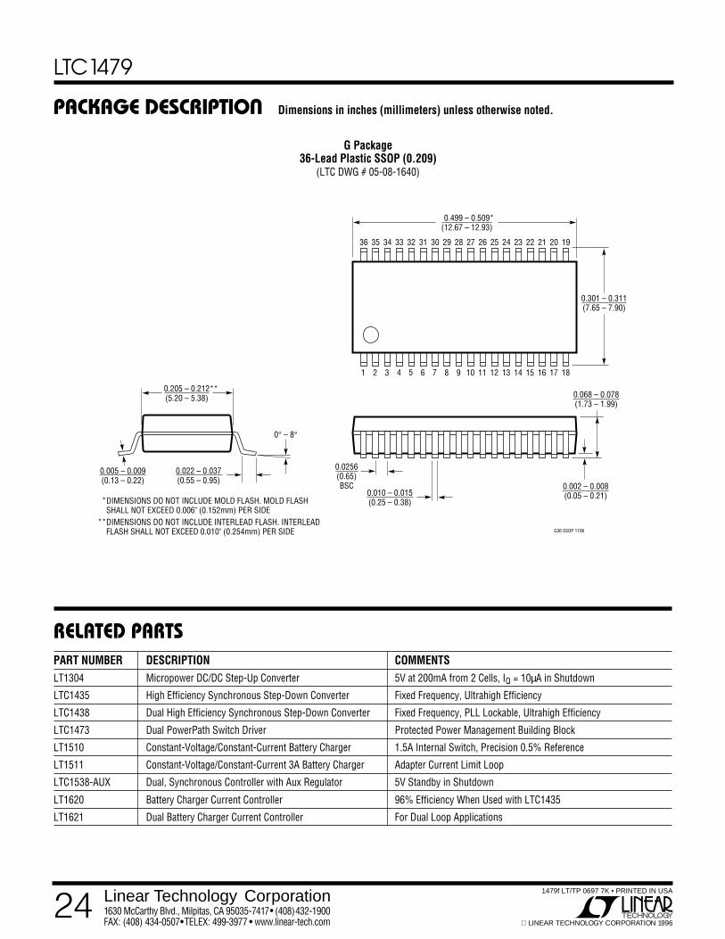
Dimensions in inches (millimeters) unless otherwise noted.PACKAGE DESCRIPTION
U
G Package36-Lead Plastic SSOP (0.209)
(LTC DWG # 05-08-1640)
RELATED PARTSPART NUMBER DESCRIPTION COMMENTSLT1304 Micropower DC/DC Step-Up Converter 5V at 200mA from 2 Cells, IQ = 10µA in Shutdown
LTC1435 High Efficiency Synchronous Step-Down Converter Fixed Frequency, Ultrahigh Efficiency
LTC1438 Dual High Efficiency Synchronous Step-Down Converter Fixed Frequency, PLL Lockable, Ultrahigh Efficiency
LTC1473 Dual PowerPath Switch Driver Protected Power Management Building Block
LT1510 Constant-Voltage/Constant-Current Battery Charger 1.5A Internal Switch, Precision 0.5% Reference
LT1511 Constant-Voltage/Constant-Current 3A Battery Charger Adapter Current Limit Loop
LTC1538-AUX Dual, Synchronous Controller with Aux Regulator 5V Standby in Shutdown
LT1620 Battery Charger Current Controller 96% Efficiency When Used with LTC1435
LT1621 Dual Battery Charger Current Controller For Dual Loop Applications
G36 SSOP 1196
0.005 – 0.009 (0.13 – 0.22)
0° – 8°
0.022 – 0.037 (0.55 – 0.95)
0.205 – 0.212** (5.20 – 5.38)
0.301 – 0.311 (7.65 – 7.90)
1 2 3 4 5 6 7 8 9 10 11 12 14 15 16 17 1813
0.499 – 0.509* (12.67 – 12.93)
2526 22 21 20 19232427282930313233343536
0.068 – 0.078 (1.73 – 1.99)
0.002 – 0.008 (0.05 – 0.21)
0.0256 (0.65) BSC
0.010 – 0.015 (0.25 – 0.38)DIMENSIONS DO NOT INCLUDE MOLD FLASH. MOLD FLASH
SHALL NOT EXCEED 0.006" (0.152mm) PER SIDE DIMENSIONS DO NOT INCLUDE INTERLEAD FLASH. INTERLEAD FLASH SHALL NOT EXCEED 0.010" (0.254mm) PER SIDE
*
**
Linear Technology Corporation1630 McCarthy Blvd., Milpitas, CA 95035-7417 (408) 432-1900FAX: (408) 434-0507 TELEX: 499-3977 www.linear-tech.com