Embed Size (px)
Citation preview
LTC3336
1Rev. 0
For more information www.analog.comDocument Feedback
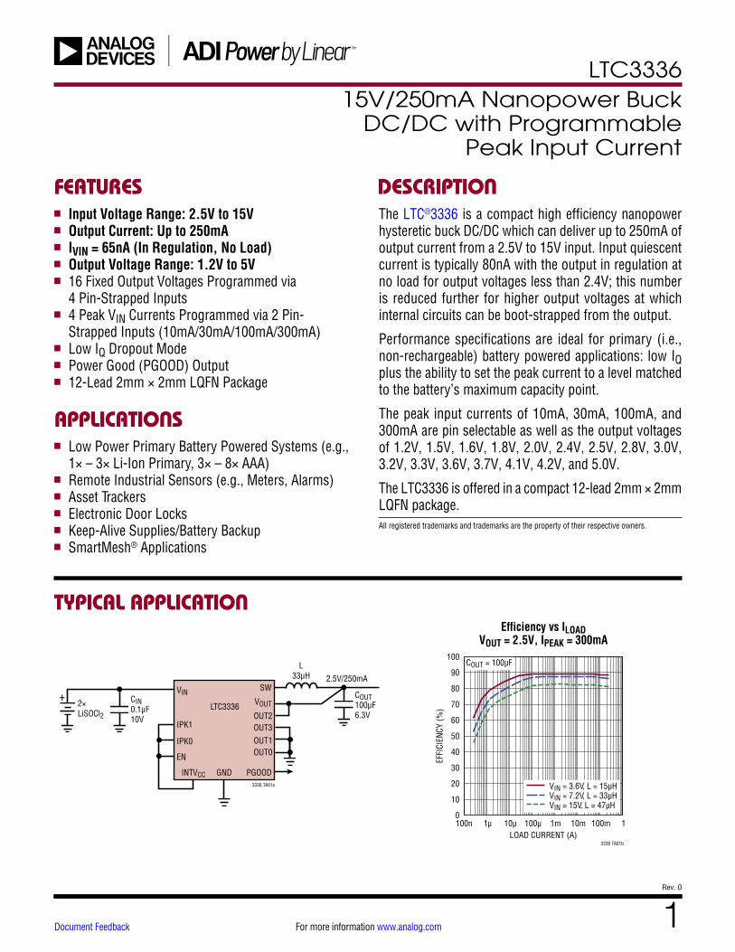
TYPICAL APPLICATION
FEATURES DESCRIPTION
15V/250mA Nanopower Buck DC/DC with Programmable
Peak Input Current
The LTC®3336 is a compact high efficiency nanopower hysteretic buck DC/DC which can deliver up to 250mA of output current from a 2.5V to 15V input. Input quiescent current is typically 80nA with the output in regulation at no load for output voltages less than 2.4V; this number is reduced further for higher output voltages at which internal circuits can be boot-strapped from the output.
Performance specifications are ideal for primary (i.e., non-rechargeable) battery powered applications: low IQ plus the ability to set the peak current to a level matched to the battery’s maximum capacity point.
The peak input currents of 10mA, 30mA, 100mA, and 300mA are pin selectable as well as the output voltages of 1.2V, 1.5V, 1.6V, 1.8V, 2.0V, 2.4V, 2.5V, 2.8V, 3.0V, 3.2V, 3.3V, 3.6V, 3.7V, 4.1V, 4.2V, and 5.0V.
The LTC3336 is offered in a compact 12-lead 2mm × 2mm LQFN package.
Efficiency vs ILOAD VOUT = 2.5V, IPEAK = 300mA
APPLICATIONS
n Input Voltage Range: 2.5V to 15V n Output Current: Up to 250mA n IVIN = 65nA (In Regulation, No Load) n Output Voltage Range: 1.2V to 5V n 16 Fixed Output Voltages Programmed via
4 Pin-Strapped Inputs n 4 Peak VIN Currents Programmed via 2 Pin-
Strapped Inputs (10mA/30mA/100mA/300mA) n Low IQ Dropout Mode n Power Good (PGOOD) Output n 12-Lead 2mm × 2mm LQFN Package
n Low Power Primary Battery Powered Systems (e.g., 1× – 3× Li-Ion Primary, 3× – 8× AAA)
n Remote Industrial Sensors (e.g., Meters, Alarms) n Asset Trackers n Electronic Door Locks n Keep-Alive Supplies/Battery Backup n SmartMesh® Applications
All registered trademarks and trademarks are the property of their respective owners.
3336 TA01a
+LTC3336
VIN
IPK1
IPK0
EN
SW
VOUT
PGOODINTVCC GND
L33μH 2.5V/250mA
COUT100μF6.3V
2×LiSOCl2
CIN0.1μF10V OUT2
OUT3OUT1OUT0
COUT = 100µF
VIN = 3.6V, L = 15µHVIN = 7.2V, L = 33µHVIN = 15V, L = 47µH
LOAD CURRENT (A)100n 1µ 10µ 100µ 1m 10m 100m 10
10
20
30
40
50
60
70
80
90
100
EFFI
CIEN
CY (%
)
3336 TA01b
LTC3336
2Rev. 0
For more information www.analog.com
ABSOLUTE MAXIMUM RATINGS
VIN Voltage ............................................. –0.3V to 16.5VEN, IPK[1:0], OUT[3:0] Voltage .................... –0.3V to 6VPGOOD Voltage ...........................–0.3V to (VOUT + 0.3V)PGOOD Current ...................................................... ±1mASW Current ......................................................... 400mAOperating Junction Temperature
Range (Notes 2, 3) ............................. –40°C to 125°CStorage Temperature Range .................. –65°C to 150°CReflow Peak Body Temperature (30sec Max)........ 260°C
(Note 1)
ORDER INFORMATION
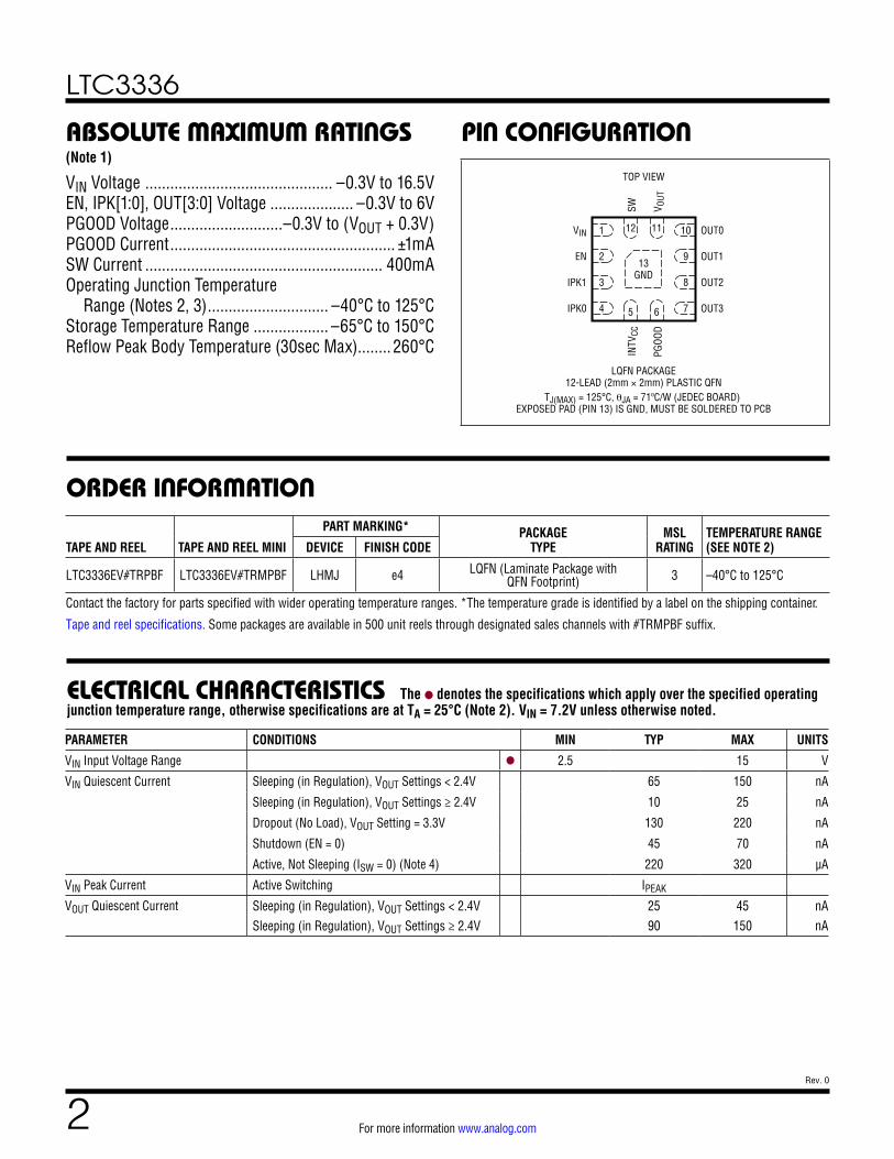
PIN CONFIGURATION
PARAMETER CONDITIONS MIN TYP MAX UNITS
VIN Input Voltage Range l 2.5 15 V
VIN Quiescent Current Sleeping (in Regulation), VOUT Settings < 2.4V 65 150 nA
Sleeping (in Regulation), VOUT Settings ≥ 2.4V 10 25 nA
Dropout (No Load), VOUT Setting = 3.3V 130 220 nA
Shutdown (EN = 0) 45 70 nA
Active, Not Sleeping (ISW = 0) (Note 4) 220 320 µA
VIN Peak Current Active Switching IPEAK
VOUT Quiescent Current Sleeping (in Regulation), VOUT Settings < 2.4VSleeping (in Regulation), VOUT Settings ≥ 2.4V
2590
45150
nAnA
TAPE AND REEL TAPE AND REEL MINI
PART MARKING* PACKAGE TYPE
MSL RATING
TEMPERATURE RANGE (SEE NOTE 2)DEVICE FINISH CODE
LTC3336EV#TRPBF LTC3336EV#TRMPBF LHMJ e4 LQFN (Laminate Package with QFN Footprint) 3 –40°C to 125°C
Contact the factory for parts specified with wider operating temperature ranges. *The temperature grade is identified by a label on the shipping container.
Tape and reel specifications. Some packages are available in 500 unit reels through designated sales channels with #TRMPBF suffix.
ELECTRICAL CHARACTERISTICS The l denotes the specifications which apply over the specified operating junction temperature range, otherwise specifications are at TA = 25°C (Note 2). VIN = 7.2V unless otherwise noted.
TOP VIEW
VIN
EN
IPK1
IPK0
OUT0
OUT1
OUT2
OUT3
SW V OUT
INTV
CC
PGOO
D
10
9
8
7
1
2
3
4
LQFN PACKAGE12-LEAD (2mm × 2mm) PLASTIC QFN
TJ(MAX) = 125°C, θJA = 71ºC/W (JEDEC BOARD) EXPOSED PAD (PIN 13) IS GND, MUST BE SOLDERED TO PCB
13GND
12 11
5 6
LTC3336
3Rev. 0
For more information www.analog.com
ELECTRICAL CHARACTERISTICS The l denotes the specifications which apply over the specified operating junction temperature range, otherwise specifications are at TA = 25°C (Note 2). VIN = 7.2V unless otherwise noted.
PARAMETER CONDITIONS MIN TYP MAX UNITS
Regulated Output Voltage (VOUT) 1.2V Output Setting: Sleep Threshold Wake-Up Threshold
l
l
1.164
1.204 1.196
1.236 V V
1.5V Output Setting: Sleep Threshold Wake-Up Threshold
l
l
1.455
1.505 1.495
1.545 V V
1.6V Output Setting: Sleep Threshold Wake-Up Threshold
l
l
1.552
1.605 1.595
1.648 V V
1.8V Output Setting: Sleep Threshold Wake-Up Threshold
l
l
1.746
1.806 1.794
1.854 V V
2.0V Output Setting: Sleep Threshold Wake-Up Threshold
l
l
1.940
2.007 1.993
2.060 V V
2.4V Output Setting: Sleep Threshold Wake-Up Threshold
l
l
2.328
2.408 2.392
2.472 V V
2.5V Output Setting: Sleep Threshold Wake-Up Threshold
l
l
2.425
2.508 2.492
2.575 V V
2.8V Output Setting: Sleep Threshold Wake-Up Threshold
l
l
2.716
2.809 2.791
2.884 V V
3.0V Output Setting: Sleep Threshold Wake-Up Threshold
l
l
2.910
3.010 2.990
3.090 V V
3.2V Output Setting: Sleep Threshold Wake-Up Threshold
l
l
3.104
3.211 3.189
3.296 V V
3.3V Output Setting: Sleep Threshold Wake-Up Threshold
l
l
3.201
3.311 3.289
3.399 V V
3.6V Output Setting: Sleep Threshold Wake-Up Threshold
l
l
3.492
3.612 3.588
3.708 V V
3.7V Output Setting: Sleep Threshold Wake-Up Threshold
l
l
3.589
3.712 3.688
3.811 V V
4.1V Output Setting: Sleep Threshold Wake-Up Threshold
l
l
3.977
4.114 4.086
4.223 V V
4.2V Output Setting: Sleep Threshold Wake-Up Threshold
l
l
4.074
4.214 4.186
4.326 V V
5.0V Output Setting: Sleep Threshold Wake-Up Threshold
l
l
4.850
5.017 4.983
5.150 V V
Power Good Threshold as Percentage of Output Setting
VOUT Falling (Note 5) l 90 92.5 95 %
PGOOD Output Low Voltage 10μA Into Pin l 0.2 V
PGOOD Output High Voltage 10μA Out of Pin l VOUT – 0.2 V
VOUT Pull-Down Resistor in Shutdown
EN = 0V 10 kΩ
VOUT Pull-Down Resistor in VOUT Overvoltage Condition
1 MΩ
VOUT Overvoltage Detection Threshold as Percentage of Output Setting
5 %
LTC3336
4Rev. 0
For more information www.analog.com
PARAMETER CONDITIONS MIN TYP MAX UNITS
IPEAK (Inductor Peak Current) 10mA IPEAK Setting, ISW Rising 8.7 10 13 mA
30mA IPEAK Setting, ISW Rising 26 30 39 mA
100mA IPEAK Setting, ISW Rising 87 100 130 mA
300mA IPEAK Setting, ISW Rising 260 300 390 mA
IVALLEY (Inductor Valley Current) 10mA IPEAK Setting, ISW Falling 9 mA
30mA IPEAK Setting, ISW Falling 27 mA
100mA IPEAK Setting, ISW Falling 90 mA
300mA IPEAK Setting, ISW Falling 270 mA
Deliverable Output Current 10mA IPEAK Setting l 8.3 mA
30mA IPEAK Setting l 25 mA
100mA IPEAK Setting l 83 mA
300mA IPEAK Setting l 250 mA
IZERO Inductor Current Going into Sleep, as a Percentage of IPEAK
17 %
P-Channel MOSFET Switch On-Resistance
10mA IPEAK Setting 16 Ω
30mA IPEAK Setting 5.3 Ω
100mA IPEAK Setting 1.6 Ω
300mA IPEAK Setting 0.53 Ω
N-Channel MOSFET Switch On-Resistance
10mA IPEAK Setting, 5V VOUT Setting 9.6 Ω
30mA IPEAK Setting, 5V VOUT Setting 3.2 Ω
100mA IPEAK Setting, 5V VOUT Setting 0.96 Ω
300mA IPEAK Setting, 5V VOUT Setting 0.32 Ω
P-Channel MOSFET Switch Leakage 0 15 nA
N-Channel MOSFET Switch Leakage 0 15 nA
INTVCC Voltage VOUT Settings < 2.4V, 0 ≤ I(INTVCC) ≤ 10µA 1.9 2 2.2 V
VOUT Settings ≥ 2.4V, 0 ≤ I(INTVCC) ≤ 10µA VOUT V
VUVLO Undervoltage Lockout VIN Rising 1.95 2.2 V
VIN Falling 1.5 1.75 V
VIH Digital Input High Voltage Pins IPK[1:0], OUT[3:0] INTVCC – 0.15V V
VIL Digital Input Low Voltage Pins IPK[1:0], OUT[3:0] 0.15 V
ELECTRICAL CHARACTERISTICS The l denotes the specifications which apply over the specified operating junction temperature range, otherwise specifications are at TA = 25°C (Note 2). VIN = 7.2V unless otherwise noted.
Note 1: Stresses beyond those listed under Absolute Maximum Ratings may cause permanent damage to the device. Exposure to any Absolute Maximum Rating condition for extended periods may affect device reliability and lifetime.Note 2: The LTC3336 is tested under pulsed load conditions such that TJ ≈ TA. The specifications over the –40°C to125°C operating junction temperature range are assured by design, characterization, and correlation with statistical process controls. Note that the maximum ambient temperature consistent with these specifications is determined by specific operating conditions in conjunction with board layout, the rated package thermal impedance, and other environmental factors.
Note 3: TJ is calculated from the ambient TA and power dissipation PD according to the following formula: TJ = TA + (PD • θJA).Note 4: Dynamic supply current is higher due to gate charge being delivered at the switching frequency.Note 5: The falling threshold is specified as a percentage of the average of the measured sleep and wake-up thresholds for each selected output voltage and the rising threshold is equal to the sleep threshold.
LTC3336
5Rev. 0
For more information www.analog.com
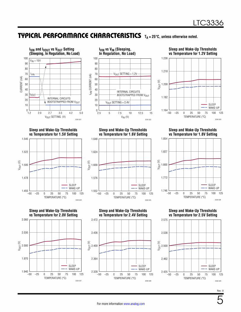
TYPICAL PERFORMANCE CHARACTERISTICS TA = 25°C, unless otherwise noted.
IVIN and IVOUT vs VOUT Setting (Sleeping, In Regulation, No Load)
IVIN vs VIN (Sleeping, In Regulation, No Load)
Sleep and Wake-Up Thresholds vs Temperature for 1.2V Setting
Sleep and Wake-Up Thresholds vs Temperature for 1.5V Setting
Sleep and Wake-Up Thresholds vs Temperature for 1.6V Setting
Sleep and Wake-Up Thresholds vs Temperature for 1.8V Setting
Sleep and Wake-Up Thresholds vs Temperature for 2.0V Setting
Sleep and Wake-Up Thresholds vs Temperature for 2.4V Setting
Sleep and Wake-Up Thresholds vs Temperature for 2.5V Setting
IVIN
IVOUT
VIN = 15V
VOUT SETTING (V)1.2 2.0 2.7 3.5 4.2 5.0
0
10
20
30
40
50
60
70
80
90
100
CURR
ENT
(nA)
3336 G01
INTERNAL CIRCUITS BOOTSTRAPPED FROM VOUT
VOUT SETTING = 1.2V
VOUT SETTING = 2.4V
VIN (V)2.5 5 7.5 10 12.5 15
0
10
20
30
40
50
60
70
80
90
100
I VIN
CUR
RENT
(nA)
3336 G02
INTERNAL CIRCUITS BOOTSTRAPPED FROM VOUT
TEMPERATURE (°C)–50 –25 0 25 50 75 100 125
1.164
1.182
1.200
1.218
1.236
V OUT
(V)
3336 G03
SLEEPWAKE-UP
TEMPERATURE (°C)–50 –25 0 25 50 75 100 125
1.455
1.478
1.500
1.522
1.545
V OUT
(V)
3336 G04
SLEEPWAKE-UP
TEMPERATURE (°C)–50 –25 0 25 50 75 100 125
1.552
1.576
1.600
1.624
1.648
V OUT
(V)
3336 G05
SLEEPWAKE-UP
TEMPERATURE (°C)–50 –25 0 25 50 75 100 125
1.746
1.773
1.800
1.827
1.854
V OUT
(V)
3336 G06
SLEEPWAKE-UP
TEMPERATURE (°C)–50 –25 0 25 50 75 100 125
1.940
1.970
2.000
2.030
2.060
V OUT
(V)
3336 G07
SLEEPWAKE-UP
TEMPERATURE (°C)–50 –25 0 25 50 75 100 125
2.328
2.364
2.400
2.436
2.472
V OUT
(V)
3336 G08
SLEEPWAKE-UP
TEMPERATURE (°C)–50 –25 0 25 50 75 100 125
2.425
2.462
2.500
2.538
2.575
V OUT
(V)
3336 G09
SLEEPWAKE-UP
LTC3336
6Rev. 0
For more information www.analog.com
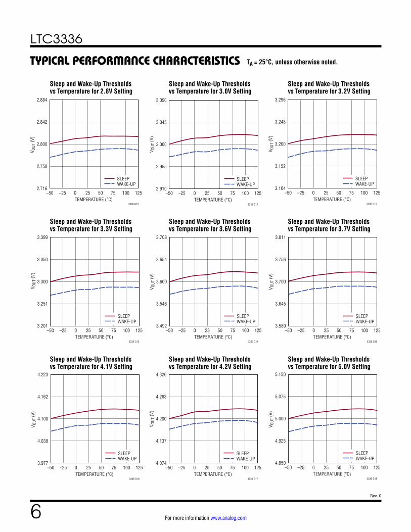
TYPICAL PERFORMANCE CHARACTERISTICS TA = 25°C, unless otherwise noted.
Sleep and Wake-Up Thresholds vs Temperature for 2.8V Setting
Sleep and Wake-Up Thresholds vs Temperature for 3.0V Setting
Sleep and Wake-Up Thresholds vs Temperature for 3.2V Setting
Sleep and Wake-Up Thresholds vs Temperature for 3.3V Setting
Sleep and Wake-Up Thresholds vs Temperature for 3.6V Setting
Sleep and Wake-Up Thresholds vs Temperature for 3.7V Setting
Sleep and Wake-Up Thresholds vs Temperature for 4.1V Setting
Sleep and Wake-Up Thresholds vs Temperature for 4.2V Setting
Sleep and Wake-Up Thresholds vs Temperature for 5.0V Setting
TEMPERATURE (°C)–50 –25 0 25 50 75 100 125
2.716
2.758
2.800
2.842
2.884
V OUT
(V)
3336 G10
SLEEPWAKE-UP
TEMPERATURE (°C)–50 –25 0 25 50 75 100 125
2.910
2.955
3.000
3.045
3.090
V OUT
(V)
3336 G11
SLEEPWAKE-UP
TEMPERATURE (°C)–50 –25 0 25 50 75 100 125
3.104
3.152
3.200
3.248
3.296
V OUT
(V)
3336 G12
SLEEPWAKE-UP
TEMPERATURE (°C)–50 –25 0 25 50 75 100 125
3.201
3.251
3.300
3.350
3.399
V OUT
(V)
3336 G13
SLEEPWAKE-UP
TEMPERATURE (°C)–50 –25 0 25 50 75 100 125
3.492
3.546
3.600
3.654
3.708
V OUT
(V)
3336 G14
SLEEPWAKE-UP
TEMPERATURE (°C)–50 –25 0 25 50 75 100 125
3.589
3.645
3.700
3.756
3.811
V OUT
(V)
3336 G15
SLEEPWAKE-UP
TEMPERATURE (°C)–50 –25 0 25 50 75 100 125
3.977
4.039
4.100
4.162
4.223
V OUT
(V)
3336 G16
SLEEPWAKE-UP
TEMPERATURE (°C)–50 –25 0 25 50 75 100 125
4.074
4.137
4.200
4.263
4.326
V OUT
(V)
3336 G17
SLEEPWAKE-UP
TEMPERATURE (°C)–50 –25 0 25 50 75 100 125
4.850
4.925
5.000
5.075
5.150
V OUT
(V)
3336 G18
SLEEPWAKE-UP
LTC3336
7Rev. 0
For more information www.analog.com
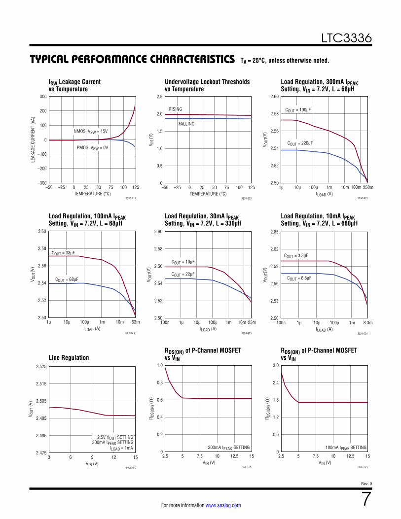
TYPICAL PERFORMANCE CHARACTERISTICS TA = 25°C, unless otherwise noted.
ISW Leakage Current vs Temperature
Undervoltage Lockout Thresholds vs Temperature
Load Regulation, 300mA IPEAK Setting, VIN = 7.2V, L = 68µH
Load Regulation, 100mA IPEAK Setting, VIN = 7.2V, L = 68µH
Load Regulation, 30mA IPEAK Setting, VIN = 7.2V, L = 330µH
Load Regulation, 10mA IPEAK Setting, VIN = 7.2V, L = 680µH
Line RegulationRDS(ON) of P-Channel MOSFET vs VIN
RDS(ON) of P-Channel MOSFET vs VIN
PMOS, VSW = 0V
NMOS, VSW = 15V
TEMPERATURE (°C)–50 –25 0 25 50 75 100 125
–300
–200
–100
0
100
200
300
LEAK
AGE
CURR
ENT
(nA)
3336 G19
RISING
FALLING
TEMPERATURE (°C)–50 –25 0 25 50 75 100 125
0
0.5
1.0
1.5
2.0
2.5
V IN
(V)
vs Temperature
3336 G20
COUT = 100μF
COUT = 220μF
100mILOAD (A)
1μ 10μ 100μ 1m 10m 250m2.50
2.52
2.54
2.56
2.58
2.60
V OUT
(V)
3336 G21
COUT = 33μF
COUT = 68μF
ILOAD (A)1μ 10μ 100μ 1m 10m 83m
2.50
2.52
2.54
2.56
2.58
2.60
V OUT
(V)
IN
3336 G22
COUT = 22μF
COUT = 10μF
10mILOAD (A)
100n 1μ 10μ 100μ 1m 25m2.50
2.52
2.54
2.56
2.58
2.60
V OUT
(V)
Setting, VIN = 7.2V, L = 330uH
3336 G23
COUT = 3.3μF
COUT = 6.8μF
ILOAD (A)100n 1μ 10μ 100μ 1m 8.3m
2.50
2.53
2.56
2.59
2.62
2.65
V OUT
(V)
Setting, VIN = 7.2V, L = 680uH
3336 G24
VIN (V)3 6 9 12 15
2.475
2.485
2.495
2.505
2.515
2.525
VOU
T (V
)
Line Regulation
3336 G25
2.5V VOUT SETTING
ILOAD = 1mA300mA IPEAK SETTING
300mA IPEAK SETTING
VIN (V)2.5 5 7.5 10 12.5 15
0
0.2
0.4
0.6
0.8
1.0
R DS(
ON) (
Ω)
DS(ON) IN
3336 G26
100mA IPEAK SETTING
VIN (V)2.5 5 7.5 10 12.5 15
0
0.6
1.2
1.8
2.4
3.0
R DS(
ON) (
Ω)
DS(ON) IN
3336 G27
LTC3336
8Rev. 0
For more information www.analog.com
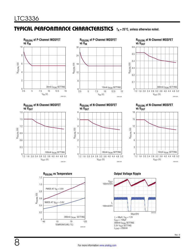
RDS(ON) of P-Channel MOSFET vs VIN
RDS(ON) of P-Channel MOSFET vs VIN
RDS(ON) of N-Channel MOSFET vs VOUT
RDS(ON) of N-Channel MOSFET vs VOUT
RDS(ON) of N-Channel MOSFET vs VOUT
RDS(ON) of N-Channel MOSFET vs VOUT
RDS(ON) vs Temperature Output Voltage Ripple
30mA IPEAK SETTING
VIN (V)2.5 5 7.5 10 12.5 15
0
2
4
6
8
10
R DS(
ON) (
Ω)
DS(ON) IN
3336 G28
10mA IPEAK SETTING
VIN (V)2.5 5 7.5 10 12.5 15
0
6
12
18
24
30
R DS(
ON) (
Ω)
DS(ON) IN
3336 G29
1.2 1.6 2.0 2.4 2.8 3.2 3.6 4.0 4.4 4.8 5.2
300mA IPEAK SETTING
VOUT (V)
0
0.1
0.2
0.3
0.4
0.5
0.6
R DS(
ON) (
Ω)
DS(ON) OUT
3336 G30
1.2 1.6 2.0 2.4 2.8 3.2 3.6 4.0 4.4 4.8 5.2
100mA IPEAK SETTING
VOUT (V)
0
0.3
0.6
0.9
1.2
1.5
1.8
R DS(
ON) (
Ω)
DS(ON) OUT
3336 G31
1.2 1.6 2.0 2.4 2.8 3.2 3.6 4.0 4.4 4.8 5.2
30mA IPEAK SETTING
VOUT (V)
0
1
2
3
4
5
6
R DS(
ON) (
Ω)
DS(ON) OUT
3336 G32
1.2 1.6 2.0 2.4 2.8 3.2 3.6 4.0 4.4 4.8 5.20
3
6
9
12
15
18
10mA IPEAK SETTING
VOUT (V)
R DS(
ON) (
Ω)
DS(ON) OUT
3336 G33
300mA IPEAK SETTING
PMOS AT VIN = 3.6V
NMOS AT VOUT = 3.6V
TEMPERATURE (°C)–40 15 70 125
0
0.2
0.4
0.6
0.8
1.0
1.2
R DS(
ON) (
Ω)
3336 G34
50µs/DIV
VOUT100mV/DIV
IL100mA/DIV
3336 G35
L = 68µH, VIN = 7.2VCOUT = 100µF300mA IPEAK SETTING
ILOAD = 250mA 2.5V VOUT SETTING
TYPICAL PERFORMANCE CHARACTERISTICS TA = 25°C, unless otherwise noted.

LTC3336
9Rev. 0
For more information www.analog.com
0A to 250mA Load Transient Power-Up TransientDynamic Output Voltage Change Between 1.5V and 1.8V
Efficiency vs ILOAD, VOUT = 1.2V, IPEAK = 300mA
Efficiency vs ILOAD, VOUT = 2.5V, IPEAK = 300mA
Efficiency vs ILOAD, VOUT = 5V, IPEAK = 300mA
Efficiency vs ILOAD, VOUT = 1.2V, IPEAK = 100mA
Efficiency vs ILOAD, VOUT = 2.5V, IPEAK = 100mA
Efficiency vs ILOAD, VOUT = 5V, IPEAK = 100mA
L = 68µH, VIN = 7.2V100ms/DIV
VOUT100mV/DIV
ILOAD100mA/DIV
3336 G36
COUT = 100µF300mA IPEAK SETTING2.5V VOUT SETTING
2ms/DIV
VOUT1V/DIV
VEN5V/DIV
3336 G37
L = 68µH, VIN = 7.2VCOUT = 100µF300mA IPEAK SETTING2.5V VOUT SETTINGILOAD = 250mA
1.8V (0010)1.5V (0011)
2ms/DIV
VOUT200mV/DIV
OUT01V/DIV
3336 G38
L = 68µH, VIN = 7.2VCOUT = 100µF300mA IPEAK SETTINGILOAD = 250mA
COUT = 100µF
VIN = 3.6V, L = 15µHVIN = 7.2V, L = 18µHVIN = 15V, L = 22µH
LOAD CURRENT (A)100n 1µ 10µ 100µ 1m 10m 100m 10
10
20
30
40
50
60
70
80
90
100
EFFI
CIEN
CY (%
)
VOUT = 1.2V, IPEAK = 300mA
3336 G39
COUT = 100µF
VIN = 3.6V, L = 15µHVIN = 7.2V, L = 33µHVIN = 15V, L = 47µH
LOAD CURRENT (A)100n 1µ 10µ 100µ 1m 10m 100m 10
10
20
30
40
50
60
70
80
90
100
EFFI
CIEN
CY (%
)
OUT PEAK
3336 G40
COUT = 100µF
VIN = 7.2V, L = 33µHVIN = 15V, L = 68µH
LOAD CURRENT (A)100n 1µ 10µ 100µ 1m 10m 100m 10
10
20
30
40
50
60
70
80
90
100
EFFI
CIEN
CY (%
)
VOUT = 5V, IPEAK = 300mA
3336 G41
COUT = 100µF
VIN = 3.6V, L = 47µHVIN = 7.2V, L = 68µHVIN = 15V, L = 68µH
LOAD CURRENT (A)100n 1µ 10µ 100µ 1m 10m 100m0
10
20
30
40
50
60
70
80
90
100
EFFI
CIEN
CY (%
)
OUT PEAK
3336 G42
COUT = 100µF
VIN = 3.6V, L = 47µHVIN = 7.2V, L = 100µHVIN = 15V, L = 120µH
LOAD CURRENT (A)100n 1µ 10µ 100µ 1m 10m 100m0
10
20
30
40
50
60
70
80
90
100
EFFI
CIEN
CY (%
)
OUT PEAK
3336 G43
COUT = 100µF
VIN = 7.2V, L = 100µHVIN = 15V, L = 180µH
LOAD CURRENT (A)100n 1µ 10µ 100µ 1m 10m 100m0
10
20
30
40
50
60
70
80
90
100
EFFI
CIEN
CY (%
)
OUT PEAK
3336 G44
TYPICAL PERFORMANCE CHARACTERISTICS TA = 25°C, unless otherwise noted.
LTC3336
10Rev. 0
For more information www.analog.com
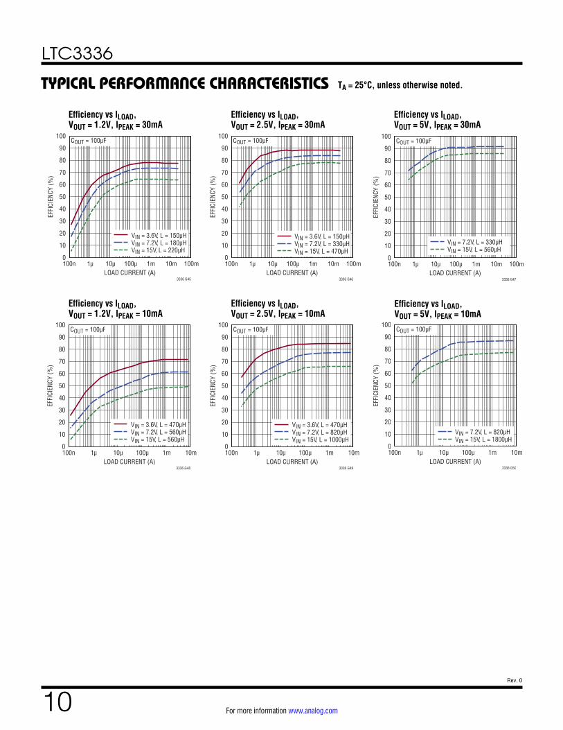
Efficiency vs ILOAD, VOUT = 1.2V, IPEAK = 30mA
Efficiency vs ILOAD, VOUT = 2.5V, IPEAK = 30mA
Efficiency vs ILOAD, VOUT = 5V, IPEAK = 30mA
Efficiency vs ILOAD, VOUT = 1.2V, IPEAK = 10mA
Efficiency vs ILOAD, VOUT = 2.5V, IPEAK = 10mA
Efficiency vs ILOAD, VOUT = 5V, IPEAK = 10mA
COUT = 100µF
VIN = 3.6V, L = 150µHVIN = 7.2V, L = 180µHVIN = 15V, L = 220µH
LOAD CURRENT (A)100n 1µ 10µ 100µ 1m 10m 100m0
10
20
30
40
50
60
70
80
90
100
EFFI
CIEN
CY (%
)
OUT PEAK
3336 G45
COUT = 100µF
VIN = 3.6V, L = 150µHVIN = 7.2V, L = 330µHVIN = 15V, L = 470µH
LOAD CURRENT (A)100n 1µ 10µ 100µ 1m 10m 100m0
10
20
30
40
50
60
70
80
90
100
EFFI
CIEN
CY (%
)
OUT PEAK
3336 G46
COUT = 100µF
VIN = 7.2V, L = 330µHVIN = 15V, L = 560µH
LOAD CURRENT (A)100n 1µ 10µ 100µ 1m 10m 100m0
10
20
30
40
50
60
70
80
90
100
EFFI
CIEN
CY (%
)
OUT PEAK
3336 G47
COUT = 100µF
VIN = 3.6V, L = 470µHVIN = 7.2V, L = 560µHVIN = 15V, L = 560µH
LOAD CURRENT (A)100n 1µ 10µ 100µ 1m 10m0
10
20
30
40
50
60
70
80
90
100
EFFI
CIEN
CY (%
)
OUT PEAK
3336 G48
COUT = 100µF
VIN = 3.6V, L = 470µHVIN = 7.2V, L = 820µHVIN = 15V, L = 1000µH
LOAD CURRENT (A)100n 1µ 10µ 100µ 1m 10m0
10
20
30
40
50
60
70
80
90
100
EFFI
CIEN
CY (%
)
OUT PEAK
3336 G49
COUT = 100µF
VIN = 7.2V, L = 820µHVIN = 15V, L = 1800µH
LOAD CURRENT (A)100n 1µ 10µ 100µ 1m 10m0
10
20
30
40
50
60
70
80
90
100
EFFI
CIEN
CY (%
)
VOUT = 5V, IPEAK = 10mA
3336 G50
TYPICAL PERFORMANCE CHARACTERISTICS TA = 25°C, unless otherwise noted.
LTC3336
11Rev. 0
For more information www.analog.com
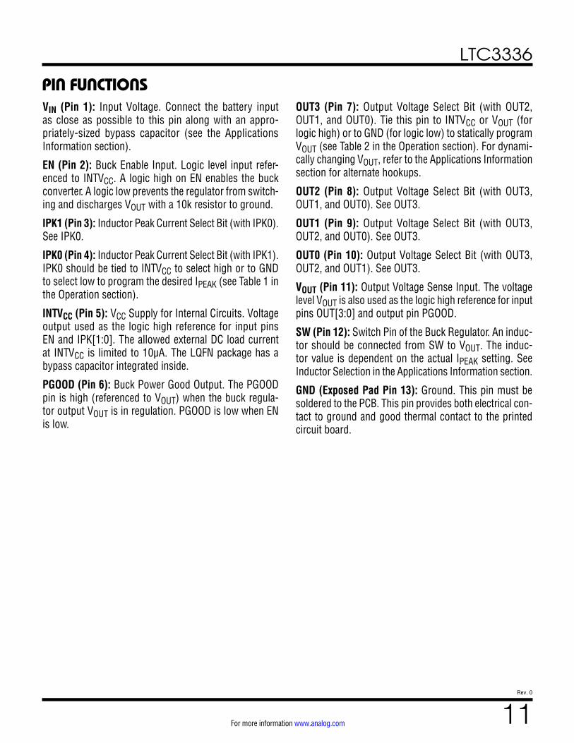
PIN FUNCTIONSVIN (Pin 1): Input Voltage. Connect the battery input as close as possible to this pin along with an appro-priately-sized bypass capacitor (see the Applications Information section).
EN (Pin 2): Buck Enable Input. Logic level input refer-enced to INTVCC. A logic high on EN enables the buck converter. A logic low prevents the regulator from switch-ing and discharges VOUT with a 10k resistor to ground.
IPK1 (Pin 3): Inductor Peak Current Select Bit (with IPK0). See IPK0.
IPK0 (Pin 4): Inductor Peak Current Select Bit (with IPK1). IPK0 should be tied to INTVCC to select high or to GND to select low to program the desired IPEAK (see Table 1 in the Operation section).
INTVCC (Pin 5): VCC Supply for Internal Circuits. Voltage output used as the logic high reference for input pins EN and IPK[1:0]. The allowed external DC load current at INTVCC is limited to 10µA. The LQFN package has a bypass capacitor integrated inside.
PGOOD (Pin 6): Buck Power Good Output. The PGOOD pin is high (referenced to VOUT) when the buck regula-tor output VOUT is in regulation. PGOOD is low when EN is low.
OUT3 (Pin 7): Output Voltage Select Bit (with OUT2, OUT1, and OUT0). Tie this pin to INTVCC or VOUT (for logic high) or to GND (for logic low) to statically program VOUT (see Table 2 in the Operation section). For dynami-cally changing VOUT, refer to the Applications Information section for alternate hookups.
OUT2 (Pin 8): Output Voltage Select Bit (with OUT3, OUT1, and OUT0). See OUT3.
OUT1 (Pin 9): Output Voltage Select Bit (with OUT3, OUT2, and OUT0). See OUT3.
OUT0 (Pin 10): Output Voltage Select Bit (with OUT3, OUT2, and OUT1). See OUT3.
VOUT (Pin 11): Output Voltage Sense Input. The voltage level VOUT is also used as the logic high reference for input pins OUT[3:0] and output pin PGOOD.
SW (Pin 12): Switch Pin of the Buck Regulator. An induc-tor should be connected from SW to VOUT. The induc-tor value is dependent on the actual IPEAK setting. See Inductor Selection in the Applications Information section.
GND (Exposed Pad Pin 13): Ground. This pin must be soldered to the PCB. This pin provides both electrical con-tact to ground and good thermal contact to the printed circuit board.
LTC3336
12Rev. 0
For more information www.analog.com
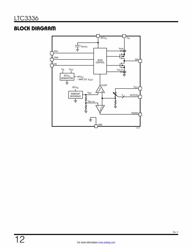
BLOCK DIAGRAMVIN
OUT[3:0]
EN
SW
VOUT
PGOOD
GND
IVALLEY
IPEAK
INTVCC
IPK0
IPK1
VREF_PG
VREF
BUCKCONTROL
3336 BD
CINTVCC
INTVCCGENERATION
INTVCC= MAX (2V, VOUT)
BANDGAPREFERENCE
4
+–
SLEEP
+–
INTVCC
VIN VOUT
LTC3336
13Rev. 0
For more information www.analog.com
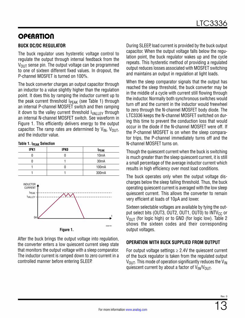
OPERATIONBUCK DC/DC REGULATOR
The buck regulator uses hysteretic voltage control to regulate the output through internal feedback from the VOUT sense pin. The output voltage can be programmed to one of sixteen different fixed values. In dropout, the P-channel MOSFET is turned on 100%.
The buck converter charges an output capacitor through an inductor to a value slightly higher than the regulation point. It does this by ramping the inductor current up to the peak current threshold IPEAK (see Table 1) through an internal P-channel MOSFET switch and then ramping it down to the valley current threshold IVALLEY through an internal N-channel MOSFET switch. See waveform in Figure 1. This efficiently delivers energy to the output capacitor. The ramp rates are determined by VIN, VOUT, and the inductor value.
Table 1. IPEAK SelectionIPK1 IPK0 IPEAK
0 0 10mA
0 1 30mA
1 0 100mA
1 1 300mA
Figure 1.
IPEAKIVALLEY
INDUCTORCURRENT
t0A
3336 F01
After the buck brings the output voltage into regulation, the converter enters a low quiescent current sleep state that monitors the output voltage with a sleep comparator. The inductor current is ramped down to zero current in a controlled manner before entering SLEEP.
During SLEEP, load current is provided by the buck output capacitor. When the output voltage falls below the regu-lation point, the buck regulator wakes up and the cycle repeats. This hysteretic method of providing a regulated output reduces losses associated with MOSFET switching and maintains an output in regulation at light loads.
When the sleep comparator signals that the output has reached the sleep threshold, the buck converter may be in the middle of a cycle with current still flowing through the inductor. Normally both synchronous switches would turn off and the current in the inductor would freewheel to zero through the N-channel MOSFET body diode. The LTC3336 keeps the N-channel MOSFET switched on dur-ing this time to prevent the conduction loss that would occur in the diode if the N-channel MOSFET were off. If the P-channel MOSFET is on when the sleep compara-tor trips, the P-channel immediately turns off and the N-channel MOSFET turns on.
Though the quiescent current when the buck is switching is much greater than the sleep quiescent current, it is still a small percentage of the average inductor current which results in high efficiency over most load conditions.
The buck operates only when the output voltage dis-charges below the sleep falling threshold. Thus, the buck operating quiescent current is averaged with the low sleep quiescent current. This allows the converter to remain very efficient at loads of 10μA and lower.
Sixteen selectable voltages are available by tying the out-put select bits (OUT3, OUT2, OUT1, OUT0) to INTVCC or VOUT (for logic high) or to GND (for logic low). Table 2 shows the sixteen codes and their corresponding output voltages.
OPERATION WITH BUCK SUPPLIED FROM OUTPUT
For output voltage settings ≥ 2.4V the quiescent current of the buck regulator is taken from the regulated output VOUT. This mode of operation significantly reduces the VIN quiescent current by about a factor of VIN/VOUT.
LTC3336
14Rev. 0
For more information www.analog.com
OPERATIONBUCK REGULATOR DROPOUT OPERATION
When the input supply voltage decreases towards the out-put voltage, the rate of change of inductor current during the upslope decreases, reducing the switching frequency of the current bursts. Further reduction in input supply voltage will eventually cause the P-channel MOSFET to be turned on 100%, i.e., DC. The output voltage will then be determined by the input voltage minus the voltage drop across the P-channel MOSFET and the inductor. The LTC3336 senses this state and enters a very low quiescent current state.
BUCK REGULATOR OUTPUT OVERVOLTAGE CONDITION AND INTERNAL CLAMP
An internal 1MΩ resistor pulls down VOUT if VOUT is higher than 5% above its regulation voltage. This should never happen in normal operation.
BUCK REGULATOR OUTPUT DISCHARGE
If EN is low, the buck regulator output is discharged through an internal 10k resistor.
Table 2. Buck Regulator Output Voltage Selection via OUT[3:0] PinsVOUT (V) OUT3 OUT2 OUT1 OUT0
1.2 0 0 0 1
1.5 0 0 1 1
1.6 0 0 0 0
1.8 0 0 1 0
2.0 0 1 1 0
2.4 0 1 0 1
2.5 0 1 0 0
2.8 0 1 1 1
3.0 1 0 0 0
3.2 1 1 0 0
3.3 1 0 0 1
3.6 1 0 1 0
3.7 1 0 1 1
4.1 1 1 0 1
4.2 1 1 1 0
5.0 1 1 1 1
Note: Underlined voltage values of 1.2V, 1.8V, 2.5V, and 3V can be set as power-up defaults. These voltage values can be “pin-strapped” with a single pin tied high during start-up, while the other pins can be dynamically set after start-up.
APPLICATIONS INFORMATION
INPUT CAPACITOR SELECTION
The input VIN should be bypassed with at least 0.1μF to GND. In cases where the input voltage is from a battery and the series resistance of the battery is high, a larger capacitor may be required to handle transients. A larger capacitor may also be necessary if the LTC3336 is sup-plied with an input voltage close to 2.5V (at higher IPEAK settings) to prevent the input voltage from transiently fall-ing below the undervoltage lockout threshold.
OUTPUT CAPACITOR SELECTION
The duration for which the regulator sleeps depends on the load current and the size of the output capacitor. The sleep time decreases as the load current increases and/or as the output capacitor decreases. The DC sleep hysteresis
window, Sleep Threshold – Wake-Up Threshold, is ±0.3% around the programmed output voltage. Ideally this means that the sleep time is determined by Equation 1.
tSLEEP = COUT • VOUT • 2 •
0.3%ILOAD
⎛⎝⎜
⎞⎠⎟
(1)
As the output capacitor decreases to much lower val-ues than described in Table 3, delays in the internal sleep comparator along with the load current may result in the VOUT voltage slewing past the ±0.3% thresholds. This will lengthen the sleep time and increase VOUT ripple.
If transient load currents above the IPEAK setting are required, then a larger capacitor can be used at the output. This capacitor will be continuously discharged
LTC3336
15Rev. 0
For more information www.analog.com
during this load condition. The capacitor can be sized using Equation 2 for an acceptable ripple VOUT
+ – VOUT–.
COUT = tLOAD •
ILOAD – 0.95 • IPEAK
VOUT+ – VOUT
–⎛
⎝⎜⎞
⎠⎟ (2)
In Equation 2, tLOAD is the duration of the excessive tran-sient load current, IPEAK is the programmed IPEAK setting and VOUT
+ – VOUT– is the desired VOUT ripple.
At zero or light load conditions VOUT should not exceed the typical 5% overvoltage threshold. Otherwise, it loses some power in the 1MΩ overvoltage pull-down resistor.
A standard surface mount ceramic capacitor can be used for COUT. These capacitors can be obtained from manu-facturers such as Vishay, Murata, TDK, and Taiyo Yuden.
Table 3. Minimum Required Buck Output Capacitor Size for a Sleep Time of 50µs at Max Load
VOUT (V)
IPEAK (mA)
COUT (µF)
1.2 10 6.8
1.2 30 22
1.2 100 68
1.2 300 220
2.5 10 3.3
2.5 30 10
2.5 100 33
2.5 300 100
5.0 10 2.2
5.0 30 4.7
5.0 100 22
5.0 300 47
INDUCTOR SELECTION
The buck is optimized to work with inductor values calcu-lated with Equation 3 or larger. The calculated values rep-resent a suitable trade-off between size and efficiency for typical applications. A larger inductor will benefit higher input voltage applications by reducing the switching fre-quency of the P-channel MOSFET switch, thereby improv-ing efficiency by reducing gate charge loss. Choose an inductor with a saturation current rating, ISAT, greater than the programmed IPEAK setting. The DC Resistance
(DCR) of the inductor can have an impact on efficiency as it is a source of loss. Trade-offs between price, size, and DCR should be evaluated. Equation 3 can be used to calculate the minimum inductor value that works well with the LTC3336 depending on VIN, VOUT, IPEAK and maxi-mum switching frequency ƒ. A good target for switching frequency is 2MHz.
Examples of inductor series to choose from: LPS4018 (0.56μH to 1000μH), MSS7348 (3.3μH to 1000μH), and MSS1210 (10μH to 10,000μH).
L = 1
ƒ • 10% •IPEAK •1
VIN − VOUT+ 1
VOUT
⎛⎝⎜
⎞⎠⎟
(3)
Explanation of symbols used in Equation 3 and how they are derived:
T = L •∆IVL
T = 1ƒ
∆I = IPEAK − IVALLEY = 10% •IPEAK
VL = Voltage Across Inductor
ƒ = Switching FrequencyT = TON + TOFF
TON = L •∆I
VIN − VOUT duration of
P-Channel MOSFET On
TOFF = L •∆I
VOUT duration of
P-Channel MOSFET Off
DYNAMIC OUTPUT VOLTAGE CHANGE
The selection bits OUT[3:0] can be driven from the out-puts of a microcontroller and dynamically changed while the buck is running.
A start-up default voltage, VDEFAULT, can be set with one (or more) pins tied high. Refer to Table 4 and the
APPLICATIONS INFORMATION
application: Microcontroller Supply with Dynamic Output Voltage Change in the Typical Applications section.
Table 4. Dynamic Operation Output Voltages with Single Pin Tied High
PIN TIED HIGH (DEFAULT)
VDEFAULT (V)
DYNAMIC OUTPUT VOLTAGES AVAILABLE WITH SINGLE PIN TIED HIGH
(V)
OUT0 1.2 1.2, 1.5, 2.4, 2.8, 3.3, 3.7, 4.1, 5.0
OUT1 1.8 1.5, 1.8, 2.0, 2.8, 3.6, 3.7, 4.2, 5.0
OUT2 2.5 2.0, 2.4, 2.5, 2.8, 3.2, 4.1, 4.2, 5.0
OUT3 3.0 3.0, 3.2, 3.3, 3.6, 3.7, 4.1, 4.2, 5.0
PCB LAYOUT CONSIDERATIONS
The LTC3336 switches large currents (relative to the IQ) at high frequencies. Special care should be given to the PCB layout to ensure stable, noise-free operation. Figure 2 depicts a recommended PCB layout to be utilized for the LTC3336, if a 2-layer PCB is being used. A few key guide-lines follow: All circulating high current paths should be kept as short as possible using wide traces. In particular, capacitor ground connections should connect by vias down to the ground plane in the shortest route possible. The bypass capacitors CIN and COUT should be placed as close to the IC as possible.
LTC3336
16Rev. 0
For more information www.analog.com
Figure 2. Recommended Component Placement on PCB
COUTCIN
10
9
8
7
1
2
3
4
12 11
5 6
L
LPS4018
LTC3336
TOP LAYER
BOTTOM COPPER LAYER (GROUND PLANE) CONNECTED TO GND
SEE TYPICAL APPLICATIONON FRONT PAGE
VIAS TO GROUND PLANE COMPONENT SIZES: CIN = 0201 COUT = 1210
3336 F02
VIN
EN
IPK1
IPK0
OUT0
OUT1
OUT2
OUT3
SW
V OUT
INTV
CC
PGOO
D
GND
APPLICATIONS INFORMATION
LTC3336
17Rev. 0
For more information www.analog.com
3336 TA03
+
LTC3336
VIN
OUT2IPK1IPK0
OUT3OUT1OUT0
EN
SWVOUT
PGOOD
INTVCC GND
L33μH 2.5V/250mA
COUT100μF6.3V
2×LiSOCl2
CIN0.1μF10V
7.2VIPEAK = 300mA
3336 TA04
+
LTC3336
VIN
OUT2
IPK1IPK0
OUT3OUT1OUT0
EN
SWVOUT
PGOOD
INTVCC GND
L330μH 2.5V/8mA
COUT3.3μF6.3V
LiSOCl2CIN0.1μF10V
3.6VIPEAK = 10mA
2.5V/250mA Buck Powered from 2× Lithium Thionyl Chloride Batteries
2.5V/8mA Buck Powered from Lithium Thionyl Chloride Battery
TYPICAL APPLICATIONS
LTC3336
18Rev. 0
For more information www.analog.com
3336 TA05
+
LTC3336
VIN
OUT0IPK1IPK0
OUT3OUT2OUT1
EN
SWVOUT
PGOOD
INTVCC GND
L15μH 1.2V/250mA
COUT220μF6.3V
LiSOCl2CIN0.1μF10V
3.6VIPEAK = 300mA
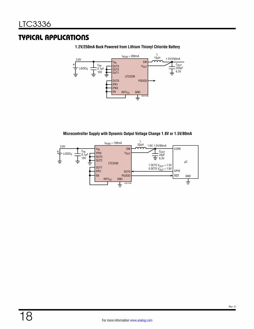
1.2V/250mA Buck Powered from Lithium Thionyl Chloride Battery
Microcontroller Supply with Dynamic Output Voltage Change 1.8V or 1.5V/80mA
TYPICAL APPLICATIONS
3336 TA06
+
LTC3336
VIN SW
OUT0
VOUT
PGOODINTVCC GND
GND
L33μH 1.8V, 1.5V/80mA
COUT33μF6.3V
LiSOCl2CIN0.1μF10V
3.6V
μC
CORE
GPIO
RST
1 SETS VOUT = 1.5V0 SETS VOUT = 1.8V
IPEAK = 100mA
OUT1IPK1
IPK0OUT3OUT2
EN
LTC3336
19Rev. 0
For more information www.analog.com
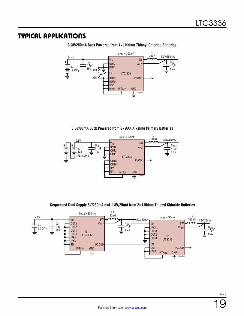
TYPICAL APPLICATIONS3.3V/250mA Buck Powered from 4× Lithium Thionyl Chloride Batteries
3336 TA07
+
LTC3336
VIN
EN
SWVOUT
PGOOD
INTVCC GND
L33μH 3.3V/250mA
COUT47μF6.3V
4×LiSOCl2
CIN0.1μF16V
14.4V
S1OFF
ON
IPEAK = 300mA
OUT2OUT1
OUT3OUT0IPK1IPK0
3336 TA08
+
LTC3336
VIN SWVOUT
PGOOD
INTVCC GND
L100μH 3.3V/80mA
COUT47μF6.3V
8×AAAALKALINE
CIN0.1μF16V
12.8V
+
IPEAK = 100mA
OUT3OUT0IPK1
IPK0OUT2OUT1
EN
3.3V/80mA Buck Powered from 8× AAA Alkaline Primary Batteries
Sequenced Dual Supply 5V/230mA and 1.8V/25mA from 2× Lithium Thionyl Chloride Batteries
U2LTC3336
VIN SWVOUT
PGOOD
INTVCC GND
L2330μH 1.8V/25mA
COUT210μF6.3V
3336 TA09
+
U1LTC3336
VIN SWVOUT
PGOODINTVCC GND
L122μH
5V/230mACOUT147μF6.3V
2×LiSOCl2
CIN0.1μF10V
7.2VIPEAK = 300mA
IPEAK = 30mA
IPK0
OUT0IPK1
OUT3OUT2OUT1
EN ENOUT1IPK0
IPK1OUT3
OUT0OUT2
LTC3336
20Rev. 0
For more information www.analog.com
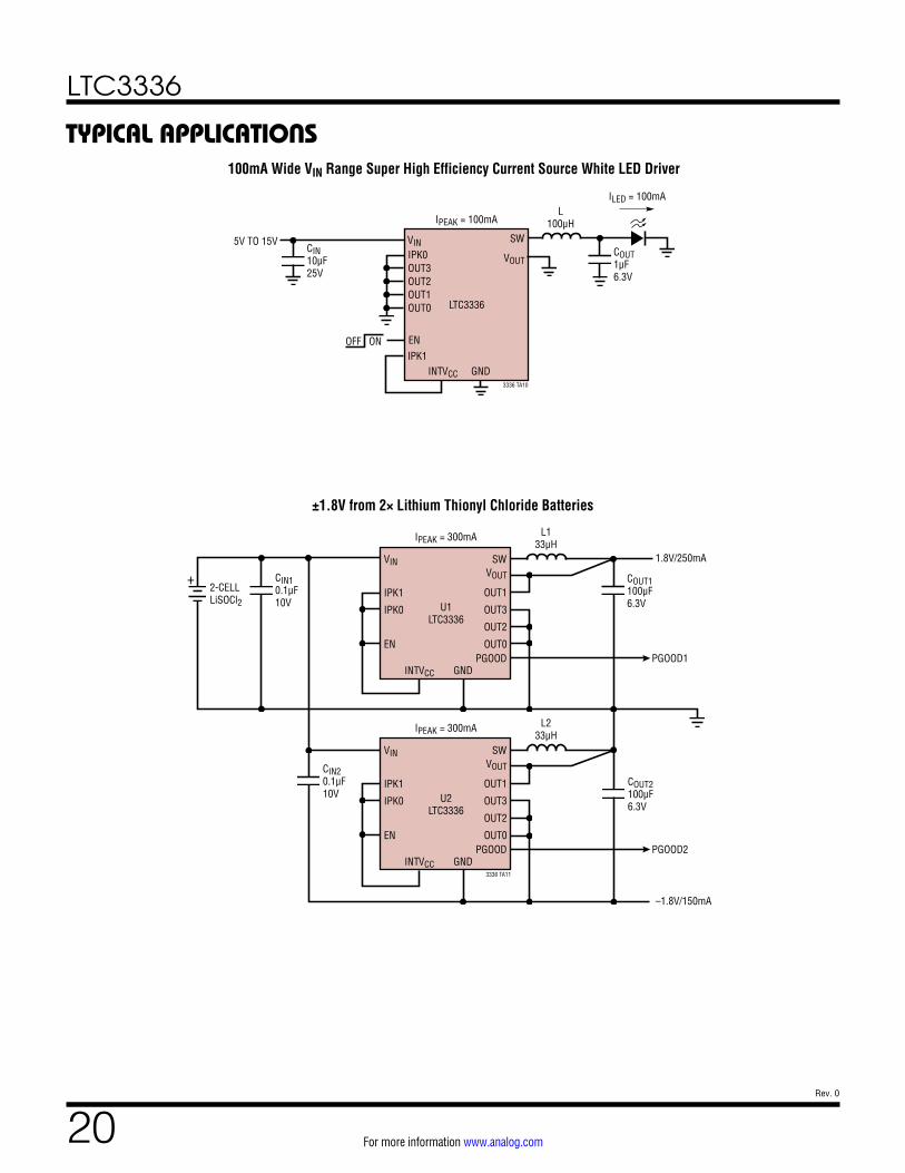
100mA Wide VIN Range Super High Efficiency Current Source White LED Driver
3336 TA10
LTC3336
VIN
EN
SW
INTVCC GND
L100μH
COUT1μF6.3V
CIN10μF25V
IPEAK = 100mA
5V TO 15V
OFF ONIPK1
IPK0OUT3
OUT1OUT0
OUT2
ILED = 100mA
VOUT
+
U1LTC3336
VIN SW
PGOOD PGOOD1
PGOOD2
INTVCC GND
L133μH
1.8V/250mA
COUT1100μF6.3V
2-CELLLiSOCl2
CIN10.1μF10V
IPEAK = 300mA
3336 TA11
L233μH
CIN20.1μF10V
IPK0
OUT0
IPK1 OUT1
OUT3
OUT2
EN
VOUT
U2LTC3336
VIN SW
PGOODINTVCC GND
IPEAK = 300mA
IPK0
OUT0
IPK1 OUT1
OUT3
OUT2
EN
VOUT
–1.8V/150mA
COUT2100μF6.3V
±1.8V from 2× Lithium Thionyl Chloride Batteries
TYPICAL APPLICATIONS
LTC3336
21Rev. 0
For more information www.analog.com
Information furnished by Analog Devices is believed to be accurate and reliable. However, no responsibility is assumed by Analog Devices for its use, nor for any infringements of patents or other rights of third parties that may result from its use. Specifications subject to change without notice. No license is granted by implication or otherwise under any patent or patent rights of Analog Devices.
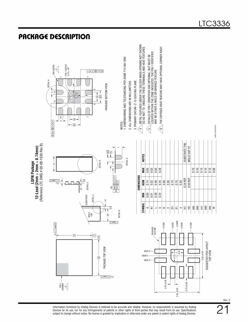
PACKAGE DESCRIPTIONLQ
FN P
acka
ge12
-Lea
d (2
mm
× 2
mm
× 0
.74m
m)
(Ref
eren
ce L
TC D
WG
# 05
-08-
1530
Rev
B)
DETA
IL B
A
PACK
AGE
TOP
VIEW
5PIN
1CO
RNER
Y
X
aaa
Z2×
12b
PACK
AGE
BOTT
OM V
IEW
4
6
SEE
NOTE
S
E
D
b
e
e
b
E1
D1
DETA
IL B
SUBS
TRAT
EM
OLD
CAP
// bbb Z
Z
H2H1
L
DETA
IL A
DETA
IL C
SUGG
ESTE
D PC
B LA
YOUT
TOP
VIEW0.0000
0.00
00
0.75
00
0.25
00
0.25
00
0.75
00
0.2500
0.2500
DETA
IL A
PIN
1 NO
TCH
0.14
× 4
5°
1112
65
1 4
10 7
aaa Z 2×
MX
YZ
ccc
MXY Z ccc
MX
YZ
eee
MZ
fff
PACK
AGE
OUTL
INE
0.25
±0.
05
0.70
±0.
05
2.50
±0.
05
2.50
±0.
05
LQFN
12
0618
REV
B
0.25
0
0.70
0.70
ddd Z12×
Z
A1 DETA
IL C
SYM
BOL
A A1 L b D E D1 E1 e H1 H2 aaa
bbb
ccc
ddd
eee
fff
MIN
0.65
0.01
0.30
0.22
NOM
0.74
0.02
0.40
0.25
2.00
2.00
0.70
0.70
0.50
0.24
REF
0.50
REF
MAX
0.83
0.03
0.50
0.28
0.10
0.10
0.10
0.10
0.15
0.08
NOTE
S
DIM
ENSI
ONS
NOTE
S:1.
DIM
ENSI
ONIN
G AN
D TO
LERA
NCIN
G PE
R AS
ME
Y14.
5M-1
994
2. A
LL D
IMEN
SION
S AR
E IN
MIL
LIM
ETER
S
3. P
RIM
ARY
DATU
M -Z
- IS
SEAT
ING
PLAN
E
MET
AL F
EATU
RES
UNDE
R TH
E SO
LDER
MAS
K OP
ENIN
G NO
T SH
OWN
SO
AS
NOT
TO O
BSCU
RE T
HESE
TER
MIN
ALS
AND
HEAT
FEA
TURE
S
54
DETA
ILS
OF P
IN 1
IDEN
TIFI
ER A
RE O
PTIO
NAL,
BUT
MUS
T BE
LO
CATE
D W
ITHI
N TH
E ZO
NE IN
DICA
TED.
THE
PIN
1 ID
ENTI
FIER
M
AY B
E EI
THER
A M
OLD
OR M
ARKE
D FE
ATUR
E
6TH
E EX
POSE
D HE
AT F
EATU
RE M
AY H
AVE
OPTI
ONAL
COR
NER
RADI
I
ee/2
SUBS
TRAT
E TH
KM
OLD
CAP
HT
LTC3336
22Rev. 0
For more information www.analog.com ANALOG DEVICES, INC. 2021
07/21www.analog.com
RELATED PARTS
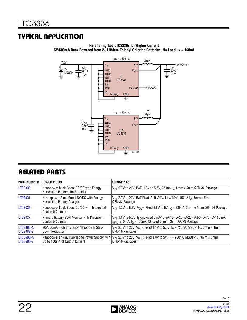
TYPICAL APPLICATION
PART NUMBER DESCRIPTION COMMENTS
LTC3330 Nanopower Buck-Boost DC/DC with Energy Harvesting Battery Life Extender
VIN: 2.7V to 20V, BAT: 1.8V to 5.5V, 750nA IQ, 5mm x 5mm QFN-32 Package
LTC3331 Nsanopower Buck-Boost DC/DC with Energy Harvesting Battery Charger
VIN: 2.7V to 20V, BAT Float: 3.45V/4V/4.1V/4.2V, 950nA IQ, 5mm × 5mm QFN-32 Package
LTC3335 Nanopower Buck-Boost DC/DC with Integrated Coulomb Counter
VIN: 1.8V to 5.5V, VOUT: Fixed 1.8V to 5V, IQ = 680nA, 3mm × 4mm QFN-20 Package
LTC3337 Primary Battery SOH Monitor with Precision Coulomb Counter
VIN: 1.8V to 5.5V, IPEAK: Fixed 5mA/10mA/15mA/20mA/25mA/50mA/75mA/100mA, IBAL: ±10mA, IQ = 100nA, 12-Lead 2mm × 2mm GQFN Package
LTC3388-1/ LTC3388-3
20V, 50mA High Efficiency Nanopower Step-Down Regulator
VIN: 2.7V to 20V, VOUT: Fixed 1.1V to 5.5V, IQ = 720nA, MSOP-10, 3mm × 3mm DFN-10 Packages
LTC3588-1/ LTC3588-2
Nanopower Energy Harvesting Power Supply with Up to 100mA of Output Current
VIN: 2.7V to 20V, VOUT: Fixed 1.8V to 5V, IQ = 950nA, MSOP-10, 3mm × 3mm DFN-10 Packages
+
U1LTC3336
VIN SW
PGOOD PGOOD
INTVCC GND
L122μH
5V/500mACOUT220μF6.3V
2×LiSOCl2
CIN10.1μF10V
7.2VIPEAK = 300mA
3336 TA02
U2LTC3336
VIN SW
VOUT
INTVCC GND
L222μH
IPEAK = 300mA
CIN20.1μF10V
IPK0
OUT0IPK1
OUT3OUT2OUT1
EN
IPK0
OUT0IPK1
OUT3OUT2OUT1
EN
VOUT
Paralleling Two LTC3336s for Higher Current 5V/500mA Buck Powered from 2× Lithium Thionyl Chloride Batteries, No Load IIN = 160nA