Embed Size (px)
Citation preview
M28 Hardware ManualRelease 1
ARIES Embedded GmbH
August 30, 2016

CONTENTS
1 About this manual 11.1 Imprint . . . . . . . . . . . . . . . . . . . . . . . . . . . . . . . . . . . . . . . . . . . . . . . . . . 11.2 Disclaimer . . . . . . . . . . . . . . . . . . . . . . . . . . . . . . . . . . . . . . . . . . . . . . . . 11.3 Copyright . . . . . . . . . . . . . . . . . . . . . . . . . . . . . . . . . . . . . . . . . . . . . . . . . 11.4 Registered Trademarks . . . . . . . . . . . . . . . . . . . . . . . . . . . . . . . . . . . . . . . . . . 11.5 Care and Maintenance . . . . . . . . . . . . . . . . . . . . . . . . . . . . . . . . . . . . . . . . . . 21.6 Change Log . . . . . . . . . . . . . . . . . . . . . . . . . . . . . . . . . . . . . . . . . . . . . . . 2
2 Overview 32.1 Feature Set . . . . . . . . . . . . . . . . . . . . . . . . . . . . . . . . . . . . . . . . . . . . . . . . 32.2 Block Diagram . . . . . . . . . . . . . . . . . . . . . . . . . . . . . . . . . . . . . . . . . . . . . . 42.3 Dimensions . . . . . . . . . . . . . . . . . . . . . . . . . . . . . . . . . . . . . . . . . . . . . . . . 52.4 MXM Connector . . . . . . . . . . . . . . . . . . . . . . . . . . . . . . . . . . . . . . . . . . . . . 52.5 Part Label . . . . . . . . . . . . . . . . . . . . . . . . . . . . . . . . . . . . . . . . . . . . . . . . . 62.6 Parts Overview . . . . . . . . . . . . . . . . . . . . . . . . . . . . . . . . . . . . . . . . . . . . . . 7
3 Resources 93.1 Pin Out . . . . . . . . . . . . . . . . . . . . . . . . . . . . . . . . . . . . . . . . . . . . . . . . . . 93.2 Interfaces . . . . . . . . . . . . . . . . . . . . . . . . . . . . . . . . . . . . . . . . . . . . . . . . . 133.3 UART . . . . . . . . . . . . . . . . . . . . . . . . . . . . . . . . . . . . . . . . . . . . . . . . . . . 173.4 USB . . . . . . . . . . . . . . . . . . . . . . . . . . . . . . . . . . . . . . . . . . . . . . . . . . . 183.5 Analogue . . . . . . . . . . . . . . . . . . . . . . . . . . . . . . . . . . . . . . . . . . . . . . . . . 183.6 Audio . . . . . . . . . . . . . . . . . . . . . . . . . . . . . . . . . . . . . . . . . . . . . . . . . . . 193.7 GPIO . . . . . . . . . . . . . . . . . . . . . . . . . . . . . . . . . . . . . . . . . . . . . . . . . . . 193.8 GPMI . . . . . . . . . . . . . . . . . . . . . . . . . . . . . . . . . . . . . . . . . . . . . . . . . . . 203.9 Keypad . . . . . . . . . . . . . . . . . . . . . . . . . . . . . . . . . . . . . . . . . . . . . . . . . . 203.10 PWM . . . . . . . . . . . . . . . . . . . . . . . . . . . . . . . . . . . . . . . . . . . . . . . . . . . 203.11 Rotary Decoder . . . . . . . . . . . . . . . . . . . . . . . . . . . . . . . . . . . . . . . . . . . . . . 213.12 Timer . . . . . . . . . . . . . . . . . . . . . . . . . . . . . . . . . . . . . . . . . . . . . . . . . . . 213.13 Power Supply . . . . . . . . . . . . . . . . . . . . . . . . . . . . . . . . . . . . . . . . . . . . . . . 213.14 Power Switch . . . . . . . . . . . . . . . . . . . . . . . . . . . . . . . . . . . . . . . . . . . . . . . 223.15 Reset . . . . . . . . . . . . . . . . . . . . . . . . . . . . . . . . . . . . . . . . . . . . . . . . . . . 223.16 Supply Modes . . . . . . . . . . . . . . . . . . . . . . . . . . . . . . . . . . . . . . . . . . . . . . 23
i

ii
CHAPTER
ONE
ABOUT THIS MANUAL
1.1 Imprint
Adress:
ARIES Embedded GmbH
Schöngeisinger Str. 84
D-82256 Fürstenfedbruck
Germany
Phone:
+49 (0) 8141/36 367-0
Fax:
+49 (0) 8141/36 367-67
1.2 Disclaimer
ARIES Embedded does not guarantee that the information in this document is up-to-date, correct, complete or of goodquality. Liability claims against ARIES Embedded, referring to material or non-material related damages caused,due to usage or non-usage of the information given in this document, or due to usage of erroneous or incompleteinformation, are exempted, as long as there is no proven intentional or negligent fault of ARIES Embedded. ARIESEmbedded explicitly reserves the rights to change or add to the contents of this Preliminary User’s Manual or parts ofit without notification.
1.3 Copyright
This document may not be copied, reproduced, translated, changed or distributed, completely or partially in any formwithout the written approval of ARIES Embedded GmbH.
1.4 Registered Trademarks
The contents of this document may be subject of intellectual property rights (including but not limited to copyright,trademark, or patent rights). Any such rights that are not expressly licensed or already owned by a third party arereserved by ARIES Embedded GmbH.
1
M28 Hardware Manual, Release 1
1.5 Care and Maintenance
• Keep the device dry. Precipitation, humidity, and all types of liquids or moisture can contain minerals that willcorrode electronic circuits. If your device does get wet, allow it to dry completely.
• Do not use or store the device in dusty, dirty areas. Its moving parts and electronic components can be damaged.
• Do not store the device in hot areas. High temperatures can shorten the life of electronic devices, damagebatteries, and warp or melt certain plastics.
• Do not store the device in cold areas. When the device returns to its normal temperature, moisture can forminside the device and damage electronic circuit boards.
• Do not attempt to open the device.
• Do not drop, knock, or shake the device. Rough handling can break internal circuit boards and fine mechanics.
• Do not use harsh chemicals, cleaning solvents, or strong detergents to clean the device.
• Do not paint the device. Paint can clog the moving parts and prevent proper operation.
• Unauthorized modifications or attachments could damage the device and may violate regulations governingradio devices.
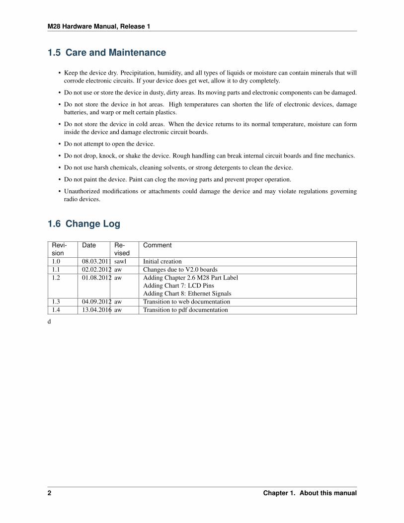
1.6 Change Log
Revi-sion
Date Re-vised
Comment
1.0 08.03.2011 sawl Initial creation1.1 02.02.2012 aw Changes due to V2.0 boards1.2 01.08.2012 aw Adding Chapter 2.6 M28 Part Label
Adding Chart 7: LCD PinsAdding Chart 8: Ethernet Signals
1.3 04.09.2012 aw Transition to web documentation1.4 13.04.2016 aw Transition to pdf documentation
d
2 Chapter 1. About this manual
CHAPTER
TWO
OVERVIEW
The M28 module is the fast, flexible and reliable System On Module (SOM) solution based on the new i.MX287processor by Freescale Semiconductor. The i.MX287 is the most feature rich device in the i.MX28 family. Optimizedfor performance and power consumption, the i.MX287 boasts of a premium feature set that includes: dual CAN, dualEthernet, and LCD touch screen. The i.MX287 is an ideal fit for portable devices that require rich user interfaces withhigh color displays for presented information and user interaction.
The M28 System On Module targets
• Human Machine Interface (HMI) panels: industrial, home.
• Industrial drive, PLC, I/O control display, factory robotics display.
• Graphical remote controls.
• Handheld scanners and printers.
• Electronic point-of-sale (POS) terminals.
• Smart energy gateways/meters.
• Media gateways.
• Portable medical devices.
• Media phones, VoIP.
• Automotive infotainment.
2.1 Feature Set
The M28 System on Module features
• i.MX287, up to 454MHz speed
• 128MB DDR2 DRAM, 256MB optionally available
• 256 MB NAND Flash
• 70 x 35mm size
• 230 Pins edge connector „MXM“
• Interfaces:
– LCD Controller 800x480 with Touchscreen support
– up to 2 x 10/100MBit Ethernet with IEEE1588 support
– up to 2 x CAN
3
M28 Hardware Manual, Release 1
– up to 2 x USB2.0 (1 x OTG/Device)
– up to 4 x UART
– 2 x I²C
– up to 4 x SPI
– up to 4 x SDIO
– I²S
• Security features:
– Read-only unique ID for Digital Rights Management (DRM) algorithms
– Secure boot using 128-bit AES hardware decryption
– SHA-1 and SHA256 hashing hardware
– High assurance boot (HAB4)
– Up to 8x8 keypad matrix with button-detect circuit
– Multiplexing on several functional blocks
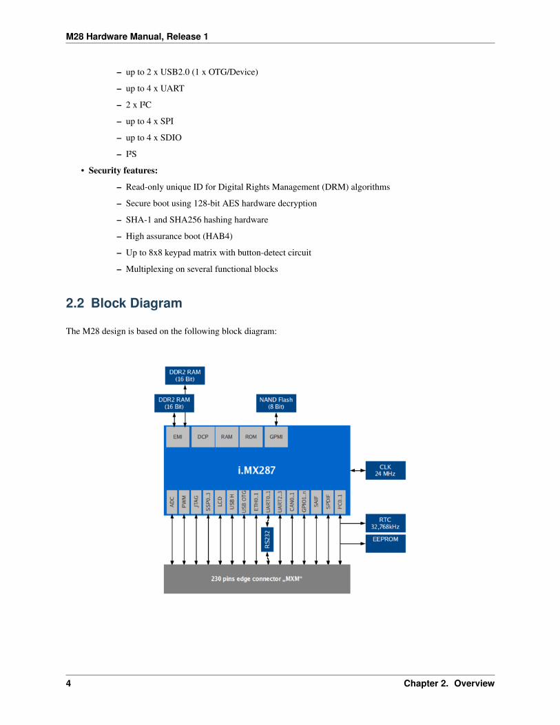
2.2 Block Diagram
The M28 design is based on the following block diagram:
4 Chapter 2. Overview
M28 Hardware Manual, Release 1
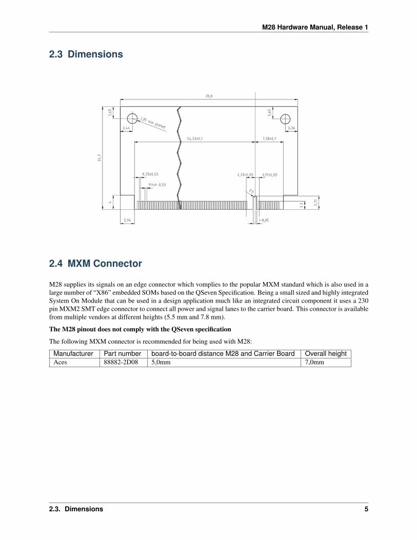
2.3 Dimensions
2.4 MXM Connector
M28 supplies its signals on an edge connector which vomplies to the popular MXM standard which is also used in alarge number of “X86” embedded SOMs based on the QSeven Specification. Being a small sized and highly integratedSystem On Module that can be used in a design application much like an integrated circuit component it uses a 230pin MXM2 SMT edge connector to connect all power and signal lanes to the carrier board. This connector is availablefrom multiple vendors at different heights (5.5 mm and 7.8 mm).
The M28 pinout does not comply with the QSeven specification
The following MXM connector is recommended for being used with M28:
Manufacturer Part number board-to-board distance M28 and Carrier Board Overall heightAces 88882-2D08 5,0mm 7,0mm
2.3. Dimensions 5
M28 Hardware Manual, Release 1
M28 provides
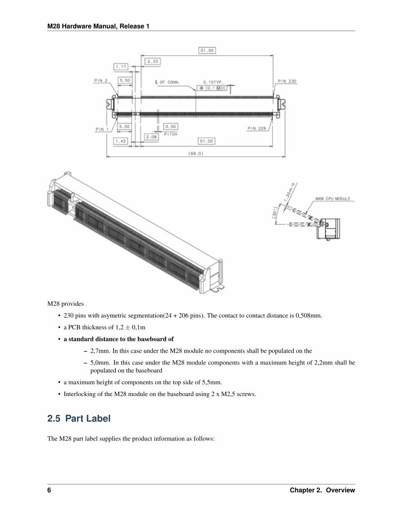
• 230 pins with asymetric segmentation(24 + 206 pins). The contact to contact distance is 0,508mm.
• a PCB thickness of 1,2 ± 0,1m
• a standard distance to the baseboard of
– 2,7mm. In this case under the M28 module no components shall be populated on the
– 5,0mm. In this case under the M28 module components with a maximum height of 2,2mm shall bepopulated on the baseboard
• a maximum height of components on the top side of 5,5mm.
• Interlocking of the M28 module on the baseboard using 2 x M2,5 screws.
2.5 Part Label
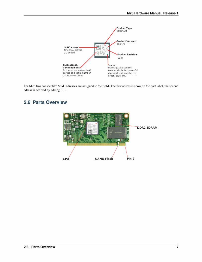
The M28 part label supplies the product information as follows:
6 Chapter 2. Overview
M28 Hardware Manual, Release 1
For M28 two consecutive MAC adresses are assigned to the SoM. The first adress is show on the part label, the secondadress is achived by adding “1”.
2.6 Parts Overview
2.6. Parts Overview 7

M28 Hardware Manual, Release 1
8 Chapter 2. Overview
CHAPTER
THREE
RESOURCES
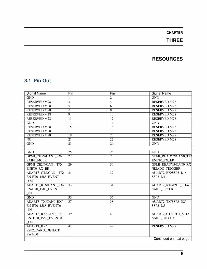
3.1 Pin Out
Signal Name Pin Pin Signal NameGND 1 2 GNDRESERVED M28 3 4 RESERVED M28RESERVED M28 5 6 RESERVED M28RESERVED M28 7 8 RESERVED M28RESERVED M28 9 10 RESERVED M28RESERVED M28 11 12 RESERVED M28GND 13 14 GNDRESERVED M28RESERVED M28
1517
1618
RESERVED M28RESERVED M28
RESERVED M28 19 20 RESERVED M28NC 21 22 RESERVED M28GND 23 24 GND
GND 25 26 GNDGPMI_CE3N/CAN1_RX/SAIF1_MCLK
27 28 GPMI_READY2/CAN0_TX/ENET0_TX_ER
GPMI_CE2N/CAN1_TX/ENET0_RX_ER
29 30 GPMI_READY3/CAN0_RX/HSADC_TRIGGER
AUART3_CTS/CAN1_TX/EN-ET0_1588_EVENT1_OUT
31 32 AUART2_RX/SSP3_D1/SSP3_D4
AUART3_RTS/CAN1_RX/EN-ET0_1588_EVENT1_IN
33 34 AUART2_RTS/I2C1_SDA/SAIF1_LRCLK
GND 35 36 GNDAUART3_TX/CAN0_RX/EN-ET0_1588_EVENT0_IN
37 38 AUART2_TX/SSP3_D2/SSP3_D5
AUART3_RX/CAN0_TX/EN- ET0_1588_EVENT0_OUT
39 40 AUART2_CTS/I2C1_SCL/SAIF1_BITCLK
AUART1_RX/SSP2_CARD_DETECT/PWM_0
41 42 RESERVED M28
Continued on next page
9
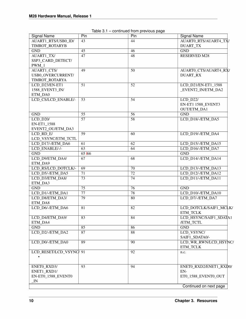
M28 Hardware Manual, Release 1
Table 3.1 – continued from previous pageSignal Name Pin Pin Signal NameAUART1_RTS/USB0_ID/TIMROT_ROTARYB
43 44 AUART0_RTS/AUART4_TX/DUART_TX
GND 45 46 GNDAUART1_TX/SSP3_CARD_DETECT/PWM_1
47 48 RESERVED M28
AUART1_CTS/USB0_OVERCURRENT/TIMROT_ROTARYA
49 50 AUART0_CTS/AUART4_RX/DUART_RX
LCD_D23/EN-ET11588_EVENT3_IN/ETM_DA0
51 52 LCD_D21/EN-ET1_1588_EVENT2_IN/ETM_DA2
LCD_CS/LCD_ENABLE/- 53 54 LCD_D22/EN-ET1 1588_EVENT3OUT/ETM_DA1
GND 55 56 GNDLCD_D20/EN-ET1_1588EVENT2_OU/ETM_DA3
57 58 LCD_D18/-/ETM_DA5
LCD_RD_E/LCD_VSYNC/ETM_TCTL
59 60 LCD_D19/-/ETM_DA4
LCD_D17/-/ETM_DA6 61 62 LCD_D15/-/ETM_DA15LCD_ENABLE/-/- 63 64 LCD_D16/-/ETM_DA7GND 65 |66 GNDLCD_D9/ETM_DA4/ETM_DA9
67 68 LCD_D14/-/ETM_DA14
LCD_RS/LCD_DOTCLK/- 69 70 LCD_D13/-/ETM_DA13LCD_D5/-/ETM_DA5 71 72 LCD_D12/-/ETM_DA12LCD_D3/ETM_DA8/ETM_DA3
73 74 LCD_D11/-/ETM_DA11
GND 75 76 GNDLCD_D1/-/ETM_DA1 77 78 LCD_D10/-/ETM_DA10LCD_D8/ETM_DA3/ETM_DA8
79 80 LCD_D7/-/ETM_DA7
LCD_D6/-/ETM_DA6 81 82 LCD_DOTCLK/SAIF1_MCLK/ETM_TCLK
LCD_D4/ETM_DA9/ETM_DA4
83 84 LCD_HSYNC/SAIF1_SDATA1/ETM_TCTL
GND 85 86 GNDLCD_D2/-/ETM_DA2 87 88 LCD_VSYNC/
SAIF1_SDATA0/-LCD_D0/-/ETM_DA0 89 90 LCD_WR_RWN/LCD_HSYNC/
ETM_TCLKLCD_RESET/LCD_VSYNC/
•91 92 n.c.
ENET0_RXD3/ENET1_RXD1/EN-ET0_1588_EVENT0_IN
93 94 ENET0_RXD2/ENET1_RXD0/EN-ET0_1588_EVENT0_OUT
Continued on next page
10 Chapter 3. Resources
M28 Hardware Manual, Release 1
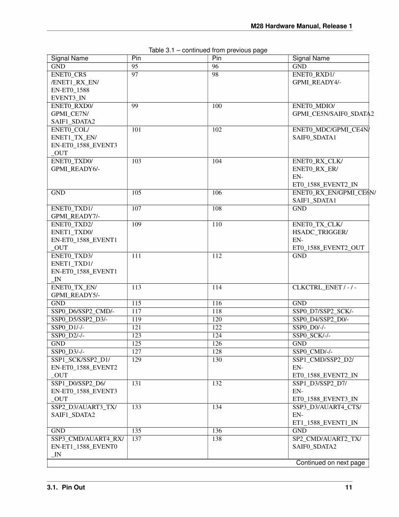
Table 3.1 – continued from previous pageSignal Name Pin Pin Signal NameGND 95 96 GNDENET0_CRS/ENET1_RX_EN/EN-ET0_1588EVENT3_IN
97 98 ENET0_RXD1/GPMI_READY4/-
ENET0_RXD0/GPMI_CE7N/SAIF1_SDATA2
99 100 ENET0_MDIO/GPMI_CE5N/SAIF0_SDATA2
ENET0_COL/ENET1_TX_EN/EN-ET0_1588_EVENT3_OUT
101 102 ENET0_MDC/GPMI_CE4N/SAIF0_SDATA1
ENET0_TXD0/GPMI_READY6/-
103 104 ENET0_RX_CLK/ENET0_RX_ER/EN-ET0_1588_EVENT2_IN
GND 105 106 ENET0_RX_EN/GPMI_CE6N/SAIF1_SDATA1
ENET0_TXD1/GPMI_READY7/-
107 108 GND
ENET0_TXD2/ENET1_TXD0/EN-ET0_1588_EVENT1_OUT
109 110 ENET0_TX_CLK/HSADC_TRIGGER/EN-ET0_1588_EVENT2_OUT
ENET0_TXD3/ENET1_TXD1/EN-ET0_1588_EVENT1_IN
111 112 GND
ENET0_TX_EN/GPMI_READY5/-
113 114 CLKCTRL_ENET / - / -
GND 115 116 GNDSSP0_D6/SSP2_CMD/- 117 118 SSP0_D7/SSP2_SCK/-SSP0_D5/SSP2_D3/- 119 120 SSP0_D4/SSP2_D0/-SSP0_D1/-/- 121 122 SSP0_D0/-/-SSP0_D2/-/- 123 124 SSP0_SCK/-/-GND 125 126 GNDSSP0_D3/-/- 127 128 SSP0_CMD/-/-SSP1_SCK/SSP2_D1/EN-ET0_1588_EVENT2_OUT
129 130 SSP1_CMD/SSP2_D2/EN-ET0_1588_EVENT2_IN
SSP1_D0/SSP2_D6/EN-ET0_1588_EVENT3_OUT
131 132 SSP1_D3/SSP2_D7/EN-ET0_1588_EVENT3_IN
SSP2_D3/AUART3_TX/SAIF1_SDATA2
133 134 SSP3_D3/AUART4_CTS/EN-ET1_1588_EVENT1_IN
GND 135 136 GNDSSP3_CMD/AUART4_RX/EN-ET1_1588_EVENT0_IN
137 138 SP2_CMD/AUART2_TX/SAIF0_SDATA2
Continued on next page
3.1. Pin Out 11
M28 Hardware Manual, Release 1
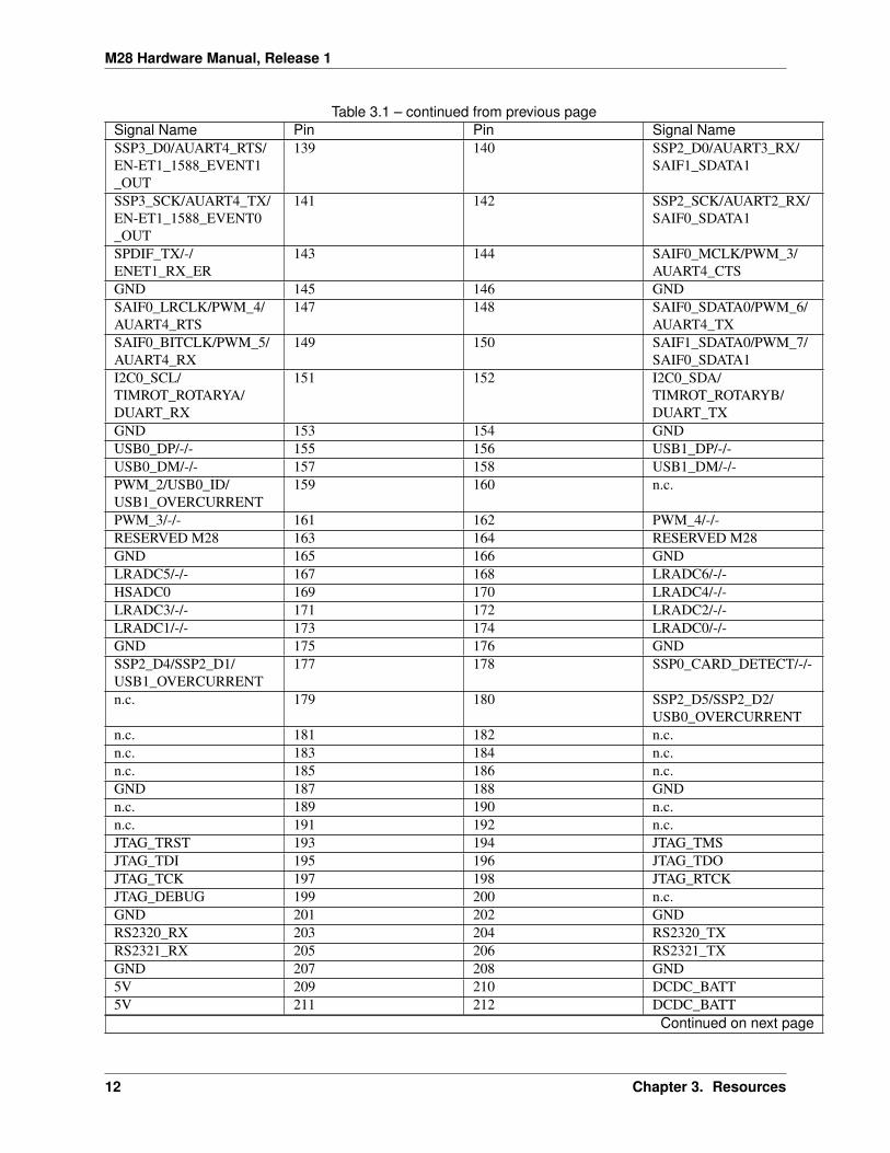
Table 3.1 – continued from previous pageSignal Name Pin Pin Signal NameSSP3_D0/AUART4_RTS/EN-ET1_1588_EVENT1_OUT
139 140 SSP2_D0/AUART3_RX/SAIF1_SDATA1
SSP3_SCK/AUART4_TX/EN-ET1_1588_EVENT0_OUT
141 142 SSP2_SCK/AUART2_RX/SAIF0_SDATA1
SPDIF_TX/-/ENET1_RX_ER
143 144 SAIF0_MCLK/PWM_3/AUART4_CTS
GND 145 146 GNDSAIF0_LRCLK/PWM_4/AUART4_RTS
147 148 SAIF0_SDATA0/PWM_6/AUART4_TX
SAIF0_BITCLK/PWM_5/AUART4_RX
149 150 SAIF1_SDATA0/PWM_7/SAIF0_SDATA1
I2C0_SCL/TIMROT_ROTARYA/DUART_RX
151 152 I2C0_SDA/TIMROT_ROTARYB/DUART_TX
GND 153 154 GNDUSB0_DP/-/- 155 156 USB1_DP/-/-USB0_DM/-/- 157 158 USB1_DM/-/-PWM_2/USB0_ID/USB1_OVERCURRENT
159 160 n.c.
PWM_3/-/- 161 162 PWM_4/-/-RESERVED M28 163 164 RESERVED M28GND 165 166 GNDLRADC5/-/- 167 168 LRADC6/-/-HSADC0 169 170 LRADC4/-/-LRADC3/-/- 171 172 LRADC2/-/-LRADC1/-/- 173 174 LRADC0/-/-GND 175 176 GNDSSP2_D4/SSP2_D1/USB1_OVERCURRENT
177 178 SSP0_CARD_DETECT/-/-
n.c. 179 180 SSP2_D5/SSP2_D2/USB0_OVERCURRENT
n.c. 181 182 n.c.n.c. 183 184 n.c.n.c. 185 186 n.c.GND 187 188 GNDn.c. 189 190 n.c.n.c. 191 192 n.c.JTAG_TRST 193 194 JTAG_TMSJTAG_TDI 195 196 JTAG_TDOJTAG_TCK 197 198 JTAG_RTCKJTAG_DEBUG 199 200 n.c.GND 201 202 GNDRS2320_RX 203 204 RS2320_TXRS2321_RX 205 206 RS2321_TXGND 207 208 GND5V 209 210 DCDC_BATT5V 211 212 DCDC_BATT
Continued on next page
12 Chapter 3. Resources
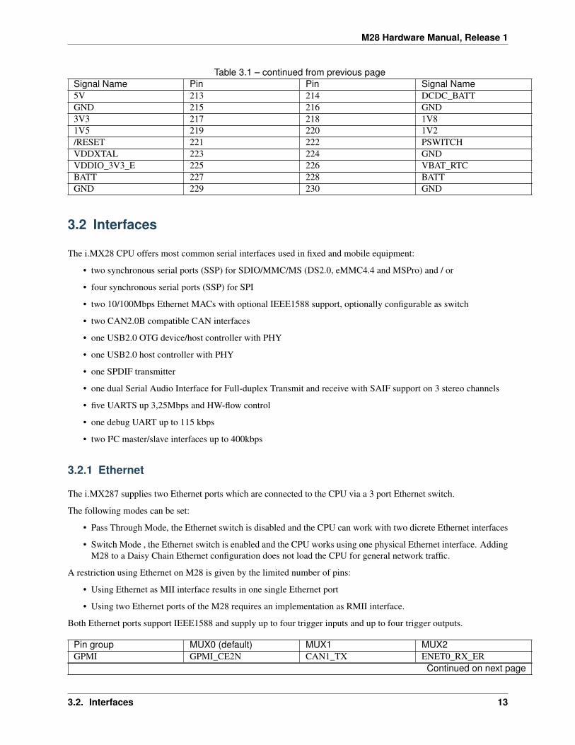
M28 Hardware Manual, Release 1
Table 3.1 – continued from previous pageSignal Name Pin Pin Signal Name5V 213 214 DCDC_BATTGND 215 216 GND3V3 217 218 1V81V5 219 220 1V2/RESET 221 222 PSWITCHVDDXTAL 223 224 GNDVDDIO_3V3_E 225 226 VBAT_RTCBATT 227 228 BATTGND 229 230 GND
3.2 Interfaces
The i.MX28 CPU offers most common serial interfaces used in fixed and mobile equipment:
• two synchronous serial ports (SSP) for SDIO/MMC/MS (DS2.0, eMMC4.4 and MSPro) and / or
• four synchronous serial ports (SSP) for SPI
• two 10/100Mbps Ethernet MACs with optional IEEE1588 support, optionally configurable as switch
• two CAN2.0B compatible CAN interfaces
• one USB2.0 OTG device/host controller with PHY
• one USB2.0 host controller with PHY
• one SPDIF transmitter
• one dual Serial Audio Interface for Full-duplex Transmit and receive with SAIF support on 3 stereo channels
• five UARTS up 3,25Mbps and HW-flow control
• one debug UART up to 115 kbps
• two I²C master/slave interfaces up to 400kbps
3.2.1 Ethernet
The i.MX287 supplies two Ethernet ports which are connected to the CPU via a 3 port Ethernet switch.
The following modes can be set:
• Pass Through Mode, the Ethernet switch is disabled and the CPU can work with two dicrete Ethernet interfaces
• Switch Mode , the Ethernet switch is enabled and the CPU works using one physical Ethernet interface. AddingM28 to a Daisy Chain Ethernet configuration does not load the CPU for general network traffic.
A restriction using Ethernet on M28 is given by the limited number of pins:
• Using Ethernet as MII interface results in one single Ethernet port
• Using two Ethernet ports of the M28 requires an implementation as RMII interface.
Both Ethernet ports support IEEE1588 and supply up to four trigger inputs and up to four trigger outputs.
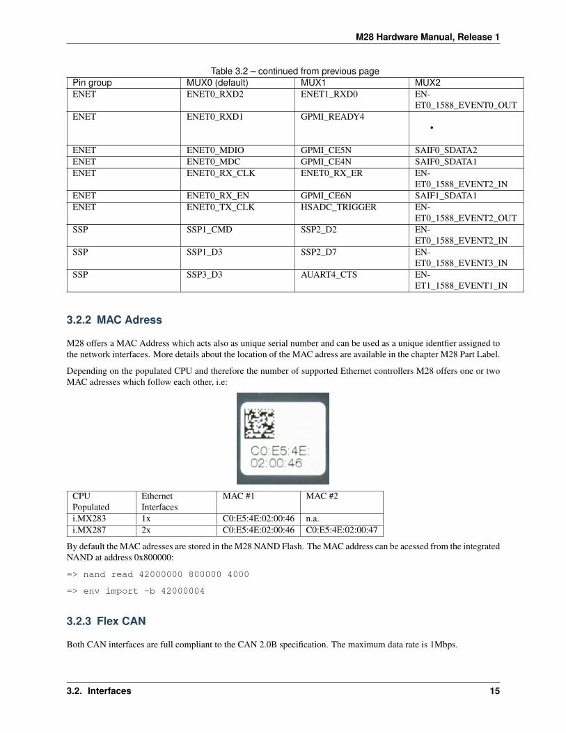
Pin group MUX0 (default) MUX1 MUX2GPMI GPMI_CE2N CAN1_TX ENET0_RX_ER
Continued on next page
3.2. Interfaces 13
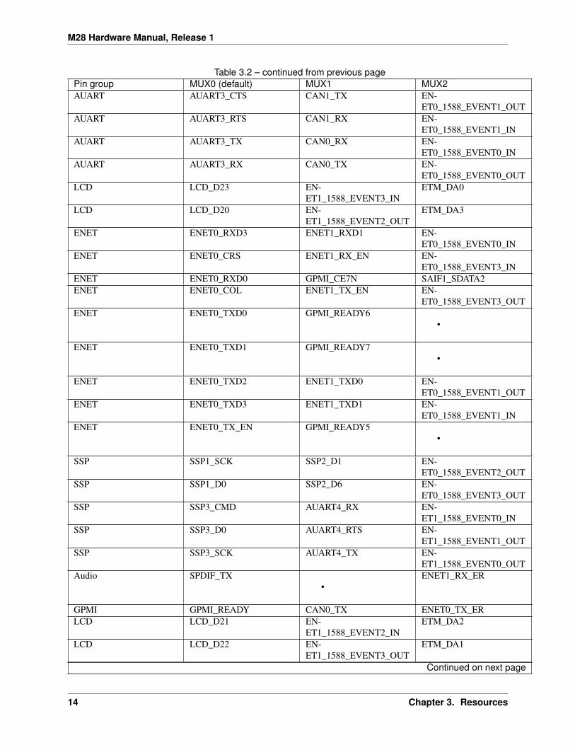
M28 Hardware Manual, Release 1
Table 3.2 – continued from previous pagePin group MUX0 (default) MUX1 MUX2AUART AUART3_CTS CAN1_TX EN-
ET0_1588_EVENT1_OUTAUART AUART3_RTS CAN1_RX EN-
ET0_1588_EVENT1_INAUART AUART3_TX CAN0_RX EN-
ET0_1588_EVENT0_INAUART AUART3_RX CAN0_TX EN-
ET0_1588_EVENT0_OUTLCD LCD_D23 EN-
ET1_1588_EVENT3_INETM_DA0
LCD LCD_D20 EN-ET1_1588_EVENT2_OUT
ETM_DA3
ENET ENET0_RXD3 ENET1_RXD1 EN-ET0_1588_EVENT0_IN
ENET ENET0_CRS ENET1_RX_EN EN-ET0_1588_EVENT3_IN
ENET ENET0_RXD0 GPMI_CE7N SAIF1_SDATA2ENET ENET0_COL ENET1_TX_EN EN-
ET0_1588_EVENT3_OUTENET ENET0_TXD0 GPMI_READY6
•
ENET ENET0_TXD1 GPMI_READY7•
ENET ENET0_TXD2 ENET1_TXD0 EN-ET0_1588_EVENT1_OUT
ENET ENET0_TXD3 ENET1_TXD1 EN-ET0_1588_EVENT1_IN
ENET ENET0_TX_EN GPMI_READY5•
SSP SSP1_SCK SSP2_D1 EN-ET0_1588_EVENT2_OUT
SSP SSP1_D0 SSP2_D6 EN-ET0_1588_EVENT3_OUT
SSP SSP3_CMD AUART4_RX EN-ET1_1588_EVENT0_IN
SSP SSP3_D0 AUART4_RTS EN-ET1_1588_EVENT1_OUT
SSP SSP3_SCK AUART4_TX EN-ET1_1588_EVENT0_OUT
Audio SPDIF_TX•
ENET1_RX_ER
GPMI GPMI_READY CAN0_TX ENET0_TX_ERLCD LCD_D21 EN-
ET1_1588_EVENT2_INETM_DA2
LCD LCD_D22 EN-ET1_1588_EVENT3_OUT
ETM_DA1
Continued on next page
14 Chapter 3. Resources
M28 Hardware Manual, Release 1
Table 3.2 – continued from previous pagePin group MUX0 (default) MUX1 MUX2ENET ENET0_RXD2 ENET1_RXD0 EN-
ET0_1588_EVENT0_OUTENET ENET0_RXD1 GPMI_READY4
•
ENET ENET0_MDIO GPMI_CE5N SAIF0_SDATA2ENET ENET0_MDC GPMI_CE4N SAIF0_SDATA1ENET ENET0_RX_CLK ENET0_RX_ER EN-
ET0_1588_EVENT2_INENET ENET0_RX_EN GPMI_CE6N SAIF1_SDATA1ENET ENET0_TX_CLK HSADC_TRIGGER EN-
ET0_1588_EVENT2_OUTSSP SSP1_CMD SSP2_D2 EN-
ET0_1588_EVENT2_INSSP SSP1_D3 SSP2_D7 EN-
ET0_1588_EVENT3_INSSP SSP3_D3 AUART4_CTS EN-
ET1_1588_EVENT1_IN
3.2.2 MAC Adress
M28 offers a MAC Address which acts also as unique serial number and can be used as a unique identfier assigned tothe network interfaces. More details about the location of the MAC adress are available in the chapter M28 Part Label.
Depending on the populated CPU and therefore the number of supported Ethernet controllers M28 offers one or twoMAC adresses which follow each other, i.e:
CPUPopulated
EthernetInterfaces
MAC #1 MAC #2
i.MX283 1x C0:E5:4E:02:00:46 n.a.i.MX287 2x C0:E5:4E:02:00:46 C0:E5:4E:02:00:47
By default the MAC adresses are stored in the M28 NAND Flash. The MAC address can be acessed from the integratedNAND at address 0x800000:
=> nand read 42000000 800000 4000
=> env import -b 42000004
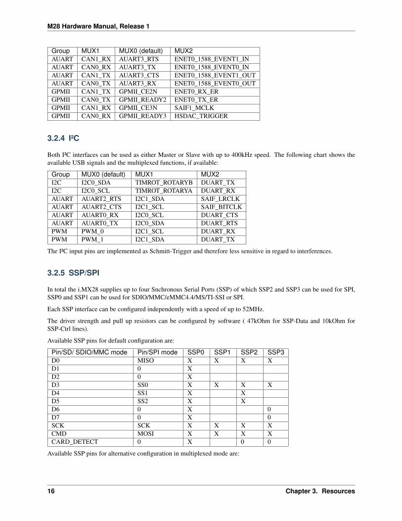
3.2.3 Flex CAN
Both CAN interfaces are full compliant to the CAN 2.0B specification. The maximum data rate is 1Mbps.
3.2. Interfaces 15
M28 Hardware Manual, Release 1
Group MUX1 MUX0 (default) MUX2AUART CAN1_RX AUART3_RTS ENET0_1588_EVENT1_INAUART CAN0_RX AUART3_TX ENET0_1588_EVENT0_INAUART CAN1_TX AUART3_CTS ENET0_1588_EVENT1_OUTAUART CAN0_TX AUART3_RX ENET0_1588_EVENT0_OUTGPMII CAN1_TX GPMII_CE2N ENET0_RX_ERGPMII CAN0_TX GPMII_READY2 ENET0_TX_ERGPMII CAN1_RX GPMII_CE3N SAIF1_MCLKGPMII CAN0_RX GPMII_READY3 HSDAC_TRIGGER
3.2.4 I²C
Both I²C interfaces can be used as either Master or Slave with up to 400kHz speed. The following chart shows theavailable USB signals and the multiplexed functions, if available:
Group MUX0 (default) MUX1 MUX2I2C I2C0_SDA TIMROT_ROTARYB DUART_TXI2C I2C0_SCL TIMROT_ROTARYA DUART_RXAUART AUART2_RTS I2C1_SDA SAIF_LRCLKAUART AUART2_CTS I2C1_SCL SAIF_BITCLKAUART AUART0_RX I2C0_SCL DUART_CTSAUART AUART0_TX I2C0_SDA DUART_RTSPWM PWM_0 I2C1_SCL DUART_RXPWM PWM_1 I2C1_SDA DUART_TX
The I²C input pins are implemented as Schmitt-Trigger and therefore less sensitive in regard to interferences.
3.2.5 SSP/SPI
In total the i.MX28 supplies up to four Snchronous Serial Ports (SSP) of which SSP2 and SSP3 can be used for SPI,SSP0 and SSP1 can be used for SDIO/MMC/eMMC4.4/MS/TI-SSI or SPI.
Each SSP interface can be configured independently with a speed of up to 52MHz.
The driver strength and pull up resistors can be configured by software ( 47kOhm for SSP-Data and 10kOhm forSSP-Ctrl lines).
Available SSP pins for default configuration are:
Pin/SD/ SDIO/MMC mode Pin/SPI mode SSP0 SSP1 SSP2 SSP3D0 MISO X X X XD1 0 XD2 0 XD3 SS0 X X X XD4 SS1 X XD5 SS2 X XD6 0 X 0D7 0 X 0SCK SCK X X X XCMD MOSI X X X XCARD_DETECT 0 X 0 0
Available SSP pins for alternative configuration in multiplexed mode are:
16 Chapter 3. Resources
M28 Hardware Manual, Release 1
Pin/SD/ SDIO/MMC mode Pin/SPI mode SSP0 SSP1 SSP2 SSP3D0 MISO X X XD1 X X XD2 X X XD3 SS0 X X XD4 SS1 X XD5 SS2 X XD6 0 X X 0D7 0 X X 0SCK SCK X X XCMD MOSI X X XCARD_DETECT 0 X 0 0
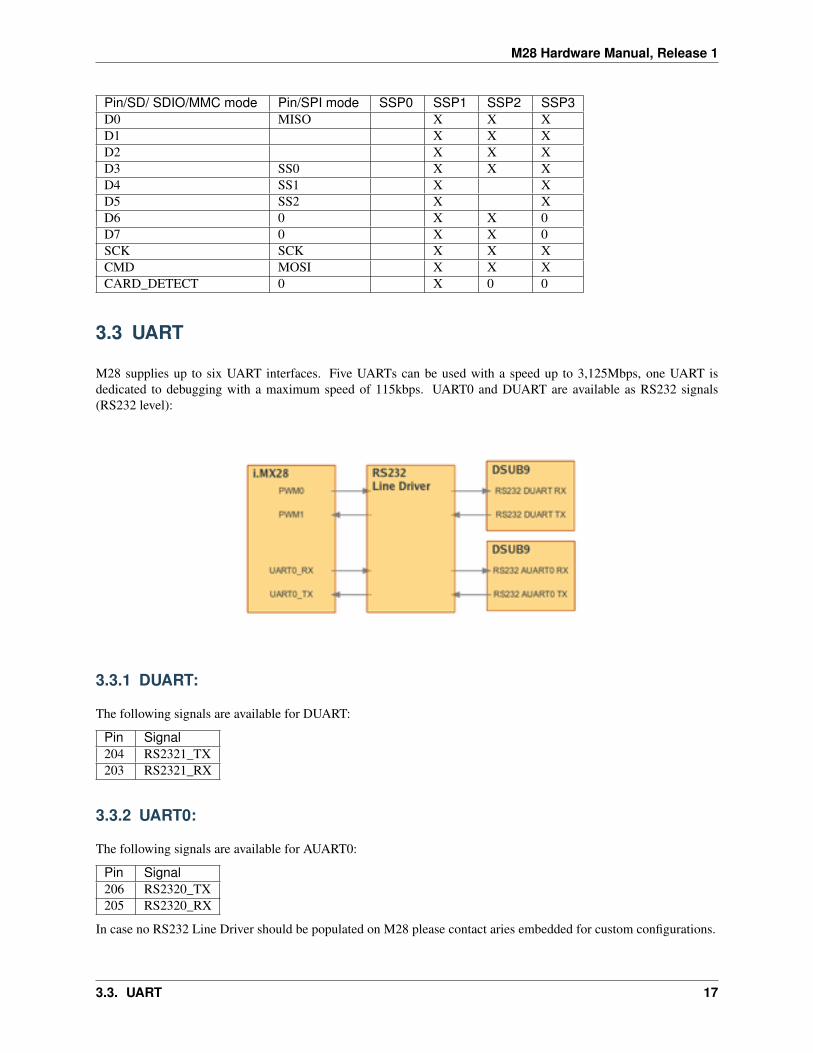
3.3 UART
M28 supplies up to six UART interfaces. Five UARTs can be used with a speed up to 3,125Mbps, one UART isdedicated to debugging with a maximum speed of 115kbps. UART0 and DUART are available as RS232 signals(RS232 level):
3.3.1 DUART:
The following signals are available for DUART:
Pin Signal204 RS2321_TX203 RS2321_RX
3.3.2 UART0:
The following signals are available for AUART0:
Pin Signal206 RS2320_TX205 RS2320_RX
In case no RS232 Line Driver should be populated on M28 please contact aries embedded for custom configurations.
3.3. UART 17
M28 Hardware Manual, Release 1
3.4 USB
The i.MX28 CPU supports two high speed USB controllers with integrated PHY. USB0 can be used asOTG/device/host, USB1 can be used as host. Both USB controllers support Full-Speed or High-Speed mode, Low-Speed mode is not supported.
The following chart shows the available USB signals and the multiplexed functions, if available:
Pin group MUX0 (default) MUX1 MUX2AUART AUART1_CTS USB0_OVERCURRENT TIMROT_ROTARYAAUART AUART1_RTS USB0_ID TIMROT_ROTARYBGPMI GPMI_READY0 SSP1_CARD_DETECT USB0_IDPWM PWM_2 USB0_ID USB1_OVERCURRENTSSP SSP2_D4 SSP2_D1 USB1_OVERCURRENTSSP SSP2_D5 SSP2_D2 USB0_OVERCURRENTUSB USB0DP 0 0USB USB0DM 0 0USB USB1DP 0 0USB USB1DM 0 0
3.5 Analogue
3.5.1 HSADC
The High Speed 12 bit A/D Converter supplies a maximum sampling rate of 2MSps and can be synchronized with thePWM outputs.
Also triggering the HSADC by software or an external signal via HSADC_Trigger is possible.
3.5.2 LRADC
The i.MX28 supplies a Low Resolution 12 bit A/D Converter (LRADC) with a maximum sampling rate of 428kHzand a precision of 1,5% which can be improved to 0,5% by calibrating the bandgap reference.
The LRADC is multiplexed by a 16 channel analogue multiplexer:
• channel 0 for an external temperature diode or as an input for the keyboard matrix
• channel 1-6 as external 4/5- wire touch screen controller, input impedance 1MOhm, touch screen impedances200Ohms . . . 50kOhm.
• channel 1 alternatively as input for the keyboard matrix
• channel 7 for measurement of the battery voltage
• channel 8-9 for internal temperature measurement, 2% accuracy
• channel 10 for internal VDDIO
• channel 11 is reserved for internal analogue tests
• channel 12 for internal VDDA
• channel 13 for internal VDDD
• channel 14 for internal bandgap reference
• channel 15 for internal VDD5V
18 Chapter 3. Resources
M28 Hardware Manual, Release 1
The input range is defined for the range of 0V...1,85V.
3.6 Audio
3.6.1 SAIF
The i.MX28 CPU supplies a SAIF interface which can be used for recording and playback. Due to the versatileconfiguration options most differnet analogue codecs can be used. The following options can be selected:
• 3, 4 or 5 wire interface connection to the codec
• 16 bit or 24 bit Stereo digital audio PCM interface
• half-duplex for recording and playback
• 2 channels Stereo / Mono
• 4 channels Stereo / Surround
• 6 channels Stereo / Surround / Center / LFE
• flexible frame format, i.e. I2S, SIF (i.e. for DSP), left/right oriented frames and other options
• bit clock (BITCLK) and left / right clock (LRCLK) as master or slave
• master clock (MCLK) in a range of 32 times up 512 times of the audio sampling rate for synchronisation withexternal codecs / DACs
• free configurable sampling rate in the range of 8kHz to 192kHz
The i.MX28 supplies two SAIF interfaces which can be used with the following contraints:
• one SAIF as Tx-master, the other SAIF as Rx-slave, BITCLK and LRCLK supplied by master
• one SAIF as Rx-master, the other SAIF as Rx-slave, BITCLK and LRCLK supplied by master
• both SAIF as Rx-slave, BITCLK and LRCLK supplied by external codec
• both SAIF as master, BITCLK and LRCLK supplied by respective master
• one SAIF in random configuration
Most SAIF pins are multiplexed with other functional blocks so that restrictions may have to be considered.
3.6.2 SPDIF
The SPDIF interface (Sony-Philips Digital Interface Format according IEC-60958) supplied by the i.MX28 can beused as transmitter with a sampling rate of 32 kHz, 44.1 kHz or 48 kHz as well as twice as much of these frequencies.Also a pre-emphasis of 50/15µs can be configured.
3.7 GPIO
Almost all non-EMI digital pins of the i.MX28 CPU have a general-purpose input/output (GPIO) mode and used
• as input or output
• with an output driver strength of 4mA, 8mA or 12mA
• based on an input-/output voltage of 1,8V or 3,3V
3.6. Audio 19
M28 Hardware Manual, Release 1
• with internal pull up resistors for a couple of pins (10k or 47k resistor, according to pin
• as interrupt input triggered by level or rising/falling edge
3.8 GPMI
The GPMI General-Purpose Media Interface is not available on M28 in the default configuration. For customizedconfiguration please contact aries embedded.
3.9 Keypad
LRADC0 and LRADC1 can be used to implement a keypad matrix with maximum 8x8 keys. For de-bouncing and therecognition of a pressed button a threshold detection with interrupt capabilities is available.
3.10 PWM
The I.MX28 supplies up to 8 PWM outputs. PWM3 and PWM4 are available in any case, all other PWM blocks areavailable in multiplexed modes:
Group |MUX0 (default) MUX1 MUX2AUART AUART1_RX SSP2_CARD_DETECT PWM0AUART AUART1_TX SSP3_CARD_DETECT PWM1PWM PWM_0 I2C1_SCL DUART_RXPWM PWM_1 I2C1_SDA DUART_TXPWM PWM_2 USB0_ID USB1_OVERCURRENTPWM PWM_3 0 0PWM PWM_4 0 0SAIF SAIF0_BITCLK PWM_5 AUART4_RXSAIF SAIF0_LRCLK PWM_4 AUART4_RTSSAIF SAIF0_MCLK PWM_3 AUART4_CTSSAIF SAIF0_DATA0 PWM_6 AUART4_TXSAIF SAIF1_DATA0 PWM_7 SAIF0_DATA1
Typical application examples for the PWM outputs are LED and backlight control or simple motor control applications.
Each channel can be set up individually for cycle duration, high time, low time and phasing.
The PWM unit can be used on three different modes covering the following frequency ranges:
Mode FrequencyXTAL Clock 0 - 24 MHzHSADC Clock 0 - 32 MHzMATT = Multichip Attachment Mode 32kHz or 24 MHz fixed
For XTAL Clock and HSADC Clock mode the following parameters can be configured:
• input frequency divider 1, 2, 4, 8, 16, 64, 256 and 1024
• number of clock cycles for a PWM cycle
• number of clock cycles for the active time of the PWM cycle
• number of clock cycles for the inactive time of the PWM cycle
20 Chapter 3. Resources

M28 Hardware Manual, Release 1
• polarity of the PWM output in active / inactive status
3.11 Rotary Decoder
A rotary encode can be connected directly to the M28 module. The internal circuitry of the CPU supports
• debouncing by programmable oversampling
• automatic direction recognition
• relativ or absolute counting
As input pins the dedicated rotary decoder pins or the eight PWM pins can be used.
The following multiplexing is applied for this block:
Group MUX0 (default) MUX1 MUX2AUART AUART1_CTS USB0_OVERCURRENT TIMROT_ROTARYAAUART AUART1_RTS USB0_ID TIMROT_ROTARYBI2C I2C0_SDA TIMROT_ROTARYB DUART_TXI2C I2C0_SCL TIMROT_ROTARYA DUART_RX
3.12 Timer
On M28 up to four 32 bit timers are available. The timer input pins are multiplexed with the eight PWM pins or therotary decoder.
Alternatively the 32kHz clock can be used for the timer counter. It can be divided by 1, 4, 8 or 32.
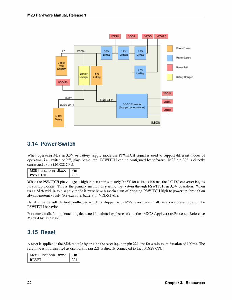
3.13 Power Supply
The power supply of the i.MX28 CPU is shown in the figure below. All main components of the M28 embeddedmodule like i.e. DDR2 RAM and NAND Flash are powered by the i.MX28 on-chip power management unit.
More information on the i.MX28 Power Management Unit are available on Freescale’s i.MX28 Website in applicationnote AN4199.
3.11. Rotary Decoder 21
M28 Hardware Manual, Release 1
3.14 Power Switch
When operating M28 in 3,3V or battery supply mode the PSWITCH signal is used to support different modes ofoperation, i.e. switch on/off, play, pause, etc. PSWITCH can be configured by software. M28 pin 222 is directlyconnected to the i.MX28 CPU.
M28 Functional Block PinPSWITCH 222
When the PSWITCH pin voltage is higher than approximately 0,65V for a time >100 ms, the DC-DC converter beginsits startup routine. This is the primary method of starting the system through PSWITCH in 3,3V operation. Whenusing M28 with in this supply mode it must have a mechanism of bringing PSWITCH high to power up through analways-present supply (for example, battery or VDDXTAL).
Usually the default U-Boot bootloader which is shipped with M28 takes care of all necessary presettings for thePSWITCH behavior.
For more details for implementing dedicated functionality please refer to the i.MX28 Applications Processor ReferenceManual by Freescale.
3.15 Reset
A reset is applied to the M28 module by driving the reset input on pin 221 low for a minimum duration of 100ms. Thereset line is implemented as open drain, pin 221 is directly connected to the i.MX28 CPU.
M28 Functional Block PinRESET 221
22 Chapter 3. Resources
M28 Hardware Manual, Release 1
3.16 Supply Modes
M28 can be connected to different kind of supplies:
• a lithium ion accumulator which can also be charged by the module, supply range 2.6V...4.24V
• 3.3V, supply range 2.6V...4.24V
-a USB connection or generic 5V supply, supply range 4.75V...5.25V
Sup-ply
ModeSupply
Voltage Supply Pins
5V 4.75...5.25V209, 211, 213Bat-tery
2.6V...4.24V210, 212, 214
3.3V 2.6V...4.24V210, 212, 214GND GND 1, 2, 13, 14, 23, 24, 35, 36, 45, 46, 55, 56, 65, 66, 75, 76, 85, 86, 95, 96,
105, 108, 112, 115, 116, 125, 126, 135, 136, 145, 146, 153, 154, 165,166,175, 176, 187, 188, 201, 202, 207, 208, 215, 216, 224, 229, 230
3.16. Supply Modes 23