Embed Size (px)
Citation preview
Comprehensive report on achievements of the JST PRESTO Project
“ Materials and Processes for Next-Generation Innovative Devices”
Katsuaki SatoJapan Science and Technology Agency (JST)
Objectives
This presentation is a report on the achievements of the JST-PRESTO project “Materials and Processes for Next Generation Innovative Devices”, which started on October 2007 and ended on March 2013.I dedicated myself as a Research Supervisor of this Project.
2
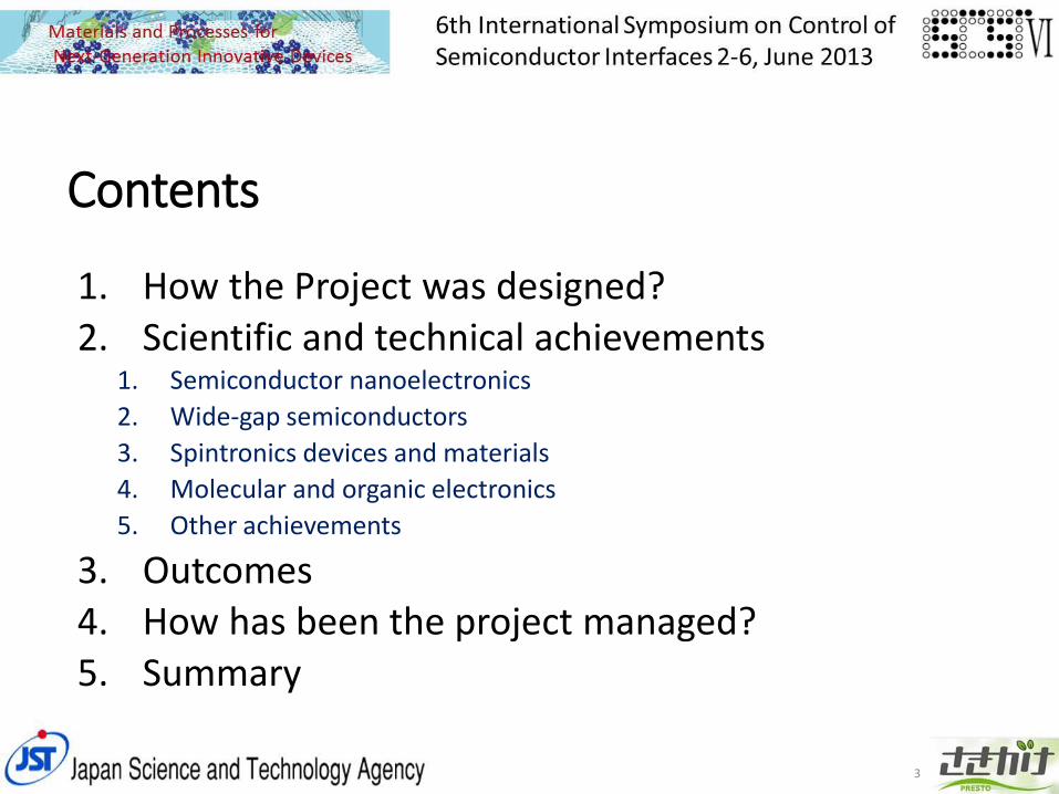
Contents
1. How the Project was designed?2. Scientific and technical achievements
1. Semiconductor nanoelectronics
2. Wide-gap semiconductors
3. Spintronics devices and materials
4. Molecular and organic electronics
5. Other achievements
3. Outcomes4. How has been the project managed?5. Summary
3
How the Project was designed?
Introduction
4
Background of the Project• Silicon crystals used for semiconductor integrated circuits
represented by CMOS are regarded as the most basic material supporting today’s living.
• Semiconductor manufacturing technologies are indivisibly related to nanotechnology, since they become more and more sophisticated as exemplified by the fact that the manufacturing accuracy of the CMOS micro-processing plunges into the nanometer range.
• Consequently the limit of 22 nm half pitch is approaching, which in turn requires device development based on new concepts and/or new principles beyond conventional silicon CMOS technologies.
5
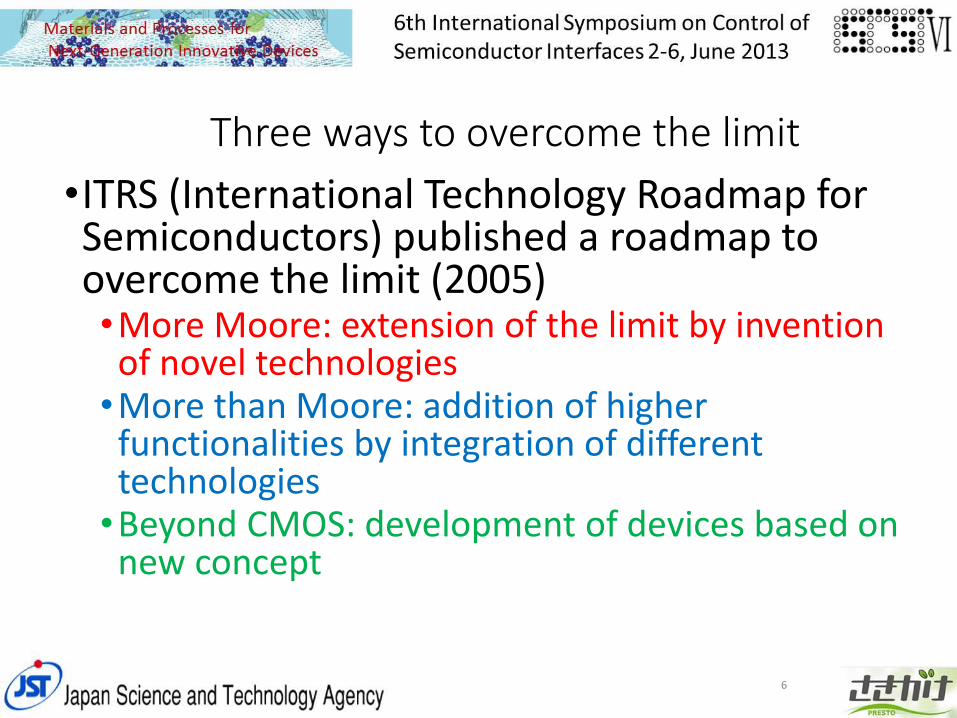
Three ways to overcome the limit
•ITRS (International Technology Roadmap for Semiconductors) published a roadmap to overcome the limit (2005) •More Moore: extension of the limit by invention
of novel technologies•More than Moore: addition of higher
functionalities by integration of different technologies
•Beyond CMOS: development of devices based on new concept
6
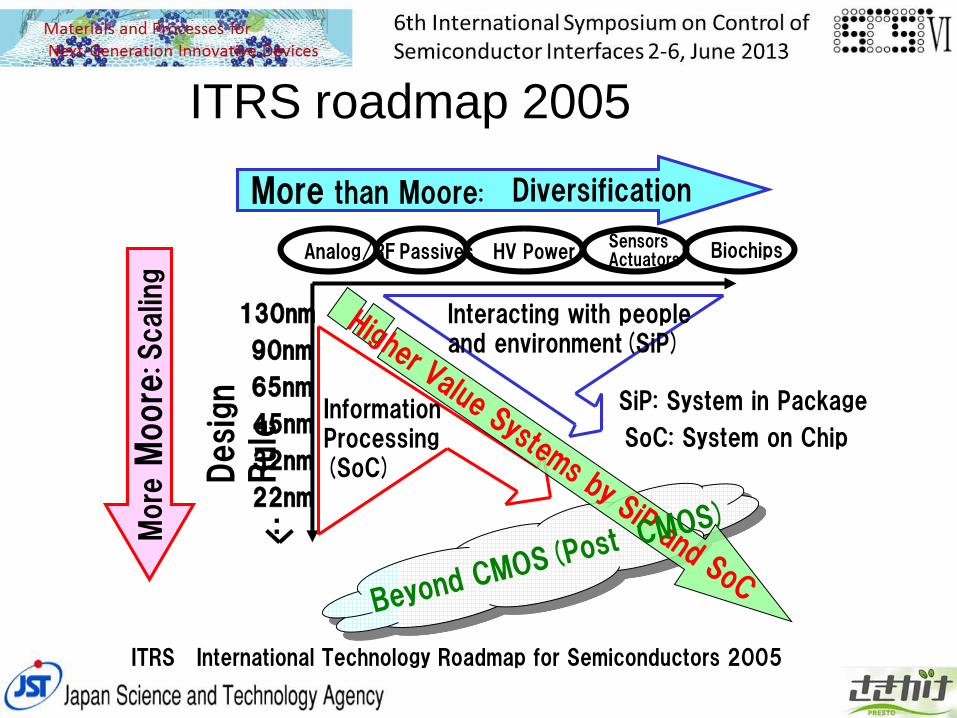
ITRS International Technology Roadmap for Semiconductors 2005
ITRS roadmap 2005
Analog/RF Passives HV PowerSensorsActuators Biochips
22nm
32nm
45nm
65nm
90nm
130nm
Scalin
gM
ore
Moore
:
More than Moore: Diversification
・・
Interacting with people and environment(SiP)
SiP: System in Package
SoC: System on ChipInformation Processing (SoC)D
esi
gn
Rule
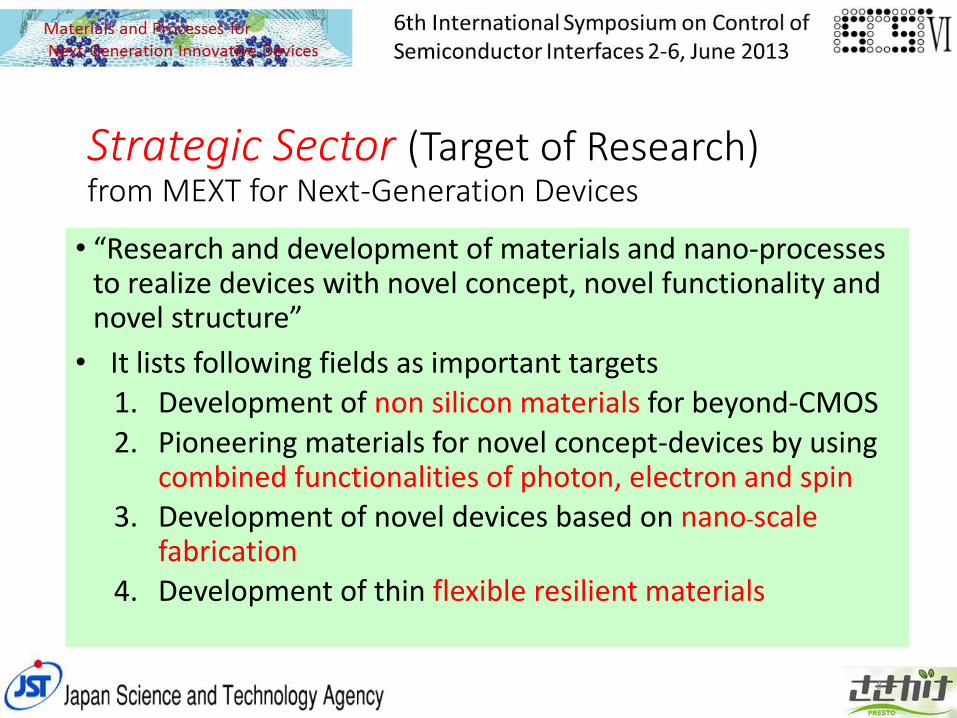
Strategic Sector (Target of Research) from MEXT for Next-Generation Devices
• “Research and development of materials and nano-processes to realize devices with novel concept, novel functionality and novel structure”
• It lists following fields as important targets1. Development of non silicon materials for beyond-CMOS2. Pioneering materials for novel concept-devices by using
combined functionalities of photon, electron and spin3. Development of novel devices based on nano-scale
fabrication4. Development of thin flexible resilient materials
8
METI Nanoelectronics project(Non-Si channel, Nanowire, XMOS)
9
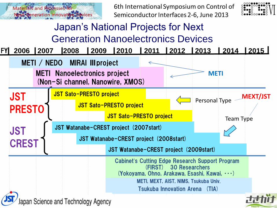
Japan’s National Projects for Next
Generation Nanoelectronics Devices2006 2007 2008 2009 2010 2011 2012 2013 2014 2015
METI / NEDO MIRAI Ⅲproject
Cabinet’s Cutting Edge Research Support Program(FIRST) 30 Researchers
(Yokoyama, Ohno, Arakawa, Esashi, Kawai, ・・・)
METI, MEXT, AIST, NIMS, Tsukuba Univ.
Tsukuba Innovation Arena (TIA)
FY
JST Watanabe-CREST project (2007start)
JST Watanabe-CREST project (2008start)
JST Watanabe-CREST project (2009start)
JST
CREST
JST
PRESTO
JST Sato-PRESTO project
JST Sato-PRESTO project
JST Sato-PRESTO project
Personal Type
Team Type
METI
MEXT/JST
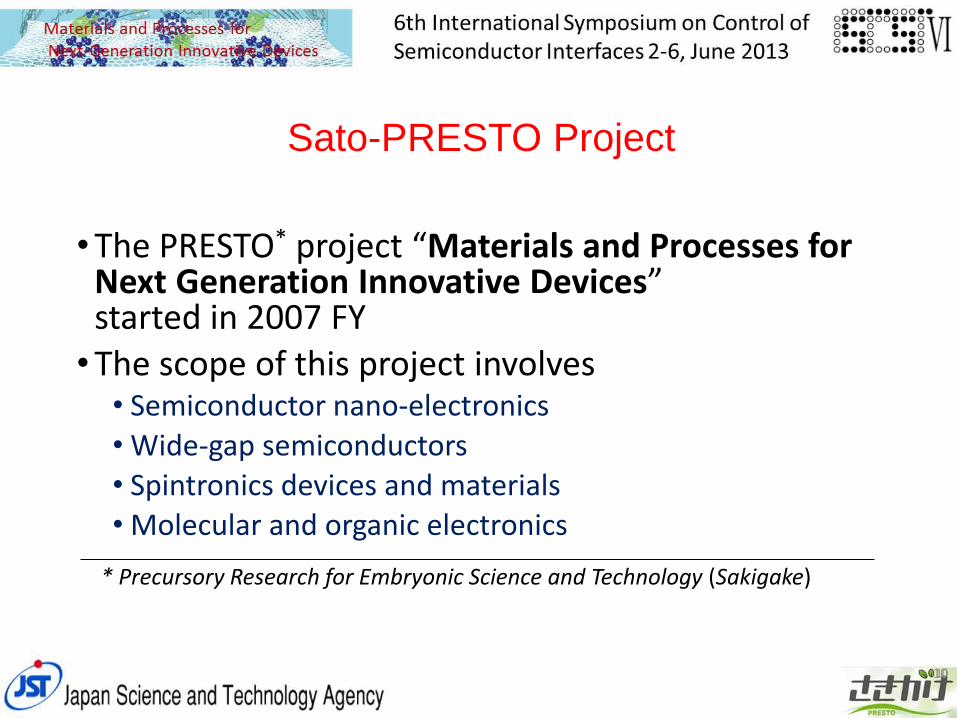
Sato-PRESTO Project
• The PRESTO* project “Materials and Processes for Next Generation Innovative Devices” started in 2007 FY
• The scope of this project involves• Semiconductor nano-electronics• Wide-gap semiconductors• Spintronics devices and materials• Molecular and organic electronics
* Precursory Research for Embryonic Science and Technology (Sakigake)
1010
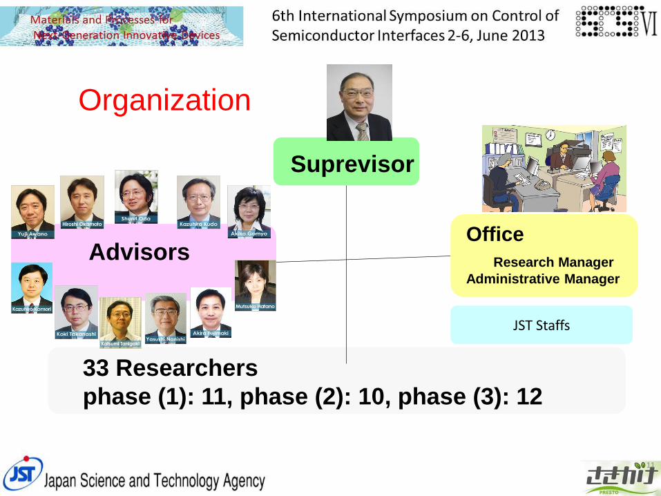
Organization
Suprevisor
Advisors
33 Researchers
phase (1): 11, phase (2): 10, phase (3): 12
JST Staffs
Office
Research Manager
Administrative Manager
11
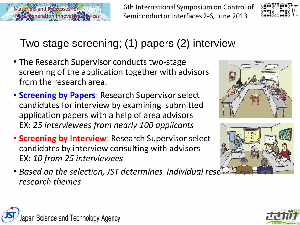
Two stage screening; (1) papers (2) interview
• The Research Supervisor conducts two-stage screening of the application together with advisors from the research area.
• Screening by Papers: Research Supervisor selectcandidates for interview by examining submitted application papers with a help of area advisorsEX: 25 interviewees from nearly 100 applicants
• Screening by Interview: Research Supervisor selectcandidates by interview consulting with advisorsEX: 10 from 25 interviewees
• Based on the selection, JST determines individual researchers and research themes
12
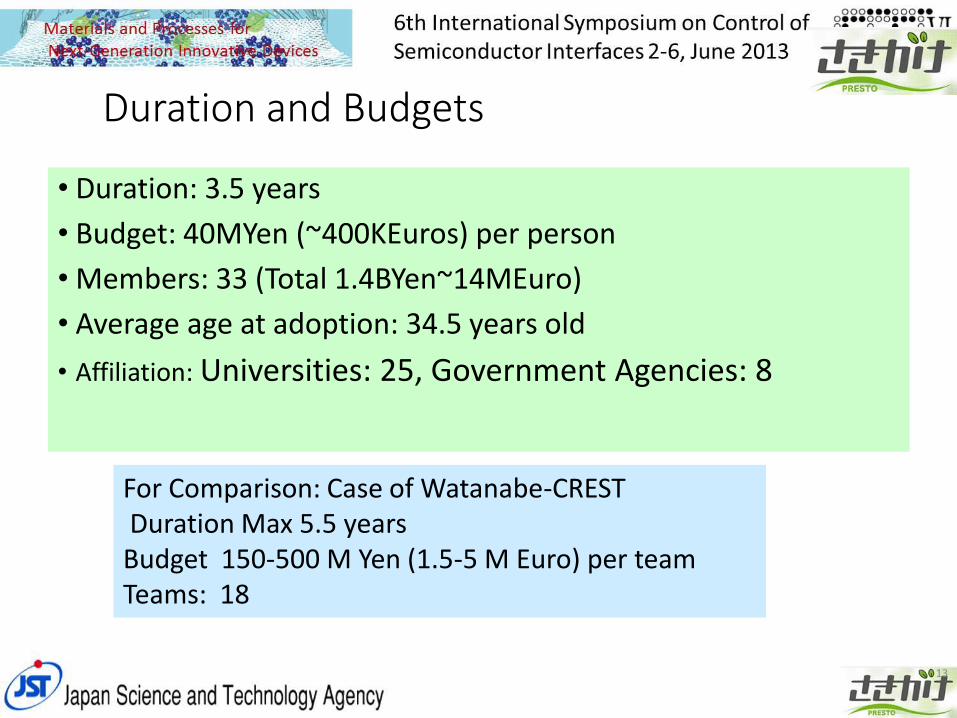
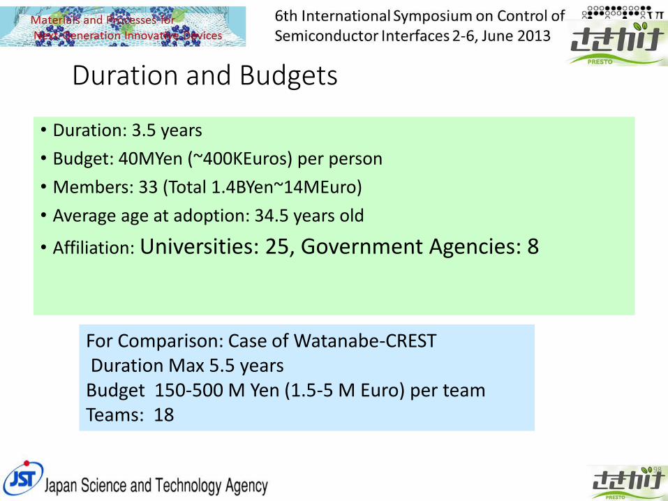
Duration and Budgets
• Duration: 3.5 years
• Budget: 40MYen (~400KEuros) per person
• Members: 33 (Total 1.4BYen~14MEuro)
• Average age at adoption: 34.5 years old
• Affiliation: Universities: 25, Government Agencies: 8
For Comparison: Case of Watanabe-CRESTDuration Max 5.5 years
Budget 150-500 M Yen (1.5-5 M Euro) per teamTeams: 18
13
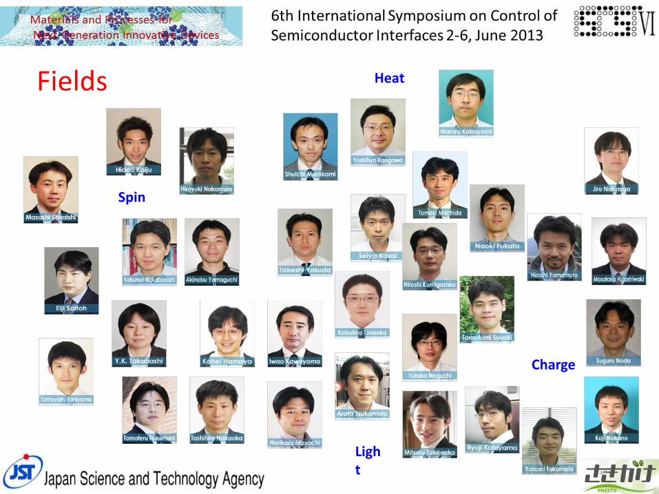
Fields
Charge
Heat
Spin
Light 14
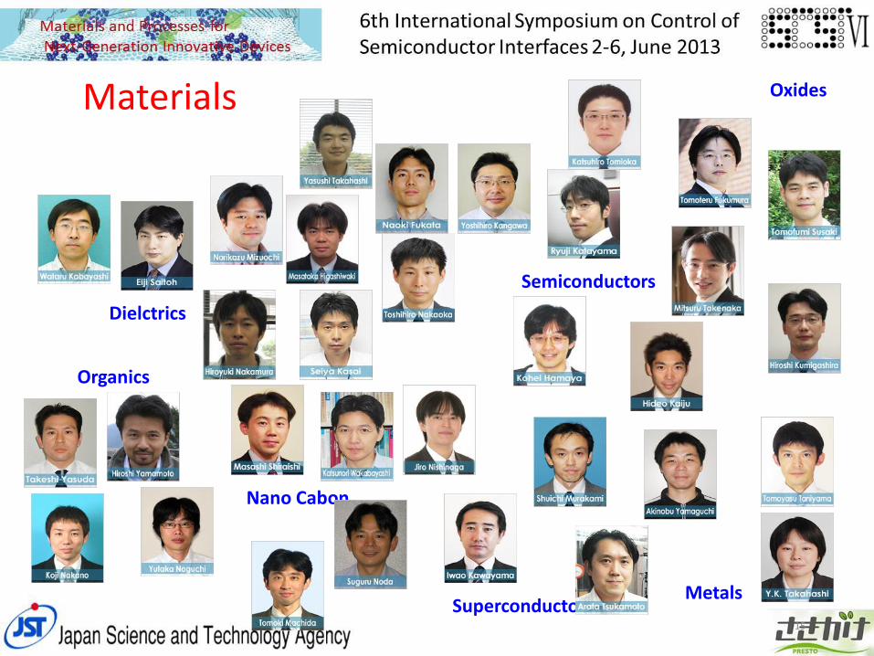
Materials
Semiconductors
Metals
Organics
Dielctrics
Superconductor
Oxides
Nano Cabon
15
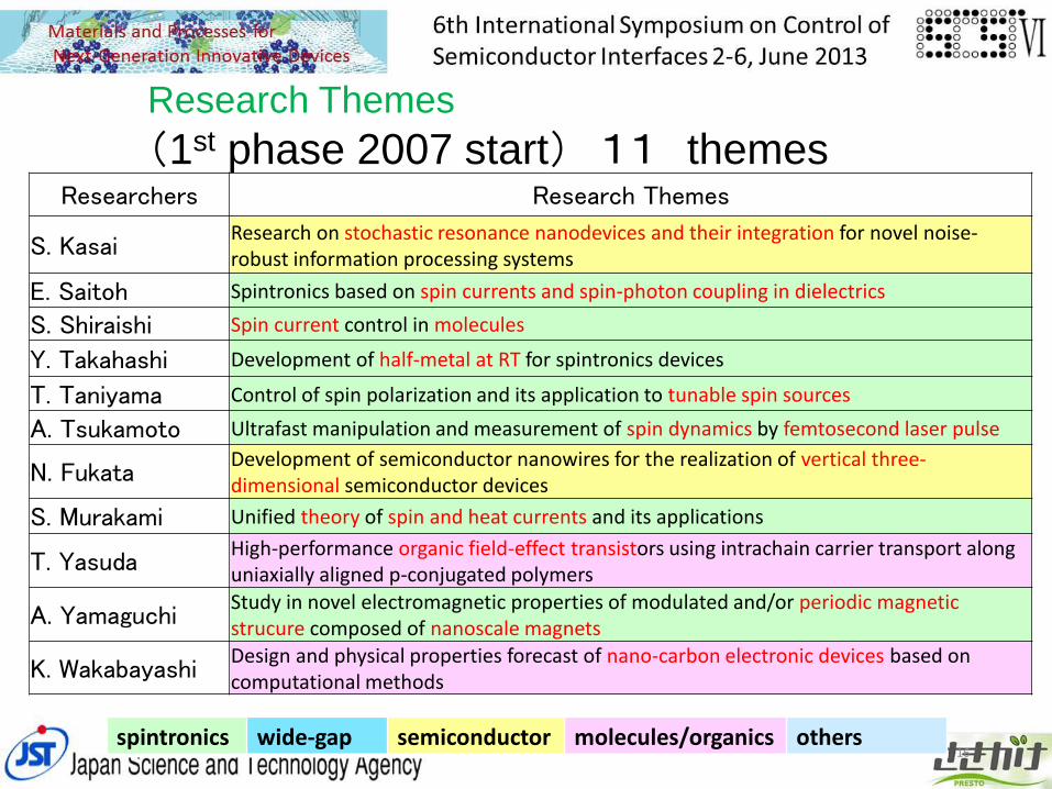
Research Themes
(1st phase 2007 start) 11 themesResearchers Research Themes
S. KasaiResearch on stochastic resonance nanodevices and their integration for novel noise-robust information processing systems
E. Saitoh Spintronics based on spin currents and spin-photon coupling in dielectrics
S. Shiraishi Spin current control in molecules
Y. Takahashi Development of half-metal at RT for spintronics devices
T. Taniyama Control of spin polarization and its application to tunable spin sources
A. Tsukamoto Ultrafast manipulation and measurement of spin dynamics by femtosecond laser pulse
N. FukataDevelopment of semiconductor nanowires for the realization of vertical three-dimensional semiconductor devices
S. Murakami Unified theory of spin and heat currents and its applications
T. YasudaHigh-performance organic field-effect transistors using intrachain carrier transport along uniaxially aligned p-conjugated polymers
A. YamaguchiStudy in novel electromagnetic properties of modulated and/or periodic magnetic strucure composed of nanoscale magnets
K. WakabayashiDesign and physical properties forecast of nano-carbon electronic devices based on computational methods
spintronics wide-gap semiconductor molecules/organics others16
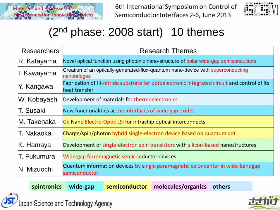
(2nd phase: 2008 start) 10 themes
Researchers Research Themes
R. Katayama Novel optical function using photonic nano-structure of polar wide-gap semiconductors
I. KawayamaCreation of an optically-generated-flux-quantum nano-device with superconducting
nanobridges
Y. KangawaFabrication of III-nitride substrate for optoelectronic integrated circuit and control of its heat transfer
W. Kobayashi Development of materials for thermoelectronics
T. Susaki New functionalities at the interfaces of wide-gap oxides
M. Takenaka Ge Nano Electro-Optic LSI for intrachip optical interconnects
T. Nakaoka Charge/spin/photon hybrid single-electron device based on quantum dot
K. Hamaya Development of single-electron spin transistors with silicon-based nanostructures
T. Fukumura Wide-gap ferromagnetic semiconductor devices
N. MizuochiQuantum information devices by single paramagnetic color center in wide-bandgapsemiconductor
spintronics wide-gap semiconductor molecules/organics others
17
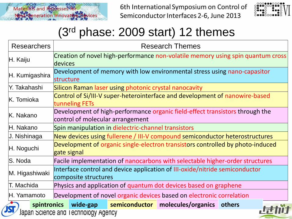
(3rd phase: 2009 start) 12 themesResearchers Research Themes
H. KaijuCreation of novel high-performance non-volatile memory using spin quantum crossdevices
H. KumigashiraDevelopment of memory with low environmental stress using nano-capasitorstructure
Y. Takahashi Silicon Raman laser using photonic crystal nanocavity
K. TomiokaControl of Si/III-V super-heterointerface and development of nanowire-based tunneling FETs
K. NakanoDevelopment of high-performance organic field-effect transistors through the control of molecular arrangement
H. Nakano Spin manipulation in dielectric-channel transistorsJ. Nishinaga New devices using fullerene / III-V compound semiconductor heterostructures
H. NoguchiDevelopment of organic single-electron transistors controlled by photo-induced gate signal
S. Noda Facile implementation of nanocarbons with selectable higher-order structures
M. HigashiwakiInterface control and device application of III-oxide/nitride semiconductor composite structures
T. Machida Physics and application of quantum dot devices based on graphene
H. Yamamoto Development of novel organic devices based on electronic correlation
spintronics wide-gap semiconductor molecules/organics others18
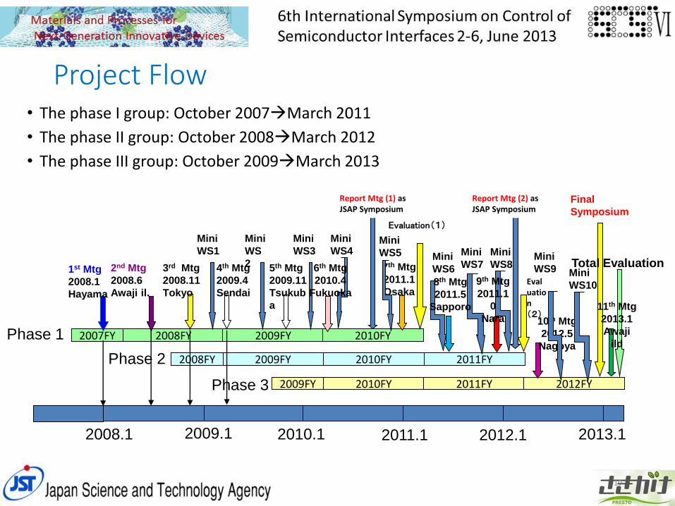
Project Flow• The phase I group: October 2007March 2011
• The phase II group: October 2008March 2012
• The phase III group: October 2009March 2013
2008FY 2009FY 2010FY
2009FY 2010FY 2011FY
2010FY 2011FY 2012FY
2007FY
2008FY
2009FY
Phase 1
Phase 2
Phase 3
1st Mtg
2008.1
Hayama
2nd Mtg
2008.6
Awaji il.
2008.1 2009.1 2010.1 2011.1 2012.1 2013.1
3rd Mtg
2008.11
Tokyo
4th Mtg
2009.4
Sendai
Report Mtg (1) as JSAP Symposium
Mini
WS1
Total Evaluation
Evaluation(1)
Evaluation(2)
Final
Symposium
Mini
WS
2 5th Mtg
2009.11
Tsukub
a
Mini
WS3
Mini
WS4
6th Mtg
2010.4
Fukuoka
7th Mtg
2011.1
Osaka
Mini
WS5
Report Mtg (2) as JSAP Symposium
Mini
WS6
Mini
WS7
Mini
WS8
10th Mtg
2012.5
Nagoya
9th Mtg
2011.1
0
Nara
8th Mtg
2011.5
Sapporo 11th Mtg
2013.1
Awaji
ild
19
Mini
WS9 Mini
WS10
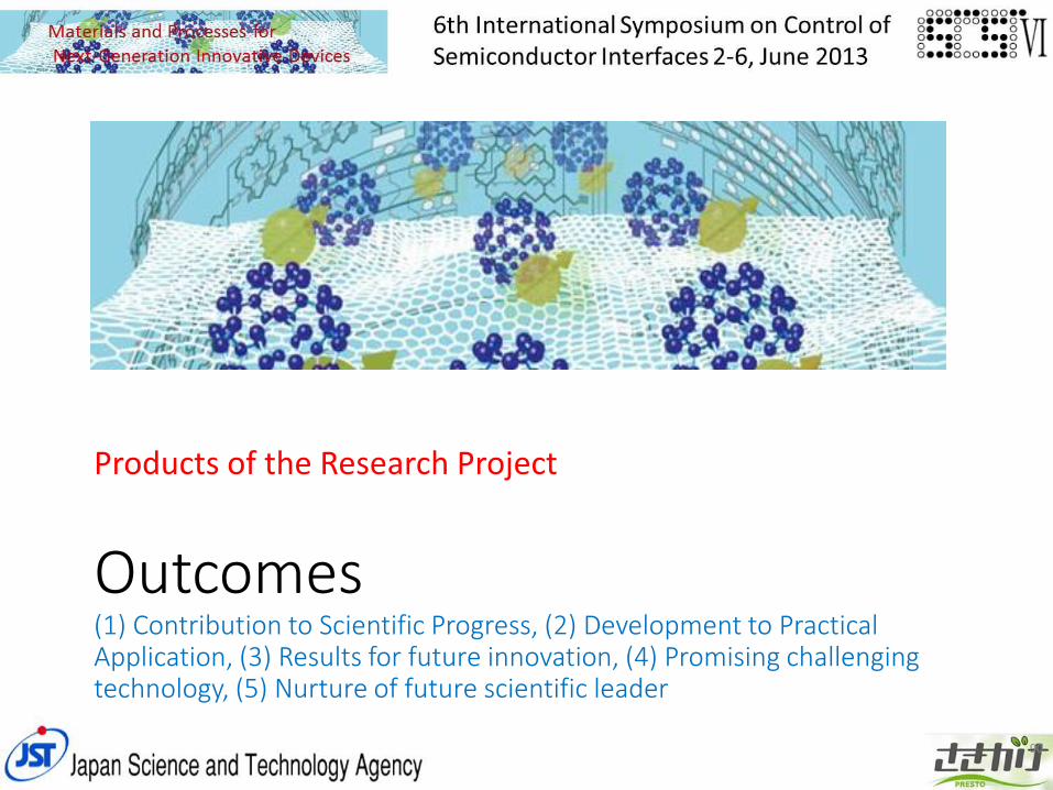
Products of the Research Project
20
Scientific and technical achievements
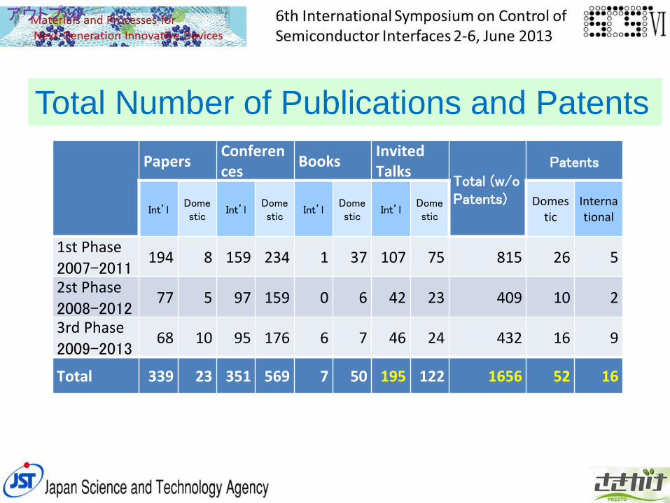
Total Number of Publications and Patents
PapersConferences
BooksInvited Talks
Total (w/oPatents)
Patents
Int’lDomestic
Int’lDomestic
Int’lDomestic
Int’lDomestic
Domestic
International
1st Phase
2007-2011194 8 159 234 1 37 107 75 815 26 5
2st Phase
2008-201277 5 97 159 0 6 42 23 409 10 2
3rd Phase
2009-201368 10 95 176 6 7 46 24 432 16 9
Total 339 23 351 569 7 50 195 122 1656 52 16
アウトプット
21
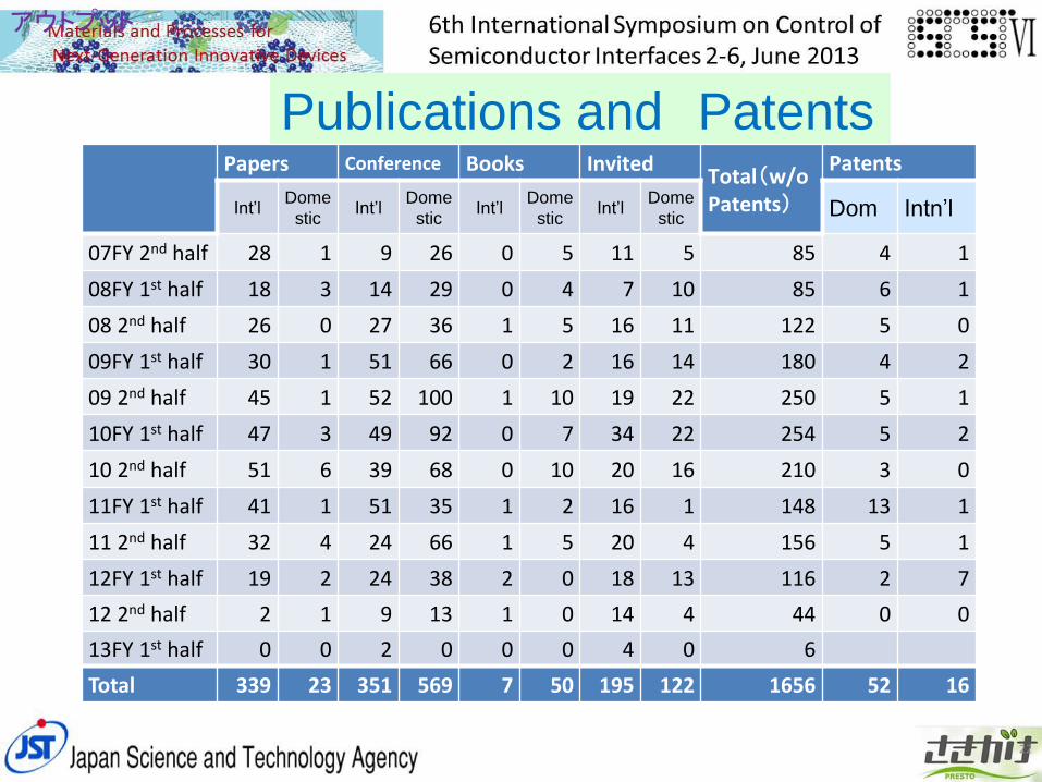
Publications and PatentsPapers Conference Books Invited
Total(w/o Patents)
Patents
Int’lDome
sticInt’l
Dome
sticInt’l
Dome
sticInt’l
Dome
sticDom Intn’l
07FY 2nd half 28 1 9 26 0 5 11 5 85 4 1
08FY 1st half 18 3 14 29 0 4 7 10 85 6 1
08 2nd half 26 0 27 36 1 5 16 11 122 5 0
09FY 1st half 30 1 51 66 0 2 16 14 180 4 2
09 2nd half 45 1 52 100 1 10 19 22 250 5 1
10FY 1st half 47 3 49 92 0 7 34 22 254 5 2
10 2nd half 51 6 39 68 0 10 20 16 210 3 0
11FY 1st half 41 1 51 35 1 2 16 1 148 13 1
11 2nd half 32 4 24 66 1 5 20 4 156 5 1
12FY 1st half 19 2 24 38 2 0 18 13 116 2 7
12 2nd half 2 1 9 13 1 0 14 4 44 0 0
13FY 1st half 0 0 2 0 0 0 4 0 6
Total 339 23 351 569 7 50 195 122 1656 52 16
アウトプット
22
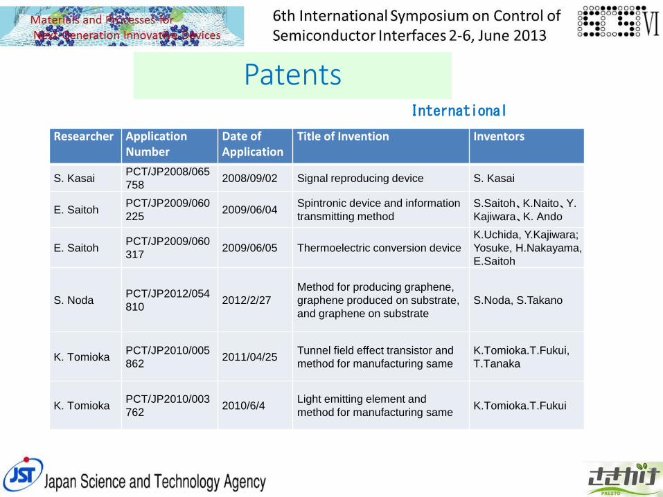
PatentsInternational
23
Researcher Application Number
Date of Application
Title of Invention Inventors
S. KasaiPCT/JP2008/065
7582008/09/02 Signal reproducing device S. Kasai
E. SaitohPCT/JP2009/060
2252009/06/04
Spintronic device and information
transmitting method
S.Saitoh、K.Naito、Y.
Kajiwara、K. Ando
E. SaitohPCT/JP2009/060
3172009/06/05 Thermoelectric conversion device
K.Uchida, Y.Kajiwara;
Yosuke, H.Nakayama,
E.Saitoh
S. NodaPCT/JP2012/054
8102012/2/27
Method for producing graphene,
graphene produced on substrate,
and graphene on substrate
S.Noda, S.Takano
K. TomiokaPCT/JP2010/005
8622011/04/25
Tunnel field effect transistor and
method for manufacturing same
K.Tomioka.T.Fukui,
T.Tanaka
K. TomiokaPCT/JP2010/003
7622010/6/4
Light emitting element and
method for manufacturing sameK.Tomioka.T.Fukui
Achievements
Semiconductor nanoelectronics
Wide-gap semiconductors
Spintronics devices and materials
Molecular and organic electronics
24
Semiconductor Nanoelectronics
Achievements
25
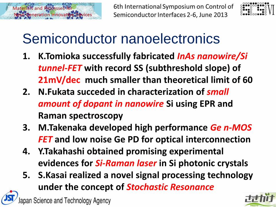
Semiconductor nanoelectronics1. K.Tomioka successfully fabricated InAs nanowire/Si
tunnel-FET with record SS (subthreshold slope) of 21mV/dec much smaller than theoretical limit of 60
2. N.Fukata succeded in characterization of small amount of dopant in nanowire Si using EPR and Raman spectroscopy
3. M.Takenaka developed high performance Ge n-MOS FET and low noise Ge PD for optical interconnection
4. Y.Takahashi obtained promising experimental evidences for Si-Raman laser in Si photonic crystals
5. S.Kasai realized a novel signal processing technology under the concept of Stochastic Resonance
26
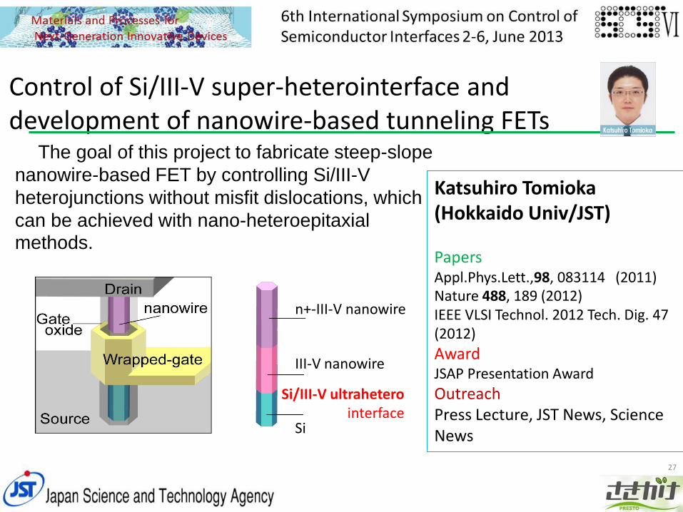
Control of Si/III-V super-heterointerface and development of nanowire-based tunneling FETs
Katsuhiro Tomioka(Hokkaido Univ/JST)
PapersAppl.Phys.Lett.,98, 083114 (2011)Nature 488, 189 (2012)IEEE VLSI Technol. 2012 Tech. Dig. 47 (2012)
AwardJSAP Presentation Award
OutreachPress Lecture, JST News, Science News
The goal of this project to fabricate steep-slope
nanowire-based FET by controlling Si/III-V
heterojunctions without misfit dislocations, which
can be achieved with nano-heteroepitaxialmethods.
n+-III-V nanowire
III-V nanowire
Si
Si/III-V ultraheterointerface
27
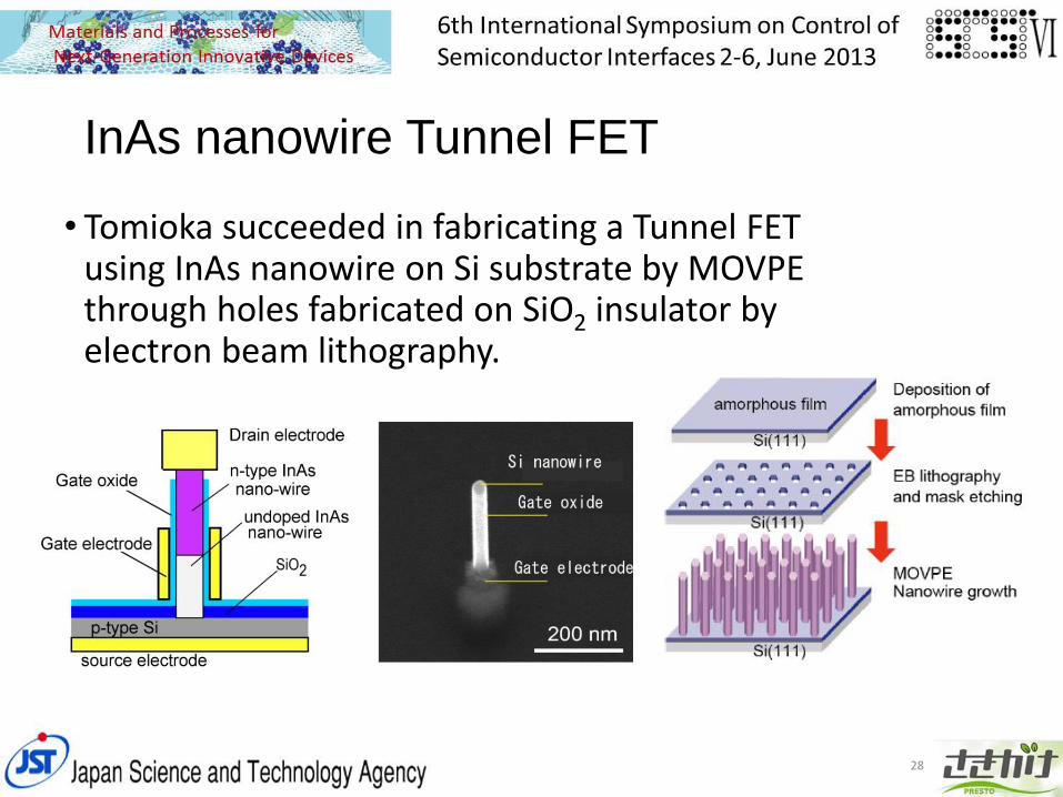
InAs nanowire Tunnel FET
• Tomioka succeeded in fabricating a Tunnel FET using InAs nanowire on Si substrate by MOVPE through holes fabricated on SiO2 insulator by electron beam lithography.
28
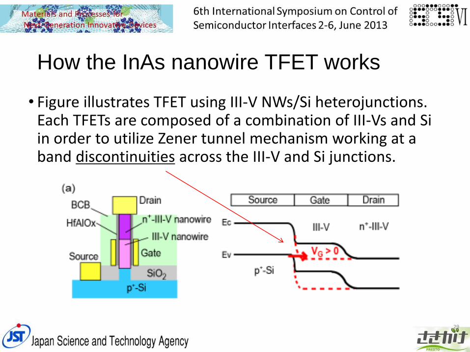
How the InAs nanowire TFET works
• Figure illustrates TFET using III-V NWs/Si heterojunctions. Each TFETs are composed of a combination of III-Vs and Si in order to utilize Zener tunnel mechanism working at a band discontinuities across the III-V and Si junctions.
29
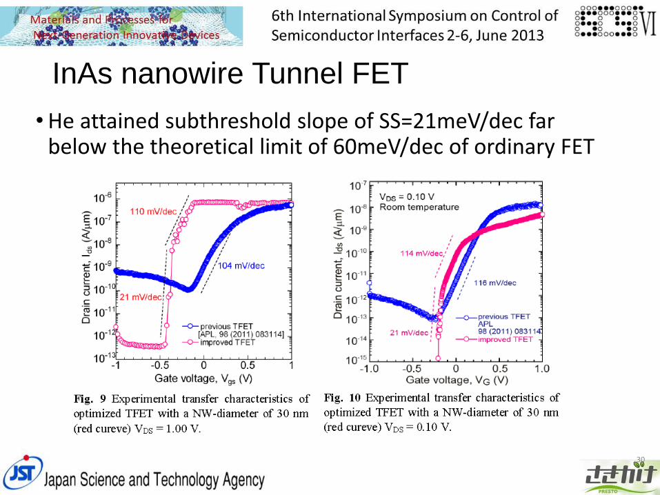
InAs nanowire Tunnel FET
• He attained subthreshold slope of SS=21meV/dec far below the theoretical limit of 60meV/dec of ordinary FET
30
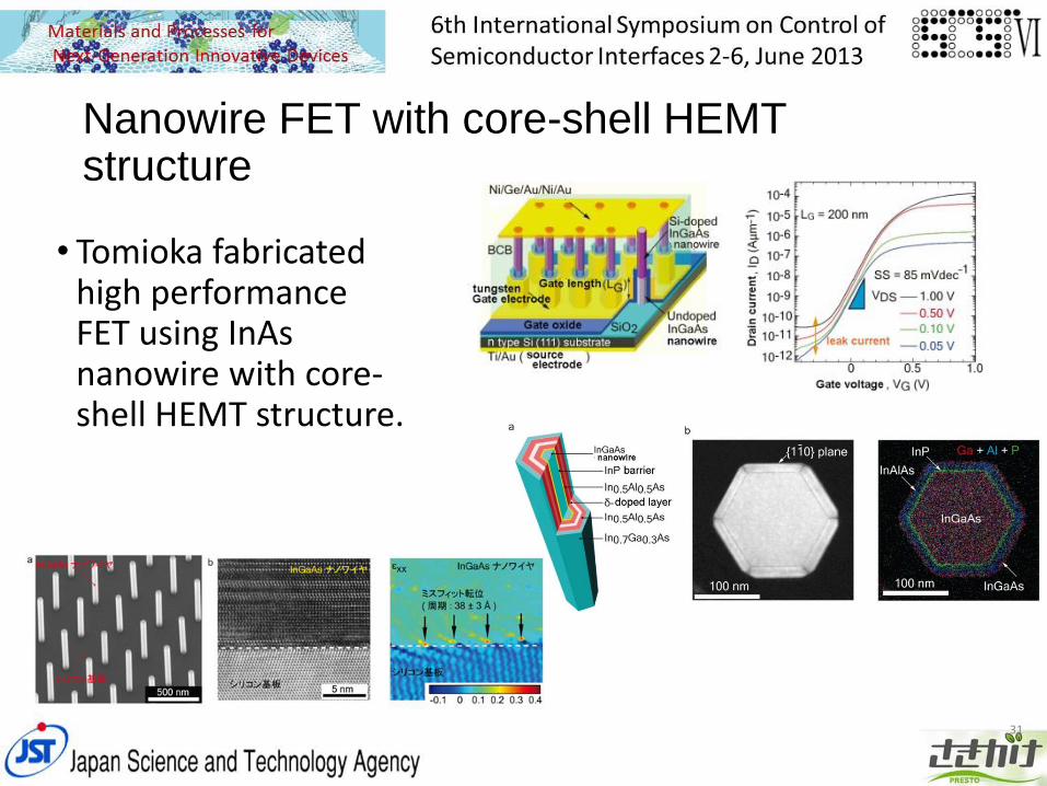
Nanowire FET with core-shell HEMT structure
• Tomioka fabricated high performance FET using InAsnanowire with core-shell HEMT structure.
31
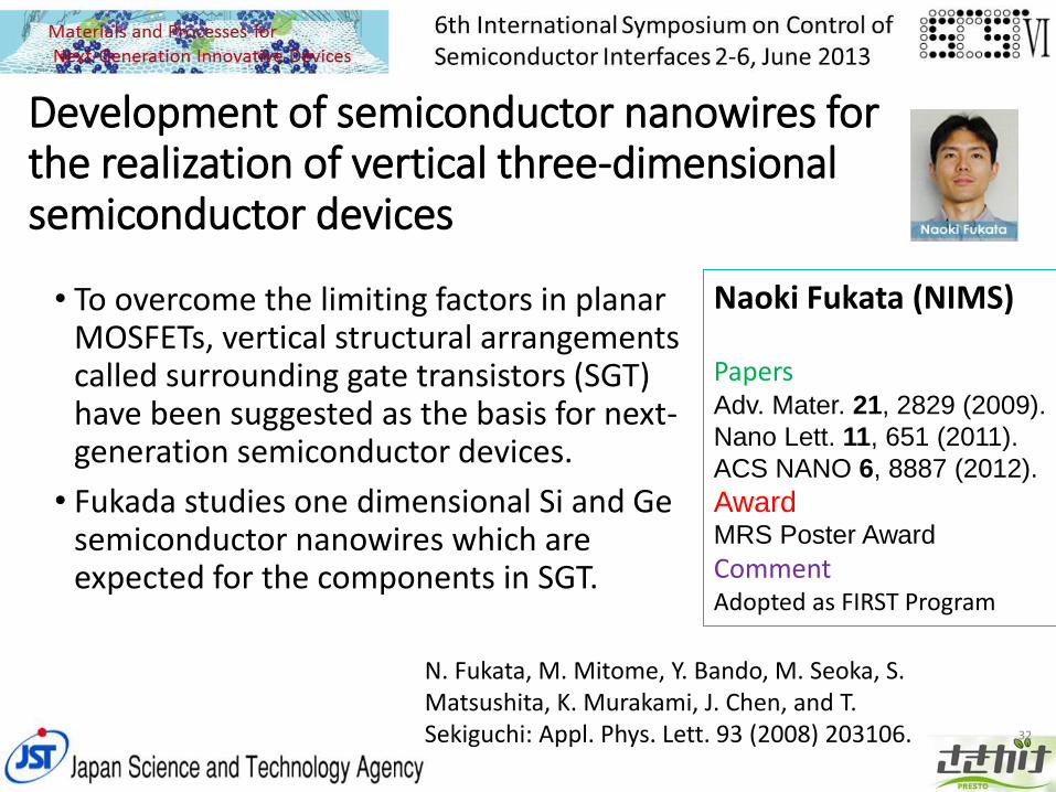
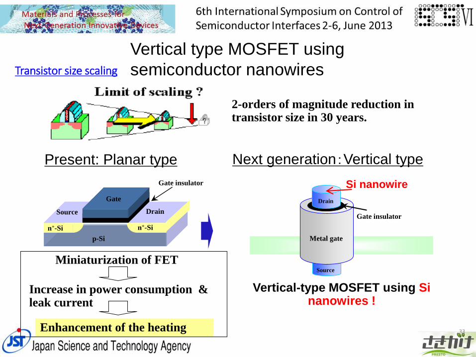
Development of semiconductor nanowires for the realization of vertical three-dimensional semiconductor devices
• To overcome the limiting factors in planar MOSFETs, vertical structural arrangements called surrounding gate transistors (SGT) have been suggested as the basis for next-generation semiconductor devices.
• Fukada studies one dimensional Si and Gesemiconductor nanowires which are expected for the components in SGT.
32
Naoki Fukata (NIMS)
PapersAdv. Mater. 21, 2829 (2009).
Nano Lett. 11, 651 (2011).
ACS NANO 6, 8887 (2012).
AwardMRS Poster Award
CommentAdopted as FIRST Program
N. Fukata, M. Mitome, Y. Bando, M. Seoka, S. Matsushita, K. Murakami, J. Chen, and T. Sekiguchi: Appl. Phys. Lett. 93 (2008) 203106.
Metal gate
Gate insulator
Drain
Source
Si nanowire
p-Si
n+-Si n+-Si
Gate
Gate insulator
Source Drain
Present: Planar type Next generation:Vertical type
Vertical-type MOSFET using Si nanowires !
2-orders of magnitude reduction in transistor size in 30 years.
Transistor size scaling
Enhancement of the heating
Miniaturization of FET
Increase in power consumption & leak current
33
Vertical type MOSFET using
semiconductor nanowires
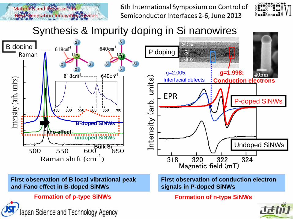
Synthesis & Impurity doping in Si nanowires
First observation of B local vibrational peak
and Fano effect in B-doped SiNWs
SiOx
Si
SiOxB doping
First observation of conduction electron
signals in P-doped SiNWs
g=1.998:
Conduction electrons
g=2.005:
Interfacial defects
Inte
nsi
ty (ar
b. u
nits)
324322320318Magnetic field (mT)
P-doped SiNWs
Undoped SiNWs
40nm
Inte
nsity
(arb
. uni
ts)
650600550500
Raman shift (cm-1
)
Bulk Si
B-doped SiNWs
undoped SiNWsFano effect
P doping
Formation of p-type SiNWs Formation of n-type SiNWs
EPR
Raman
34
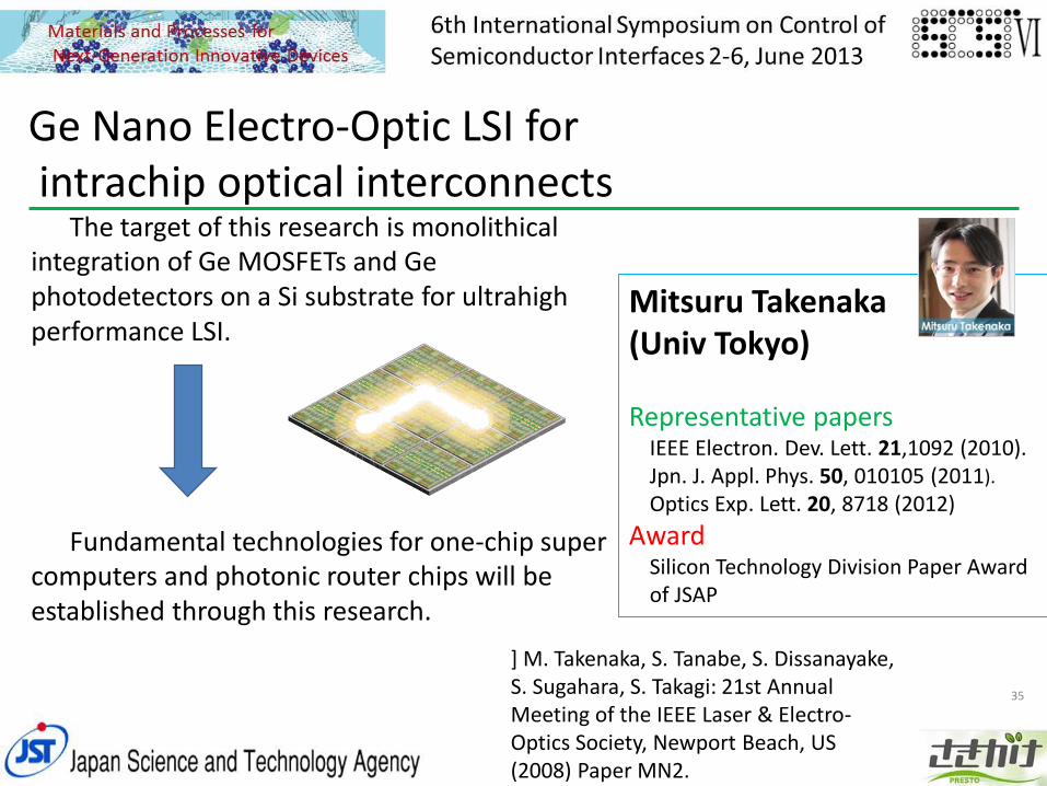
Ge Nano Electro-Optic LSI forintrachip optical interconnects
Mitsuru Takenaka (Univ Tokyo)
Representative papersIEEE Electron. Dev. Lett. 21,1092 (2010).Jpn. J. Appl. Phys. 50, 010105 (2011).
Optics Exp. Lett. 20, 8718 (2012)
AwardSilicon Technology Division Paper Award of JSAP
The target of this research is monolithicalintegration of Ge MOSFETs and Ge photodetectors on a Si substrate for ultrahigh performance LSI.
Fundamental technologies for one-chip super computers and photonic router chips will be established through this research.
35
] M. Takenaka, S. Tanabe, S. Dissanayake, S. Sugahara, S. Takagi: 21st Annual Meeting of the IEEE Laser & Electro-Optics Society, Newport Beach, US (2008) Paper MN2.
0
200
400
600
800
1000
1200
0 1x10¹²
2x10¹²
3x10¹²
4x10¹²
Ele
ctr
on M
ob
ility
(cm
2/V
s)
Ns (cm
-2)
Si electron mobility
Nsub.= 8x1015cm-2
Ge nMOSFETsNsub.= 1x1016cm-2
x1.4
10-11
10-10
10-9
10-8
10-7
10-6
10-5
-4 -3 -2 -1 0 1 2 3
I d a
nd I
s (
A/
m)
Vg (V)
Vd=1V
Vd=50mV
S=176mV/dec
Dit=1.36x10
12cm
2eV
-1
L=70m
~105
Id
Is
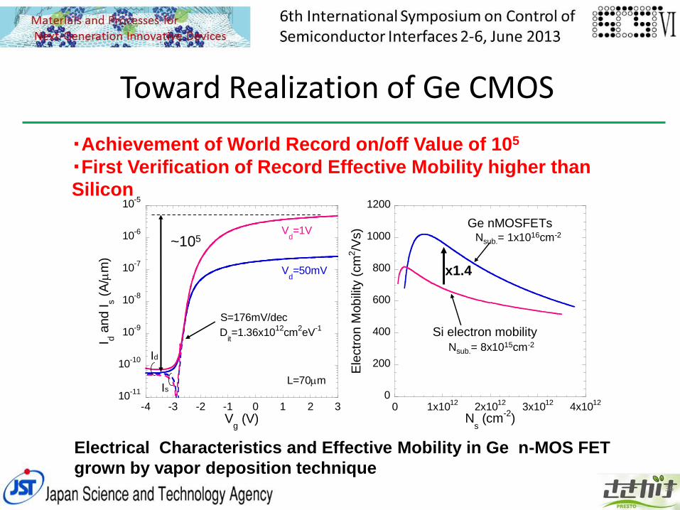
Electrical Characteristics and Effective Mobility in Ge n-MOS FET
grown by vapor deposition technique
Toward Realization of Ge CMOS
・Achievement of World Record on/off Value of 105
・First Verification of Record Effective Mobility higher than
Silicon
36
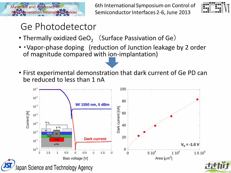
• Thermally oxidized GeO2 (Surface Passivation of Ge)
• ・Vapor-phase doping (reduction of Junction leakage by 2 order of magnitude compared with ion-implantation)
• First experimental demonstration that dark current of Ge PD can be reduced to less than 1 nA
0
20
40
60
80
100
0 5 104
1 105
1.5 105
Dark
curr
ent [n
A]
Area [m2]
Vb = -1.0 V
10-8
10-7
10-6
10-5
10-4
10-3
10-2
10-1
-2-1.5-1-0.500.511.52
Curr
ent [A
]
Bias voltage [V]
Dark current
W/ 1550 nm, 0 dBm
-Vb
Vg
p-Ge
Ni
Al
GeO2
Al2O3
n+Ge
Ge Photodetector
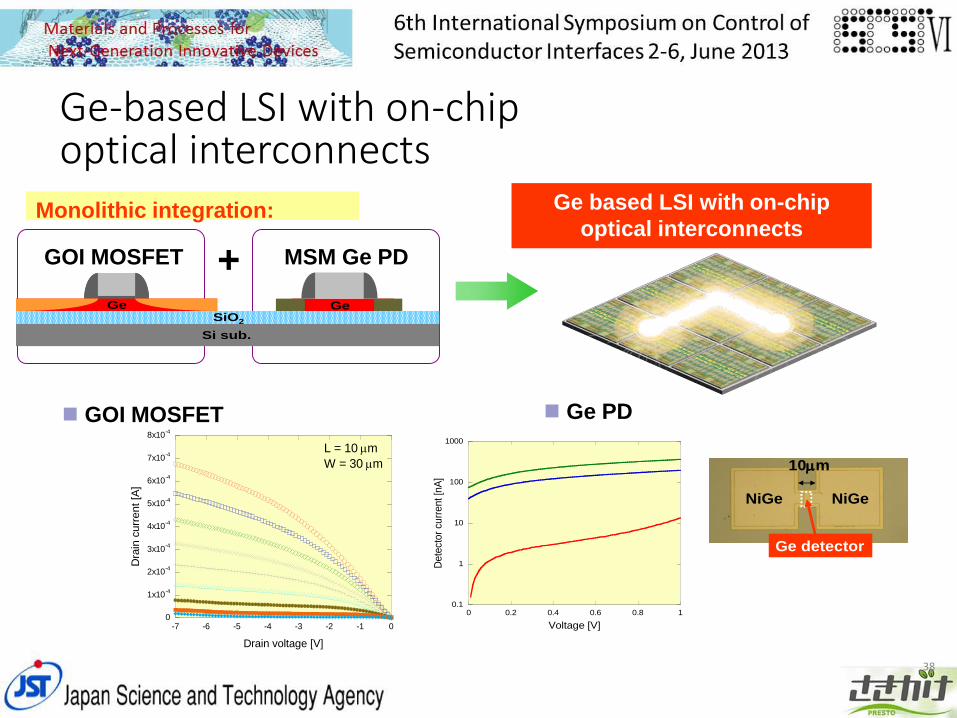
Ge-based LSI with on-chip optical interconnects
0.1
1
10
100
1000
0 0.2 0.4 0.6 0.8 1
Dete
cto
r cu
rrent [n
A]
Voltage [V]
Ge detector
10m
NiGe NiGe
GOI MOSFET +
Monolithic integration:
MSM Ge PD
Si sub.
SiO2
Ge Ge
Ge based LSI with on-chip
optical interconnects
Ge PD GOI MOSFET
0
1x10⁻⁴
2x10⁻⁴
3x10⁻⁴
4x10⁻⁴
5x10⁻⁴
6x10⁻⁴
7x10⁻⁴
8x10⁻⁴
-7 -6 -5 -4 -3 -2 -1 0
Dra
in c
urr
ent
[A]
Drain voltage [V]
L = 10 m
W = 30 m
38
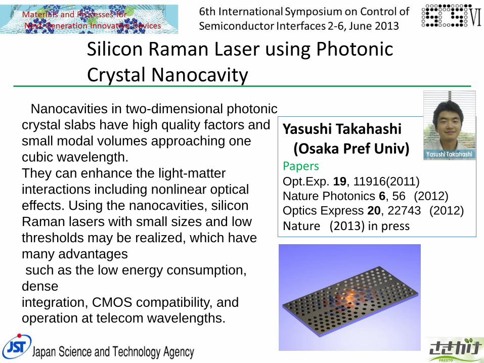
Silicon Raman Laser using Photonic Crystal Nanocavity
Yasushi Takahashi(Osaka Pref Univ)
PapersOpt.Exp. 19, 11916(2011)
Nature Photonics 6, 56 (2012)
Optics Express 20, 22743 (2012)
Nature (2013) in press
Nanocavities in two-dimensional photonic
crystal slabs have high quality factors and
small modal volumes approaching one
cubic wavelength.
They can enhance the light-matter
interactions including nonlinear optical
effects. Using the nanocavities, silicon
Raman lasers with small sizes and low
thresholds may be realized, which have
many advantages
such as the low energy consumption,
dense
integration, CMOS compatibility, and operation at telecom wavelengths.
39
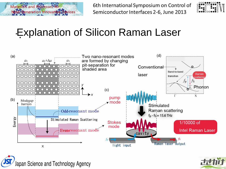
Explanation of Silicon Raman Laser
40
・・
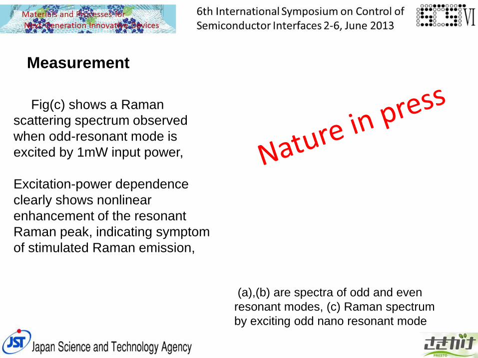
Measurement
(a),(b) are spectra of odd and even
resonant modes, (c) Raman spectrum
by exciting odd nano resonant mode
Fig(c) shows a Raman
scattering spectrum observed
when odd-resonant mode is
excited by 1mW input power,
Excitation-power dependence
clearly shows nonlinear
enhancement of the resonant
Raman peak, indicating symptom
of stimulated Raman emission,
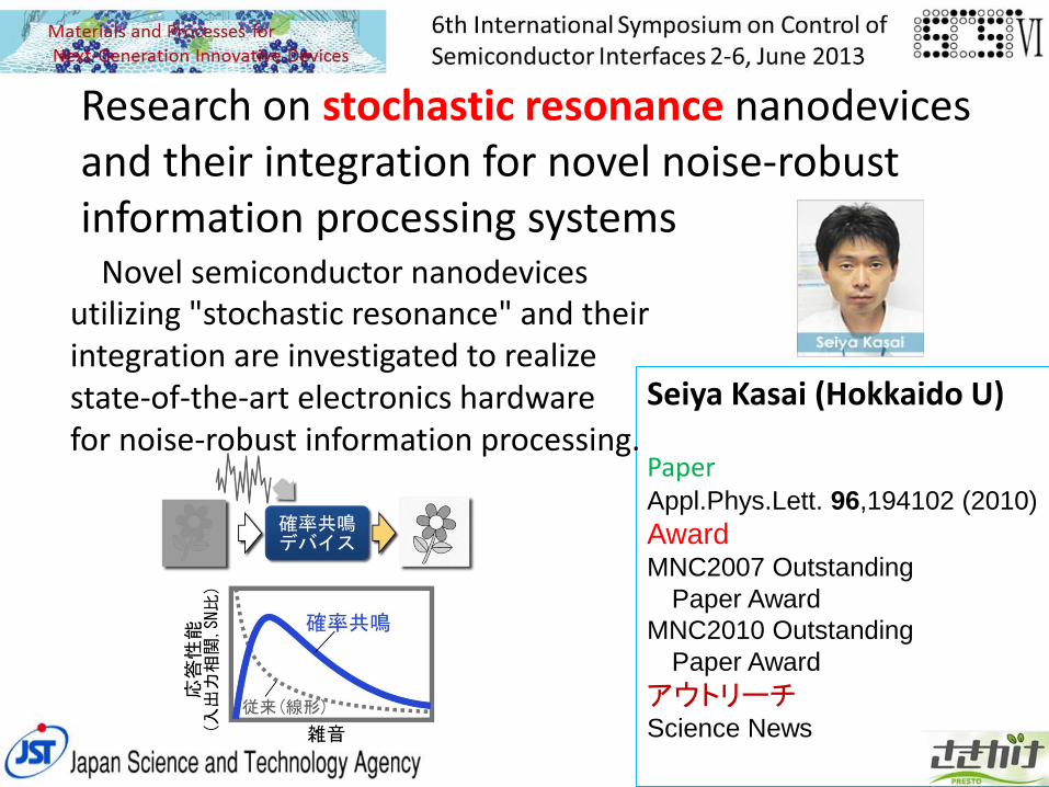
Research on stochastic resonance nanodevicesand their integration for novel noise-robust information processing systems
Seiya Kasai (Hokkaido U)
PaperAppl.Phys.Lett. 96,194102 (2010)
AwardMNC2007 Outstanding
Paper Award
MNC2010 Outstanding
Paper Award
アウトリーチScience News
Novel semiconductor nanodevicesutilizing "stochastic resonance" and their integration are investigated to realize state-of-the-art electronics hardware for noise-robust information processing.
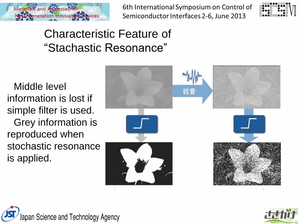
Characteristic Feature of
“Stachastic Resonance”
Middle level
information is lost if
simple filter is used.
Grey information is
reproduced when
stochastic resonance
is applied.
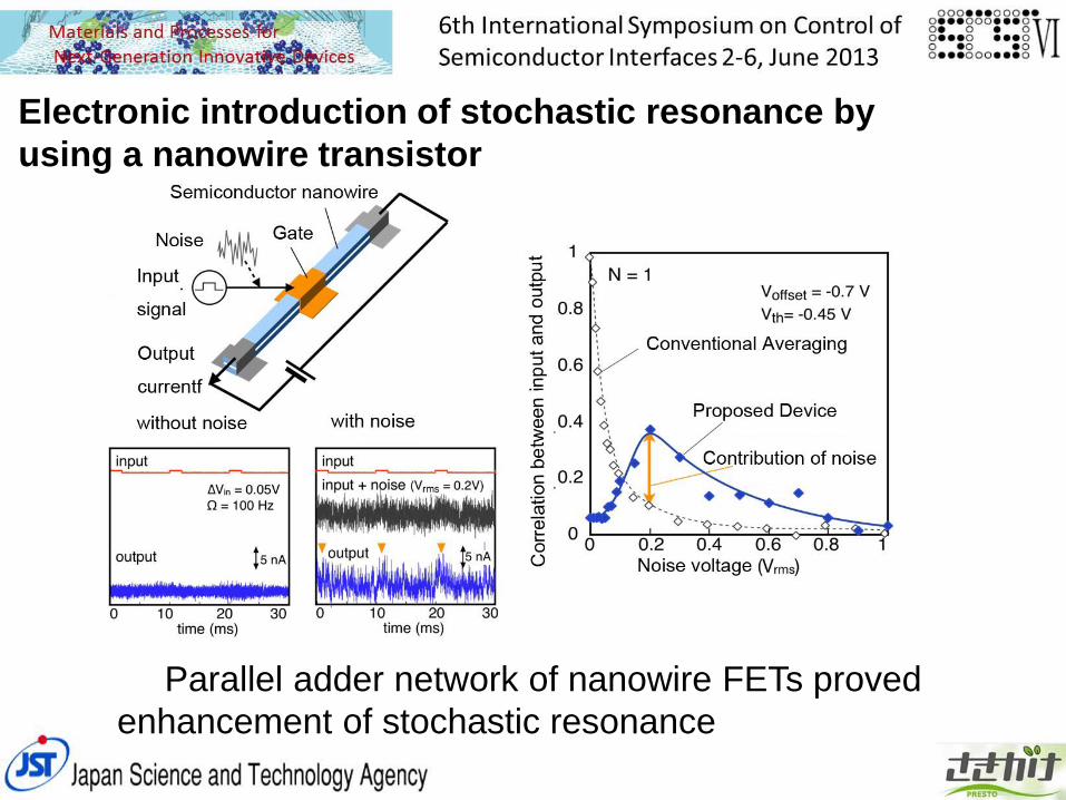
Electronic introduction of stochastic resonance by
using a nanowire transistor
Parallel adder network of nanowire FETs proved
enhancement of stochastic resonance
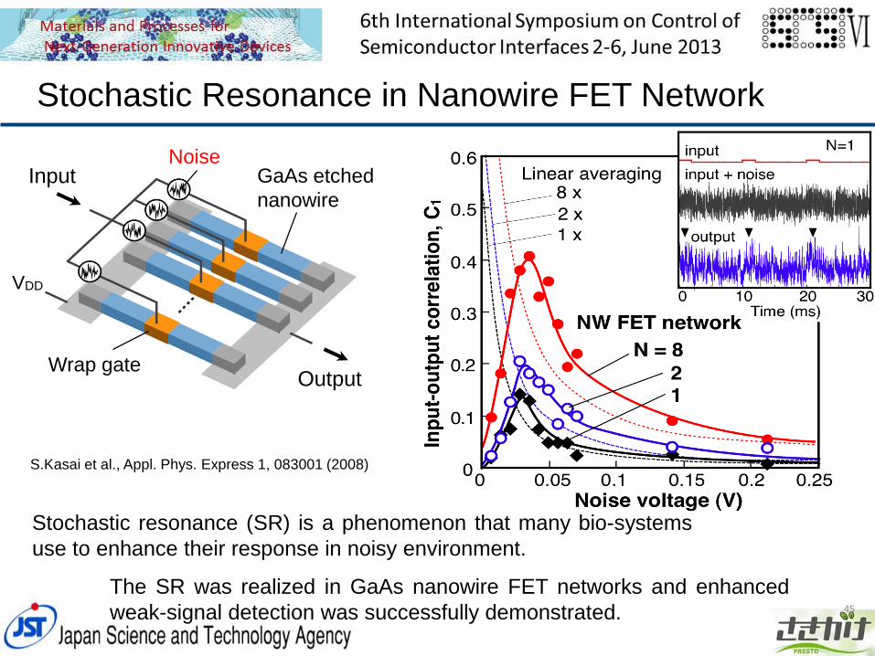
Stochastic Resonance in Nanowire FET Network
GaAs etched
nanowire
Output
Input
VDD
Wrap gate
Noise
Stochastic resonance (SR) is a phenomenon that many bio-systems
use to enhance their response in noisy environment.
The SR was realized in GaAs nanowire FET networks and enhanced
weak-signal detection was successfully demonstrated.
S.Kasai et al., Appl. Phys. Express 1, 083001 (2008)
45
Scatter of
threshold
しきい値のばらつきは入力信号の中心が大きくずれても応答曲線が変わらず、入力信号の変化に追従できる。
先端集積回路の同一設計でのばらつきも利用できる。
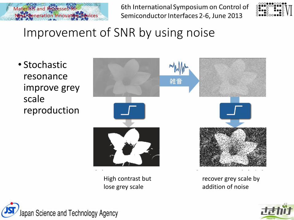
Improvement of SNR by using noise
• Stochastic resonance improve grey scale reproduction
High contrast but lose grey scale
recover grey scale by addition of noise
47
Wide Gap Semiconductors
48
Wide-gap semiconductors
1. N.Mizuochi succeeded in room temperature operation of quantum information processing solid state device and current-induced single photon source by using NV center in diamond p-i-n junction
2. Y.Kangawa succeeded in LPE growth of AlN single crystal for III-N substrate using solid state nitrogen source (LiN)
3. R. Katayama fabricated GaN thin film with periodic modulation of polarity for nonlinear optics
4. M.Higashiwaki succeeded in fabricating Ga2O3 –based device for power electronics
49
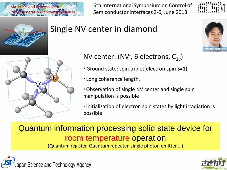
Single NV center in diamond
NV center: (NV-, 6 electrons, C3v)
・Ground state: spin triplet(electron spin S=1)
・Long coherence length.
・Observation of single NV center and single spin manipulation is possible
・Initialization of electron spin states by light irradiation is possible
Quantum information processing solid state device for
room temperature operation(Quantum register, Quantum repeater, single photon emitter …)
50
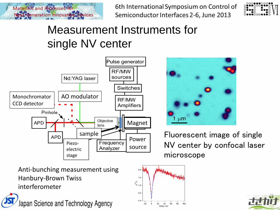
Measurement Instruments for
single NV center
Fluorescent image of single NV center by confocal laser microscope
Anti-bunching measurement using Hanbury-Brown Twissinterferometer
AO modulatorMonochromatorCCD detector
Objective
lens
sample
Piezo-electricstage
Magnet
Power source
51
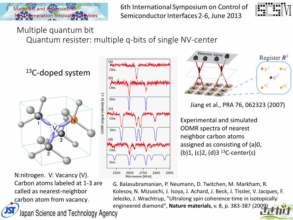
Multiple quantum bitQuantum resister: multiple q-bits of single NV-center
13C-doped system
Experimental and simulated ODMR spectra of nearest neighbor carbon atoms assigned as consisting of (a)0, (b)1, (c)2, (d)3 13C-center(s)
N:nitrogen.V: Vacancy (V).Carbon atoms labeled at 1-3 are called as nearest-neighbor carbon atom from vacancy.
Jiang et al., PRA 76, 062323 (2007)
G. Balasubramanian, P. Neumann, D. Twitchen, M. Markham, R. Kolesov, N. Mizuochi, J. Isoya, J. Achard, J. Beck, J. Tissler, V. Jacques, F. Jelezko, J. Wrachtrup, "Ultralong spin coherence time in isotopically engineered diamond", Nature materials, v. 8, p. 383-387 (2009) 52
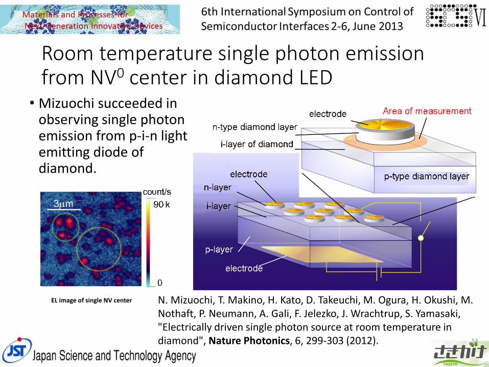
Room temperature single photon emission from NV0 center in diamond LED
• Mizuochi succeeded in observing single photon emission from p-i-n light emitting diode of diamond.
EL image of single NV center N. Mizuochi, T. Makino, H. Kato, D. Takeuchi, M. Ogura, H. Okushi, M. Nothaft, P. Neumann, A. Gali, F. Jelezko, J. Wrachtrup, S. Yamasaki, "Electrically driven single photon source at room temperature in diamond", Nature Photonics, 6, 299-303 (2012). 53
Achievements
Spintronics devices and materials
54
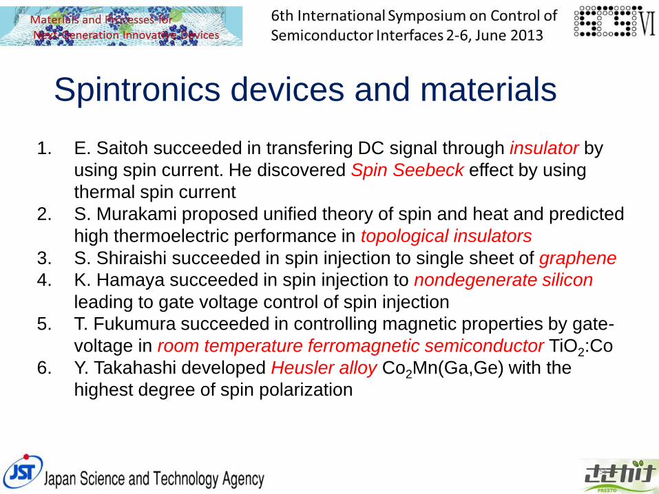
Spintronics devices and materials
1. E. Saitoh succeeded in transfering DC signal through insulator by
using spin current. He discovered Spin Seebeck effect by using
thermal spin current
2. S. Murakami proposed unified theory of spin and heat and predicted
high thermoelectric performance in topological insulators
3. S. Shiraishi succeeded in spin injection to single sheet of graphene
4. K. Hamaya succeeded in spin injection to nondegenerate silicon
leading to gate voltage control of spin injection
5. T. Fukumura succeeded in controlling magnetic properties by gate-
voltage in room temperature ferromagnetic semiconductor TiO2:Co
6. Y. Takahashi developed Heusler alloy Co2Mn(Ga,Ge) with the
highest degree of spin polarization
55
Spintronics based on spin currents and spin-photon coupling in dielectrics
Eiji Saitoh (Tohoku Univ)Representative Papers
Nature 464, 262-266 (2010).Nature materials 9, 894-897 (2010). Nature materials 10, 655 -659 (2011).
AwardsSir Martin Wood PrizeJSPS AwardJapan Academy PrizeJapan IBM Science Prize
PromotionLectureror Keio U→Prof Tohoku U
Special CommentEditor of a Book “Spintronics for Next-Generation Innovative Devices” (John Wiley)
OutreachPress Lecture,JST News
By utilizing the strong interaction between a spin current and an electric field in dielectric materials, the spin-wave spin currents will realize the coherent and low-loss information transmission which can be controlled in terms of light and/or an electric field
Realization of Ultimate Spintronics using pure Spin Current detached from electric current
Spin current is a wave of magnetization in ferromagnet, which is capable of transferring Spin Current (Flow of Spin Angular Moment)
56
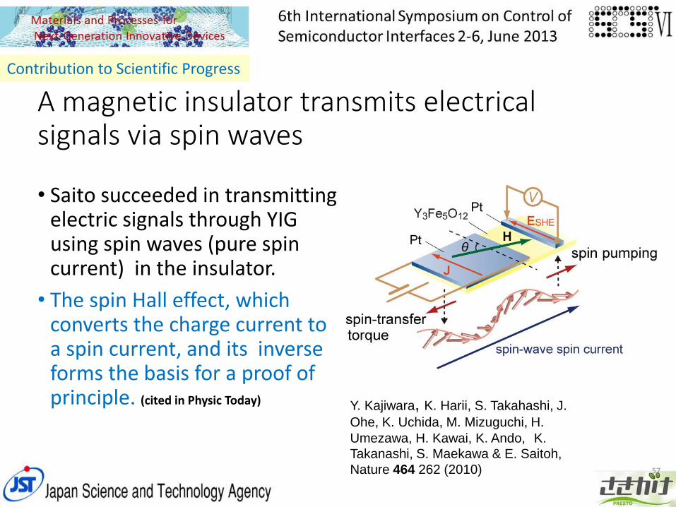
A magnetic insulator transmits electrical signals via spin waves
• Saito succeeded in transmitting electric signals through YIG using spin waves (pure spin current) in the insulator.
• The spin Hall effect, which converts the charge current to a spin current, and its inverse forms the basis for a proof of principle. (cited in Physic Today) Y. Kajiwara, K. Harii, S. Takahashi, J.
Ohe, K. Uchida, M. Mizuguchi, H.
Umezawa, H. Kawai, K. Ando, K.
Takanashi, S. Maekawa & E. Saitoh,
Nature 464 262 (2010) 57
Contribution to Scientific Progress
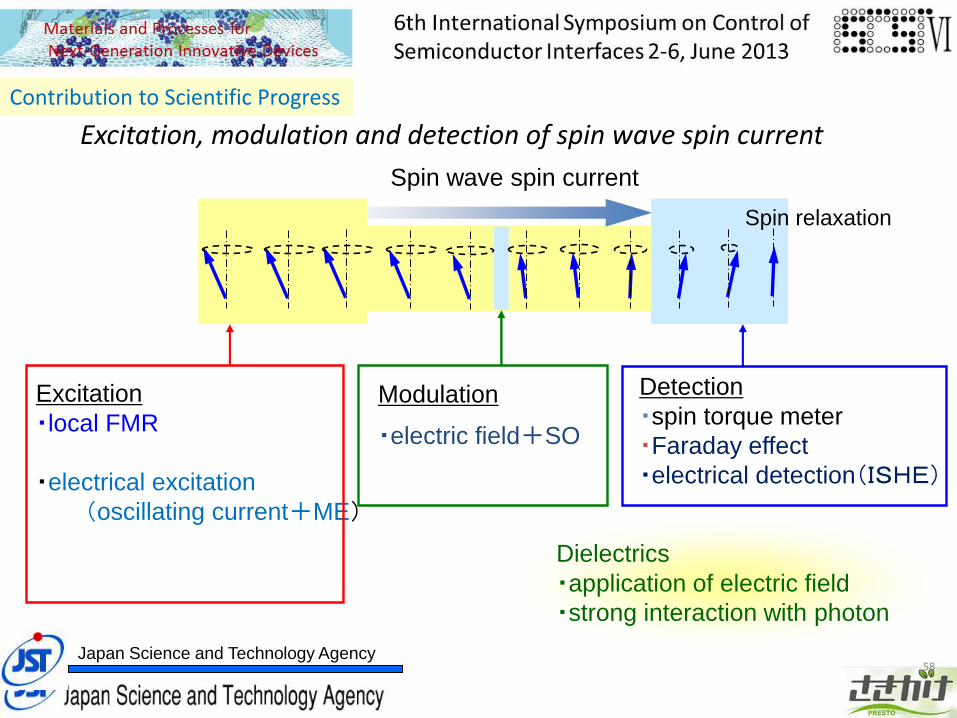
Spin relaxation
Spin wave spin current
Excitation
・local FMR
・electrical excitation
(oscillating current+ME)
Detection
・spin torque meter
・Faraday effect
・electrical detection(ISHE)
Excitation, modulation and detection of spin wave spin current
Dielectrics
・application of electric field
・strong interaction with photon
Modulation
・electric field+SO
Japan Science and Technology Agency58
Contribution to Scientific Progress
59
59
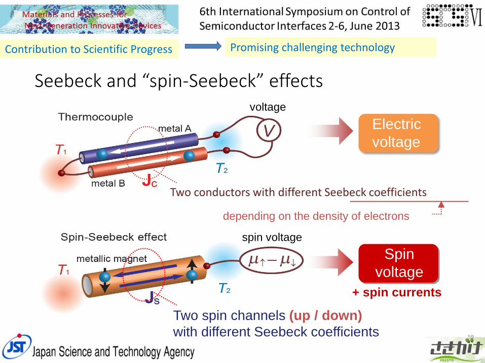
Seebeck and “spin-Seebeck” effects
Spin
voltage
Two spin channels (up / down)
with different Seebeck coefficients
Two conductors with different Seebeck coefficients
depending on the density of electrons
Electric
voltage
+ spin currents
spin voltage
voltage
59
Promising challenging technologyContribution to Scientific Progress
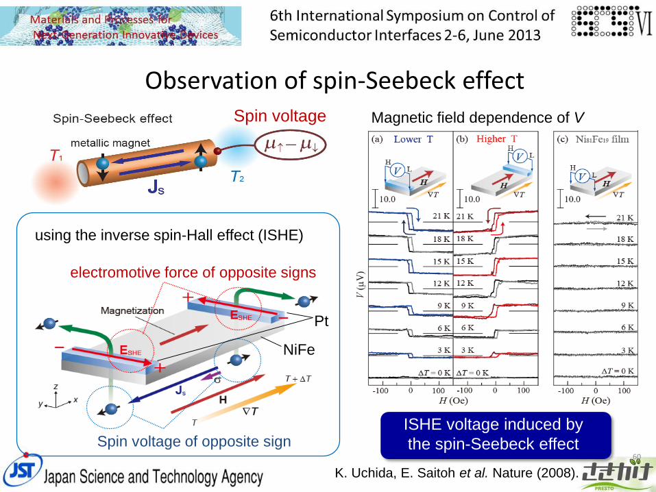
Observation of spin-Seebeck effect
ISHE voltage induced by
the spin-Seebeck effect
Magnetic field dependence of VSpin voltage
electromotive force of opposite signs
Spin voltage of opposite sign
using the inverse spin-Hall effect (ISHE)
K. Uchida, E. Saitoh et al. Nature (2008).
NiFe
Pt
60
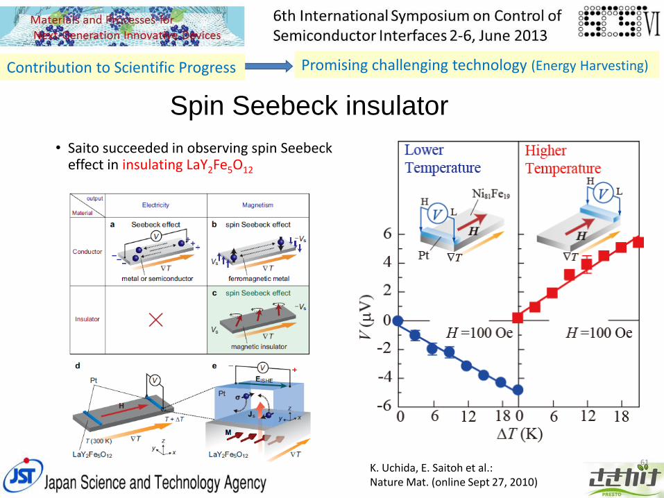
Spin Seebeck insulator
• Saito succeeded in observing spin Seebeckeffect in insulating LaY2Fe5O12
K. Uchida, E. Saitoh et al.:Nature Mat. (online Sept 27, 2010)
61
Promising challenging technology (Energy Harvesting)Contribution to Scientific Progress
3) Quantum spin Hall systems as candidates for efficient thermoelectrics
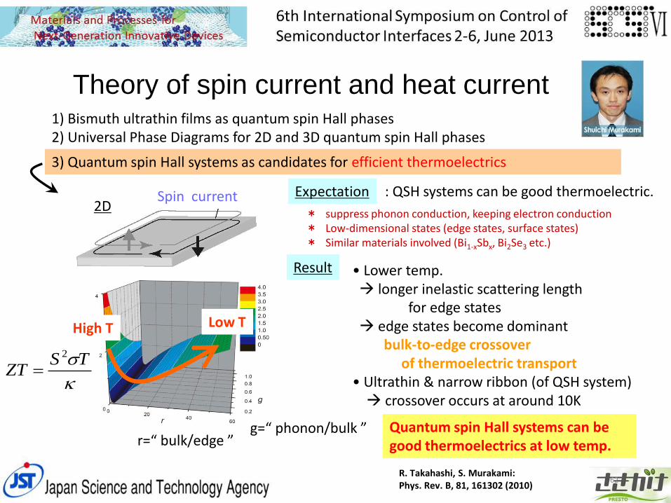
Theory of spin current and heat current
* suppress phonon conduction, keeping electron conduction* Low-dimensional states (edge states, surface states)* Similar materials involved (Bi1-xSbx, Bi2Se3 etc.)
2DSpin current
Quantum spin Hall systems can be good thermoelectrics at low temp.
1) Bismuth ultrathin films as quantum spin Hall phases 2) Universal Phase Diagrams for 2D and 3D quantum spin Hall phases
Low THigh T
TSZT
2
r=“ bulk/edge ”g=“ phonon/bulk ”
• Lower temp. longer inelastic scattering length
for edge states edge states become dominant
bulk-to-edge crossover of thermoelectric transport
• Ultrathin & narrow ribbon (of QSH system) crossover occurs at around 10K
Result
Expectation : QSH systems can be good thermoelectric.
R. Takahashi, S. Murakami: Phys. Rev. B, 81, 161302 (2010)
62
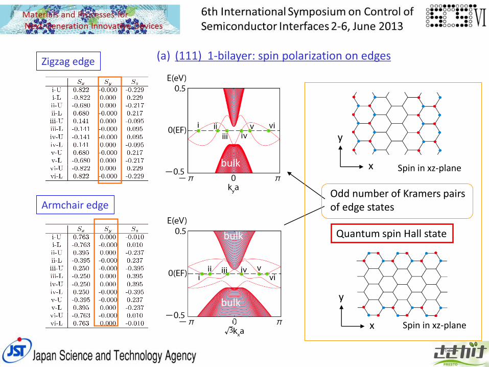
Quantum spin Hall state
Odd number of Kramers pairsof edge states
bulk
bulk
bulk
bulk
Zigzag edge
Armchair edge
x
y
Spin in xz-plane
x
y
bulk
(a) (111) 1-bilayer: spin polarization on edges
Spin in xz-plane
63
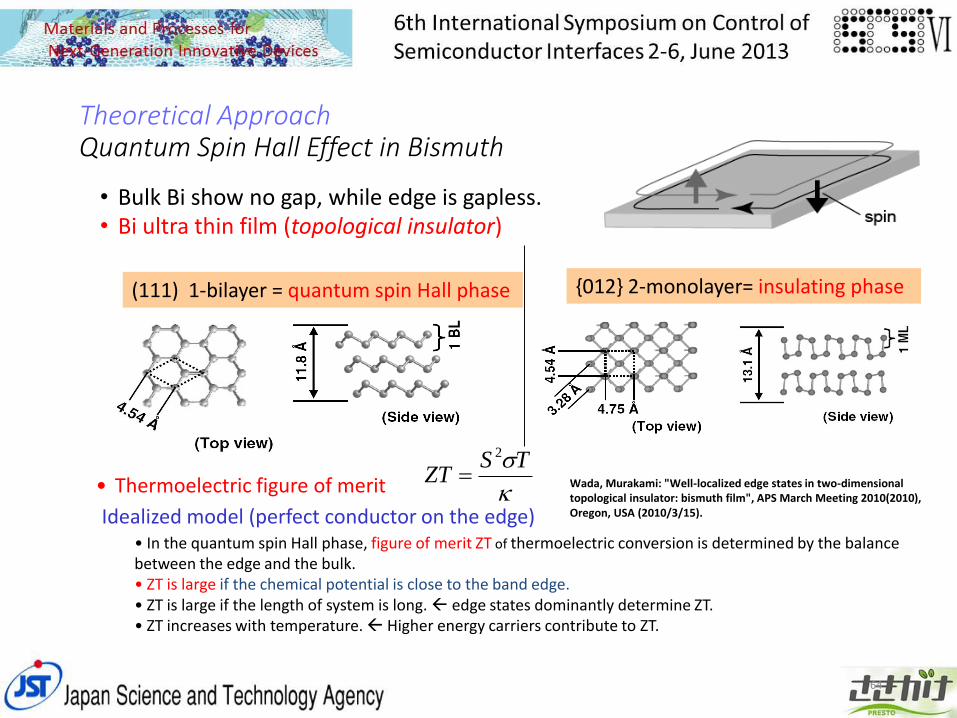
{012} 2-monolayer= insulating phase (111) 1-bilayer = quantum spin Hall phase
• Thermoelectric figure of merit
• In the quantum spin Hall phase, figure of merit ZT of thermoelectric conversion is determined by the balance between the edge and the bulk. • ZT is large if the chemical potential is close to the band edge.• ZT is large if the length of system is long. edge states dominantly determine ZT.• ZT increases with temperature. Higher energy carriers contribute to ZT.
Idealized model (perfect conductor on the edge)
Theoretical ApproachQuantum Spin Hall Effect in Bismuth
• Bulk Bi show no gap, while edge is gapless.• Bi ultra thin film (topological insulator)
TSZT
2
Wada, Murakami: "Well-localized edge states in two-dimensional topological insulator: bismuth film", APS March Meeting 2010(2010), Oregon, USA (2010/3/15).
64
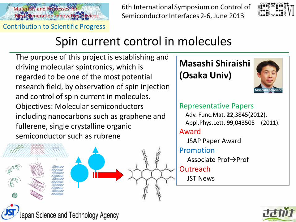
Spin current control in molecules
Masashi Shiraishi(Osaka Univ)
Representative PapersAdv. Func.Mat. 22,3845(2012).Appl.Phys.Lett. 99,043505 (2011).
AwardJSAP Paper Award
PromotionAssociate Prof→Prof
OutreachJST News
The purpose of this project is establishing and driving molecular spintronics, which is regarded to be one of the most potential research field, by observation of spin injection and control of spin current in molecules.Objectives: Molecular semiconductors including nanocarbons such as graphene and fullerene, single crystalline organic semiconductor such as rubrene
65
Contribution to Scientific Progress
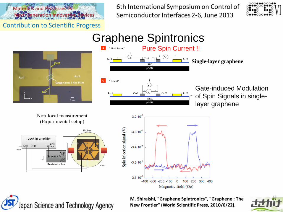
Graphene Spintronics
Gate-induced Modulation
of Spin Signals in single-
layer graphene
Pure Spin Current !!
M. Shiraishi, "Graphene Spintronics", "Graphene : The New Frontier" (World Scientific Press, 2010/6/22).
Single-layer graphene
66
Contribution to Scientific Progress
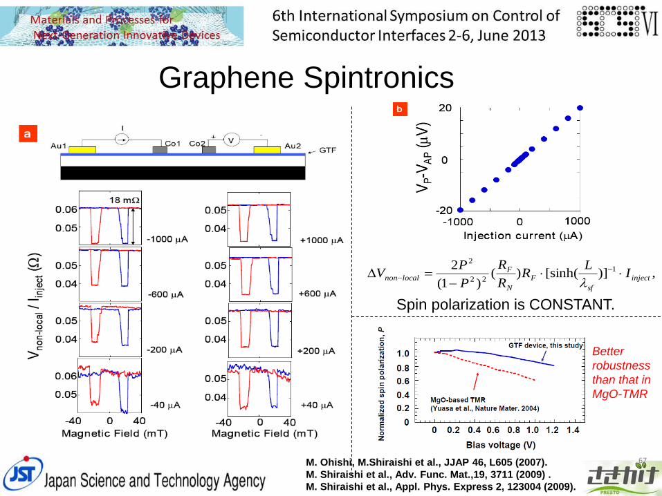
Graphene Spintronics
,)][sinh()()1(
2 1
22
2
inject
sf
F
N
Flocalnon I
LR
R
R
P
PV
M. Ohishi, M.Shiraishi et al., JJAP 46, L605 (2007).
M. Shiraishi et al., Adv. Func. Mat.,19, 3711 (2009) .
M. Shiraishi et al., Appl. Phys. Express 2, 123004 (2009).
Spin polarization is CONSTANT.
Better
robustness
than that in
MgO-TMR
67
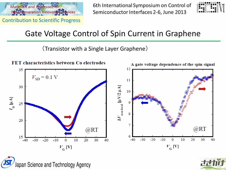
Gate Voltage Control of Spin Current in Graphene
(Transistor with a Single Layer Graphene)
68
Contribution to Scientific Progress
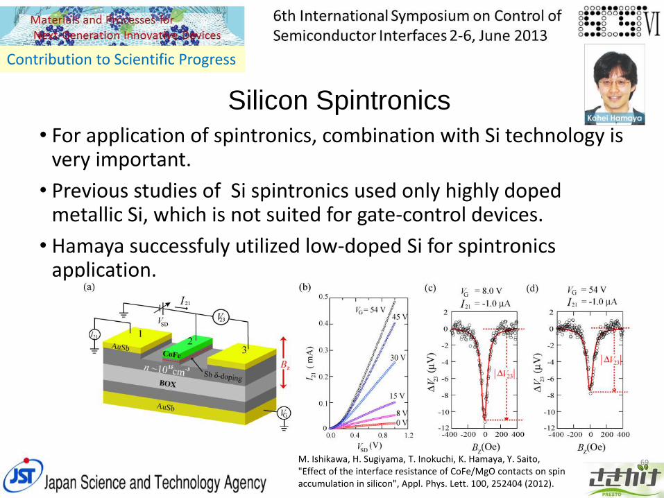
Silicon Spintronics
• For application of spintronics, combination with Si technology is very important.
• Previous studies of Si spintronics used only highly doped metallic Si, which is not suited for gate-control devices.
• Hamaya successfuly utilized low-doped Si for spintronics application.
M. Ishikawa, H. Sugiyama, T. Inokuchi, K. Hamaya, Y. Saito, "Effect of the interface resistance of CoFe/MgO contacts on spin accumulation in silicon", Appl. Phys. Lett. 100, 252404 (2012).
69
Contribution to Scientific Progress
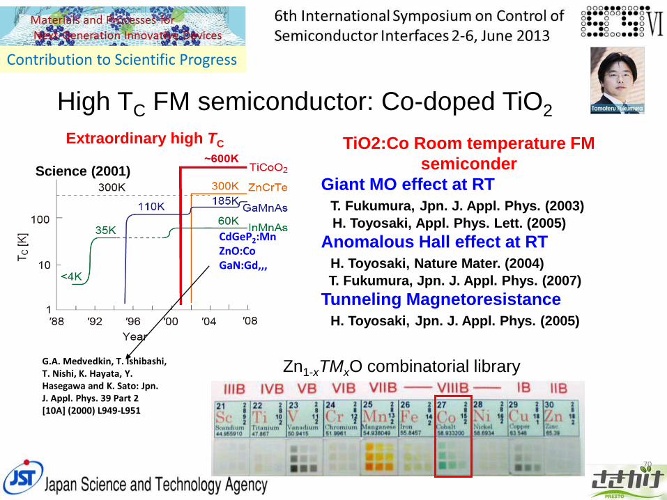
High TC FM semiconductor: Co-doped TiO2
Science (2001)
Extraordinary high TC TiO2:Co Room temperature FM
semiconder
Giant MO effect at RT
T. Fukumura, Jpn. J. Appl. Phys. (2003)
H. Toyosaki, Appl. Phys. Lett. (2005)
Anomalous Hall effect at RT
H. Toyosaki, Nature Mater. (2004)
T. Fukumura, Jpn. J. Appl. Phys. (2007)
Tunneling Magnetoresistance
H. Toyosaki, Jpn. J. Appl. Phys. (2005)
CdGeP2:MnZnO:CoGaN:Gd,,,
Zn1-xTMxO combinatorial libraryG.A. Medvedkin, T. Ishibashi, T. Nishi, K. Hayata, Y. Hasegawa and K. Sato: Jpn. J. Appl. Phys. 39 Part 2 [10A] (2000) L949-L951
70
Contribution to Scientific Progress
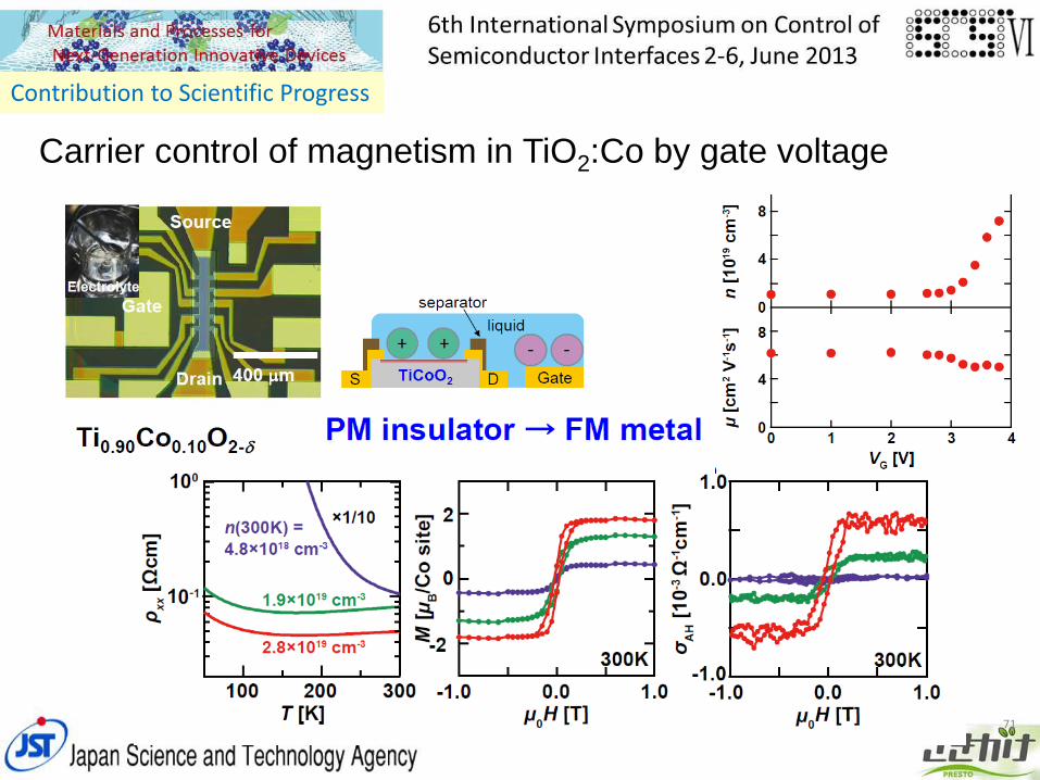
Carrier control of magnetism in TiO2:Co by gate voltage
71
Contribution to Scientific Progress
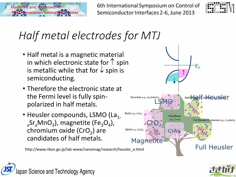
Half metal electrodes for MTJ
EF
http://www.riken.go.jp/lab-www/nanomag/research/heusler_e.html
• Half metal is a magnetic material in which electronic state for spin is metallic while that for spin is semiconducting.
• Therefore the electronic state at the Fermi level is fully spin-polarized in half metals.
• Heusler compounds, LSMO (La1-
xSrxMnO3), magnetite (Fe3O4), chromium oxide (CrO2) are candidates of half metals.
LSMOHalf Heusler
Full HeuslerMagnetite
CrO2
CrAs
72
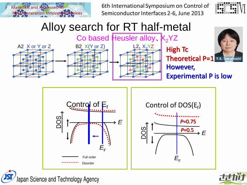
Control of Ef
P=0.5
P=0.75
Control of DOS(Ef)
L21 X2YZB2 X(Y or Z)A2 X or Y or Z High TcTheoretical P=1However,Experimental P is low
Co based Heusler alloy、X2YZ
Alloy search for RT half-metal
Full order
Disorder
73
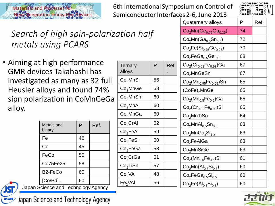
Search of high spin-polarization half metals using PCARS
• Aiming at high performance GMR devices Takahashi has investigated as many as 32 full Heusler alloys and found 74% sipn polarization in CoMnGeGaalloy.
Ternary
alloys
P Ref
.
Co2MnSi 56
Co2MnGe 58
Co2MnSn 60
Co2MnAl 60
Co2MnGa 60
Co2CrAl 62
Co2FeAl 59
Co2FeSi 60
Co2FeGa 58
Co2CrGa 61
Co2TiSn 57
Co2VAl 48
Fe2VAl 56
Quaternary alloys P Ref.
Co2Mn(Ge0.75Ga0.25) 74
Co2Mn(Ga0.5Sn0.5) 72
Co2Fe(Si0.75Ge0.25) 70
Co2FeGa0.5Ge0.5 68
Co2(Cr0.02Fe0.98)Ga 67
Co2MnGeSn 67
Co2(Mn0.95Fe0.05)Sn 65
(CoFe)2MnGe 65
Co2(Mn0.5Fe0.5)Ga 65
Co2(Cr0.02Fe0.98)Si 65
Co2MnTiSn 64
Co2MnAl0.5Sn0.5 63
Co2MnGaxSi1-x 63
Co2FeAlGa 63
Co2MnSiGe 63
Co2(Mn0.5Fe0.5)Si 61
Co2Mn(Al0.5Si0.5) 60
Co2FeGa0.5Si0.5 60
Co2Fe(Al0.5Si0.5) 60
Metals and
binaryP Ref.
Fe 46
Co 45
FeCo 50
Co75Fe25 58
B2-FeCo 60
[Co/Pd]n 60
Japan Science and Technology Agency74
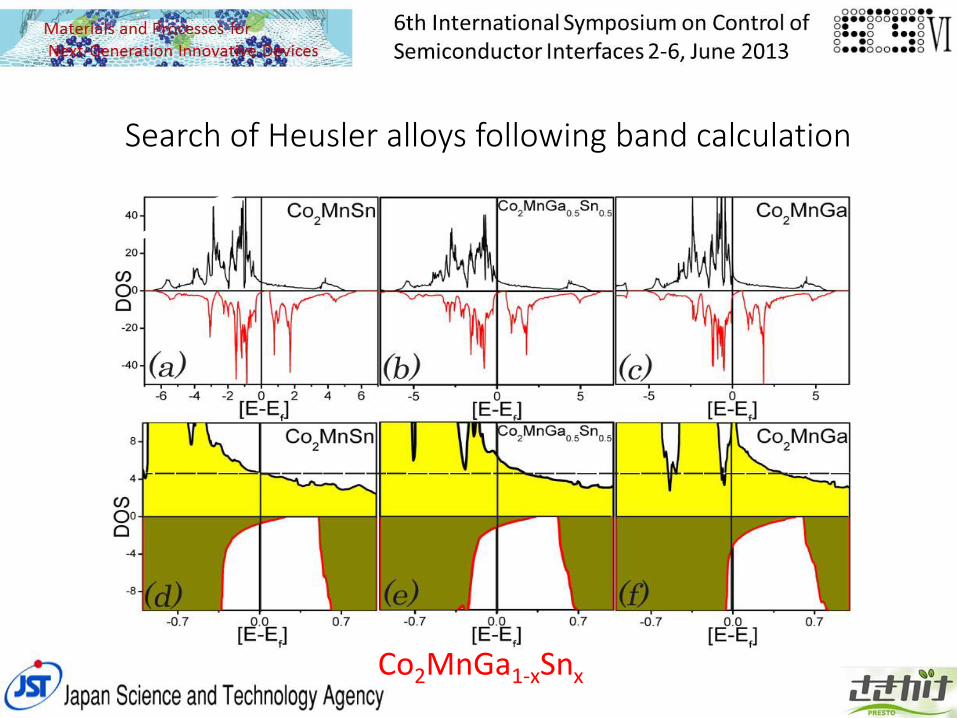
Search of Heusler alloys following band calculation
Co2MnGa1-xSnx
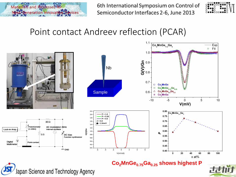
Point contact Andreev reflection (PCAR)
V
Lock-in Amp.
Digital
MultimeterPoint-contact
Potentiometer
(1-100)
1
30
AC modulation 2kHzinternal oscillator
DC biasFunction synthesizer
GND
V
Lock-in Amp.
Digital
MultimeterPoint-contact
Potentiometer
(1-100)
1
30
AC modulation 2kHzinternal oscillator
DC biasFunction synthesizer
GND -6 -4 -2 0 2 4 6
0.0
0.2
0.4
0.6
0.8
1.0
1.2
1.4
1.6
1.8
2.0
2.2
P = 1.0
P = 0.35
P = 0.0
Z = 0.0
= 1.5meV
V(mVolt)
G(V
)/G
n
Nb
Sample
Co2MnGe0.75Ga0.25 shows highest P
Light-Induced ultrafast magnetization reversal
• The response time of magnetization reversal is usually limited by the spin dynamics which follow Landau-Lifshitz-Gilbert equation.
• By a collaboration of Nihon Univ. group and Radbout Univ. group, ultrafast magnetization switching (less than ps) was accomplished in the vicinity of the compensation point of MO-recording media.
77
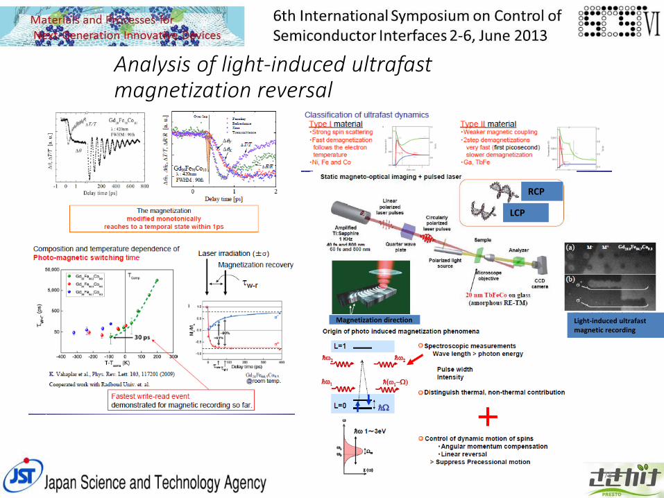
Analysis of light-induced ultrafast magnetization reversal
Tsukamoto (Nihon U.)
RCP
LCP
Magnetization direction Light-induced ultrafast magnetic recording
78
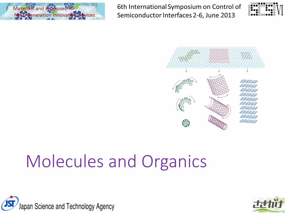
Molecules and Organics
79
1. K. Machda fabricated nano structured graphene to find single electron and quantum effect
2. H. Yamamoto fabricated organic FET with high field effect mobility using voltage controlled Mott-transition. He also succeeded in electrical control of superconductivity in organic material
3. S. Noda succeeded in growing single graphene sheet on insulating substrate by metal-free process
4. J. Nishinaga succeeded in delta-doping of C60 in GaAs thin film during MBE growth
Molecules and Organics
80
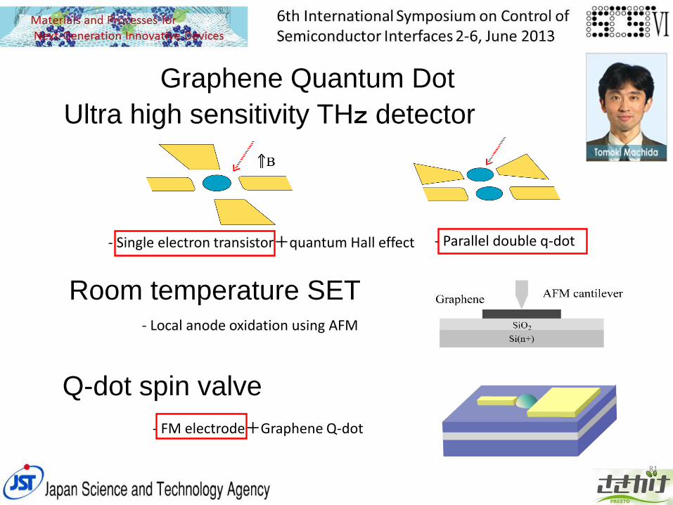
Graphene Quantum Dot
Ultra high sensitivity THz detector
Room temperature SET
Q-dot spin valve
- Parallel double q-dot- Single electron transistor+quantum Hall effect
- Local anode oxidation using AFM
- FM electrode+Graphene Q-dot
81
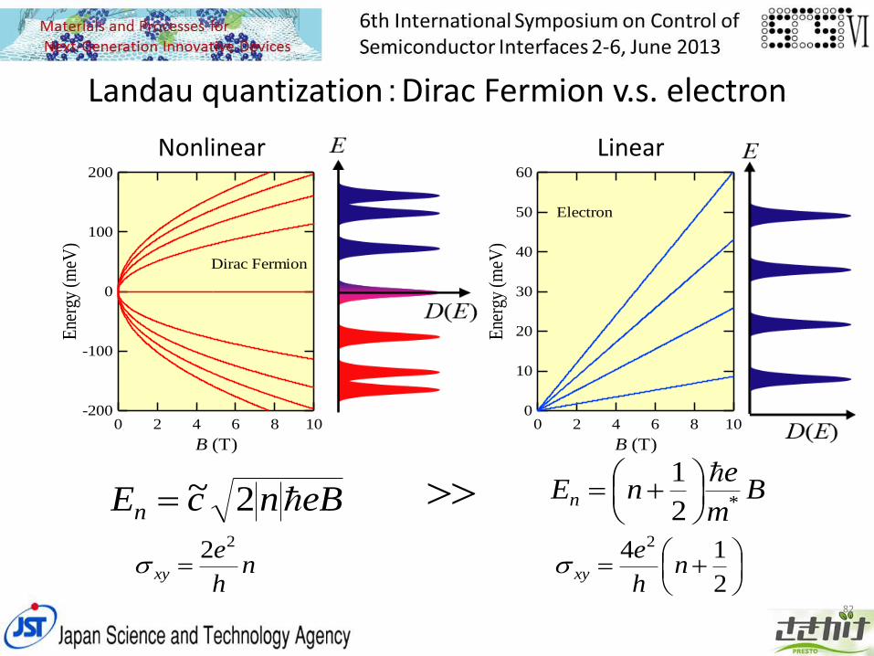
Landau quantization:Dirac Fermion v.s. electron
eBncEn 2~ Bm
enEn *2
1
nh
exy
22
2
14 2
nh
exy
-200
-100
0
100
200
Ene
rgy
(meV
)
1086420
B (T)
Dirac Fermion
60
50
40
30
20
10
0
Ene
rgy
(meV
)
1086420
B (T)
Electron
LinearNonlinear
82
83
Graphene single QD
83
500 nm
83
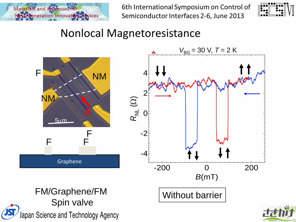
Nonlocal Magnetoresistance
B5m
NM
F NM
F
VBG = 30 V, T = 2 K
4
2
0
-2
-4
RN
L (
)
-200 0 200
B(mT)
Graphene
F F
FM/Graphene/FM
Spin valveWithout barrier
84
Development of novel organic devices based on electronic correlation
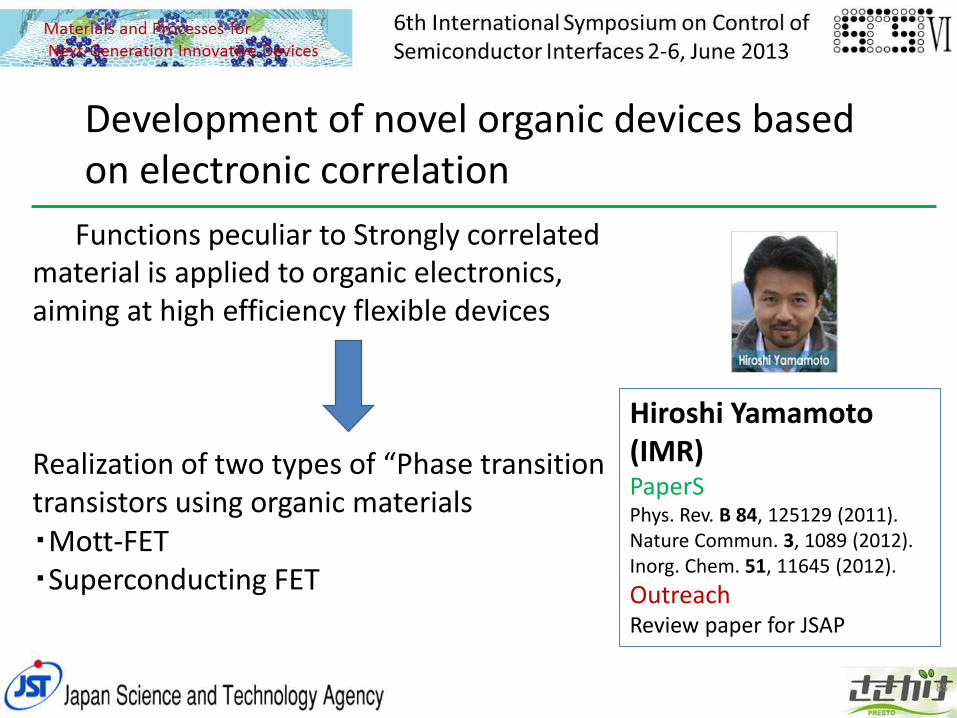
Hiroshi Yamamoto(IMR)PaperSPhys. Rev. B 84, 125129 (2011).Nature Commun. 3, 1089 (2012).Inorg. Chem. 51, 11645 (2012).
OutreachReview paper for JSAP
Functions peculiar to Strongly correlated material is applied to organic electronics, aiming at high efficiency flexible devices
Realization of two types of “Phase transition transistors using organic materials・Mott-FET・Superconducting FET
85
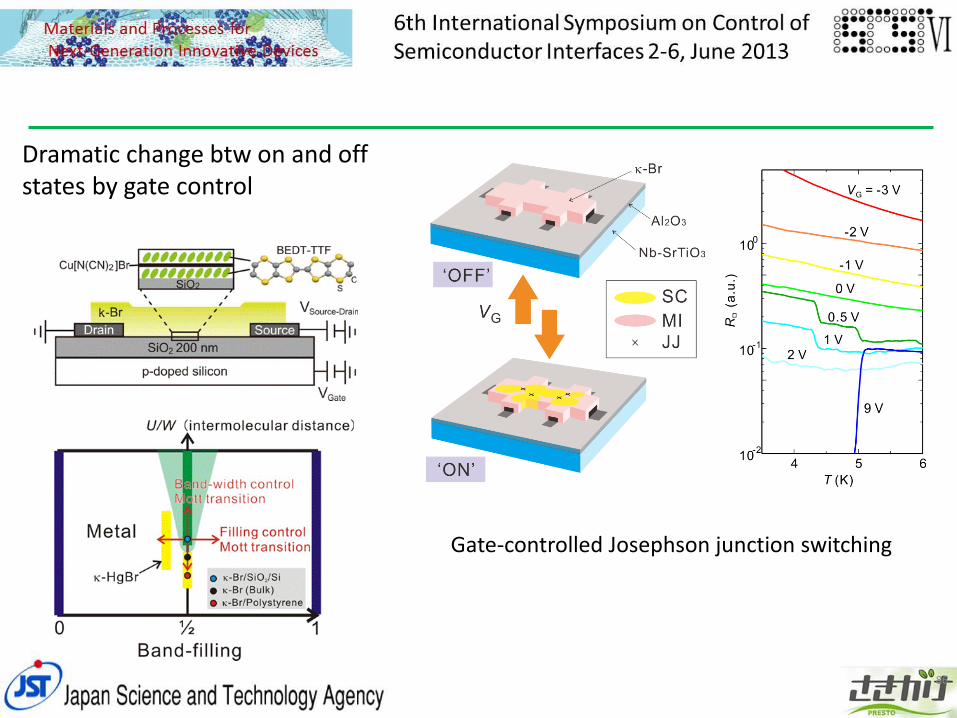
Dramatic change btw on and off states by gate control
Gate-controlled Josephson junction switching
86
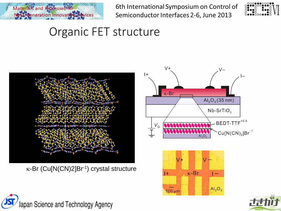
-Br (Cu[N(CN)2]Br-1) crystal structure
Organic FET structure
87
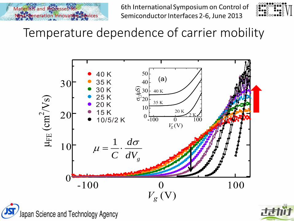
Temperature dependence of carrier mobility
gdV
d
C
1
88
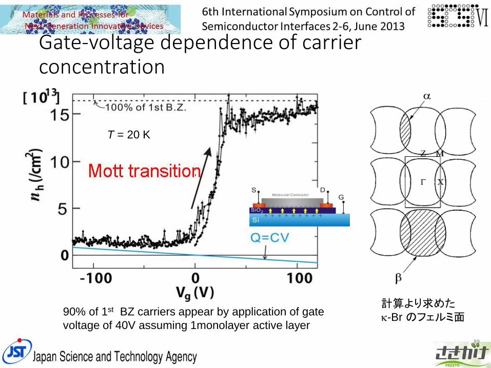
Gate-voltage dependence of carrier concentration
計算より求めた-Br のフェルミ面90% of 1st BZ carriers appear by application of gate
voltage of 40V assuming 1monolayer active layer
T = 20 K
89
Outcomes(1) Contribution to Scientific Progress, (2) Development to Practical Application, (3) Results for future innovation, (4) Promising challenging technology, (5) Nurture of future scientific leader
Products of the Research Project
90
(1) Contribution to Scientific Progress
• Eiji Saitoh: Establishment of Concept of Spin Current in Insulator, Discovery of Spin Seebek Effect
• Masashi Shiraishi: First Verification of Injection of Pure Spin Current into Graphene, and Graphene-based GMR Device
• Tomoteru Fukumura: Realization of Voltage-Controlled Magnetization Change in TiO2:Co Room-Temperature Ferromagnetic Semiconductor
• Kohei Hamaya: Establishment of Spin Injection to Nondegenerate Semiconductor Silicon
アウトカム
91
(2) Development for Practical Application
• Mitsuru Takenaka:Monolithic Integration of Ge-Channel High Performance MOS Transistor and Ge-Photodetector
• Katsuhiro Tomioka:World Record SS-value of 21mV/dec in Tunnel FET using InAs Nanowires on Si
• Akira Tsukamoto: Elucidation of Ultra-High Speed Light-Induced Magnetization Reversal Mechanism for Next-Generation Magnetic Recording
• Tomoki Machida: High Sensitivity THz Detector Using Graphene Quantum Dot
アウトカム
92
(3) Results for future innovation
• Norikazu Mizuochi:Single photon source for quantum information communication which can be operated at Room Temperature using NV center in Diamond LED
• Yasushi Takahashi: Realization of silicon Raman laser using extremely high Q value of photonic crystal
• Suguru Noda: Direct growth of metal-free graphene on quartz using novel etching deposition technique.
アウトカム
93
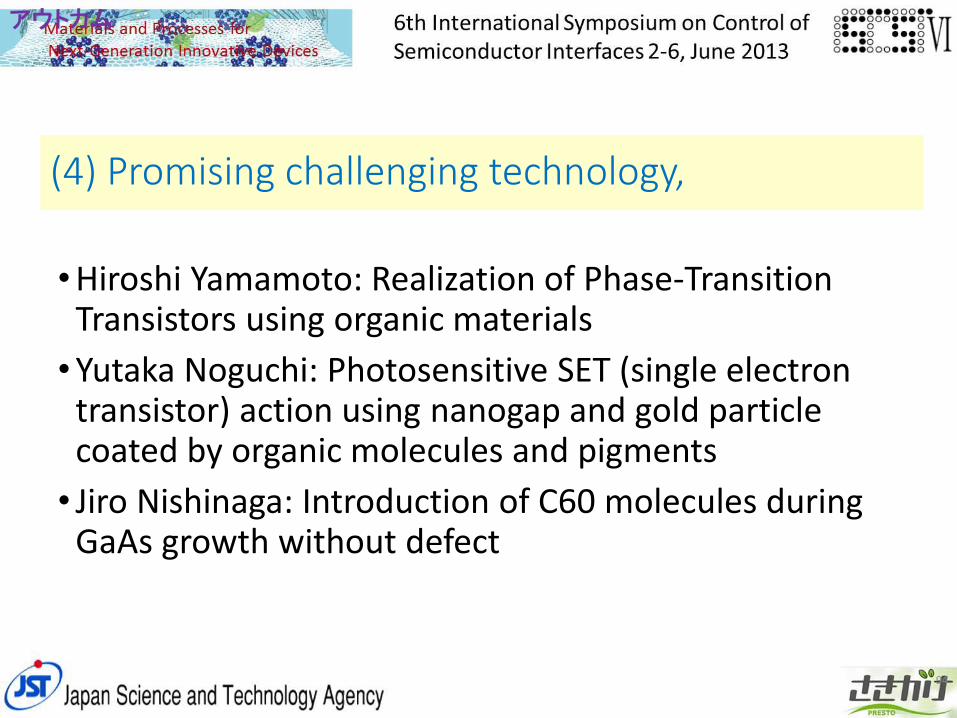
(4) Promising challenging technology,
• Hiroshi Yamamoto: Realization of Phase-Transition Transistors using organic materials
• Yutaka Noguchi: Photosensitive SET (single electron transistor) action using nanogap and gold particle coated by organic molecules and pigments
• Jiro Nishinaga: Introduction of C60 molecules during GaAs growth without defect
アウトカム
94
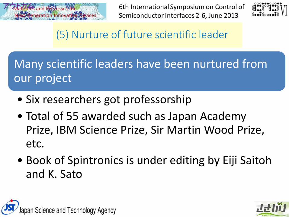
(5) Nurture of future scientific leader
Many scientific leaders have been nurtured from our project
• Six researchers got professorship
• Total of 55 awarded such as Japan Academy Prize, IBM Science Prize, Sir Martin Wood Prize, etc.
• Book of Spintronics is under editing by Eiji Saitohand K. Sato
アウトカム
95
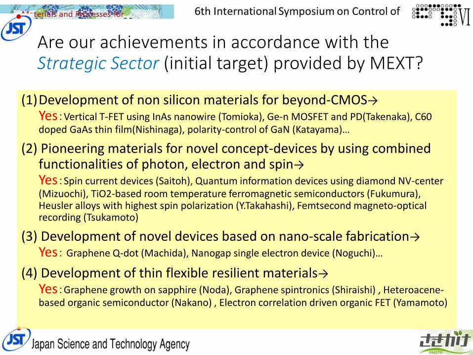
Are our achievements in accordance with the Strategic Sector (initial target) provided by MEXT?
(1)Development of non silicon materials for beyond-CMOS→
Yes:Vertical T-FET using InAs nanowire (Tomioka), Ge-n MOSFET and PD(Takenaka), C60doped GaAs thin film(Nishinaga), polarity-control of GaN (Katayama)…
(2) Pioneering materials for novel concept-devices by using combined functionalities of photon, electron and spin→
Yes:Spin current devices (Saitoh), Quantum information devices using diamond NV-center (Mizuochi), TiO2-based room temperature ferromagnetic semiconductors (Fukumura), Heusler alloys with highest spin polarization (Y.Takahashi), Femtsecond magneto-optical recording (Tsukamoto)
(3) Development of novel devices based on nano-scale fabrication→
Yes: Graphene Q-dot (Machida), Nanogap single electron device (Noguchi)…
(4) Development of thin flexible resilient materials→
Yes:Graphene growth on sapphire (Noda), Graphene spintronics (Shiraishi) , Heteroacene-based organic semiconductor (Nakano) , Electron correlation driven organic FET (Yamamoto)
96
How the Project MANAGED?
JST SATO-PRESTO PROJECT
Materials and Processes for Next-Generation Innovative Devices
97
Duration and Budgets
• Duration: 3.5 years
• Budget: 40MYen (~400KEuros) per person
• Members: 33 (Total 1.4BYen~14MEuro)
• Average age at adoption: 34.5 years old
• Affiliation: Universities: 25, Government Agencies: 8
For Comparison: Case of Watanabe-CRESTDuration Max 5.5 years
Budget 150-500 M Yen (1.5-5 M Euro) per teamTeams: 18
98
99
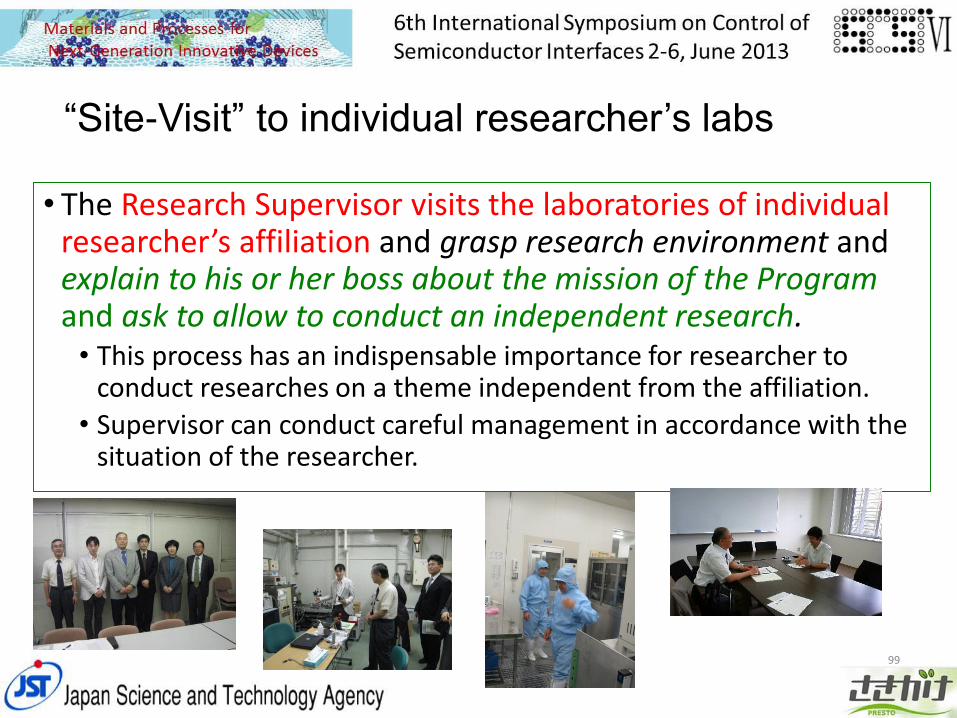
“Site-Visit” to individual researcher’s labs
• The Research Supervisor visits the laboratories of individual researcher’s affiliation and grasp research environment and explain to his or her boss about the mission of the Program and ask to allow to conduct an independent research.
• This process has an indispensable importance for researcher to conduct researches on a theme independent from the affiliation.
• Supervisor can conduct careful management in accordance with the situation of the researcher.
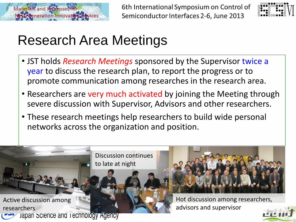
Research Area Meetings
• JST holds Research Meetings sponsored by the Supervisor twice a year to discuss the research plan, to report the progress or to promote communication among researches in the research area.
• Researchers are very much activated by joining the Meeting through severe discussion with Supervisor, Advisors and other researchers.
• These research meetings help researchers to build wide personal networks across the organization and position.
Active discussion among researchers
Discussion continuesto late at night
Hot discussion among researchers, advisors and supervisor
100
101
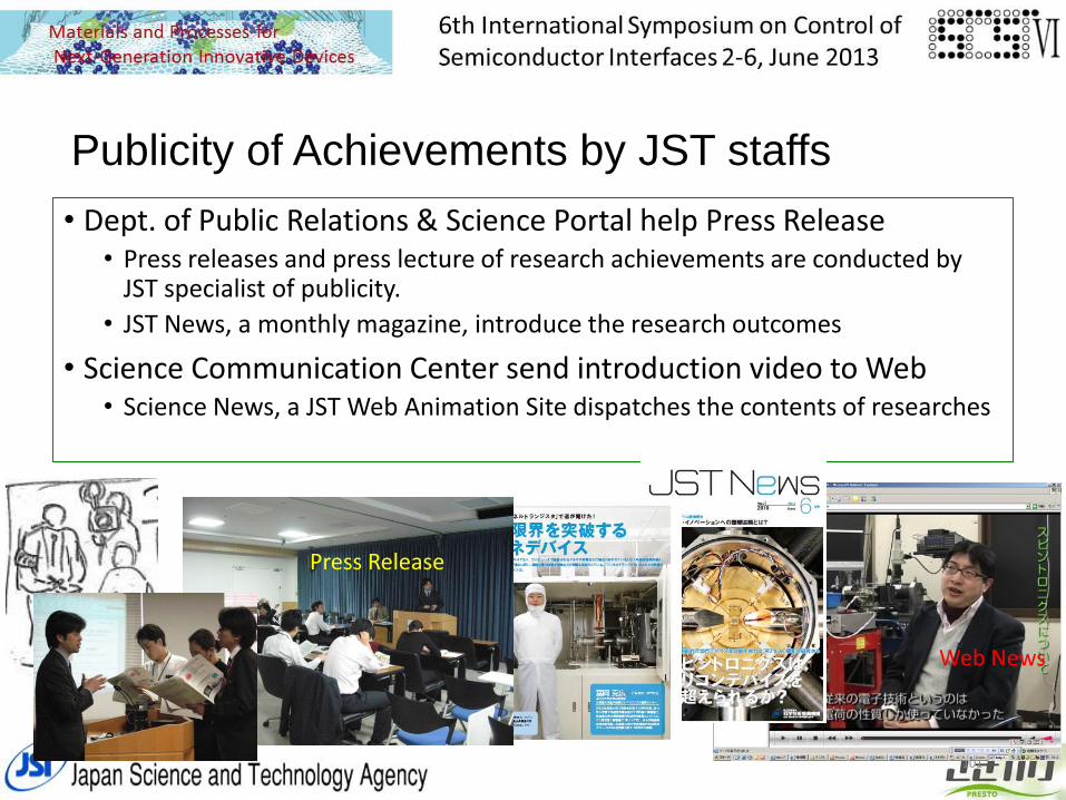
Publicity of Achievements by JST staffs
• Dept. of Public Relations & Science Portal help Press Release• Press releases and press lecture of research achievements are conducted by
JST specialist of publicity.
• JST News, a monthly magazine, introduce the research outcomes
• Science Communication Center send introduction video to Web• Science News, a JST Web Animation Site dispatches the contents of researches
Press Release
Web News
102
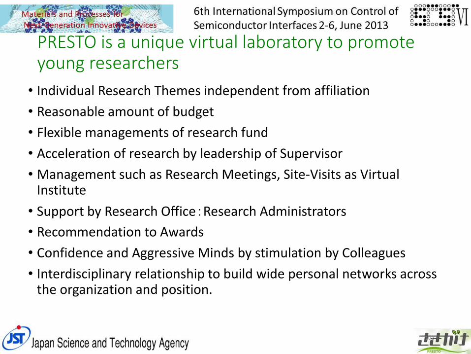
PRESTO is a unique virtual laboratory to promote young researchers
• Individual Research Themes independent from affiliation
• Reasonable amount of budget
• Flexible managements of research fund
• Acceleration of research by leadership of Supervisor
• Management such as Research Meetings, Site-Visits as Virtual Institute
• Support by Research Office:Research Administrators
• Recommendation to Awards
• Confidence and Aggressive Minds by stimulation by Colleagues
• Interdisciplinary relationship to build wide personal networks across the organization and position.
103
Thank you for your attention
appendix
104
105
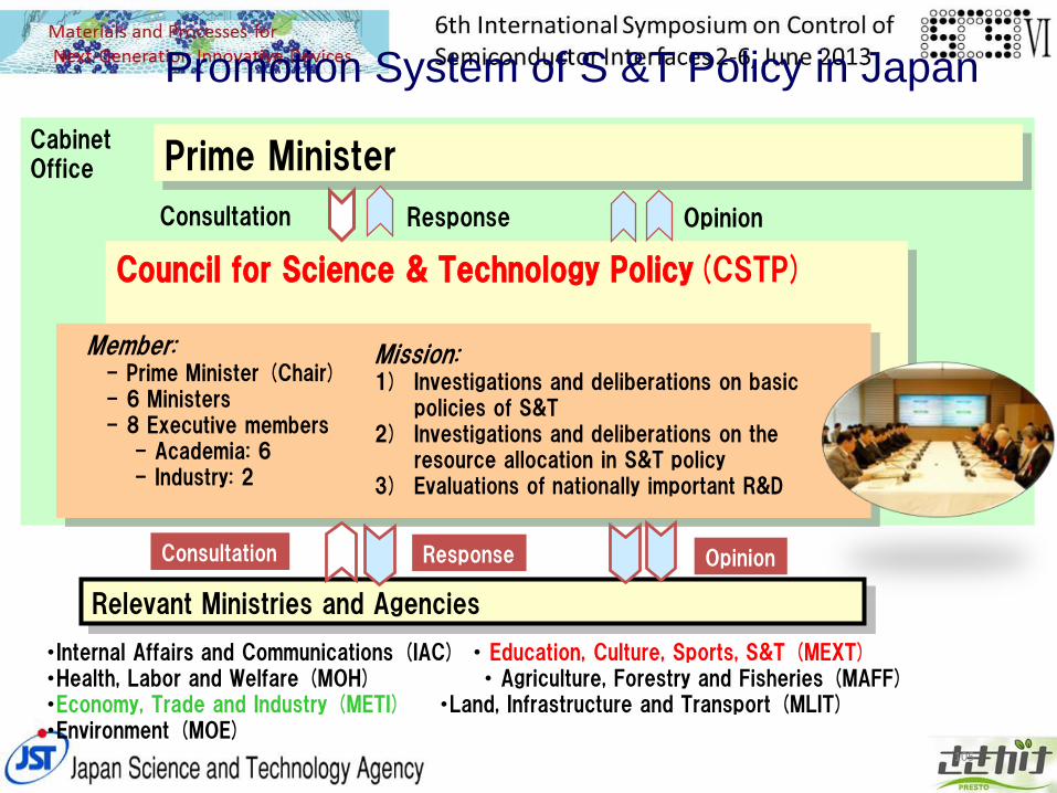
Cabinet Office
Promotion System of S &T Policy in Japan
Prime Minister
Council for Science & Technology Policy(CSTP)
Consultation Response Opinion
Relevant Ministries and Agencies
Opinion
Member:- Prime Minister (Chair)- 6 Ministers- 8 Executive members
- Academia: 6- Industry: 2
Consultation Response
・Internal Affairs and Communications (IAC) ・ Education, Culture, Sports, S&T (MEXT)・Health, Labor and Welfare (MOH) ・ Agriculture, Forestry and Fisheries (MAFF)・Economy, Trade and Industry (METI) ・Land, Infrastructure and Transport (MLIT) ・Environment (MOE)
Mission:1) Investigations and deliberations on basic
policies of S&T2) Investigations and deliberations on the
resource allocation in S&T policy3) Evaluations of nationally important R&D
106
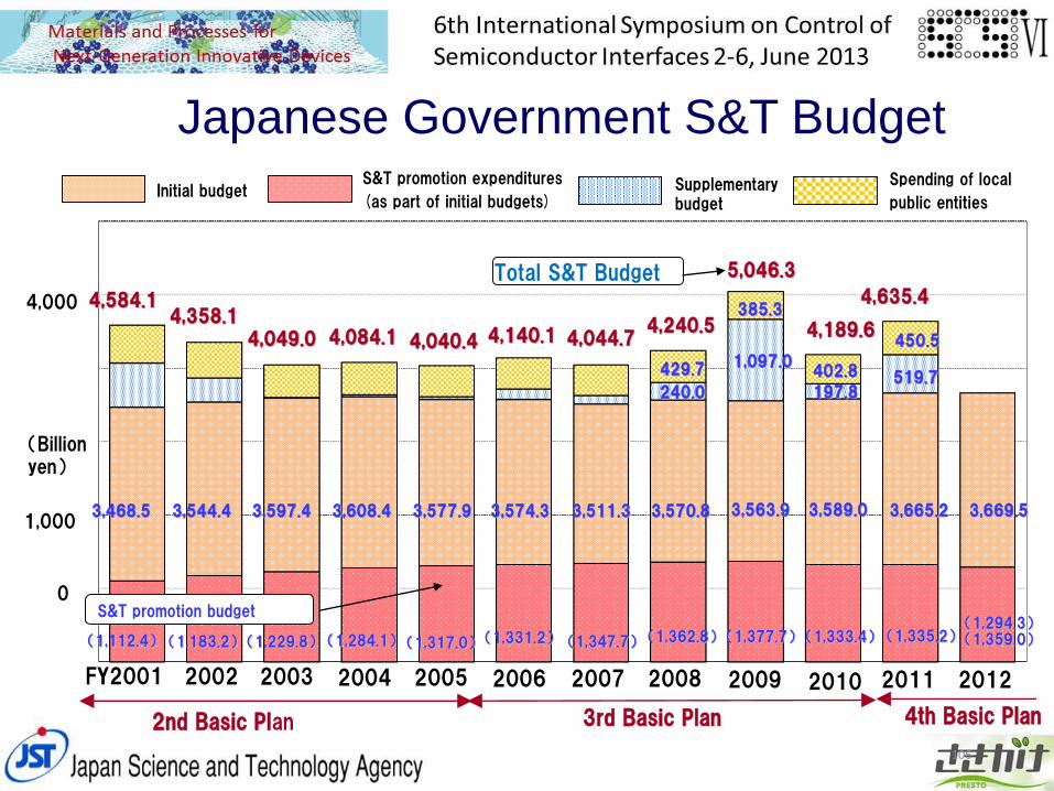
Total S&T budget Total S&T Budget
1,000
0
4,000 4,584.14,358.1
4,049.0 4,084.1 4,040.4 4,140.1
3,511.33,468.5 3,544.4 3,597.4 3,608.4 3,577.9 3,574.3
(1,112.4) (1,183.2) (1,229.8) (1,284.1) (1,317.0) (1,331.2) (1,347.7)
3,570.8
4,044.7
(1,362.8)
4,240.5
(1,377.7)
3,563.9
429.7
240.0
5,046.3
1,097.0
(1,333.4)
3,589.0
385.3
4,189.6
402.8
3,665.2
(1,335.2)
197.8
3,669.5
(1,294.3)(1,359.0)
519.7
450.5
4,635.4
2nd Basic Plan 3rd Basic Plan 4th Basic Plan
(Billion yen)
FY2001
Japanese Government S&T Budget
Initial budgetS&T promotion expenditures
(as part of initial budgets)Supplementary budget
Spending of local
public entities
2002 2003 2004 2005 2006 20082007 2009 2010 2011 2012
S&T promotion budget
107
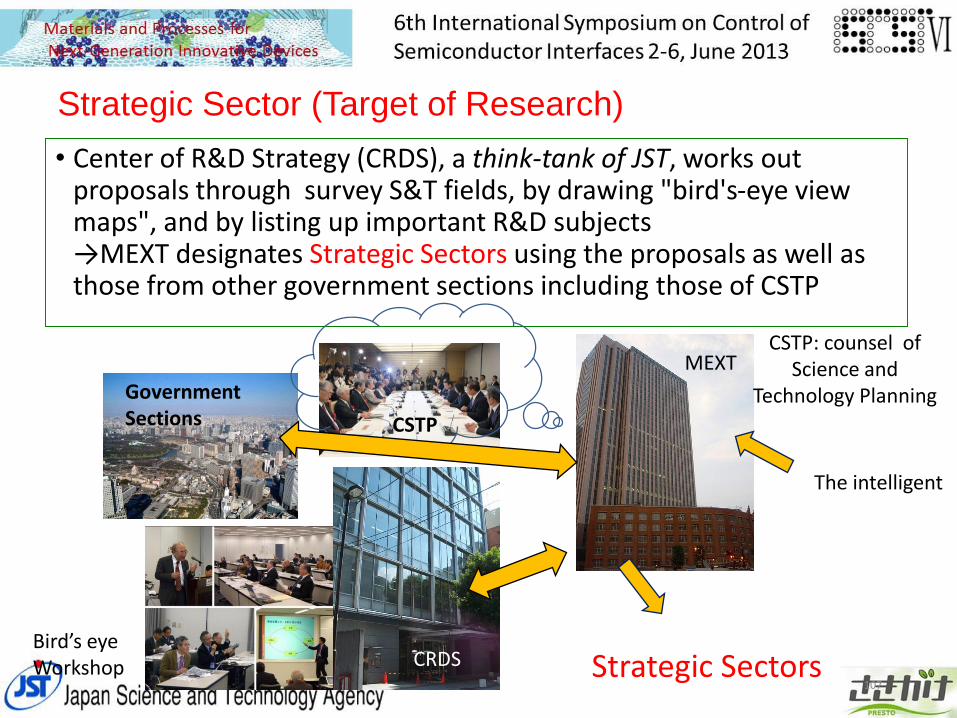
Strategic Sector (Target of Research)
• Center of R&D Strategy (CRDS), a think-tank of JST, works out proposals through survey S&T fields, by drawing "bird's-eye view maps", and by listing up important R&D subjects→MEXT designates Strategic Sectors using the proposals as well as those from other government sections including those of CSTP
文科省CRDS
CSTP
Strategic SectorsBird’s eye Workshop
CSTP: counsel ofScience and
Technology PlanningGovernmentSections
The intelligent
MEXT
108
Research Areas based on the Strategic Sector
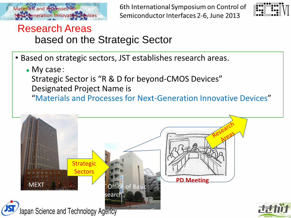
• Based on strategic sectors, JST establishes research areas.
My case:Strategic Sector is “R & D for beyond-CMOS Devices” Designated Project Name is “Materials and Processes for Next-Generation Innovative Devices”
MEXT
Strategic Sectors
JST Office of Basic Research
PD Meeting
Research Office
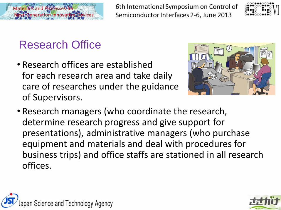
• Research offices are established for each research area and take dailycare of researches under the guidanceof Supervisors.
• Research managers (who coordinate the research, determine research progress and give support for presentations), administrative managers (who purchase equipment and materials and deal with procedures for business trips) and office staffs are stationed in all research offices.
109
110
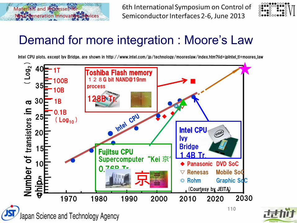
Demand for more integration : Moore’s Law
110
Intel CPU plots, except Iyv Bridge, are shown in http://www.intel.com/jp/technology/mooreslaw/index.htm?iid=jpIntel_tl+moores_law
1970 1980 1990 2000 2010 20200
5
15
10
20
25
30
35( L
og
2 )
◆
◆ Panasonic DVD SoC
▽ Renesas Mobile SoC
◎ Rohm Graphic SoC
(Courtesy by JEITA)
▽◆
◆◆
●●
●
●
●
●
●
▲◎
40
2030
■
Num
ber
of
transi
stors
in a
chip
1B
0.1B
10B
100B
1T
●
Intel CPUIvy Bridge
1.4B Tr.Fujitsu CPUSupercomputer“Kei 京”
0.76B Tr.
Toshiba Flash memory ★
( Log10 )
128G bit NAND@19nm
process
128B Tr.
京
111
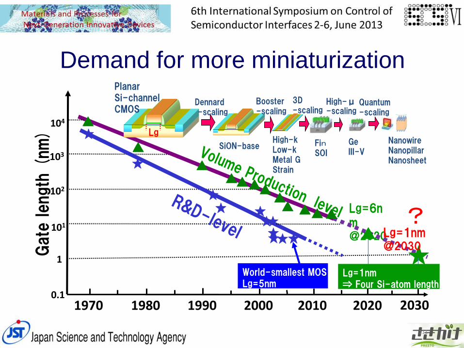
Demand for more miniaturization Gate
length
(nm
)
1
101
★
★
★
▲▲
▲
▲▲
★★
▲▲ ▲
★
★ ★★★★
▲
▲
1970 1980 1990 2000 2010 20200.1
Lg=6nm@2020
World-smallest MOSLg=5nm
★
▲
Quantum-scaling
NanowireNanopillarNanosheet
Dennard-scaling
Booster-scaling
Lg
SiON-baseHigh-kLow-kMetal GStrain
FinSOI
Planar Si-channel CMOS
3D-scaling
▲
放熱経路放熱経路
シングルピラー マルチピラー
2030
Lg=1nm@2030
▲
104
103
102
Lg=1nm⇒ Four Si-atom length
High-μ-scaling
GeIII-V
?