Embed Size (px)
Citation preview
<Project Name> <Date>
MAX® 10 Device Schematic Review Worksheet
This document is intended to help you review your schematic and compare the pin usage against the MAX 10 FPGA Device Family Pin Connection Guidelines (PDF) version 1.5 and other referenced literature for this device family. The technical content is divided into focus areas such as FPGA power supplies, configuration, FPGA I/O, and external memory interfaces.
Within each focus area, there is a table that contains the voltage or pin name for all the dedicated and dual purpose pins for the device family. In some cases, the device density and package combination may not include some of the pins shown in this worksheet, you should cross reference with the pin-out file for your specific device. Links to the device pin-out files are provided at the top of each section.
Before you begin using this worksheet to review your schematic and commit to board layout, Intel highly recommends:
1) Review the latest version of the MAX 10 Device Errata Sheet (PDF) and the Knowledge Database for MAX 10 Device Known Issues.
2) Compile your design in the Quartus® II software to completion.
For example, there are many I/O related placement restrictions and VCCIO requirements for the I/O standards used in the device. If you do not have a complete project, then at a minimum a top-level project should be used with all I/O pins defined, placed, and apply all of the configurable options that you plan to use. All I/O related megafunctions should also be included in the minimal project, including, but not limited to, external memory interfaces, PLLs, altlvds, and altddio. The I/O Analysis tool in the Pin Planner can then be used on the minimal project to validate the pinout in Quartus Prime software to assure there are no conflicts with the device rules and guidelines.
When using the I/O Analysis tool you must ensure there are no errors with your pinout. Additionally, you should check all warning and critical warning messages to evaluate their impact on your design. You can right click your mouse over any warning or critical warning message and select “Help”. This will bring open a new Help window with further information on the cause of the warning, and the action that is required.
MAX 10 Schematic Review Worksheet 1.1 Page 1 of 67 DS-01052-1.1
<Project Name> <Date>
For example, the following warning is generated when a PLL is driven by a global network where the source is a valid dedicated clock input pin, but the pin is not one dedicated to the particular PLL:
Warning: PLL "<PLL Instance Name>" input clock inclk[0] is not fully compensated and may have reduced jitter performance because it is fed by a non-dedicated input
Info: Input port INCLK[0] of node "<PLL Instance Name>" is driven by clock~clkctrl which is OUTCLK output port of Clock Control Block type node clock~clkctrl
The help file provides the following:
CAUSE: The specified PLL's input clock is not driven by a dedicated input pin. As a result, the input clock delay will not be fully compensated by the PLL. Additionally, jitter performance depends on the switching rate of other design elements. This can also occur if a global signal assignment is applied to the clock input pin, which forces the clock to use the non-dedicated global clock network.
ACTION: If you want compensation of the specified input clock or better jitter performance, connect the input clock only to an input pin, or assign the input pin only to a dedicated input clock location for the PLL. If you do not want compensation of the specified input clock, then set the PLL to No Compensation mode.
When assigning the input pin to the proper dedicated clock pin location, refer to MAX 10 Clocking and PLL User Guide (PDF) for the proper port mapping of dedicated clock input pins to PLLs.
There are many reports available for use after a successful compilation or I/O analysis. For example, you can use the “All Package Pins” and “I/O Bank Usage” reports within the Compilation – Fitter – Resource Section to see all of the I/O standards and I/O configurable options that are assigned to all of the pins in your design, as well as view the required VCCIO for each I/O bank. These reports must match your schematic pin connections.
MAX 10 Schematic Review Worksheet 1.1 Page 2 of 67 DS-01052-1.1
<Project Name> <Date>
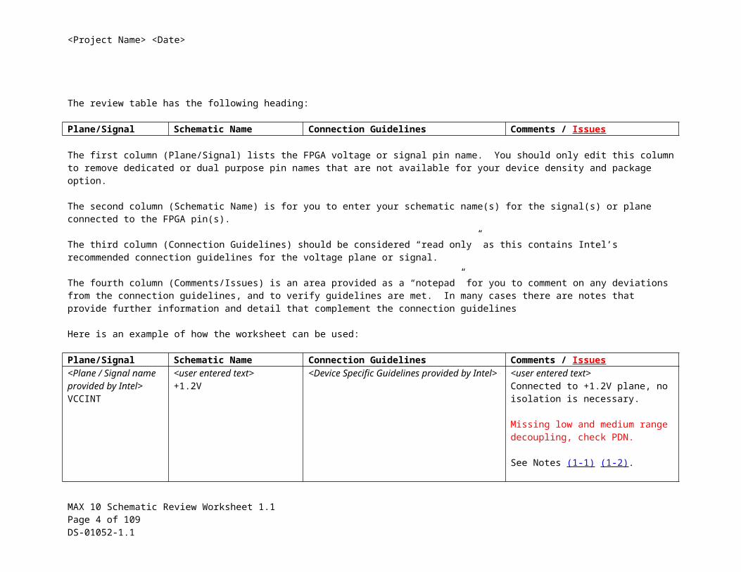
The review table has the following heading:
Plane/Signal Schematic Name Connection Guidelines Comments / Issues
The first column (Plane/Signal) lists the FPGA voltage or signal pin name. You should only edit this column to remove dedicated or dual purpose pin names that are not available for your device density and package option.
The second column (Schematic Name) is for you to enter your schematic name(s) for the signal(s) or plane connected to the FPGA pin(s).
The third column (Connection Guidelines) should be considered “read only” as this contains Intel’s recommended connection guidelines for the voltage plane or signal.
The fourth column (Comments/Issues) is an area provided as a “notepad” for you to comment on any deviations from the connection guidelines, and to verify guidelines are met. In many cases there are notes that provide further information and detail that complement the connection guidelines
Here is an example of how the worksheet can be used:
Plane/Signal Schematic Name Connection Guidelines Comments / Issues<Plane / Signal name provided by Intel>VCCINT
<user entered text>+1.2V
<Device Specific Guidelines provided by Intel>
<user entered text>Connected to +1.2V plane, no isolation is necessary.
Missing low and medium range decoupling, check PDN.
See Notes (1-1) (1-2).
MAX 10 Schematic Review Worksheet 1.1 Page 3 of 67 DS-01052-1.1
<Project Name> <Date>
Legal Note: PLEASE REVIEW THE FOLLOWING TERMS AND CONDITIONS CAREFULLY BEFORE USING THIS SCHEMATIC REVIEW WORKSHEET (“WORKSHEET”) PROVIDED TO YOU. BY USING THIS WORKSHEET, YOU INDICATE YOUR ACCEPTANCE OF SUCH TERMS AND CONDITIONS, WHICH CONSTITUTE THE LICENSE AGREEMENT ("AGREEMENT") BETWEEN YOU AND INTEL CORPORATION OR ITS APPLICABLE SUBSIDIARIES ("INTEL"). 1. Subject to the terms and conditions of this Agreement, Intel grants to you, for no additional fee, a non-exclusive and non-transferable right to use this Worksheet for the sole purpose of verifying the validity of the pin connections of an Intel programmable logic device-based design. You may not use this Worksheet for any other purpose. There are no implied licenses granted under this Agreement, and all rights, except for those granted under this Agreement, remain with Intel. 2. Intel does not guarantee or imply the reliability, or serviceability, of this Worksheet or other items provided as part of this Worksheet. This Worksheet is provided 'AS IS'. INTEL DISCLAIMS ALL WARRANTIES, EXPRESS OR IMPLIED, INCLUDING THE IMPLIED WARRANTIES OF MERCHANTABILITY, FITNESS FOR A PARTICULAR PURPOSE, AND NON-INFRINGEMENT. INTEL HAS NO OBLIGATION TO PROVIDE YOU WITH ANY SUPPORT OR MAINTENANCE. 3. In no event shall the aggregate liability of Intel relating to this Agreement or the subject matter hereof under any legal theory (whether in tort, contract, or otherwise), exceed One Hundred US Dollars (US$100.00). In no event shall Intel be liable for any lost revenue, lost profits, or other consequential, indirect, or special damages caused by your use of this Worksheet even if advised of the possibility of such damages. 4. This Agreement may be terminated by either party for any reason at any time upon 30-days’ prior written notice. This Agreement shall be governed by the laws of the State of California, without regard to conflict of law or choice of law principles. You agree to submit to the exclusive jurisdiction of the courts in the County of Santa Clara, State of California for the resolution of any dispute or claim arising out of or relating to this Agreement. The parties hereby agree that the party who is not the substantially prevailing party with respect to a dispute, claim, or controversy relating to this Agreement shall pay the costs actually incurred by the substantially prevailing party in relation to such dispute, claim, or controversy, including attorneys' fees. Failure to enforce any term or condition of this Agreement shall not be deemed a waiver of the right to later enforce such term or condition or any other term or condition of the Agreement. BY USING THIS WORKSHEET, YOU ACKNOWLEDGE THAT YOU HAVE READ THIS AGREEMENT, UNDERSTAND IT, AND AGREE TO BE BOUND BY ITS TERMS AND CONDITIONS. YOU AND INTEL FURTHER AGREE THAT IT IS THE COMPLETE AND EXCLUSIVE STATEMENT OF THE AGREEMENT BETWEEN YOU AND INTEL, WHICH SUPERSEDES ANY PROPOSAL OR PRIOR AGREEMENT, ORAL OR WRITTEN, AND ANY OTHER COMMUNICATIONS BETWEEN YOU AND INTEL RELATING TO THE SUBJECT MATTER OF THIS AGREEMENT.
MAX 10 Schematic Review Worksheet 1.1 Page 4 of 67 DS-01052-1.1
<Project Name> <Date>
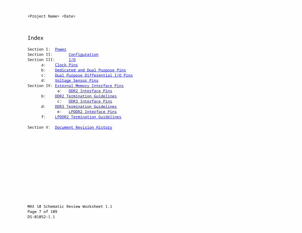
Index
Section I: Power Section II: ConfigurationSection III: I/O
a: Clock Pins b: Dedicated and Dual Purpose Pinsc: Dual Purpose Differential I/O Pinsd: Voltage Sensor Pins
Section IV: External Memory Interface Pins a: DDR2 Interface Pins
b: DDR2 Termination Guidelines c: DDR3 Interface Pins
d: DDR3 Termination Guidelines e: LPDDR2 Interface Pins
f: LPDDR2 Termination Guidelines
Section V: Document Revision History
MAX 10 Schematic Review Worksheet 1.1 Page 5 of 67 DS-01052-1.1
<Project Name> <Date>
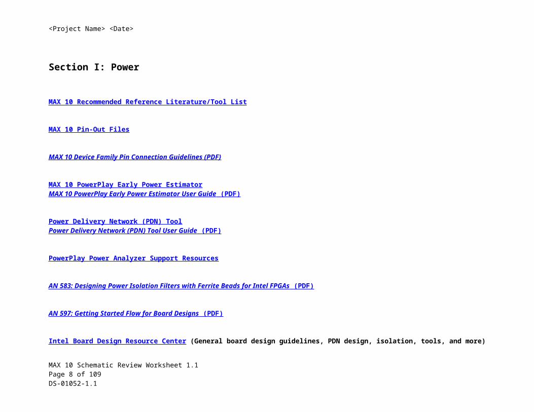
Section I: Power
MAX 10 Recommended Reference Literature/Tool List
MAX 10 Pin-Out Files
MAX 10 Device Family Pin Connection Guidelines (PDF)
MAX 10 PowerPlay Early Power EstimatorMAX 10 PowerPlay Early Power Estimator User Guide (PDF)
Power Delivery Network (PDN) ToolPower Delivery Network (PDN) Tool User Guide (PDF)
PowerPlay Power Analyzer Support Resources
AN 583: Designing Power Isolation Filters with Ferrite Beads for Intel FPGAs (PDF)
AN 597: Getting Started Flow for Board Designs (PDF)
Intel Board Design Resource Center (General board design guidelines, PDN design, isolation, tools, and more)
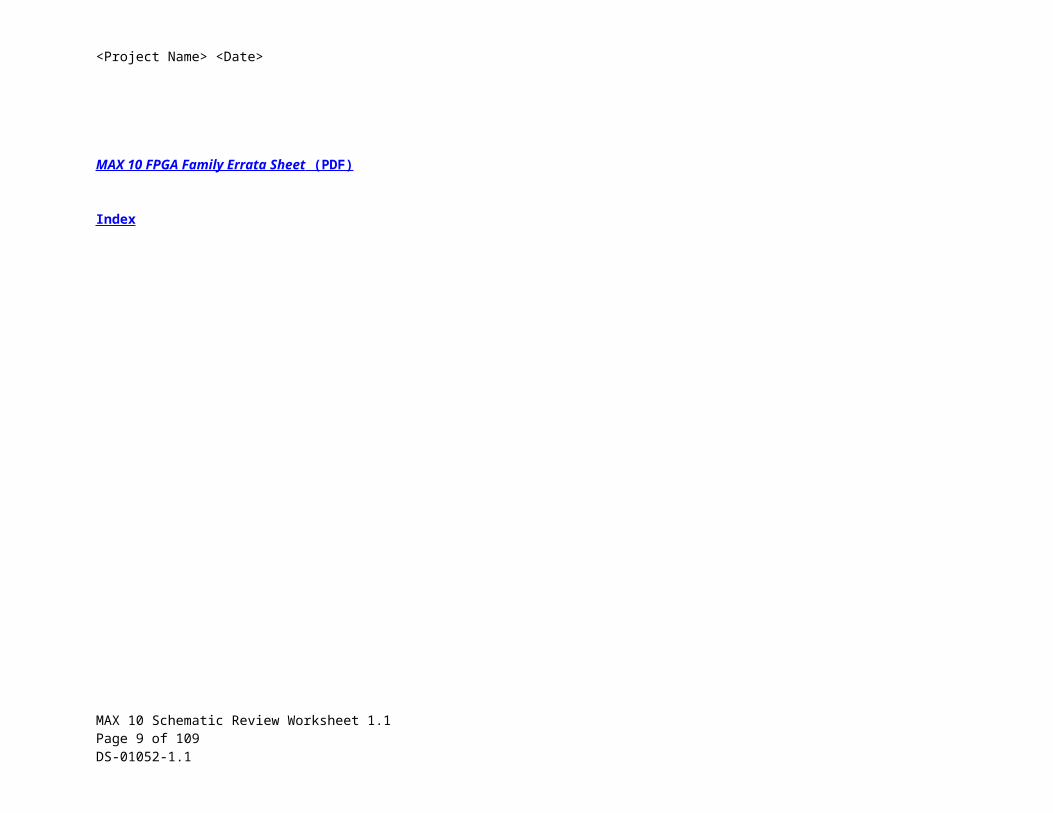
MAX 10 FPGA Family Errata Sheet (PDF)
Index
MAX 10 Schematic Review Worksheet 1.1 Page 6 of 67 DS-01052-1.1
<Project Name> <Date>
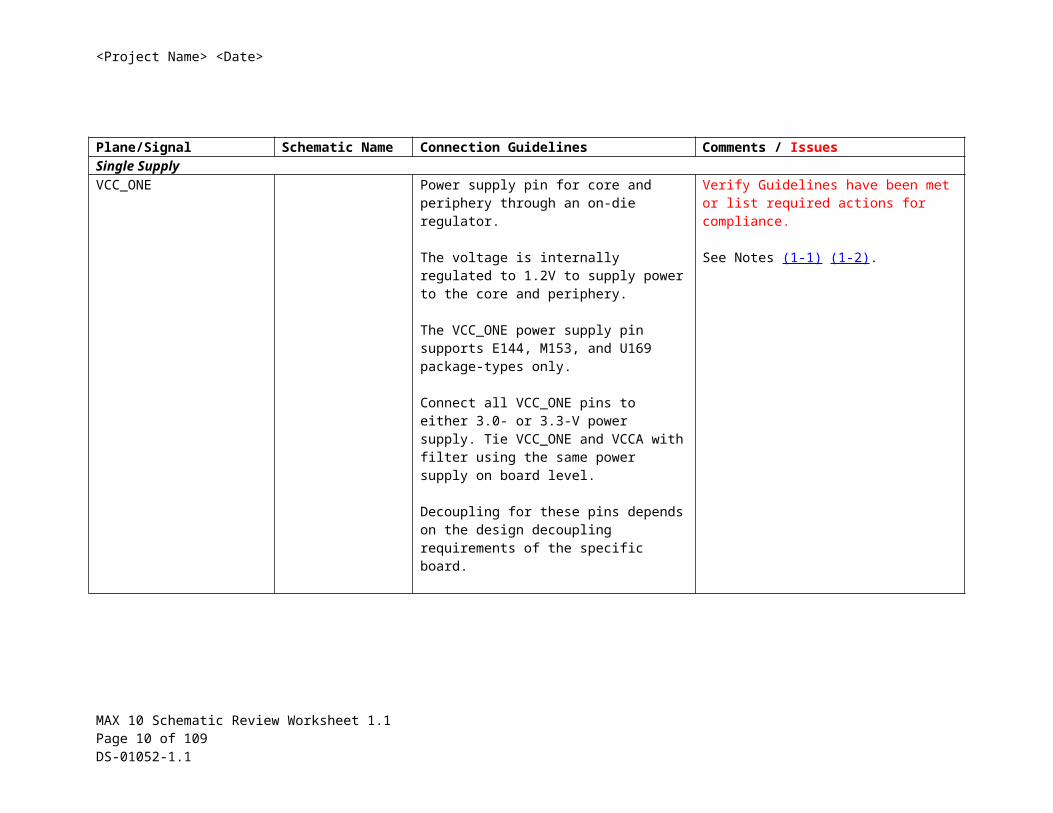
Plane/Signal Schematic Name Connection Guidelines Comments / IssuesSingle SupplyVCC_ONE Power supply pin for core and periphery
through an on-die regulator.
The voltage is internally regulated to 1.2V to supply power to the core and periphery.
The VCC_ONE power supply pin supports E144, M153, and U169 package-types only.
Connect all VCC_ONE pins to either 3.0- or 3.3-V power supply. Tie VCC_ONE and VCCA with filter using the same power supply on board level.
Decoupling for these pins depends on the design decoupling requirements of the specific board.
Verify Guidelines have been met or list required actions for compliance.
See Notes (1-1) (1-2).
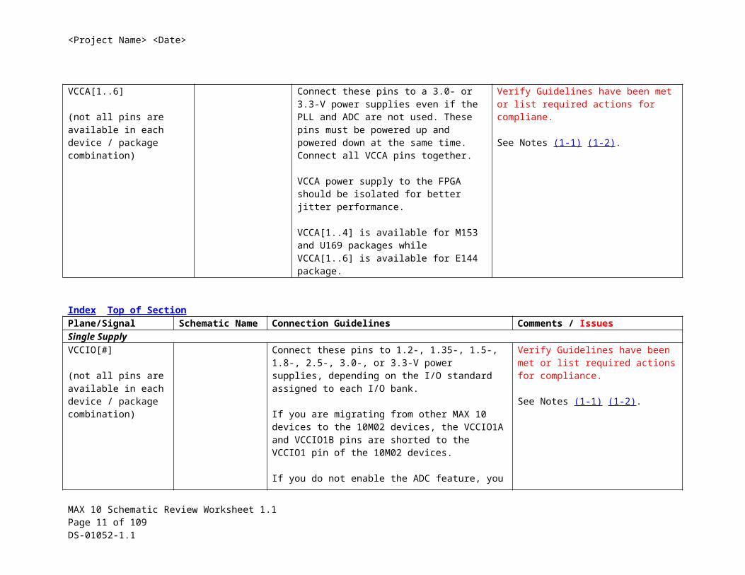
VCCA[1..6]
(not all pins are available in each device / package combination)
Connect these pins to a 3.0- or 3.3-V power supplies even if the PLL and ADC are not used. These pins must be powered up and powered down at the same time. Connect all VCCA pins together.
VCCA power supply to the FPGA should be isolated for better jitter performance.
VCCA[1..4] is available for M153 and U169 packages while VCCA[1..6] is available for E144 package.
Verify Guidelines have been met or list required actions for compliane.
See Notes (1-1) (1-2).
Index Top of SectionPlane/Signal Schematic Name Connection Guidelines Comments / Issues
MAX 10 Schematic Review Worksheet 1.1 Page 7 of 67 DS-01052-1.1
<Project Name> <Date>
Single SupplyVCCIO[#]
(not all pins are available in each device / package combination)
Connect these pins to 1.2-, 1.35-, 1.5-, 1.8-, 2.5-, 3.0-, or 3.3-V power supplies, depending on the I/O standard assigned to each I/O bank.
If you are migrating from other MAX 10 devices to the 10M02 devices, the VCCIO1A and VCCIO1B pins are shorted to the VCCIO1 pin of the 10M02 devices.
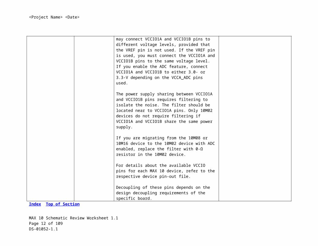
If you do not enable the ADC feature, you may connect VCCIO1A and VCCIO1B pins to different voltage levels, provided that the VREF pin is not used. If the VREF pin is used, you must connect the VCCIO1A and VCCIO1B pins to the same voltage level.If you enable the ADC feature, connect VCCIO1A and VCCIO1B to either 3.0- or 3.3-V depending on the VCCA_ADC pins used.
The power supply sharing between VCCIO1A and VCCIO1B pins requires filtering to isolate the noise. The filter should be located near to VCCIO1A pins. Only 10M02 devices do not require filtering if VCCIO1A and VCCIO1B share the same power supply.
If you are migrating from the 10M08 or 10M16 device to the 10M02 device with ADC enabled, replace the filter with 0-Ω resistor in the 10M02 device.
For details about the available VCCIO pins for each MAX 10 device, refer to the respective device pin-out file.
Decoupling of these pins depends on the design decoupling requirements of the specific board.
Verify Guidelines have been met or list required actions for compliance.
See Notes (1-1) (1-2).
Index Top of Section
MAX 10 Schematic Review Worksheet 1.1 Page 8 of 67 DS-01052-1.1
<Project Name> <Date>
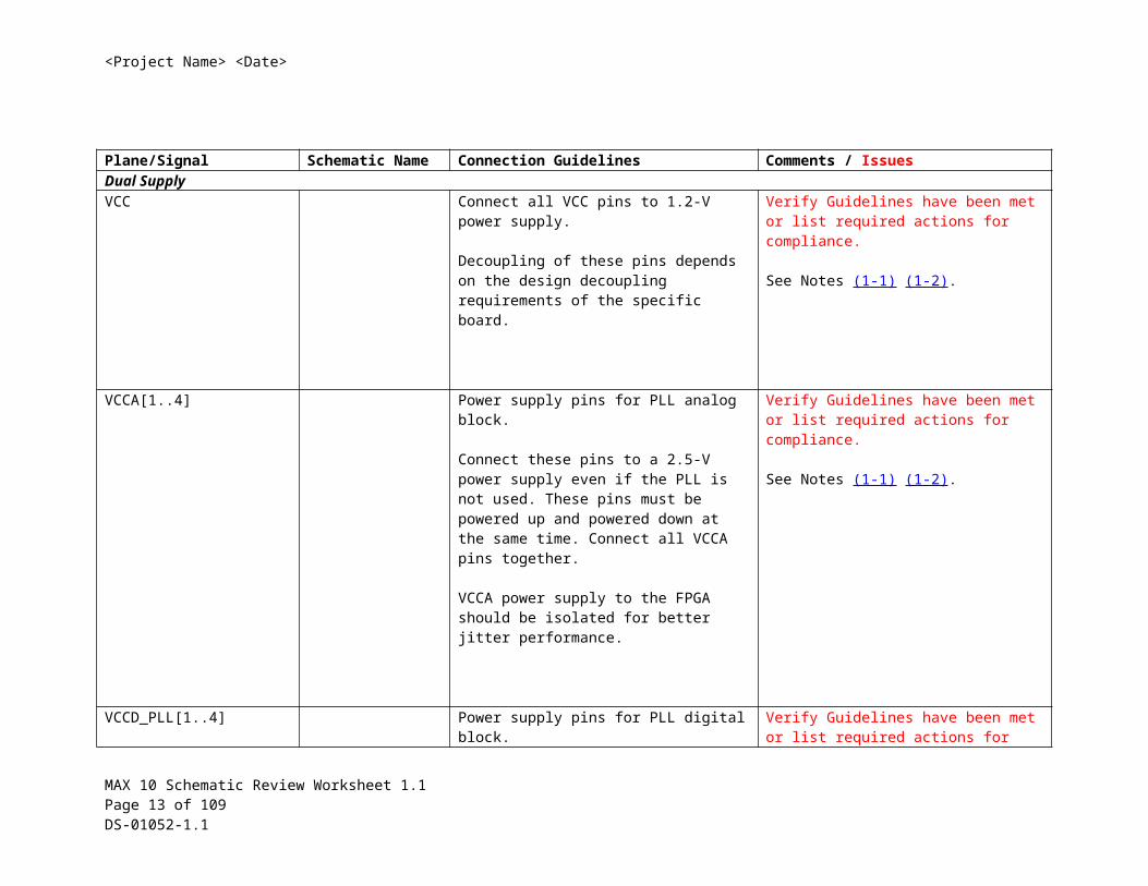
Plane/Signal Schematic Name Connection Guidelines Comments / IssuesDual SupplyVCC Connect all VCC pins to 1.2-V power supply.
Decoupling of these pins depends on the design decoupling requirements of the specific board.
Verify Guidelines have been met or list required actions for compliance.
See Notes (1-1) (1-2).
VCCA[1..4] Power supply pins for PLL analog block.
Connect these pins to a 2.5-V power supply even if the PLL is not used. These pins must be powered up and powered down at the same time. Connect all VCCA pins together.
VCCA power supply to the FPGA should be isolated for better jitter performance.
Verify Guidelines have been met or list required actions for compliance.
See Notes (1-1) (1-2).
VCCD_PLL[1..4] Power supply pins for PLL digital block.
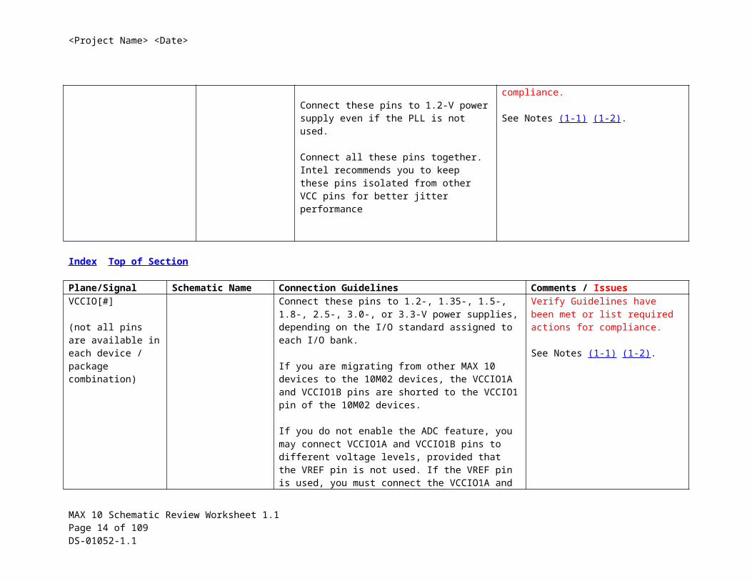
Connect these pins to 1.2-V power supply even if the PLL is not used.
Connect all these pins together. Intel recommends you to keep these pins isolated from other VCC pins for better jitter performance
Verify Guidelines have been met or list required actions for compliance.
See Notes (1-1) (1-2).
Index Top of Section
MAX 10 Schematic Review Worksheet 1.1 Page 9 of 67 DS-01052-1.1
<Project Name> <Date>
Plane/Signal Schematic Name Connection Guidelines Comments / IssuesVCCIO[#]
(not all pins are available in each device / package combination)
Connect these pins to 1.2-, 1.35-, 1.5-, 1.8-, 2.5-, 3.0-, or 3.3-V power supplies, depending on the I/O standard assigned to each I/O bank.
If you are migrating from other MAX 10 devices to the 10M02 devices, the VCCIO1A and VCCIO1B pins are shorted to the VCCIO1 pin of the 10M02 devices.
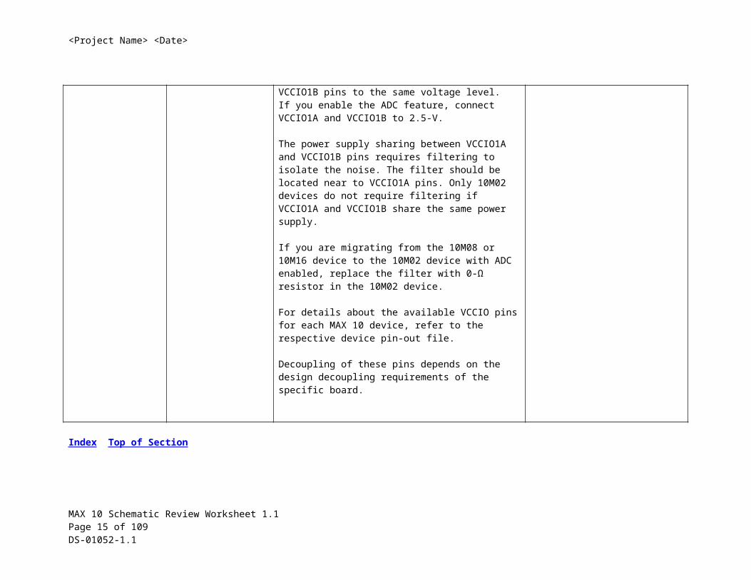
If you do not enable the ADC feature, you may connect VCCIO1A and VCCIO1B pins to different voltage levels, provided that the VREF pin is not used. If the VREF pin is used, you must connect the VCCIO1A and VCCIO1B pins to the same voltage level.If you enable the ADC feature, connect VCCIO1A and VCCIO1B to 2.5-V.
The power supply sharing between VCCIO1A and VCCIO1B pins requires filtering to isolate the noise. The filter should be located near to VCCIO1A pins. Only 10M02 devices do not require filtering if VCCIO1A and VCCIO1B share the same power supply.
If you are migrating from the 10M08 or 10M16 device to the 10M02 device with ADC enabled, replace the filter with 0-Ω resistor in the 10M02 device.
For details about the available VCCIO pins for each MAX 10 device, refer to the respective device pin-out file.
Decoupling of these pins depends on the design decoupling requirements of the specific board.
Verify Guidelines have been met or list required actions for compliance.
See Notes (1-1) (1-2).
Index Top of Section
MAX 10 Schematic Review Worksheet 1.1 Page 10 of 67 DS-01052-1.1
<Project Name> <Date>
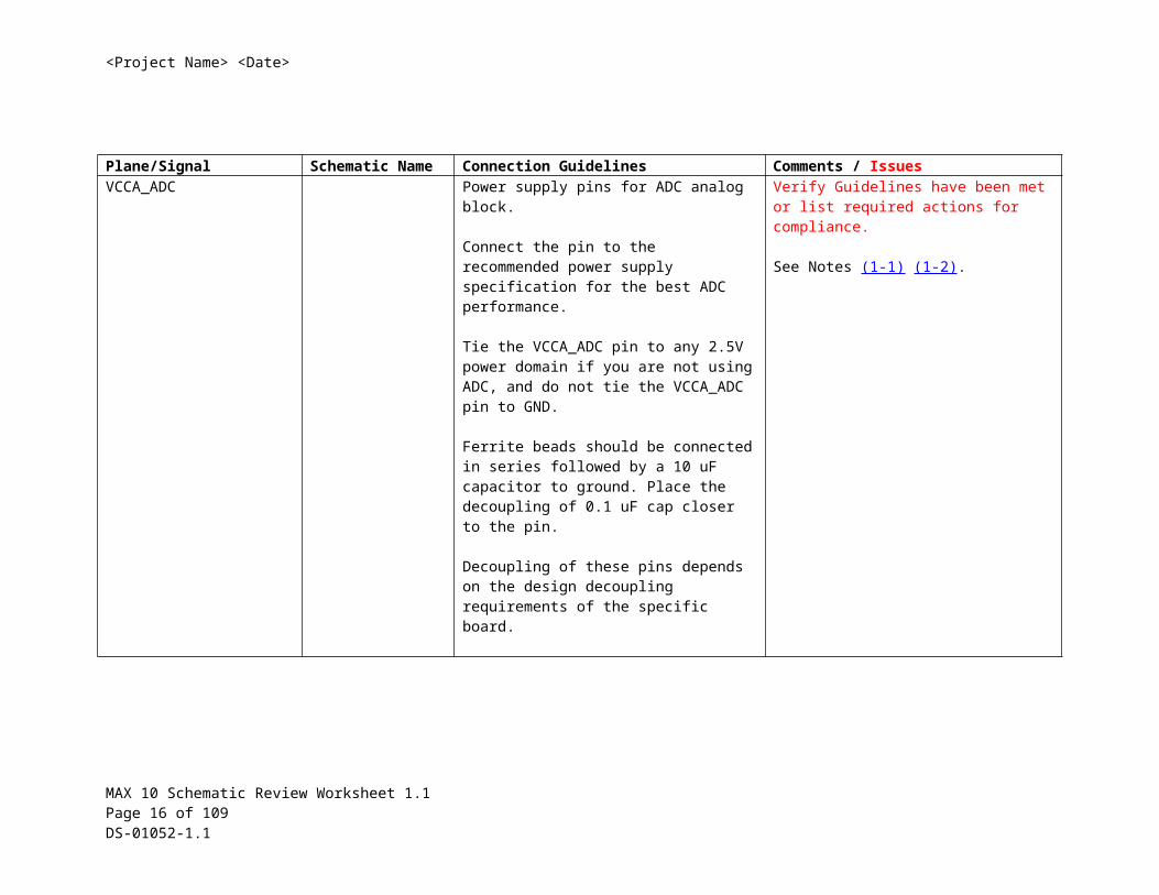
Plane/Signal Schematic Name Connection Guidelines Comments / IssuesVCCA_ADC Power supply pins for ADC analog block.
Connect the pin to the recommended power supply specification for the best ADC performance.
Tie the VCCA_ADC pin to any 2.5V power domain if you are not using ADC, and do not tie the VCCA_ADC pin to GND.
Ferrite beads should be connected in series followed by a 10 uF capacitor to ground. Place the decoupling of 0.1 uF cap closer to the pin.
Decoupling of these pins depends on the design decoupling requirements of the specific board.
Verify Guidelines have been met or list required actions for compliance.
See Notes (1-1) (1-2).
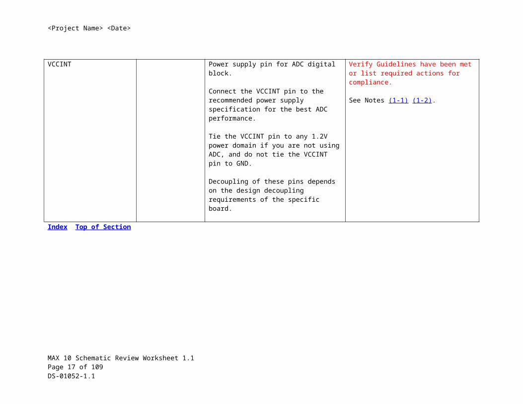
VCCINT Power supply pin for ADC digital block.
Connect the VCCINT pin to the recommended power supply specification for the best ADC performance.
Tie the VCCINT pin to any 1.2V power domain if you are not using ADC, and do not tie the VCCINT pin to GND.
Decoupling of these pins depends on the design decoupling requirements of the specific board.
Verify Guidelines have been met or list required actions for compliance.
See Notes (1-1) (1-2).
Index Top of Section
MAX 10 Schematic Review Worksheet 1.1 Page 11 of 67 DS-01052-1.1
<Project Name> <Date>
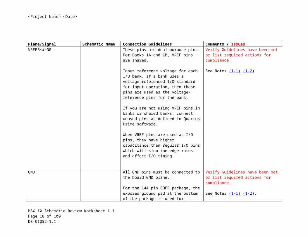
Plane/Signal Schematic Name Connection Guidelines Comments / IssuesVREFB<#>N0 These pins are dual-purpose pins. For Banks
1A and 1B, VREF pins are shared.
Input reference voltage for each I/O bank. If a bank uses a voltage referenced I/O standard for input operation, then these pins are used as the voltage-reference pins for the bank.
If you are not using VREF pins in banks or shared banks, connect unused pins as defined in Quartus Prime software.
When VREF pins are used as I/O pins, they have higher capacitance than regular I/O pins which will slow the edge rates and affect I/O timing.
Verify Guidelines have been met or list required actions for compliance.
See Notes (1-1) (1-2).
GND All GND pins must be connected to the board GND plane.
For the 144 pin EQFP package, the exposed ground pad at the bottom of the package is used for electrical connectivity and must be connected to GND.
Verify Guidelines have been met or list required actions for compliance.
See Notes (1-1) (1-2).
Index Top of Section
MAX 10 Schematic Review Worksheet 1.1 Page 12 of 67 DS-01052-1.1
<Project Name> <Date>
Notes:
1-1. This worksheet does not calculate required decoupling, it is expected the designer will select decoupling based on analysis of power required and impedance of power path required based on static and switching current values. Refer to Intel’s Power Delivery Network (PDN) Tool for further information.
Capacitance values for the power supply should be selected after consideration of the amount of power they need to supply over the frequency of operation of the particular circuit being decoupled. A target impedance for the power plane should be calculated based on current draw and voltage drop requirements of the device/supply. The power plane should then be decoupled using the appropriate number of capacitors. On-board capacitors do not decouple higher than 100 MHz due to “Equivalent Series Inductance” of the mounting of the packages. Proper board design techniques such as interplane capacitance with low inductance should be considered for higher frequency decoupling.
Intel highly recommends using an independent PCB via for each independent power or ground ball on the package. Sharing power or ground pin vias on the PCB could lead to noise coupling into the device and result in reduced jitter performance.
1-2. This worksheet does not include power estimation for the different power supplies provided. Ensure each power supply is adequate for the device current requirements. Refer to Intel’s Early Power Estimation Tools and PowerPlay Power Analyzer Support Resources for further guidance.
1-3. Example 1~6 in MAX 10 FPGA Device Family Pin Connection Guidelines (PDF) show power supply sharing guidelines.
Use Intel’s Early Power Estimation Tools to ensure the junction temperature of the device is within operating specifications based on your design activity.
Index Top of Section
MAX 10 Schematic Review Worksheet 1.1 Page 13 of 67 DS-01052-1.1
<Project Name> <Date>
Additional Comments:
Index Top of Section
MAX 10 Schematic Review Worksheet 1.1 Page 14 of 67 DS-01052-1.1
<Project Name> <Date>
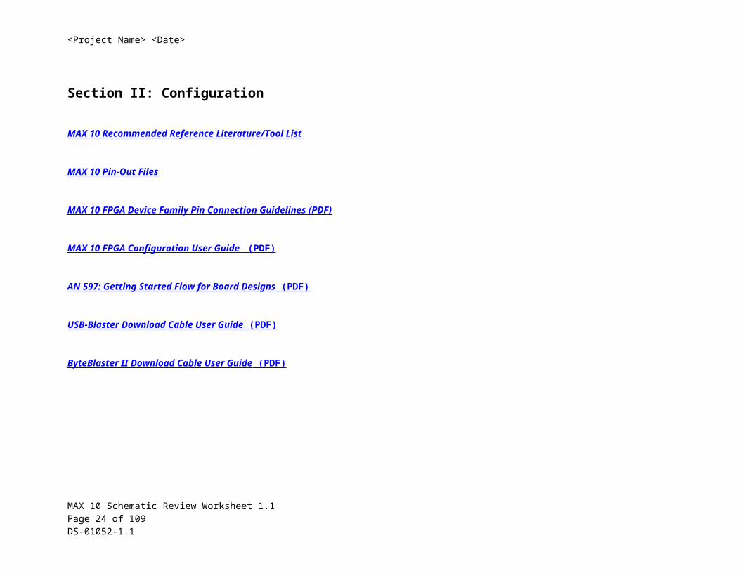
Section II: Configuration
MAX 10 Recommended Reference Literature/Tool List
MAX 10 Pin-Out Files
MAX 10 FPGA Device Family Pin Connection Guidelines (PDF)
MAX 10 FPGA Configuration User Guide (PDF)
AN 597: Getting Started Flow for Board Designs (PDF)
USB-Blaster Download Cable User Guide (PDF)
ByteBlaster II Download Cable User Guide (PDF)
Index
MAX 10 Schematic Review Worksheet 1.1 Page 15 of 67 DS-01052-1.1
<Project Name> <Date>
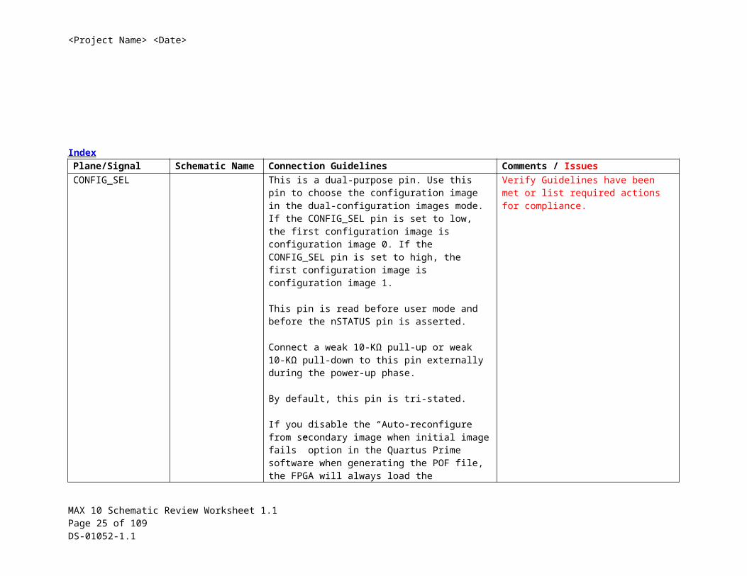
Plane/Signal Schematic Name Connection Guidelines Comments / IssuesCONFIG_SEL This is a dual-purpose pin. Use this pin to choose the
configuration image in the dual-configuration images mode. If the CONFIG_SEL pin is set to low, the first configuration image is configuration image 0. If the CONFIG_SEL pin is set to high, the first configuration image is configuration image 1.
This pin is read before user mode and before the nSTATUS pin is asserted.
Connect a weak 10-KΩ pull-up or weak 10-KΩ pull-down to this pin externally during the power-up phase.
By default, this pin is tri-stated.
If you disable the “Auto-reconfigure from secondary image when initial image fails” option in the Quartus Prime software when generating the POF file, the FPGA will always load the configuration image 0 without sampling the physical CONFIG_SEL pin during power up.
Verify Guidelines have been met or list required actions for compliance.
Index Top of Section
MAX 10 Schematic Review Worksheet 1.1 Page 16 of 67 DS-01052-1.1
<Project Name> <Date>
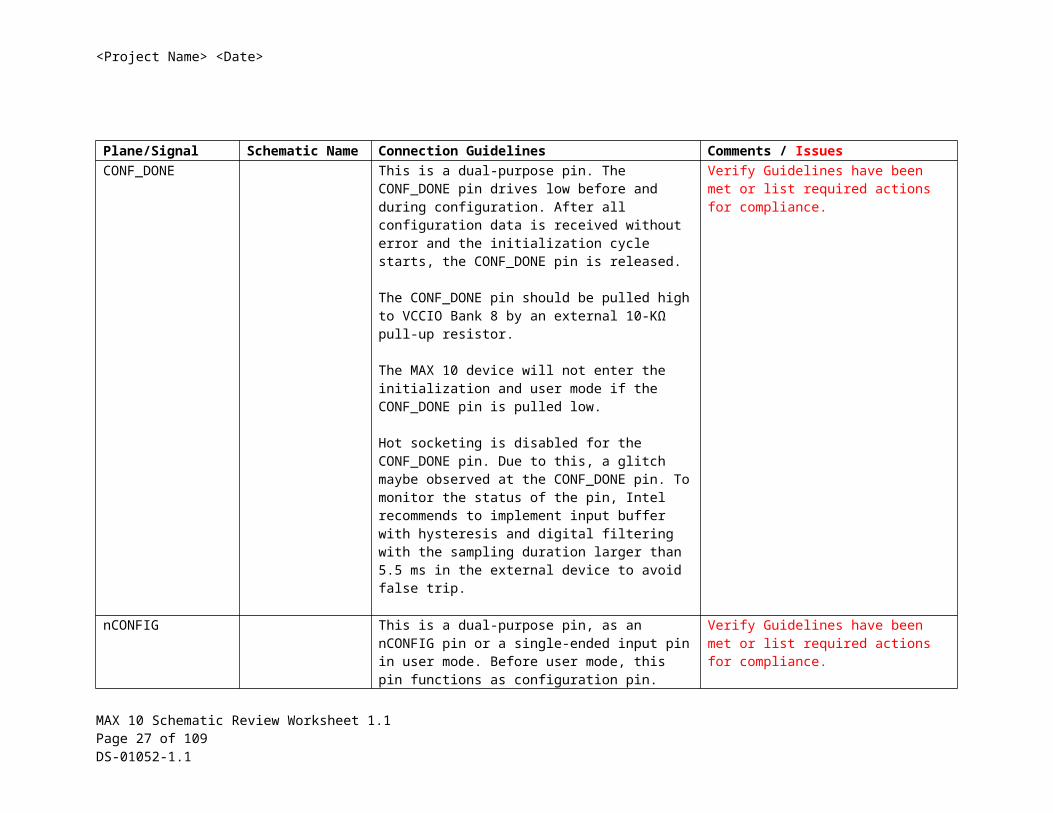
Plane/Signal Schematic Name Connection Guidelines Comments / IssuesCONF_DONE This is a dual-purpose pin. The CONF_DONE pin
drives low before and during configuration. After all configuration data is received without error and the initialization cycle starts, the CONF_DONE pin is released.
The CONF_DONE pin should be pulled high to VCCIO Bank 8 by an external 10-KΩ pull-up resistor.
The MAX 10 device will not enter the initialization and user mode if the CONF_DONE pin is pulled low.
Hot socketing is disabled for the CONF_DONE pin. Due to this, a glitch maybe observed at the CONF_DONE pin. To monitor the status of the pin, Intel recommends to implement input buffer with hysteresis and digital filtering with the sampling duration larger than 5.5 ms in the external device to avoid false trip.
Verify Guidelines have been met or list required actions for compliance.
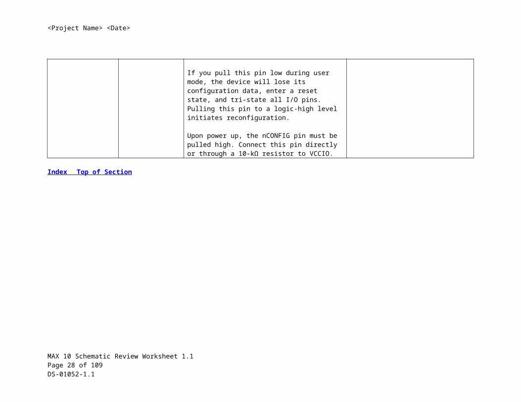
nCONFIG This is a dual-purpose pin, as an nCONFIG pin or a single-ended input pin in user mode. Before user mode, this pin functions as configuration pin.
If you pull this pin low during user mode, the device will lose its configuration data, enter a reset state, and tri-state all I/O pins. Pulling this pin to a logic-high level initiates reconfiguration.
Upon power up, the nCONFIG pin must be pulled high. Connect this pin directly or through a 10-kΩ resistor to VCCIO.
Verify Guidelines have been met or list required actions for compliance.
Index Top of Section
MAX 10 Schematic Review Worksheet 1.1 Page 17 of 67 DS-01052-1.1
<Project Name> <Date>
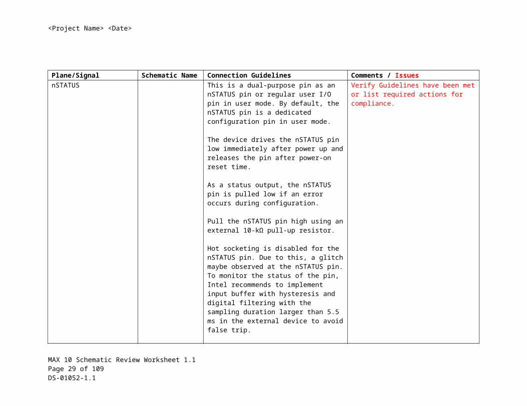
Plane/Signal Schematic Name Connection Guidelines Comments / IssuesnSTATUS This is a dual-purpose pin as an nSTATUS
pin or regular user I/O pin in user mode. By default, the nSTATUS pin is a dedicated configuration pin in user mode.
The device drives the nSTATUS pin low immediately after power up and releases the pin after power-on reset time.
As a status output, the nSTATUS pin is pulled low if an error occurs during configuration.
Pull the nSTATUS pin high using an external 10-kΩ pull-up resistor.
Hot socketing is disabled for the nSTATUS pin. Due to this, a glitch maybe observed at the nSTATUS pin. To monitor the status of the pin, Intel recommends to implement input buffer with hysteresis and digital filtering with the sampling duration larger than 5.5 ms in the external device to avoid false trip.
Verify Guidelines have been met or list required actions for compliance.
Index Top of Section
MAX 10 Schematic Review Worksheet 1.1 Page 18 of 67 DS-01052-1.1
<Project Name> <Date>
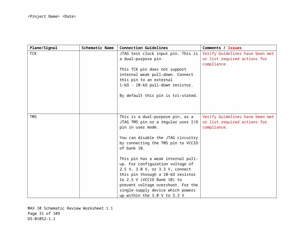
Plane/Signal Schematic Name Connection Guidelines Comments / IssuesTCK JTAG test clock input pin. This is a dual-
purpose pin.
This TCK pin does not support internal weak pull-down. Connect this pin to an external 1-kΩ - 10-kΩ pull-down resistor.
By default this pin is tri-stated.
Verify Guidelines have been met or list required actions for compliance.
TMS This is a dual-purpose pin, as a JTAG TMS pin or a regular user I/O pin in user mode.
You can disable the JTAG circuitry by connecting the TMS pin to VCCIO of bank 1B.
This pin has a weak internal pull-up. For configuration voltage of 2.5 V, 3.0 V, or 3.3 V, connect this pin through a 10-kΩ resistor to 2.5 V (VCCIO Bank 1B) to prevent voltage overshoot. For the single-supply device which powers up within the 3.0 V to 3.3 V range, Intel recommends you to add an external capacitor or diode to reduce voltage overshoot. For configuration voltage of 1.5 V and 1.8 V, connect this pin through a 10-kΩ resistor to VCCIO Bank 1B supply.
Verify Guidelines have been met or list required actions for compliance.
MAX 10 Schematic Review Worksheet 1.1 Page 19 of 67 DS-01052-1.1
<Project Name> <Date>
Index Top of Section
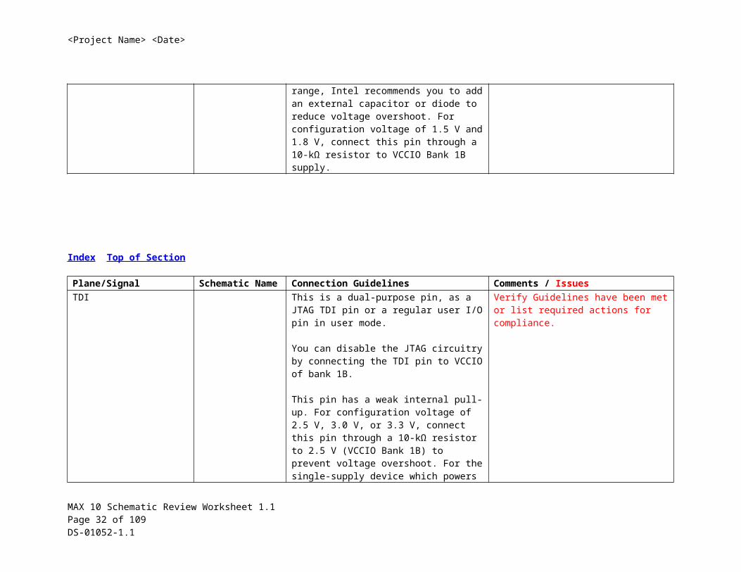
Plane/Signal Schematic Name Connection Guidelines Comments / IssuesTDI This is a dual-purpose pin, as a JTAG TDI pin
or a regular user I/O pin in user mode.
You can disable the JTAG circuitry by connecting the TDI pin to VCCIO of bank 1B.
This pin has a weak internal pull-up. For configuration voltage of 2.5 V, 3.0 V, or 3.3 V, connect this pin through a 10-kΩ resistor to 2.5 V (VCCIO Bank 1B) to prevent voltage overshoot. For the single-supply device which powers up within the 3.0 V to 3.3 V range, Intel recommends you to add an external capacitor or diode to reduce voltage overshoot. For configuration voltage of 1.5 V and 1.8 V, connect this pin through a 10-kΩ resistor to VCCIO Bank 1B supply.
Verify Guidelines have been met or list required actions for compliance.
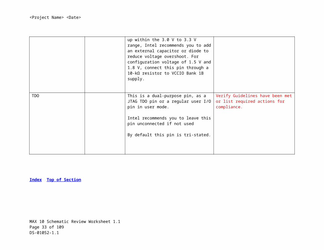
TDO This is a dual-purpose pin, as a JTAG TDO pin or a regular user I/O pin in user mode.
Intel recommends you to leave this pin unconnected if not used
By default this pin is tri-stated.
Verify Guidelines have been met or list required actions for compliance.
Index Top of Section
MAX 10 Schematic Review Worksheet 1.1 Page 20 of 67 DS-01052-1.1
<Project Name> <Date>
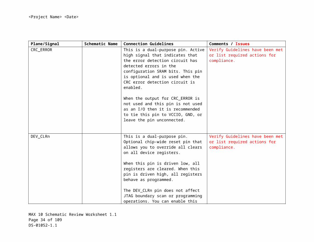
Plane/Signal Schematic Name Connection Guidelines Comments / IssuesCRC_ERROR This is a dual-purpose pin. Active high signal
that indicates that the error detection circuit has detected errors in the configuration SRAM bits. This pin is optional and is used when the CRC error detection circuit is enabled.
When the output for CRC_ERROR is not used and this pin is not used as an I/O then it is recommended to tie this pin to VCCIO, GND, or leave the pin unconnected.
Verify Guidelines have been met or list required actions for compliance.
DEV_CLRn This is a dual-purpose pin. Optional chip-wide reset pin that allows you to override all clears on all device registers.
When this pin is driven low, all registers are cleared. When this pin is driven high, all registers behave as programmed.
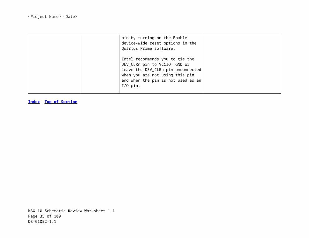
The DEV_CLRn pin does not affect JTAG boundary scan or programming operations. You can enable this pin by turning on the Enable device-wide reset options in the Quartus Prime software.
Intel recommends you to tie the DEV_CLRn pin to VCCIO, GND or leave the DEV_CLRn pin unconnected when you are not using this pin and when the pin is not used as an I/O pin.
Verify Guidelines have been met or list required actions for compliance.
Index Top of Section
MAX 10 Schematic Review Worksheet 1.1 Page 21 of 67 DS-01052-1.1
<Project Name> <Date>
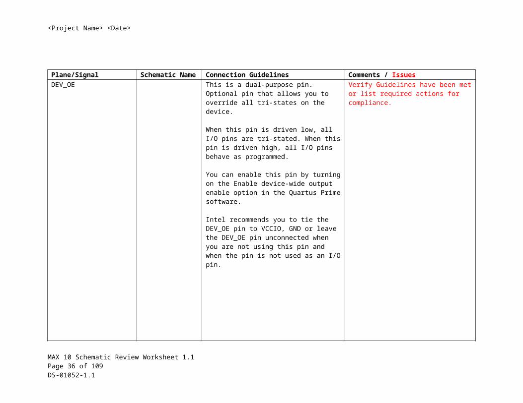
Plane/Signal Schematic Name Connection Guidelines Comments / IssuesDEV_OE This is a dual-purpose pin. Optional pin that
allows you to override all tri-states on the device.
When this pin is driven low, all I/O pins are tri-stated. When this pin is driven high, all I/O pins behave as programmed.
You can enable this pin by turning on the Enable device-wide output enable option in the Quartus Prime software.
Intel recommends you to tie the DEV_OE pin to VCCIO, GND or leave the DEV_OE pin unconnected when you are not using this pin and when the pin is not used as an I/O pin.
Verify Guidelines have been met or list required actions for compliance.
Index Top of Section
MAX 10 Schematic Review Worksheet 1.1 Page 22 of 67 DS-01052-1.1
<Project Name> <Date>
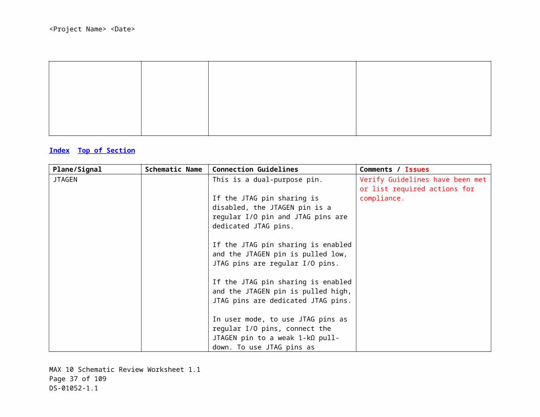
Plane/Signal Schematic Name Connection Guidelines Comments / IssuesJTAGEN This is a dual-purpose pin.
If the JTAG pin sharing is disabled, the JTAGEN pin is a regular I/O pin and JTAG pins are dedicated JTAG pins.
If the JTAG pin sharing is enabled and the JTAGEN pin is pulled low, JTAG pins are regular I/O pins.
If the JTAG pin sharing is enabled and the JTAGEN pin is pulled high, JTAG pins are dedicated JTAG pins.
In user mode, to use JTAG pins as regular I/O pins, connect the JTAGEN pin to a weak 1-kΩ pull-down. To use JTAG pins as dedicated pins, connect the JTAGEN pin to a weak 10-kΩ pull-up.
Verify Guidelines have been met or list required actions for compliance.
Index Top of Section
MAX 10 Schematic Review Worksheet 1.1 Page 23 of 67 DS-01052-1.1
<Project Name> <Date>
Additional Comments:
Index Top of Section
MAX 10 Schematic Review Worksheet 1.1 Page 24 of 67 DS-01052-1.1
<Project Name> <Date>
Section III: I/O
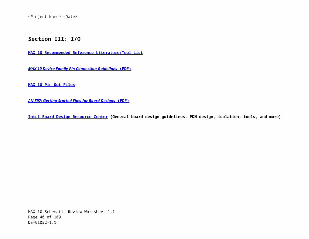
MAX 10 Recommended Reference Literature/Tool List
MAX 10 Device Family Pin Connection Guidelines (PDF)
MAX 10 Pin-Out Files
AN 597: Getting Started Flow for Board Designs (PDF)
Intel Board Design Resource Center (General board design guidelines, PDN design, isolation, tools, and more)
Index
MAX 10 Schematic Review Worksheet 1.1 Page 25 of 67 DS-01052-1.1
<Project Name> <Date>
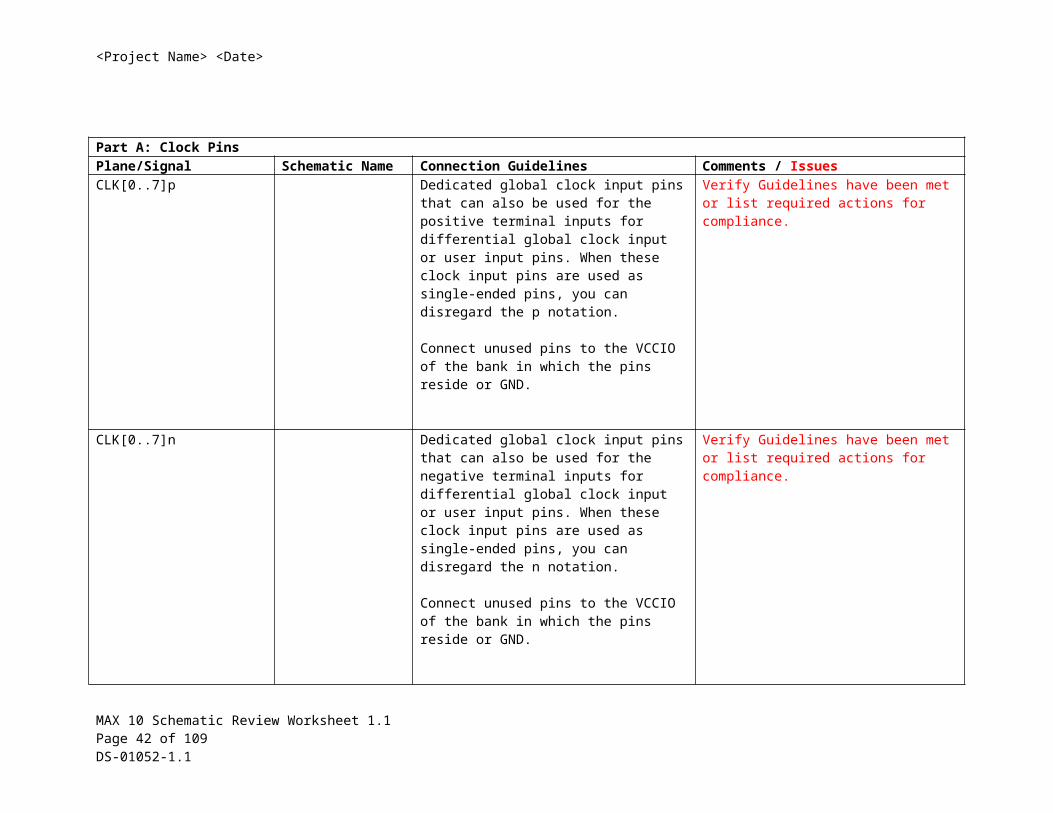
Part A: Clock PinsPlane/Signal Schematic Name Connection Guidelines Comments / IssuesCLK[0..7]p Dedicated global clock input pins that can
also be used for the positive terminal inputs for differential global clock input or user input pins. When these clock input pins are used as single-ended pins, you can disregard the p notation.
Connect unused pins to the VCCIO of the bank in which the pins reside or GND.
Verify Guidelines have been met or list required actions for compliance.
CLK[0..7]n Dedicated global clock input pins that can also be used for the negative terminal inputs for differential global clock input or user input pins. When these clock input pins are used as single-ended pins, you can disregard the n notation.
Connect unused pins to the VCCIO of the bank in which the pins reside or GND.
Verify Guidelines have been met or list required actions for compliance.
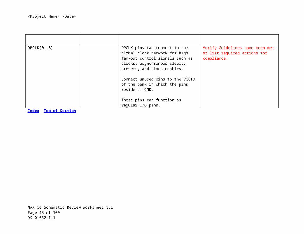
DPCLK[0..3] DPCLK pins can connect to the global clock network for high fan-out control signals such as clocks, asynchronous clears, presets, and clock enables.
Connect unused pins to the VCCIO of the bank in which the pins reside or GND.
These pins can function as regular I/O pins.
Verify Guidelines have been met or list required actions for compliance.
Index Top of Section
MAX 10 Schematic Review Worksheet 1.1 Page 26 of 67 DS-01052-1.1
<Project Name> <Date>
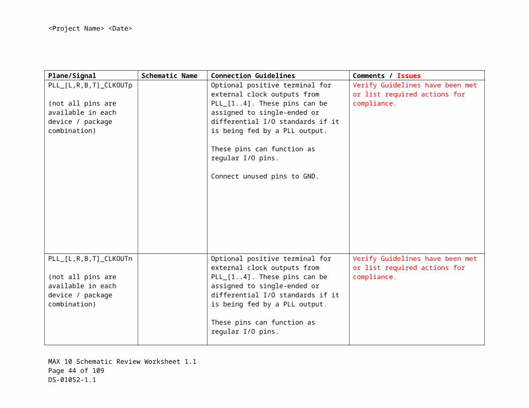
Plane/Signal Schematic Name Connection Guidelines Comments / IssuesPLL_[L,R,B,T]_CLKOUTp
(not all pins are available in each device / package combination)
Optional positive terminal for external clock outputs from PLL_[1..4]. These pins can be assigned to single-ended or differential I/O standards if it is being fed by a PLL output.
These pins can function as regular I/O pins.
Connect unused pins to GND.
Verify Guidelines have been met or list required actions for compliance.
PLL_[L,R,B,T]_CLKOUTn
(not all pins are available in each device / package combination)
Optional positive terminal for external clock outputs from PLL_[1..4]. These pins can be assigned to single-ended or differential I/O standards if it is being fed by a PLL output.
These pins can function as regular I/O pins.
Connect unused pins to GND.
Verify Guidelines have been met or list required actions for compliance.
Index Top of Section
MAX 10 Schematic Review Worksheet 1.1 Page 27 of 67 DS-01052-1.1
<Project Name> <Date>
Additional comments:
Index Top of Section
MAX 10 Schematic Review Worksheet 1.1 Page 28 of 67 DS-01052-1.1
<Project Name> <Date>
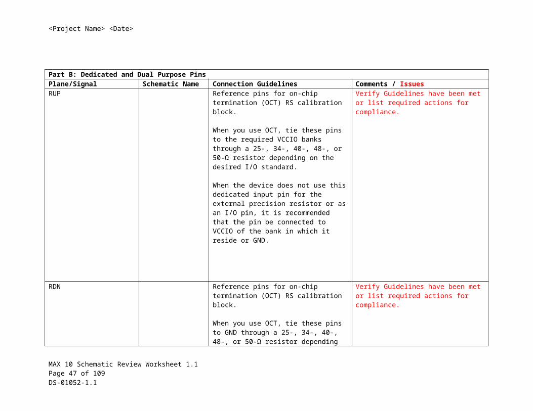
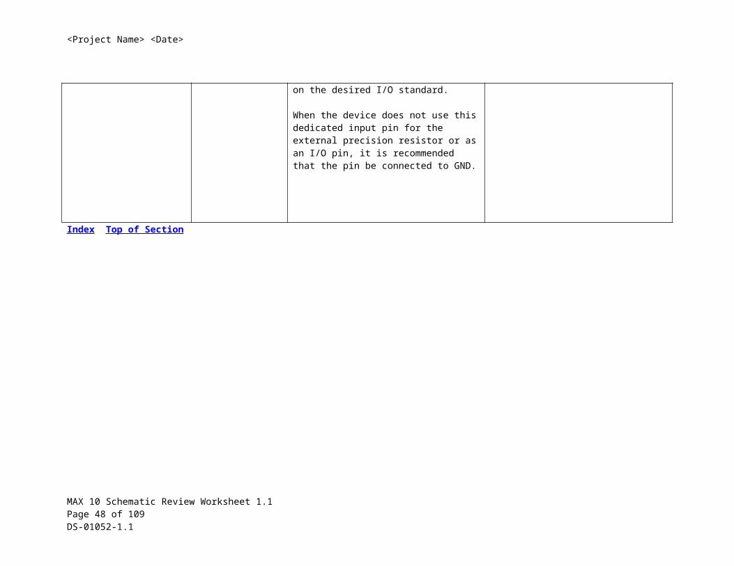
Part B: Dedicated and Dual Purpose PinsPlane/Signal Schematic Name Connection Guidelines Comments / IssuesRUP Reference pins for on-chip termination (OCT)
RS calibration block.
When you use OCT, tie these pins to the required VCCIO banks through a 25-, 34-, 40-, 48-, or 50-Ω resistor depending on the desired I/O standard.
When the device does not use this dedicated input pin for the external precision resistor or as an I/O pin, it is recommended that the pin be connected to VCCIO of the bank in which it reside or GND.
Verify Guidelines have been met or list required actions for compliance.
RDN Reference pins for on-chip termination (OCT) RS calibration block.
When you use OCT, tie these pins to GND through a 25-, 34-, 40-, 48-, or 50-Ω resistor depending on the desired I/O standard.
When the device does not use this dedicated input pin for the external precision resistor or as an I/O pin, it is recommended that the pin be connected to GND.
Verify Guidelines have been met or list required actions for compliance.
Index Top of Section
MAX 10 Schematic Review Worksheet 1.1 Page 29 of 67 DS-01052-1.1
<Project Name> <Date>
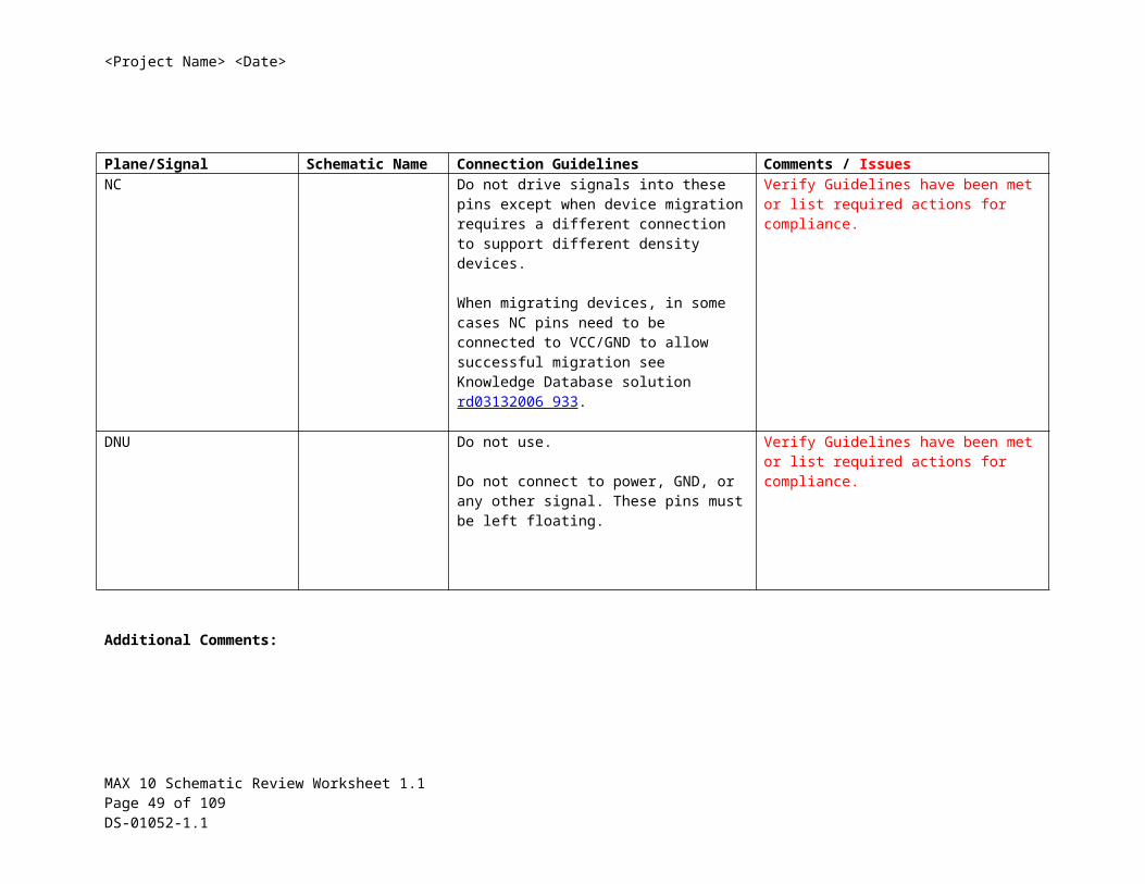
Plane/Signal Schematic Name Connection Guidelines Comments / IssuesNC Do not drive signals into these pins except
when device migration requires a different connection to support different density devices.
When migrating devices, in some cases NC pins need to be connected to VCC/GND to allow successful migration see Knowledge Database solution rd03132006_933.
Verify Guidelines have been met or list required actions for compliance.
DNU Do not use.
Do not connect to power, GND, or any other signal. These pins must be left floating.
Verify Guidelines have been met or list required actions for compliance.
Additional Comments:
Index Top of Section
MAX 10 Schematic Review Worksheet 1.1 Page 30 of 67 DS-01052-1.1
<Project Name> <Date>
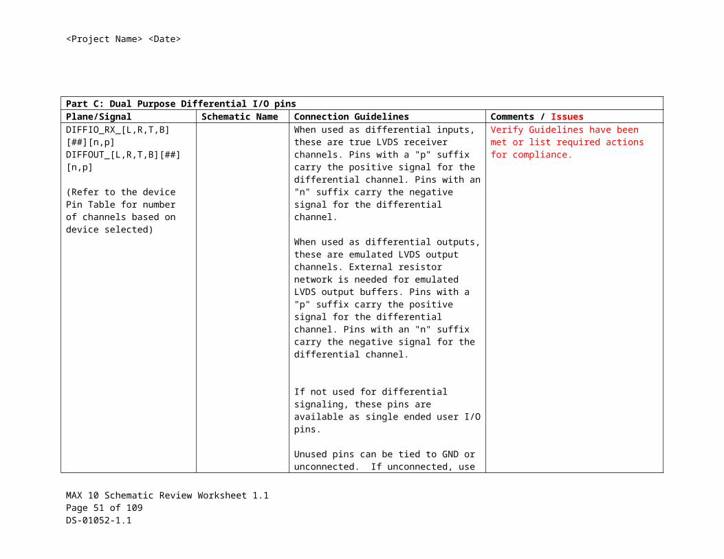
Part C: Dual Purpose Differential I/O pinsPlane/Signal Schematic Name Connection Guidelines Comments / IssuesDIFFIO_RX_[L,R,T,B][##][n,p]DIFFOUT_[L,R,T,B][##][n,p]
(Refer to the device Pin Table for number of channels based on device selected)
When used as differential inputs, these are true LVDS receiver channels. Pins with a "p" suffix carry the positive signal for the differential channel. Pins with an "n" suffix carry the negative signal for the differential channel.
When used as differential outputs, these are emulated LVDS output channels. External resistor network is needed for emulated LVDS output buffers. Pins with a "p" suffix carry the positive signal for the differential channel. Pins with an "n" suffix carry the negative signal for the differential channel.
If not used for differential signaling, these pins are available as single ended user I/O pins.
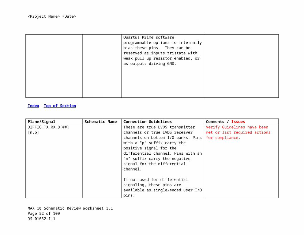
Unused pins can be tied to GND or unconnected. If unconnected, use Quartus Prime software programmable options to internally bias these pins. They can be reserved as inputs tristate with weak pull up resistor enabled, or as outputs driving GND.
Verify Guidelines have been met or list required actions for compliance.
Index Top of Section
MAX 10 Schematic Review Worksheet 1.1 Page 31 of 67 DS-01052-1.1
<Project Name> <Date>
Plane/Signal Schematic Name Connection Guidelines Comments / IssuesDIFFIO_TX_RX_B[##][n,p] These are true LVDS transmitter channels or
true LVDS receiver channels on bottom I/O banks. Pins with a "p" suffix carry the positive signal for the differential channel. Pins with an "n" suffix carry the negative signal for the differential channel.
If not used for differential signaling, these pins are available as single-ended user I/O pins.
Verify Guidelines have been met or list required actions for compliance.
Index Top of Section
MAX 10 Schematic Review Worksheet 1.1 Page 32 of 67 DS-01052-1.1
<Project Name> <Date>
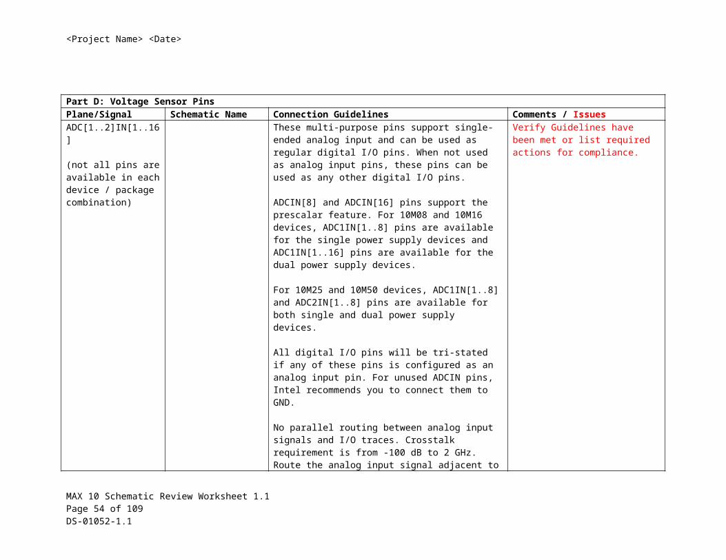
Part D: Voltage Sensor PinsPlane/Signal Schematic Name Connection Guidelines Comments / IssuesADC[1..2]IN[1..16]
(not all pins are available in each device / package combination)
These multi-purpose pins support single-ended analog input and can be used as regular digital I/O pins. When not used as analog input pins, these pins can be used as any other digital I/O pins.
ADCIN[8] and ADCIN[16] pins support the prescalar feature. For 10M08 and 10M16 devices, ADC1IN[1..8] pins are available for the single power supply devices and ADC1IN[1..16] pins are available for the dual power supply devices.
For 10M25 and 10M50 devices, ADC1IN[1..8] and ADC2IN[1..8] pins are available for both single and dual power supply devices.
All digital I/O pins will be tri-stated if any of these pins is configured as an analog input pin. For unused ADCIN pins, Intel recommends you to connect them to GND.
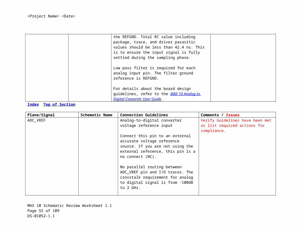
No parallel routing between analog input signals and I/O traces. Crosstalk requirement is from -100 dB to 2 GHz. Route the analog input signal adjacent to the REFGND. Total RC value including package, trace, and driver parasitic values should be less than 42.4 ns. This is to ensure the input signal is fully settled during the sampling phase.
Low pass filter is required for each analog input pin. The filter ground reference is REFGND.
For details about the board design guidelines, refer to the MAX 10 Analog to Digital Converter User Guide.
Verify Guidelines have been met or list required actions for compliance.
Index Top of Section
MAX 10 Schematic Review Worksheet 1.1 Page 33 of 67 DS-01052-1.1
<Project Name> <Date>
Plane/Signal Schematic Name Connection Guidelines Comments / IssuesADC_VREF Analog-to-digital converter voltage reference
input
Connect this pin to an external accurate voltage reference source. If you are not using the external reference, this pin is a no connect (NC).
No parallel routing between ADC_VREF pin and I/O traces. The crosstalk requirement for analog to digital signal is from -100dB to 2 GHz.
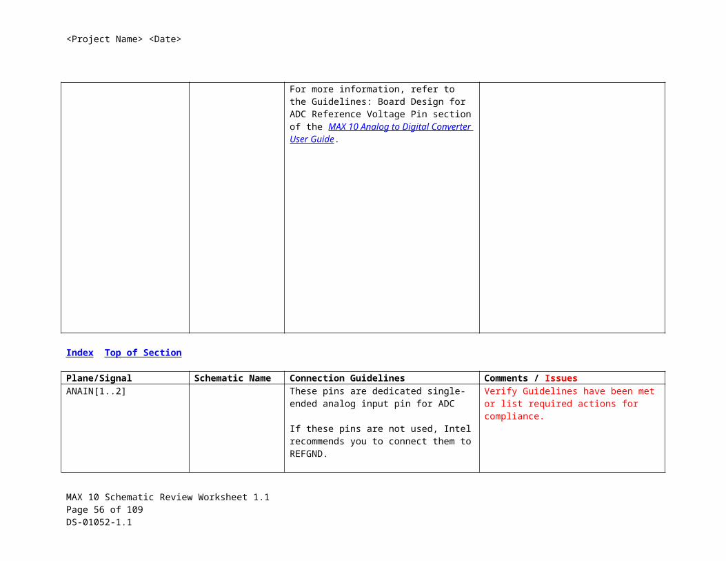
For more information, refer to the Guidelines: Board Design for ADC Reference Voltage Pin section of the MAX 10 Analog to Digital Converter User Guide.
Verify Guidelines have been met or list required actions for compliance.
Index Top of Section
Plane/Signal Schematic Name Connection Guidelines Comments / Issues
MAX 10 Schematic Review Worksheet 1.1 Page 34 of 67 DS-01052-1.1
<Project Name> <Date>
ANAIN[1..2] These pins are dedicated single-ended analog input pin for ADC
If these pins are not used, Intel recommends you to connect them to REFGND.
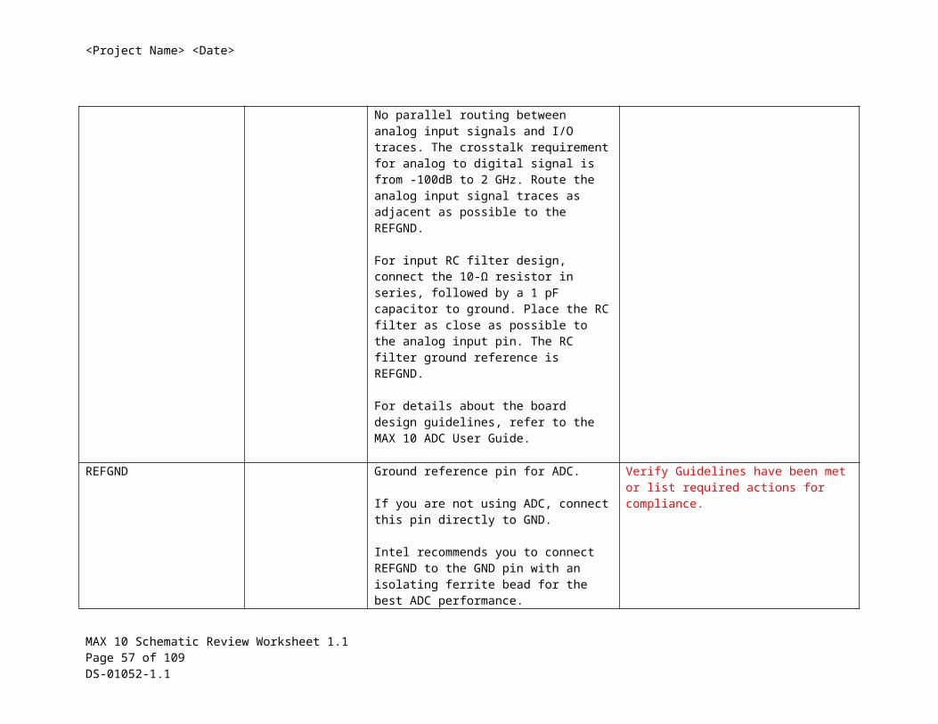
No parallel routing between analog input signals and I/O traces. The crosstalk requirement for analog to digital signal is from -100dB to 2 GHz. Route the analog input signal traces as adjacent as possible to the REFGND.
For input RC filter design, connect the 10-Ω resistor in series, followed by a 1 pF capacitor to ground. Place the RC filter as close as possible to the analog input pin. The RC filter ground reference is REFGND.
For details about the board design guidelines, refer to the MAX 10 ADC User Guide.
Verify Guidelines have been met or list required actions for compliance.
REFGND Ground reference pin for ADC.
If you are not using ADC, connect this pin directly to GND.
Intel recommends you to connect REFGND to the GND pin with an isolating ferrite bead for the best ADC performance.
Verify Guidelines have been met or list required actions for compliance.
Index Top of Section
Additional Comments:
MAX 10 Schematic Review Worksheet 1.1 Page 35 of 67 DS-01052-1.1
<Project Name> <Date>
Index Top of Section
MAX 10 Schematic Review Worksheet 1.1 Page 36 of 67 DS-01052-1.1
<Project Name> <Date>
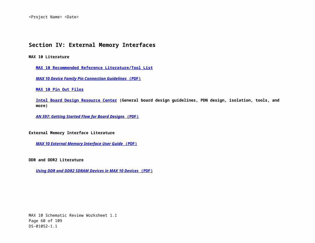
Section IV: External Memory InterfacesMAX 10 Literature
MAX 10 Recommended Reference Literature/Tool List
MAX 10 Device Family Pin Connection Guidelines (PDF)
MAX 10 Pin Out Files
Intel Board Design Resource Center (General board design guidelines, PDN design, isolation, tools, and more)
AN 597: Getting Started Flow for Board Designs (PDF)
External Memory Interface Literature
MAX 10 External Memory Interface User Guide (PDF)
DDR and DDR2 Literature
Using DDR and DDR2 SDRAM Devices in MAX 10 Devices (PDF)
Index
MAX 10 Schematic Review Worksheet 1.1 Page 37 of 67 DS-01052-1.1
<Project Name> <Date>
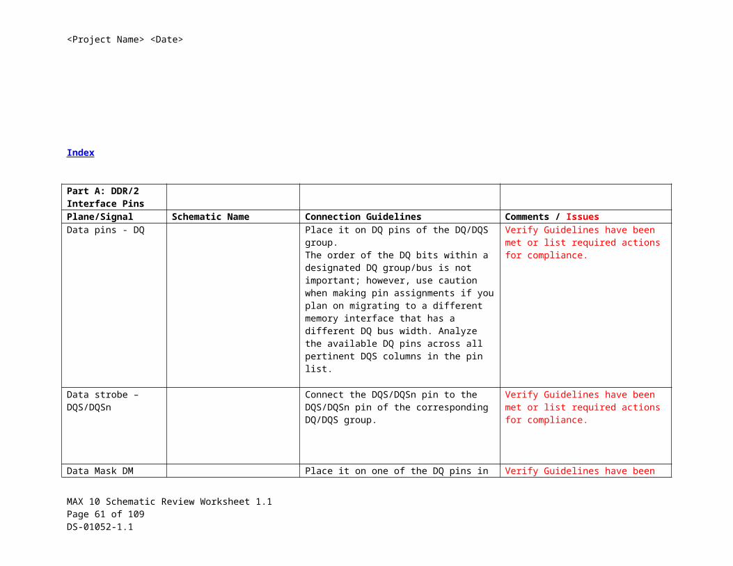
Part A: DDR/2 Interface PinsPlane/Signal Schematic Name Connection Guidelines Comments / IssuesData pins - DQ Place it on DQ pins of the DQ/DQS group.
The order of the DQ bits within a designated DQ group/bus is not important; however, use caution when making pin assignments if you plan on migrating to a different memory interface that has a different DQ bus width. Analyze the available DQ pins across all pertinent DQS columns in the pin list.
Verify Guidelines have been met or list required actions for compliance.
Data strobe – DQS/DQSn
Connect the DQS/DQSn pin to the DQS/DQSn pin of the corresponding DQ/DQS group.
Verify Guidelines have been met or list required actions for compliance.
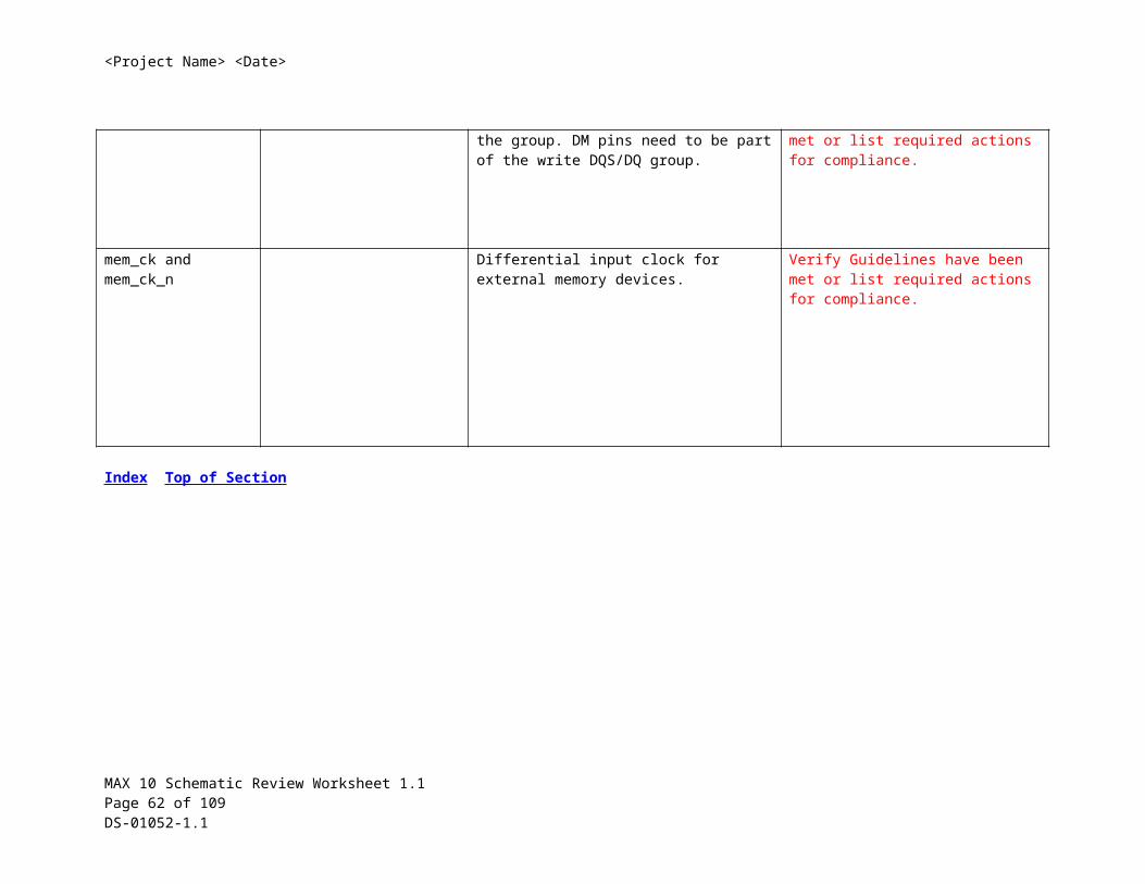
Data Mask DM Place it on one of the DQ pins in the group. DM pins need to be part of the write DQS/DQ group.
Verify Guidelines have been met or list required actions for compliance.
mem_ck andmem_ck_n
Differential input clock for external memory devices.
Verify Guidelines have been met or list required actions for compliance.
Index Top of Section
MAX 10 Schematic Review Worksheet 1.1 Page 38 of 67 DS-01052-1.1
<Project Name> <Date>
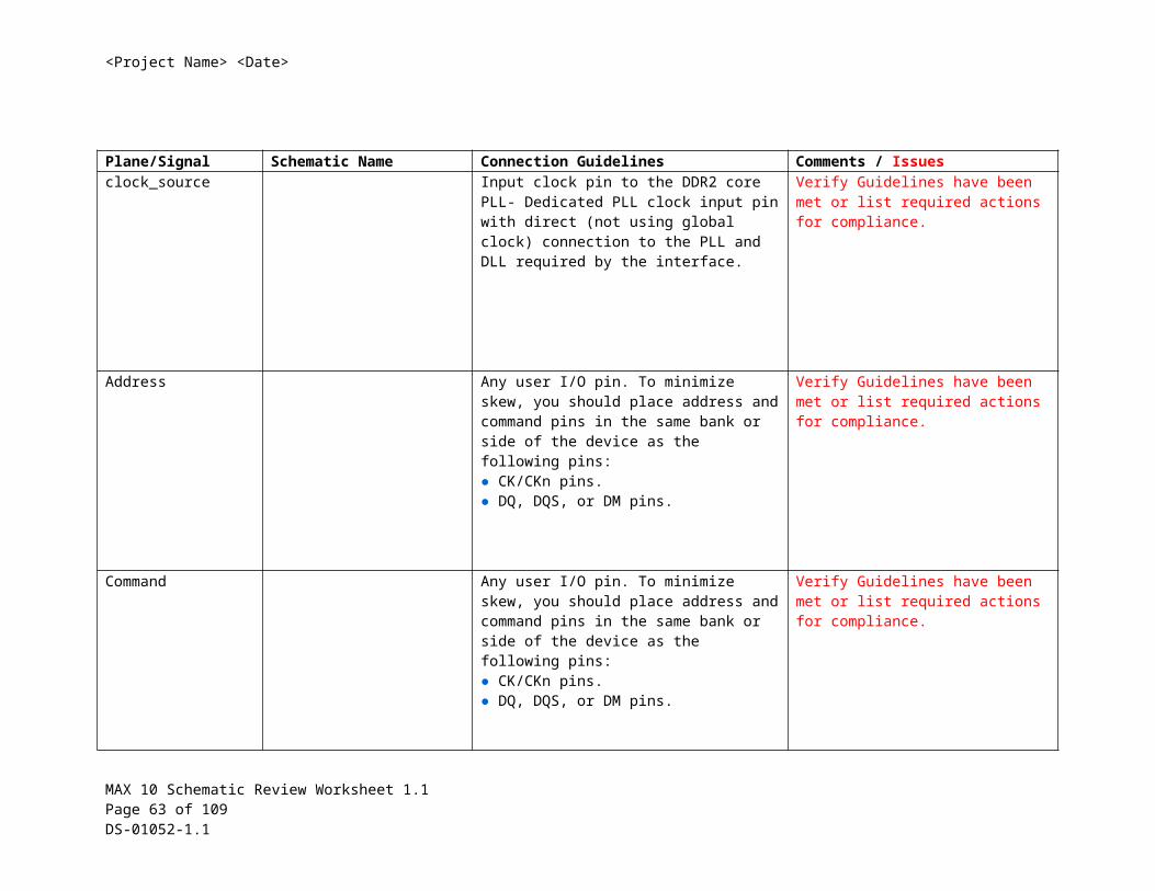
Plane/Signal Schematic Name Connection Guidelines Comments / Issuesclock_source Input clock pin to the DDR2 core PLL-
Dedicated PLL clock input pin with direct (not using global clock) connection to the PLL and DLL required by the interface.
Verify Guidelines have been met or list required actions for compliance.
Address Any user I/O pin. To minimize skew, you should place address and command pins in the same bank or side of the device as the following pins:● CK/CKn pins.● DQ, DQS, or DM pins.
Verify Guidelines have been met or list required actions for compliance.
Command Any user I/O pin. To minimize skew, you should place address and command pins in the same bank or side of the device as the following pins:● CK/CKn pins.● DQ, DQS, or DM pins.
Verify Guidelines have been met or list required actions for compliance.
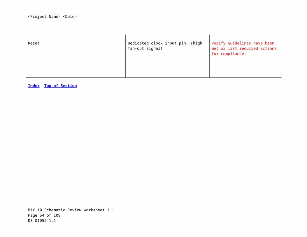
Reset Dedicated clock input pin. (high fan-out signal) Verify Guidelines have been met or list required actions for compliance.
Index Top of Section
MAX 10 Schematic Review Worksheet 1.1 Page 39 of 67 DS-01052-1.1
<Project Name> <Date>
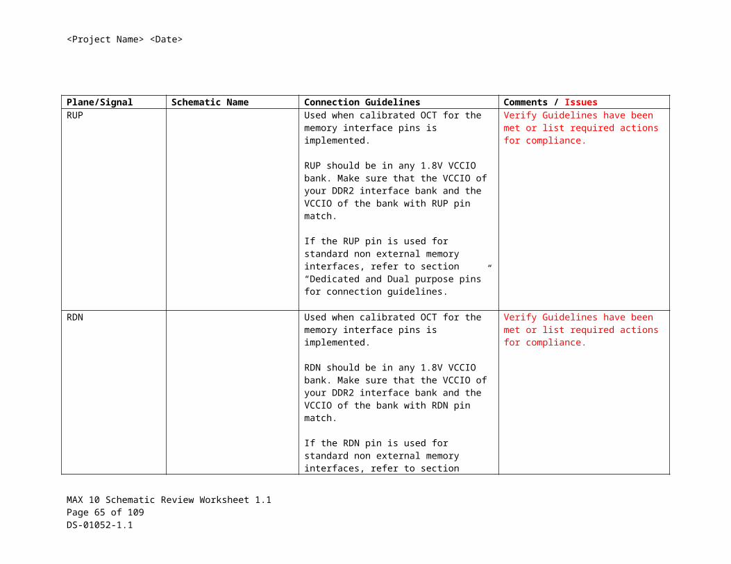
Plane/Signal Schematic Name Connection Guidelines Comments / IssuesRUP Used when calibrated OCT for the memory
interface pins is implemented.
RUP should be in any 1.8V VCCIO bank. Make sure that the VCCIO of your DDR2 interface bank and the VCCIO of the bank with RUP pin match.
If the RUP pin is used for standard non external memory interfaces, refer to section “Dedicated and Dual purpose pins” for connection guidelines.
Verify Guidelines have been met or list required actions for compliance.
RDN Used when calibrated OCT for the memory interface pins is implemented.
RDN should be in any 1.8V VCCIO bank. Make sure that the VCCIO of your DDR2 interface bank and the VCCIO of the bank with RDN pin match.
If the RDN pin is used for standard non external memory interfaces, refer to section “Dedicated and Dual purpose pins” for connection guidelines.
Verify Guidelines have been met or list required actions for compliance.
Additional Comments:
Index Top of Section
MAX 10 Schematic Review Worksheet 1.1 Page 40 of 67 DS-01052-1.1
<Project Name> <Date>
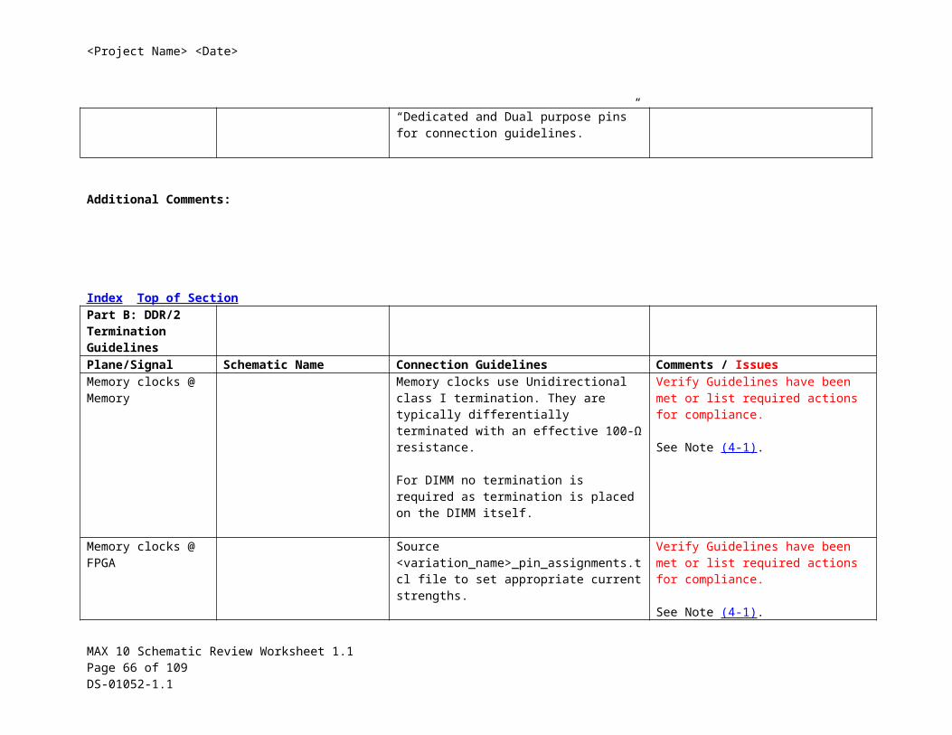
Part B: DDR/2 Termination GuidelinesPlane/Signal Schematic Name Connection Guidelines Comments / IssuesMemory clocks @ Memory
Memory clocks use Unidirectional class I termination. They are typically differentially terminated with an effective 100-Ω resistance.
For DIMM no termination is required as termination is placed on the DIMM itself.
Verify Guidelines have been met or list required actions for compliance.
See Note (4-1).
Memory clocks @ FPGA
Source <variation_name>_pin_assignments.tcl file to set appropriate current strengths.
Verify Guidelines have been met or list required actions for compliance.
See Note (4-1).
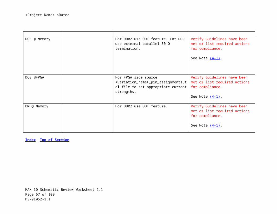
DQS @ Memory For DDR2 use ODT feature. For DDR use external parallel 50-Ω termination.
Verify Guidelines have been met or list required actions for compliance.
See Note (4-1).
DQS @FPGA For FPGA side source <variation_name>_pin_assignments.tcl file to set appropriate current strengths.
Verify Guidelines have been met or list required actions for compliance.
See Note (4-1).
DM @ Memory For DDR2 use ODT feature. Verify Guidelines have been met or list required actions for compliance.
See Note (4-1).
Index Top of Section
MAX 10 Schematic Review Worksheet 1.1 Page 41 of 67 DS-01052-1.1
<Project Name> <Date>
Plane/Signal Schematic Name Connection Guidelines Comments / IssuesDQ @FPGA For FPGA side source
<variation_name>_pin_assignments.tcl file to set appropriate current strengths.
Verify Guidelines have been met or list required actions for compliance.
See Note (4-1).
DQ @ Memory For DDR2 use ODT feature. . For DDR use external parallel 50-Ω termination.
Verify Guidelines have been met or list required actions for compliance.
See Note (4-1).
DM @ FPGA For FPGA side source <variation_name>_pin_assignments.tcl file to set appropriate current strengths.
Verify Guidelines have been met or list required actions for compliance.
See Note (4-1).
Address [BA, mem_addr] @ Memory
Unidirectional class I termination. For multi-loads Intel recommends the ideal topology is a balanced symmetrical tree. Intel recommends that the class I termination to VTT is placed:■ At the first split or division of the symmetrical tree for discrete devices. Nonsymmetrical topologies result in over or undershoot and oscillations on the line, which may require compensation capacitors or a lower than ideal drive strength to be specified resulting in de-rated interface performance.
Verify Guidelines have been met or list required actions for compliance.
See Note (4-1).
Index Top of Section
MAX 10 Schematic Review Worksheet 1.1 Page 42 of 67 DS-01052-1.1
<Project Name> <Date>
Plane/Signal Schematic Name Connection Guidelines Comments / IssuesAddress [BA, mem_addr] @ FPGA
For FPGA side source <variation_name>_pin_assignments.tcl file to set appropriate current strengths.
Verify Guidelines have been met or list required actions for compliance.
See Note (4-1).
Command [CKE, CS_N, RAS, CAS, WE_N] @ Memory
Unidirectional class I termination. For multi-loads Intel recommends the ideal topology is a balanced symmetrical tree. Intel recommends that the class I termination to VTT is placed:■ At the first split or division of the symmetrical tree for discrete devices. Nonsymmetrical topologies result in over or undershoot and oscillations on the line, which may require compensation capacitors or a lower than ideal drive strength to be specified resulting in de-rated interface performance.
Verify Guidelines have been met or list required actions for compliance.
See Note (4-1).
Command [CKE, CS_N, RAS, CAS, WE_N] @ FPGA
For FPGA side source <variation_name>_pin_assignments.tcl file to set appropriate current strengths.
Verify Guidelines have been met or list required actions for compliance.
See Note (4-1).
Notes:4-1. The termination schemes suggested in the table are general guidelines. You should do board level simulation for your particular system/board to determine optimal termination scheme.
Index Top of Section
MAX 10 Schematic Review Worksheet 1.1 Page 43 of 67 DS-01052-1.1
<Project Name> <Date>
Miscellaneous
Pin Description Schematic Name Connection Guidelines Comments/ IssuesVref Use a voltage regulator to generate this
voltage.Verify Guidelines have been met or list required actions for compliance.
See Note (4-2).Vtt Use a voltage regulator to generate this
voltage.Verify Guidelines have been met or list required actions for compliance.
See Note (4-2).RUP & RDN RUP pin is connected to VCCIO (1.8V)
through an external 50-Ω ±1% resistor.
RDN pin is connected to GND through a 50-Ω ±1% resistor.
If the RUP and RDN pins are used for standard non external memory interfaces, refer to section “Dedicated and Dual purpose pins” for connection guidelines.
Verify Guidelines have been met or list required actions for compliance.
Notes:
4-2. This worksheet does not calculate required decoupling, it is expected the designer will select decoupling based on analysis of power required and impedance of power path required based on static and switching current values. Refer to Intel’s Power Delivery Network (PDN) Tool for further information.
Capacitance values for the power supply should be selected after consideration of the amount of power they need to supply over the frequency of operation of the particular circuit being decoupled. A target impedance for the power plane should be calculated based on current draw and voltage drop requirements of the device/supply. The power plane should then be decoupled using the appropriate number of capacitors. On-board capacitors do not decouple higher than 100 MHz due to “Equivalent Series Inductance” of the mounting of the packages. Proper board design techniques such as interplane capacitance with low inductance should be considered for higher frequency decoupling.
Index Top of SectionAdditional Comments:
MAX 10 Schematic Review Worksheet 1.1 Page 44 of 67 DS-01052-1.1
<Project Name> <Date>
Index Top of Section
Part C: DDR3
MAX 10 Schematic Review Worksheet 1.1 Page 45 of 67 DS-01052-1.1
<Project Name> <Date>
Interface PinsPlane/Signal Schematic Name Connection Guidelines Comments / IssuesData pin - DQ Place it on DQ pins of the DQ/DQS group.
The order of the DQ bits within a designated DQ group/bus is not important; however, use caution when making pin assignments if you plan on migrating to a different memory interface that has a different DQ bus width (e.g. migrating from x4 to x8). Analyze the available DQ pins across all pertinent DQS columns in the pin list.
Verify Guidelines have been met or list required actions for compliance.
See Note (5-3).
Data strobe - DQS/DQSn
Should be placed on corresponding DQS and DQSn pins of the DQ/DQS group.
Verify Guidelines have been met or list required actions for compliance.
See Notes (5-3) (5-4).
Index Top of Section
Plane/Signal Schematic Name Connection Guidelines Comments / Issuesmem_ck and Place on any unused DQ or DQS pins with Verify Guidelines have been met or list
MAX 10 Schematic Review Worksheet 1.1 Page 46 of 67 DS-01052-1.1
<Project Name> <Date>
mem_ck_n DIFFOUT capability for the mem_clk[n:0] and mem_clk_n[n:0] signals (where n>=0).
Do not place CK and CK# pins in the samegroup as any other DQ or DQS pins.
If there are multiple CK and CK# pin pairs, place them on DIFFOUT in the same single DQ group of adequate width.
required actions for compliance.
See Note (5-3).
Index Top of Section
Plane/Signal Schematic Name Connection Guidelines Comments / Issuesclock_source Input clock pin to the DDR3 core PLL - Verify Guidelines have been met or list
MAX 10 Schematic Review Worksheet 1.1 Page 47 of 67 DS-01052-1.1
<Project Name> <Date>
Dedicated PLL clock input pin with direct (not using a global clock net) connection to the PLL and DLL required by the interface.
required actions for compliance.
DM Data Mask Pin – Place it on one of the DQ pins in the group. DM pins need to be part of the DQS/DQ group.
Verify Guidelines have been met or list required actions for compliance.
See Note (5-4).
Address Any user I/O pin. To minimize skew, you should place address and command pins in the same bank or side of the device as the following pins:● mem_clk* pins.● DQ, DQS, or DM pins.
Verify Guidelines have been met or list required actions for compliance.
See Note (5-4).
Command Any user I/O pin. To minimize skew, you should place address and command pins in the same bank or side of the device as the following pins:● mem_clk* pins.● DQ, DQS, or DM pins.
Verify Guidelines have been met or list required actions for compliance.
See Note (5-4).
Index Top of Section
MAX 10 Schematic Review Worksheet 1.1 Page 48 of 67 DS-01052-1.1
<Project Name> <Date>
Plane/Signal Schematic Name Connection Guidelines Comments / IssuesReset for DDR3 Memory
Any user I/O pin in the same bank or side of the device as the following pins:● mem_clk* pins.● DQ, DQS, or DM pins.
Verify Guidelines have been met or list required actions for compliance.
Reset Dedicated clock input pin. (high fan-out signal)The reset pin can alternatively be generated.
Ensure the DDR3 IP closes reset Recovery/Removal timing in Report DDR.
Verify Guidelines have been met or list required actions for compliance.
Index Top of Section
MAX 10 Schematic Review Worksheet 1.1 Page 49 of 67 DS-01052-1.1

<Project Name> <Date>
Plane/Signal Schematic Name Connection Guidelines Comments / IssuesRUP Used when calibrated OCT for the memory
interface pins is implemented.
RUP should be in any 1.5V VCCIO bank. Make sure that the VCCIO of your DDR3 interface bank and the VCCIO of the bank with RUP pin match.
If the RUP pin is used for standard non external memory interfaces, refer to section “Dedicated and Dual purpose pins” for connection guidelines.
Verify Guidelines have been met or list required actions for compliance.
RDN Used when calibrated OCT for the memory interface pins is implemented.
RDN should be in any 1.5V VCCIO bank. Make sure that the VCCIO of your DDR3 interface bank and the VCCIO of the bank with RDN pin match.
If the RDN pin is used for standard non external memory interfaces, refer to section “Dedicated and Dual purpose pins” for connection guidelines.
Verify Guidelines have been met or list required actions for compliance.
Additional Comments:
Index Top of Section
MAX 10 Schematic Review Worksheet 1.1 Page 50 of 67 DS-01052-1.1
<Project Name> <Date>
Notes:
5-3. DDR3 only supports differential DQS signaling.
Additional Comments:
Index Top of SectionPart D: DDR3
MAX 10 Schematic Review Worksheet 1.1 Page 51 of 67 DS-01052-1.1
<Project Name> <Date>
Interface Termination GuidelinesPlane/Signal Schematic Name Connection Guidelines Comments / IssuesMemory clocks@ Memory
Max 10 V devices do not support DDR3 SDRAM with read or write leveling, so these devices do not support standard DDR3 SDRAM DIMMs or DDR3 SDRAM components using the standard DDR3 SDRAM fly-by address, command, and clock layout topology.
Devices (without leveling) – differential termination resistor needs to be included in the design. Depending on your board stackup and layout requirements, you choose your differential termination resistor value.
Verify Guidelines have been met or list required actions for compliance.
See Note (5-5).
Memory clocks@ FPGA
Use series 50-Ω output termination without calibration.
Source <variation_name>_pin_assignments.tcl to make the setting.
Verify Guidelines have been met or list required actions for compliance.
See Note (5-5).
DQS @ Memory Use ODT. Verify Guidelines have been met or list required actions for compliance.
See Note (5-5).
Index Top of Section
MAX 10 Schematic Review Worksheet 1.1 Page 52 of 67 DS-01052-1.1
<Project Name> <Date>
Plane/Signal Schematic Name Connection Guidelines Comments / IssuesDQS @ FPGA Use parallel 50-Ω with calibration as input
termination and Use series 50-Ω with calibration as output termination.Source <variation_name>_pin_assignments.tcl file to make these assignments automatically.
Verify Guidelines have been met or list required actions for compliance.
See Note (5-5).
DQ @ Memory Use ODT. Verify Guidelines have been met or list required actions for compliance.
See Note (5-5).
DQ @ FPGA Use parallel 50-Ω with calibration as input termination and Use series 50-Ω with calibration as output termination.Source <variation_name>_pin_assignments.tcl file to assign these assignments automatically.
Verify Guidelines have been met or list required actions for compliance.
See Note (5-5).
DM@ Memory Use ODT. Verify Guidelines have been met or list required actions for compliance.
See Note (5-5).
DM @ FPGA Use series 50-Ω with calibration as output termination. Source <variation_name>_pin_assignments.tcl file to make this assignment automatically.
Verify Guidelines have been met or list required actions for compliance.
See Note (5-5).
Index Top of Section
MAX 10 Schematic Review Worksheet 1.1 Page 53 of 67 DS-01052-1.1
<Project Name> <Date>
Plane/Signal Schematic Name Connection Guidelines Comments / IssuesAddress [BA, mem_addr] @ Memory
Discrete Device (no leveling) - Unidirectional class I termination.
Unidirectional class I termination. For multi-loads Intel recommends the ideal topology is a balanced symmetrical tree. Intel recommends that the class I termination to VTT is placed at the first split or division of the symmetrical tree for discrete devices.
Verify Guidelines have been met or list required actions for compliance.
See Note (5-5).
Address [BA, mem_addr] @ FPGA
Use maximum current drive strength. Source <variation_name>_pin_assignments.tcl file to make this assignment automatically.
Verify Guidelines have been met or list required actions for compliance.
See Note (5-5).
Command [CKE, CS_N, ODT, RAS, CAS, WE_N] @ Memory
Discrete Device (no leveling) - Unidirectional class I termination.
Unidirectional class I termination. For multi-loads Intel recommends the ideal topology is a balanced symmetrical tree. Intel recommends that the class I termination to VTT is placed at the first split or division of the symmetrical tree for discrete devices.
Verify Guidelines have been met or list required actions for compliance.
See Note (5-5).
Index Top of Section
MAX 10 Schematic Review Worksheet 1.1 Page 54 of 67 DS-01052-1.1
<Project Name> <Date>
Plane/Signal Schematic Name Connection Guidelines Comments / IssuesCommand [CKE, CS_N, ODT, RAS, CAS, WE_N] @ FPGA
Use maximum current drive strength. Source <variation_name>_pin_assignments.tcl file to make this assignment automatically.
Verify Guidelines have been met or list required actions for compliance.
See Note (5-5).
Reset for DDR3 Memory
Use 1.5V CMOS output.
It is not recommended to terminate this reset to Vtt.
Verify Guidelines have been met or list required actions for compliance.
Notes:
5-5. The termination schemes suggested in the table are general guidelines. You should do board level simulation for your particular system/board to determine optimal termination scheme.
Additional Comments:
Index Top of Section
MAX 10 Schematic Review Worksheet 1.1 Page 55 of 67 DS-01052-1.1
<Project Name> <Date>
MiscellaneousPin Description Schematic Name Connection Guidelines Comments / IssuesVref Use a voltage regulator to generate this
voltage.Verify Guidelines have been met or list required actions for compliance.
Vtt Use a voltage regulator to generate this voltage.
Typically DDR3 DIMMS have decoupling capacitors connected between VTT and VDD (1.5V) and it is recommended that designers follow this approach.
Note that DDR3 DIMM layout topology is not supported.
Verify Guidelines have been met or list required actions for compliance.
RUP & RDN RUP pin is connected to VCCIO (1.5V) through an external 50-Ω ±1% resistor.
RDN pin is connected to GND through a 50-Ω ±1% resistor.
If the RUP and RDN pins are used for standard non external memory interfaces, refer to section “Dedicated and Dual purpose pins” for connection guidelines.
Verify Guidelines have been met or list required actions for compliance.
Additional Comments:
Index Top of Section
MAX 10 Schematic Review Worksheet 1.1 Page 56 of 67 DS-01052-1.1
<Project Name> <Date>
Part E: LPDDR2 Interface PinsPlane/Signal Schematic Name Connection Guidelines Comments / IssuesData pins - DQ Place it on DQ pins of the DQ/DQS group.
The order of the DQ bits within a designated DQ group/bus is not important.
Verify Guidelines have been met or list required actions for compliance.
See Note (5-6).
Data strobe - DQS/DQSn
Differential DQS - Should be placed on corresponding DQS and DQSn pins of the DQ/DQS group.
Verify Guidelines have been met or list required actions for compliance.
See Note (5-6).
Data Mask DM Place it on one of the DQ pins in the group. DM pins need to be part of the write DQ/DQS group.
Verify Guidelines have been met or list required actions for compliance.
See Note (5-6).
Index Top of Section
MAX 10 Schematic Review Worksheet 1.1 Page 57 of 67 DS-01052-1.1
<Project Name> <Date>
Plane/Signal Schematic Name Connection Guidelines Comments / Issuesmem_ck and mem_ck_n
Place on any unused DQ or DQS pins with DIFFOUT capability for the mem_clk[n:0] and mem_clk_n[n:0] signals (where n>=0).
Do not place CK and CK# pins in the samegroup as any other DQ or DQS pins.
If there are multiple CK and CK# pin pairs, place them on DIFFOUT in the same single DQ group of adequate width.
Verify Guidelines have been met or list required actions for compliance.
See Note (5-6).
Index Top of Section
MAX 10 Schematic Review Worksheet 1.1 Page 58 of 67 DS-01052-1.1
<Project Name> <Date>
Plane/Signal Schematic Name Connection Guidelines Comments / Issuesclock_source Input clock pin to the LPDDR2 core PLL -
Dedicated PLL clock input pin with direct (not using a global clock net) connection to the PLL and DLL required by the interface.
Verify Guidelines have been met or list required actions for compliance.
Address/Command The LPDDR2 command code includes the address, cs_n and cke signals. Any DDR-capable I/O pin. DDR capable pins include pins that are in a DQ/DQS group andthe 4 additional pins that make up the 16-pin group. Refer to the device pin tables for further information. To minimize skew, you should place address and command pins in the same bank or side of the device as the following pins:● CK/CK#● DQ. DQS, or DM pins.
Verify Guidelines have been met or list required actions for compliance.
See Note (5-6).
Index Top of Section
MAX 10 Schematic Review Worksheet 1.1 Page 59 of 67 DS-01052-1.1
<Project Name> <Date>
Plane/Signal Schematic Name Connection Guidelines Comments / IssuesReset Dedicated clock input pin. (high fan-out signal)
The reset pin can alternatively be generated.
Ensure the LPDDR2 IP closes reset Recovery/Removal timing in Report DDR.
Verify Guidelines have been met or list required actions for compliance.
RUP Used when calibrated OCT for the memory interface pins is implemented.
RUP should be in any 1.5V VCCIO bank. Make sure that the VCCIO of your DDR3 interface bank and the VCCIO of the bank with RUP pin match.
If the RUP pin is used for standard non external memory interfaces, refer to section “Dedicated and Dual purpose pins” for connection guidelines.
Verify Guidelines have been met or list required actions for compliance.
RDN Used when calibrated OCT for the memory interface pins is implemented.
RDN should be in any 1.5V VCCIO bank. Make sure that the VCCIO of your DDR3 interface bank and the VCCIO of the bank with RDN pin match.
If the RDN pin is used for standard non external memory interfaces, refer to section “Dedicated and Dual purpose pins” for connection guidelines.
Verify Guidelines have been met or list required actions for compliance.
Index Top of Section
MAX 10 Schematic Review Worksheet 1.1 Page 60 of 67 DS-01052-1.1
<Project Name> <Date>
Notes:
5-6. Max 10 devices have pre-assigned pins for LPDDR2 SDRAM interfaces.
Additional Comments:
Index Top of Section
MAX 10 Schematic Review Worksheet 1.1 Page 61 of 67 DS-01052-1.1
<Project Name> <Date>
Part F: LPDDR2 Termination GuidelinesPlane/Signal Schematic Name Connection Guidelines Comments / IssuesMemory clocks @ Memory
Memory clocks use Unidirectional class I termination. They are typically differentially terminated with an effective 100-Ω resistance.
Verify Guidelines have been met or list required actions for compliance.
See Note (5-7).
Memory clocks@ FPGA
Use series 34-Ω output termination without calibration on the FPGA side. Source <variation_name>_pin_assignments.tcl file to make these assignments automatically.
Verify Guidelines have been met or list required actions for compliance.
See Note (5-7).
DQS @ Memory LPDDR2 does not use ODT. Typically an LPDDR2 memory component has a 240 ohm resistor connected between its ZQ pin and GND or VDDCA to allow mode register programming of the driver output impedance. Refer to the LPDDR2 SDRAM data sheet for further information.
Verify Guidelines have been met or list required actions for compliance.
See Note (5-7).
DQS @ FPGA Use series 34-Ω with calibration as output termination. Source <variation_name>_pin_assignments.tcl file to make these assignments automatically.
Verify Guidelines have been met or list required actions for compliance.
See Note (5-7).
Index Top of Section
MAX 10 Schematic Review Worksheet 1.1 Page 62 of 67 DS-01052-1.1
<Project Name> <Date>
Plane/Signal Schematic Name Connection Guidelines Comments / IssuesDQ @ Memory LPDDR2 does not use ODT. Typically, an
LPDDR2 memory component has a 240 ohm resistor connected between its ZQ pin and GND or VDDCA to allow mode register programming of the driver output impedance. Refer to the LPDDR2 SDRAM data sheet for further information.
Verify Guidelines have been met or list required actions for compliance.
See Note (5-7).
DQ @ FPGA Use series 34-Ω with calibration as output termination. Source<variation_name>_pin_assignments.tcl file to assign these assignments automatically.
Verify Guidelines have been met or list required actions for compliance.
DM@ Memory LPDDR2 does not use ODT. No termination is recommended at the memory component.
Verify Guidelines have been met or list required actions for compliance.
See Note (5-7).
DM @ FPGA Use series 34-Ω with calibration as output termination. Source <variation_name>_pin_assignments.tcl file to make this assignment automatically.
Verify Guidelines have been met or list required actions for compliance.
Index Top of SectionPlane/Signal Schematic Name Connection Guidelines Comments / Issues
MAX 10 Schematic Review Worksheet 1.1 Page 63 of 67 DS-01052-1.1
<Project Name> <Date>
Address/Command [CA, CS_N, CKE] @ Memory
Parallel termination is not recommended to save power.
For multi-loads Intel recommends the ideal topology is a balanced symmetrical tree.
Nonsymmetrical topologies may result in over or undershoot and oscillations on the line, which may require compensation capacitors or a lower than ideal drive strength to be specified resulting in de-rated interface performance.
For CKE, a 4.7K resistor to GND is recommended if your design meets the power sequencing requirements of the LPDDR2 SDRAM component. Refer to the LPDDR2 SDRAM data sheet for further information.
Use maximum current strength as the output drive strength. Source <variation_name>_pin_assignments.tcl file to make this assignment automatically.
Verify Guidelines have been met or list required actions for compliance.
See Note (5-7).
Notes:
5-7. The termination schemes suggested in the table are general guidelines. You should do board level simulation for your particular system/board to determine optimal termination scheme. As many signals are not recommended use parallel terminations at the receiving end of the line to save power, it is strongly recommended to perform board level simulations to verify the signal integrity of your interface.
Index Top of Section
MAX 10 Schematic Review Worksheet 1.1 Page 64 of 67 DS-01052-1.1
<Project Name> <Date>
MiscellaneousPin Description Schematic Name Connection Guidelines Comments/ IssuesVref Use voltage regulator to generate this voltage. Verify Guidelines have been met or list
required actions for compliance.
See Note (5-8).
RUP & RDN RUP pin is connected to VCCIO (1.5V) through an external 50-Ω ±1% resistor.
RDN pin is connected to GND through a 50-Ω ±1% resistor.
If the RUP and RDN pins are used for standard non external memory interfaces, refer to section “Dedicated and Dual purpose pins” for connection guidelines.
Verify Guidelines have been met or list required actions for compliance.
Notes:
5-8. This worksheet does not calculate required decoupling, it is expected the designer will select decoupling based on analysis of power required and impedance of power path required based on static and switching current values. Refer to Intel’s Power Delivery Network (PDN) Tool for Max 10 Devices for further information.
Capacitance values for the power supply should be selected after consideration of the amount of power they need to supply over the frequency of operation of the particular circuit being decoupled. A target impedance for the power plane should be calculated based on current draw and voltage drop requirements of the device/supply. The power plane should then be decoupled using the appropriate number of capacitors. On-board capacitors do not decouple higher than 100 MHz due to “Equivalent Series Inductance” of the mounting of the packages. Proper board design techniques such as interplane capacitance with low inductance should be considered for higher frequency decoupling.
Index Top of Section
MAX 10 Schematic Review Worksheet 1.1 Page 65 of 67 DS-01052-1.1
<Project Name> <Date>
Additional Comments:
Index Top of Section
MAX 10 Schematic Review Worksheet 1.1 Page 66 of 67 DS-01052-1.1
<Project Name> <Date>
Section V: Document Revision HistoryRevision Changes Made Date
V1.1
Rebranded as Intel. Changed instances of Quartus II to Quartus Prime Changed connection guidelines of TCK, TMS, TDI, TDO pins. Add DNU pin. Updated the pin connection guidelines of VCCIO[#] pins. Updated the pin connection guidelines of ADC_VREF pin. Updated the pin connection guidelines of ADC[1..2]IN[1..16] pins. Updated the pin connection guidelines of DPCLK[0..3] pins. Updated the pin connection guidelines of PLL_[L,R,B,T]_CLKOUTp and
PLL_[L,R,B,T]_CLKOUTn pins. Updated the pin connection guidelines of VREFB<#>N0 pins. Updated the pin connection guidelines of VCC_ONE pins. Updated the pin name from BOOT_SEL to CONFIG_SEL. Updated the pin connection guidelines of CONFIG_SEL pin. Updated the pin connection guidelines of CONF_DONE pin. Updated the pin connection guidelines of nSTATUS pin.
Jun 2017
V1.0 Initial Release based on the MAX 10 Pin Connection Guidelines version 1.0. Aug 2014
Index
MAX 10 Schematic Review Worksheet 1.1 Page 67 of 67 DS-01052-1.1