Embed Size (px)
Citation preview
Calhoun: The NPS Institutional Archive
Theses and Dissertations Thesis Collection
2015-09
Maximum power point tracking of a photovoltaic
system utilizing an interleaved boost converter
Topping, James S.
Monterey, California: Naval Postgraduate School
http://hdl.handle.net/10945/47339

NAVAL
POSTGRADUATE
SCHOOL
MONTEREY, CALIFORNIA
THESIS
Approved for public release; distribution is unlimited
MAXIMUM POWER POINT TRACKING OF A
PHOTOVOLTAIC SYSTEM UTILIZING AN
INTERLEAVED BOOST CONVERTER
by
James S. Topping
September 2015
Thesis Advisor: Giovanna Oriti
Co-Advisor: Alexander L. Julian

THIS PAGE INTENTIONALLY LEFT BLANK

i
REPORT DOCUMENTATION PAGE Form Approved OMB No. 0704–0188
Public reporting burden for this collection of information is estimated to average 1 hour per response, including the time for reviewing instruction,
searching existing data sources, gathering and maintaining the data needed, and completing and reviewing the collection of information. Send comments regarding this burden estimate or any other aspect of this collection of information, including suggestions for reducing this burden, to
Washington headquarters Services, Directorate for Information Operations and Reports, 1215 Jefferson Davis Highway, Suite 1204, Arlington, VA
22202-4302, and to the Office of Management and Budget, Paperwork Reduction Project (0704-0188) Washington, DC 20503.
1. AGENCY USE ONLY (Leave blank) 2. REPORT DATE
September 20153. REPORT TYPE AND DATES COVERED
Master’s Thesis
4. TITLE AND SUBTITLE
MAXIMUM POWER POINT TRACKING OF A PHOTOVOLTAIC SYSTEM
UTILIZING AN INTERLEAVED BOOST CONVERTER
5. FUNDING NUMBERS
6. AUTHOR(S) Topping, James S. 7. PERFORMING ORGANIZATION NAME(S) AND ADDRESS(ES)
Naval Postgraduate School
Monterey, CA 93943-5000
8. PERFORMING ORGANIZATION
REPORT NUMBER
9. SPONSORING /MONITORING AGENCY NAME(S) AND ADDRESS(ES)
N/A 10. SPONSORING/MONITORING
AGENCY REPORT NUMBER
11. SUPPLEMENTARY NOTES The views expressed in this thesis are those of the author and do not reflect the official policy
or position of the Department of Defense or the U.S. Government. IRB Protocol number N/A .
12a. DISTRIBUTION / AVAILABILITY STATEMENT Approved for public release; distribution is unlimited
12b. DISTRIBUTION CODE
13. ABSTRACT (maximum 200 words)
Over the last several years, the Department of Defense has focused on conserving energy in order to enhance its
combat capabilities. Renewable energy technologies, such as wind, solar, biomass, and others, have been explored so
that the military can reduce its reliance on fossil fuels and improve its operational range. One of the components to
this effort is solar photovoltaic (PV) technology. The purpose of this thesis is to demonstrate the importance of using
a maximum power point tracking (MPPT) algorithm to ensure that a PV system provides the most energy possible.
Moreover, two different MPPT algorithms are presented in this thesis. An interleaved boost converter controls the
flow of power to a load and a 24-volt source. Also, it regulates the PV panel’s voltage and current so that the panel
may operate at its maximum power point. A complete model of the solar panel, boost converter, and control
algorithms was created in Simulink in order to validate the system in simulation. The control algorithms were
implemented using a field-programmable gate array so that the actual system could be tested and compared against
the simulation. Experimental measurements validate the model and demonstrate that the MPPT algorithms perform as
expected.
14. SUBJECT TERMS solar, photovoltaic, maximum power point tracking, MPPT, interleaved boost
converter, Xilinx, field-programmable gate array, perturb and observe, incremental conductance 15. NUMBER OF
PAGES 155
16. PRICE CODE
17. SECURITY
CLASSIFICATION OF
REPORT Unclassified
18. SECURITY
CLASSIFICATION OF THIS
PAGE
Unclassified
19. SECURITY
CLASSIFICATION OF
ABSTRACT
Unclassified
20. LIMITATION OF
ABSTRACT
UU
NSN 7540–01-280-5500 Standard Form 298 (Rev. 2–89) Prescribed by ANSI Std. 239–18

ii
THIS PAGE INTENTIONALLY LEFT BLANK
iii
Approved for public release; distribution is unlimited
MAXIMUM POWER POINT TRACKING OF A PHOTOVOLTAIC SYSTEM
UTILIZING AN INTERLEAVED BOOST CONVERTER
James S. Topping
Major, United States Marine Corps
B.S., United States Air Force Academy, 2001
Submitted in partial fulfillment of the
requirements for the degree of
MASTER OF SCIENCE IN ELECTRICAL ENGINEERING
from the
NAVAL POSTGRADUATE SCHOOL
September 2015
Author: James S. Topping
Approved by: Giovanna Oriti
Thesis Advisor
Alexander L. Julian
Co-Advisor
R. Clark Robertson
Chair, Department of Electrical and Computer Engineering

iv
THIS PAGE INTENTIONALLY LEFT BLANK
v
ABSTRACT
Over the last several years, the Department of Defense has focused on conserving
energy in order to enhance its combat capabilities. Renewable energy technologies, such
as wind, solar, biomass, and others, have been explored so that the military can reduce its
reliance on fossil fuels and improve its operational range. One of the components to this
effort is solar photovoltaic (PV) technology. The purpose of this thesis is to demonstrate
the importance of using a maximum power point tracking (MPPT) algorithm to ensure
that a PV system provides the most energy possible. Moreover, two different MPPT
algorithms are presented in this thesis. An interleaved boost converter controls the flow
of power to a load and a 24-volt source. Also, it regulates the PV panel’s voltage and
current so that the panel may operate at its maximum power point. A complete model of
the solar panel, boost converter, and control algorithms was created in Simulink in order
to validate the system in simulation. The control algorithms were implemented using a
field-programmable gate array so that the actual system could be tested and compared
against the simulation. Experimental measurements validate the model and demonstrate
that the MPPT algorithms perform as expected.

vi
THIS PAGE INTENTIONALLY LEFT BLANK
vii
TABLE OF CONTENTS
I. INTRODUCTION........................................................................................................1 A. PURPOSE .........................................................................................................3 B. RESEARCH OBJECTIVES ...........................................................................5 C. RELATED WORK ..........................................................................................5
II. THEORY ......................................................................................................................7 A. PHOTOVOLTAIC SOLAR CELL ................................................................7
1. Basic Physics .........................................................................................7 a. Basic Physics of a Diode ...........................................................7 b. Basic Physics of a Solar Cell ..................................................12
2. Mathematical Model ..........................................................................16 B. DC-DC POWER CONVERTER ..................................................................22
1. Boost Converter .................................................................................22 a. Derivation of Parameters ........................................................24
b. Performance of the Boost Converter ......................................30 2. Interleaved Boost Converter .............................................................32
a. Four States of the IBC while in CCM ....................................34 b. Performance of the Interleaved Boost Converter ..................39 c. Benefits of the IBC ..................................................................41
C. MAXIMUM POWER POINT TRACKING ...............................................44 1. Perturb and Observe .........................................................................45
2. Incremental Conductance .................................................................48
3. Other MPPT Methods .......................................................................53
D. METHODS OF CONTROLLING DUTY CYCLE ....................................57 1. Direct Duty Cycle Control.................................................................57
2. Voltage Reference Control ................................................................59 3. Current Reference Control ...............................................................60 4. Fixed Step versus Variable Step .......................................................61
5. Discrete Step versus Integration .......................................................62 E. TYPES OF SYSTEMS USED FOR SOLAR PHOTOVOLTAIC
POWER CONVERSION ..............................................................................62 1. Centralized System ............................................................................63 2. String System ......................................................................................64 3. Micro-converter System ....................................................................65
4. Theoretical Analysis of These Types of Systems .............................66
III. IMPLEMENTATION ...............................................................................................73 A. XILINX FPGA ...............................................................................................73
B. FIXED-POINT BINARY NUMBERS .........................................................74 C. SENSOR CALIBRATION ............................................................................76 D. DIGITAL FILTERING .................................................................................76
1. First-Order Digital Filter ..................................................................77 2. Results of Filtering .............................................................................79

viii
E. MPPT ALGORITHMS AND DUTY CYCLE CONTROL USING
XILINX BLOCKSET ....................................................................................81 F. PULSE WIDTH MODULATION SCHEME ..............................................82
IV. MODELING AND SIMULATION ..........................................................................85 A. MODELING ...................................................................................................85
1. Modeling the Power Converters using SimPowerSystems in
Simulink ..............................................................................................85 2. Solar Panel Model in Simulink .........................................................87
B. SIMULATION ...............................................................................................87 1. Simulation Parameters ......................................................................88 2. Perturb and Observe Simulation Results ........................................89 3. Incremental Conductance Simulation Results ................................95
V. EXPERIMENTAL TESTING ................................................................................101 A. EXPERIMENTAL SETUP .........................................................................101
B. TESTING ......................................................................................................104 1. Testing Parameters ..........................................................................104
2. Perturb and Observe Experimental Results..................................105 3. Incremental Conductance Experimental Results .........................107 4. Other Experimental Results............................................................112
VI. CONCLUSIONS AND RECOMMENDATIONS .................................................117 A. CONCLUSIONS ..........................................................................................117
1. Benefits of Maximum Power Point Tracking ................................117 2. Benefits of using an Interleaved Boost Converter ........................117 3. Best MPPT Algorithm .....................................................................118
4. Best Parameters for the Algorithm ................................................118 5. Implementation Difficulty ...............................................................119
B. RECOMMENDATIONS .............................................................................119 1. Create a Faster and More Accurate Simulation ...........................119
2. Optimize the Hardware ...................................................................120 3. Explore Other Algorithms and Scenarios......................................120 4. Construct a Resonant IBC ..............................................................121
5. Integrate a Charge Controller ........................................................121
APPENDIX A. MATLAB CODE .......................................................................................123
APPENDIX B. SIMULINK MODELS ..............................................................................127
LIST OF REFERENCES ....................................................................................................131
INITIAL DISTRIBUTION LIST .......................................................................................135

ix
LIST OF FIGURES
Ground Renewable Expeditionary Energy Network System, from [3]. ............2 Figure 1.
A Marine sets up the SPACES, from [5]. ..........................................................3 Figure 2.
Marines employ the GREENS, from [3]............................................................4 Figure 3.
Raloss SR40-36 solar panel. ..............................................................................4 Figure 4.
Silicon crystal lattice showing covalent bonds, from [6]. ..................................8 Figure 5.
Pentavalent impurity injected into the crystalline lattice creating an n-type Figure 6.
semiconductor, from [6].....................................................................................9 Trivalent impurity injected into the crystalline lattice creating a p-type Figure 7.
semiconductor, from [6].....................................................................................9
Forward-biased diode, after [9]........................................................................11 Figure 8.
Solar cell connected to a load, after [9]. ..........................................................14 Figure 9.
Voltage versus current for the solar cell and for the diode only, after [7]. ......14 Figure 10.
Single-diode model of PV solar cell. ...............................................................16 Figure 11.
Current versus voltage for varying levels of irradiance at 25 ºC. ....................19 Figure 12.
Power versus voltage for varying levels of irradiance at 25 ºC. ......................20 Figure 13.
Current versus voltage for varying levels of temperature at 1000 W/m2. .......20 Figure 14.
Power versus voltage for varying levels of temperature at 1000 W/m2. .........21 Figure 15.
Boost converter with solar panel, battery, and MPPT. ....................................23 Figure 16.
Simplified boost converter schematic used for derivation, after [16]. .............25 Figure 17.
Simplified boost converter schematic when transistor is on, after [16]. ..........25 Figure 18.
Simplified boost converter schematic when transistor is off, after [16]. .........27 Figure 19.
Input capacitor current versus time. .................................................................30 Figure 20.
Interleaved boost converter with solar panel, battery, and MPPT. ..................32 Figure 21.
Inductor currents versus time for an IBC with two phases. .............................33 Figure 22.
Inductor currents versus time for an IBC with four phases, after [23]. ...........34 Figure 23.
States of the IBC illustrated in the inductor currents. ......................................35 Figure 24.
Simplified interleaved boost converter schematic. ..........................................35 Figure 25.
IBC in State 1. ..................................................................................................36 Figure 26.
IBC in State 2. ..................................................................................................37 Figure 27.
IBC in State 3. ..................................................................................................37 Figure 28.
IBC in State 4. ..................................................................................................38 Figure 29.
Sum of the currents from inductor #1 and inductor #2. ...................................39 Figure 30.
Switching losses, from [17]. ............................................................................42 Figure 31.
Output voltage ripple of the boost converter (blue) and the IBC (green). .......43 Figure 32.
Output current ripple of the boost converter (red) and the IBC (blue). ...........44 Figure 33.
Perturb and observe flowchart, after [24]. .......................................................46 Figure 34.
P&O executing the wrong decision due to a rapidly changing solar Figure 35.
irradiance condition, from [25]. .......................................................................48 Incremental conductance flowchart, after [24] and [25]. .................................51 Figure 36.
Power versus voltage curves that show how the system is to the left of the Figure 37.
MPP when the irradiance rises and the voltage remains the same. .................52 An example of a fuzzy logic table, from [25]. .................................................55 Figure 38.
x
Power versus duty cycle for 1000 W/m2 and 25 °C. .......................................58 Figure 39.
Block diagram of voltage reference control. ....................................................59 Figure 40.
Block diagram of current reference control. ....................................................60 Figure 41.
Power versus current at 1000 W/m2 and 25 °C, after [4].................................61 Figure 42.
Schematic diagram of a centralized system, after [29]. ...................................63 Figure 43.
Schematic diagram of a string system, after [29]. ...........................................64 Figure 44.
Schematic diagrams of a micro-converter system in parallel and a micro-Figure 45.
converter system in series, after [29]. ..............................................................65 Current versus voltage for an unshaded and a shaded solar panel Figure 46.
connected in series. ..........................................................................................67 Power versus voltage for an unshaded and a shaded solar panel connected Figure 47.
in series. ...........................................................................................................67 Current versus voltage for an unshaded and a shaded solar panel Figure 48.
connected in parallel. .......................................................................................68 Power versus voltage for an unshaded and a shaded solar panel connected Figure 49.
in parallel. ........................................................................................................69 Schematic diagram for two series-connected panels where the shaded Figure 50.
panel is utilizing a bypass diode. .....................................................................70 Current versus voltage for an unshaded and a shaded solar panel Figure 51.
connected in series where the shaded panel uses a bypass diode. ...................70
Power versus voltage for an unshaded and a shaded solar panel connected Figure 52.
in series where the shaded panel uses a bypass diode. ....................................71
Xilinx board used in this thesis research..........................................................73 Figure 53.
Xilinx output tab showing the fixed-point options. .........................................75 Figure 54.
First-order infinite impulse response filter constructed in Simulink using Figure 55.
the Xilinx blockset. ..........................................................................................78
Frequency response of the first-order IIR filter in linear magnitude format. ..80 Figure 56.
Filtered input voltage superimposed on the unfiltered input voltage. .............80 Figure 57.
Method used for direct duty cycle control in Simulink using the Xilinx Figure 58.
blockset. ...........................................................................................................82 PWM scheme used to drive the gate signals. ...................................................82 Figure 59.
IBC in Simulink using the SimPowerSystems blockset. .................................86 Figure 60.
Typical solar irradiance versus time profile used during the simulations. ......89 Figure 61.
Current versus time for the P&O simulation using the IBC where ΔD Figure 62.
equals 0.005 and fMPPT equals 200 Hz. .............................................................90 Duty cycle versus time for the P&O simulation using the IBC where ΔD Figure 63.
equals 0.005 and fMPPT equals 200 Hz. .............................................................91
Voltage versus time for the P&O simulation using the IBC where ΔD Figure 64.
equals 0.005 and fMPPT equals 200 Hz. .............................................................91 Zoomed-in version of the input voltage versus time for the P&O Figure 65.
simulation using the IBC where ΔD equals 0.005 and fMPPT equals 200 Hz. ..92 Power versus time for the P&O simulation using the IBC where ΔD equals Figure 66.
0.005 and fMPPT equals 200 Hz. ........................................................................93 Input power versus time for the P&O simulation using the IBC under Figure 67.
various settings.................................................................................................93
xi
Power versus voltage for the P&O simulation using the IBC where ΔD Figure 68.
equals 0.005 and fMPPT equals 200 Hz. .............................................................94 Current versus time for the IC simulation using the IBC where ΔD equals Figure 69.
0.005 and fMPPT equals 200 Hz. ........................................................................95
Duty cycle versus time for the IC simulation using the IBC where ΔD Figure 70.
equals 0.005 and fMPPT equals 200 Hz. .............................................................96 Voltage versus time for the IC simulation using the IBC where ΔD equals Figure 71.
0.005 and fMPPT equals 200 Hz. ........................................................................97 Power versus time for the IC simulation using the IBC where ΔD equals Figure 72.
0.005 and fMPPT equals 200 Hz. ........................................................................97 Input power versus time for the IC simulation using the IBC under various Figure 73.
settings. ............................................................................................................98 Power versus voltage for the IC simulation using the IBC where ΔD Figure 74.
equals 0.005 and fMPPT equals 200 Hz. .............................................................99 Picture of the testing setup. ............................................................................102 Figure 75.
Solar panel on the ground with the wires hanging outside the window. .......102 Figure 76.
Resistive load with the output voltage and current meters. ...........................103 Figure 77.
IBC exposed so that one can see the components of the power converter. ...103 Figure 78.
Input power versus time for the P&O experiment using the IBC under Figure 79.
various settings...............................................................................................105
Power versus voltage for the P&O experiment using the IBC where ΔD Figure 80.
equals 0.005 and fMPPT equals 200 Hz. ...........................................................107
Input power versus time for the IC experiment using the IBC under Figure 81.
various settings...............................................................................................108 Power versus voltage for the IC experiment using the IBC where ΔD Figure 82.
equals 0.005 and fMPPT equals 200 Hz. ...........................................................109
Zoomed-in version of the power versus voltage for the IC experiment Figure 83.
using the IBC where ΔD equals 0.005 and fMPPT equals 200 Hz (only 1st
three seconds).................................................................................................110
Duty cycle versus time for the IC experiment using the IBC where ΔD Figure 84.
equals 0.005 and fMPPT equals 200 Hz. ...........................................................111
Voltage versus time for the IC experiment using the IBC where ΔD equals Figure 85.
0.005 and fMPPT equals 200 Hz. ......................................................................111
Inductor current ripple using the IBC where the duty cycle is 40%. .............112 Figure 86.
Total inductor current ripple using the IBC where the duty cycle is 42%. ....113 Figure 87.
Output voltage ripple using the IBC where the duty cycle is 42%. ...............114 Figure 88.
Output voltage ripple using the regular boost converter where the duty Figure 89.
cycle is about 43.5%. .....................................................................................115 Power versus voltage for the P&O shading experiment using the IBC Figure 90.
where ΔD equals 0.005 and fMPPT equals 200 Hz. ..........................................116
Solar cell model equations in Simulink (left side). ........................................127 Figure 91.
Solar cell model equations in Simulink (right side).......................................128 Figure 92.
Perturb and observe algorithm in Simulink using the Xilinx blockset. .........128 Figure 93.
Incremental conductance algorithm in Simulink using the Xilinx blockset. .129 Figure 94.
Saturation limits in Simulink using the Xilinx blockset ................................130 Figure 95.

xii
THIS PAGE INTENTIONALLY LEFT BLANK
xiii
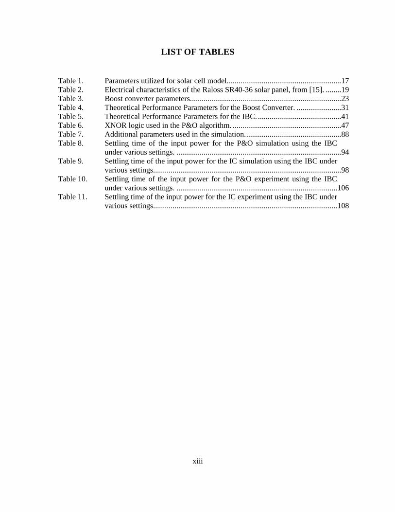
LIST OF TABLES
Table 1. Parameters utilized for solar cell model...........................................................17 Table 2. Electrical characteristics of the Raloss SR40-36 solar panel, from [15]. ........19 Table 3. Boost converter parameters..............................................................................23 Table 4. Theoretical Performance Parameters for the Boost Converter. .......................31 Table 5. Theoretical Performance Parameters for the IBC. ...........................................41
Table 6. XNOR logic used in the P&O algorithm. ........................................................47 Table 7. Additional parameters used in the simulation. .................................................88 Table 8. Settling time of the input power for the P&O simulation using the IBC
under various settings. .....................................................................................94
Table 9. Settling time of the input power for the IC simulation using the IBC under
various settings.................................................................................................98
Table 10. Settling time of the input power for the P&O experiment using the IBC
under various settings. ...................................................................................106 Table 11. Settling time of the input power for the IC experiment using the IBC under
various settings...............................................................................................108

xiv
THIS PAGE INTENTIONALLY LEFT BLANK

xv
LIST OF ACRONYMS AND ABBREVIATIONS
AC alternating current
ADC analog-to-digital converter
CCM continuous conduction mode
DC direct current
DCM discontinuous conduction mode
DOD Department of Defense
EHP electron-hole pair
ESR equivalent series resistance
FPGA field-programmable gate array
GREENS Ground Renewable Expeditionary Energy Network System
IBC interleaved boost converter
IC incremental conductance
IGBT insulated gate bipolar transistor
IIR infinite impulse response
KCL Kirchhoff’s Current Law
KVL Kirchhoff’s Voltage Law
MOSFET metal-oxide semiconductor field-effect transistor
MPP maximum power point
MPPT maximum power point tracking
RCC ripple correlation control
P&O perturb and observe
PI proportional-integral
PWM pulse width modulation
PV photovoltaic
SPACES Solar Portable Alternative Communications Energy System
USMC United States Marine Corps
VHDL VHSIC hardware description language
VHSIC very high speed integrated circuit

xvi
THIS PAGE INTENTIONALLY LEFT BLANK

xvii
ACKNOWLEDGMENTS
I would like to thank my wife, Kim, for all of her support, help, and love while I
completed this thesis. I also would like to thank my lovely daughter, Molly, who has
definitely brought joy to my life while accomplishing this demanding task.
I would like to thank my family and friends, especially my mother, Kathy, and
brother, Andrew, who have supported me over the years. I appreciate their assistance and
encouragement.
Professor Giovanna Oriti spent many hours assisting me with writing this
document. Additionally, she gave me excellent guidance on how to conduct my research.
Professor Alexander Julian devoted a great deal of time in the laboratory and
elsewhere in order to ensure my hardware and computer code worked correctly.
Finally, I want to thank God for blessing me with the talents necessary to
complete this research.

xviii
THIS PAGE INTENTIONALLY LEFT BLANK
1
I. INTRODUCTION
The Department of Defense’s (DOD) energy policy “is to enhance military
capability, improve energy security, and mitigate costs in its use and management of
energy” [1, p. 1]. In order to accomplish that, the DOD has established several priorities
such as acquiring alternative energy sources and developing new technologies that help
exploit those resources [1]. Solar photovoltaic (PV) energy is just one of those
technologies that the DOD is currently pursuing.
The United States Marine Corps (USMC) has devoted itself to achieving several
energy goals that are in line with the DOD’s objectives. Among them are a few that apply
to solar PV energy. First and foremost, the USMC wants to “forge an ethos throughout
the Marine Corps equating energy and resource efficiency with combat effectiveness” [2,
pp. 21]. It has challenged itself to ensure that at least 50% of all energy consumed will
come from alternative energy by 2020 [2]. Also, the Corps has committed itself to
achieving its operational energy demands by using renewable energy sources and to
making these systems as efficient as possible [2]. Furthermore, the USMC has chosen to
fulfill these goals by using photovoltaic devices among other things. For instance, the
USMC has fielded two different solar PV systems—the Solar Portable Alternative
Communications Energy System (SPACES) and the Ground Renewable Expeditionary
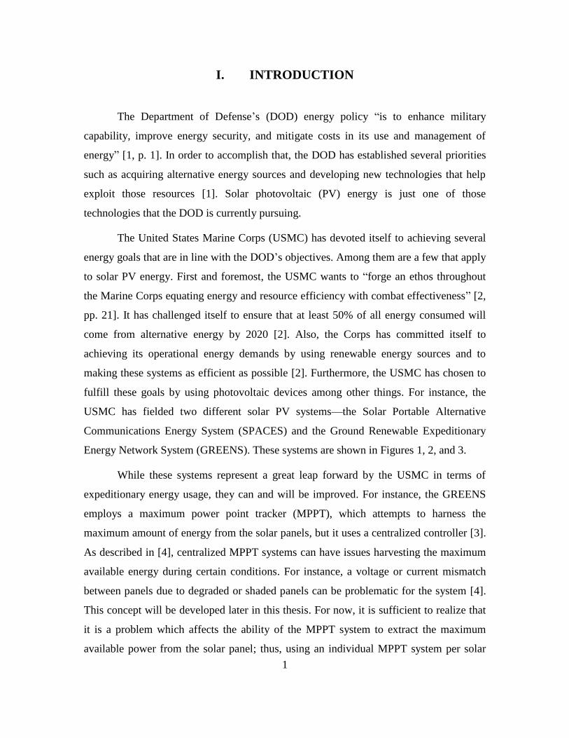
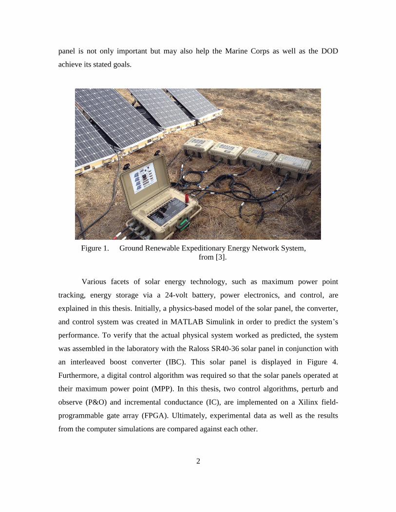
Energy Network System (GREENS). These systems are shown in Figures 1, 2, and 3.
While these systems represent a great leap forward by the USMC in terms of
expeditionary energy usage, they can and will be improved. For instance, the GREENS
employs a maximum power point tracker (MPPT), which attempts to harness the
maximum amount of energy from the solar panels, but it uses a centralized controller [3].
As described in [4], centralized MPPT systems can have issues harvesting the maximum
available energy during certain conditions. For instance, a voltage or current mismatch
between panels due to degraded or shaded panels can be problematic for the system [4].
This concept will be developed later in this thesis. For now, it is sufficient to realize that
it is a problem which affects the ability of the MPPT system to extract the maximum
available power from the solar panel; thus, using an individual MPPT system per solar
2
panel is not only important but may also help the Marine Corps as well as the DOD
achieve its stated goals.
Ground Renewable Expeditionary Energy Network System, Figure 1.
from [3].
Various facets of solar energy technology, such as maximum power point
tracking, energy storage via a 24-volt battery, power electronics, and control, are
explained in this thesis. Initially, a physics-based model of the solar panel, the converter,
and control system was created in MATLAB Simulink in order to predict the system’s
performance. To verify that the actual physical system worked as predicted, the system
was assembled in the laboratory with the Raloss SR40-36 solar panel in conjunction with
an interleaved boost converter (IBC). This solar panel is displayed in Figure 4.
Furthermore, a digital control algorithm was required so that the solar panels operated at
their maximum power point (MPP). In this thesis, two control algorithms, perturb and
observe (P&O) and incremental conductance (IC), are implemented on a Xilinx field-
programmable gate array (FPGA). Ultimately, experimental data as well as the results
from the computer simulations are compared against each other.

3
A Marine sets up the SPACES, from [5]. Figure 2.
A. PURPOSE
In this part of the introduction, the purpose of this thesis research, which is related
to the expeditionary energy goals, is discussed. Given the goals as stated in the previous
section as well as other interests, the purpose of this research can be summarized as
follows:
To emphasize the importance of using a MPPT with a solar array.
To highlight the advantages of using a MPPT on each solar panel.
To describe how one can use a tracking algorithm to maximize the
production of the available energy from a solar panel.
To demonstrate how digitally controlled power electronics interfaced to a
solar panel can achieve the highest efficiency possible in order to power a
load.
Ideally, if the goals of this research can be implemented, then the DOD energy
goals may be advanced, bringing the DOD one step closer to its energy goals being
realized.
4
Marines employ the GREENS, from [3]. Figure 3.
Raloss SR40-36 solar panel. Figure 4.

5
B. RESEARCH OBJECTIVES
The objectives of this research are defined as those things that must be done in
order to accomplish the stated purpose. Based on the purpose of this thesis, the objectives
for this research have been determined and are summarized as follows:
Detail the physics of a solar cell at a fundamental level.
Model a solar panel using physics-based equations.
Construct an interleaved boost converter so that it can power a load and
charge a battery simultaneously.
Simulate the solar PV system so that the performance may be predicted.
Implement at least two maximum power point tracking algorithms in order
to track the MPP of a solar panel.
Test and record the results of the actual system in order to verify the
physics-based model.
Compare the results against the simulations and evaluate the MPPT
algorithms that were utilized against each other.
C. RELATED WORK
In this part of the introduction, other related research that has been previously
conducted is briefly discussed in a general sense. Also, the differences of this research in
relation to earlier work are presented. Previous literature presented and compared
different maximum power point tracking (MPPT) algorithms for various PV systems.
There are literally thousands of documents that chronicle MPPT algorithms, and they are
too numerous to name here. Later in this thesis, various MPPT algorithms are explained.
Moreover, the two algorithms that are used in this thesis research are fairly traditional
and have been explored by other researchers. However, in this thesis, these two
algorithms are investigated in more detail than most. Additionally, many different types
of power converters have been used to control these types of systems. For instance,
various DC-to-DC converters, such as the buck, boost, buck-boost, forward, SEPIC,
resonant, flyback, and others, as well as DC-to-AC inverters have been used in the
implementation of a MPPT system. Interleaving techniques like the one described here

6
also have been employed but to a lesser extent. In this thesis, certain aspects of the
interleaved boost converter are explored and explained more fully. A unique aspect of
this research is that the MPPT algorithms are synthesized via the Xilinx blockset within
Simulink and other Xilinx software. Then the algorithms are loaded into a FPGA for
usage. Succinctly put, the novel contribution of this thesis is to present both simulations
and experiments of two digitally implemented MPPT techniques utilizing an interleaved
boost converter. Additionally, the level of detail with which the author presents these
topics contributes further knowledge of these subjects.
7
II. THEORY
A. PHOTOVOLTAIC SOLAR CELL
A brief understanding of how solar cells physically work is provided in this
section, which is intended to provide the reader with a fundamental explanation of the
physics involved as well as the mathematical equations used to model a solar cell.
1. Basic Physics
In order to understand how a solar cell physically works, one must have a
fundamental grasp of how a diode operates. Diodes are made of semiconductor materials
such as germanium and silicon. For the purposes of this discussion, it is assumed that the
main element within the semiconductor under consideration is silicon since it is the most
prevalent; however, other semiconductor materials are used to make diodes, solar cells,
transistors, and other electronic components.
a. Basic Physics of a Diode
Referencing the periodic table of elements, silicon is a group 4 element, which
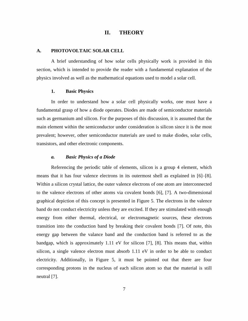
means that it has four valence electrons in its outermost shell as explained in [6]–[8].
Within a silicon crystal lattice, the outer valence electrons of one atom are interconnected
to the valence electrons of other atoms via covalent bonds [6], [7]. A two-dimensional
graphical depiction of this concept is presented in Figure 5. The electrons in the valence
band do not conduct electricity unless they are excited. If they are stimulated with enough
energy from either thermal, electrical, or electromagnetic sources, these electrons
transition into the conduction band by breaking their covalent bonds [7]. Of note, this
energy gap between the valance band and the conduction band is referred to as the
bandgap, which is approximately 1.11 eV for silicon [7], [8]. This means that, within
silicon, a single valence electron must absorb 1.11 eV in order to be able to conduct
electricity. Additionally, in Figure 5, it must be pointed out that there are four
corresponding protons in the nucleus of each silicon atom so that the material is still
neutral [7].
8
Silicon crystal lattice showing covalent bonds, from [6]. Figure 5.
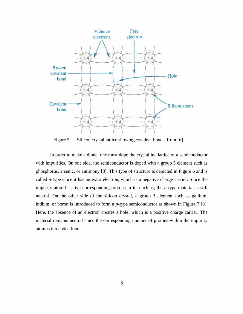
In order to make a diode, one must dope the crystalline lattice of a semiconductor
with impurities. On one side, the semiconductor is doped with a group 5 element such as
phosphorus, arsenic, or antimony [8]. This type of structure is depicted in Figure 6 and is
called n-type since it has an extra electron, which is a negative charge carrier. Since the
impurity atom has five corresponding protons in its nucleus, the n-type material is still
neutral. On the other side of the silicon crystal, a group 3 element such as gallium,
indium, or boron is introduced to form a p-type semiconductor as shown in Figure 7 [8].
Here, the absence of an electron creates a hole, which is a positive charge carrier. The
material remains neutral since the corresponding number of protons within the impurity
atom is three vice four.
9
Pentavalent impurity injected into the crystalline lattice creating an Figure 6.
n-type semiconductor, from [6].
Trivalent impurity injected into the crystalline lattice creating a p-Figure 7.
type semiconductor, from [6].

10
At the p-n junction where these two types of materials meet within the silicon
crystal, some interesting things happen. First, a process known as diffusion takes place.
Diffusion is the process by which charge carriers move from a place of high
concentration to a place of lower concentration; hence, some of the holes within the p-
type material diffuse to the n-type side [6]. This is because holes, which are the majority
charge carriers on the p-type side, are in high concentration on that side, but they are in
low concentration on the n-type side [6]–[8]. Likewise, some of the electrons within the
n-type material diffuse to the p-type side. This produces a fascinating phenomenon at the
junction. Since electrons have moved from the n-type material to the p-type material,
they recombine with the majority holes [6]. This causes a portion of the p-type material to
become negatively charged due to the fact that the impurity atoms there have only three
corresponding protons compared to the four valence electrons. Also, these trivalent
impurity atoms are sometimes called acceptors since their holes can more easily accept
electrons [6]–[8]. This is because it takes less energy to form a covalent bond [7].
Similarly, the holes that diffused from the p-type material into the n-type material
recombine with the majority electrons on the n-type side [6]. Thus, this portion of the n-
type material becomes positively charged since the impurity atoms on the n-type side
now have five protons that correspond to only four outer shell electrons. Additionally,
these pentavalent impurity atoms are sometimes called donors since they can more easily
donate their free electron [6]–[8]. In other words, it takes less energy to separate these
free electrons from its attraction to its atom [7].
Consequently, an electric field is created at the p-n junction since the n-type
material is positively charged with respect to the p-type material [6]–[8]. When in
equilibrium, this electric field restricts additional diffusion of holes and electrons due to
its polarity [6]–[8]. To understand why this works, consider the following example under
open-circuit conditions. As previously stated, the electrons in the n-type material want
move to towards the p-type region due to diffusion current. At some point, the electric
field becomes strong enough that these electrons cannot diffuse anymore and are repelled
back towards the n-type side. A similar explanation can be made for holes on the p-type
side. Furthermore, the material in the vicinity of the junction is called the depletion
11
region (or space-charge region) because it has been depleted of all of its charge carriers
[6]. In Figure 8, a depiction of the depletion region is portrayed with its electric field.
Forward-biased diode, after [9]. Figure 8.
The depletion region gives rise to an additional mechanism called drift. Drift is
the process by which charge carriers are influenced by an electric field. Holes, which are
deemed positive, drift in the direction of the electric field from the positively charged
side to the negatively charged side [6]. On the other hand, electrons, which are designated
as negative, drift in the opposite direction of the electric field from the negative side to
the positive side [6]. One must remember that the positively charged side is n-type, and
the negatively charged side is p-type; thus, drift current due to the p-n junction’s electric
field works in the opposite direction of the diffusion current. As explained in [6], holes
on the n-type side and electrons on the p-type side move across the junction due to drift
current. When in proximity of the depletion region and under the influence of its electric
field, these minority carriers, which are dependent on temperature, are swept across the
junction due to the polarity of the electric field [6]–[7]. Lastly, based on [6], it can be
shown mathematically that the forward-biased current through a diode can be written as
12
1D S S S S
t t
I I I I exp I I expn
v
V nV
v
(1)
where ID is the diffusion current, IS is the drift current, n is the ideality factor, v is external
voltage across the diode, and Vt is the thermal voltage at the junction’s temperature. One
must realize that the reference direction for the current I is from the diode’s positive
terminal to its negative terminal. This is important later when analyzing the current
through a solar cell.
b. Basic Physics of a Solar Cell
Since many of the basic concepts about diodes have been clarified, the following
discussion focuses on the physics behind the operation of a solar cell. The first thing to
understand is the notion of electromagnetic energy contained in photons. Photons are the
fundamental particles that propagate electromagnetic waves. They are considered to be
without mass and do not have any electric charge [10]–[11]. Also, according to Max
Planck and Albert Einstein, photons can only exist in quantized levels of energy [10].
That is, they can only attain specific, discrete energy levels as opposed to any arbitrary
amount of energy in between those levels [10]. Moreover, Planck discovered that matter
absorbs and emits light in distinct quantities of energy, or “packets” of energy [10]. The
energy E contained in one photon was shown to be
hc
E
(2)
in accordance with [7], [8], and [10], where h is Planck’s constant (6.626×10⁻³⁴
J·s), c is
the speed of light (3.0×10⁸ m/s), and λ is the wavelength of the photon. If one inserts the
bandgap energy of silicon, which is 1.11 eV, into (2), one can solve for the corresponding
wavelength. As stated in [8], only photons that have a wavelength of 1.12 μm or less are
able to generate the energy necessary to separate an electron from its covalent bond so
that it may enter the conduction band. This is the fundamental process that makes the
photoelectric effect, which Planck and Einstein first theorized, possible.
When a solar PV cell is exposed to electromagnetic radiation via sunlight, a
tremendous number of photons are injected into the material. Some of these photons are

13
absorbed by electrons and energize them [8], [11]. Provided these photons possess the
required amount of energy, they cause electrons within the material to break free from
their covalent bonds [8], [11]. As a result, these photons create a number of electron-hole
pairs (EHP), which are swept across the electric field of the solar cell via the drift
principle discussed earlier. Electrons, whether they are generated in the p-type or n-type
region, are forced to flow towards the terminal on the n-type side. Once they arrive at that
terminal, they flow through the external circuit to power a load. Eventually, the electrons
reach the terminal on the p-type side, where they are injected back into the solar cell [11].
Additionally, the creation of an EHP causes a hole to be left behind. This allows other
valence electrons that are in adjacent atoms to move and take the place of this hole [11].
This leaves behind another hole, and this process repeats itself until, by chance, an
electron recombines with this hole [11]. Accordingly, these valence electrons move in the
same direction as the conduction electrons, but the holes appear to move in the opposite
direction. Ultimately, holes, whether they are created in the p-type or n-type material, are
driven to the terminal on the p-type side, where they recombine with electrons from the
external circuit [11].
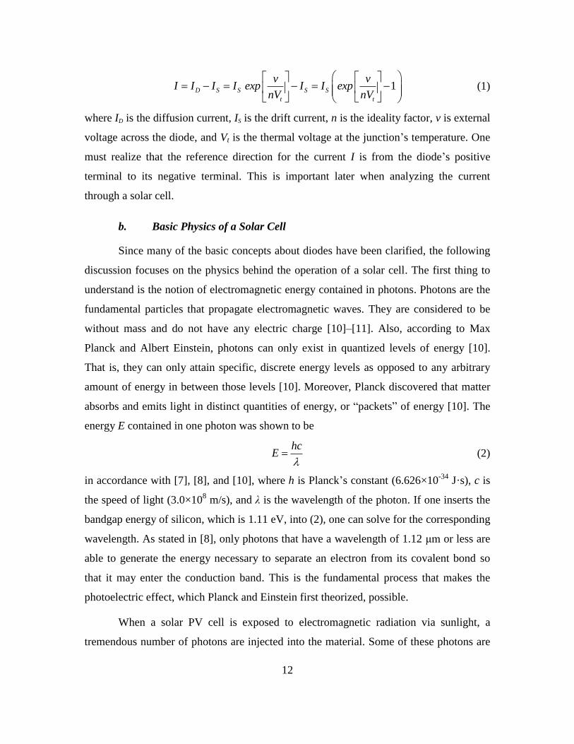
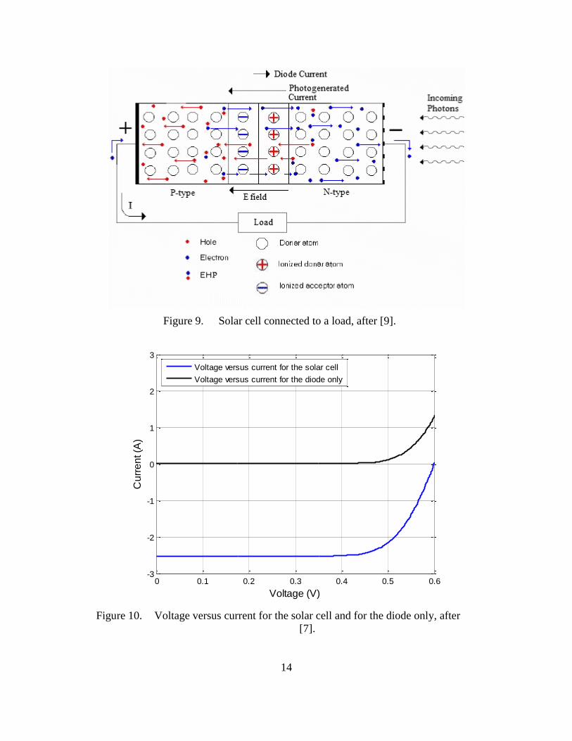
In Figure 9, the flow of electric current and overall operation of a solar cell is
illustrated. It is important to note that the reference direction for the current I is in the
opposite direction to that of a diode. If one were to use the same reference direction that
the diode uses for the current, then the voltage versus current plot, which is also known as
the I-V curve, would be similar to Figure 10. Here, the solar cell’s I-V curve is contrasted
against its diode only current. The diode current is the only current that results if the solar
cell is not generating any photocurrent. In other words, if the solar cell is placed in the
dark and then subjected to the corresponding voltages, it operates just like a diode [8].
For a solar cell, one typically flips the I-V curve on its head to produce the more familiar
plots that are presented in Figures 12 and 14. Realize that doing this is akin to reversing
the reference direction of the current I as is shown in Figure 9.
14
Solar cell connected to a load, after [9]. Figure 9.
Voltage versus current for the solar cell and for the diode only, after Figure 10.
[7].
0 0.1 0.2 0.3 0.4 0.5 0.6-3
-2
-1
0
1
2
3
Voltage (V)
Cu
rre
nt (A
)
Voltage versus current for the solar cell
Voltage versus current for the diode only
15
Based on the physical interactions within the solar cell as well as external to it,
there are several possibilities that can transpire. The following is a summary of those
scenarios, and this list, while not all inclusive, helps to explain the low efficiency of solar
photovoltaic energy conversion.
Photons are either reflected or absorbed in the atmosphere [11]. This is
energy from the sun that does not even make it to the solar cell. While this
does not account for the low efficiency, some of this energy could be
collected provided the environmental conditions were more suitable.
Photons reflect off the surface of the solar cell. These particles may strike
the surface at a poor angle or may collide with the electric contacts on top
of the cell [7], [11]. Either way, they are reflected and are not absorbed by
the solar cell. Textured surfaces and anti-reflective coatings help to
prevent photons from reflecting off the surface of the solar cell [7], [8].
A photon of sufficient energy is absorbed by an electron and creates an
EHP, but the electron and/or hole ends up recombining internally prior to
producing a current external to the solar cell [7].
Photons of sufficient energy are absorbed by numerous electrons and
create many EHPs. Subsequently, the electrons are collected so that an
electric current is created in the external circuit [7], [11]. Once the
electrons are outside the solar cell, there is no threat of recombination.
While this is the best and desired outcome, this current still has to flow
through ohmic contacts and electrical wires as well as resistance within in
the semiconductor itself; hence, this scenario is not without its own losses
[7].
A photon does not strike an electron and passes through the material
without creating an EHP [11]. This problem can be mitigated by using
back-surface reflectors as mentioned in [7].
A low energy photon is absorbed by an electron but does not create an
EHP since it cannot raise the electron’s energy enough to move it into the
conduction band [7], [11]. This excess energy is converted into heat [7],
[11].
A high energy photon, also referred to as a phonon, is absorbed by an
electron and creates an EHP [7], [11]. In this case, the amount of energy
that exceeds the bandgap energy causes lattice vibrations and is
transformed into heat [7], [11].
16
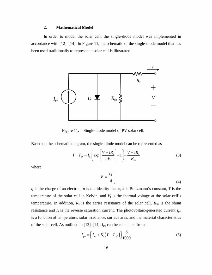
2. Mathematical Model
In order to model the solar cell, the single-diode model was implemented in
accordance with [12]–[14]. In Figure 11, the schematic of the single-diode model that has
been used traditionally to represent a solar cell is illustrated.
Single-diode model of PV solar cell. Figure 11.
Based on the schematic diagram, the single-diode model can be represented as
1s sph S
t sh
V IR V IRI I I exp
nV R
(3)
where
t
kTV
q
, (4)
q is the charge of an electron, n is the ideality factor, k is Boltzmann’s constant, T is the
temperature of the solar cell in Kelvin, and Vt is the thermal voltage at the solar cell’s
temperature. In addition, Rs is the series resistance of the solar cell, Rsh is the shunt
resistance and IS is the reverse saturation current. The photovoltaic-generated current Iph
is a function of temperature, solar irradiance, surface area, and the material characteristics
of the solar cell. As outlined in [12]–[14], Iph can be calculated from
1000
ph sc i ref
SI I K T T
(5)
Rs
Iph Rsh D V
I
17
where S is the solar irradiance in W/m2, T is the temperature of the solar cell, Tref is the
reference temperature of 25 ºC (298.15 K), and Isc is the short-circuit current of the solar
cell at a solar irradiance of 1000 W/m2 assuming a reference temperature of 25 ºC. Lastly,
Ki is the short-circuit current temperature coefficient and was chosen to be 0.0017 A per
ºC based on [12] and [13]. Like the photo-generated current, the reverse saturation
current Is can be adjusted for temperature as well using
3
, 1 g
s s ref
ref ref t
ET TI I exp
T T nV
(6)
in accordance with [12]–[14]. Here, it must be noted that the temperature T and the
reference temperature Tref must be calibrated in Kelvin. Also, Is,ref is the reverse saturation
current at the reference temperature, and Eg is the bandgap energy of the solar cell
material, which is silicon in this case. The reverse saturation current Is is a function of
temperature as well as the material characteristics of the solar panel. In Table 1, the
parameters that were used in this thesis to simulate the solar cell are summarized.
Table 1. Parameters utilized for solar cell model.
Parameter Symbol Value
Series Resistance Rs 0.01717 Ω
Shunt Resistance Rsh 1000 Ω
Reverse Saturation Current @ 25 ºC Is,ref 3.12x10
-8 A
Bandgap Energy of Silicon Eg 1.11 eV
Ideality Factor n 1.282
Short Circuit Current Temperature Coefficient Ki 0.0017 A per ºC
Boltzmann’s Constant k 1.3806488x10⁻²³
J/K
Charge of an electron q 1.602176565x10⁻¹⁹
C
With (3) and (4), one can create a mathematical model in order to simulate a solar
panel, also known as a module, or even an entire array. Of note, a solar panel or module
can be defined as a collection of solar cells that are usually connected in series, and a
solar array is multiple solar modules that are connected in series, parallel, or some
combination. Up to this point, the model presented applies to just one solar cell. In order
to have it pertain to a solar panel or an entire array of solar panels, some modifications
18
must be made. For one, it is assumed that every solar cell in the entire array experiences
the same solar irradiance, temperature, and incidence angle. Additionally, one must
transform the voltage VIN and current IIN at the terminals of the solar panel (or array) into
the voltage V and current I experienced by just one cell. Since voltage is distributed
equally when elements are joined in series, V = VIN ÷ Ns. Also, current is spread evenly
amongst components connected in parallel, so I = IIN ÷ Np. In these equations, the number
of cells in series is Ns, and the number of strings of series-connected cells in parallel is Np.
With these adjustments, one can use the single cell model to simulate a solar panel (or
array); hence, (3) becomes
1
IN IN IN INs s
s p s p
ph s
t sh
V I V IR R
N N N NI I I exp
nV R
. (7)
Once the new, updated current I for the solar cell is calculated from (7), the
array’s updated current IIN can be found by multiplying I by Np. Notice that if one is
simulating just a single module (assuming all of its cells are connected in series), then Np
is equal to one. Thus, IIN and I are equal. Since the solar cell is modeled as a current
source, the external circuit, which is connected to the solar panel (or array), governs what
the new, updated voltage VIN is across its terminals. As a side note, if two or more solar
panels are connected in series, which is done in some solar arrays, the voltage across each
panel can be found by dividing VIN by the number of panels in series. See Chapter IV and
Appendix B for more details of how this model was created in Simulink.
Subsequently, one can utilize the mathematical model previously presented to create
the model of the solar panel used in this thesis. To achieve this, some of the variables in
Table 1 were altered multiple times until the desired electrical characteristics of the solar
panel, which are displayed in Table 2, were finally obtained. Namely, Rs, n, and Is,ref were
manipulated to obtain the correct characteristics as seen in Table 2. Of note, these
characteristics represent that of the Raloss SR40-36 solar panel when tested in standard test
conditions, which are 1000 W/m2, 25ºC, and an air mass of 1.5 as defined in [11].
19
Table 2. Electrical characteristics of the Raloss SR40-36 solar panel, from [15].
Parameter Symbol Value
Open Circuit Voltage Voc 21.6 V
Short Circuit Current Isc 2.54 A
Maximum Power Point Voltage Vmpp 17.0 V
Maximum Power Point Current Impp 2.36 A
As mentioned before, the characteristics of the solar panel listed in Table 2 are
achieved by adjusting the settings of the mathematical model. After that, one can create
various plots of its performance under certain circumstances. For instance, one can make
current versus voltage and power versus voltage plots for different levels of irradiance
assuming the temperature remains constant as in Figures 12 and 13. Additionally, in
Figures 14 and 15, current versus voltage and power versus voltage plots were generated
for different temperature levels assuming the solar irradiance remained constant.
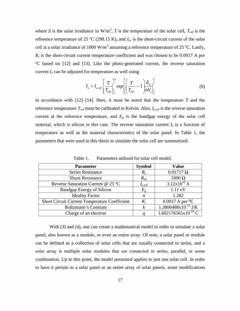
Current versus voltage for varying levels of irradiance at 25 ºC. Figure 12.
20
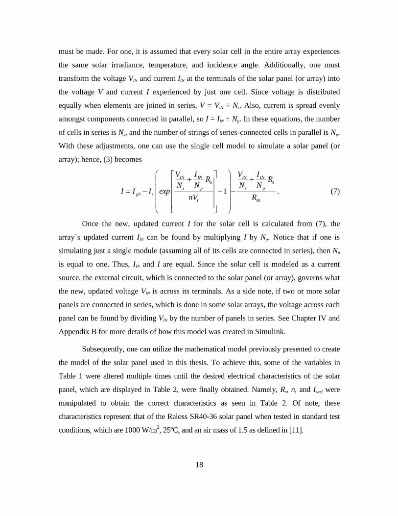
Power versus voltage for varying levels of irradiance at 25 ºC. Figure 13.
Current versus voltage for varying levels of temperature at 1000 Figure 14.
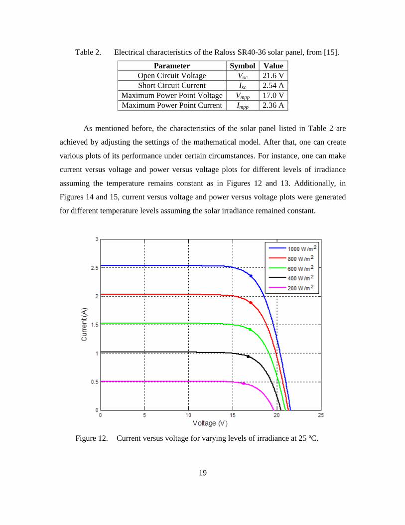
W/m2.
0 5 10 15 20 250
5
10
15
20
25
30
35
40
45
Po
we
r (W
)
Voltage (V)
1000 W/m2
800 W/m2
600 W/m2
400 W/m2
200 W/m2
21
Power versus voltage for varying levels of temperature at 1000 Figure 15.
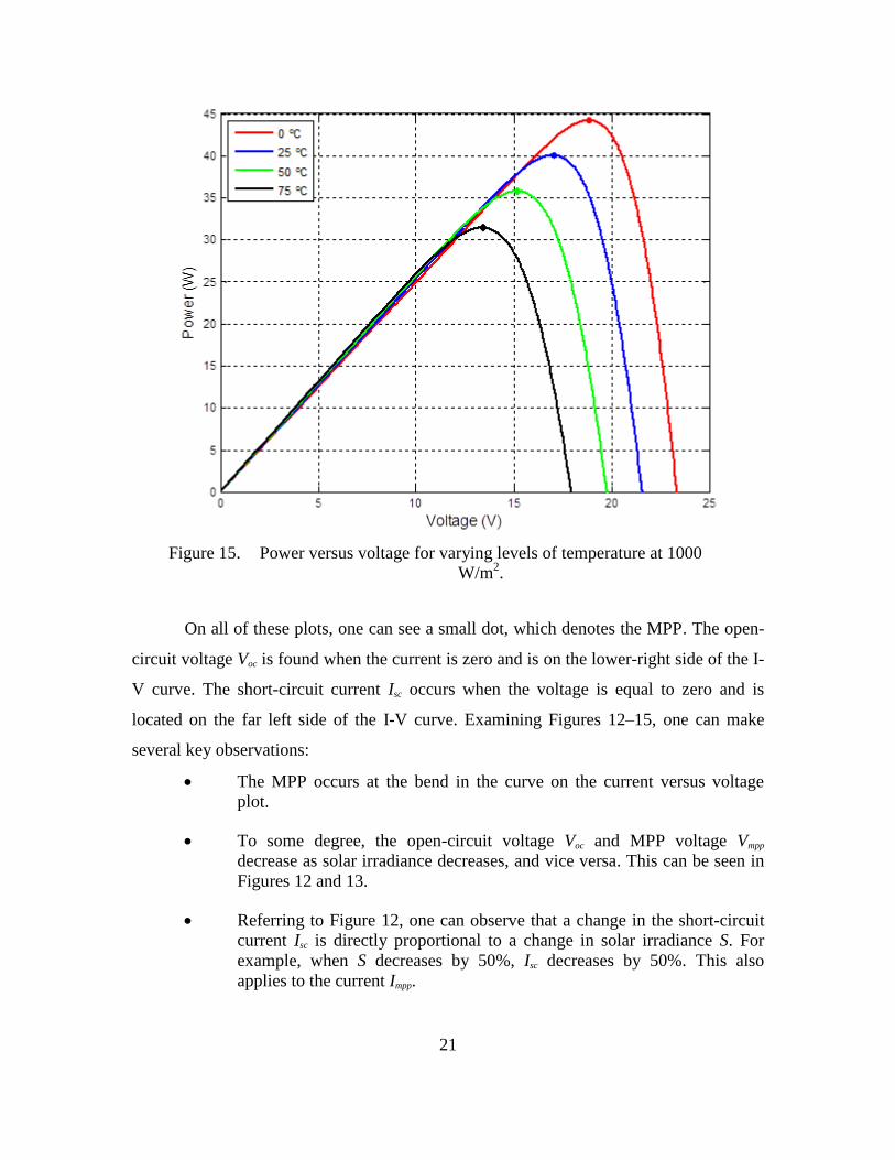
W/m2.
On all of these plots, one can see a small dot, which denotes the MPP. The open-
circuit voltage Voc is found when the current is zero and is on the lower-right side of the I-
V curve. The short-circuit current Isc occurs when the voltage is equal to zero and is
located on the far left side of the I-V curve. Examining Figures 12–15, one can make
several key observations:
The MPP occurs at the bend in the curve on the current versus voltage
plot.
To some degree, the open-circuit voltage Voc and MPP voltage Vmpp
decrease as solar irradiance decreases, and vice versa. This can be seen in
Figures 12 and 13.
Referring to Figure 12, one can observe that a change in the short-circuit
current Isc is directly proportional to a change in solar irradiance S. For
example, when S decreases by 50%, Isc decreases by 50%. This also
applies to the current Impp.

22
When the solar irradiance changes, the associated power at the MPP Pmpp
varies by nearly the same percentage as seen in Figure 13. For instance,
when S decreases from 1000 to 200 W/m2, an 80% decrease, Pmpp
decreases by almost 80% as well. In fact, it actually decreases by
something slightly more than 80%.
The slopes of the power versus voltage curve become steeper with higher
levels of irradiance. This fact makes it easier to find the MPP at higher
irradiance values.
When the temperature of the solar cell increases, Voc and Vmpp decrease
noticeably as witnessed in Figures 14 and 15. These voltages change by
about 0.072–0.075 V per ºC for this particular solar cell.
Referencing Figure 14, one sees that the short-circuit current Isc increases
only slightly as the temperature is raised. As previously stated, Isc
increases by 0.0017 A per ºC when the temperature goes up.
As temperature is varied, Impp stays about the same as is observed in Figure
14.
As the temperature increases, Pmpp goes down significantly as in Figure 15.
For this solar cell, Pmpp goes down by approximately 0.17 W per ºC.
The slopes of the power versus voltage curve in Figure 15 stay relatively
constant as temperature is changed.
B. DC-DC POWER CONVERTER
In this portion of the thesis, the power electronics used in this research are
discussed. The boost converter topology and associated mathematical equations are
explained in accordance with [16]–[19]. Furthermore, several of the qualities of the
interleaved boost converter as described in [20] and [21] are elaborated upon.
1. Boost Converter
In this thesis, a DC-to-DC power converter was operated as an essential
connection between the solar panel and the load. Moreover, the boost converter was
selected as the baseline power converter. This power converter is the mechanism by
which MPPT is achieved. One can examine the overall layout of the boost converter
topology and how it interfaces with the rest of the solar PV system in Figure 16. Here,
one observes that the solar panel connects to the input side of the converter while the load
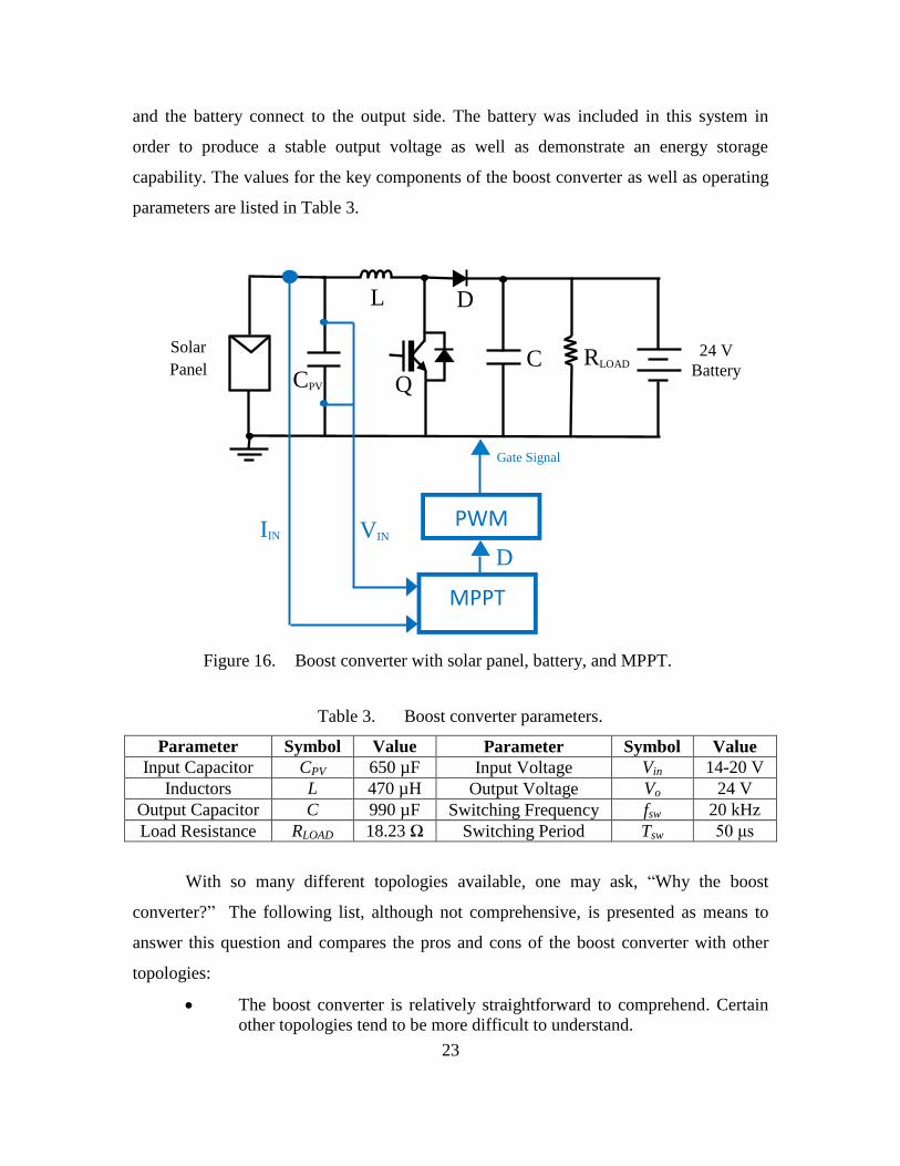
23
and the battery connect to the output side. The battery was included in this system in
order to produce a stable output voltage as well as demonstrate an energy storage
capability. The values for the key components of the boost converter as well as operating
parameters are listed in Table 3.
Boost converter with solar panel, battery, and MPPT. Figure 16.
Table 3. Boost converter parameters.
Parameter Symbol Value Parameter Symbol Value
Input Capacitor CPV 650 µF Input Voltage Vin
14-20 V
Inductors L 470 µH Output Voltage Vo 24 V
Output Capacitor C 990 µF Switching Frequency fsw 20 kHz
Load Resistance RLOAD 18.23 Ω Switching Period Tsw 50 μs
With so many different topologies available, one may ask, “Why the boost
converter?” The following list, although not comprehensive, is presented as means to
answer this question and compares the pros and cons of the boost converter with other
topologies:
The boost converter is relatively straightforward to comprehend. Certain
other topologies tend to be more difficult to understand.
24 V
Battery
Solar
Panel RLOAD
L D
C Q
CPV
MPPT
IIN
D
PWM VIN
Gate Signal

24
The switch is connected to ground, which makes the insulated gate bipolar
transistor (IGBT) easier to drive.
The diode prevents current from the battery from flowing back into the
solar panel and potentially causing damage [22].
The boost converter increases the panel’s voltage to that required to
charge the 24 V battery; thus, it makes the panel’s voltage compatible with
the battery’s voltage.
A drawback of the boost converter is that it requires a ballast load [18]. If
there is not at least a ballast load at the output, then the output voltage
climbs excessively and damages the output capacitor.
The boost converter can only increase the output voltage to a value that is
higher than the input voltage. This fact makes the boost converter
unsuitable for a system with an output voltage that is lower than the solar
panel’s VMPP. In fact, one would want the output voltage to be, at least,
slightly higher than the solar panel’s VMPP for control purposes.
a. Derivation of Parameters
In order to gain some insight into the performance of the boost converter, the
following derivation of some of its basic parameters is necessary. To simplify the
derivation, the input voltage vIN is assumed to be relatively constant over short periods of
time since CPV is large enough to handle the input ripple current. Likewise, the output
voltage vOUT is assumed to be relatively constant since C is large [16]. Furthermore, the
resistive load and battery can be thought of as an equivalent load R, which is the output
voltage vOUT divided by the output current iOUT. Also, for the meantime, the energy losses
in the components are ignored, and the converter is assumed to operate in continuous
conduction mode (CCM). CCM means that the inductor L is always conducting some
current. With these assumptions in mind, one can redraw the circuit as in Figure 17.
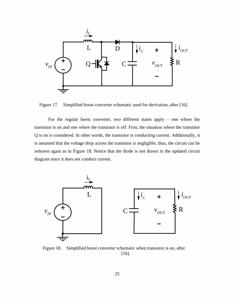
25
Simplified boost converter schematic used for derivation, after [16]. Figure 17.
For the regular boost converter, two different states apply – one where the
transistor is on and one where the transistor is off. First, the situation where the transistor
Q is on is considered. In other words, the transistor is conducting current. Additionally, it
is assumed that the voltage drop across the transistor is negligible; thus, the circuit can be
redrawn again as in Figure 18. Notice that the diode is not drawn in the updated circuit
diagram since it does not conduct current.
Simplified boost converter schematic when transistor is on, after Figure 18.
[16].
iC
vIN
iOUT
iL
L D
R C Q v
OUT
iC
vIN
iOUT
iL
L
R C vOUT

26
At this point, one can write down some basic differential equations to describe the
operation of this converter. As outlined in [16]–[18],
LIN L
div v L
dt (8)
can be found by using the left-hand side of the circuit subject to Kirchhoff’s Voltage Law
(KVL) and the simple definition of voltage across an inductor. Furthermore, diL/dt can be
approximated as the change in current divided by the change in time. If the change in
time occurs only during the time the transistor is on, one can write
IN L L
sw
v i i
L t DT
(9)
where D is the duty cycle of the transistor, and Tsw is the switching period. Logically, one
can then obtain
MAX MININ sw
L
v DTi i i
L , (10)
which is a key equation that is used later to characterize the inductor current.
Next, if one looks at the right-hand side of the circuit,
OUTC
dvi C
dt (11)
can be established by using the basic definition of current through a capacitor. Using
Kirchhoff’s Current Law (KCL), one finds that iC equals –iOUT. Thus, one obtains
OUTOUT
sw
vi C
DT
, (12)
which further simplifies to
( ) ( )OUT sw OUT sw
OUT OUT MIN OUT MAX
i DT v DTv v v
C RC (13)
in accordance with [16]–[18]. When the transistor is on, the output voltage decreases so
the ΔvOUT term is defined as vOUT(MIN) minus vOUT(MAX). Notice that R is the equivalent output
resistance seen by the converter, as previously mentioned.
After examining the scenario where the transistor is turned on, the situation where
the transistor is off is analyzed assuming CCM. In Figure 19, the equivalent circuit has
been drawn with the diode missing since it is assumed that its voltage drop is negligible.
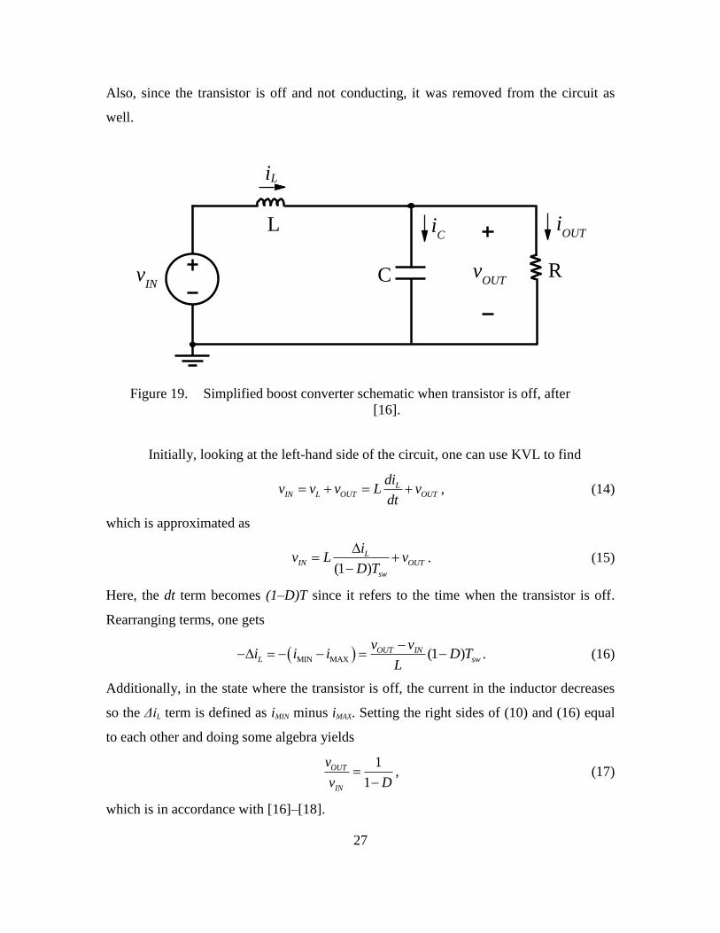
27
Also, since the transistor is off and not conducting, it was removed from the circuit as
well.
Simplified boost converter schematic when transistor is off, after Figure 19.
[16].
Initially, looking at the left-hand side of the circuit, one can use KVL to find
LIN L OUT OUT
div v v L v
dt , (14)
which is approximated as
(1 )
LIN OUT
sw
iv L v
D T
. (15)
Here, the dt term becomes (1–D)T since it refers to the time when the transistor is off.
Rearranging terms, one gets
MIN MAX (1 )OUT INL sw
v vi i i D T
L
. (16)
Additionally, in the state where the transistor is off, the current in the inductor decreases
so the ΔiL term is defined as iMIN minus iMAX. Setting the right sides of (10) and (16) equal
to each other and doing some algebra yields
1
1
OUT
IN
v
v D
, (17)
which is in accordance with [16]–[18].
iC
vIN
iOUT
iL
L
R C vOUT

28
Subsequently, the right-hand side of the circuit in Figure 19 is analyzed. At this
point, one can use KCL to sum the currents and produce
OUT OUTL OUT C
v dvi i i C
R dt . (18)
After a little manipulation, one gets
1OUT OUT
L
dv vi
dt C R
, (19)
which can also be written as
( ) ( )
11 OUT
OUT OUT MAX OUT MIN sw L
vv v v D T i
C R
. (20)
If one equates the result in (20) to (13) and does a little arithmetic, one obtains
(1 )
OUTL
vi
R D
, (21)
which is the average inductor current [16]. One can also write (21) as
2(1 )
INL
vi
R D
(22)
by substituting in (17). Assuming the converter is operating in CCM, one adds half of ΔiL
from (10) to (22), which gives
2(1 ) 2
IN IN swMAX
v v DTi
R D L
(23)
as shown in [15]. Likewise, subtracting half of ΔiL from (10) to (22) gives
2(1 ) 2
IN IN swMIN
v v DTi
R D L
. (24)
If one sets the iMIN term equal to zero and solves for L, one gets
2
12
swcrit
RDTL D , (25)
which is the critical inductance [16]–[18]. The critical inductance is the inductance where
the converter operates on the border of CCM and discontinuous mode (DCM) [16]–[18].
In other words, the inductor is always conducting except for one small instant in time
when its current reaches zero. After that moment, the inductor current does not remain at
zero as in DCM but begins to climb again. Also, one can use (24) to solve for

29
2
2
(1 )crit
sw
LR
DT D
, (26)
which is the critical resistance. If the output resistance R gets larger than the critical
resistance Rcrit, the converter is forced into DCM.
Using some of these relationships, one can also solve for the ripple in the input
voltage; however, the method to do so is more intuitive. First, consider the definition for
the current through the input capacitor,
pv
INC pv
dvi C
dt . (27)
One can take the integral of both sides and rearrange this formula to produce
2
1
2 1
1pv
t
IN IN IN C
pv t
v v t v t i dtC
. (28)
If one can integrate the input capacitor current over the correct time interval, then one can
determine the ripple in the input voltage. Furthermore, one can see that there is an equal
amount of area above and below the iCpv = 0 line by analyzing the input capacitor current
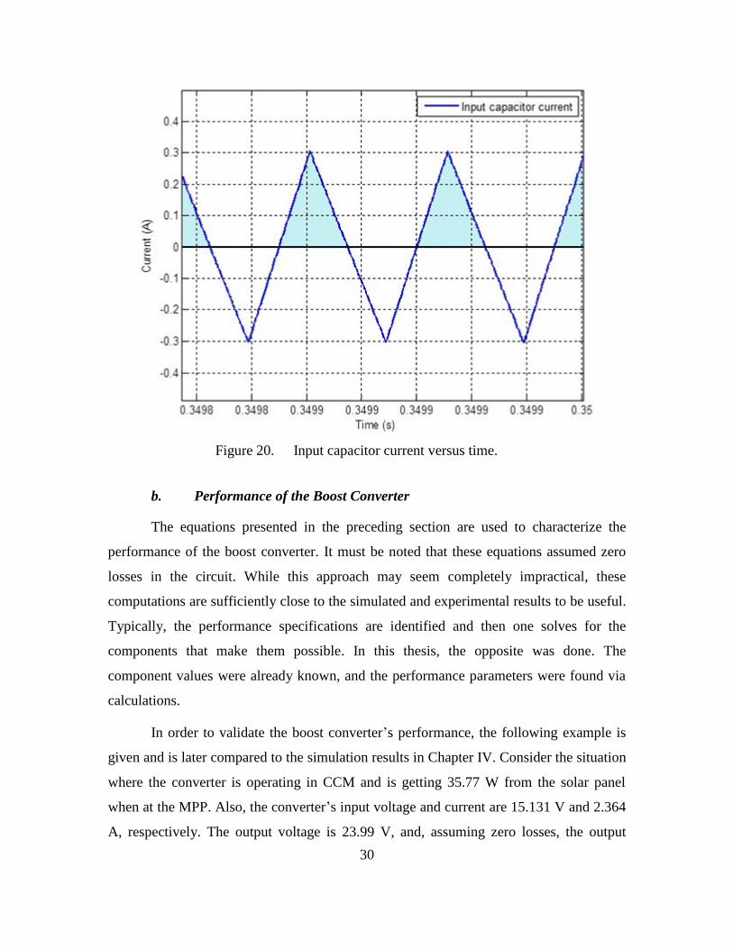
waveform shown in Figure 20. Based on this plot, notice that this waveform makes a
triangle when the current is positive (shaded in light blue). Thus, one just has to find the
area under the input capacitor current curve by using the geometry of a triangle. The base
of the triangle is given by the time that the current is positive and is half of Tsw. The
height of the triangle is determined by the change in current, which is given by dividing
the change in the inductor current ΔiL from (10) by two. Multiplying these two quantities
together and dividing by 2Cpv, one obtains the relationship,
2
1 1
2 2 2 8
IN sw IN swIN
pv pv
v DT v DTTv
L C LC
. (29)
30
Input capacitor current versus time. Figure 20.
b. Performance of the Boost Converter
The equations presented in the preceding section are used to characterize the
performance of the boost converter. It must be noted that these equations assumed zero
losses in the circuit. While this approach may seem completely impractical, these
computations are sufficiently close to the simulated and experimental results to be useful.
Typically, the performance specifications are identified and then one solves for the
components that make them possible. In this thesis, the opposite was done. The
component values were already known, and the performance parameters were found via
calculations.
In order to validate the boost converter’s performance, the following example is
given and is later compared to the simulation results in Chapter IV. Consider the situation
where the converter is operating in CCM and is getting 35.77 W from the solar panel
when at the MPP. Also, the converter’s input voltage and current are 15.131 V and 2.364
A, respectively. The output voltage is 23.99 V, and, assuming zero losses, the output
31
current must be 1.491 A. Equation (17) is used to solve for the theoretical duty cycle,
which is about 0.3693. Additionally, the theoretical equivalent resistance R is 16.09 Ω.
Using (10), one estimates the change in the inductor current ΔiL to be 594.4 mA (peak-to-
peak), or roughly 0.6 A. Likewise, the ripple in the output voltage ΔvOUT was found to be
27.8 mV using (13). Other values are found using the equations contained in the previous
section, and these theoretical calculations are summarized in Table 4.
Table 4. Theoretical Performance Parameters for the Boost Converter.
Parameter Symbol Value
Ripple in inductor current ΔiL 594.4 mA
Ripple in output voltage ΔvOUT 27.8 mV
Ripple in input voltage ΔvIN 5.72 mV
Average inductor current iL(AVG) 2.364 A
Maximum inductor current iMAX 2.661 A
Minimum inductor current iMIN 2.067 A
The critical inductance Lcrit and critical resistance Rcrit terms were found for a
worst-case scenario. Here, the duty cycle was assumed to 1/3, which is the value that
maximizes the D(1–D)2 term in (25) and (26) [17]. Also, the resistance was found by
assuming that the input current was only 1/5 of what it had been, or 472.8 mA.
Consequently, the output current is 315.2 mA since iOUT = (1–D) iIN. Since vOUT is
essentially 24 V, R equals 76.14 Ω. With that, the Lcrit was found to be 282.5 μH, and Rcrit
was calculated to be 126.9 Ω.
As mentioned earlier, the efficiency of this converter was not 100%; thus, the
values above are approximations. If one takes into account power losses, then one finds
that these values change slightly. As outlined in [19], the duty cycle is better
approximated with,
1 IN
OUT
vD
v (30)
where 𝜂 is the efficiency of the converter. It is important to note that this value for the
duty cycle D was found with a different set of assumptions; thus, it cannot be used in the
32
previously derived equations. Using (30) with an efficiency of 86%, one finds the duty
cycle to be 0.4576.
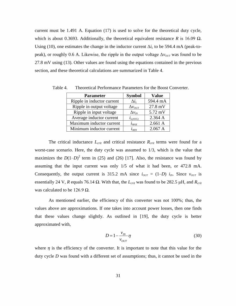
2. Interleaved Boost Converter
One of the main focuses of this thesis was to employ the interleaved boost
converter as the primary power converter topology. In [20] and [21], this layout is
chronicled extensively, where the interleaved topology consists of two parallel circuits –
each with an inductor, a diode, and a semiconductor switch. This topology is used to
control the power from the solar panel just like the regular boost converter but essentially
involves two boost converters that are placed in parallel as shown in Figure 21. Each of
these boost converters are fundamentally operated the same with the identical duty cycles
except that the timing of their operation is precisely synchronized; thus, each parallel
converter creates a current, which is interleaved to produce a total current to the load.
Furthermore, each boost converter can be thought of as a separate phase of the IBC.
Interleaved boost converter with solar panel, battery, and MPPT. Figure 21.
C Solar
Panel
L2 D2
24 V
Battery
RLOAD
L1 D1
Q2 Q1 CPV
MPPT
IIN
D
PWM VIN
Gate Signal 1
Gate Signal 2
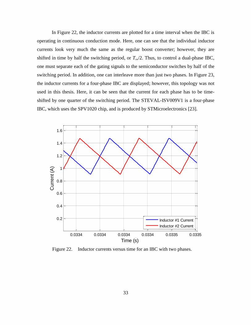
33
In Figure 22, the inductor currents are plotted for a time interval when the IBC is
operating in continuous conduction mode. Here, one can see that the individual inductor
currents look very much the same as the regular boost converter; however, they are
shifted in time by half the switching period, or Tsw/2. Thus, to control a dual-phase IBC,
one must separate each of the gating signals to the semiconductor switches by half of the
switching period. In addition, one can interleave more than just two phases. In Figure 23,
the inductor currents for a four-phase IBC are displayed; however, this topology was not
used in this thesis. Here, it can be seen that the current for each phase has to be time-
shifted by one quarter of the switching period. The STEVAL-ISV009V1 is a four-phase
IBC, which uses the SPV1020 chip, and is produced by STMicroelectronics [23].
Inductor currents versus time for an IBC with two phases. Figure 22.
0.0334 0.0334 0.0334 0.0334 0.0335 0.0335
0.2
0.4
0.6
0.8
1
1.2
1.4
1.6
Time (s)
Cu
rre
nt (A
)
Inductor #1 Current
Inductor #2 Current
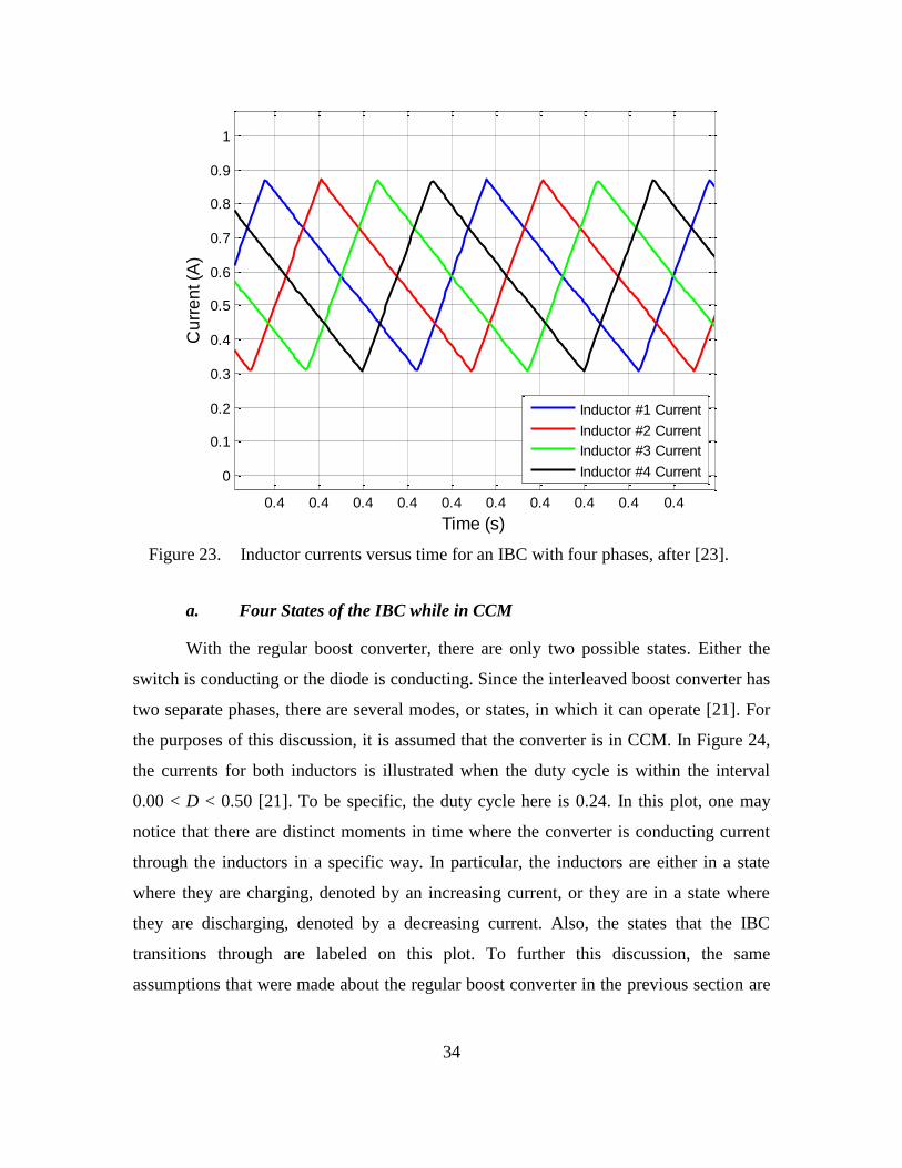
34
Inductor currents versus time for an IBC with four phases, after [23]. Figure 23.
a. Four States of the IBC while in CCM
With the regular boost converter, there are only two possible states. Either the
switch is conducting or the diode is conducting. Since the interleaved boost converter has
two separate phases, there are several modes, or states, in which it can operate [21]. For
the purposes of this discussion, it is assumed that the converter is in CCM. In Figure 24,
the currents for both inductors is illustrated when the duty cycle is within the interval
0.00 < D < 0.50 [21]. To be specific, the duty cycle here is 0.24. In this plot, one may
notice that there are distinct moments in time where the converter is conducting current
through the inductors in a specific way. In particular, the inductors are either in a state
where they are charging, denoted by an increasing current, or they are in a state where
they are discharging, denoted by a decreasing current. Also, the states that the IBC
transitions through are labeled on this plot. To further this discussion, the same
assumptions that were made about the regular boost converter in the previous section are
0.4 0.4 0.4 0.4 0.4 0.4 0.4 0.4 0.4 0.4
0
0.1
0.2
0.3
0.4
0.5
0.6
0.7
0.8
0.9
1
Time (s)
Cu
rre
nt (A
)
Inductor #1 Current
Inductor #2 Current
Inductor #3 Current
Inductor #4 Current
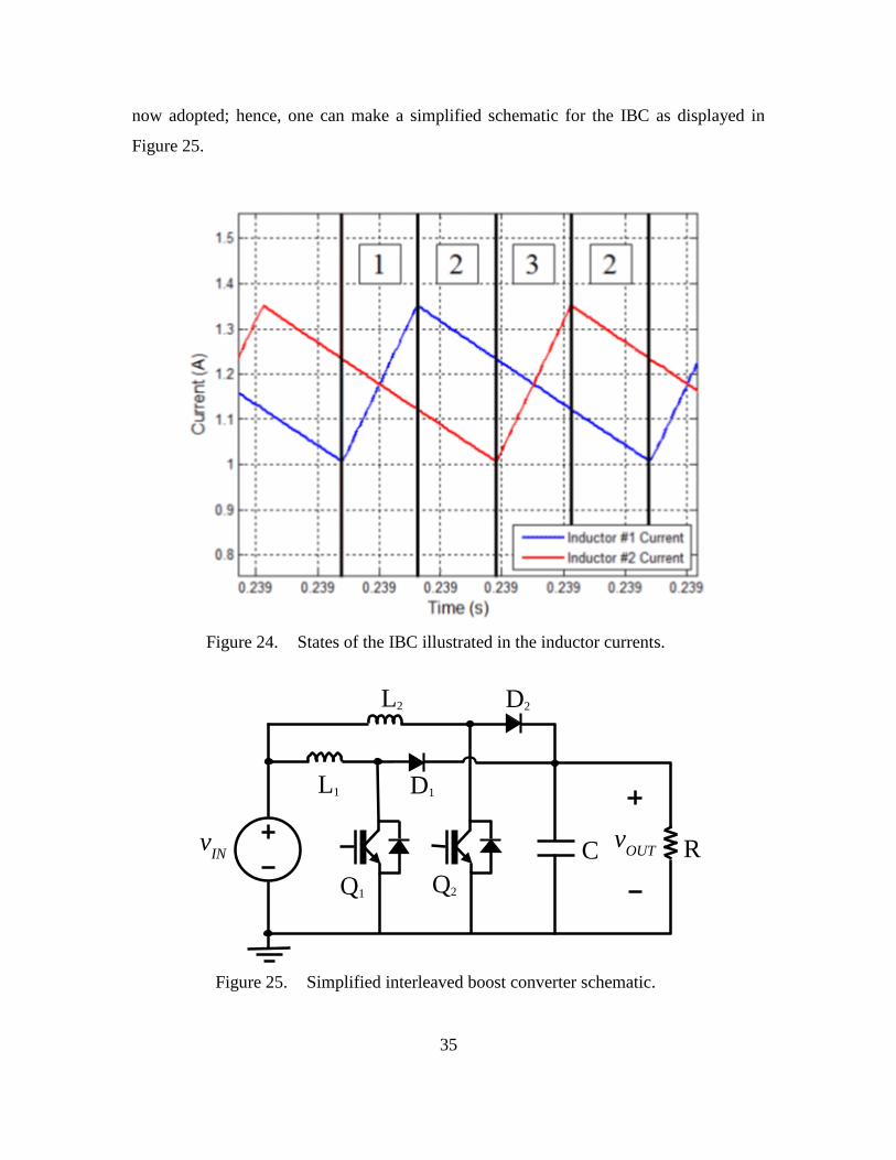
35
now adopted; hence, one can make a simplified schematic for the IBC as displayed in
Figure 25.
States of the IBC illustrated in the inductor currents. Figure 24.
Simplified interleaved boost converter schematic. Figure 25.
R v
OUT
L2
vIN
Q2
D2
L1 D1
C
Q1
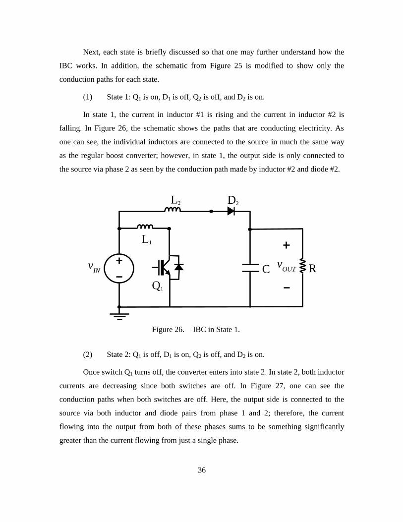
36
Next, each state is briefly discussed so that one may further understand how the
IBC works. In addition, the schematic from Figure 25 is modified to show only the
conduction paths for each state.
(1) State 1: Q1 is on, D1 is off, Q2 is off, and D2 is on.
In state 1, the current in inductor #1 is rising and the current in inductor #2 is
falling. In Figure 26, the schematic shows the paths that are conducting electricity. As
one can see, the individual inductors are connected to the source in much the same way
as the regular boost converter; however, in state 1, the output side is only connected to
the source via phase 2 as seen by the conduction path made by inductor #2 and diode #2.
IBC in State 1. Figure 26.
(2) State 2: Q1 is off, D1 is on, Q2 is off, and D2 is on.
Once switch Q1 turns off, the converter enters into state 2. In state 2, both inductor
currents are decreasing since both switches are off. In Figure 27, one can see the
conduction paths when both switches are off. Here, the output side is connected to the
source via both inductor and diode pairs from phase 1 and 2; therefore, the current
flowing into the output from both of these phases sums to be something significantly
greater than the current flowing from just a single phase.
R v
OUT
L2
vIN
D2
L1
C
Q1
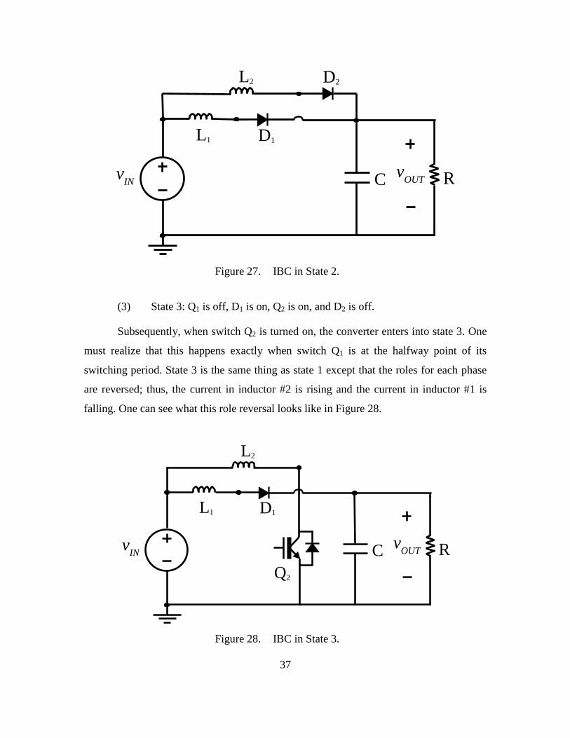
37
IBC in State 2. Figure 27.
(3) State 3: Q1 is off, D1 is on, Q2 is on, and D2 is off.
Subsequently, when switch Q2 is turned on, the converter enters into state 3. One
must realize that this happens exactly when switch Q1 is at the halfway point of its
switching period. State 3 is the same thing as state 1 except that the roles for each phase
are reversed; thus, the current in inductor #2 is rising and the current in inductor #1 is
falling. One can see what this role reversal looks like in Figure 28.
IBC in State 3. Figure 28.
R v
OUT
L2
vIN
D2
L1 D1
C
R v
OUT
L2
vIN
Q2
L1 D1
C
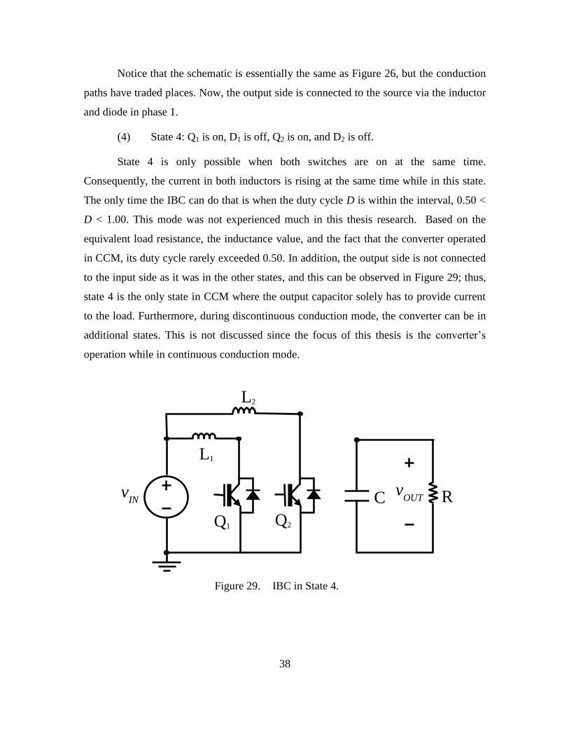
38
Notice that the schematic is essentially the same as Figure 26, but the conduction
paths have traded places. Now, the output side is connected to the source via the inductor
and diode in phase 1.
(4) State 4: Q1 is on, D1 is off, Q2 is on, and D2 is off.
State 4 is only possible when both switches are on at the same time.
Consequently, the current in both inductors is rising at the same time while in this state.
The only time the IBC can do that is when the duty cycle D is within the interval, 0.50 <
D < 1.00. This mode was not experienced much in this thesis research. Based on the
equivalent load resistance, the inductance value, and the fact that the converter operated
in CCM, its duty cycle rarely exceeded 0.50. In addition, the output side is not connected
to the input side as it was in the other states, and this can be observed in Figure 29; thus,
state 4 is the only state in CCM where the output capacitor solely has to provide current
to the load. Furthermore, during discontinuous conduction mode, the converter can be in
additional states. This is not discussed since the focus of this thesis is the converter’s
operation while in continuous conduction mode.
IBC in State 4. Figure 29.
R v
OUT
L2
vIN
Q2
L1
C
Q1
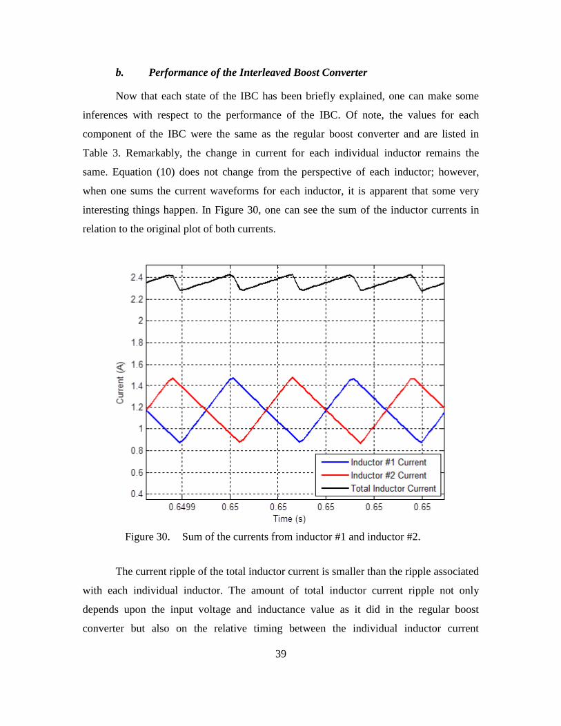
39
b. Performance of the Interleaved Boost Converter
Now that each state of the IBC has been briefly explained, one can make some
inferences with respect to the performance of the IBC. Of note, the values for each
component of the IBC were the same as the regular boost converter and are listed in
Table 3. Remarkably, the change in current for each individual inductor remains the
same. Equation (10) does not change from the perspective of each inductor; however,
when one sums the current waveforms for each inductor, it is apparent that some very
interesting things happen. In Figure 30, one can see the sum of the inductor currents in
relation to the original plot of both currents.
Sum of the currents from inductor #1 and inductor #2. Figure 30.
The current ripple of the total inductor current is smaller than the ripple associated
with each individual inductor. The amount of total inductor current ripple not only
depends upon the input voltage and inductance value as it did in the regular boost
converter but also on the relative timing between the individual inductor current
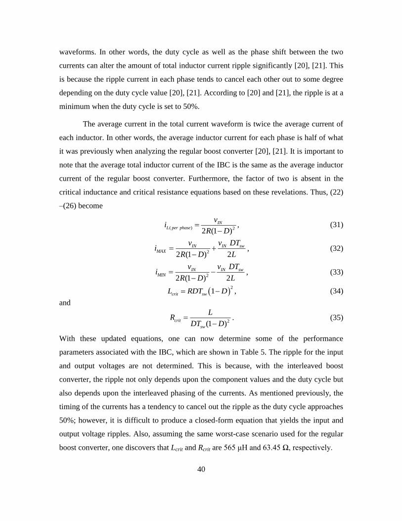
40
waveforms. In other words, the duty cycle as well as the phase shift between the two
currents can alter the amount of total inductor current ripple significantly [20], [21]. This
is because the ripple current in each phase tends to cancel each other out to some degree
depending on the duty cycle value [20], [21]. According to [20] and [21], the ripple is at a
minimum when the duty cycle is set to 50%.
The average current in the total current waveform is twice the average current of
each inductor. In other words, the average inductor current for each phase is half of what
it was previously when analyzing the regular boost converter [20], [21]. It is important to
note that the average total inductor current of the IBC is the same as the average inductor
current of the regular boost converter. Furthermore, the factor of two is absent in the
critical inductance and critical resistance equations based on these revelations. Thus, (22)
–(26) become
( ) 22 (1 )
INL per phase
vi
R D
, (31)
22 (1 ) 2
IN IN swMAX
v v DTi
R D L
, (32)
22 (1 ) 2
IN IN swMIN
v v DTi
R D L
, (33)
2
1crit swL RDT D , (34)
and
2(1 )
crit
sw
LR
DT D
. (35)
With these updated equations, one can now determine some of the performance
parameters associated with the IBC, which are shown in Table 5. The ripple for the input
and output voltages are not determined. This is because, with the interleaved boost
converter, the ripple not only depends upon the component values and the duty cycle but
also depends upon the interleaved phasing of the currents. As mentioned previously, the
timing of the currents has a tendency to cancel out the ripple as the duty cycle approaches
50%; however, it is difficult to produce a closed-form equation that yields the input and
output voltage ripples. Also, assuming the same worst-case scenario used for the regular
boost converter, one discovers that Lcrit and Rcrit are 565 μH and 63.45 Ω, respectively.

41
Table 5. Theoretical Performance Parameters for the IBC.
Parameter Symbol Value
Ripple in inductor current ΔiL 594.4 mA
Ripple in output voltage ΔvOUT Not determined
Ripple in input voltage ΔvIN Not determined
Average inductor current iL(per phase) 1.182 A
Maximum inductor current iMAX 1.479 A
Minimum inductor current iMIN 0.885 A
c. Benefits of the IBC
So far, some of the attributes of the interleaved boost converter have been
explained in detail. In this section, the advantages of the IBC are highlighted further.
Theoretically, the IBC is more efficient since it has fewer conduction losses as compared
to a single boost converter; however, the losses due to the switching action remain the
same. To understand why this is, first, examine Figure 31, which illustrates the concept of
switching losses. Based on Figure 31, the power losses due to switching is characterized
by
( ) ( )
1
2sw off on sw on sw off swP V I t t f , (36)
where Ion is the average current conducting through the switch when it is on, and Voff is
the average voltage across the switch when it is turned off [17], [18]. The symbols tsw(on)
and tsw(off) are the time it takes to turn the switch on and the time it takes to turn the switch
off, respectively [17]. This equation can be extended to the switching action across either
the transistor or the diode, but one must realize that the values used in the equation will
be somewhat different since one is dealing with different components. If one thinks about
the switching losses across one single switch in the IBC, one realizes that the average
current is half of what it was in the regular boost converter; thus, the switching losses
associated with that particular switch are also cut in half. In the IBC, there is twice the
number of switching components as compared to the regular boost converter; therefore,
while the switching losses of a single component are half of what they are in the regular
boost converter, the total switching losses remain the same.
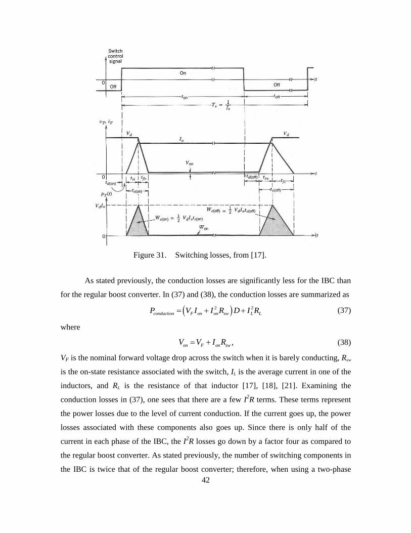
42
Switching losses, from [17]. Figure 31.
As stated previously, the conduction losses are significantly less for the IBC than
for the regular boost converter. In (37) and (38), the conduction losses are summarized as
2 2
conduction F on on sw L LP V I I R D I R (37)
where
on F on swV V I R , (38)
VF is the nominal forward voltage drop across the switch when it is barely conducting, Rsw
is the on-state resistance associated with the switch, IL is the average current in one of the
inductors, and RL is the resistance of that inductor [17], [18], [21]. Examining the
conduction losses in (37), one sees that there are a few I2R terms. These terms represent
the power losses due to the level of current conduction. If the current goes up, the power
losses associated with these components also goes up. Since there is only half of the
current in each phase of the IBC, the I2R losses go down by a factor four as compared to
the regular boost converter. As stated previously, the number of switching components in
the IBC is twice that of the regular boost converter; therefore, when using a two-phase
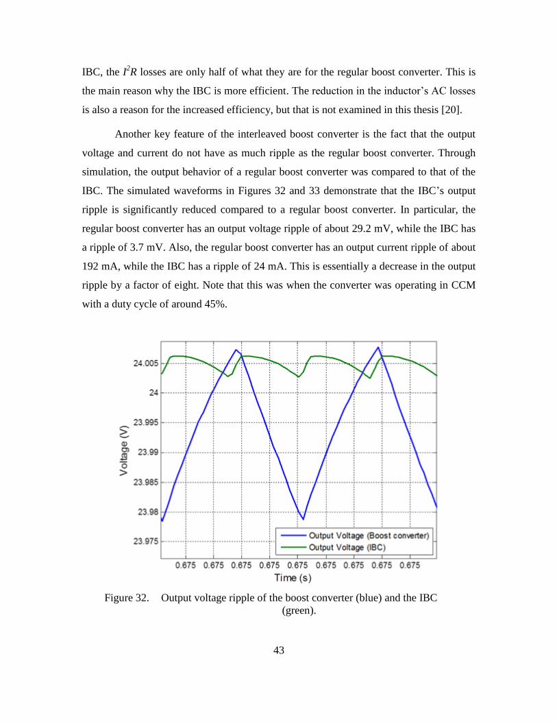
43
IBC, the I2R losses are only half of what they are for the regular boost converter. This is
the main reason why the IBC is more efficient. The reduction in the inductor’s AC losses
is also a reason for the increased efficiency, but that is not examined in this thesis [20].
Another key feature of the interleaved boost converter is the fact that the output
voltage and current do not have as much ripple as the regular boost converter. Through
simulation, the output behavior of a regular boost converter was compared to that of the
IBC. The simulated waveforms in Figures 32 and 33 demonstrate that the IBC’s output
ripple is significantly reduced compared to a regular boost converter. In particular, the
regular boost converter has an output voltage ripple of about 29.2 mV, while the IBC has
a ripple of 3.7 mV. Also, the regular boost converter has an output current ripple of about
192 mA, while the IBC has a ripple of 24 mA. This is essentially a decrease in the output
ripple by a factor of eight. Note that this was when the converter was operating in CCM
with a duty cycle of around 45%.
Output voltage ripple of the boost converter (blue) and the IBC Figure 32.
(green).
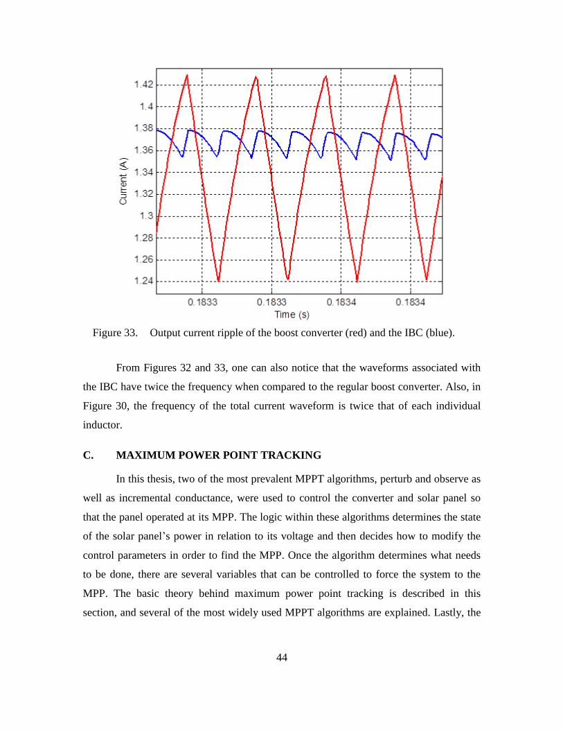
44
Output current ripple of the boost converter (red) and the IBC (blue). Figure 33.
From Figures 32 and 33, one can also notice that the waveforms associated with
the IBC have twice the frequency when compared to the regular boost converter. Also, in
Figure 30, the frequency of the total current waveform is twice that of each individual
inductor.
C. MAXIMUM POWER POINT TRACKING
In this thesis, two of the most prevalent MPPT algorithms, perturb and observe as
well as incremental conductance, were used to control the converter and solar panel so
that the panel operated at its MPP. The logic within these algorithms determines the state
of the solar panel’s power in relation to its voltage and then decides how to modify the
control parameters in order to find the MPP. Once the algorithm determines what needs
to be done, there are several variables that can be controlled to force the system to the
MPP. The basic theory behind maximum power point tracking is described in this
section, and several of the most widely used MPPT algorithms are explained. Lastly, the

45
different ways a power converter’s duty cycle can be modified in order to implement
these algorithms is discussed.
1. Perturb and Observe
Perturb and observe is probably the most commonly utilized MPPT method [24].
The basic premise for P&O is to continually perturb or alter the power converter’s
operating point and then to observe or sense the ensuing effects. In other words, the
settings within the converter are changed so that the solar panel’s voltage and current are
changed. Then, the system senses the panel’s voltage and current to see if its power has
increased or decreased. Subsequently, the algorithm makes a decision on how to further
adjust the converter’s settings. Typically, the settings that are modified are either a
reference voltage or the duty cycle. A reference current may also be used, but this method
is less common for reasons that are explained later.
In Figure 34, the P&O flowchart is presented in order to understand the finer
details of this algorithm. As one can see from Figure 34, the algorithm reads in the
voltage measurements V[k] and the current measurements I[k] at a specified time interval
called the MPPT period. This time interval governs how often the algorithm makes a
decision to change the operating point of the system. Subsequently, the algorithm
calculates the power P[k], the change in power ΔP, and the change in voltage ΔV. The ΔP
and ΔV values are found by using the measurements at the present moment V[k] and I[k]
as well as the previous measurements V[k-1] and I[k-1]. From there, the algorithm uses
basic logic in order to decide what to do. The ΔP and ΔV values are each compared
against zero to determine if they have increased or decreased. Next, if one uses an XNOR
logic gate, this decision is relatively simple as shown in Table 6. Here, a “0” constitutes a
false answer to the logic, while a “1” represents a true answer. For example, in the input
columns of Table 6, a “0” means that the quantity has decreased and a “1” means that the
quantity has increased. The output column is the logical result of the XNOR gate, and
this is used to drive either the duty cycle or the reference voltage according to the
algorithm. To summarize, if the power goes up after a certain perturbation, then the next
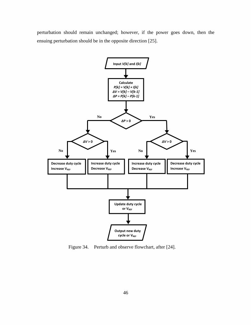
46
perturbation should remain unchanged; however, if the power goes down, then the
ensuing perturbation should be in the opposite direction [25].
Perturb and observe flowchart, after [24]. Figure 34.
Calculate P[k] = V[k] × I[k] ΔV = V[k] – V[k-1] ΔP = P[k] – P[k-1]
Input V[k] and I[k]
Decrease duty cycle
Increase VREF
Decrease duty cycle
Increase VREF
Update duty cycle or VREF
ΔP > 0
ΔV > 0
Increase duty cycle
Decrease VREF
Increase duty cycle
Decrease VREF
Output new duty cycle or VREF
Yes
Yes Yes No No
No
ΔV > 0
47
Table 6. XNOR logic used in the P&O algorithm.
Input Output Results
ΔP > 0 ΔV ≥ 0 ΔP > 0 XNOR ΔV ≥ 0 Duty Cycle Reference Voltage
0 0 1 Decrease Increase
0 1 0 Increase Decrease
1 0 0 Increase Decrease
1 1 1 Decrease Increase
Utilizing the P&O algorithm has several benefits. For one, it is a reliable approach
to MPPT, which means that it finds the MPP in almost all circumstances. Also, it is
relatively simple and easy to implement [25]. Additionally, it does not require a lot of
logic or computational calculations when compared to other methods; however, it does
require two sensors – one for the voltage and one for the current [25]. On the other hand,
there are a few shortcomings of the P&O MPPT method. For one, this MPPT algorithm
always oscillates about the maximum power point and is never truly stable at the MPP
[22], [25], [26]. This may result in a reduced amount of power that can be generated by
the system [22], [26].
Furthermore, P&O may command the wrong perturbation during rapidly changing
solar irradiance conditions. As explained in detail by [25] and [26], the algorithm may
decide to command the opposite of what should be done. Consider the situation where the
solar irradiance is at 800 W/m2 and the system is very close to the MPP as depicted at
point A in Figure 35. Due to the nature of P&O, the algorithm commands a perturbation
even though it is very close to the MPP. Suppose that its command causes the voltage to
increase to point B, assuming the solar irradiance stayed the same. Consequently, the
algorithm would correctly decide to reduce the voltage since the power decreased when
the voltage was increased. Now consider a different scenario. This set of circumstances
starts out exactly the same as the first situation. The algorithm decides to perturb the
system away from the MPP, which results with an increase in voltage. Assume the solar
irradiance rapidly increases to 1000 W/m2 prior to the next MPPT decision. This causes
the algorithm to sense that both the power and the voltage have increased, as is shown by
the transition from point A to point C. Consequently, the algorithm commands the system
to increase the voltage. As one can see in Figure 35, this is not what should be done to
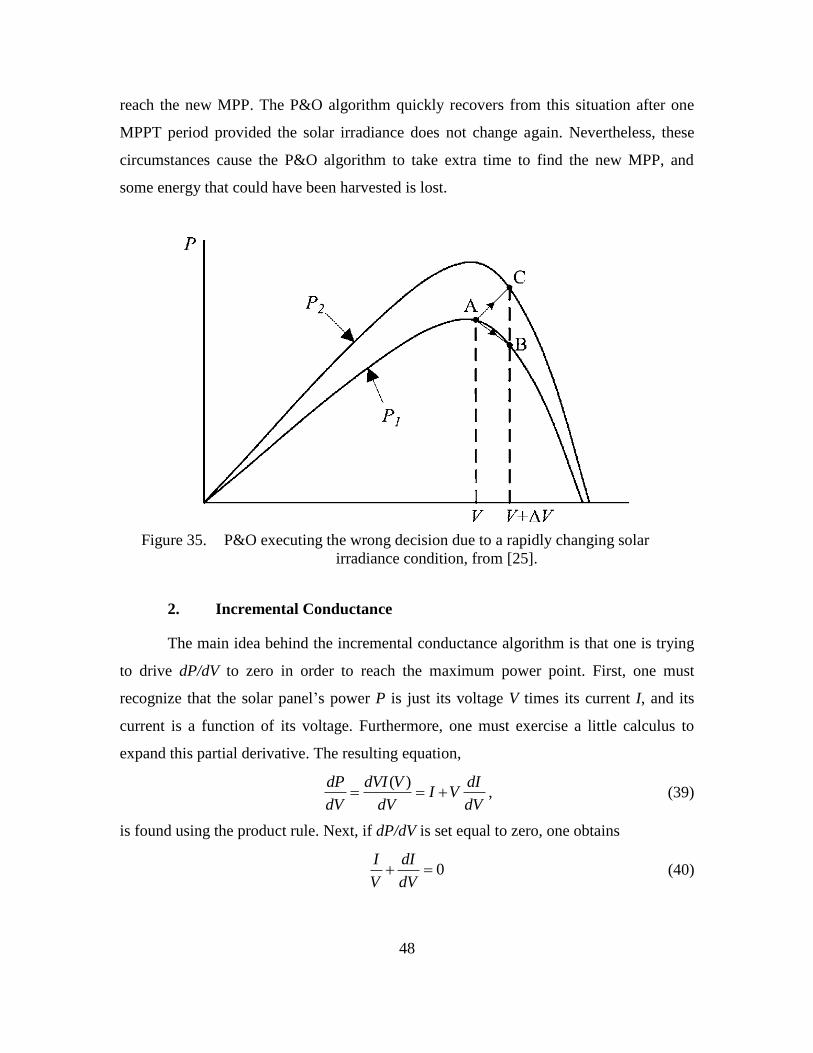
48
reach the new MPP. The P&O algorithm quickly recovers from this situation after one
MPPT period provided the solar irradiance does not change again. Nevertheless, these
circumstances cause the P&O algorithm to take extra time to find the new MPP, and
some energy that could have been harvested is lost.
P&O executing the wrong decision due to a rapidly changing solar Figure 35.
irradiance condition, from [25].
2. Incremental Conductance
The main idea behind the incremental conductance algorithm is that one is trying
to drive dP/dV to zero in order to reach the maximum power point. First, one must
recognize that the solar panel’s power P is just its voltage V times its current I, and its
current is a function of its voltage. Furthermore, one must exercise a little calculus to
expand this partial derivative. The resulting equation,
( )dP dVI V dI
I VdV dV dV
, (39)
is found using the product rule. Next, if dP/dV is set equal to zero, one obtains
0I dI
V dV (40)
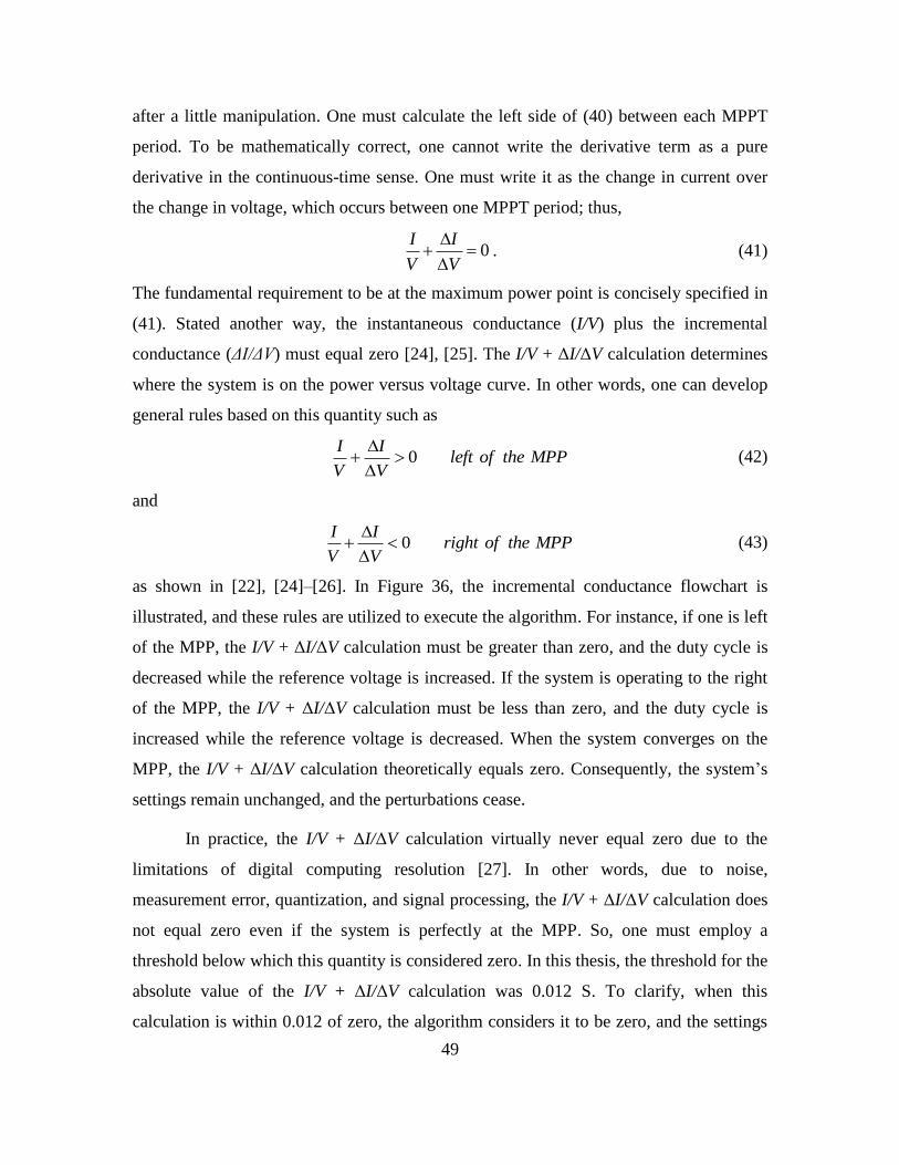
49
after a little manipulation. One must calculate the left side of (40) between each MPPT
period. To be mathematically correct, one cannot write the derivative term as a pure
derivative in the continuous-time sense. One must write it as the change in current over
the change in voltage, which occurs between one MPPT period; thus,
0I I
V V
. (41)
The fundamental requirement to be at the maximum power point is concisely specified in
(41). Stated another way, the instantaneous conductance (I/V) plus the incremental
conductance (ΔI/ΔV) must equal zero [24], [25]. The I/V + ΔI/ΔV calculation determines
where the system is on the power versus voltage curve. In other words, one can develop
general rules based on this quantity such as
0I I
left of the MPPV V
(42)
and
0I I
right of the MPPV V
(43)
as shown in [22], [24]–[26]. In Figure 36, the incremental conductance flowchart is
illustrated, and these rules are utilized to execute the algorithm. For instance, if one is left
of the MPP, the I/V + ΔI/ΔV calculation must be greater than zero, and the duty cycle is
decreased while the reference voltage is increased. If the system is operating to the right
of the MPP, the I/V + ΔI/ΔV calculation must be less than zero, and the duty cycle is
increased while the reference voltage is decreased. When the system converges on the
MPP, the I/V + ΔI/ΔV calculation theoretically equals zero. Consequently, the system’s
settings remain unchanged, and the perturbations cease.
In practice, the I/V + ΔI/ΔV calculation virtually never equal zero due to the
limitations of digital computing resolution [27]. In other words, due to noise,
measurement error, quantization, and signal processing, the I/V + ΔI/ΔV calculation does
not equal zero even if the system is perfectly at the MPP. So, one must employ a
threshold below which this quantity is considered zero. In this thesis, the threshold for the
absolute value of the I/V + ΔI/ΔV calculation was 0.012 S. To clarify, when this
calculation is within 0.012 of zero, the algorithm considers it to be zero, and the settings

50
are not changed. Furthermore, the system is so close to the MPP at this point that it is
completely reasonable to stop perturbing the system.
Once the I/V + ΔI/ΔV calculation is within the threshold, the algorithm commands
the system to stop changing the voltage and current for one MPPT period. If after that
MPPT period the algorithm determines that the ΔV and ΔI are both zero, then the
algorithm keeps the system operating at that point. Practically, ΔV or ΔI is never exactly
zero for the reasons mentioned earlier. When determining if ΔV or ΔI is equal to zero, it
is necessary to utilize another threshold. This threshold is a small value that is sufficiently
close to zero but allows for small deviations due to noise and measurement errors. In this
thesis, the thresholds for ΔV and ΔI were set to 0.007 V and 0.006 A, respectively. When
ΔV is less than 0.007 V and ΔI is also less than 0.006 A, the algorithm does not change
the duty cycle. Unless either the ΔV or the ΔI subsequently changes enough to exceed
their thresholds, the system is locked at the MPP.
Additionally, when the ΔV is close to zero, then the I/V + ΔI/ΔV calculation may
be abnormally large. Typically, this occurs when ΔI is also small but slightly larger in
magnitude than ΔV due to noise; however, faulty calculations can take place in other
circumstances. For instance, erroneous calculations may take place due to biases in the
measurements. The bottom line is that this can cause some problems for the control
algorithm; hence, it is necessary to offer a logical alternative in this case. That is why the
algorithm first asks if ΔV equals zero. If ΔV is large enough, then the I/V + ΔI/ΔV
calculation is used to find the MPP. If ΔV is small enough to be considered zero, then the
alternate logic path is taken. Then the algorithm checks if ΔI is close enough to zero. If it
is, the system does not change its settings. If ΔI exceeds its threshold due to a change in
irradiance or random noise, then the system is perturbed according to the ΔI > 0 logic.
Primarily, the alternate logic path exists to account for changing irradiance levels
when the ΔV does not exceed its threshold. Referencing Figure 37, one can visualize
what happens with respect to the power versus voltage curve in this situation. If the
irradiance level goes up while the voltage does not change, the current and the power
increase; however, on this new power versus voltage curve, the system is now left of the
MPP, and the algorithm is programmed to increase the reference voltage (or decrease
51
duty cycle). A similar argument can be made for when the irradiance decreases in order
to determine what the IC algorithm decides to do. In this case, it decreases the reference
voltage (or increases the duty cycle).
Incremental conductance flowchart, after [24] and [25]. Figure 36.
Calculate
ΔV = V[k] – V[k-1] ΔI = I[k] – I[k-1] ΔI/ΔV + I/V
Input V[k] and I[k]
Decrease duty cycle
Increase VREF
Decrease duty cycle
Increase VREF
Update duty cycle or VREF
ΔV = 0
ΔI = 0
ΔI > 0
Increase duty cycle
Decrease VREF
Increase duty cycle
Decrease VREF
ΔI/ΔV + I/V = 0
ΔI/ΔV + I/V > 0
Output new duty cycle or VREF
Yes
Yes Yes
Yes Yes No No
No No
No
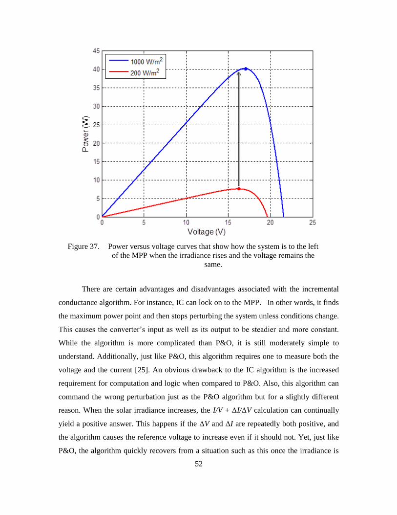
52
Power versus voltage curves that show how the system is to the left Figure 37.
of the MPP when the irradiance rises and the voltage remains the
same.
There are certain advantages and disadvantages associated with the incremental
conductance algorithm. For instance, IC can lock on to the MPP. In other words, it finds
the maximum power point and then stops perturbing the system unless conditions change.
This causes the converter’s input as well as its output to be steadier and more constant.
While the algorithm is more complicated than P&O, it is still moderately simple to
understand. Additionally, just like P&O, this algorithm requires one to measure both the
voltage and the current [25]. An obvious drawback to the IC algorithm is the increased
requirement for computation and logic when compared to P&O. Also, this algorithm can
command the wrong perturbation just as the P&O algorithm but for a slightly different
reason. When the solar irradiance increases, the I/V + ΔI/ΔV calculation can continually
yield a positive answer. This happens if the ΔV and ΔI are repeatedly both positive, and
the algorithm causes the reference voltage to increase even if it should not. Yet, just like
P&O, the algorithm quickly recovers from a situation such as this once the irradiance is

53
relatively stable. On the other hand, when the solar irradiance decreases, the I/V + ΔI/ΔV
computation tends to alternate between a positive and negative value, and the algorithm
essentially keeps the reference voltage where it was prior to the decrease in irradiance. As
a final point, IC can possibly lock onto the wrong setting. If an erroneous I/V + ΔI/ΔV
calculation causes the algorithm to command no change in the duty cycle, then the
algorithm may detect ΔV and ΔI below their thresholds after the next MPPT period. This
causes the algorithm to stay at the current operating point indefinitely even if it is not the
MPP. Either a change in irradiance or excessive noise in the current or voltage signal may
cause the algorithm to exit this adverse mode of operation.
3. Other MPPT Methods
There are many other MPPT methods employed, and they are chronicled in the
literature. In [4] and [22], many of these techniques are discussed. In this section of this
thesis, some of these methods are explained.
(1) Constant Duty Cycle or Constant Reference Voltage
One of the simplest means of controlling a solar module is to select a constant
duty cycle that drives the solar module’s voltage close enough to the MPP. Since the duty
ratio does not change, there is nothing to alter; thus, it does not require any measurements
or feedback [27]. Alternatively, one can select a constant reference voltage. Here, the
solar panel’s voltage must be measured in order to drive it towards the preselected
reference voltage [22], [26]. Both of these methods assume that changing temperature
and irradiance conditions are not relevant and can be ignored [22], [26]. Even though
these techniques are simple, they do not track the MPP but merely get the panel’s output
close enough to the MPP so that most of the power available can be harvested. It must be
noted that, at low levels of irradiance, these methods may prove to be better than any
other [22], [26].
(2) Open-Circuit Voltage or Short-Circuit Current
Another simple, yet sometimes inaccurate, way to control a solar module is to
measure either the open-circuit voltage, short-circuit current, or both. The voltage at the
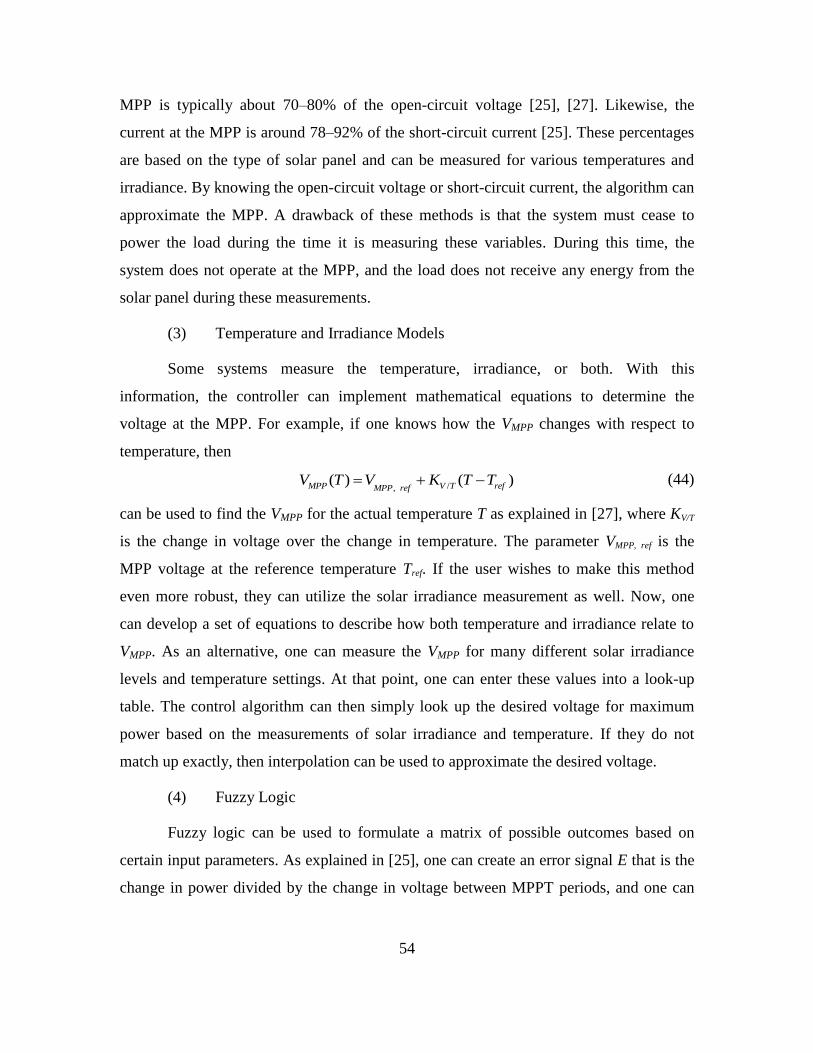
54
MPP is typically about 70–80% of the open-circuit voltage [25], [27]. Likewise, the
current at the MPP is around 78–92% of the short-circuit current [25]. These percentages
are based on the type of solar panel and can be measured for various temperatures and
irradiance. By knowing the open-circuit voltage or short-circuit current, the algorithm can
approximate the MPP. A drawback of these methods is that the system must cease to
power the load during the time it is measuring these variables. During this time, the
system does not operate at the MPP, and the load does not receive any energy from the
solar panel during these measurements.
(3) Temperature and Irradiance Models
Some systems measure the temperature, irradiance, or both. With this
information, the controller can implement mathematical equations to determine the
voltage at the MPP. For example, if one knows how the VMPP changes with respect to
temperature, then
/,
( ) ( )MPP VMPP ref T refT K TV TV (44)
can be used to find the VMPP for the actual temperature T as explained in [27], where KV/T
is the change in voltage over the change in temperature. The parameter VMPP, ref is the
MPP voltage at the reference temperature Tref. If the user wishes to make this method
even more robust, they can utilize the solar irradiance measurement as well. Now, one
can develop a set of equations to describe how both temperature and irradiance relate to
VMPP. As an alternative, one can measure the VMPP for many different solar irradiance
levels and temperature settings. At that point, one can enter these values into a look-up
table. The control algorithm can then simply look up the desired voltage for maximum
power based on the measurements of solar irradiance and temperature. If they do not
match up exactly, then interpolation can be used to approximate the desired voltage.
(4) Fuzzy Logic
Fuzzy logic can be used to formulate a matrix of possible outcomes based on
certain input parameters. As explained in [25], one can create an error signal E that is the
change in power divided by the change in voltage between MPPT periods, and one can

55
calculate the change in this error signal ΔE. As presented in [25], an example of these
calculations is
[ ] [ 1]
[ ][ ] [ 1]
P k P kE k
V k V k
(45)
and
[ ] [ 1]E E k E k . (46)
With these calculations, one can proceed to the next step, which is to categorize these
inputs using a fuzzy logic table as depicted in Figure 38.
NB NS ZE PS PB
NB ZE ZE NB NB NB
NS ZE ZE NS NS NS
ZE NS ZE ZE ZE PS
PS PS PS PS ZE ZE
PB PB PB PB ZE ZE
An example of a fuzzy logic table, from [25]. Figure 38.
In Figure 38, NB is negative big, NS is negative small, ZE is zero, PS is positive
small, and PB is positive big [25]. The programmer has to decide the numerical
thresholds for defining what constitutes NB vs. NS and so on. Once the algorithm
determines how to categorize the inputs E and ΔE from the look-up table, a change to the
control parameters may be applied. For instance, PB may mean that a 2% change in duty
cycle ΔD is warranted, while PS may mean that only a 1% increment is necessary. If the
fuzzy logic table determines that the inputs fall into the ZE category, then the increment
in duty cycle (or reference voltage) is zero.
(5) Current Sweep
The current sweep method involves systematically varying the current from the
solar panel at certain intervals [25]. By doing this, the controller can take several voltage
E
ΔE

56
and current measurements in order to determine the voltage that produces the MPP [25].
Once this is known, the controller attempts to drive the solar panel’s voltage to the MPP
voltage. The disadvantage of this method is that the system must take time to run the
current sweep. Just like the open-circuit voltage and short-circuit current methods, the
system does not operate at the maximum power point at all times.
(6) Ripple Correlation Control
Ripple Correlation Control is similar to other MPPT methods except one
measures the AC ripple in the panel’s voltage and current. Using this information, one
can correlate the time rate of change of the power p with either the time rate of change of
the voltage v or the current i [25]. As outlined in [25],
( ) RCCd t K pv dt (47)
describes a control law that uses the voltage and power ripple to determine the duty cycle
d(t), where KRCC is a proportionality constant. From (47), one notices that when p and v
are either both positive or both negative, the duty cycle decreases. The result is that when
the panel operates to the left of the MPP, the duty cycle decreases in order to increase the
panel’s voltage. Conversely, when p is positive and v is negative (or vice versa), the
duty cycle increases. In this case, the panel operates to the right of the MPP, and the duty
cycle increases in order to decrease the panel’s voltage.
(7) dP/dV or dP/dI
A more intuitive way of controlling the panel is to calculate a partial derivative,
either dP/dV or dP/dI. It is important to note that these derivatives are simply the slope of
the power versus voltage curve or the power versus current curve, respectively. One can
see from those plots that the MPP occurs when the slope equals zero. By using this
method, one can drive the partial derivative to zero and reach the MPPT [25].
(8) Maximize Output Current or Voltage
Still another method of MPPT is to maximize either the output current or output
voltage. By doing this, the converter also maximizes the input power from the solar
panel. As explained in [28], the load can be voltage-source type, current-source type,

57
resistive-type, or a combination. In this thesis, the output is voltage-source type due to the
inclusion of a battery in the circuit; thus, one can attempt to maximize the output current
and arrive at the MPP. An advantage of this type of control methodology is that only one
sensor is required [25].
(9) IC or dP/dV by Proportional-Integral Control
There is yet another method for conducting MPPT that involves using a
proportional-integral (PI) controller [25], [27]. Here, the I/V + ΔI/ΔV is calculated just as
in the IC method. This calculation is subtracted from a reference value of zero, and this
error signal is then fed into a PI controller to drive the error to zero [25]. This same
method can be used for the dP/dV calculation. Note that the output from the PI controller
is the duty cycle value as depicted in [27].
D. METHODS OF CONTROLLING DUTY CYCLE
How the controller calculates where the system is with respect to the MPP and
how, at that moment, it decides to adjust the duty cycle (increase, decrease, or neither) in
order to track the MPP was explained in the previous section. The various ways the duty
cycle can be realized once the MPPT algorithm makes a decision is described in this
section.
1. Direct Duty Cycle Control
The most straightforward way to adjust the duty cycle in response to the
command given from the MPPT algorithm is control it directly. Using this method of
control involves simply incrementing or decrementing the duty cycle in order to find the
MPP; however, there is an opposite correlation between the input voltage, which is solar
panel’s voltage, and the duty cycle. For instance, the input voltage decreases while the
duty cycle increases and vice versa. To understand why this is so, one must first recall the
input and output relationship for the voltages of a boost converter from (17), which can
be transformed to yield
1 IN
OUT
vD
v . (48)
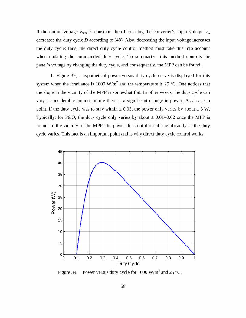
58
If the output voltage vOUT is constant, then increasing the converter’s input voltage vIN
decreases the duty cycle D according to (48). Also, decreasing the input voltage increases
the duty cycle; thus, the direct duty cycle control method must take this into account
when updating the commanded duty cycle. To summarize, this method controls the
panel’s voltage by changing the duty cycle, and consequently, the MPP can be found.
In Figure 39, a hypothetical power versus duty cycle curve is displayed for this
system when the irradiance is 1000 W/m2 and the temperature is 25 °C. One notices that
the slope in the vicinity of the MPP is somewhat flat. In other words, the duty cycle can
vary a considerable amount before there is a significant change in power. As a case in
point, if the duty cycle was to stay within ± 0.05, the power only varies by about ± 3 W.
Typically, for P&O, the duty cycle only varies by about ± 0.01–0.02 once the MPP is
found. In the vicinity of the MPP, the power does not drop off significantly as the duty
cycle varies. This fact is an important point and is why direct duty cycle control works.
Power versus duty cycle for 1000 W/m2 and 25 °C. Figure 39.
0 0.1 0.2 0.3 0.4 0.5 0.6 0.7 0.8 0.9 10
5
10
15
20
25
30
35
40
45
Po
we
r (W
)
Duty Cycle
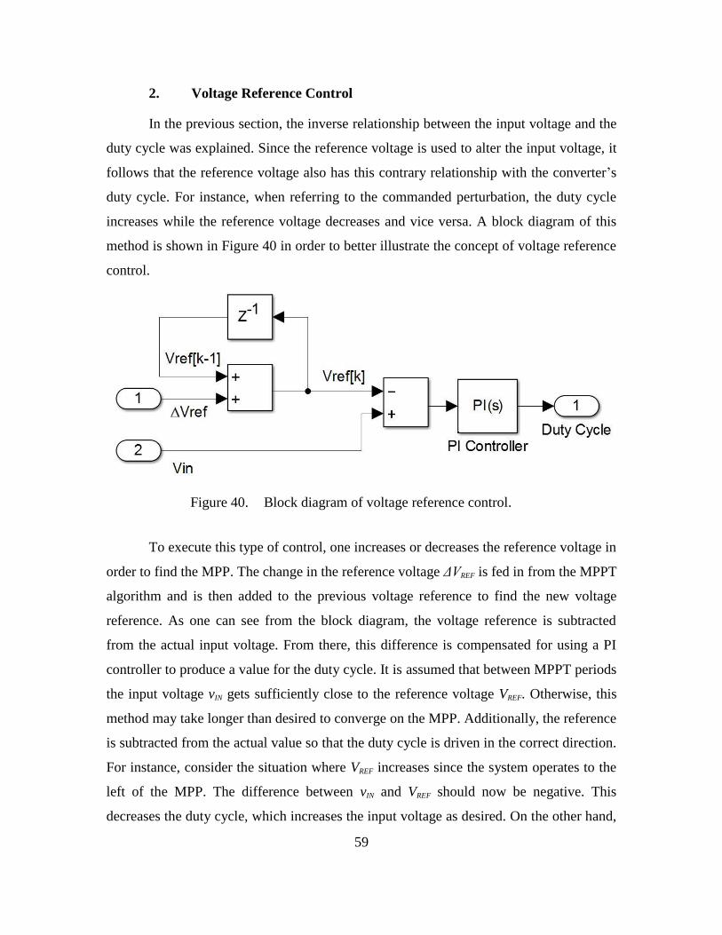
59
2. Voltage Reference Control
In the previous section, the inverse relationship between the input voltage and the
duty cycle was explained. Since the reference voltage is used to alter the input voltage, it
follows that the reference voltage also has this contrary relationship with the converter’s
duty cycle. For instance, when referring to the commanded perturbation, the duty cycle
increases while the reference voltage decreases and vice versa. A block diagram of this
method is shown in Figure 40 in order to better illustrate the concept of voltage reference
control.
Block diagram of voltage reference control. Figure 40.
To execute this type of control, one increases or decreases the reference voltage in
order to find the MPP. The change in the reference voltage ΔVREF is fed in from the MPPT
algorithm and is then added to the previous voltage reference to find the new voltage
reference. As one can see from the block diagram, the voltage reference is subtracted
from the actual input voltage. From there, this difference is compensated for using a PI
controller to produce a value for the duty cycle. It is assumed that between MPPT periods
the input voltage vIN gets sufficiently close to the reference voltage VREF. Otherwise, this
method may take longer than desired to converge on the MPP. Additionally, the reference
is subtracted from the actual value so that the duty cycle is driven in the correct direction.
For instance, consider the situation where VREF increases since the system operates to the
left of the MPP. The difference between vIN and VREF should now be negative. This
decreases the duty cycle, which increases the input voltage as desired. On the other hand,
60
if the system operates to the right of the MPP, the MPPT algorithm commands VREF to
decreases, which creates a positive difference between vIN and VREF. This causes the duty
cycle to rise, and the input voltage goes down.
3. Current Reference Control
Another method that can be used to control the duty cycle is current reference
control. In Figure 41, a block diagram for current reference control is displayed so that
one may understand the subtle differences between voltage reference control and current
reference control. One can see that this method is very similar to voltage reference
control, but the control variable is now current vice voltage. Also, the convention for
finding the difference between the input and the reference is not reversed. In other words,
one subtracts the input current from the reference current to find the difference, which is
fed into the PI controller. The reason for this can be explained rather easily. Normally,
the input current changes in the direction opposite to the input voltage unless there is a
significant change in irradiance; thus, increasing the current requires that the duty cycle
also increases. Conversely, if the current goes down, then the duty cycle should go down
as well.
Block diagram of current reference control. Figure 41.
As alluded to earlier in this thesis, current reference control is not commonly
used. This method has a significant drawback according to [4]. In Figure 42, one will
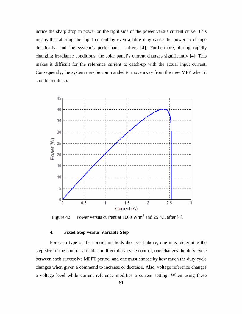
61
notice the sharp drop in power on the right side of the power versus current curve. This
means that altering the input current by even a little may cause the power to change
drastically, and the system’s performance suffers [4]. Furthermore, during rapidly
changing irradiance conditions, the solar panel’s current changes significantly [4]. This
makes it difficult for the reference current to catch-up with the actual input current.
Consequently, the system may be commanded to move away from the new MPP when it
should not do so.
Power versus current at 1000 W/m2 and 25 °C, after [4]. Figure 42.
4. Fixed Step versus Variable Step
For each type of the control methods discussed above, one must determine the
step-size of the control variable. In direct duty cycle control, one changes the duty cycle
between each successive MPPT period, and one must choose by how much the duty cycle
changes when given a command to increase or decrease. Also, voltage reference changes
a voltage level while current reference modifies a current setting. When using these

62
control methods, one must decide by how much to alter the reference setting. One can use
a fixed step-size where the change in duty cycle (or reference level) is constant regardless
of the operating point. For example, one may elect to change the duty cycle by 0.005
every time the algorithm determines a change needs to be made. On the other hand, one
may elect to use a variable step-size. Here, the step-size is varied based on how far away
the operating point is from the MPP. The control parameter’s step-size, in part,
determines the speed of the algorithm. A larger step-size causes the algorithm to
converge on the MPP more quickly than a smaller one, but too large of a step-size may
cause the algorithm to fluctuate around the MPP too much. A variable step-size uses a
larger step when further from the MPP and a smaller step when close to the MPP. The
other component that determines the algorithm’s speed is the frequency of the MPPT
update rate fMPPT, which is the inverse of the MPPT period. When these two parameters
are multiplied together, the time rate of change of the control parameter is the result. As
stated in [27, pg. 1158], “This rate is a parameter that should be adjusted to allow the
balance between faster response and less fluctuation in steady state.”
5. Discrete Step versus Integration
Up to this point, it has been assumed that the change in the control parameter is
handled as a discrete step. In other words, when the MPPT commands a perturbation, the
duty cycle instantaneously changes to the new value without taking on any intermediate
value. This can be called a discrete step-size, but there is another way to implement the
transition to the new value. This procedure involves using an integrator which ramps the
duty cycle up (or down) to the new value over one MPPT period. In this way, the shift to
the new duty cycle is more gradual and smoother than a discrete jump.
E. TYPES OF SYSTEMS USED FOR SOLAR PHOTOVOLTAIC POWER
CONVERSION
The differences between centralized, string, and micro-converter systems are
explained in this portion of this thesis. The advantages and disadvantages of each type of
system are highlighted. In addition, a theoretical example is given to show how a system
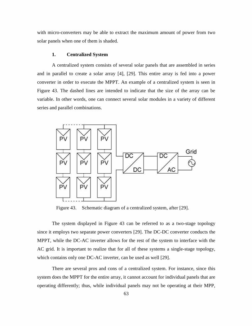
63
with micro-converters may be able to extract the maximum amount of power from two
solar panels when one of them is shaded.
1. Centralized System
A centralized system consists of several solar panels that are assembled in series
and in parallel to create a solar array [4], [29]. This entire array is fed into a power
converter in order to execute the MPPT. An example of a centralized system is seen in
Figure 43. The dashed lines are intended to indicate that the size of the array can be
variable. In other words, one can connect several solar modules in a variety of different
series and parallel combinations.
Schematic diagram of a centralized system, after [29]. Figure 43.
The system displayed in Figure 43 can be referred to as a two-stage topology
since it employs two separate power converters [29]. The DC-DC converter conducts the
MPPT, while the DC-AC inverter allows for the rest of the system to interface with the
AC grid. It is important to realize that for all of these systems a single-stage topology,
which contains only one DC-AC inverter, can be used as well [29].
There are several pros and cons of a centralized system. For instance, since this
system does the MPPT for the entire array, it cannot account for individual panels that are
operating differently; thus, while individual panels may not be operating at their MPP,
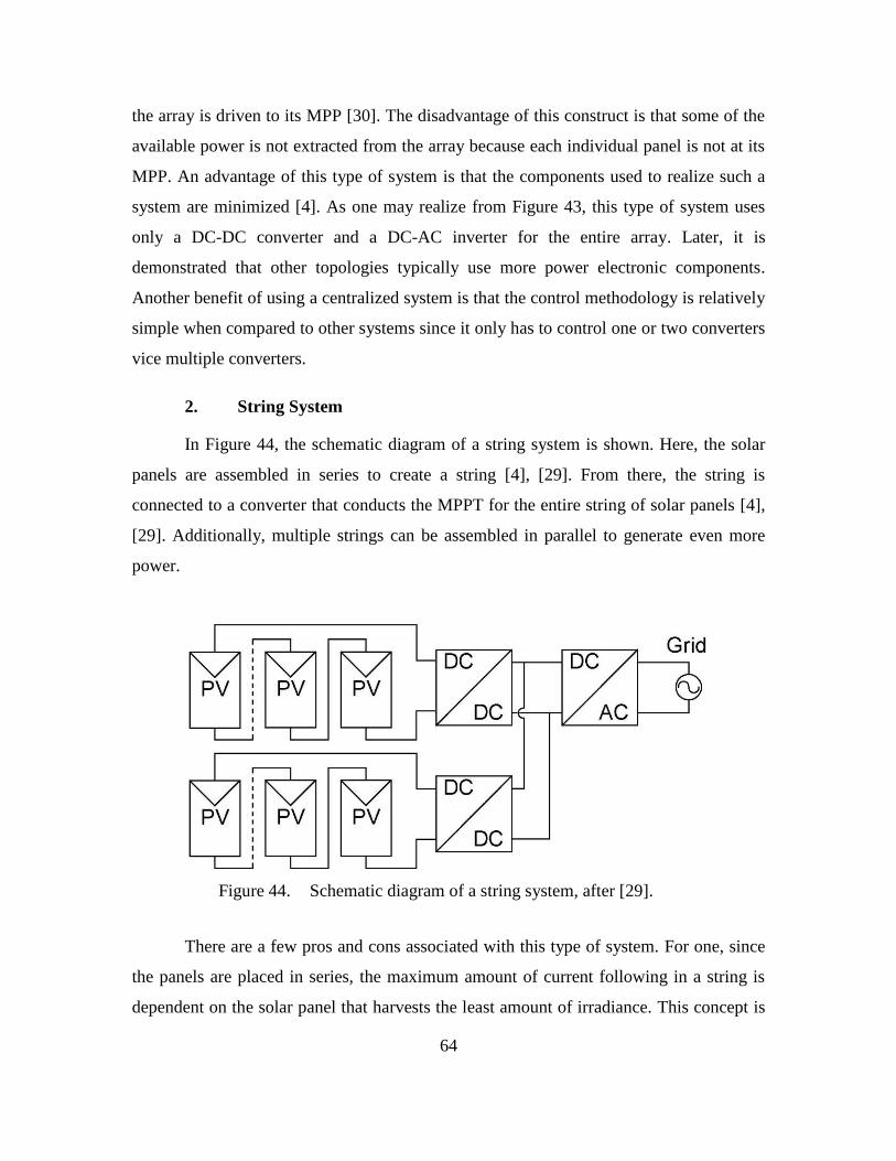
64
the array is driven to its MPP [30]. The disadvantage of this construct is that some of the
available power is not extracted from the array because each individual panel is not at its
MPP. An advantage of this type of system is that the components used to realize such a
system are minimized [4]. As one may realize from Figure 43, this type of system uses
only a DC-DC converter and a DC-AC inverter for the entire array. Later, it is
demonstrated that other topologies typically use more power electronic components.
Another benefit of using a centralized system is that the control methodology is relatively
simple when compared to other systems since it only has to control one or two converters
vice multiple converters.
2. String System
In Figure 44, the schematic diagram of a string system is shown. Here, the solar
panels are assembled in series to create a string [4], [29]. From there, the string is
connected to a converter that conducts the MPPT for the entire string of solar panels [4],
[29]. Additionally, multiple strings can be assembled in parallel to generate even more
power.
Schematic diagram of a string system, after [29]. Figure 44.
There are a few pros and cons associated with this type of system. For one, since
the panels are placed in series, the maximum amount of current following in a string is
dependent on the solar panel that harvests the least amount of irradiance. This concept is

65
developed later in this section, but the main point is that a string system, like the
centralized system, may not produce all of the available power; however, it performs
better than a centralized system [4]. Since a dedicated converter does the MPPT for each
string, the efficiency of power generation is improved when compared to the centralized
system [4], [29]. Another positive aspect of this type of system is that it allows for more
flexibility and modularity [4]. For instance, each string is its own section, which can be
modified or even shutdown without affecting other strings. A disadvantage is that the
number of power electronic components is larger than the number of components for a
centralized system. Additionally, the system has to monitor and control more converters.
3. Micro-converter System
Finally, the micro-converter system, which employs a MPPT converter for each
individual solar panel, is displayed in Figure 45. There are two different schematic
diagrams contained in Figure 45. The one on the left shows a micro-converter system,
where each panel with its own micro-converter is placed in parallel. On the right, each
panel and micro-converter combination is connected in series. Here, only two panels are
shown per diagram. One must realize that it is possible to connect several of these in
series and in parallel to form an entire array made up of many solar panels each with its
own micro-converter.
Schematic diagrams of a micro-converter system in parallel and a Figure 45.
micro-converter system in series, after [29].

66
The advantage of this type of system is that it has the ability to obtain the
maximum power from each solar panel. In addition, if one of the panels is degraded, then
the rest of the system does not suffer [30]. A panel can operate in a degraded state for a
variety of reasons. For instance, it may be old and deteriorated. Also, the module may be
shaded due to debris, snow, trees, or other objects [30]. This type of system epitomizes
flexibility and modularity. For instance, the layout of the system is easily expanded or
reduced without affecting other parts of the system [30]. The micro-converter has some
negative aspects as well. For one, this system, like the string system but more so,
employs several power electronic components. It is important to note that since each
converter interfaces with only one panel, the size of these components can be scaled
down. Furthermore, each panel has a converter that must be controlled, which increases
the complexity.
4. Theoretical Analysis of These Types of Systems
Consider the situation where two solar panels are connected in series. One of the
panels is not shaded and receives 1000 W/m2 from the sun. The other panel is uniformly
shaded such that it effectively experiences just 200 W/m2 of solar irradiance. For this
scenario, the plots of the current versus voltage and the power versus voltage look like
the curves in Figures 46 and 47, respectively. As one can see, the maximum attainable
current is the short-circuit current of the shaded panel. Since the panels are connected in
series, a current mismatch affects the performance of the unshaded panel. In this case, the
resulting power of approximately 16.2 W is significantly lower than the power attainable
from one unshaded panel operating alone. This demonstrates a potential drawback
associated with the centralized and string systems.
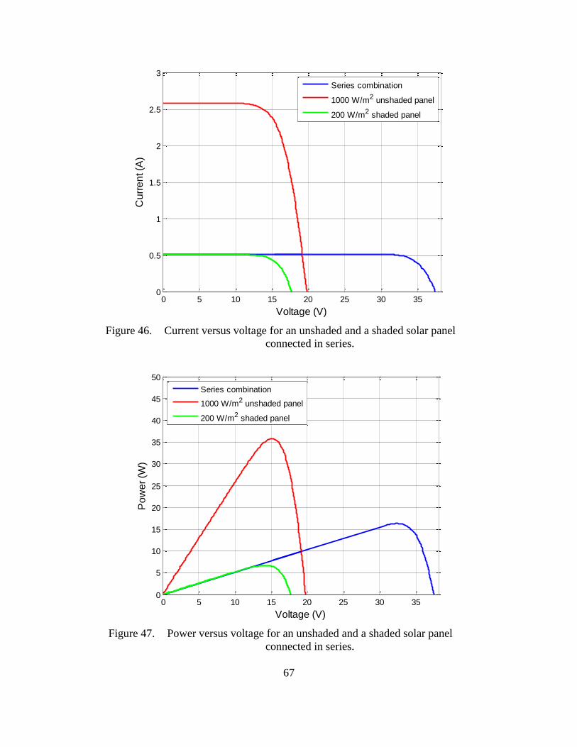
67
Current versus voltage for an unshaded and a shaded solar panel Figure 46.
connected in series.
Power versus voltage for an unshaded and a shaded solar panel Figure 47.
connected in series.
0 5 10 15 20 25 30 350
0.5
1
1.5
2
2.5
3
Voltage (V)
Cu
rre
nt (A
)
Series combination
1000 W/m2 unshaded panel
200 W/m2 shaded panel
0 5 10 15 20 25 30 350
5
10
15
20
25
30
35
40
45
50
Voltage (V)
Po
we
r (W
)
Series combination
1000 W/m2 unshaded panel
200 W/m2 shaded panel
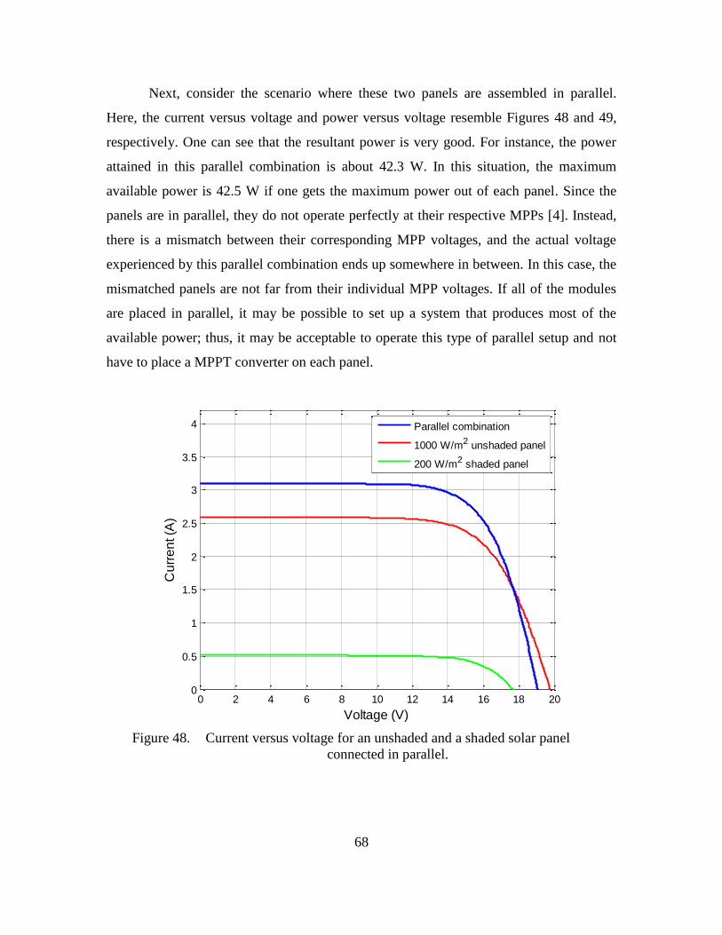
68
Next, consider the scenario where these two panels are assembled in parallel.
Here, the current versus voltage and power versus voltage resemble Figures 48 and 49,
respectively. One can see that the resultant power is very good. For instance, the power
attained in this parallel combination is about 42.3 W. In this situation, the maximum
available power is 42.5 W if one gets the maximum power out of each panel. Since the
panels are in parallel, they do not operate perfectly at their respective MPPs [4]. Instead,
there is a mismatch between their corresponding MPP voltages, and the actual voltage
experienced by this parallel combination ends up somewhere in between. In this case, the
mismatched panels are not far from their individual MPP voltages. If all of the modules
are placed in parallel, it may be possible to set up a system that produces most of the
available power; thus, it may be acceptable to operate this type of parallel setup and not
have to place a MPPT converter on each panel.
Current versus voltage for an unshaded and a shaded solar panel Figure 48.
connected in parallel.
0 2 4 6 8 10 12 14 16 18 200
0.5
1
1.5
2
2.5
3
3.5
4
Voltage (V)
Cu
rre
nt (A
)
Parallel combination
1000 W/m2 unshaded panel
200 W/m2 shaded panel
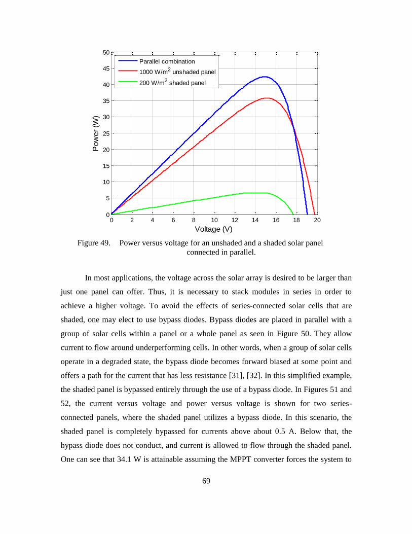
69
Power versus voltage for an unshaded and a shaded solar panel Figure 49.
connected in parallel.
In most applications, the voltage across the solar array is desired to be larger than
just one panel can offer. Thus, it is necessary to stack modules in series in order to
achieve a higher voltage. To avoid the effects of series-connected solar cells that are
shaded, one may elect to use bypass diodes. Bypass diodes are placed in parallel with a
group of solar cells within a panel or a whole panel as seen in Figure 50. They allow
current to flow around underperforming cells. In other words, when a group of solar cells
operate in a degraded state, the bypass diode becomes forward biased at some point and
offers a path for the current that has less resistance [31], [32]. In this simplified example,
the shaded panel is bypassed entirely through the use of a bypass diode. In Figures 51 and
52, the current versus voltage and power versus voltage is shown for two series-
connected panels, where the shaded panel utilizes a bypass diode. In this scenario, the
shaded panel is completely bypassed for currents above about 0.5 A. Below that, the
bypass diode does not conduct, and current is allowed to flow through the shaded panel.
One can see that 34.1 W is attainable assuming the MPPT converter forces the system to
0 2 4 6 8 10 12 14 16 18 200
5
10
15
20
25
30
35
40
45
50
Voltage (V)
Po
we
r (W
)
Parallel combination
1000 W/m2 unshaded panel
200 W/m2 shaded panel
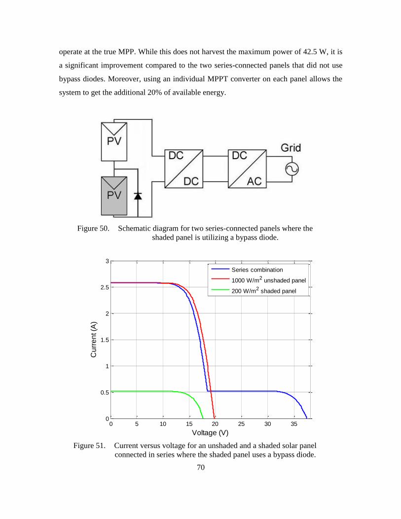
70
operate at the true MPP. While this does not harvest the maximum power of 42.5 W, it is
a significant improvement compared to the two series-connected panels that did not use
bypass diodes. Moreover, using an individual MPPT converter on each panel allows the
system to get the additional 20% of available energy.
Schematic diagram for two series-connected panels where the Figure 50.
shaded panel is utilizing a bypass diode.
Current versus voltage for an unshaded and a shaded solar panel Figure 51.
connected in series where the shaded panel uses a bypass diode.
0 5 10 15 20 25 30 350
0.5
1
1.5
2
2.5
3
Voltage (V)
Cu
rre
nt (A
)
Series combination
1000 W/m2 unshaded panel
200 W/m2 shaded panel
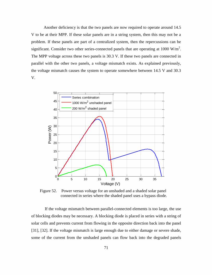
71
Another deficiency is that the two panels are now required to operate around 14.5
V to be at their MPP. If these solar panels are in a string system, then this may not be a
problem. If these panels are part of a centralized system, then the repercussions can be
significant. Consider two other series-connected panels that are operating at 1000 W/m2.
The MPP voltage across these two panels is 30.3 V. If these two panels are connected in
parallel with the other two panels, a voltage mismatch exists. As explained previously,
the voltage mismatch causes the system to operate somewhere between 14.5 V and 30.3
V.
Power versus voltage for an unshaded and a shaded solar panel Figure 52.
connected in series where the shaded panel uses a bypass diode.
If the voltage mismatch between parallel-connected elements is too large, the use
of blocking diodes may be necessary. A blocking diode is placed in series with a string of
solar cells and prevents current from flowing in the opposite direction back into the panel
[31], [32]. If the voltage mismatch is large enough due to either damage or severe shade,
some of the current from the unshaded panels can flow back into the degraded panels
0 5 10 15 20 25 30 350
5
10
15
20
25
30
35
40
45
50
Voltage (V)
Po
we
r (W
)
Series combination
1000 W/m2 unshaded panel
200 W/m2 shaded panel

72
[31]. This is undesirable since the energy flowing back into the degraded panels, which
are consuming power in this scenario, is wasted [31], [32]. While the blocking diode
prevents certain unwanted conditions from occurring, it draws additional power from the
system during normal operation. Employing a boost converter on each panel or with a
string system eliminates the need for blocking diodes.
Finally, certain MPPT algorithms can possibly lock onto the wrong point if there
are multiple local maxima. Typically, there is only one maximum power point; however,
in the presence of mismatched conditions due to shading and bypass diodes, it is possible
to have more than one local maximum as depicted in Figure 52 [4], [25]. In this situation,
the algorithm can possibly oscillate around a local maximum that is not the MPP. Of
note, the centralized and string systems are susceptible to this situation. One possible
solution is to use an algorithm that can find the MPP. With that said, the algorithms used
in this thesis are relatively simple and are not suitable for this task. An alternative
solution is to operate a MPPT converter on each panel as is demonstrated in this thesis.
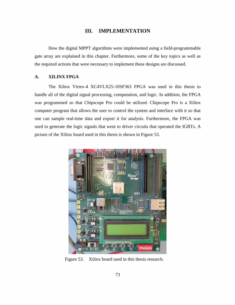
73
III. IMPLEMENTATION
How the digital MPPT algorithms were implemented using a field-programmable
gate array are explained in this chapter. Furthermore, some of the key topics as well as
the required actions that were necessary to implement these designs are discussed.
A. XILINX FPGA
The Xilinx Virtex-4 XC4VLX25-10SF363 FPGA was used in this thesis to
handle all of the digital signal processing, computation, and logic. In addition, the FPGA
was programmed so that Chipscope Pro could be utilized. Chipscope Pro is a Xilinx
computer program that allows the user to control the system and interface with it so that
one can sample real-time data and export it for analysis. Furthermore, the FPGA was
used to generate the logic signals that went to driver circuits that operated the IGBTs. A
picture of the Xilinx board used in this thesis is shown in Figure 53.
Xilinx board used in this thesis research. Figure 53.

74
In order to generate the VHDL code that was loaded into the FPGA, the Xilinx
blockset in Simulink was utilized. A few of the logic designs and algorithms using the
Xilinx blockset in Simulink are contained Appendix B. Once the Xilinx-based design was
complete, the system generator block was utilized to create a Xilinx ISE project file. This
file was then passed to the Xilinx Project Navigator in order to synthesize the VHDL
code used in the FPGA. Finally, Chipscope Pro loaded the VHDL file into the FPGA and
was used to control the system and record data.
B. FIXED-POINT BINARY NUMBERS
Using the Xilinx blockset with this particular FPGA required the use of fixed-
point binary numbers. Binary numbers are chronicled in countless textbooks and papers.
As such, it is not the intent to recount every minuscule detail on the subject. Nevertheless,
a brief explanation of fixed-point binary numbers is essential in order to explain some of
the design considerations that are necessary.
This particular FPGA does not allow for the use of floating point numbers, where
the binary point can be moved in a way similar to how a decimal point is shifted when
using scientific notation. Since the FPGA does not allow this format, fixed-point numbers
were employed. This is where the binary point remains fixed. For each signal, it was
necessary to specify the number of integer bits and the number of fractional bits. In
Figure 54, an example of these options is shown from the output tab on an
adder/subtracter module. Here, one can see that the total number of bits is 23, and the
binary point is placed to the left of the 17th bit; therefore, there are 17 fractional bits in
the output of this module. The other six bits are used to express the integer part as well as
the sign bit. Moreover, it was necessary to specify whether the number was a signed
two’s complement number or an unsigned number. Unsigned numbers mean that the
number can only be expressed as a positive value. Signed two’s complement allowed the
number to be positive or negative. Mostly, signed two’s complement was used in the
algorithm, but counters, which were used to make the MPPT clock signal for example,
employed unsigned numbers.
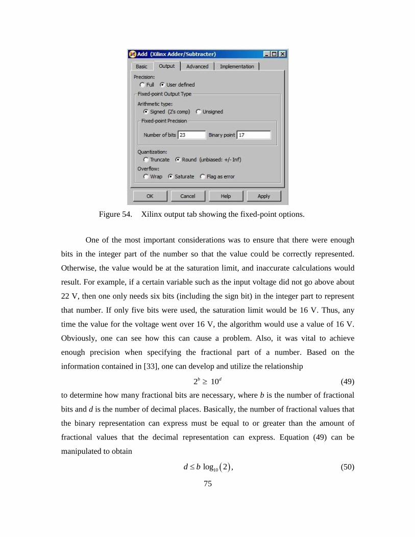
75
Xilinx output tab showing the fixed-point options. Figure 54.
One of the most important considerations was to ensure that there were enough
bits in the integer part of the number so that the value could be correctly represented.
Otherwise, the value would be at the saturation limit, and inaccurate calculations would
result. For example, if a certain variable such as the input voltage did not go above about
22 V, then one only needs six bits (including the sign bit) in the integer part to represent
that number. If only five bits were used, the saturation limit would be 16 V. Thus, any
time the value for the voltage went over 16 V, the algorithm would use a value of 16 V.
Obviously, one can see how this can cause a problem. Also, it was vital to achieve
enough precision when specifying the fractional part of a number. Based on the
information contained in [33], one can develop and utilize the relationship
2 10b d (49)
to determine how many fractional bits are necessary, where b is the number of fractional
bits and d is the number of decimal places. Basically, the number of fractional values that
the binary representation can express must be equal to or greater than the amount of
fractional values that the decimal representation can express. Equation (49) can be
manipulated to obtain
10log 2d b , (50)

76
which is similar to what is described in [33]. Looking back at the example presented by
Figure 54, one sees that there are 17 fractional bits b. From (50), this implies that no more
than five decimal places can be represented accurately; thus, if one wants to represent the
fractional part of a binary number more accurately, then more fractional bits are
necessary.
C. SENSOR CALIBRATION
While testing the system, it was noticed that the values for voltage and current
measured by Chipscope Pro were inaccurate when compared to those taken from a
multimeter. It was deemed necessary to correct for some of the deviations within the
digital algorithm. First, there was a problem with the scaling of the digital signals. After
the analog-to-digital converter (ADC) samples the voltage and current, the conversion
process normalizes them to a value between negative one and one. It is necessary to
multiply this digital value by a corresponding gain in order to get the correct value.
Theoretically, these gains should have been accurate, but they were not and had to be
adjusted by multiplying them by a scaling factor. Also, there was a DC bias in the
average value of the Chipscope measurements. After applying the gain and scaling factor,
the algorithm attempts to add an offset to account for this bias. The gains, offsets, and
scaling factors are documented in Appendix A. While this technique proved fairly useful,
it was not perfect. One can see that some of the measurements were not correct. For
instance, when the system is turned off, the current still reads about 33 mA.
D. DIGITAL FILTERING
The presence of noise made it difficult to run the MPPT algorithms since it was
unable to produce precise measurements for the input voltage and current. This noise was
due to many possible factors. For instance, the quantization process inherently caused
random errors in the value of the measurements. Since the ADC has to, in essence, round
the sampled value to a discrete value, the true value is lost, and error is introduced.
Additionally, the components used to measure these values are not perfect; thus, they
impart some added uncertainty to the measurements. Moreover, the converter introduces
a ripple on the input voltage and current due to the switching taking place. While the

77
ripple is not random, it does produce a deviation from the average value. If one measures
these values in the presence of a substantial ripple, then the measurements can appear to
be grossly different from the average values that are desired. Lastly, small changes in
temperature can cause the voltage and current to fluctuate randomly with noise.
As recorded in laboratory testing, the voltage measurements showed a standard
deviation of about 0.07 V at any constant voltage level. Also, the current measurements
for the boost converter had a standard deviation of approximately 0.05 A at high current
settings around 2.35 A. In addition, the current measurements for the interleaved boost
converter showed a standard deviation of about 0.08 A at high current settings. It makes
sense that the interleaved boost converter has a higher standard deviation. Since the IBC
has an additional transistor, it produces more noise. When the current was fairly low, at
about 0.4 A, the standard deviation was in the vicinity of 0.01 A.
1. First-Order Digital Filter
Consequently, a digital filter was added to the algorithm in order to smooth out
the measured values. The filter took care of two main things. First, it drastically mitigated
the noise that was present in the measurements. Also, it attenuated the ripple that was
present due to the switching action of the converter. For simplicity and ease of
computation, a first-order infinite impulse response (IIR) filter was used. This type of
filter can be described with the difference equation
[ 1] 2 [ ] 1 2 [ ]c s c sy n f T x n f T y n , (51)
where fc is the cutoff frequency and Ts is the sampling period.
In order to understand how this difference equation was developed, the following
derivation is presented in line with [34]. First, consider the transfer function of a low-pass
filter in the Laplace domain such as
2( )
( ) 2
c
c
fY s
X s s f
. (52)
If (52) is converted back into its time-domain equivalent, one gets
( )
2 ( ) 2 ( )c c
dy tf y t f x t
dt . (53)
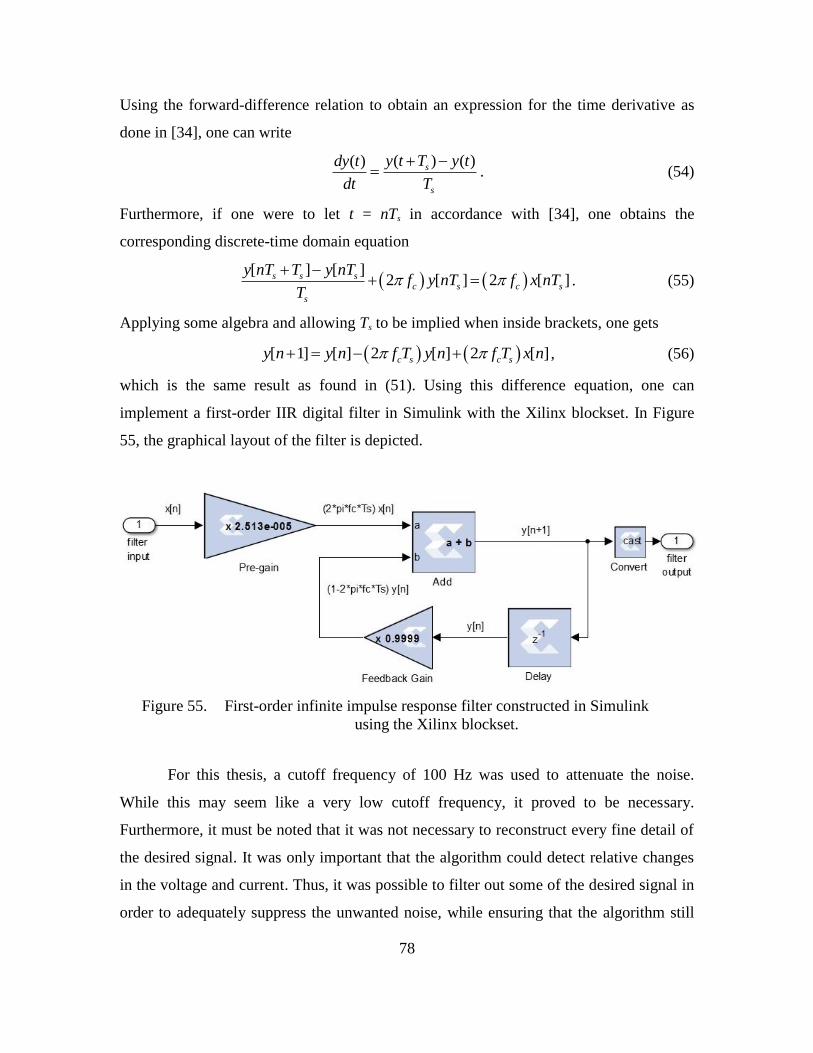
78
Using the forward-difference relation to obtain an expression for the time derivative as
done in [34], one can write
( ) ( )( ) s
s
y t T y tdy t
dt T
. (54)
Furthermore, if one were to let t = nTs in accordance with [34], one obtains the
corresponding discrete-time domain equation
[ ] [ ]
2 [ ] 2 [ ]s s sc s c s
s
y nT T y nTf y nT f x nT
T
. (55)
Applying some algebra and allowing Ts to be implied when inside brackets, one gets
[ 1] [ ] 2 [ ] 2 [ ]c s c sy n y n f T y n f T x n , (56)
which is the same result as found in (51). Using this difference equation, one can
implement a first-order IIR digital filter in Simulink with the Xilinx blockset. In Figure
55, the graphical layout of the filter is depicted.
First-order infinite impulse response filter constructed in Simulink Figure 55.
using the Xilinx blockset.
For this thesis, a cutoff frequency of 100 Hz was used to attenuate the noise.
While this may seem like a very low cutoff frequency, it proved to be necessary.
Furthermore, it must be noted that it was not necessary to reconstruct every fine detail of
the desired signal. It was only important that the algorithm could detect relative changes
in the voltage and current. Thus, it was possible to filter out some of the desired signal in
order to adequately suppress the unwanted noise, while ensuring that the algorithm still

79
worked. In Figure 56, the frequency response for this filter with a cutoff frequency of 100
Hz is displayed in linear magnitude format. In this plot, a few things must be pointed out.
For one, below the cutoff frequency, at least 70% of the original signal’s amplitude
remains. This is important because this is where most of the desired signal lies. At the
switching frequency fsw and higher, the signal’s amplitude is attenuated by a factor of 0.01
or less. This means that the ripple due to switching as well as the noise that is at that
frequency or higher is diminished a great deal. Lastly, this plot shows that the digital low-
pass filter that was designed functions as expected.
2. Results of Filtering
Incorporating this first-order IIR filter was very successful. Additionally, it
allowed the algorithm to run effectively. If the filter was not used, and the noise remained
at its unfiltered levels, this entire research would not have been possible. The frequency
response of the first-order IIR filter in linear magnitude format is displayed in Figure 56.
From this plot, one observes how the higher frequency components are designed to be
attenuated. An example of how this filter suppressed the noise is illustrated in Figure 57.
To create this plot, the measurement noise was incorporated into the Simulink model by
using the random number block. The simulation generates a Gaussian random number
that is scaled appropriately based on the standard deviation in the unfiltered voltage (or
current) measurements. Then it adds that random number to the true value of the
measured parameter. Even though this was a simulation, one can see the difference
between the unfiltered voltage and the filtered voltage. The unfiltered voltage, shown in
blue, has excessive deviations in voltage from the filtered value. As pointed out earlier,
this would potentially confuse the MPPT algorithm and make it virtually impossible to
control the power from the solar panel. In contrast, the filtered voltage, shown in red,
more accurately represents the true value of the actual voltage. Using this signal, one can
adequately control the solar panel with little problems due to noise.
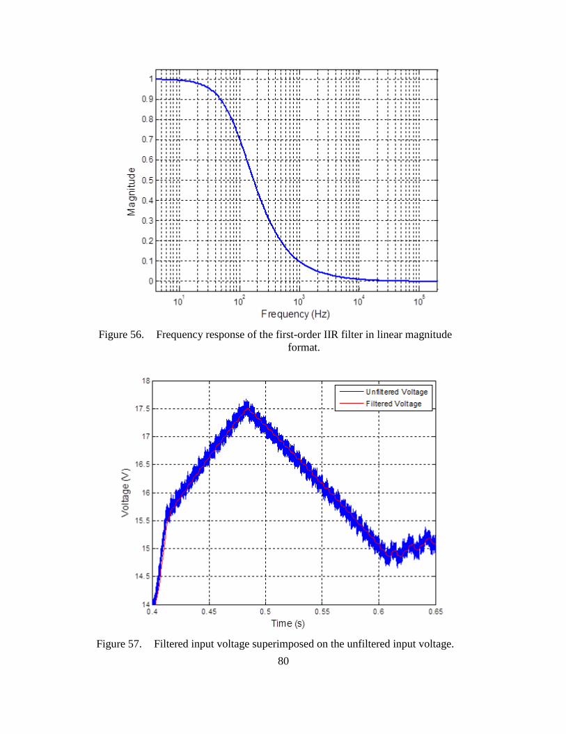
80
Frequency response of the first-order IIR filter in linear magnitude Figure 56.
format.
Filtered input voltage superimposed on the unfiltered input voltage. Figure 57.
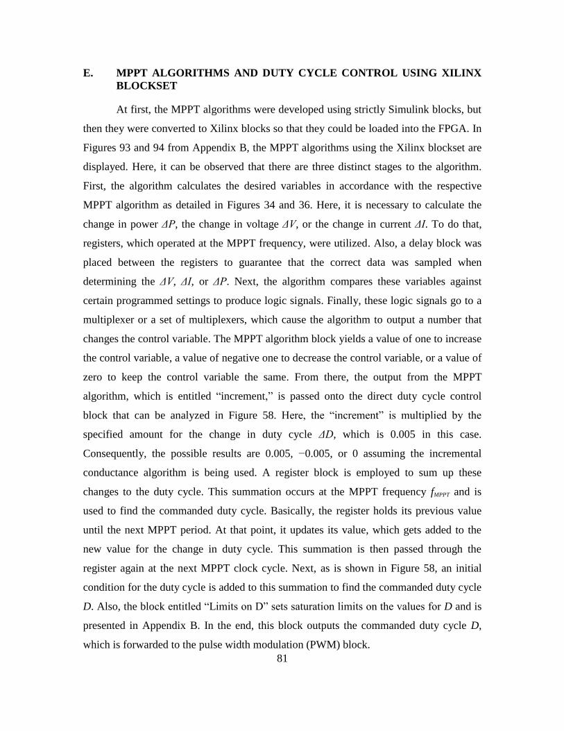
81
E. MPPT ALGORITHMS AND DUTY CYCLE CONTROL USING XILINX
BLOCKSET
At first, the MPPT algorithms were developed using strictly Simulink blocks, but
then they were converted to Xilinx blocks so that they could be loaded into the FPGA. In
Figures 93 and 94 from Appendix B, the MPPT algorithms using the Xilinx blockset are
displayed. Here, it can be observed that there are three distinct stages to the algorithm.
First, the algorithm calculates the desired variables in accordance with the respective
MPPT algorithm as detailed in Figures 34 and 36. Here, it is necessary to calculate the
change in power ΔP, the change in voltage ΔV, or the change in current ΔI. To do that,
registers, which operated at the MPPT frequency, were utilized. Also, a delay block was
placed between the registers to guarantee that the correct data was sampled when
determining the ΔV, ΔI, or ΔP. Next, the algorithm compares these variables against
certain programmed settings to produce logic signals. Finally, these logic signals go to a
multiplexer or a set of multiplexers, which cause the algorithm to output a number that
changes the control variable. The MPPT algorithm block yields a value of one to increase
the control variable, a value of negative one to decrease the control variable, or a value of
zero to keep the control variable the same. From there, the output from the MPPT
algorithm, which is entitled “increment,” is passed onto the direct duty cycle control
block that can be analyzed in Figure 58. Here, the “increment” is multiplied by the
specified amount for the change in duty cycle ΔD, which is 0.005 in this case.
Consequently, the possible results are 0.005, −0.005, or 0 assuming the incremental
conductance algorithm is being used. A register block is employed to sum up these
changes to the duty cycle. This summation occurs at the MPPT frequency fMPPT and is
used to find the commanded duty cycle. Basically, the register holds its previous value
until the next MPPT period. At that point, it updates its value, which gets added to the
new value for the change in duty cycle. This summation is then passed through the
register again at the next MPPT clock cycle. Next, as is shown in Figure 58, an initial
condition for the duty cycle is added to this summation to find the commanded duty cycle
D. Also, the block entitled “Limits on D” sets saturation limits on the values for D and is
presented in Appendix B. In the end, this block outputs the commanded duty cycle D,
which is forwarded to the pulse width modulation (PWM) block.
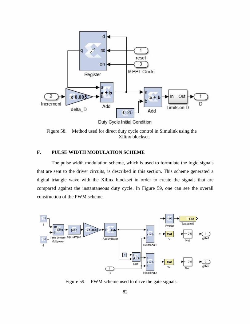
82
Method used for direct duty cycle control in Simulink using the Figure 58.
Xilinx blockset.
F. PULSE WIDTH MODULATION SCHEME
The pulse width modulation scheme, which is used to formulate the logic signals
that are sent to the driver circuits, is described in this section. This scheme generated a
digital triangle wave with the Xilinx blockset in order to create the signals that are
compared against the instantaneous duty cycle. In Figure 59, one can see the overall
construction of the PWM scheme.
PWM scheme used to drive the gate signals. Figure 59.

83
The triangle wave is produced by using a time-division multiplexer that switches
between one and negative one. It does this at a time interval that corresponds to half of
the switching period Tsw. Next, the output from the multiplexer is up-sampled 625 times
within half of Tsw. This makes it so that the samples coming from the multiplexer are at
the clock’s rate of 25 MHz. After that, the signal must be multiplied by 1/625 so that the
accumulator integrates the signal as desired. Over one switching period Tsw, this produces
a triangle wave that starts at zero, ramps up to one, and then ramps down back to zero.
From there, an interleaved triangle wave is made for the realization of the IBC. Here, the
wave must be shifted in time by half of Tsw. To do this, a simple mathematical trick was
employed. The original triangle wave is inverted by multiplying it by negative one. Then,
an amount equal to its amplitude, which is a value of one in this case, is added to this
inverted triangle wave. The resulting signal is a triangle wave with the desired phase
shift. After that, the two triangle waves are compared against the instantaneous duty cycle
to make the appropriate logic signals for each phase.
The logic signals that are sent to the gate drivers on the actual hardware are the
inverse of what is normally used. For instance, when this logic signal is high, the switch
is actually turned off. When this signal is low, the switch is turned on. While this is
counterintuitive, this is how the design of the gate drivers was meant to operate. In the
simulation as well as what is seen on the oscilloscope, this convention was reversed by
the NOT gates, which inverted the logic signals, as is evident in Figure 59.

84
THIS PAGE INTENTIONALLY LEFT BLANK

85
IV. MODELING AND SIMULATION
A. MODELING
The purpose of this chapter is to explain the modeling and simulation used in this
thesis. More specifically, the simulation tools used are described in detail and the results
of those simulations are presented.
1. Modeling the Power Converters using SimPowerSystems in Simulink
SimPowerSystems is a special and powerful library of electrical components and
analysis tools within Simulink that can be assembled to model virtually any electrical
power system [35]. It is a simple and convenient method to simulate a power converter.
One merely has to assemble the correct parts in the appropriate place within the
schematic. In addition to laying out the system correctly, certain settings within each
component must be modified to represent the desired characteristics. In Figure 60, one
sees how the entire system is laid out. Starting from the left, the solar panel is modeled as
a variable current source since the variable that it receives from the solar panel model is a
current. In addition, each component of the IBC is assembled exactly as the schematic
from Figure 21. In the simulation, the inductors are assumed to be lossy while the
capacitors are not. Accordingly, the inductor has an equivalent series resistance (ESR),
and the capacitors do not. Of note, the battery is modeled as a DC voltage source with an
ESR. This allowed the output voltage to resemble the real system to some extent. The
IGBTs and diodes have several settings, which are all detailed in Appendix A. One of
these key features is the fact that both the IGBTs and diodes can be set up to
accommodate losses. In other words, the user can enter an on-state resistance and forward
voltage drop for these components. Finally, the measurement blocks, which have a plus
sign and a minus sign on them, simply enable the simulation to record and report the
value of certain parameters; hence, these blocks are not akin to actual voltage or current
sensors that affect the system. As a final point, the 2nd generation of SimPowerSystems
was used in this thesis.
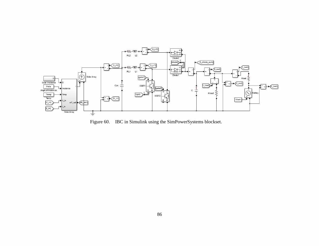
86
IBC in Simulink using the SimPowerSystems blockset. Figure 60.
87
2. Solar Panel Model in Simulink
In this next section, the modeling of the solar panel is explained. Since most of
the theory and equations were presented in Chapter II, this section focuses on how those
equations were constructed in Simulink. In Appendix B, one can examine the way the
solar model equations were implemented using Simulink. This model accepts the solar
irradiance, the temperature, the angle of incidence, the input voltage, and the input
current as inputs. As stated before, this method takes the input voltage and current and
finds the equivalent voltage and current on one cell assuming all other cells are operating
the same. From there, it implements the equations that govern the solar cell. Equations
(3) and (4) can be seen at the top of Figure 91, and in Figure 92, (5) can be identified.
The model is built to accept the two-diode model, so it may seem like there are two
versions of (5) within Figure 92. In this thesis research, only the single-diode model was
used by setting the reference reverse saturation current for diode #2 Is2,ref to zero as seen
in Appendix A. Equation (6) is throughout this entire model in various elements, which
can be recognized in both Figures 91 and 92. After executing the equations, the current
through the entire array is calculated as described in Chapter II near (7). Additionally,
this model finds the solar cell efficiency, which is the amount of power the panel puts out
divided by the amount of power incident upon its surface. This calculation can be seen in
the lower right portion of Figure 92. Finally, it outputs the updated input current as well
as the solar cell efficiency.
B. SIMULATION
In this section, the specific details of the simulation profile and parameters are
described. The results of these tests are presented and explained thoroughly. For instance,
the speed of each algorithm’s power response is analyzed, and how each algorithm
tracked the MPP is shown. Furthermore, differences in the two algorithms are pointed
out. Of note, these simulation results only concentrate on the interleaved boost converter
because it is one of the main emphases of this thesis.
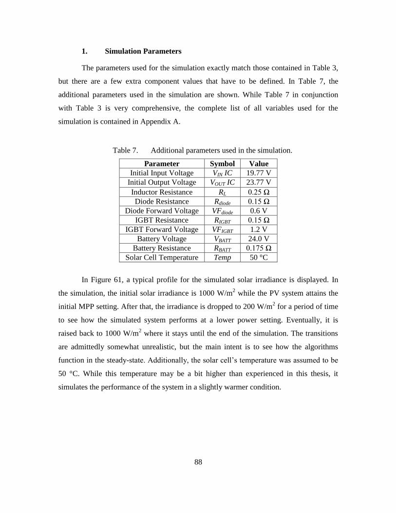
88
1. Simulation Parameters
The parameters used for the simulation exactly match those contained in Table 3,
but there are a few extra component values that have to be defined. In Table 7, the
additional parameters used in the simulation are shown. While Table 7 in conjunction
with Table 3 is very comprehensive, the complete list of all variables used for the
simulation is contained in Appendix A.
Table 7. Additional parameters used in the simulation.
Parameter Symbol Value
Initial Input Voltage VIN IC
19.77 V
Initial Output Voltage VOUT IC 23.77 V
Inductor Resistance RL 0.25 Ω
Diode Resistance Rdiode 0.15 Ω
Diode Forward Voltage VFdiode 0.6 V
IGBT Resistance RIGBT 0.15 Ω
IGBT Forward Voltage VFIGBT 1.2 V
Battery Voltage VBATT 24.0 V
Battery Resistance RBATT 0.175 Ω
Solar Cell Temperature Temp 50 °C
In Figure 61, a typical profile for the simulated solar irradiance is displayed. In
the simulation, the initial solar irradiance is 1000 W/m2 while the PV system attains the
initial MPP setting. After that, the irradiance is dropped to 200 W/m2 for a period of time
to see how the simulated system performs at a lower power setting. Eventually, it is
raised back to 1000 W/m2 where it stays until the end of the simulation. The transitions
are admittedly somewhat unrealistic, but the main intent is to see how the algorithms
function in the steady-state. Additionally, the solar cell’s temperature was assumed to be
50 °C. While this temperature may be a bit higher than experienced in this thesis, it
simulates the performance of the system in a slightly warmer condition.
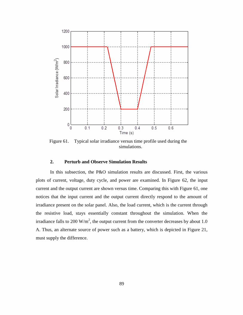
89
Typical solar irradiance versus time profile used during the Figure 61.
simulations.
2. Perturb and Observe Simulation Results
In this subsection, the P&O simulation results are discussed. First, the various
plots of current, voltage, duty cycle, and power are examined. In Figure 62, the input
current and the output current are shown versus time. Comparing this with Figure 61, one
notices that the input current and the output current directly respond to the amount of
irradiance present on the solar panel. Also, the load current, which is the current through
the resistive load, stays essentially constant throughout the simulation. When the
irradiance falls to 200 W/m2, the output current from the converter decreases by about 1.0
A. Thus, an alternate source of power such as a battery, which is depicted in Figure 21,
must supply the difference.
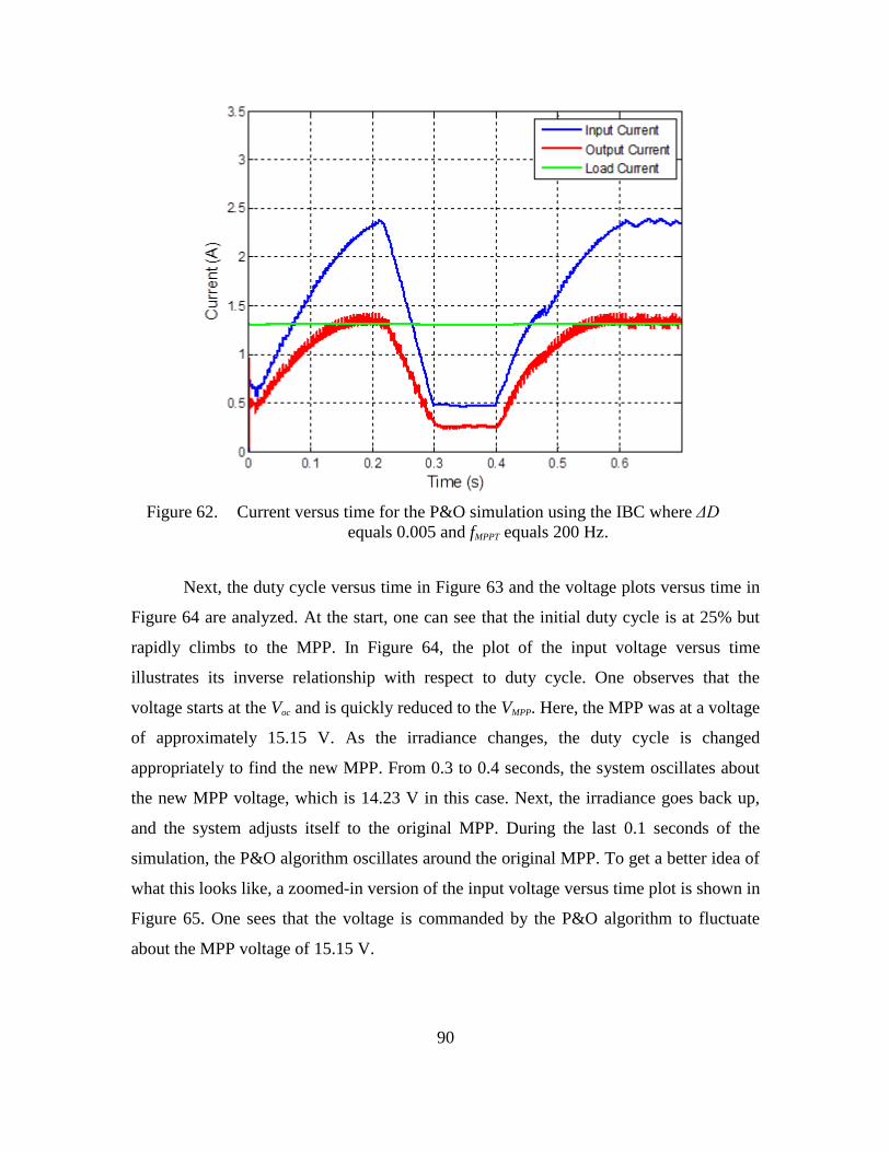
90
Current versus time for the P&O simulation using the IBC where ΔD Figure 62.
equals 0.005 and fMPPT equals 200 Hz.
Next, the duty cycle versus time in Figure 63 and the voltage plots versus time in
Figure 64 are analyzed. At the start, one can see that the initial duty cycle is at 25% but
rapidly climbs to the MPP. In Figure 64, the plot of the input voltage versus time
illustrates its inverse relationship with respect to duty cycle. One observes that the
voltage starts at the Voc and is quickly reduced to the VMPP. Here, the MPP was at a voltage
of approximately 15.15 V. As the irradiance changes, the duty cycle is changed
appropriately to find the new MPP. From 0.3 to 0.4 seconds, the system oscillates about
the new MPP voltage, which is 14.23 V in this case. Next, the irradiance goes back up,
and the system adjusts itself to the original MPP. During the last 0.1 seconds of the
simulation, the P&O algorithm oscillates around the original MPP. To get a better idea of
what this looks like, a zoomed-in version of the input voltage versus time plot is shown in
Figure 65. One sees that the voltage is commanded by the P&O algorithm to fluctuate
about the MPP voltage of 15.15 V.
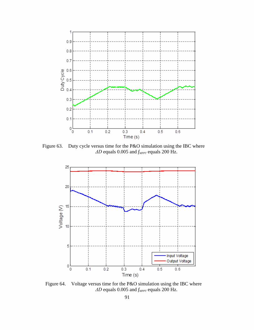
91
Duty cycle versus time for the P&O simulation using the IBC where Figure 63.
ΔD equals 0.005 and fMPPT equals 200 Hz.
Voltage versus time for the P&O simulation using the IBC where Figure 64.
ΔD equals 0.005 and fMPPT equals 200 Hz.
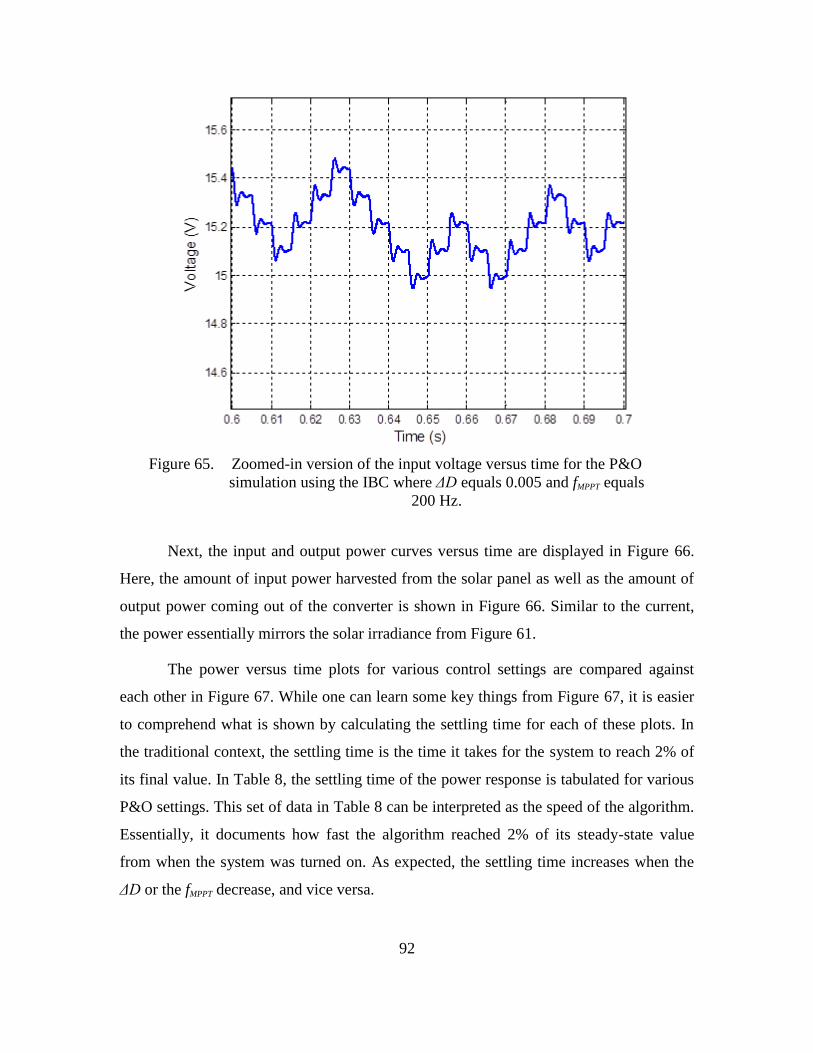
92
Zoomed-in version of the input voltage versus time for the P&O Figure 65.
simulation using the IBC where ΔD equals 0.005 and fMPPT equals
200 Hz.
Next, the input and output power curves versus time are displayed in Figure 66.
Here, the amount of input power harvested from the solar panel as well as the amount of
output power coming out of the converter is shown in Figure 66. Similar to the current,
the power essentially mirrors the solar irradiance from Figure 61.
The power versus time plots for various control settings are compared against
each other in Figure 67. While one can learn some key things from Figure 67, it is easier
to comprehend what is shown by calculating the settling time for each of these plots. In
the traditional context, the settling time is the time it takes for the system to reach 2% of
its final value. In Table 8, the settling time of the power response is tabulated for various
P&O settings. This set of data in Table 8 can be interpreted as the speed of the algorithm.
Essentially, it documents how fast the algorithm reached 2% of its steady-state value
from when the system was turned on. As expected, the settling time increases when the
ΔD or the fMPPT decrease, and vice versa.
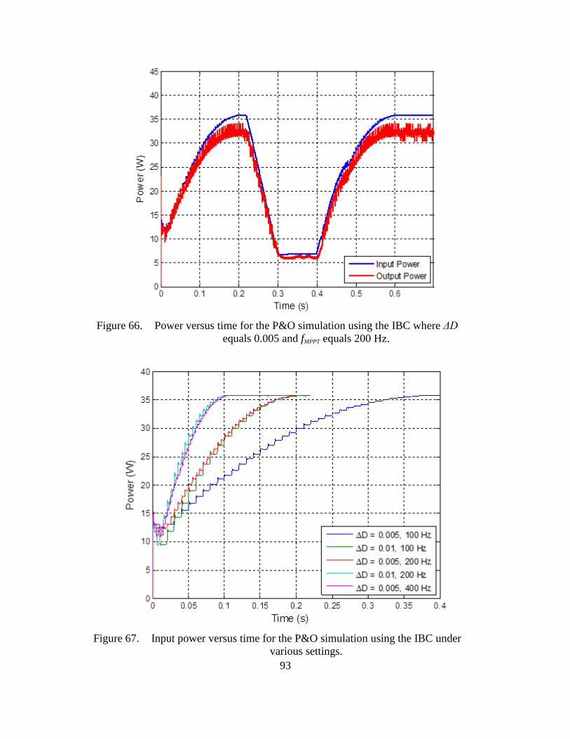
93
Power versus time for the P&O simulation using the IBC where ΔD Figure 66.
equals 0.005 and fMPPT equals 200 Hz.
Input power versus time for the P&O simulation using the IBC under Figure 67.
various settings.
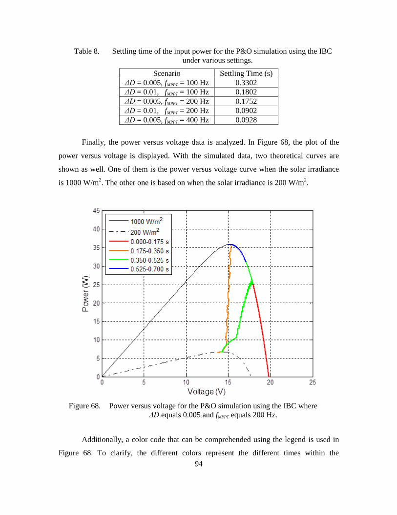
94
Table 8. Settling time of the input power for the P&O simulation using the IBC
under various settings.
Scenario Settling Time (s)
ΔD = 0.005, fMPPT = 100 Hz 0.3302
ΔD = 0.01, fMPPT = 100 Hz 0.1802
ΔD = 0.005, fMPPT = 200 Hz 0.1752
ΔD = 0.01, fMPPT = 200 Hz 0.0902
ΔD = 0.005, fMPPT = 400 Hz 0.0928
Finally, the power versus voltage data is analyzed. In Figure 68, the plot of the
power versus voltage is displayed. With the simulated data, two theoretical curves are
shown as well. One of them is the power versus voltage curve when the solar irradiance
is 1000 W/m2. The other one is based on when the solar irradiance is 200 W/m
2.
Power versus voltage for the P&O simulation using the IBC where Figure 68.
ΔD equals 0.005 and fMPPT equals 200 Hz.
Additionally, a color code that can be comprehended using the legend is used in
Figure 68. To clarify, the different colors represent the different times within the
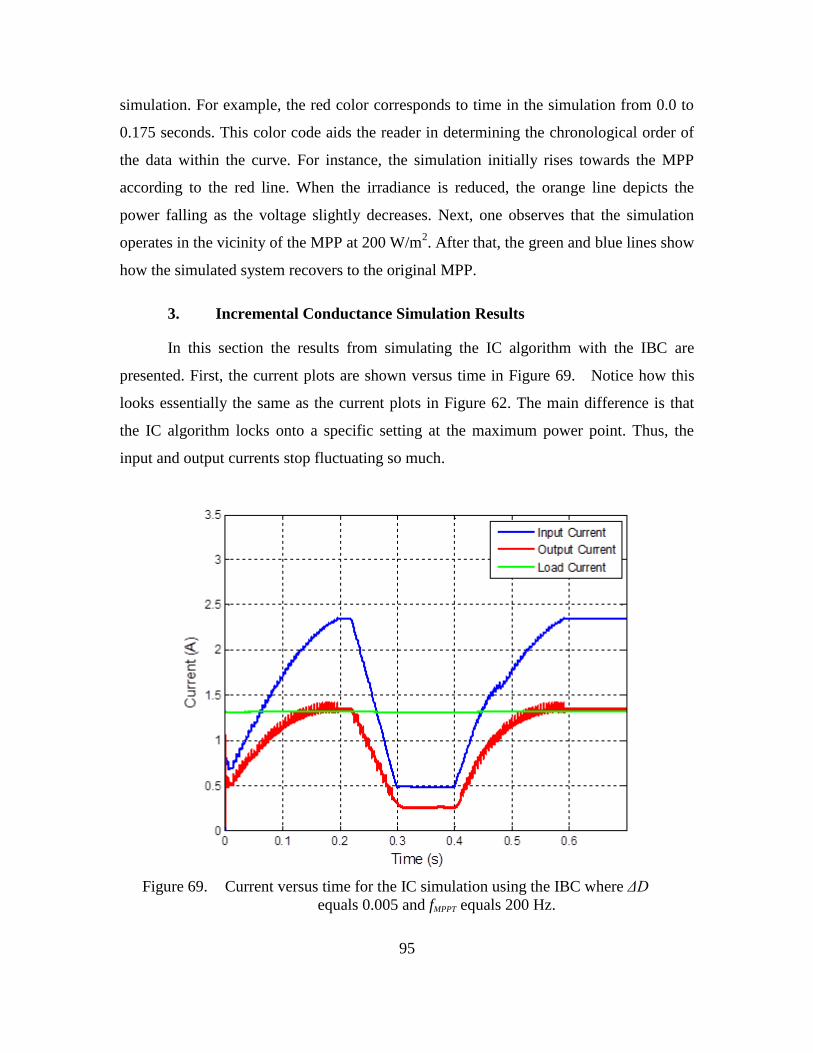
95
simulation. For example, the red color corresponds to time in the simulation from 0.0 to
0.175 seconds. This color code aids the reader in determining the chronological order of
the data within the curve. For instance, the simulation initially rises towards the MPP
according to the red line. When the irradiance is reduced, the orange line depicts the
power falling as the voltage slightly decreases. Next, one observes that the simulation
operates in the vicinity of the MPP at 200 W/m2. After that, the green and blue lines show
how the simulated system recovers to the original MPP.
3. Incremental Conductance Simulation Results
In this section the results from simulating the IC algorithm with the IBC are
presented. First, the current plots are shown versus time in Figure 69. Notice how this
looks essentially the same as the current plots in Figure 62. The main difference is that
the IC algorithm locks onto a specific setting at the maximum power point. Thus, the
input and output currents stop fluctuating so much.
Current versus time for the IC simulation using the IBC where ΔD Figure 69.
equals 0.005 and fMPPT equals 200 Hz.
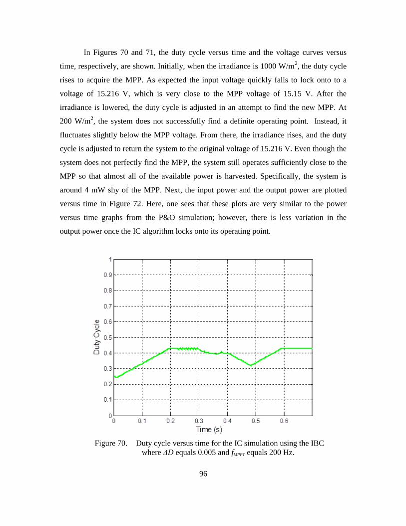
96
In Figures 70 and 71, the duty cycle versus time and the voltage curves versus
time, respectively, are shown. Initially, when the irradiance is 1000 W/m2, the duty cycle
rises to acquire the MPP. As expected the input voltage quickly falls to lock onto to a
voltage of 15.216 V, which is very close to the MPP voltage of 15.15 V. After the
irradiance is lowered, the duty cycle is adjusted in an attempt to find the new MPP. At
200 W/m2, the system does not successfully find a definite operating point. Instead, it
fluctuates slightly below the MPP voltage. From there, the irradiance rises, and the duty
cycle is adjusted to return the system to the original voltage of 15.216 V. Even though the
system does not perfectly find the MPP, the system still operates sufficiently close to the
MPP so that almost all of the available power is harvested. Specifically, the system is
around 4 mW shy of the MPP. Next, the input power and the output power are plotted
versus time in Figure 72. Here, one sees that these plots are very similar to the power
versus time graphs from the P&O simulation; however, there is less variation in the
output power once the IC algorithm locks onto its operating point.
Duty cycle versus time for the IC simulation using the IBC Figure 70.
where ΔD equals 0.005 and fMPPT equals 200 Hz.
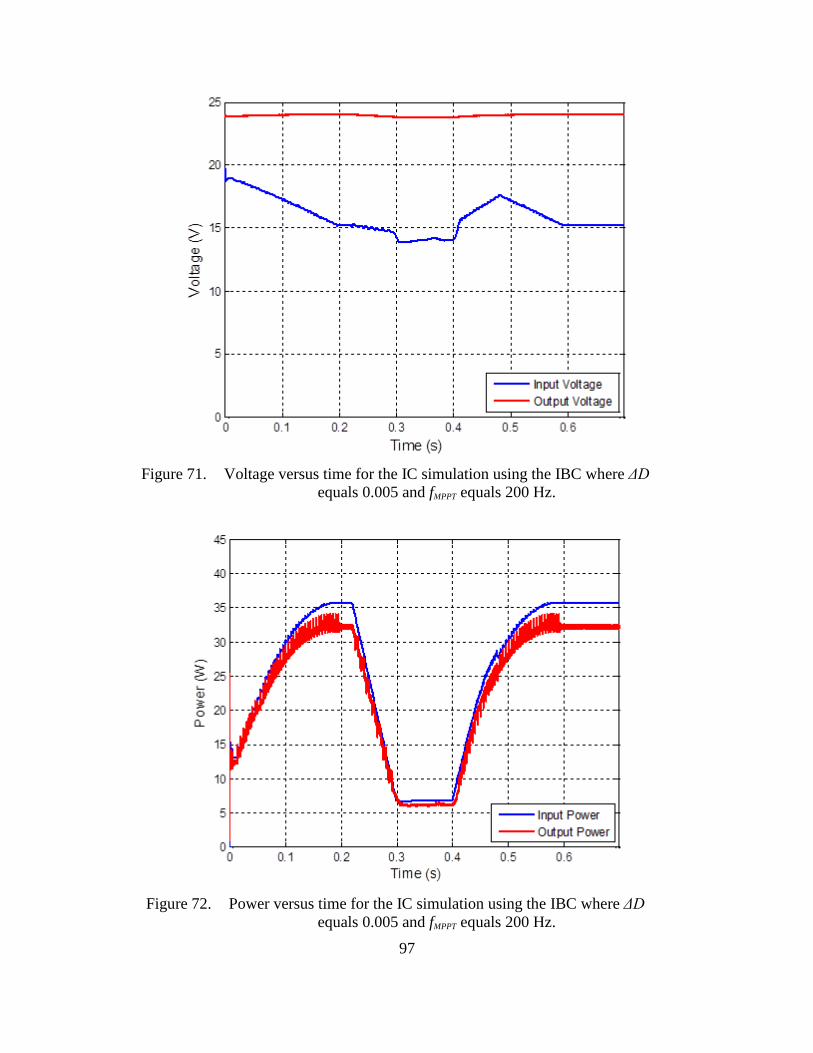
97
Voltage versus time for the IC simulation using the IBC where ΔD Figure 71.
equals 0.005 and fMPPT equals 200 Hz.
Power versus time for the IC simulation using the IBC where ΔD Figure 72.
equals 0.005 and fMPPT equals 200 Hz.
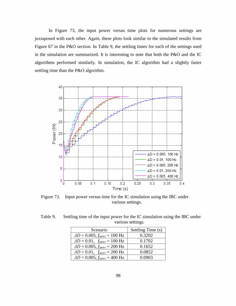
98
In Figure 73, the input power versus time plots for numerous settings are
juxtaposed with each other. Again, these plots look similar to the simulated results from
Figure 67 in the P&O section. In Table 9, the settling times for each of the settings used
in the simulation are summarized. It is interesting to note that both the P&O and the IC
algorithms performed similarly. In simulation, the IC algorithm had a slightly faster
settling time than the P&O algorithm.
Input power versus time for the IC simulation using the IBC under Figure 73.
various settings.
Table 9. Settling time of the input power for the IC simulation using the IBC under
various settings.
Scenario Settling Time (s)
ΔD = 0.005, fMPPT = 100 Hz 0.3202
ΔD = 0.01, fMPPT = 100 Hz 0.1702
ΔD = 0.005, fMPPT = 200 Hz 0.1652
ΔD = 0.01, fMPPT = 200 Hz 0.0852
ΔD = 0.005, fMPPT = 400 Hz 0.0903
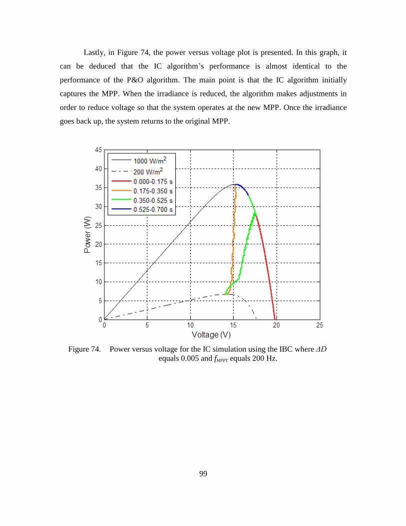
99
Lastly, in Figure 74, the power versus voltage plot is presented. In this graph, it
can be deduced that the IC algorithm’s performance is almost identical to the
performance of the P&O algorithm. The main point is that the IC algorithm initially
captures the MPP. When the irradiance is reduced, the algorithm makes adjustments in
order to reduce voltage so that the system operates at the new MPP. Once the irradiance
goes back up, the system returns to the original MPP.
Power versus voltage for the IC simulation using the IBC where ΔD Figure 74.
equals 0.005 and fMPPT equals 200 Hz.

100
THIS PAGE INTENTIONALLY LEFT BLANK

101
V. EXPERIMENTAL TESTING
The purpose of this chapter is to describe the experimental testing that was
conducted in this thesis. More precisely, the experimental setup is explained, and the
results of those experiments are displayed.
A. EXPERIMENTAL SETUP
In order to understand how the experimental testing was conducted, one must first
reference Figure 21. The main components of the PV system were connected as depicted
in this schematic diagram of the interleaved boost converter except that a DC voltage
source was used primarily instead of a battery. This was done to simulate a battery that
had a consistent 24 V output voltage. It must be noted that the system was briefly hooked
up to an actual battery in order to prove that it worked. During this short test, the system
operated just the same as using the DC voltage source.
In Figure 75, a picture of the test setup is displayed. Here, one can see the overall
layout of the different components and their physical relationship to one another. In this
picture, one can see four multimeters, which were used to measure the voltage and
current for the input and the output. Also, there is an oscilloscope that displayed various
waveforms such as the inductor currents, the input voltage, the output voltage, the input
current, the output current, and the gate signal for one of the transistors. Additionally, one
can see that the solar panel was placed outside, and the wires were fed through the
window. In Figure 76, one can see how the solar panel was set up on the ground with its
wires hanging outside the window. Also, the resistive load is depicted in Figure 77. As
one may ascertain, the resistive load is simply a number of resistors in parallel. In Figure
78, the FPGA boards, which were assembled above the power converter board, were
temporarily separated from the IBC to expose the components of the power converter.
One notices that this board is more than just the basic components of the power converter
as depicted in Figure 21. There are several other components that are needed to make the
IBC work, such as the gate driver circuits, voltage regulators, measurement devices, and
a heat sink with a fan.
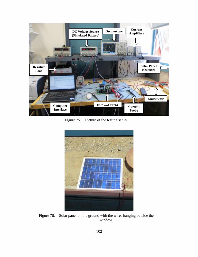
102
Picture of the testing setup. Figure 75.
Solar panel on the ground with the wires hanging outside the Figure 76.
window.
Oscilloscope DC Voltage Source
(Simulated Battery)
IBC and FPGA
Solar Panel
(Outside)
Computer
Interface
Resistive
Load
Multimeter
Current
Probe
Current
Amplifiers
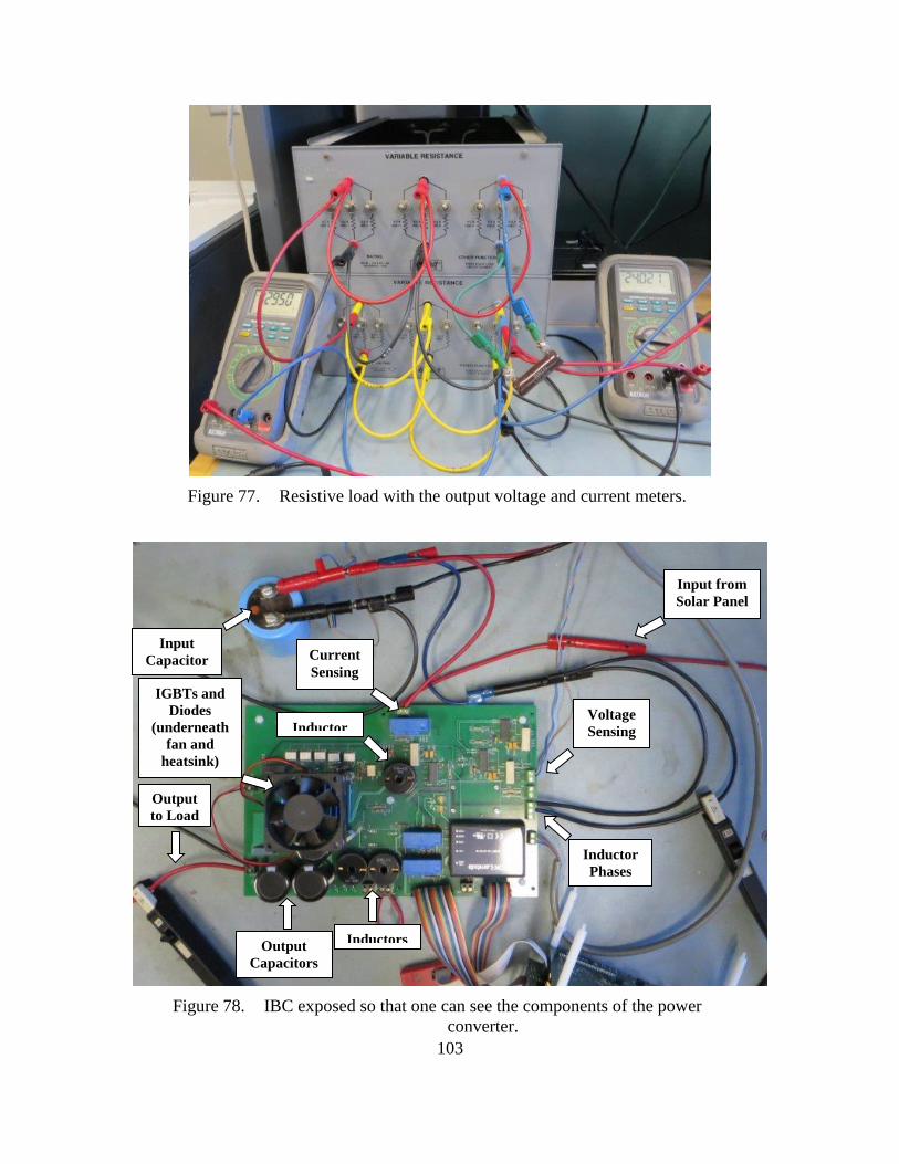
103
Resistive load with the output voltage and current meters. Figure 77.
IBC exposed so that one can see the components of the power Figure 78.
converter.
Input
Capacitor
Output
Capacitors
Inductors
Current
Sensing
Inductor
Phases
IGBTs and
Diodes
(underneath
fan and
heatsink)
Voltage
Sensing
Input from
Solar Panel
Output
to Load
Inductor
=

104
All of these miscellaneous parts were necessary to operate the converter, and that
is what is seen in Figure 78. Lastly, one can discern the electrical connections that were
made if one follows the wires. For example, one sees that the input from the solar panel is
fed through a current sensing device and then goes to the input capacitor. From there, the
wires split so that two separate phases connect with their respective inductors. In the
vicinity of the output capacitors, a set of wires exists in order to feed the output current
into the load and the simulated battery.
B. TESTING
In this section, the testing of the PV system is explained, and the parameters used
in the actual tests are described in detail. Similar to Chapter IV, certain results were
analyzed, such as the speed of the algorithm under different control parameters and the
ability of the system to track the MPP. It must be noted that mostly results from testing
the interleaved boost converter are presented since the main focus of this thesis has been
on the IBC. Nevertheless, at the end of this section, a comparison is made between the
boost converter and the IBC with respect to ripple and efficiency.
1. Testing Parameters
In this next section, the parameters utilized in the experimental testing are
discussed. As for the components used in the testing of the PV system, they were the
same as the theoretical values used in the simulation, and the numbers previously
presented in Table 3 may be referenced once again for the experimental testing. There
were several tests that were performed in order to see how the actual system responded.
For instance, one of these tests involved turning the converter off and then back on to see
how long it took for the system to reach full power. Additionally, the steady-state
operation was analyzed. By recording voltages and currents at the input and the output
while in the steady-state, the converter efficiency was verified. Another experiment
involved looking at the waveforms for the inductor currents and output voltage in order to
ascertain the ripple in each. Moreover, the operation of the system was investigated while
the solar panel was experiencing a shading event. A shading event was created by
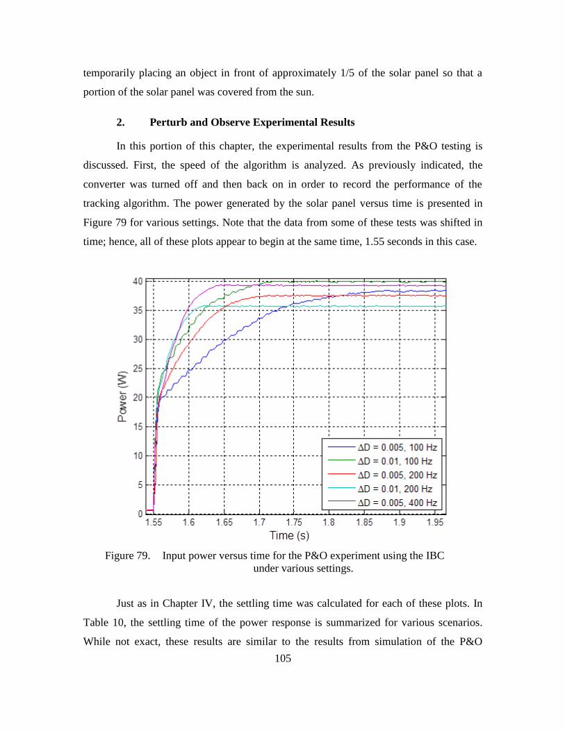
105
temporarily placing an object in front of approximately 1/5 of the solar panel so that a
portion of the solar panel was covered from the sun.
2. Perturb and Observe Experimental Results
In this portion of this chapter, the experimental results from the P&O testing is
discussed. First, the speed of the algorithm is analyzed. As previously indicated, the
converter was turned off and then back on in order to record the performance of the
tracking algorithm. The power generated by the solar panel versus time is presented in
Figure 79 for various settings. Note that the data from some of these tests was shifted in
time; hence, all of these plots appear to begin at the same time, 1.55 seconds in this case.
Input power versus time for the P&O experiment using the IBC Figure 79.
under various settings.
Just as in Chapter IV, the settling time was calculated for each of these plots. In
Table 10, the settling time of the power response is summarized for various scenarios.
While not exact, these results are similar to the results from simulation of the P&O
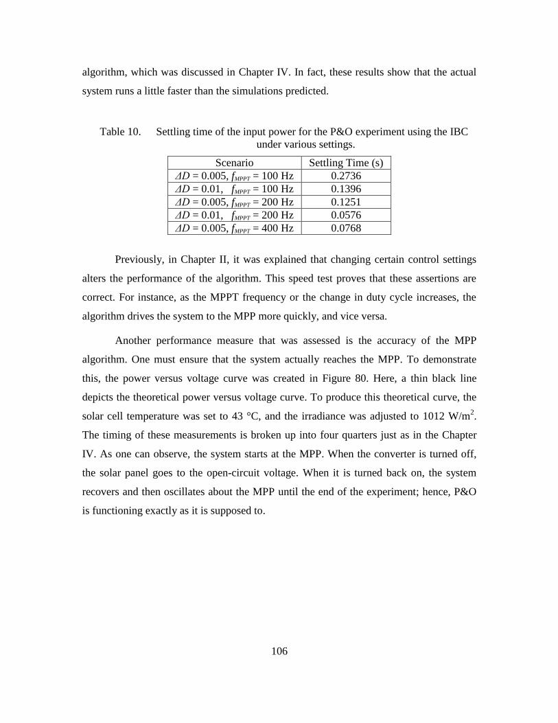
106
algorithm, which was discussed in Chapter IV. In fact, these results show that the actual
system runs a little faster than the simulations predicted.
Table 10. Settling time of the input power for the P&O experiment using the IBC
under various settings.
Scenario Settling Time (s)
ΔD = 0.005, fMPPT = 100 Hz 0.2736
ΔD = 0.01, fMPPT = 100 Hz 0.1396
ΔD = 0.005, fMPPT = 200 Hz 0.1251
ΔD = 0.01, fMPPT = 200 Hz 0.0576
ΔD = 0.005, fMPPT = 400 Hz 0.0768
Previously, in Chapter II, it was explained that changing certain control settings
alters the performance of the algorithm. This speed test proves that these assertions are
correct. For instance, as the MPPT frequency or the change in duty cycle increases, the
algorithm drives the system to the MPP more quickly, and vice versa.
Another performance measure that was assessed is the accuracy of the MPP
algorithm. One must ensure that the system actually reaches the MPP. To demonstrate
this, the power versus voltage curve was created in Figure 80. Here, a thin black line
depicts the theoretical power versus voltage curve. To produce this theoretical curve, the
solar cell temperature was set to 43 °C, and the irradiance was adjusted to 1012 W/m2.
The timing of these measurements is broken up into four quarters just as in the Chapter
IV. As one can observe, the system starts at the MPP. When the converter is turned off,
the solar panel goes to the open-circuit voltage. When it is turned back on, the system
recovers and then oscillates about the MPP until the end of the experiment; hence, P&O
is functioning exactly as it is supposed to.
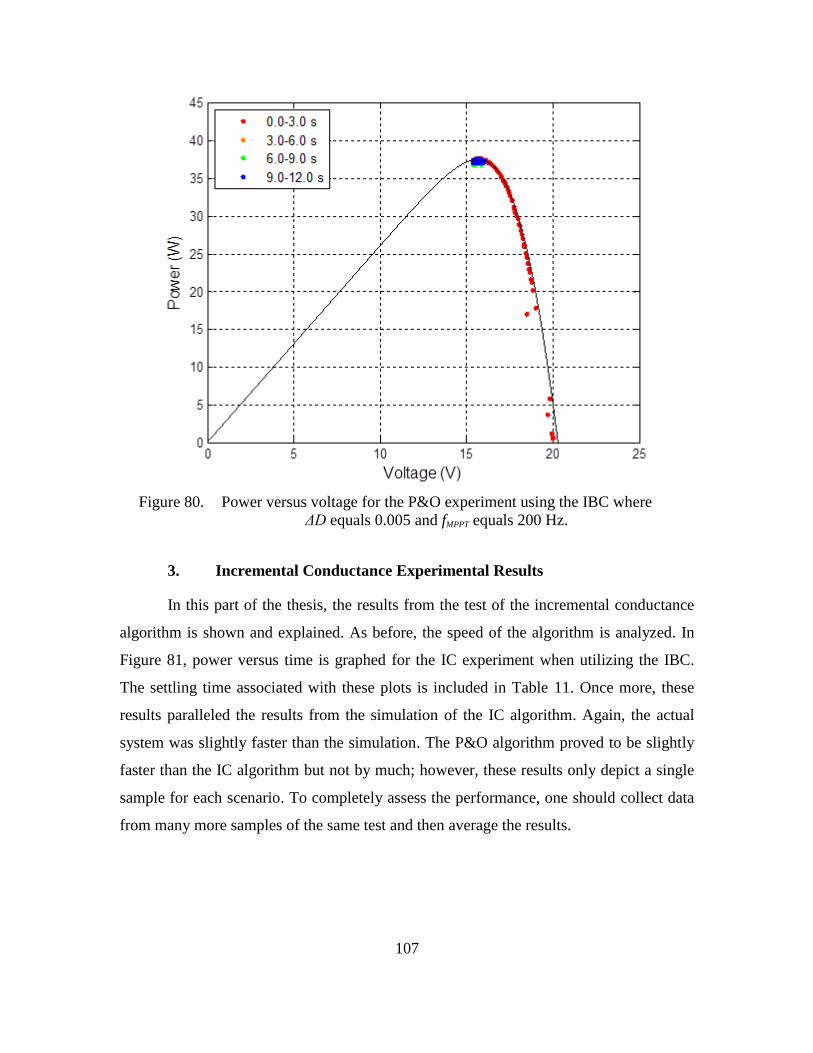
107
Power versus voltage for the P&O experiment using the IBC where Figure 80.
ΔD equals 0.005 and fMPPT equals 200 Hz.
3. Incremental Conductance Experimental Results
In this part of the thesis, the results from the test of the incremental conductance
algorithm is shown and explained. As before, the speed of the algorithm is analyzed. In
Figure 81, power versus time is graphed for the IC experiment when utilizing the IBC.
The settling time associated with these plots is included in Table 11. Once more, these
results paralleled the results from the simulation of the IC algorithm. Again, the actual
system was slightly faster than the simulation. The P&O algorithm proved to be slightly
faster than the IC algorithm but not by much; however, these results only depict a single
sample for each scenario. To completely assess the performance, one should collect data
from many more samples of the same test and then average the results.
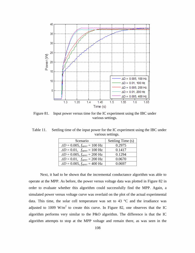
108
Input power versus time for the IC experiment using the IBC under Figure 81.
various settings.
Table 11. Settling time of the input power for the IC experiment using the IBC under
various settings.
Scenario Settling Time (s)
ΔD = 0.005, fMPPT = 100 Hz 0.2975
ΔD = 0.01, fMPPT = 100 Hz 0.1417
ΔD = 0.005, fMPPT = 200 Hz 0.1294
ΔD = 0.01, fMPPT = 200 Hz 0.0670
ΔD = 0.005, fMPPT = 400 Hz 0.0697
Next, it had to be shown that the incremental conductance algorithm was able to
operate at the MPP. As before, the power versus voltage data was plotted in Figure 82 in
order to evaluate whether this algorithm could successfully find the MPP. Again, a
simulated power versus voltage curve was overlaid on the plot of the actual experimental
data. This time, the solar cell temperature was set to 43 °C and the irradiance was
adjusted to 1009 W/m2 to create this curve. In Figure 82, one observes that the IC
algorithm performs very similar to the P&O algorithm. The difference is that the IC
algorithm attempts to stop at the MPP voltage and remain there, as was seen in the
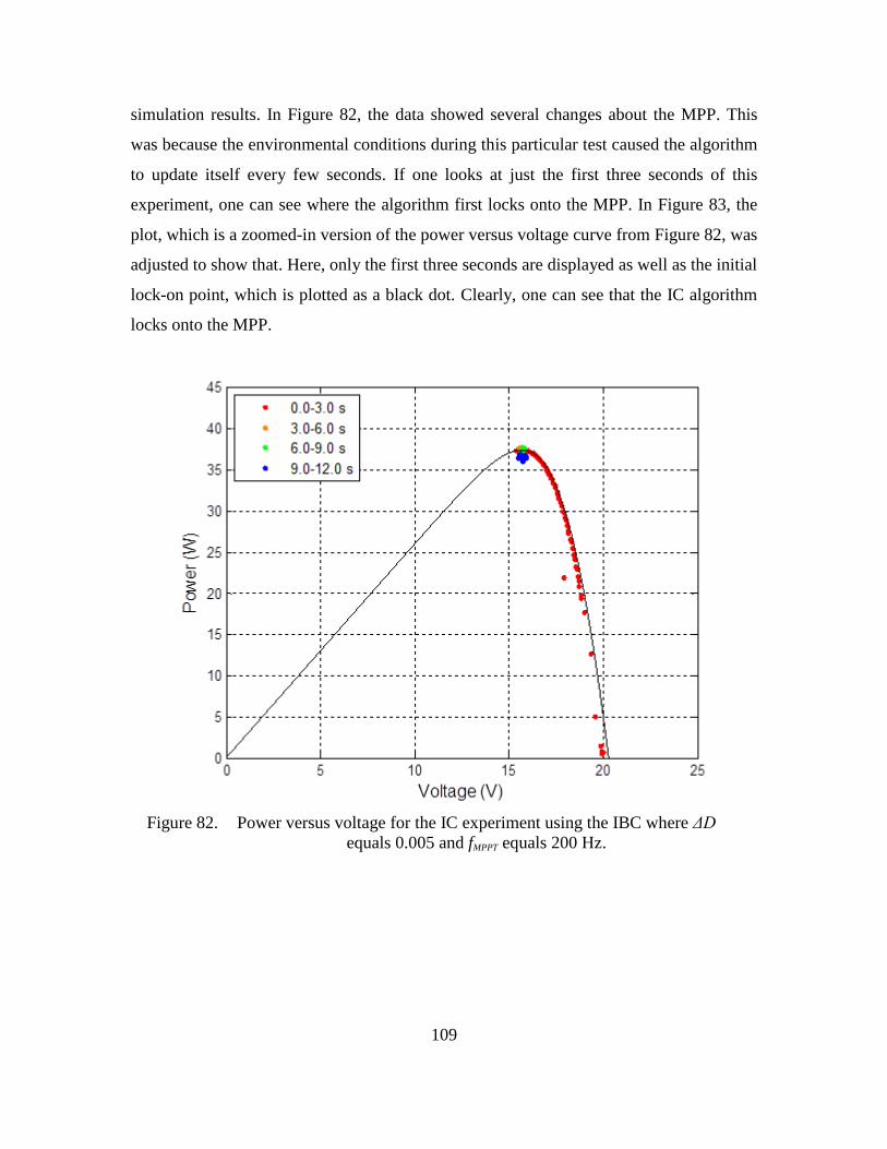
109
simulation results. In Figure 82, the data showed several changes about the MPP. This
was because the environmental conditions during this particular test caused the algorithm
to update itself every few seconds. If one looks at just the first three seconds of this
experiment, one can see where the algorithm first locks onto the MPP. In Figure 83, the
plot, which is a zoomed-in version of the power versus voltage curve from Figure 82, was
adjusted to show that. Here, only the first three seconds are displayed as well as the initial
lock-on point, which is plotted as a black dot. Clearly, one can see that the IC algorithm
locks onto the MPP.
Power versus voltage for the IC experiment using the IBC where ΔD Figure 82.
equals 0.005 and fMPPT equals 200 Hz.
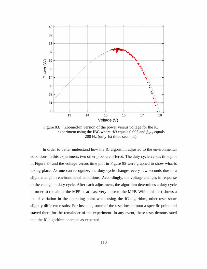
110
Zoomed-in version of the power versus voltage for the IC Figure 83.
experiment using the IBC where ΔD equals 0.005 and fMPPT equals
200 Hz (only 1st three seconds).
In order to better understand how the IC algorithm adjusted to the environmental
conditions in this experiment, two other plots are offered. The duty cycle versus time plot
in Figure 84 and the voltage versus time plot in Figure 85 were graphed to show what is
taking place. As one can recognize, the duty cycle changes every few seconds due to a
slight change in environmental conditions. Accordingly, the voltage changes in response
to the change in duty cycle. After each adjustment, the algorithm determines a duty cycle
in order to remain at the MPP or at least very close to the MPP. While this test shows a
lot of variation in the operating point when using the IC algorithm, other tests show
slightly different results. For instance, some of the tests locked onto a specific point and
stayed there for the remainder of the experiment. In any event, these tests demonstrated
that the IC algorithm operated as expected.
13 14 15 16 17 18
30
31
32
33
34
35
36
37
38
39
40
Voltage (V)
Po
we
r (W
)
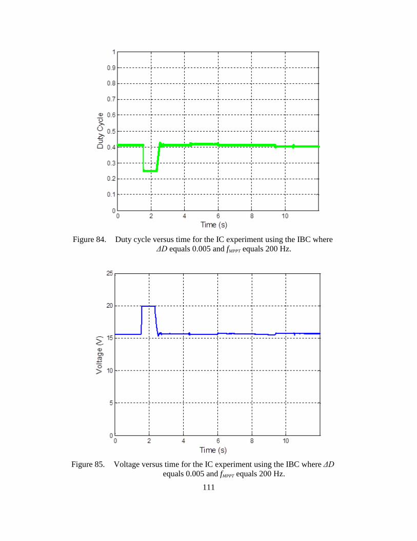
111
Duty cycle versus time for the IC experiment using the IBC where Figure 84.
ΔD equals 0.005 and fMPPT equals 200 Hz.
Voltage versus time for the IC experiment using the IBC where ΔD Figure 85.
equals 0.005 and fMPPT equals 200 Hz.
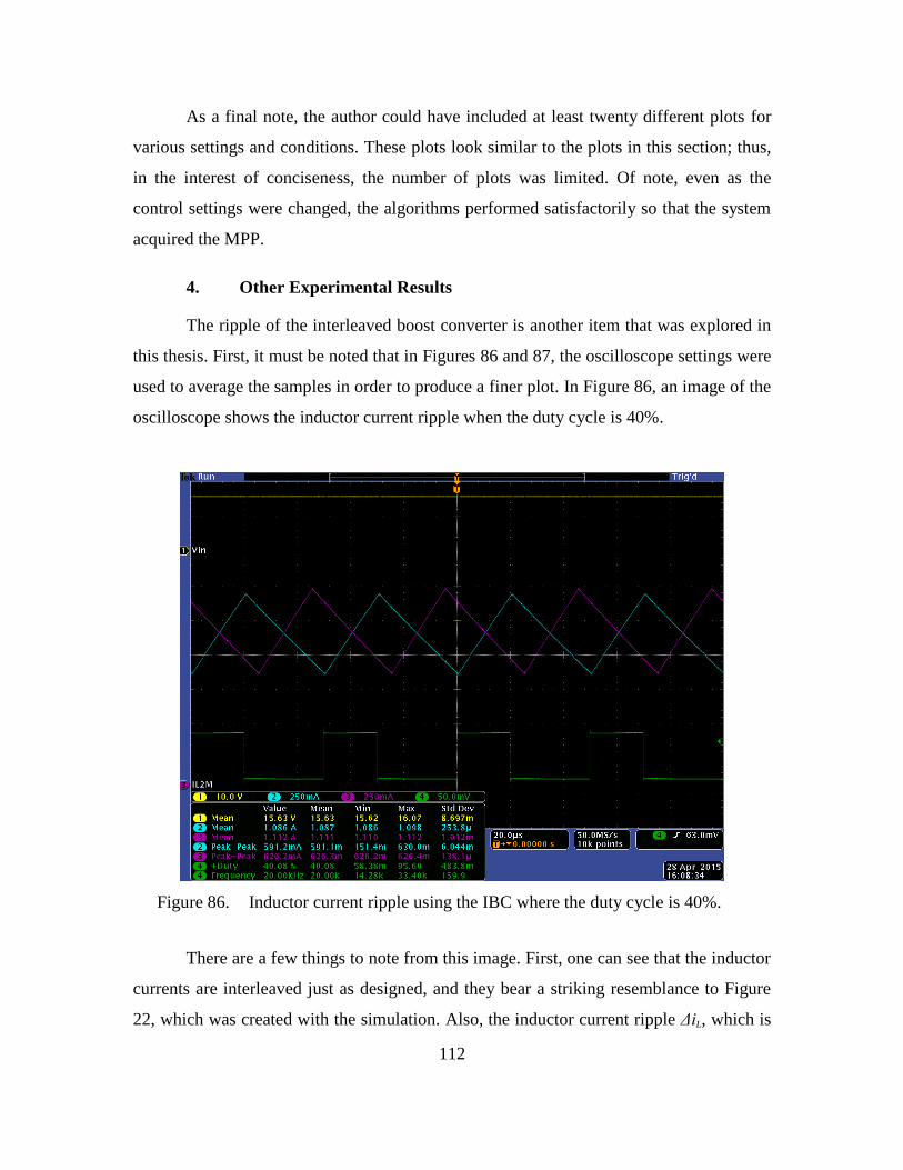
112
As a final note, the author could have included at least twenty different plots for
various settings and conditions. These plots look similar to the plots in this section; thus,
in the interest of conciseness, the number of plots was limited. Of note, even as the
control settings were changed, the algorithms performed satisfactorily so that the system
acquired the MPP.
4. Other Experimental Results
The ripple of the interleaved boost converter is another item that was explored in
this thesis. First, it must be noted that in Figures 86 and 87, the oscilloscope settings were
used to average the samples in order to produce a finer plot. In Figure 86, an image of the
oscilloscope shows the inductor current ripple when the duty cycle is 40%.
Inductor current ripple using the IBC where the duty cycle is 40%. Figure 86.
There are a few things to note from this image. First, one can see that the inductor
currents are interleaved just as designed, and they bear a striking resemblance to Figure
22, which was created with the simulation. Also, the inductor current ripple ΔiL, which is
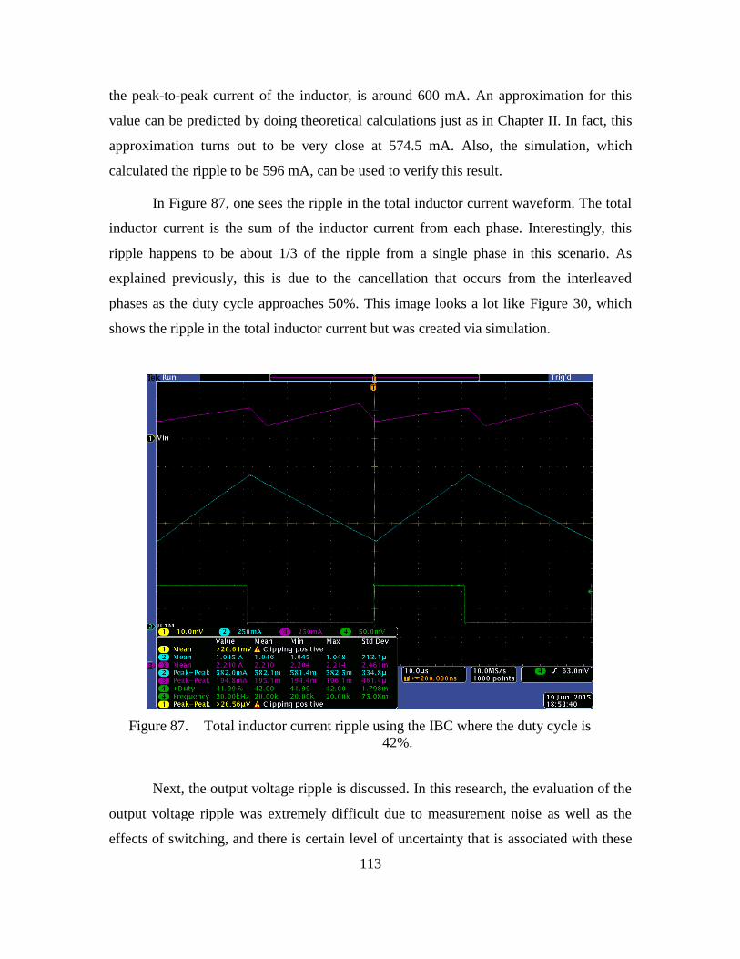
113
the peak-to-peak current of the inductor, is around 600 mA. An approximation for this
value can be predicted by doing theoretical calculations just as in Chapter II. In fact, this
approximation turns out to be very close at 574.5 mA. Also, the simulation, which
calculated the ripple to be 596 mA, can be used to verify this result.
In Figure 87, one sees the ripple in the total inductor current waveform. The total
inductor current is the sum of the inductor current from each phase. Interestingly, this
ripple happens to be about 1/3 of the ripple from a single phase in this scenario. As
explained previously, this is due to the cancellation that occurs from the interleaved
phases as the duty cycle approaches 50%. This image looks a lot like Figure 30, which
shows the ripple in the total inductor current but was created via simulation.
Total inductor current ripple using the IBC where the duty cycle is Figure 87.
42%.
Next, the output voltage ripple is discussed. In this research, the evaluation of the
output voltage ripple was extremely difficult due to measurement noise as well as the
effects of switching, and there is certain level of uncertainty that is associated with these
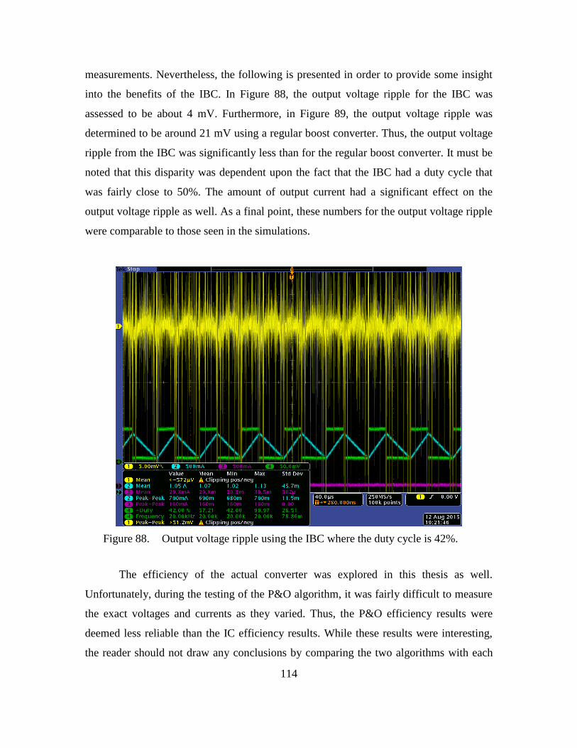
114
measurements. Nevertheless, the following is presented in order to provide some insight
into the benefits of the IBC. In Figure 88, the output voltage ripple for the IBC was
assessed to be about 4 mV. Furthermore, in Figure 89, the output voltage ripple was
determined to be around 21 mV using a regular boost converter. Thus, the output voltage
ripple from the IBC was significantly less than for the regular boost converter. It must be
noted that this disparity was dependent upon the fact that the IBC had a duty cycle that
was fairly close to 50%. The amount of output current had a significant effect on the
output voltage ripple as well. As a final point, these numbers for the output voltage ripple
were comparable to those seen in the simulations.
Output voltage ripple using the IBC where the duty cycle is 42%. Figure 88.
The efficiency of the actual converter was explored in this thesis as well.
Unfortunately, during the testing of the P&O algorithm, it was fairly difficult to measure
the exact voltages and currents as they varied. Thus, the P&O efficiency results were
deemed less reliable than the IC efficiency results. While these results were interesting,
the reader should not draw any conclusions by comparing the two algorithms with each
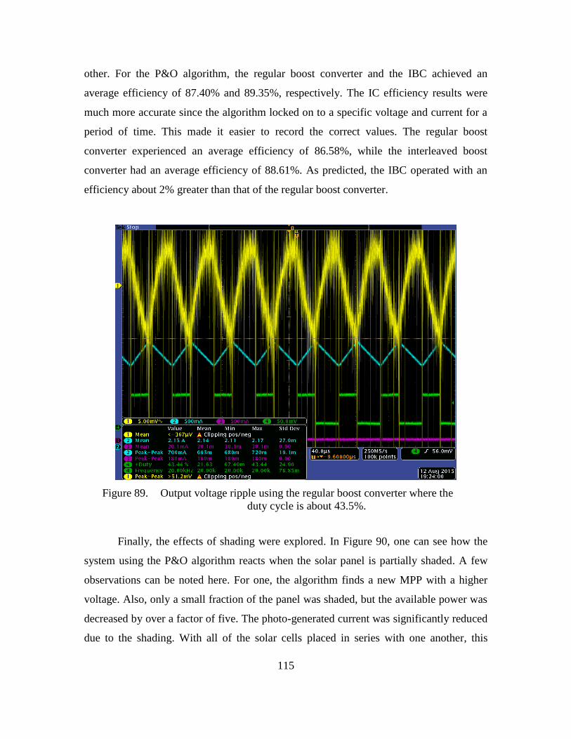
115
other. For the P&O algorithm, the regular boost converter and the IBC achieved an
average efficiency of 87.40% and 89.35%, respectively. The IC efficiency results were
much more accurate since the algorithm locked on to a specific voltage and current for a
period of time. This made it easier to record the correct values. The regular boost
converter experienced an average efficiency of 86.58%, while the interleaved boost
converter had an average efficiency of 88.61%. As predicted, the IBC operated with an
efficiency about 2% greater than that of the regular boost converter.
Output voltage ripple using the regular boost converter where the Figure 89.
duty cycle is about 43.5%.
Finally, the effects of shading were explored. In Figure 90, one can see how the
system using the P&O algorithm reacts when the solar panel is partially shaded. A few
observations can be noted here. For one, the algorithm finds a new MPP with a higher
voltage. Also, only a small fraction of the panel was shaded, but the available power was
decreased by over a factor of five. The photo-generated current was significantly reduced
due to the shading. With all of the solar cells placed in series with one another, this
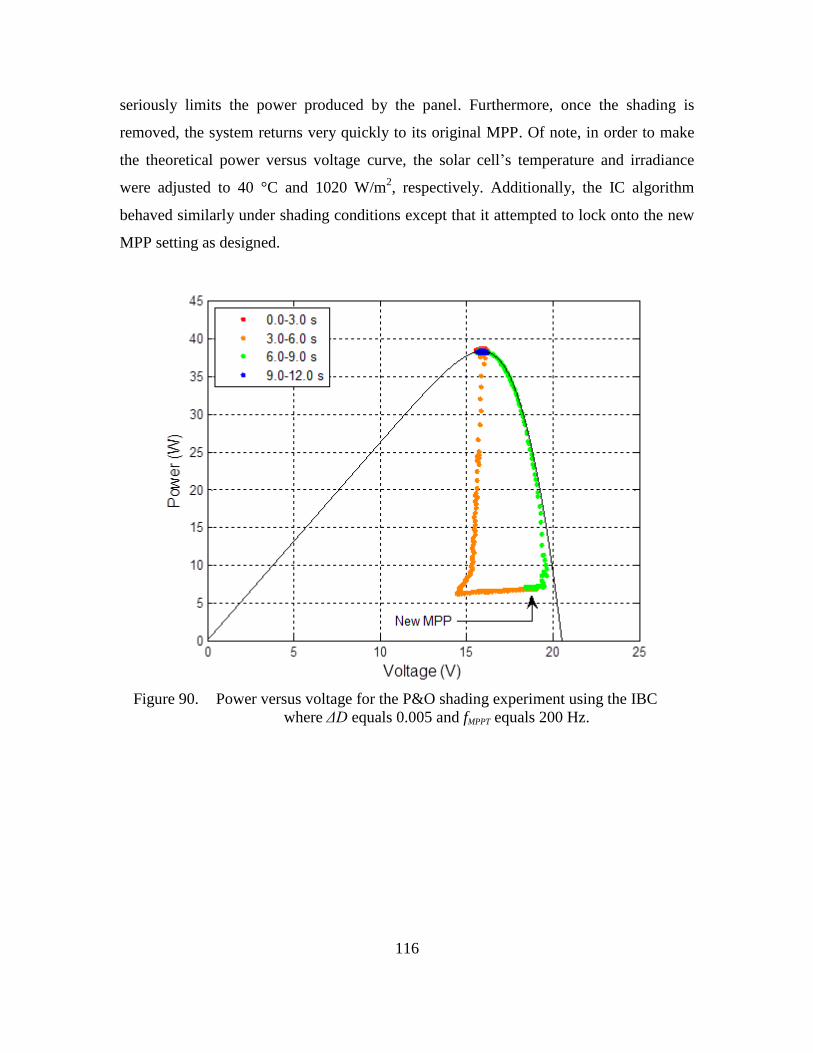
116
seriously limits the power produced by the panel. Furthermore, once the shading is
removed, the system returns very quickly to its original MPP. Of note, in order to make
the theoretical power versus voltage curve, the solar cell’s temperature and irradiance
were adjusted to 40 °C and 1020 W/m2, respectively. Additionally, the IC algorithm
behaved similarly under shading conditions except that it attempted to lock onto the new
MPP setting as designed.
Power versus voltage for the P&O shading experiment using the IBC Figure 90.
where ΔD equals 0.005 and fMPPT equals 200 Hz.

117
VI. CONCLUSIONS AND RECOMMENDATIONS
Some conclusions that were deduced from this research as well as some
recommendations for future work on this topic are offered in this chapter, which is not
intended to be all-inclusive. In fact, many of the recommendations and findings have
already been shared throughout this thesis.
A. CONCLUSIONS
In conclusion, this research was successful. The author was able to explore the
many facets of maximum power point tracking as well as the interleaved boost converter.
Also, two successful algorithms were designed and tested using the Xilinx FPGA
hardware and software. The main outcomes of this research and the associated lessons
learned are described in the following.
1. Benefits of Maximum Power Point Tracking
The main benefit of using a MPPT algorithm is that it allows the system to extract
the most power from panel vice some fraction of that. As suggested previously, without
the MPPT, the solar panel is not necessarily able to operate at its maximum power point.
This is unfortunate since a great deal of available power is potentially lost. The benefits
of tracking the MPP for each panel versus employing a centralized controller were also
explained. It was shown that connecting a converter to each panel yields more overall
power than using a system that tracks the MPP of an assembly of solar panels.
2. Benefits of using an Interleaved Boost Converter
In this thesis, the IBC was shown to offer some key benefits. For one, it operates
with greater efficiency than a regular boost converter. Additionally, the IBC produces a
lower ripple since the inductor currents have a tendency to cancel each other. Because the
IBC has more power electronic components, it likely costs more than a regular boost
converter. Furthermore, it is more complicated to control and operate when compared to
a regular boost converter.

118
3. Best MPPT Algorithm
While it would be preferred to rule that one algorithm was better than the other,
this is difficult to do. Both of the algorithms have advantages and disadvantages. For
instance, perturb and observe is a better algorithm if a simple, reliable MPPT program is
desired; however, P&O does not stabilize perfectly at the MPP but fluctuates about the
MPP. On the other hand, incremental conductance is best if one wishes to lock onto to a
specific setting, which allows the system to operate more steadily at the MPP. This
method induces almost no fluctuations in the voltage and current once it is stable at the
MPP. The IC algorithm is more complicated, so it is likely more costly to program and
implement. Additionally, as seen in this research, it was possible for the IC algorithm to
lock onto the wrong point, in which case the system does not extract the maximum power
from the solar panels.
4. Best Parameters for the Algorithm
When these algorithms are implemented on a digital platform, the MPPT rate and
the step-size for the change in duty cycle (or reference voltage) are critical parameters.
As the MPPT rate increases, the algorithm should be able to track the MPPT more
quickly under changing conditions. It must be noted that doing this may require increased
measurement resolution, or it may not be able to correctly find the MPP. Likewise,
increasing the step-size reduces the tracking time, but increased measurement resolution
may be needed. Furthermore, a large step-size can cause large fluctuations around the
MPP; thus, it is desirable to reduce the step-size to an acceptable level so that the
fluctuations in voltage and current are tolerable.
In this thesis, the best combination of settings was a MPPT frequency of 200 Hz
and a step-size for the duty cycle of 0.005. This gave the best mixture of speed and
stability in the steady-state. One can increase ΔD to get more speed, but this has a slight
drawback. For instance, as the change in duty cycle was increased to 0.01 while fMPPT
remained at 200 Hz, the amount of perturbation also increased. When using the P&O
algorithm, this causes the system to vary about the MPP a little more. When using IC, the
algorithm sometimes fluctuated very briefly until it found an appropriate setting to lock
119
on to the MPP. When fMPPT was increased to 400 Hz while keeping ΔD at 0.005, the
algorithm made its decision before the dynamics of the system had settled. One must
realize that the dynamics of the system only apply to this particular converter with its
specific components. For a different converter, a frequency of 400 Hz may not have this
issue. As a final point, the speed was cut in half when the frequency was decreased to 100
Hz.
5. Implementation Difficulty
The difficulty of implementation was another key takeaway from this research.
While developing a simulation is challenging enough, the real problem is in applying the
theory to an actual physical system. For instance, the power board was originally meant
to function as an inverter, so it had to be altered in order to work as an IBC. This
involved removing a capacitor and modifying the circuit that sent the logic signals to the
gate drivers. Once that was done, the sensors had to be calibrated so that they gave
reasonable information. The issue of noise also had to be mitigated; thus, a digital filter
was employed. It took many simulations to see what cutoff frequency worked best. Last
but not least, the control parameters for the algorithms had to be fine-tuned so that the
algorithm functioned as desired. This involved countless simulations and tests to find the
best settings.
B. RECOMMENDATIONS
Several recommendations for future work are contained in the following section.
Some of these recommendations expand upon the present research while some could
possibly develop into an entirely new research topic.
1. Create a Faster and More Accurate Simulation
The Simulink simulations took an excessively long time. For instance, the
simulation of the incremental conductance algorithm in Simulink took to 10.5 hours to
run just a 0.7 second simulation when using a 40 ns numerical step-size. Even when the
numerical step-size was increased to 250 ns, the incremental conductance simulation still
took about 1.5 hours. If the simulation was forced to run much faster, then accuracy was

120
sacrificed.; hence, it is desired to find a way to increase the speed of the simulation while
maintaining its accuracy. Also, while the modeling of the solar panel’s characteristics
was very good, it was not perfect. As one can see in Figures 80 and 82, the open-circuit
voltage did not perfectly match the real data. Perfecting the model of the solar panel
would be beneficial.
2. Optimize the Hardware
Due to the time constraints while developing this thesis, the author did not have
the time to build the hardware that was used in this research. Instead, a previously used
inverter was modified in order to create the interleaved boost converter, and there are
many items that could have been better optimized for performance. For instance, the
capacitors and inductors were too large. While this helped control the ripple, these sizes
would not be practical in a commercial product. Also, reducing the size of these
components would minimize the conduction losses associated with these items.
Furthermore, the analog-to-digital converter that was used was a 12-bit device. While this
was adequate, it would have been better too use an ADC that had better resolution in
order to achieve voltage and current measurements that were more accurate. In addition,
the IGBTs were too large and had too high of a voltage rating. A smaller device would
have made the system more efficient. For instance, using a power metal-oxide
semiconductor field-effect transistor (MOSFET) may have been a better choice instead of
IGBTs since the voltage and currents involved were small. Also, using MOSFETs would
have allowed for a higher switching frequency than using IGBTs [17]. Along the same
lines, the selection of a diode with lower on-state voltage drop would have helped
improve efficiency as well. The highest voltage that these components are required to
block is about 50 V; thus, selecting a smaller diode as well as a smaller transistor would
have been entirely reasonable.
3. Explore Other Algorithms and Scenarios
There were many maximum power point tracking algorithms presented in this
thesis. For future work, one could explore one of these other MPPT algorithms with an
interleaved boost converter. Furthermore, one could test other scenarios such as multiple

121
solar panels connected in parallel and/or series. During the testing phase of this research,
the sun was used as the sole source of solar energy. If one could obtain a solar power
simulator or a light source that could be controlled, then one could conduct scenarios
where the solar irradiance is varied precisely. Lastly, one could explore the DCM
characteristics of the IBC in detail.
4. Construct a Resonant IBC
Switching losses were a significant portion of the reduced efficiency seen in the
interleaved boost converter. Developing an IBC that attempts to avoid some or all of
these losses through resonance is a worthwhile task. One could base such a proposal off
the existing designs that incorporate resonant switching into a regular boost converter.
With that, one could add an additional phase and ensure that the gating signals were
interleaved. Alternatively, one could develop another topology that employed resonant
principles but also utilized the interleaving effect.
5. Integrate a Charge Controller
The main focus of this research was to do maximum power point tracking in order
to power a resistive load and a battery. Another thesis topic is to develop a charge
controller for the battery. This controller would integrate with the MPPT algorithm and
the IBC. In this case, the layout of the system would be almost identical except that there
would be some extra switches that would be in series with the battery and the load. There
would be some additional logic involved in order to decide whether the battery, the load,
or both would be powered according to the charge controller’s settings.

122
THIS PAGE INTENTIONALLY LEFT BLANK

123
APPENDIX A. MATLAB CODE
%% Solar model parameters
close all
sim=1; if sim==1 tstep=3.125*40e-9; % sets the time step for the clock ADC_count=round(180/3.125); % specifies the number of clock cycles
for the ADC sample period ADC_sample=ADC_count*tstep; % sets the ADC sample period ADC_freq=1/ADC_sample; % finds the ADC sample frequency f_clock=1/tstep; % sets the clock frequency Dcmtn_plot=16; % specifies the decimation for plotting else tstep=40e-9; % sets the time step for the clock ADC_count=180; % specifies the number of clock cycles for the ADC
sample period ADC_sample=ADC_count*tstep; % sets the ADC sample period ADC_freq=1/ADC_sample; % finds the ADC sample frequency f_clock=1/tstep; % sets the clock frequency Dcmtn_plot=16*3.125; % specifies the decimation for plotting end
% Analog-to-Digital Conversion parameter
f_cut_V=100; % sets the voltage cutoff frequency for the digital filter
in Hz f_cut_I=100; % sets the current cutoff frequency for the digital filter
in Hz
pre_gain_V=2*pi*f_cut_V*tstep; % calculates the pre-gain of the digital
filter for the voltage signal pre_gain_I=2*pi*f_cut_I*tstep; % calculates the pre-gain of the digital
filter for the current signal
feedback_gain_V=1-2*pi*f_cut_V*tstep; % calculates the feedback gain of
the digital filter for the voltage signal feedback_gain_I=1-2*pi*f_cut_I*tstep; % calculates the feedback gain of
the digital filter for the current signal
F_mat=[0 0 0 1;1 1 2 0;2 2 3 0;3 3 0 0]; % sets up the F matrix to be
used in the Mealy State Machine used for analog-to-digital conversion O_mat=F_mat;% sets up the O matrix to be used in the Mealy State
Machine used for analog-to-digital conversion
V_offset=-0.168; % adds an offset to the measured input voltage I_offset=0.016; % adds an offset to the measured input current V_out_offset=0.0; % adds an offset to the measured output voltage

124
V_scaling=0.9913; % multiplies a scaling factor to the measured input
voltage I_scaling=1.0384; % multiplies a scaling factor to the measured input
current
V_noise_SD=0.05; % sets the standard deviation for the voltage noise I_noise_SD_high=0.06; % sets the standard deviation for the current
noise when the current is high I_noise_SD_low=0.01; % sets the standard deviation for the current
noise when the current is low
high_to_low=0.22; % specifies when the irradiance transitions from high
to low low_to_high=0.4; % specifies when the irradiance transitions from low
to high
gain2out=1/(1/6800+1/200000)/(1/(1/6800+1/200000)+120000*2); % output
voltage sensor gain gain2=1/(1/100000+1/200000)/(1/(1/100000+1/200000)+120000*2); % input
voltage sensor gain gainI220=(3/1000*220); % current sensor gain
%Constants
k=1.3806488e-23; % Boltzmann Constant q=1.602176565e-19; % electron charge Temp_ref=25; % Reference temperature of the solar cells in Celsius Kelvin=273.15; % Temperature in Kelvin at 0 deg Celsius Dcmtn=1000; % specifies the decimation for displaying values
% Solar array parameters
Temp=50; % Actual temperature of the solar cells in Celsius S=1000; % solar insolation in W/m^2 theta=0.0*(pi/180); % angle of incidence S_rate=10000; % max rate at which the solar irradiance is allowed to
change in W/m^2 per second change_in_S=S*.8; % defines the change in S for the simulation K_i=0.0017; % amps per temperature (A/degrees) - “MATLAB/Simulink Based
Modelling of Solar Photovoltaic Cell” by Salmi et al. Eg=1.11; % bandgap energy of silicon in eV cell_area=(4+7/8)*(2+7/16)*(2.54)^2; % cell area in cm^2 Jsc=0.0331325; % short circuit surface current density in A/cm^2 Isc=Jsc*cell_area; % short circuit current of the solar cell at a solar
irradiance of 1000 W/m^2 and a temperature of 25 degrees C Rsh=1000; % Shunt resistance for solar cell model Rs=0.01717; % Series resistance for solar cell model Is_ref=3.12e-8; % reverse saturation current at 25 degrees C Is2_ref=0; % Set to zero for 1-diode model; otherwise, set as
appropriate for 2-diode model N1=1.282; % Ideality factor N2=1.2; % Used only in the 2-diode model Cell_series=36; % number of cells in series per module Cell_parallel=1; % number of cells in parallel per module

125
Module_series=1; % number of modules in series per array Module_parallel=1; % number of modules in parallel per array
% Converter parameters
fs=20e3; % switching frequency of the switches Cpv=650e-6; % Capacitance of the PV capacitor Vin_IC=19.77; % Initial input voltage for the PV capacitor L=470e-6; % Inductance of the inductor RL=0.25; % Resistance of the inductor C=990e-6; % Capacitance of the output capacitor Vout_IC=23.77; % Initial output voltage for the output capacitor f_cut=1/(2*pi*sqrt(L*C)); % Cutoff frequency in Hz R_diode=0.15; % sets the diode resistance R_IGBT=0.15; % sets the IGBT resistance Vf_diode=0.6; % sets the diode forward voltage drop Vf_IGBT=1.2; % sets the IGBT forward voltage drop
Cs_MOSFET=1e-15; % sets snubber parameters so that there is effectively
no snubber in the simulated circuit Rs_MOSFET=1e15; Cs_IGBT=1e-15; Rs_IGBT=1e15; Cs_diode=1e-15; Rs_diode=1e15;
% Load parameters
Rload=18.23; % specifies the load resistance Lload=0; % specifies the load inductance Rbatt=0.175; % source resistance (substitute for the battery) Vbatt=24; % specifies the battery voltage
% Duty cycle parameters
MnPrd=1/fs; % specifies the mean period for averaging certain signals D_IC=0.25; % specifies the initial condition for the duty cycle D_lower=0.05; % specifies lowest allowable duty cycle D_upper=0.95; % specifies highest allowable duty cycle number_of_interleave=2; % specifies the number of interleaved parallel
branches interleave_delay=round(((1/fs)/number_of_interleave)/tstep); %
determines the interleaved delay in number of clocks
% MPPT control paramters
T_sample=1/200; % sampling period of the MPPT in seconds MPPT_delay=round(T_sample/tstep); % number of clock cycles associated
with the Delay for MPPT delta_D=0.005; % step-size for change in duty cycle IC_limit=0.012; % sets the limit for abs(dI/dV+I/V) to be considered 0 IC_limit_dV=0.007; % sets the limit for abs(dV) to be considered 0 IC_limit_dI=0.006; % sets the limit for abs(dI) to be considered 0

126
% Xilinx parameters
bits=23; % specifies the number of bit to be used for fixed point
numbers bp=17; % specifies the binary point location for fixed point numbers step_bits=34; % specifies the number of bit to be used to represent the
step size for fixed point numbers accum_bits=59; % specifies the number of bit to be used in the
accumulator for fixed point numbers const_bits=21; % % specifies the number of bit to be used to express
certain constants bits1=bp+1; % specifies the number of bit to be used as bp+1 bits2=bp+2; % specifies the number of bit to be used as bp+2 bits3=bp+3; % specifies the number of bit to be used as bp+3 bits4=bp+4; % specifies the number of bit to be used as bp+4 MPPT_bits=22; % defines the number of bit to use for the MPPT counter PWM_bits=12; % defines the number of bit used to count for the PWM
signal ADC_count_bits=8; % specifies number of bits to use for the ADC counter data_rate_count=round((12/2^12)/tstep); % specifies the number of clock
cycles for the data rate into Chipscope; do not make greater than 2^17
without adding more bits data_rate_bits=17; % specifies number of bits to use for the data rate
counter
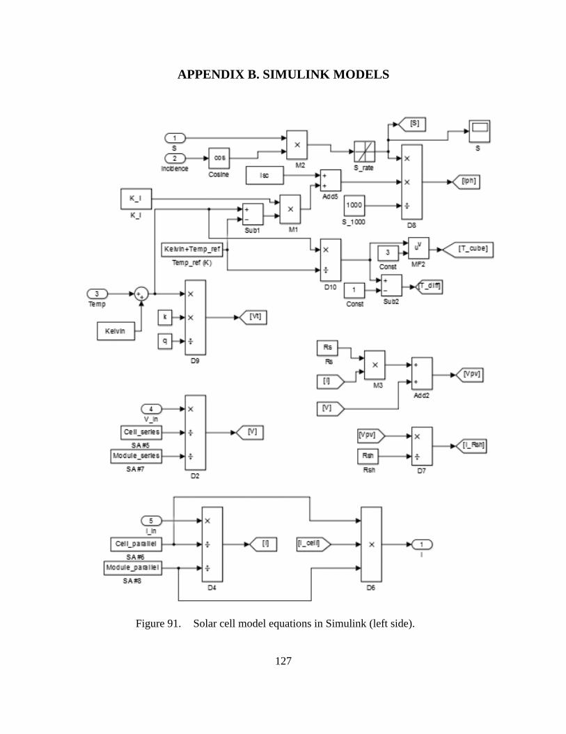
127
APPENDIX B. SIMULINK MODELS
Solar cell model equations in Simulink (left side). Figure 91.
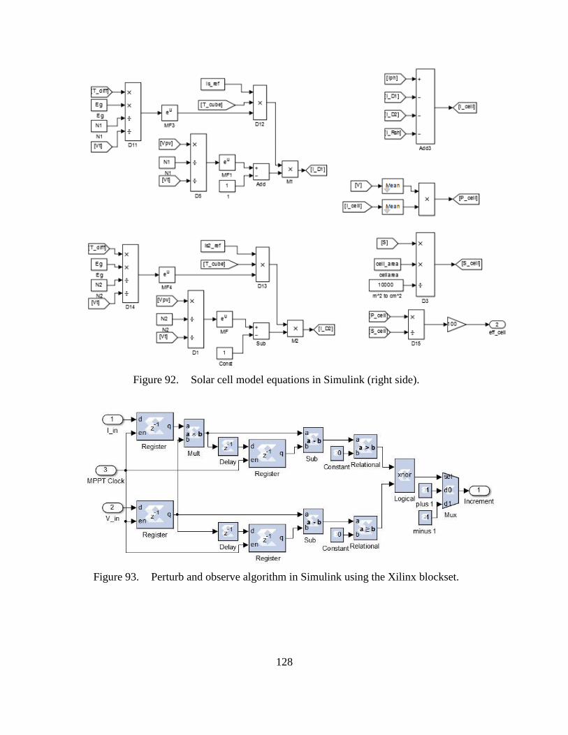
128
Solar cell model equations in Simulink (right side). Figure 92.
Perturb and observe algorithm in Simulink using the Xilinx blockset.Figure 93.
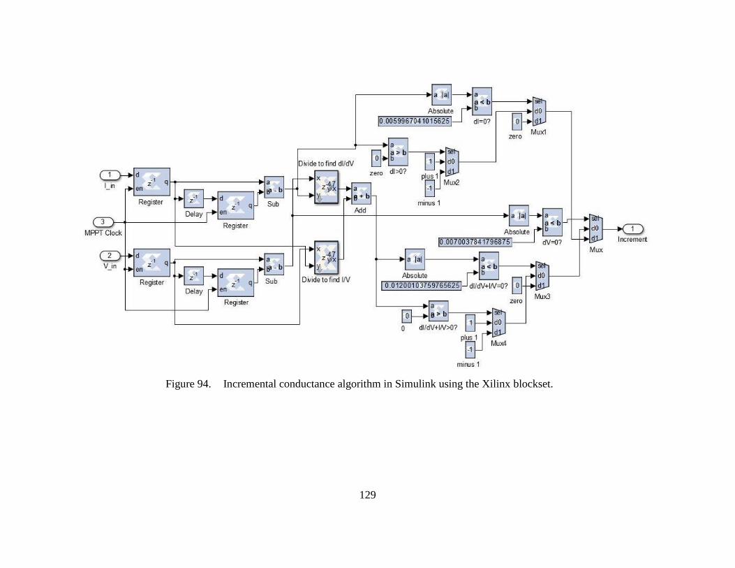
129
Incremental conductance algorithm in Simulink using the Xilinx blockset.Figure 94.

130
Saturation limits in Simulink using the Xilinx blockset Figure 95.
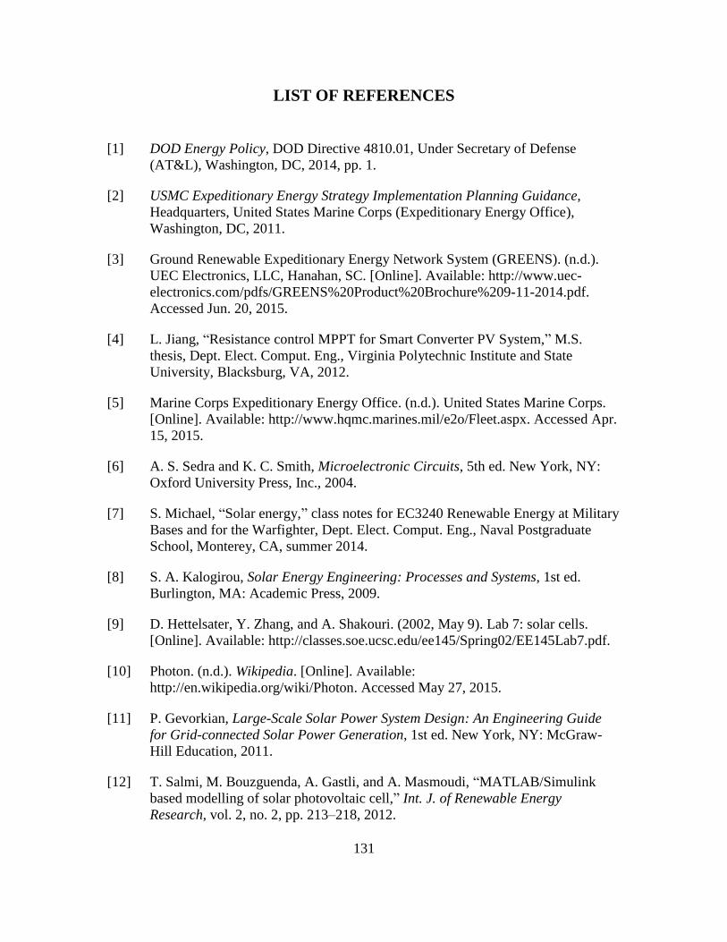
131
LIST OF REFERENCES
[1] DOD Energy Policy, DOD Directive 4810.01, Under Secretary of Defense
(AT&L), Washington, DC, 2014, pp. 1.
[2] USMC Expeditionary Energy Strategy Implementation Planning Guidance,
Headquarters, United States Marine Corps (Expeditionary Energy Office),
Washington, DC, 2011.
[3] Ground Renewable Expeditionary Energy Network System (GREENS). (n.d.).
UEC Electronics, LLC, Hanahan, SC. [Online]. Available: http://www.uec-
electronics.com/pdfs/GREENS%20Product%20Brochure%209-11-2014.pdf.
Accessed Jun. 20, 2015.
[4] L. Jiang, “Resistance control MPPT for Smart Converter PV System,” M.S.
thesis, Dept. Elect. Comput. Eng., Virginia Polytechnic Institute and State
University, Blacksburg, VA, 2012.
[5] Marine Corps Expeditionary Energy Office. (n.d.). United States Marine Corps.
[Online]. Available: http://www.hqmc.marines.mil/e2o/Fleet.aspx. Accessed Apr.
15, 2015.
[6] A. S. Sedra and K. C. Smith, Microelectronic Circuits, 5th ed. New York, NY:
Oxford University Press, Inc., 2004.
[7] S. Michael, “Solar energy,” class notes for EC3240 Renewable Energy at Military
Bases and for the Warfighter, Dept. Elect. Comput. Eng., Naval Postgraduate
School, Monterey, CA, summer 2014.
[8] S. A. Kalogirou, Solar Energy Engineering: Processes and Systems, 1st ed.
Burlington, MA: Academic Press, 2009.
[9] D. Hettelsater, Y. Zhang, and A. Shakouri. (2002, May 9). Lab 7: solar cells.
[Online]. Available: http://classes.soe.ucsc.edu/ee145/Spring02/EE145Lab7.pdf.
[10] Photon. (n.d.). Wikipedia. [Online]. Available:
http://en.wikipedia.org/wiki/Photon. Accessed May 27, 2015.
[11] P. Gevorkian, Large-Scale Solar Power System Design: An Engineering Guide
for Grid-connected Solar Power Generation, 1st ed. New York, NY: McGraw-
Hill Education, 2011.
[12] T. Salmi, M. Bouzguenda, A. Gastli, and A. Masmoudi, “MATLAB/Simulink
based modelling of solar photovoltaic cell,” Int. J. of Renewable Energy
Research, vol. 2, no. 2, pp. 213–218, 2012.
132
[13] S. Nema, R. K. Nema, and G. Agnihotri, “MATLAB/Simulink based study of
photovoltaic cells / modules / array and their experimental verification,” Int. J. of
Energy and Environment, vol. 1, no. 3, pp. 487–500, 2010.
[14] H. Tsai, C. Tu, and Y. Su, “Development of generalized photovoltaic model using
MATLAB/SIMULINK,” in Proc. of the World Congr. on Eng. and Comput. Sci.,
San Francisco, CA, 2008, pp. 1–6.
[15] Shanghai Raloss Energy Technology Co., Ltd. (2007, Sep.). RLS-Datasheet-1.
Shanghai, China. [Online]. Available:
http://www.farnell.com/datasheets/95510.pdf.
[16] R. Ashton, “Popular direct-coupled dc-dc converters,” class notes for EC3150
Solid State Power Conversion, Dept. Elect. Comput. Eng., Naval Postgraduate
School, Monterey, CA, summer 2014.
[17] N. Mohan, T. M. Undeland, and W. P. Robbins, Power Electronics: Converters,
Applications, and Design, 3rd ed. Hoboken, NJ: John Wiley & Sons, Inc., 2003.
[18] P. T. Krein, Elements of Power Electronics, 1st ed. New York, NY: Oxford
University Press, Inc., 1997.
[19] B. Hauke, “Basic calculation of a boost converter’s power stage,” Texas
Instruments Inc., Dallas, TX, App. Rep. SLVA372C, Jan. 2014.
[20] R. Crews, “AN-1820 LM5032 interleaved boost converter,” Texas Instruments
Inc., Dallas, TX, App. Rep. SNVA335A, May 2013.
[21] H. M. Mallikarjuna Swamy, K. P. Guruswamy, and S. P. Singh, “Design,
modeling and analysis of two level interleaved boost converter,” in Int. Conf. on
Mach. Intell. Res. and Advancement, Katra, India, 2013, pp. 509–514.
[22] A. Dolara, R. Faranda, and S. Leva, “Energy comparison of seven MPPT
techniques for PV systems,” J. Electromagnetic Analysis & Applications, no. 3,
pp. 152–162, Sep. 2009.
[23] D. Ragonese and M. Ragusa, “Designing with the SPV1020, an interleaved boost
converter with MPPT algorithm,” STMicroelectronics, Geneva, Switzerland, App.
Note AN3392, May 2012.
[24] S. Gomathy, S. Saravanan, and S. Thangavel, “Design and implementation of
Maximum Power Point Tracking (MPPT) Algorithm for a Standalone PV
System,” Int. J. of Scientific & Eng. Res., vol. 3, no. 3, pp. 428–434, Mar. 2012.
[25] T. Esram and P. Chapman, “Comparison of photovoltaic array maximum power
point tracking techniques,” IEEE Trans. Energy Convers., vol. 22, no. 2, pp. 439–
449, Jun. 2007.

133
[26] R. Faranda and S. Leva, “Energy comparison of MPPT techniques for PV
systems,” WSEAS Transactions on Power Systems, vol. 3, no. 6, pp. 446–455,
Jun. 2008.
[27] M. A. Gomes de Brito, L. Galotto, Jr., L. P. Sampaio, G. de Azevedo e Melo, and
C. A. Canesin, “Evaluation of the main MPPT techniques for photovoltaic
applications,” IEEE Trans. Ind. Electron., vol. 60, no. 3, pp. 1156–1167, Mar.
2013.
[28] D. Shmilovitz, “On the control of photovoltaic maximum power point tracker via
output parameters,” in IEEE Proc. Elect. Power Appl., vol. 152, no. 2, pp. 239–
248, Mar. 2005.
[29] F. Blaabjerg, Z. Chen, and S. B. Kjaer, “Power electronics as efficient interface in
dispersed power generation systems,” IEEE Trans. Power Electron., vol. 19, no.
5, pp. 1184–1194, 2004.
[30] C. A. Stephenson, “Utilizing maximum power point trackers in parallel to
maximize the power output of a solar (photovoltaic) array,” M.S. thesis, Dept.
Elect. Comput. Eng., Naval Postgraduate School, Monterey, CA, 2005.
[31] Diodes in PV systems. (n.d.). OkSolar.com. [Online]. Available:
http://www.oksolar.com/technical/diodes_in_pv_systems.htm. Accessed Aug. 10,
2015.
[32] Diodes in solar arrays. (2001). ABS Alaskan, Inc., Fairbanks, AK. [Online].
Available: http://www.absak.com/tech/diodes.pdf.
[33] R. Regan. (2012, Dec. 13). Number of bits in a decimal integer. [Online].
Available: http://www.exploringbinary.com/number-of-bits-in-a-decimal-integer/
[34] C. L. Phillips and H. T. Nagle, Digital Control System Analysis and Design, 3rd
ed. Englewood Cliffs, NJ: Prentice-Hall, Inc., 1995.
[35] The MathWorks, Inc. (2015). SimPowerSystems. [Online]. Available:
http://www.mathworks.com/products/simpower/

134
THIS PAGE INTENTIONALLY LEFT BLANK

135
INITIAL DISTRIBUTION LIST
1. Defense Technical Information Center
Ft. Belvoir, Virginia
2. Dudley Knox Library
Naval Postgraduate School
Monterey, California