Embed Size (px)
Citation preview
REVIEW OF SCIENTIFIC INSTRUMENTS VOLUME 74, NUMBER 11 NOVEMBER 2003
Measurement of the infrared magneto-optic properties of thin-film metalsand high temperature superconductors
J. Cernea)
Department of Physics, University at Buffalo, The State University of New York, Buffalo, New York 14260and Department of Physics, University of Maryland, College Park, Maryland 20742
D. C. SchmadelDepartment of Physics, University of Maryland, College Park, Maryland 20742
L. B. RigalLaboratoire National des Champs Magne´tiques Pulse´s, Toulouse, France and Department of Physics,University of Maryland, College Park, Maryland 20742
H. D. DrewDepartment of Physics, University of Maryland, College Park, Maryland 20742 and Centerof Superconductivity Research, University of Maryland, College Park, Maryland 20742
~Received 22 May 2003; accepted 16 July 2003!
A sensitive polarization modulation technique uses photoelastic modulation and heterodynedetection to simultaneously measure the Faraday rotation and induced ellipticity in light transmittedby semiconducting and metallic samples. The frequencies measured are in the midinfrared andcorrespond to the spectral lines of a CO2 laser. The measured temperature range is continuous andextends from 35 to 330 K. Measured samples include GaAs and Si substrates, gold and copper films,and YBCO and BSCCO high temperature superconductors. ©2003 American Institute of Physics.@DOI: 10.1063/1.1619582#
ectin-
-
esnicuid
encth
frochsin
urw
s
her
unc-
ar-nd
re a
tion,andon-
res
ical
po-t atthe
-eamthelar-mi-this
I. INTRODUCTION
Conventional dc Hall effect measurements in novel eltronic materials such as high temperature superconduccuprates~HTSC! have been essential in revealing the uusual character of these systems.1 Extending these measurements to higher frequencies2,3 allows one to probe more effectively the energy scales of the system~e.g., plasmafrequency, cyclotron frequency and carrier relaxation rat!,and provides greater insight into the intrinsic electrostructure of systems ranging from conventional Fermi liqmetals4 to more exotic metals such as HTSC~Ref. 5! andother transition metal oxides.6
Magnetopolarimetry measurements can be used totend Hall effect measurements into the infrared frequerange (1013 Hz). These measurements are sensitive tocomplex Faraday angleuF , which is closely related to thecomplex Hall angleuH .7 ThoughuF anduH tend to be smallfor metals in the midinfrared~MIR, 900– 1100 cm21), thereare a number of advantages in performing these higherquency measurements. First, the high frequency allowsto avoid impurity scattering or grain boundary effects, whimay dominate lower frequency Hall measurements. Thiespecially important in new materials, which often contamany impurities and defects. Furthermore, the MIR measments allow one to examine the trends observed at lofrequencies. Since tanuH ~and uH) obeys a sum rule,3 it isvery useful to be able to integrateuH to higher frequencies toverify whether~and where! the Hall angle sum rule saturate
a!Electronic mail: [email protected]
4750034-6748/2003/74(11)/4755/13/$20.00
Downloaded 29 Nov 2004 to 129.2.40.89. Redistribution subject to AIP
-ng-
x-ye
e-ne
is
e-er
or whether there is more relevant physics at even higfrequencies. Finally, since the high frequency behavior ofuH
is constrained by the general requirements of response ftions, a simple, model-independent asymptotic form foruH
becomes more accurate at higher frequencies.In this article, we present a sensitive midinfrared pol
imetry technique, which uses photoelastic modulation aheterodyne detection, and which can be used to explovariety of materials.8,9 In what follows, we shall first intro-duce the hardware components and describe their operanext we shall present an analysis of both the operationdata, and finally, we shall present recent results on semicductors, metal films, and HTSC.
II. EXPERIMENTAL SYSTEM
A. Overview
The experimental system of the current work measuthe real and imaginary parts ofuF using a linearly polarizedCO2 laser beam. Figure 1 schematically illustrates the optpath in which linearly polarized light from the CO2 laser,after encountering various steering and attenuation comnents, proceeds through lens 1, which focuses it to a pointhe chopper. The chopper impresses onto the intensity ofbeam a temporal square wave modulation off 0'112 Hz,which will later facilitate the removal of laser power variations using ratios. Lens 2 then refocuses the emerging bso as to eventually produce a focused diffraction spot onsurface of the sample. The intervening element, a film poizer, purifies the beam’s polarization, removing any contanation caused by the chopper, attenuators, etc. It is
5 © 2003 American Institute of Physics
license or copyright, see http://rsi.aip.org/rsi/copyright.jsp
glemeit
arota
ityrireg
r-
ue
ttorng
m-the
e
ei-
o-s is
are
odu-
IIa
ationsla-
s ac-
tri-Hz
achngsella-or
s
orning
ghng-
Aofw-ch
sult
tlly
scti
4756 Rev. Sci. Instrum., Vol. 74, No. 11, November 2003 Cerne et al.
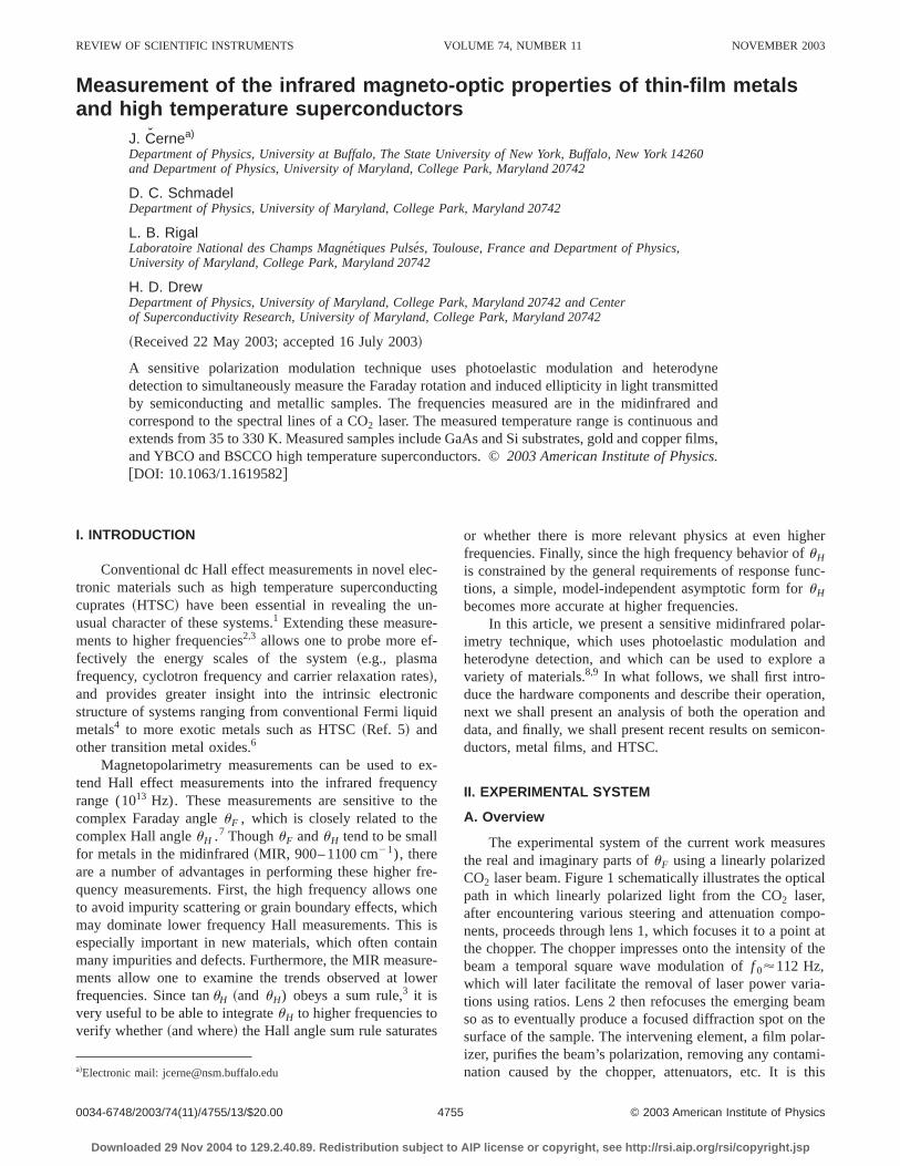
highly linearly polarized beam, which after passing throuthe ZnSe magnet housing window encounters the sampshown in Fig. 2. The sample will reflect, absorb, and transportions of this beam. The polarization of the transmittbeam will have sustained a Faraday rotation and ellipticproportional to the magnetic fieldB and consistent with thephysics peculiar to the sample. We shall assign thex axis tothe initial polarization direction and thez axis to the direc-tion of propagation.
The Faraday angle includes both real and imaginterms. The real term corresponds to a simple geometric rtion of the polarization vector about the direction of propgation. The imaginary term relates directly to the ellipticof the polarization. Since the sample is axially symmetalong B, the transmittance tensor is diagonal when repsented in the circular polarization basis. Therefore, chan
FIG. 1. Overall schematic of the optical path. The dotted line representsCO2 laser beam. The CO2 laser and the first four optic elements are actualocated on a separate mount detached from the optical table.
FIG. 2. Wedged sample and beam path. The paths of the reflected beamsufficiently separated by the 2° wedge to prevent their entering the detesystem or reentering the laser.
Downloaded 29 Nov 2004 to 129.2.40.89. Redistribution subject to AIP
hasitdy
ya--
c-
es
in the incident polarization only depend on:~1! the relativedifference in the phase of left versus right circularly polaized light due to Re(uF), which leads to a rotation@circularbirefringence or Faraday rotation~FR!# in the linearly polar-ized incident light; and~2! the relative difference in thetransmission of left versus right circularly polarized light dto Im(uF), which introduces ellipticity@circular dichroism~CD!# to the linearly polarized incident light.
The magnitude ofuF at CO2 wavelengths is abou1024 rad. As such, one may consider the electric vecalong they axis to be a feeble signal added to the strosignal of the original electric field vector along thex axis.This small signal cannot be measured directly by the comon method of crossed polarizers because the power infield polarized along they axis is proportional to the squarof uF or 1028 times the power in the original beam in thexpolarization. Clearly, leakage of the input beam throughther polarizer would effectively direct power into they axispolarization, which would overwhelm any amount intrduced by the sample. The natural choice in such instanceheterodyne detection.
Heterodyne detection produces cross terms, whichproportional to the electric vector along they axis rather thanits square. We realize heterodyne detection by phase mlating the electric vector along they axis using a photoelasticmodulator ~PEM!. The PEM is a model PEM-90 seriesZS50 manufactured by Hinds Instruments, Inc., withmodulation frequency off m550 kHz ~angular frequencyvm52p f m). It comprises essentially a block of ZnSe andpiezoelectric transducer, which creates the stress alternaat a frequency of 50 kHz and ultimately the phase modution of the light beam. The electric vector along thex axis isessentially unaffected by the PEM.
The beam emerges from the PEM and then strikepolarizer on a 45° angle, which allows a portion of the eletric vector from each of they andx directions to contributeto that which emerges now at a 45° angle. These two conbutions after being mixed by the detector produce the 50 kPEM frequency along with sidebands. The amplitude of eof the sidebands is proportional to the electric vector alothe y axis and also proportional to the corresponding Besfunction, whose argument is the depth of the PEM modution. In fact, as will be derived below, the even sidebandsharmonics are proportional to Re(uF) and the odd sidebandor harmonics are proportional to Im(uF).
In the following sections we consider certain elementssubassemblies of the experimental system in detail beginwith the CO2 laser.
B. CO2 laser
The CO2 laser, a model PL5 manufactured by EdinburInstruments, Ltd., provides a number of spectral lines raing from 9.174 to 10.860mm ~1090 to 920 cm21), any oneof which is selected by a grating internal to the cavity.separate CO2 laser spectrometer verifies the wavelengtheach line. The direction of the beam exiting the laser, hoever, differs for different lines sometimes by nearly as muas one half of a spatial mode. Without realignment the re
he
areon
license or copyright, see http://rsi.aip.org/rsi/copyright.jsp

pleuuspt
innct
arginhte
uea
uminreue
se
rnnaa-ccceerati
la
pleenthth
onngpheamerdath
dif-at aededTheef-a
pingd in
icketm-rcesrge,ul-
on-he
t 9,heethely
isheheiv-ro-userierhinorehisrier
es-ten-
4757Rev. Sci. Instrum., Vol. 74, No. 11, November 2003 Thin-film magneto-optic properties
would be a spatial shift of the diffraction spot at the samby as much as one half of a spot diameter. The small siza sample can aggravate the sensitivity of the system to sslight misalignment particularly when such changes cathe beam to wander off or even near the edge of the samLens 3 essentially focuses an image of the sample ontoiris shown in Fig. 1 and may be used as an aid in regainalignment as is necessary to compile valid relative frequedata. The design and construction of the hardware ensurethe relative position of the sample, lens 3, and the irisconstant. Therefore, adjusting the laser beam steerinmaximize the power through the iris after each laser lchange likewise ensures that the beam is passing througsame area of the sample. While taking data, the iris is dilato accommodate a small amount of beam wander.
Another consideration of the laser is the high outppower ~2–30 W!. Three attenuators reduce the pow;30 dB to avoid heating the sample while still producingstrong signal within the linear range of the mercury cadmitelluride ~MCT! detector. These attenuators are ZnSe wdows having an antireflection coating on one side. Theyplace mirrors in the beam steering assemblies with thecoated side serving as the reflective surface. Each of thattenuators introduces approximately 10 dB of loss.
To reduce noise due to temporal fluctuations in the laoutput power, the Faraday signals at harmonics ofvm arenormalized by the laser power level, which is sampled atv0 .The current experiment employs the usual method of soucompensation,10 which involves the chopper along with aadditional lock-in amplifier. Note, also, that the heterodydetection system described above permits use of the sdetector for the power level sample as well as the secondthird harmonics ofvm . This feature eliminates the wavelength dependence of the detector, and thus facilitates arate relative measurements of the wavelength dependenthe complexuF . A final consideration regarding the lasinvolves its placement with respect to the magnet. The pticular position of the laser is perpendicular to the magnefield and at such a distance as to reduce detuning of thecavity caused by magnetostriction to a tolerable amount.
C. Magnet system and sample mounting
The optical magnet system~an 8 T, split coil, HelmholtzSpectromag, manufactured by Oxford Instruments PLC! in-volved a side-loading sample cold finger, with the samlocated in vacuum. Therefore, no cold windows are requirwhich proved to be advantageous for these measuremThe main modifications to the magnet system involvedexternal windows, the sample handling hardware, andinternal bore tube shielding. To understand the modificatito the external windows, consider that the wavelength raof interest requires ZnSe windows. However, the band gaZnSe is only 2.7 eV, and the magnetic field of 2 T at toriginal location of the windows caused a significant Faradrotation, which overwhelmed that of the sample. The 35-clong aluminum extension tubes locate the windows whthe magnetic field is less than 0.1 T. The remaining Fararotation background is thus reduced to the same order as
Downloaded 29 Nov 2004 to 129.2.40.89. Redistribution subject to AIP
eofchele.hegy
hatetoethed
tr
--
n-se
r
ce
emend
u-of
r-cser
ed,ts.eese
of
y-eyat
of the sample, and having been carefully measured forferent wavelengths, can be easily removed from the datalater time. For magnets requiring cold windows locatwithin the high field region the background may be reducby using a material with a higher band gap such as BaF.sample handling hardware was extensively modified. Thefort included adding a steady pin and vise, implementingmore responsive temperature control system, and develoa near stress-free sample mount. The steady pin, depicteFig. 3 protrudes from the blade of the original sample stto which it is brazed. The vise, located within the magnhousing, engages the pin using a Teflon collet. This cobined apparatus restrains the sample stick against the foinduced by the magnetic field, and thus prevents the laextraneous interference signals resulting from changing mtipaths and e´talons.
Figure 3 also depicts parts of the new temperature ctrol system, which comprises a heater and a cooling link. Theater is a 400V 1
4 W metal film resistor potted into thecopper sample carrier using 2850FT epoxy with catalysboth of which are manufactured by Emerson & Cuming. Tcooling link is simply a 4 cmlength of 22 gauge copper wirconnecting the copper sample carrier to the blade oforiginal sample stick from which it is otherwise thermalinsulated by spacers and nylon screws. The operationsimple: Liquid helium delivered to the sample stick by toriginal provision, cools the blade to about 10 K, and tcooling link cools the copper sample carrier. Current delered to the resistor in an easily controlled fashion can pvide up to 2 W of heat to the copper sample carrier. Becaof the low thermal mass of both the copper sample carand the link, a compromise temperature emerges witabout 1 min. Sweeping the temperature entails nothing mthan adjusting the current. An important advantage of tsystem is that only the rather small copper sample carchanges temperature. The remaining hardware, remainingsentially constant in temperature, has a greatly reduced
FIG. 3. Sample mount assembly.
license or copyright, see http://rsi.aip.org/rsi/copyright.jsp
o
hoivc-lerl
glearteheb
rov
Itas
ho
iooth
thbetioe
et
eremppatngthios
nodithai
cieatr
ftersessed.anthe
astiv-n
usar-wnach
atAthe
n.la-ant
nd,
teof
tor
M,gnaldblebe-
to
r-k-in
eo
res of
thefer-t of
tare
4758 Rev. Sci. Instrum., Vol. 74, No. 11, November 2003 Cerne et al.
dency to adversely affect the measurement by movingwarping.
The near stress-free sample mount consists of a pphor bronze wire retaining spring and a thermally conductflexible silver-filled RTV known as Eccobond 59C manufatured by Emerson & Cuming, Inc. The particular sampshown attached to the sample stick is a small irregulashaped film of optimally doped Bi2Sr2Ca1Cu2O81d approxi-mately 200 nm thick, which had been peeled from a sinbulk crystal. This small film was placed against a polishsurface of a BaF crystal, which serves as a substratemaintains the temperature of the sample. Van der Waal foholds the film in place. A 2° wedge of the BaF substraeliminates e´talon effects. Only one of the two corners of thsubstrate is cemented to the copper sample carrier. The pphor bronze retaining spring lightly holds the other cornwhile allowing some motion to relieve the stress causeddissimilar thermal expansion coefficients. Without this pvision the stress induced in the substrate had caused owhelming and unpredictable complex Faraday rotations.this stress-free mounting which actually facilitated the ftemperature scans required to eliminate 1/f noise apparent inprevious work. The copper sample carrier is provided witsmall fiducial hole, also shown in Fig. 3. Prior to insertionthe sample stick into the magnet the sample’s positionaccurately measured with respect to this hole. After insertthe fiducial hole is located using the transmitted intensitythe laser beam. The sample is then positioned withinbeam by raising or lowering the magnet and slidingsample stick in or out. Finally, the new reentrant bore tuare fitted with graphite plates to absorb the stray radiascattered from the incident laser beam by the various refltive surfaces, e.g., sample, substrate, magnet windows,
D. Optical table components
The remaining items of Fig. 1, which along with thmagnet are located on an aluminum optical table, willceive consideration within this section. Among these iteare the chopper and lens 1. As explained earlier, the choimpresses upon the beam a square wave amplitude variof f 05112 Hz. Lens 1 participates in this task by focusithe beam to a point at the chopper blades, otpimizingsharpness of the modulation. This prevents spatial variatwithin the beam from causing phase and amplitude errorthe reported laser power level.
Also of particular importance is a pivot platform upowhich sits the optical detection system. Two aluminum bbeams connect this platform to a vertical pivot locatedrectly below the sample. When the two clamps securingplatform to the optical table are loosened the platform mbe rotated about the vertical axis of the pivot. This motionnecessary to align the detection system to both the fiduhole and wedged substrates, which bend the laser babout the same axis by an amount depending on the subswedge angle and its index of refraction.
Downloaded 29 Nov 2004 to 129.2.40.89. Redistribution subject to AIP
r
s-e
y
edndcee
os-ry-er-ist
afisn,fe
esnc-c.
-ser
ion
ensin
x-eysalm
ate
E. Optical detection system
The first component encountered by the laser beam aexiting the second magnet window is lens 3, which focuan image of the sample onto the iris as previously discusThis lens joins with the PEM and polarization analyzer inassembly, which can be rotated as a single unit aboutinput optical axis, which is thez axis. Such a rotation isequivalent to a real, but opposite, Faraday rotation, at lefor sufficiently small angles so that the polarization sensitity of the MCT detector is not apparent. Fixed calibratiorotation stops limit this rotation to a known amount, thserving as a Faraday rotation calibrator. To calibrate the Faday rotation signal, one rotates the assembly the knoamount and uses this to scale the empirical values for ewavelength, as will be discussed in Sec. III D.
Another important consideration involves reflectionthe surfaces of the ZnSe interaction block of the PEM.reflected beam, which makes additional passes throughZnSe interaction block, will receive additional modulatioSince, the cross term is a function of the depth of modution, such triply modulated stray beams can cause significerrors. An antireflection~AR! coating and a tilting of thePEM by 25° reduce and displace reflected beams athereby, sufficiently reduce their effect.
A variable selection of polyimide films further attenuathe laser beam so that its power is within the linear rangethe MCT detector, which is a model J15D14 MCT detecmanufactured by EG&G Judson.
F. Electronic instrumentation
Along with the electronics that attend the magnet, PEchopper, etc., the system uses three model 7260 digital siprocessing~DSP! harmonic lock-in amplifiers manufactureby EG&G. These lock-ins detect the voltage of a selectaharmonics of the input signal. This feature is essentialcause, as mentioned, the even harmonics ofvm are propor-tional to Re(uF) and the odd harmonics are proportionalIm(uF). The first lock-in determines the rms voltageV0 at thechopper frequencyv0 and is considered to be the dc refeence reflecting the average laser power. The second locdetermines the rms voltageV2 at 2vm , while the third de-termines the rms voltageV3 at 3vm . These three signals arrecorded in real time by a local computer, which forms twnormalized, dimensionless signalsS2 andS3 , as shown be-low:
S25V2
V0, S35
V3
V0. ~1!
Since motion of the beam within the PEM apertuchanges the phase of the harmonics, only the magnitudeV2 andV3 are used in the signal analysis. UnlikeV2(t) andV3(t), which are sinusoidal functions,V0(t) is a squarewave and, therefore, its amplitude will be undervalued byDSP lock-in. Since the DSP lock-in uses a sinusoidal reence, it only senses the fundamental harmonic componenthe square wave.11 To correct this error, theV0 signal ismultiplied by 4/p, which is the factor that relates the firsharmonic of a square wave to the amplitude of the squwave. There are two reasons for usingS3 instead ofS1 ~the
license or copyright, see http://rsi.aip.org/rsi/copyright.jsp

t-M
ls
loanny
gm
tn
ba
e
mle
e.e
toa
in-
bylylar
therel-as
in
als am-
seof
r
4759Rev. Sci. Instrum., Vol. 74, No. 11, November 2003 Thin-film magneto-optic properties
signal at the fundamental frequencyvm), despite the fact thaS1 is typically larger thanS3 and provides the same information. S1 is more susceptible to electronic noise from the PEpower supply and transducers, which operate atvm . Further-more, the thickness of the PEM’s ZnSe optical head is amodulated atvm , causing an e´talon interference modulationsignal at the fundamental frequency.S2 andS3 will be usedto determine Re(uF) and Im(uF), respectively, as will beshown in Sec. III A.
III. ANALYSIS
In the analysis of both the system and data we emptwo formalisms. One concerns the representation and trformation of the polarization state of light and the other cocerns the transmission and reflection response of multilastacks with complex material properties,s, e, or m. Both arepresented as appendices.
A. uF versus normalized lock-in signals
For light initially propagating in thez direction and po-larized along thex axis, we define the Faraday angle as
uF5arctantyx
txx'
tyx
txx, ~2!
where txx is the field transmission along thex polarization,tyx is the field transmission along they polarization, and thearctan function was dropped because of the very small aninvolved in the current work. As such, it represents the coplex amplitude~amplitude and phase! in the y polarizationhaving been derived from the incident radiation in thexchannel. One will recognize Re(uF) as the geometric rotationof the incoming polarization and Im(uF) as the ellipticity.
Consider next that the experimental system examineslight transmitted by the sample, which results from incidelight initially polarized along thex axis. A simple matrixequation represents this activity in the linear polarizationsis as
S txx txy
tyx tyyD S xin
0 D5S xout
youtD , ~3!
wherexin , xout, andyout are the complex amplitudes of thx-polarized incident, x-polarized transmitted, andy-polarized transmitted electric fields, respectively. Assuing the a and b axes of the sample to be indistinguishabi.e., near square symmetry, and noting that theB field isuniform and parallel to thez axis, we know that the sampltransmission of Eq.~3! will be diagonal in the circular basisUsing the polarization formalism in the Appendix, thsample can be represented as
S tp 0
0 tnD 5S txx2 i t yx 0
0 txx1 i t yxD , ~4!
where tp is the transmission coefficient correspondingpositive helicity~positivef rotation seen at fixed point forwave traveling in the positivez direction!, andtn is the trans-mission coefficient corresponding to negative helicity~nega-
Downloaded 29 Nov 2004 to 129.2.40.89. Redistribution subject to AIP
o
ys--er
les-
het
-
-,
tive f rotation seen at fixed point for a wave also travelingthe positivez direction!. Transforming back to the linear basis the sample matrix becomes
S txx txy
tyx tyyD 5S txx 2tyx
tyx txxD ,
which is considerably simpler. It is also useful to note thatthe definition in Eq.~2! the Faraday angle relates very simpto the ratio of the transmissions of the right and left circupolarization:
S tp
tn0
0tn
tp
D 5S e2 i 2 uF 0
0 ei 2 uFD .
Next, for the purpose of developing a relation betweensample transmission and the lock-in outputs consider theevant experimental elements represented schematically
laser→sample→PEM→polarizer at 45°
→square law detector→ lock-ins.
Again, using the polarization formalism, the componentsthe the first line, which operate on the laser beamux& may berepresented as
RS p
4 D3S 1 0
0 0D 3R21S p
4 D3PEM3sample3ux&
or
S ^puout&^nuout& D 5S e2 i ~p/4! 0
0 ei ~p/4!D S 1 0
0 0D3S ei ~p/4! 0
0 e2 i ~p/4!D S 1 2 i
1 i D3S eib cosvmt 0
0 1D S 1 1
i 2 i D3S e2 iuF 0
0 eiuFD S 1 2 i
1 i D S 10D ,
whereb is the PEM modulation amplitude. The above signis incident upon a square-law detector whose output ivoltage proportional to the square of the modulus of the aplitude of the fields:
voltage}^outuout&}optical power.
For the small angles considered the multiplication of thematrices along with the Bessel function expansioneib cos(2pf) produces
Re~uF!5ReS tyx
txxD52
1
4J2~b!S2 , ~5!
Im~uF!5ImS tyx
txxD52
1
4J3~b!S3 , ~6!
where J2(b) and J3(b) refer to second and third ordeBessel functions, respectively.
license or copyright, see http://rsi.aip.org/rsi/copyright.jsp

zaup
agnoafovely
iom
io
orn
rathdgstththt
hitht
esov
th
t
o
pure
nca
ove,te
ua-
for
nder-
dilyer
n-lar
as
in
4760 Rev. Sci. Instrum., Vol. 74, No. 11, November 2003 Cerne et al.
B. Sample properties versus uF
Since the sample transmission matrix, Eq.~4!, is diago-nal in the circular polarization basis, each circular polarition channel acts independently and may be treated as sIndeed, by the same symmetry considerations, the sammatrix representation of the conductivity tensor is also dional in the circular basis. In what follows we will develop aexpression for the transmission of a sample–substrate cbination and then separately apply this expression to epolarization channel. This will determine an expressionthe indices of refraction of the film for positive and negatihelicity nf ,p and nf ,n , respectively, which are then easirelated tosxx andsxy .
Figure 2, appearing earlier, depicts the transmissthrough the sample, which is usually a film–substrate cobination. The input beam strikes the sample film, a portreflects as shown, and a portion propagates into the samfilm, and after enduring some absorption arrives in the fward direction at the output side of the film. This portiostrikes the interface between the film and the substmounting surface. Some reflects back and forth withinsample film and some proceeds as a beam into the wesubstrate, soon reaching the substrate–air interface. Mothis beam propagates into the air eventually arriving atdetection system. Because of the wedge angle ofsubstrate–air interface, the small reflected portion leavesoptical path and is absorbed by strategically placed grapslabs located in the magnet’s reentrant bore tubes. Forreason the substrate–air interface does not participate inFaraday rotation for any of the materials of current interand need not be considered. All of the relevant activity abcan, therefore, be represented schematically as
air film substrate
u u
→ ↔ →.
The formalism for multilayer transmission presented inappendix represents this sequence generally as
~sample!S Eair, →Eair, ←
D5S Esub,→0 D , ~7!
where (sample)5Sfilm,sub5UfilmSair,film with S denoting theinterface matrix andU denoting the propagation matrix. Thais, the sample acts on the electric field vectorsEair,→ andEair,← of the incoming and reflected waves, respectively,the input side producing the electric field vectorsEsub,→ andEsub,← of the outgoing and reflected waves on the outside, where, of course, we have no incoming wave. Wequire only the transmission, which from Eq.~7! is the~1, 1!element of the inverse of the sample matrix. Since the tramission is the same for either propagation direction; onepropagate the light backwards to avoid taking the inversethe sample matrix. The end result is the transmission is giby the inverse of the~2, 2! element of the sample matrixwhich using the relations in the Appendix can be rela~after some algebraic manipulation! to the material proper-ties:
Downloaded 29 Nov 2004 to 129.2.40.89. Redistribution subject to AIP
-ch.le-
m-chr
n-
nple-
teeedofee
heteishete
e
n
t-
s-nfn
d
t~n!54nsnfeikd@ns~ei2kd~nf21!1nf11!
2nf~ei2kd~nf21!2nf21!#21, ~8!
whered is the thickness of the film,k52pnf /l is the wavenumber within the film, andnf and ns are the indices ofrefraction of the film and substrate. There is one such eqtion for each circular polarization channeln andp.
Analysis of the data ultimately requires an equationthe index of refraction~or some other material property! interms of the Faraday angle. Equation~4! with Eq. ~8! containthe pertinent information but the combination does not leitself to inversion. Fortunately, because the relative diffence between the indices of refraction of the film forn andppolarizations is usually very small, we can generate a reainvertible form by expanding their combination about eithnf ,n or nf ,p . Choosingnf ,p5nf with d5nf ,n2nf ,p , expand-ing Eq. ~4!, and keeping only the linear term results in
uF52 id
2
1
t~nf !
dt~n!
dn. ~9!
Combining Eqs.~8! and ~9! produces
d52uF
3nf
2~ns11!2 in f tan~kd!~ns1nf2!
kd~ns1nf2!2tan~kd!~ns1 ikd~ns11!nf2nf
2!.
~10!
For an expression forsxx and sxy note that by the samesymmetry assumed earlier the film dielectric permitivity tesor and the conductivity tensor are also diagonal in circupolarization, which we can convert to linear polarization
^CusuC&5S sp 0
0 snD ,
5^CuL&^LuS sn1sp
2
i ~sn2sp!
2
i ~sp2sn!
2
sn1sp
2
D uL&^LuC&.
Using Maxwell’s equations the complex conductivityCGS units is, therefore,
sxx52iv
8p~nf ,n
2 1nf ,p2 !52
iv
4pnf
2, ~11!
sxx52iv
8p~nf ,n
2 1nf ,p2 !5d
v
4pnf . ~12!
By means of Eqs.~11! and ~12!, Eq. ~10! becomes
sxy5uF
vnf2
2p
3nf~ns11!2 i tan~kd!~ns1nf
2!
kd~ns1nf2!2tan~kd!@ns1 ikd~11ns!nf2nf
2#.
~13!
license or copyright, see http://rsi.aip.org/rsi/copyright.jsp

tnts
sluSa
w
doniore
zaor
e
isa-
-frw
asmyth
io
ti
vel aaa
o
nd
ngtheheent.ith.5°,
ueave-ori-al
ur-dayedargeech-This
the
own
fre-bra-le-
ictedretar-of
4761Rev. Sci. Instrum., Vol. 74, No. 11, November 2003 Thin-film magneto-optic properties
This expression, of course, requires accurate values forreal and imaginary parts ofuF . Therefore the measuremesystem must be carefully characterized and calibrated, adescribed in the next two sections.
C. Preliminary characterization and calibration
Calibrating the optical system is critical for two reasonFirst, since the Faraday angle measurements are absoone must accurately calibrate the measurement system.ond, the calibration of the system reveals artifacts that maffect the validity of the measurements. In this section,model our optical system and show that the system canaccurately calibrated. TheS2 andS3 signals can be calibrateby placing a static wave plate with known retardance in frof the sample. The wave plate is mounted on a precisrotation stage. Using the analytical matrix techniques psented in Sec. III A, one can show that theS2 andS3 signalsproduced by a static wave plate are given by Eqs.~14a! and~14b!:
S25J2~b!~12cosR!sin~4f!
11 12J0~b!~12cosR!sin~4f!
3D2~t!, ~14a!
S352J3~b!sinR sin~2f!
11 12J0~b!~12cosR!sin~4f!
3D3~t!, ~14b!
where R is the wave-plate retardance,f is the wave-plateorientation angle with respect to the incident laser polarition, Dn are the detector roll-off attenuation coefficients fthe nth harmonic signal, andJn are thenth order Besselfunctions. Since the MCT detector that is used in these msurements has a response time on the order of 5ms, thedetector roll-off must be included in the calibration. Throll-off will also produce phase shifts among the signalsharmonics ofvm , which will distort the time-dependent detector signal and adversely affect any PEM calibration~asillustrated in Ref. 12! which relies on the shape of timedependent wave form produced by the detector. Thequency dependence of the detector and its electronicsdetermined using a high-speed communications type ldiode to generate a known optical modulation at the safrequency and amplitude as that within the experimental stem. When this beam was directed at the MCT detectorresult corresponded well to the response of a simpleRCcircuit. Note that the wave-plate produces both polarizatrotation (S2) and polarization ellipticity (S3) signals. Theseexpressions are similar to Eqs.~5! and ~6!, with the waveplate mimicking the signal produced by Re(uF) and Im(uF)from a sample in a magnetic field.
Figure 4 shows typical calibration data using a stawave plate. Figures 4~a! and 4~b! show theS2 andS3 signals,respectively, as the wave plate is rotated over 360°~large-angle wave-plate calibration!. Note the asymmetry of thepeak heights in theS2 signal in~a!. This asymmetry is due tofinite ellipticity in the incident laser beam. Calculations hadetermined that an ellipticity in the incident beam as smal1 part in 10 000 when combined with an imperfect linepolarizer placed at 45° before the detector can lead toanisotropy in theS2 peaks of 6%. The measured leakage
Downloaded 29 Nov 2004 to 129.2.40.89. Redistribution subject to AIP
he
is
.te,
ec-yebe
tn-
-
a-
t
e-asere
s-e
n
c
srn
f
this polarizer is approximately 0.5%. The data~solid sym-bols! are compared to predictions~solid lines! that are basedon earlier calibrations, including wave-plate retardance aPEM modulation amplitude.12 The model fit~solid lines inFig. 4! uses the detector roll-off frequency as the sole fittiparameter, and this frequency is in good agreement withroll-off frequency result obtained independently using thigh-speed communications type laser diode measuremIn practice, this calibration technique is only concerned wthe values of the normalized signals at extrema, e.g., 2245°, and 67.5°.
Since the large-angle wave-plate calibration techniqdepends on the extremal values of the signal as the wplate is rotated, accurate measurement of the wave-plateentation is not critical. However, the anisotropy of the signfor even harmonics makes precise calibration difficult. Fthermore, we are interested in measuring very small Farasignals where the laser polarization is only slightly affectby the sample, while the large-angle techniques create lchanges in the laser polarization. Therefore, a second tnique was developed to measure small Faraday signals.technique~refered to as the small-angle calibration! is iden-tical to the large-angle wave-plate calibration except thatrange of wave-plate orientation anglef is only several de-grees about a null signal~wheref50). The results of thesmall-angle wave-plate calibration measurements are shin Fig. 4~c!. Note the linear behavior ofS2 and S3 for thissmall-angle range. Since the detector/electronics roll-ofquency was determined by the large-angle-waveplate calition, no fitting parameters are used for the small-ang
FIG. 4. Measurement~solid circles! of the S2 ~a! and S3 ~b! signals as astatic wave plate is rotated 360°. The solid lines represents the predsignals using independently measured parameters, e.g., wave-platedance, PEM retardance. The inset~c! shows these signals as a functionthe wave-plate orientation angle between21° and11°.
license or copyright, see http://rsi.aip.org/rsi/copyright.jsp
mtleri
tura
il-etio
rama
ioin
Md
t tenata
ea
le
d-
ossr
edu
(
ta
er
ore-nceal,luer-
ce-seram-wnre-
al
Ther
-
edte
itives allesthe
re-andion,iaa
s ofes,tratell as
con-argeec-
ellre-re-
lmto
telyhin-
4762 Rev. Sci. Instrum., Vol. 74, No. 11, November 2003 Cerne et al.
wave-plate calibration model@solid lines in Fig. 4~c!#. Sincethe Faraday signals are normalized by the average transsion, drift in laser power or detector gain is almost exaccanceled out. In fact, the stability of the signals at a fixwave-plate orientation is better than 1 part in 10 000 ove10 min period. In fact, as long as the laser polarizationstable, the laser power can change by an order of magniwithout changing the Faraday signals perceptibly. Calibtion measurements for the first four harmonics ofvm (S1 andS4 as well asS2 and S3) of vm were performed over theentire experimental wavelength range and produced simagreement with the model. TheS2 signal also can be calibrated by replacing the waveplate with a linear polarizwhich causes an accurately known absolute Faraday rota
D. Routine calibration
Though the success in modeling the extensive calibtion measurements is reassuring, once the the measuresystem is well characterized, the calibration for individuruns can be greatly simplified. Typically, the Faraday rotatis calibrated immediately before a run with the sampleplace by rotating the PEM by a known small angle usingsine bar. A simple method arises for obtaining Re(uF), whichmakes use of the provision for physically rotating the PEassembly back and forth a predetermined amount ascussed previously. For small rotations, this is equivalenrotating a linear polarizer at the sample position, as mtioned in the previous section. Prior to collecting each dset for each laser line one rotates the PEM assembly band forth by the predetermined amount and records the rings from the lock-in amplifiers. For small-angle rotationsf,where sinf→f→0, the relationship betweenS2 andf is
S254fJ2~b!D2~t!. ~15!
The real rotation of the PEM from a known initial angof fa to a known final anglefb, and the fact thatS2 is linearwith f, are used to define the calibration factorCreal forRe(uF) as follows:
Creal5fb2fa
S2b2S2
a , ~16!
whereS2a andS2
b are the initial and final readings corresponing to fa andfb, respectively.
This calibration procedure also supplies the signRe(uF), which the electronics by itself leaves ambiguouSince this calibration procedure relates observed changeS2 to known changes in the polarization, a separate calibtion of the optical and electrical components is not requirand therefore, any errors that these elements may introdcan be avoided. Subsequent to this calibration, ReuF)emerges from the data as
Re~uF!5~sign!3S2data3Creal, ~17!
whereS2data is the signal corresponding to the Faraday ro
tion induced by a sample.Because the frequency dependence of Im(uF), typically,
is also weak, its determination also requires data with vhigh relative accuracy. Equation~5!, along with the rotation
Downloaded 29 Nov 2004 to 129.2.40.89. Redistribution subject to AIP
is-ydasde-
ar
r,n.
-entln
a
is-o-ackd-
f.in
a-,ce
-
y
calibration above, also afford a relative calibration fIm(uF). This calibration is essential in order to reliably dtermine the correspondingly small wavelength dependeof Im(uF) The procedure entails simply comparing the actupredetermined, physical rotation with the calculated vafrom Eq. ~5! and then adjusting the value of the PEM retadanceb in Eq. ~5!, until they agree. When calculating Im(uF)with Eq. ~6! we use this adjusted valuebadj in place of thatdetermined from the manufacturers calibration. This produre should be performed initially, and then after each laline change. Here, again, the electronics leave the signbiguous, so it must be determined using a sample of knoellipticity such as a quarter-wave plate. Combining the fogoing calibration corrections:
Im~uF!5~sign!1
pJ3~badj!S3~l!. ~18!
The final element in calibrating the polarization signinvolves removing background contributions toS2 arisingfrom the sample substrate and ZnSe magnet windows.background contribution touF manifests itself as a numbeof terms:
uF,background5c01c1B1c2B21¯ , ~19!
where each coefficientci may have a wavelength dependence. In the current work the data sets containuF as afunction of magnetic field which is, for example, scannfrom 18 to 28 T or vice versa. From these data we computhe slope]uF /]B, which obviously does not containc0 .Further, because the magnetic field values are both posand negative, computation of the average slope eliminateterms even inB. Removing the remaining odd terms requirdirect measurement of the background using a sample ofsubstrate material followed by simple subtraction of thesult from the data sets. Fortunately, since the windowssubstrates are isotropic and do not absorb the MIR radiatno background ellipticity is introduced into the beam vlinear birefringence or circular dichroism, respectively. Asresult, no background subtraction is required for theS3
@ Im(uF)#. The results of these measurements for substrateBaF and high purity Si were purely real Faraday anglwhich were consistent with the band gaps of these subsmaterials and the ZnSe magnet housing windows as wethe absence of free carriers.
IV. EXPERIMENTAL MEASUREMENTS
A. Semiconductors
Faraday measurements were first performed on semiductor samples for three reasons. First, the signals are land can be readily increased by using thicker samples. Sond, the optical properties of semiconductors are wknown, which allows the accuracy of the Faraday measuments to be verified by comparing them to the resultsported in other experiments. Finally, since the thin-fisamples are grown on semiconductors, it is importantmeasure their contribution to the Faraday signals accurain order to remove these backgrounds from the desired tfilm signals.
license or copyright, see http://rsi.aip.org/rsi/copyright.jsp
hru
ve
teroir-isyypaois
ana
io
nnc
peengg
de
4,ur-to
29
to
ingaday
As
of
.
ans allererct,
red,theism
llest
ente,co-p-
ibu-isnals
n
and
of
K
be
pled
12ted
4763Rev. Sci. Instrum., Vol. 74, No. 11, November 2003 Thin-film magneto-optic properties
The Faraday measurements were performed on tsemiconductors. In semiconductors, two sources contribto theuF .13 The first source is from free carriers, which haa contribution to theuF that is proportional tov22, wherevis the radiation frequency. The second source is from inband transitions, where the magnetic field causes anisotin the absorption and refractive index for left and right ccularly polarized light. For the MIR radiation used in thexperiment, where the photon energies are approximatelorder of magnitude smaller than the energy band gap in tcal semiconductors, no absorption occurs and the interbcontribution is restricted to an anisotropy in the indexrefraction for left and right circularly polarized modes. Thdifference in index leads to a phase shift between leftright circularly polarized light, which in turn results inrotation of the incident linear polarization~Faraday rotation!.For radiation below the band gap, the interband contributto Faraday rotation is proportional tov2. Furthermore, sincethe semiconductors in this experiment are of high purity athe MIR frequencies are relatively high, the free-carrier cotribution is minimized. Faraday rotation caused by susamples is quantified in terms of its Verdet constantV, whichis defined as the angle of rotation per unit magnetic fieldunit thickness of the sample. The frequency dependencthe Verdet constant and its relationship to the Faraday aat 8 T for a semiconductor is given by the followinequation:14
V5uv21v
v2 5Re@uF~8T!#
8T3D3
180
p, ~20!
whereu is the coefficient for the interband contribution anv is the coefficient for the free-carrier contribution to thFaraday rotation, andD is the sample thickness. In Ref. 1the Verdet constant as a function of frequency was meas(2000– 3300 cm21 for several Si samples with different freecarrier concentrations!. One can extend these results949 cm21 by using Eq.~20! to obtainu andv from the datain Ref. 14. The Verdet coefficient at 949 cm21 is estimated tobe 25.0°/T m. The value obtained at that frequency andK by our MIR Faraday measurements on a high purity~.1kV cm! silicon sample is 25.6°/T m. This correspondsRe@uF#5231023 at 8 T and 949 cm21 for a 0.50-mm-thicksample.
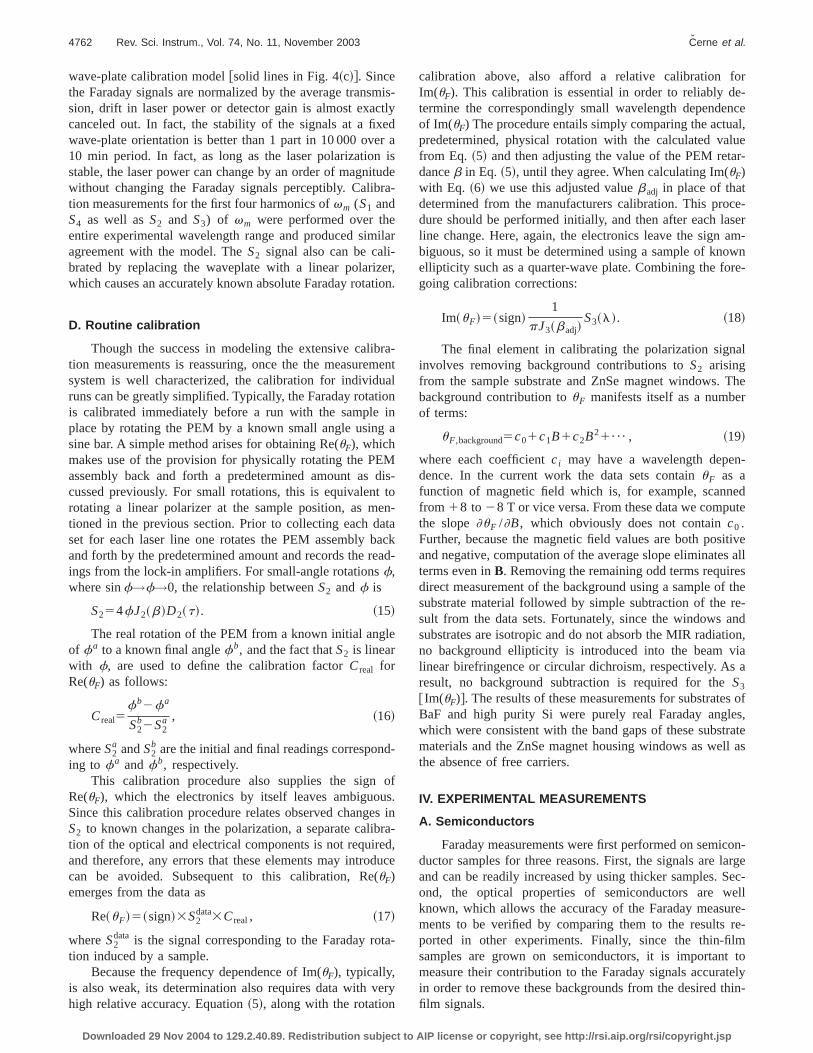
FIG. 5. Re(uF) as a function of frequency squared at 8 T for a GaAs samThe solid line represents av2 fit. The semi-insulating sample is wedgewith an average thickness of 0.42 mm.
Downloaded 29 Nov 2004 to 129.2.40.89. Redistribution subject to AIP
eete
r-py
ani-ndf
d
n
d-h
rofle
ed
3
The second semiconductor material is semi-insulatGaAs. In this case, the frequency dependence of the Farrotation signal is explored. Figure 5 plots Re(uF) as a func-tion of frequency squared at 8 T and 293 K for a Gasample. The solid line represents av2 fit. The semi-insulating sample is wedged with an average thickness0.42 mm. Thev2 frequency behavior of Re(uF) is consistentwith Eq. ~20!. At 8 T and 949 cm21, Re(uF) is approximately331023. The Verdet coefficient is approximately 44°/T mThe value obtained at 10.59mm for Cr-doped15 GaAs byRef. 16 is 41°/T m. This is approximately 50% larger ththat for Si, which is consistent with the fact that GaAs hadirect band gap that is approximately a factor of 2 smathan that of Si. This brings the MIR radiation in GaAs closto the refractive index anisotropy at the band edge. In fathe Re(uF) for GaAs decreased as the temperature is lowewhich is consistent with the increase in the band gap astemperature decreases. As expected, no circular dichrosignal is observed (Im@uF#'0).
The final semiconductor investigated is LaSrGaO4. Thismaterial has the largest band gap, and hence, the smainterband contribution to Re(uF). At 8 T, 293 K, and949 cm21, the Re(uF) is approximately 5.231024 rad for a0.31-mm-thick sample. This translates in a Verdet coefficiat 949 cm21 of 12°/T m. To the authors’ best knowledgthis is the first reported measurement of the MIR Verdetefficient in LaSrGaO4. Despite the onset of strong absortion by phonons for radiation below 1000 cm21, LaSrGaO4
proved to be an excellent substrate due to its weak contrtion to the Re(uF) background. Note that as the frequencydecreased, the strength of the semiconductor Faraday sigdecreases@Eq. ~20!# while the signal from the free carriers ithe thin-film metallic samples increases@Eq. ~20!#. As a re-sult, the lower frequency measurements are simplermore accurate.
B. High temperature superconductorBi2Sr2Ca1Cu2O8¿d
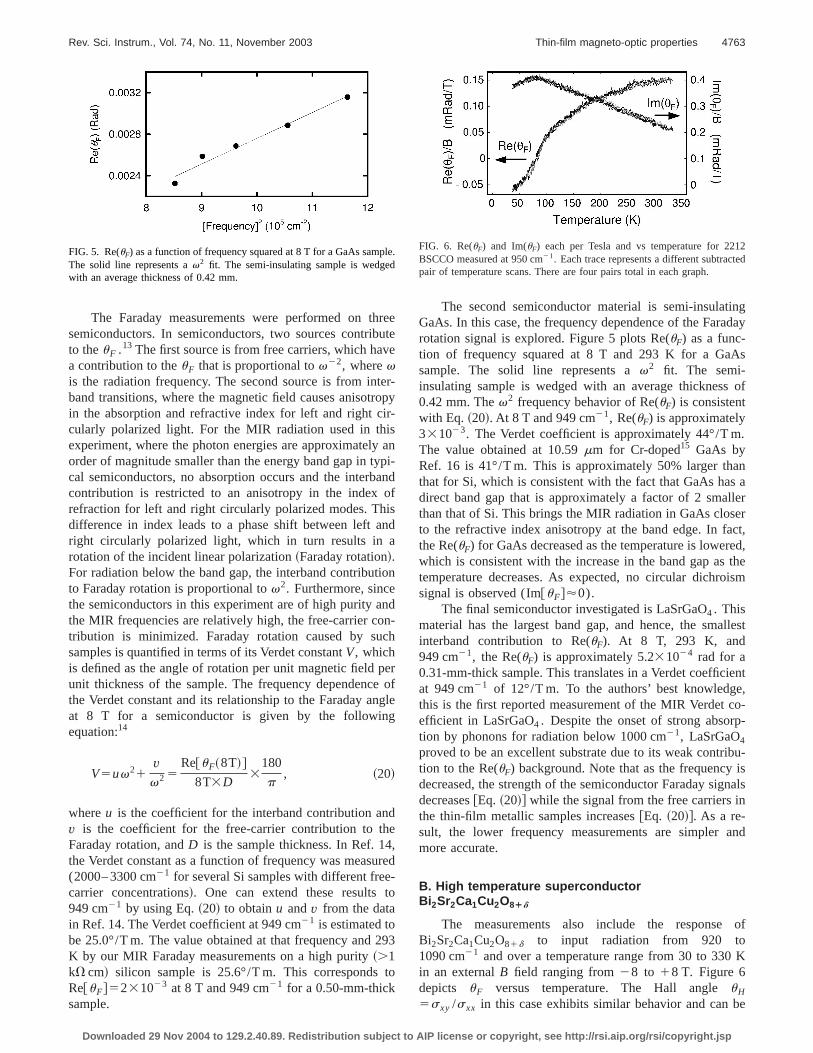
The measurements also include the responseBi2Sr2Ca1Cu2O81d to input radiation from 920 to1090 cm21 and over a temperature range from 30 to 330in an externalB field ranging from28 to 18 T. Figure 6depicts uF versus temperature. The Hall angleuH
5sxy /sxx in this case exhibits similar behavior and can
.FIG. 6. Re(uF) and Im(uF) each per Tesla and vs temperature for 22BSCCO measured at 950 cm21. Each trace represents a different subtracpair of temperature scans. There are four pairs total in each graph.
license or copyright, see http://rsi.aip.org/rsi/copyright.jsp

r
ethr
e
ainefa
deth
los
f
w
lts
lsh
an
al-in-ringbye
andt
lack
ter-de-
of
ally
ffetical
teer-
nor-
c-pen-SC
of
ins,inGu
portact
o-putlar-m-asticputlec-l inle.
esendnesasislly,aw
g-
4764 Rev. Sci. Instrum., Vol. 74, No. 11, November 2003 Cerne et al.
readily obtained fromuF .7,8 In fact, the values obtained fouH in this particular run are within 10% ofuF . To form uH
one would usually dividesxy by the value ofsxx corre-sponding to the same temperature and frequency. But, hwe wish to examine that part of the Hall angle related tofree carriers. Interband transitions which are on the orde1 V contribute essentially nothing tosxy . However, we mustremove their somewhat more substantial contribution tosxx
before taking the ratio. In CGS units
e total5ebound1 i4ps free
v5 i
4ps total
v, ~21!
s free5s total1ivebound
4p. ~22!
As with uF in Fig. 6, Re(uH) increases with temperaturbut appears to saturate around 300 K. Re(uH) is positive forall temperatures in the normal state and does not showstriking discontinuity atTc at 90 K. These data appearRef. 9 where it is compared with far-infrared data from R17. The results show a significant disconnect from the behior of Re(uH) in the existing data for YBa2Cu3O7 in the farinfrared, which indicate a negative value for Re(uF) above250 cm21, whereas that of the current work at 1000 cm21 ispositive. The current work when analyzed using an extenDrude formalism results in a Hall mass comparable toangular-resolved photoemission spectroscopy~ARPES!Fermi mass and a scattering rate comparable to the dcgitudinal, dc Hall, and far-infrared Hall scattering ratewhich, however, are only14 of the ARPES values.
C. Metal films
Figure 7 shows theS2 and S3 signals as a function omagnetic fieldB at room temperature for a Cu thin-filmsample. The MIR radiation frequency is 949 cm21. Thebackground contribution due to the substrate and windohas not been removed. Note the negative offset in theS2
data. The signals are linear inB, as expected.It is interesting to compare the MIR Hall effect resu
on HTSC ~Refs. 8, 9, and 18! with those on Au and Cufilms.2,7 Surprisingly, the Hall angle results for both materiaare qualitatively similar, and are well parametrized by tDrude form foruH . For both systems, the scattering rategH
associated with the Hall angle is linear in temperature
FIG. 7. S2 andS3 normalized signals for a Cu film as a function of manetic field at 949 cm21 and 290 K.
Downloaded 29 Nov 2004 to 129.2.40.89. Redistribution subject to AIP
re,eof
ny
.v-
de
n-,
s
e
d
independent of frequency. In Au and Cu the longitudinscattering rategxx ~obtained from infrared conductivity measurements! is also temperature dependent and frequencydependent as expected from electron–phonon scattewhen the measurement frequency is higher than the Defrequency. For optimally doped YBa2Cu3O7 in the MIR,however, whilegH has a strong temperature dependenceno frequency dependence,gxx is temperature independenbut frequency dependent@as found in infrared conductivity19
and ARPES ~Ref. 20!#. The behavior ofgxx precludesphonons or magnons as the dominant scatterers, and theof frequency dependence ofgH is in contrast to the predictedand observed behavior of a Fermi liquid or inelastic scating in general. Therefore, the frequency and temperaturependence ofgH that are reported in the MIR~Ref. 8! arehighly unusual and indicate a non-Fermi liquid behaviorthe normal state of YBa2Cu3O7. Similar results have beenobtained recently in other HTSC materials such as optimdoped Bi2Sr2CaCu2O8 ~Ref. 9! and underdopedYBa2Cu3O7.18 These results are not yet understood. Ioand Millis21 have recently proposed a model of quasi-elasscattering from superconducting fluctuations in the normstate of highTc materials that leads to a relaxatioon rabehavior similar to that observed. Effects attributed to supconducting fluctuations have also been observed in themal state of underdoped Bi2Sr2CACu2O8 in measurementsof the longitudinal conductivity by THz spectroscopy.22
While no interpretation of these experiments is widely acepted it is clear that the frequency and temperature dedence of the Hall response of the normal state in HTserves as a critical test for any theoretical interpretationthe exotic properties of these materials.
ACKNOWLEDGMENTS
The authors wish to extend their thanks to G. S. JenkJ. R. Simpson, and D. B. Romero for their assistanceperforming the various reported measurements, and G.and J. J. Tu for supplying the BSCCO sample and transdata. This work was supported by the NSF under ContrNo. DMR 0070959
APPENDIX A: POLARIZATION ANALYSIS USINGDIRAC NOTATION
In polarimetric measurements a train of optical compnents, along with a sample, modify or operate on an inbeam, which is in some state of known intensity and poization. Optical components typically include somewhat iperfect devices such as polarizers, wave plates, photoelmodulators, and mechanical rotators. The modified outbeam generally strikes a detector producing an output etrical signal. Here, we develop a general formalism usefurelating the electrical signal to the properties of the sampThe formalism uses Dirac notation, which well differentiatbetween a vector or stateuc& and its representation in sombasis:^xuc&. In polarimetry the usual bases are linear acircular polarizations. The formalism also replaces the Jomatrices with generalized operators and introduces the btransformations and geometrical rotation operations. Finathe result is related to the output of the typical square-loptical detector.
license or copyright, see http://rsi.aip.org/rsi/copyright.jsp

es
r
vedia
tiv
ae
ige
edFb
sf
m-long
eir
h is
for
is
or,
rmaledaryua-
4765Rev. Sci. Instrum., Vol. 74, No. 11, November 2003 Thin-film magneto-optic properties
In what follows, the direction of propagation is in thpositivez direction and all angles are measured in the potive radial direction off thex axis and about thez axis. Be-ginning with the input beam, the formalism simply consideit to be a non-normalized ket
u in&.
Expressed in the linear polarization basis it is
u in&5(L
uL&^Lu in&5ux&^xu in&1uy&^yu in&,
or in the circular basis
u in&5(C
uC&^Cu in&5up&^pu in&1un&^nu in&,
whereup& indicates an electric vector rotating in the positiradial direction about thez axis as seen at a fixed point anun& indicates an electric vector rotating in the negative raddirection about thez axis also as seen at a fixed point.up&and un& are also referred to as having positive and negahelicity. In matrix notation
^Lu in&5S Ex
EyD and ^Cu in&5S Ep
EnD .
The various components in the optical train appearoperators acting on the input ket to produce the output k
uout&5TVW u in&.
In the linear basis this is
uout& 5uL&^LuTVWuL8u in&
5uL&^LuTuL9&^L9uVuL-&^L-uWuL8&^L8u in&
5uL&^LuTuL&^LuVuL&^LuWuL&^Lu in&,
where summation is assumed over repeated state destions L; and the primes have been dropped with the undstanding that the order of the matrices will not be chang
Some devices or operations such as geometric andaday rotations are most easily represented in the circularsis. The transformation matrices,^CuL& and ^LuC&, are themeans of conversion between these two bases. The tranmation for states proceeds as
u in&5(L
uL&^Lu in&
5(LC
uC&^CuL&^Lu in&
5uC&^CuL&^Lu in&,
and for operators as
T5 (L,L8
uL&^LuTuL8&^L8u
5 (L,L8
(C,C8
uC&^CuL&^LuTuL8&^L8uC&^C8u
5uC&^CuL&^LuTuL&^LuC&^Cu.
Downloaded 29 Nov 2004 to 129.2.40.89. Redistribution subject to AIP
i-
s
l
e
st:
na-r-.ar-a-
or-
In matrix representation
^CuL&51
&S 1 2 i
1 i D and ^LuC&51
&S 1 1
i 2 i D .
Below are the representations of some simple optical coponents in the linear bases: a perfect polarizer aligned athe x axis
S 1 0
0 0D ,
a 14 wave plate aligned with slow axis along thex axis
S ei ~p/2! 0
0 1D ,
and a photoelastic modulator aligned along thex axis
S eib cos(2p f t) 0
0 1D .
Another concern for the devices or components is thorientation. Assume, for example, that the operatorT repre-sents the effect of some component such a polarizer whicaligned with its critical direction at an angleu from the xaxis. A simple rotation operation develops an expressionthe rotated polarizer:
T~u!5RTR21,
whereR is an active rotation and in circular representation
^CuR~u!uC&5S e2 iu 0
0 eiuD .
Finally, the output of a square-law type optical detectaside from any responsivity factor, is for our example
d~ t !}^outuout&,
whereuout& is the Hermitian conjugate ofoutu.
APPENDIX B: MULTILAYER RESPONSE USINGRELATIVE IMPEDANCE MATRICES
Assume that some layered materials are arranged noto the z axis and we desire a formalism for the transmittand reflected intensities for plane waves incident at arbitrangles. To begin, the plane wave solution to Maxwell’s eqtions is
Ei ,65Ei ,6eiki ,6•r2 ivt, ~B1!
H i ,65Hi ,6eiki ,6•r2 ivt, ~B2!
where1 represents a wave traveling in the positivez direc-tion at some otherwise arbitrary angle,2 represents a wavetraveling in the negativez direction, andi is the layer num-ber. Then, in CGS:
H i ,65Ae i
m iki ,63Ei ,6 ,
51
Ziki ,63Ei ,6 , CGS, ~B3!
license or copyright, see http://rsi.aip.org/rsi/copyright.jsp
c-
tbe
ry
inin
the
toe-ide
Li,
,
ev.-
n,
and
R.
H.
03.01.
de-ser
4766 Rev. Sci. Instrum., Vol. 74, No. 11, November 2003 Cerne et al.
whereki ,6 is a unit vector parallel to the propagation diretion, e i is the complex dielectric constant of thei th layer andincludes all conductivity effects, andZi5Am i /e i is the rela-tive impedance of the medium, and likee may be complex.
Now that we have a solution inside a layer we needmatch solutions for different layers at the boundariestween layers. The curlE Maxwell equation provides oneboundary condition:
Ei3 z5Ei 113 z. ~B4!
The curl H Maxwell equation provides the other boundacondition:
H i3 z5H i 113 z. ~B5!
To apply the foregoing consider firstS polarization (Eperpendicular to the plane of incidence! at each side of aboundary. In such an instance theE field is tangent to theboundary and if we orient thex andy axes so thatE is alsoperpendicular to they axis, then, from Eq.~B4!:
Ei ,1,x1Ei ,2,x5Ei 11,1,x1Ei 11,2,x . ~B6!
Likewise, substituting Eq.~B3! into Eq. ~B5! produces:
cos~u i
Zi~Ei ,1,x2Ei ,2,x!
5cos~u i 11!
Zi 11~Ei 11,1,x2Ei 11,2,x!, ~B7!
whereu i is the angle of incidence measured of thez axis.Defining the incident impedance forS polarization as
ZS,i5Zi
cos~u i !, ~B8!
Eq. ~B7! becomes
1
ZS,i~Ei ,1,x2Ei ,2,x!
1
5ZS,i 11~Ei 11,1,x2Ei 11,2,x!. ~B9!
Combining Eqs.~B6! and ~B9! into a matrix form:
S Ei 11,1
Ei 11,2D5Si ,i 11S Ei ,1
Ei ,2D , ~B10!
where
Si ,i 1151
2Zs,iS Zs,i1Zs,i 11 Zs,i2Zs,1 i
Zs,i2Zs,i 11 Zs,i1Zs,1 iD . ~B11!
For P polarization~E field i to plane of incidence! definethe incident admittance as
Yp,i51
cos~u i !Zi, ~B12!
then following the same procedure:
Downloaded 29 Nov 2004 to 129.2.40.89. Redistribution subject to AIP
o-
S Hi 11,1
Hi 11,2D5Pi ,i 11S Hi ,1
Hi ,2D , ~B13!
where
Pi ,i 1151
2Yp,iS Yp,i1Yp,i 11 Yp,i2Yp,i 11
Yp,i2Yp,i 11 Yp,i1Yp,i 11D . ~B14!
The E field can be determined fromH using Eq.~B3!.Equations~B8!, ~B10!, and~B11! and Eqs.~B12!, ~B13!,
and ~B14! provide the incident and reflected amplitudesthe i 11 layer at the interface in terms of the amplitudesthe i layer at the interface forS andP polarization, respec-tively. It remains to develop the equations to propagateamplitudes across layeri of thicknessdi . This is alreadyprovided by Eqs.~B1! and ~B2!, which in matrix form be-come
S Ei ,1~z5di !
Ei ,2~z5di !D5S e2 ikW i ,1"zdi 0
0 eikW i ,2"zdiD S Ei ,1~z50!
Ei ,2~z50! D5Ui S Ei ,1~z50!
Ei ,2~z50! D .
So, as an example, given a set of layers numbered 1nfrom left to right, the equation relating the incident and rflected amplitudes on the left side of the set to the right sfor S polarization is
Sn21,nUn21Sn22,n21¯Ui 11Si ,i 11S Ei ,1~ left!Ei ,2~ left! D
5S En,1~right!En,2~right! D .
1J. M. Harris, Y. F. Yan, and N. P. Ong, Phys. Rev. B46, 14293~1992!.2H. D. Drew, S. Wu, and H.-T. S. Lihn, J. Phys.: Condens. Matter8, 10037~1996!.
3H. D. Drew and P. Coleman, Phys. Rev. Lett.78, 1572~1997!.4L. D. Landau, Sov. Phys. JETP3, 920~1957!; 5, 101~1957!; 8, 70 ~1959!.5See, for example, S. G. Kaplan, S. Wu, H.-T. S. Lihn, H. D. Drew, Q.D. B. Fenner, J. M. Phillips, and S. Y. Hou, Phys. Rev. Lett.76, 696~1996!.
6Y. Tokura, A. Urushibara, Y. Moritomo, T. Arima, A. Asamitsu, G. Kidoand N. Furukawa, J. Phys. Soc. Jpn.63, 3931 ~1994!; K. Chahara, T.Ohno, M. Kasai, and Y. Kozono, Appl. Phys. Lett.63, 1990~1993!; R. v.Helmholt, J. Wecker, B. Holzapfel, L. Schultz, and K. Samwer, Phys. RLett. 71, 2331 ~1993!; S. Jin, T. H. Tiefel, M. McCormack, R. A. Fastnacbt, R. Ramesh, and L. H. Chen, Science264, 413~1994!; S. G. Kaplan,M. Quijada, H. D. Drew, D. B. Tanner, G. C. Xiong, R. Ramesh, C. Kwaand T. Venkatesan, Phys. Rev. Lett.77, 2081~1996!.
7J. Cerne, D. C. Schmadel, M. Grayson, G. S. Jenkins, J. R. Simpson,H. D. Drew, Phys. Rev. B61, 8133~2000!.
8J. Cerne, M. Grayson, D. C. Schmadel, G. S. Jenkins, H. D. Drew,Hughes, J. S. Preston, and P. J. Kung, Phys. Rev. Lett.84, 3418~2000!.
9D. C. Schmadel, J. J. Tu, L. B. Rigal, D. B. Romero, M. Grayson, andD. Drew, arXiv:cond-mat/0210304~2002!.
10R. Burdett, Perkin Elmer Instruments, 4/12/00 Application Note No. 1011R. Burdett, Perkin Elmer Instruments, 4/12/00 Application Note No. 1012Several techniques for calibrating the PEM retardance amplitude are
scribed in Appendix A, PEM-90 Photoelastic Modulator Systems UManual from Hinds Instruments~1998!.
13I. G. Mavroides, inOptical Properties of Solids, edited by F. Abele´s~North-Holland, Amsterdam, 1972!.
14G. Ruymbeek, W. Grevendonk, and P. Nagels, Physica B & C89, 14~1977!.
license or copyright, see http://rsi.aip.org/rsi/copyright.jsp

e
g
S.
d .
i,
H.st,
ture
4767Rev. Sci. Instrum., Vol. 74, No. 11, November 2003 Thin-film magneto-optic properties
15Since the free-carrier contribution toV falls of with frequency asv22, we
do not expect this doping to strongly affectV at 1000 cm21. Therefore,
measurements ofV on doped and undoped GaAs should be comparabl
1000 cm21.16C. R. Phipps, S. J. Thomas, and B. Lax, Appl. Phys. Lett.25, 313 ~1974!.17M. Grayson, L. B. Rigal, D. C. Schmadel, H. D. Drew, and P. J. Kun
Phys. Rev. Lett.89, 037003~2002!.18L. B. Rigal, D. C. Schmadel, H. D. Drew, B. Maiorov, E. Osquigil, J.
Preston, R. Hughes, and G. D. Gu, cond-mat/0309108~2003!.
Downloaded 29 Nov 2004 to 129.2.40.89. Redistribution subject to AIP
at
,
19Z. Schlesinger, R. T. Collins, F. Holtzberg, C. Feild, G. Koren, anGupta, Phys. Rev. B41, 11237~1990!.
20T. Valla, A. V. Fedorov, P. D. Johnson, B. O. Wells, S. L. Hulbert, Q. LG. D. Gu, and N. Koshizuka, Science285, 2110~1999!; A. Kaminski, J.Mesot, H. Fretwell, J. C. Campuzano, M. R. Norman, M. Randiera,Ding, T. Sato, T. Takahashi, T. Mochiku, K. Kadowaki, and H. HoechPhys. Rev. Lett.84, 1788~2000!.
21L. B. Ioffe and A. J. Millis, Phys. Rev. B58, 11631~1998!.22J. Corson, R. Mallozzi, J. Orenstein, J. N. Eckstein, and I. Bozovic, Na
~London! 398, 22 ~1999!.
license or copyright, see http://rsi.aip.org/rsi/copyright.jsp