Embed Size (px)
Citation preview
Microanalysis of VLSI Interconnect Failure Modes under Short-Pulse Stress Conditions
Kaustav Banerjee, Dae-Yong Kim, Ajith Amerasekerat, Chenming Hull, S . Simon W o n g and Kenneth E. Goodson
Center for Integrated Systems, Stanford University, Stanford, CA 94305 'ASIC Circuit Design Group, Texas Instruments Inc., Dallas, TX 75243
Department of EECS, University of Califomia, Berkeley, CA, 94720 *I
Tel: (650) 724 2909 E-mail: [email protected]
ABSTRACT
This work presents a detailed microanalysis of interconnect failure mechanisms under short-pulse stress conditions arising during peak current and electrostatic discharge (ESD) events. TEM and SEM analysis have been used to show that passivated AlCu lines can undergo localized melting and voiding under sub-critical current pulses that heat the lines well past their melthg point but below a critical failure temperature causing open circuit failures. It is observed that the damage caused by the melting and voiding remains latent since no physical evidence of damage can be detected under optical microscope and no change in the electrical resistance of these lines can be measured. The voids observed under TEM and SEM result from electromigration under very high current densities and high temperature. TEM diffraction pattems confirm that the molten regions exhibit smaller grain sizes, which are introduced as a result of rapid resolidification from a molten state. A thermo- mechanical model has also been formulated to account for the open circuit failure mode at which the passivation layers are fractured.
INTRODUCTION
Interconnect failure due to short-duration high-current (ESD) stress conditions has become a reliability concem [l-61. Characterization of passivated AlCu lines have been recently reported along with an interconnect heating and failure model under these stress conditions [3, 61. However, there is limited information on the failure mechanisms of these interconnect structures under these stress conditions. Using a transient resistive thermometry technique a critical metal temperature has been shown to be -1000 'C, at which the passivation layer is fractured [3, 61. The interconnect heating characteristics is shown in Figure 1 for the benefit of the readers. It can be observed that the failure temperature is independent of the metal level, or the overlying and underlying dielectric thickness [6]. This motivates the following questions: What causes failures to occur around 1000 'C? How does the dynamics of pulsed lines influence the stress states of the surrounding dielectric? What are the magnitude, direction, and location of the maximum (critical) stress? It is important to understand these issues for advanced interconnect structures in order to optimize their layout and design and to build-in peak-current and ESD reliability into the interconnect design process. Furthermore, latent ESD damage of AlCu interconnects has been reported to be introduced by sub-critical current pulses that does not affect the electrical resistance of the line and shows no physical damage under optical microscope but significantly degrade electromigration (EM) lifetimes [3]. However, no scientific data or evidence has been reported to explain the cause behind this latent damage. A detailed microanalysis of interconnects is therefore desirable to advance the understanding of this failure mode.
4 1200 At = 200 ns
0 2 4 6 a
Current Density, J [xl 0' A/cm2]
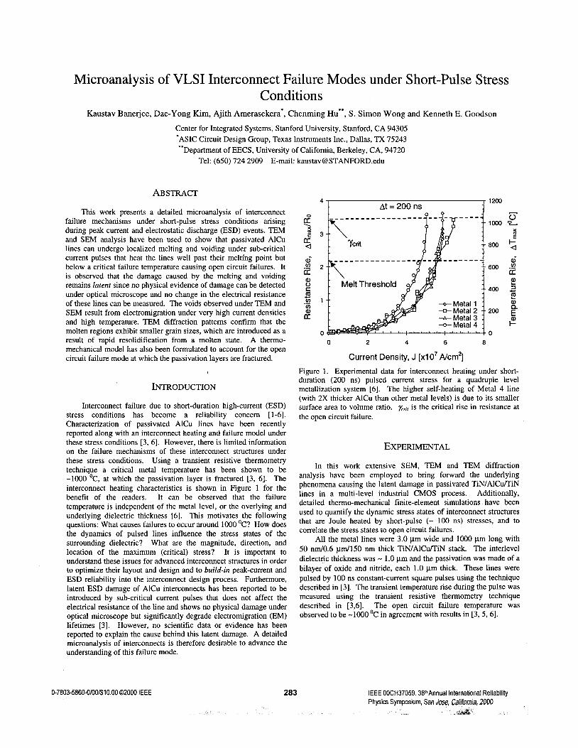
Figure 1. Experimental data for interconnect heating under short- duration (200 ns) pulsed current stress for a quadruple level metallization system [6]. The higher self-heating of Metal 4 line (with 2X thicker AlCu than other metal levels) is due to its smaller surface area to volume ratio. K~~~ is the critical rise in resistance at the open circuit failure.
EXPERIMENTAL
In this work extensive SEM, TEM and TEM diffraction analysis have been employed to bring forward the underlying phenomena causing the latent damage in passivated TiN/AlCu/TiN lines in a multi-level industrial CMOS process. Additionally, detailed thermo-mechanical finite-element simulations have been used to quantify the dynamic stress states of interconnect structures that are Joule heated by short-pulse (- 100 ns) stresses, and to correlate the stress states to open circuit failures.
All the metal lines were 3.0 pm wide and 1000 pm long with 50 nm/0.6 pm/150 nm thick TiN/AlCfl iN stack. The interlevel dielectric thickness was - 1.0 pm and the passivation was made of a bilayer of oxide and nitride, each 1.0 pm thick. These lines were pulsed by 100 ns constant-current square pulses using the technique described in [3]. The transient temperature rise during the pulse was measured using the transient resistive thermometry technique described in [3,6]. The open circuit failure temperature was observed to be -1000 OC in agreement with results in [3,5,6].
0-7803-5860-O/00/$10.00 02000 IEEE 283 IEEE 00CH37059. 38m Annual lntemational Reliability osium, San Jose CaJjbmja, 2000
FAILURE MODES
As mentioned earlier two distinct failure modes were observed in the metal lines pulsed by short-duration high-current pulses:
Latent Failure Mode and Open Circuit Failure Mode
Latent failure mode was observed in metal lines that were pulsed just below the open circuit failure temperature. These lines did not reveal any physical damage or change in resistance. However, in agreement with observations in [3], the mean EM lifetime was reduced by a factor of 4.
We will first present detailed microanalysis of the latent failure mode, provide direct evidence of microstructure change, and then analyze the eventual open circuit failure mechanism.
MICROANALYSIS OF LATENT FAILURE MODES
We first investigated the cause behind the latent damage, which was observed to be introduced by sub-critical current pulses that heat the metal lines past their melting temperature. In order to identify the mechanism responsible for this reliability degradation, detailed microstructure analysis were performed.
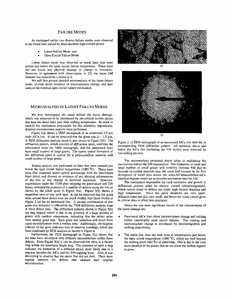
Figure 2(a) shows a TEM micrograph of an unstressed 3.0 pm wide AlCu line. It can be observed that the grain size is - 1.5 pm. A TEM diffraction analysis result is also shown in Figure 2(b). The diffraction pattern, which consists of diffraction spots, confirms the information from the TEM micrograph, that the unstressed lines have small number of large grains. The sparse spatial formation of the diffraction spots is typical for a polycrystalline material with small number of large grains.
Similar analysis was performed on lines that were stressed just below the open circuit failure temperature (1000 OC). These lines were first examined under optical microscope with the passivation layer intact, and showed no evidence of any physical deformations of the line or any change in electrical resistance. However, examination under the TEM after stripping the passivation and TiN layers, revealed the presence of a number of defects along the line as shown by the white spots in Figure 3(a). Figure 3(b) shows a magnified view of one such spot. It can be observed that the grain sizes around these defect sites are much smaller than those shown in Figure 2 (a) for an unstressed line. A second confirmation of this grain size reduction is offered by the TEM diffraction analysis done at these defect sites. The diffraction pattems shown in Figure 5(b) are ring shaped, which is due to the presence of a large number of grains with random orientations, indicating that the defect areas have smaller grain size. Such grain size reduction will result from rapid resolidification from a molten state. Additionally, the brighter contrast of the spots indicates loss of material (voiding), which has been confirmed by SEM analysis as shown in Figure 4.
Furthermore, the E M micrograph in Figure 5(a) shows that the lines have developed very different microstructure within these defects. From Figure 5(b) it can be observed that there is a fainter ring within the innermost bright ring. The presence of such a ring indicates the formation of a different phase, most likely due to a reaction between the AlCu and the TiN-capping layer. Also, it was interesting to observe that the entire line did not melt. There were regions between the defects that retained their original microstructure.
Figure 2. a) TEM micrograph of an unstressed AlCu line with the b) corresponding TEM diffraction pattem. All materials above and below the AlCu line (including the TiN layers) were removed by ion-milling process.
The microanalysis presented above helps in explaining the mechanism behind the EM degradation. The formation of voids and large number of small grains will certainly increase EM due to increase in current densities near the voids and increase in the flux divergence of metal ions across the solid-AlCu/resolidified-AICu interface regions which act as possible nucleation sites for EM.
The mechanism responsible for void nucleation and growth is diffusional process aided by electric current (electromigration), which causes metal to diffuse out under high current densities and high temperature. Since the pulse durations are very small, diffusion times are also very small, and hence the voids cannot grow to critical sizes to affect line resistance.
Hence the two most significant results of the microanalysis of the latent damage are:
Passivated AlCu lines show microstructure change and voiding before catastrophic open circuit failures. The voiding and microstructure change is introduced by electromigration and melting respectively.
The entire line does not melt even at temperatures just below the open circuit temperature (1000 OC), which are well beyond the melting point (660 OC) of aluminum. This is due to the very short duration of the pulses that do not allow the molten regions to grow.
284
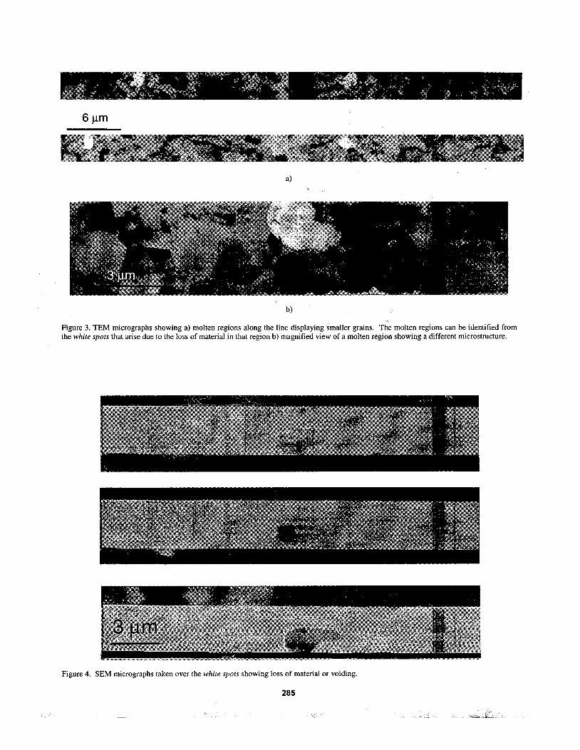
Figure 3. TEM micrographs showing a) molten regions along the line displaying smaller grains. The molten regions can be identified from the while spors that arise due to the loss of material in that region b) magnified view of a molten region showing a different microstructure.
Figure 4. SEM micrographs taken over the white spots showing loss of material or voiding.
285
Metal 1 a)
b) Figure 5. a) Microstructure of the metal within the defects showing small grain sizes b) "EM dcTraction rings validating the presence of a large number of small grains with random orientations. The innermost faint ring (shown by the arrows) indicates the appearance of a new phase.
MICROANALYSIS O F OPEN CIRCUIT FAILURE MODES
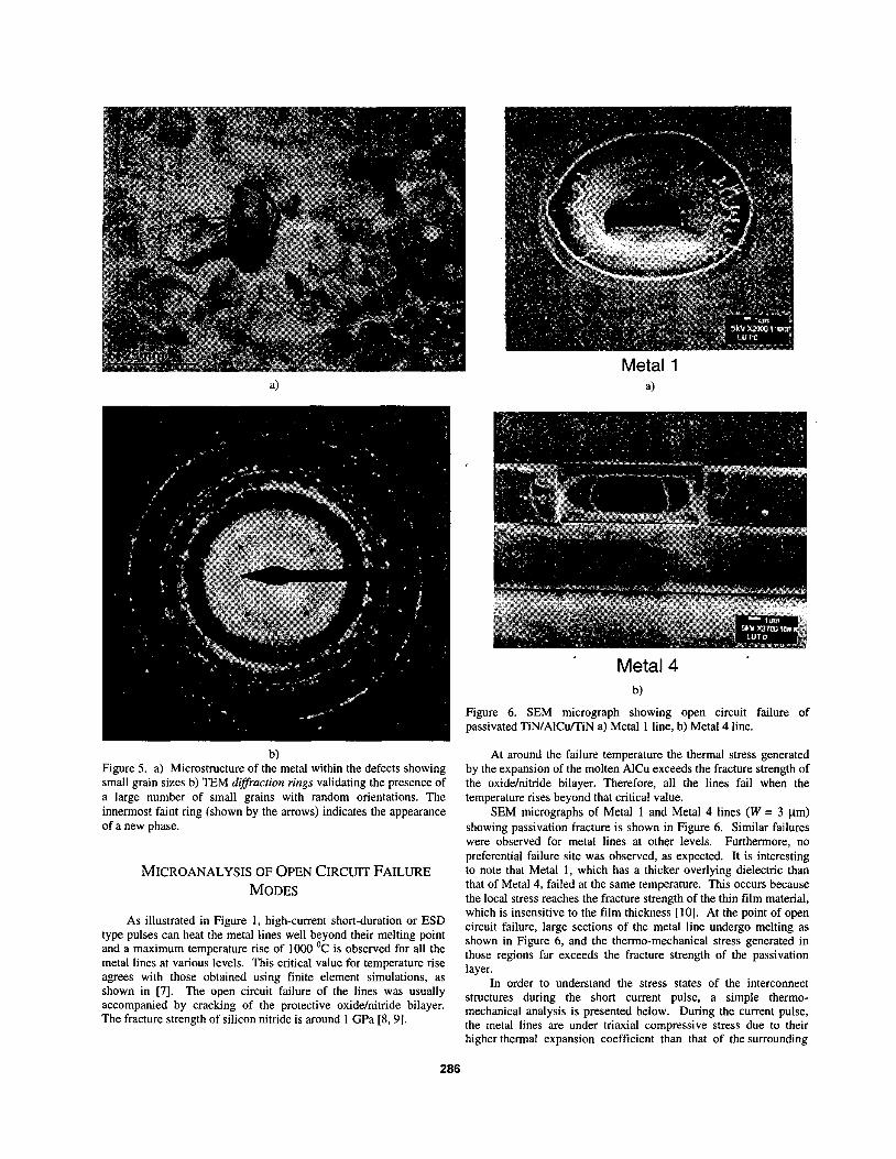
As illustrated in Figure 1, high-current short-duration or ESD type pulses can heat the metal lines well beyond their melting point and a maximum temperature rise of 1000 OC is observed for all the metal lines at various levels. This critical value for temperature rise agrees with those obtained using finite element simulations, as shown in [7]. The open circuit failure of the lines was usually accompanied by cracking of the protective oxidehitride bilayer. The fracture strength of silicon nitride is around 1 GPa [8, 91.
Metal 4 b)
Figure 6. SEM micrograph showing open circuit failure of passivated TiN/AICu/TiN a) Metal 1 line, b) Metal 4 line.
At around the failure temperature the thermal stress generated by the expansion of the molten AlCu exceeds the fracture strength of the oxidehitride bilayer. Therefore, all the lines fail when the temperature rises beyond that critical value.
SEM micrographs of Metal 1 and Metal 4 lines (W = 3 pm) showing passivation fracture is shown in Figure 6. Similar failures were observed for metal lines at other levels. Furthermore, no preferential failure site was observed, as expected. It is interesting to note that Metal 1, which has a thicker overlying dielectric than that of Metal 4, failed at the same temperature. This occurs because the local stress reaches the fracture strength of the thin film material, which is insensitive to the film thickness [lo]. At the point of open circuit failure, large sections of the metal line undergo melting as shown in Figure 6, and the thermo-mechanical stress generated in those regions far exceeds the fracture strength of the passivation layer.
In order to understand the stress states of the interconnect structures during the short current pulse, a simple thermo- mechanical analysis is presented below. During the current pulse, the metal lines are under triaxial compressive stress due to their higher thermal expansion coefficient than that of the surrounding
286
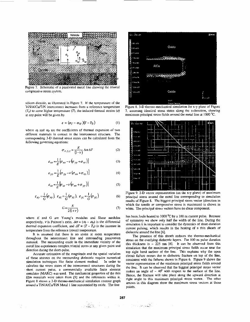
Figure 7. Schematic of a passivated metal line showing the triaxial compressive stress system.
silicon dioxide, as illustrated in Figure 7. If the temperature of the TiN/AlCu/TiN interconnect increases from a reference temperature (To) to some higher temperature (7). the induced thermal strains (E) at any point will be given by
where a, and a// are the coefficients of thermal expansion of two different materials in contact in the interconnect structure. The corresponding 3-D thermal stress states can be calculated from the following governing equations:
E AaAT =x,y,z = - 0-v )
1 Ezz =-h E -v (on +o,)]
E G=- 2(1+v) (7)
where E and G are Young's modulus and Shear modulus respectively, v is Poisson's ratio, A a = (a' - air) is the differential thermal expansion coefficient, and AT = (T - To) is the increase in temperature from the reference (room) temperature.
It is assumed that there is no stress at room temperature throughout the interconnect line and surrounding passivation material. The surrounding oxide in the immediate vicinity of the metal line experiences complex triaxial stress at any given point and direction during the short-pulse.
Accurate estimation of the magnitude and the spatial variation of these stresses on the surrounding dielectric require numerical simulation techniques like finite element method, In order to calculate the stress states of the interconnect structures during the short current pulse, a commercially available finite element simulator (MARC) was used. The mechanical properties of the thin film materials were taken from [9] and the references within it. Figure 8 shows a 3-D thermo-mechanical simulation contour graph around a TiN/AlCu/TiN Metal 1 line surrounded by oxide. The line
7, assuming identical stress states along the z-direction, showing maximum principal stress fields around the metal line at 1000 'C.
F 3gure 9. 2-D vector representation (on the x-y plane) of maximu m principal stress around the metal line corresponding to simulation results of Figure 8. The biggest principal stress vector (direction in which the tensile or compressive stress is maximum) is shown in white. The principal stress vectors have no shear component.
has been Joule heated to 1000 'C by a 100 ns current pulse. Because of symmetry we show only half the width of the line. During the simulation it is important to consider the dynamics of short-duration current pulsing, which results in the heating of a thin sheath of dielectric around the line [6].
The presence of this sheath reduces the thenno-mechanical stress on the overlying dielectric layers. For 100 ns pulse duration this thickness is - 225 nm [6]. It can be observed from this simulation that the maximum principal stress fields occur near the top right hand surface of the line. This explains why the open circuit failure occurs due to dielectric fracture on top of the line, consistent with the failures shown in Figure 6. Figure 9 shows the vector representation of the maximum principal stress fields around the line. It can be observed that the biggest principal stress vector makes an angle of - 40' with respect to the surface of the line. Hence, the fracture will take place along the upward direction at right angle to this maximum principal stress vector. The other arrows in this diagram show the maximum stress vectors at those points.
287
CONCLUSIONS Nitride at 25 ‘C Oxide at 25 C
1 .O pm
m
0 0 200 400 600 800 1000 1200
Metal Temperature, T, [‘Cl
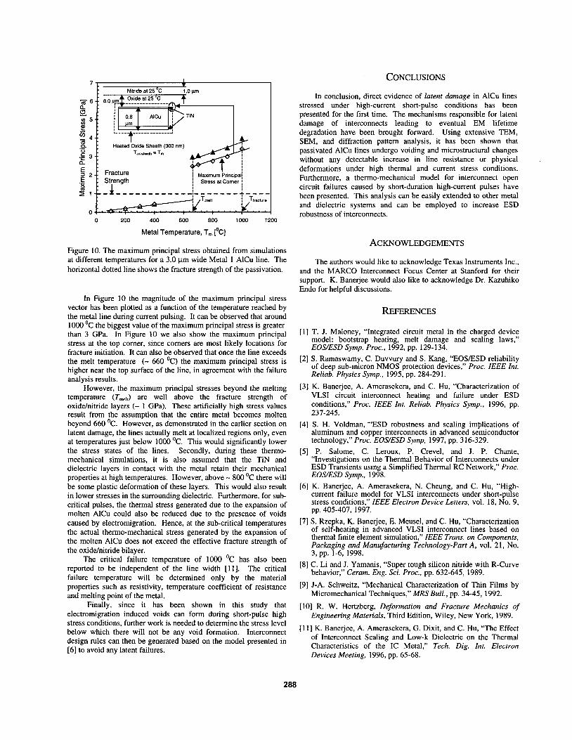
Figure 10. The maximum principal stress obtained from simulations at different temperatures for a 3.0 pm wide Metal 1 AlCu line. The horizontal dotted line shows the fracture strength of the passivation.
In Figure 10 the magnitude of the maximum principal stress vector has been plotted as a function of the temperature reached by the metal line during current pulsing. It can be observed that around lo00 ‘C the biggest value of the maximum principal stress is greater than 3 GPa. In Figure 10 we also show the maximum principal stress at the top comer, since comers are most likely locations for fracture initiation. It can also be observed that once the line exceeds the melt temperature (- 660 ‘C) the maximum principal stress is higher near the top surface of the line, in agreement with the failure analysis results.
However, the maximum principal stresses beyond the melting temperature (T,!,) are well above the fracture strength of oxiddnitride layers (- 1 GPa). These artificially high stress values result from the assumption that the entire metal becomes molten beyond 660 ‘C. However, as demonstrated in the earlier section on latent damage, the lines actually melt at localized regions only, even at temperatures just below 1000 ‘C. This would significantly lower the stress states of the lines. Secondly, during these thermo- mechanical simulations, it is also assumed that the TiN and dielectric layers in contact with the metal retain their mechanical properties at high temperatures. However, above - 800 ‘C there will be some plastic deformation of these layers. This would also result in lower stresses in the surrounding dielectric. Furthermore, for sub- critical pulses, the thermal stress generated due to the expansion of molten AlCu could also be reduced due to the presence of voids caused by electromigration. Hence, at the sub-critical temperatures the actual thermo-mechanical stress generated by the expansion of the molten AlCu does not exceed the effective fracture strength of the oxiddnitride bilayer.
The critical failure temperature of 1000 ‘C has also been reported to be independent of the line width [ l l ] . The critical failure temperature will be determined only by the material properties such as resistivity, temperature coefficient of resistance and melting point of the metal.
Finally, since it has been shown in this study that electromigration induced voids can form during short-pulse high stress conditions, further work is needed to determine the stress level below which there will not be any void formation. Interconnect design rules can then be generated based on the model presented in [6] to avoid any latent failures.
In conclusion, direct evidence of latent damage in AlCu lines stressed under high-current short-pulse conditions has been presented for the first time. The mechanisms responsible for latent damage of interconnects leading to eventual EM lifetime degradation have been brought forward. Using extensive TEM, SEM, and diffraction pattem analysis, it has been shown that passivated AlCu lines undergo voiding and microstructural changes without any detectable increase in line resistance or physical deformations under high thermal and current stress conditions. Furthermore, a thermo-mechanical model for interconnect open circuit failures caused by short-duration high-current pulses have been presented. This analysis can be easily extended to other metal and dielectric systems and can be employed to increase ESD robustness of interconnects.
ACKNOWLEDGEMENTS
The authors would like to acknowledge Texas Instruments Inc., and the MARC0 Interconnect Focus Center at Stanford for their support. K. Banerjee would also like to acknowledge Dr. Kazuhiko Endo for helpful discussions.
REFERENCES
[l ] T. J. Maloney, “Integrated circuit metal in the charged device model: bootstrap heating, melt damage and scaling laws,” EOS/ESD Symp. Proc., 1992, pp. 129- 134.
[2] S. Ramaswamy, C. Duvvury and S. Kang, “EOSESD reliability of deep sub-micron NMOS protection devices,” Proc. IEEE Int. Reliab. Physics Symp., 1995, pp. 284-291.
[3] K. Banerjee, A. Amerasekera, and C. Hu, “Characterization of VLSI circuit interconnect heating and failure under ESD conditions,” Proc. IEEE Int. Reliab. Physics Symp., 1996, pp.
[4] S. H. Voldman, “ESD robustness and scaling implications of aluminum and copper interconnects in advanced semiconductor technology,” Proc. EOYESD Symp, 1997, pp. 3 16-329.
[5] P. Salome, C. Leroux, P. Crevel, and J. P. Chante, “Investigations on the Thermal Behavior of Interconnects under ESD Transients using a Simplified Thermal RC Network,” Proc. EOS/ESD Symp., 1998.
[6] K. Banerjee, A. Amerasekera, N. Cheung, and C. Hu, “High- current failure model for VLSI interconnects under short-pulse stress conditions,” IEEE Electron Device Letters, vol. 18, No. 9,
[7] S. Rzepka, K. Banerjee, E. Meusel, and C. Hu, “Characterization of self-heating in advanced VLSI interconnect lines based on thermal finite element simulation,” IEEE Trans. on Components, Packaging and Manufacturing Technology-Part A, vol. 21, No.
[SI C. Li and J. Yamanis, “Super tough silicon nitride with R-Curve behavior,” Ceram. Eng. Sci. Proc., pp. 632-645, 1989.
[9] J-A. Schweitz, “Mechanical Characterization of Thin Films by Micromechanical Techniques,” MRS Bull., pp. 34-45, 1992.
[lo] R. W. Hertzberg, Deformation and Fracture Mechanics of Engineering Materials, Third Edition, Wiley, New York, 1989.
[ 1 11 K. Banerjee, A. Amerasekera, G. Dixit, and C. Hu, “The Effect of Interconnect Scaling and Low-k Dielectric on the Thermal Characteristics of the IC Metal,” Tech. Dig. Int. Electron Devices Meeting, 1996, pp. 65-68.
23 7- 245.
pp. 405-407, 1997.
3, pp. 1-6, 1998.
288