Embed Size (px)
Citation preview
Research ArticleMicrocontroller Based Flexible ModulationScheme of MLI Operation for Selective Lower Levels:A Knowledge Based Approach
R. K. Dhatrak,1 R. K. Nema,1 and D. M. Deshpande2
1Department of Electrical Engineering, Maulana Azad National Institute of Technology, Bhopal 462051, India2Department of Electrical and Electronics Engineering, Sagar Institute of Research Technology and Science, Bhopal 462051, India
Correspondence should be addressed to R. K. Dhatrak; [email protected]
Received 30 November 2015; Revised 7 April 2016; Accepted 13 April 2016
Academic Editor: Jiun-Wei Horng
Copyright © 2016 R. K. Dhatrak et al. This is an open access article distributed under the Creative Commons Attribution License,which permits unrestricted use, distribution, and reproduction in any medium, provided the original work is properly cited.
In today’s industrial world multilevel inverter (MLI) got a significant importance in medium voltage application and also a verypotential topic for researchers. It is experienced that studying and comparing results of multilevel inverter (MLI) at distinct levelsare a costlier and time consuming issue for any researcher if he fabricate different inverters for each level, as designing powermodules simultaneously for different level is a cumbersome task. In this paper a flexible quotient has been proposed to recognizepossible conversion of availableMLI to few lower level inverters by appropriately changingmicrocontroller programming.This is anattempt to obtain such change in levels through simulation using MATLAB Simulink on inductive load which may also be appliedto induction motor. Experimental results of pulse generation using dsPIC33EP256MC202 demonstrate the feasibility of proposedscheme. Proposed flexible quotient successfully demonstrates that a five-level inverter may be operated as three and two levels also.The paper focuses on odd levels only as common mode voltage (CMV) can be reduced to zero and performance of drives is betterthan even level. Simulated and experimental results are given in paper.
1. Introduction
It is a laborious and costlier work to design different levelinvertermodules to investigate any particular issue. To obtaindifferent level operations from a single power module is abetter solution to this issue. In this paper an attempt has beendone to address this issue. This method makes it possible todesign at least three different level inverters from any higher(more than five) odd level inverter. Two- and three-levelinverter can be designed from any odd level inverter havinglevels more than five by properly programming microcon-troller. A flexible quotient proposed will help researchers toforecast possible inverter operations at few lower levels usingthe available higher MLI.
A five-level inverter can be used as two- as well asfive-level inverter using sinusoidal pulse width modula-tion (SPWM) and space vector pulse width modulation(SVPWM) technique [1, 2]. It is possible to design a controller
programming for SVPWM and SPWM. In this paper SPWMtechnique has been implemented. The same scheme can beextended to cascade H-bridge and flying capacitor MLI, byproperly selecting the switching states of inverter. As thenumber of switches used in these basic topologies is same,for predicting the possible conversion ofMLI same techniquemay be used but modulation scheme is different for differenttopologies. Modulation scheme in H-bridge is quiet similarto diode clamped inverter but in flying capacitor it has to beproperly modified.
Investigation on total harmonic distortion (THD) inline voltage, phase voltage, and line current as well asCMV has been done. As the level of inverter increasespercentage THD and CMV also reduce without using extracircuitry like filters. Application of such flexible inverter leveladjustment using available inverter in generalized manner isnot reported in literature. DSP 2812 is used to develop thepulses in the available literature. Instead of using a costlier
Hindawi Publishing CorporationJournal of EngineeringVolume 2016, Article ID 9206124, 11 pageshttp://dx.doi.org/10.1155/2016/9206124
2 Journal of Engineering
0.005 0.010 0.020.015Time (sec)
−2
−1
0
1
2
Am
plitu
de
(a)
0.015 0.020.005 0.010Time (sec)
−2
−1
0
1
2
Am
plitu
de
(b)
0.005 0.010 0.020.015Time (sec)
−2
−1
0
1
2
Am
plitu
de
(c)
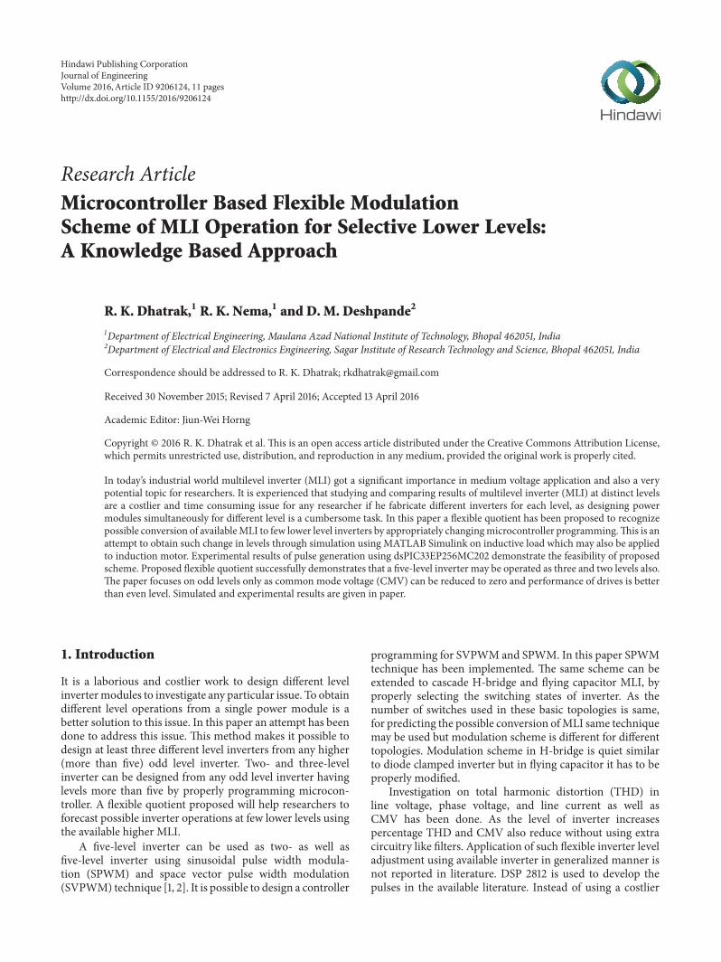
Figure 1: Carrier wave and modulating waveform: (a) PD, (b) POD, and (c) APOD.
and complicated DSP controller a very cheap and simpleprogramming dsPIC33EP256MC202 microcontroller is usedto develop pulses of five-level inverter in this work.
This paper is organized as follows. Basic modulationtechniques are reviewed in Section 2. Importance of diodeclamped multilevel inverter for industrial application is dis-cussed in Section 3. Section 4 gives the basic theme to explainthe principle of this scheme.The development of modulationscheme is discussed in Section 5. Some experimental results,necessary microcontroller circuit, and proper voltage regu-lation circuit for microcontroller are explained in Section 6.Simulation results and their comparisons are discussed inSection 7. Some conclusions are drawn in Section 8.
2. Modulation Techniques
The main modulation techniques used for multilevel invert-ers are summarized as follows [3, 4]:
(1) Sinusoidal pulse width modulation (SPWM).(2) Space vector pulse width modulation (SVPWM).(3) Selective harmonic elimination pulse width modula-
tion (SHEPWM).
First technique can be easily applicable to multilevelinverter by digital controller as it does not require any
complex computation. Second and third techniques arecomplicated as they need some extra computations [3, 4]. Inthis paper focus is on the first method.The number of carriersignals required for 𝑁 level inverter is (𝑁 − 1). Frequencyand peak to peak amplitude of all carrier waves should bethe same. SPWM can be again classified according to thephase position of the triangular carrier waveforms [1, 3, 4] asfollows:
(1) Phase disposition (PD): all carriers are in phase withone another (Figure 1(a)).
(2) Phase opposite disposition (POD): carriers abovezero reference are in phase but in antiphase to thosebelow zero reference (Figure 1(b)).
(3) Alternate phase opposite disposition (APOD): as thename indicates carriers in alternate layers are in phaseopposition (Figure 1(c)).
Above three techniques can be applied with new mod-ulation scheme. Simulation results using PD technique areprovided to validate the scheme. This scheme may also beused with SVPWM and SHEPWMmodulation technique.
3. Multilevel Inverter
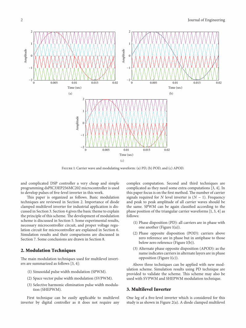
One leg of a five-level inverter which is considered for thisstudy is as shown in Figure 2(a). A diode clamped multilevel
Journal of Engineering 3
G
Vdc4
Vdc4
Vdc4
Vdc4
−+
−+
−+
−+
Sa1
Sa2
Sa3
Sa4
Sa5
Sa6
Sa7
Sa8
(a) Five-level inverter
G
Vdc4 −
+
−+
−+
−+
Vdc4
Vdc4
Vdc4
Vdc4
Sa1
Sa2
Sa3
Sa4
Sa5
Sa6
Sa7
Sa8
(b) Three-level inverter
G
Vdc4
Vdc4
Vdc4
Vdc4
Vdc4
−+
−+
−+
−+
Sa1
Sa2
Sa3
Sa4
Sa5
Sa6
Sa7
Sa8
(c) Two-level inverter
Figure 2: Various inverter configurations.
inverter topology has been used since it requires only one dcsource and can be easily used formediumvoltage applicationsin industries. One of the serious issues of diode clampedmultilevel inverter is dc-bus voltage unbalancing [5]. Sincevoltage balancing is not concernedwith this study, separate dcsources have been considered for dc buses.The same invertermay function as three-level inverter (Figure 2(b)) and two-level inverter (Figure 2(c)) by changing the gating signals ofthe switches.
4. Methodology
At first one has to decide the maximum level up to whichstudy has to be carried out. Then we may find how manydifferent levelsmay be possible to obtain from the samepowermodule.The total number of switches used in𝑁 level inverterin one limb of the polyphase circuit is 2 ∗ (𝑁 − 1). If seriesconnected switches are used then they should be equallydivided in (𝑁 − 1) groups and each group of switches isturned on simultaneously by controlling circuit. Suppose that𝑁 level inverter has to be converted into two-level inverter;then 2 ∗ (𝑁 − 1)/2 switches are turned on simultaneously.If the same inverter is used for three-level inverter then thetotal number of switches which turned on simultaneouslyis 2 ∗ (𝑁 − 1)/4. In general if 𝑀 is the level to which theavailable𝑁 level inverter is to be converted then the numberof switches required to be turned on simultaneously is 2∗(𝑁−1)/2∗(𝑀−1), that is, (𝑁−1)/(𝑀−1), where𝑀 ≤ 𝑁.The ratio
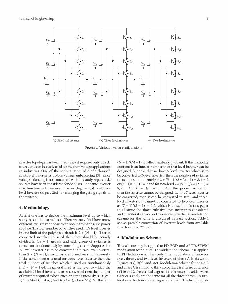
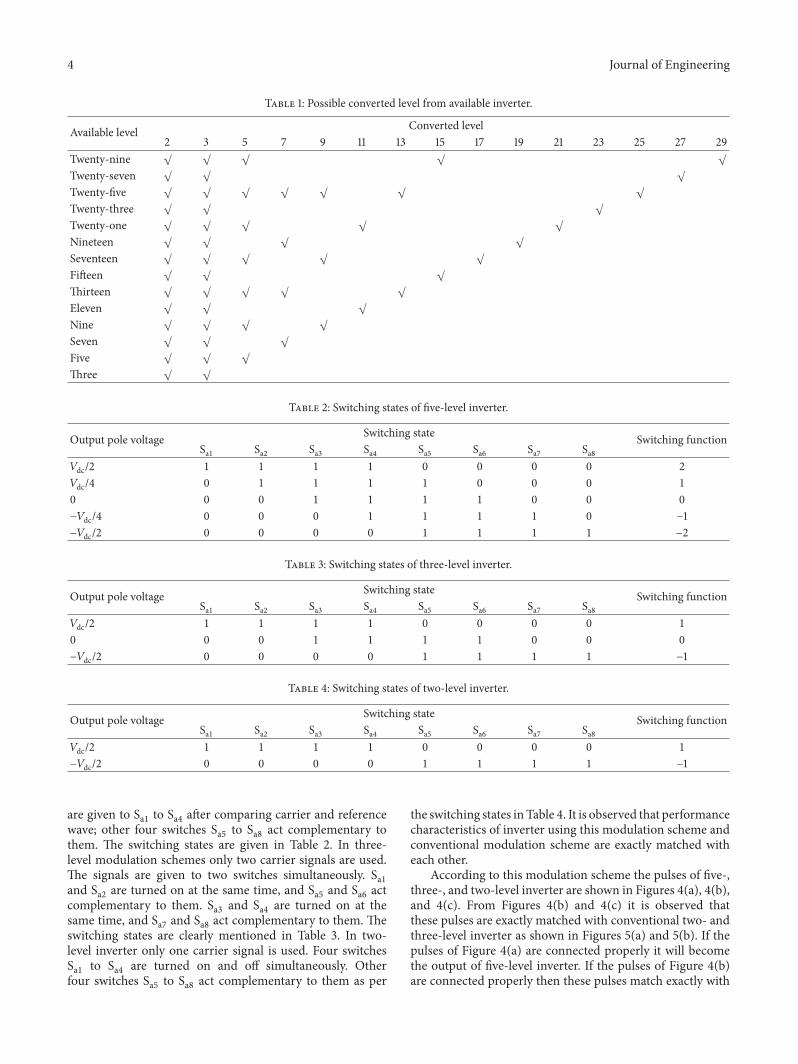
(𝑁 − 1)/(𝑀− 1) is called flexibility quotient. If this flexibilityquotient is an integer number then that level inverter can bedesigned. Suppose that we have 5-level inverter which is tobe converted to 3-level inverter; then the number of switchesturned on simultaneously is 2 ∗ (5 − 1)/2 ∗ (3 − 1) = 8/4 = 2or (5−1)/(3−1) = 2 and for two-level 2∗(5−1)/2∗(2−1) =8/2 = 4 or (5 − 1)/(2 − 1) = 4. If the quotient is fractionthen the inverter cannot be designed. Let the 7-level inverterbe converted; then it can be converted to two- and three-level inverter but cannot be converted to five-level inverteras (7 − 1)/(5 − 1) = 1.5, which is a fraction. In this paperto illustrate the above rule five-level inverter is consideredand operates it as two- and three-level inverter. Amodulationscheme for the same is discussed in next section. Table 1shows possible conversion of inverter levels from availableinverters up to 29 level.
5. Modulation Scheme
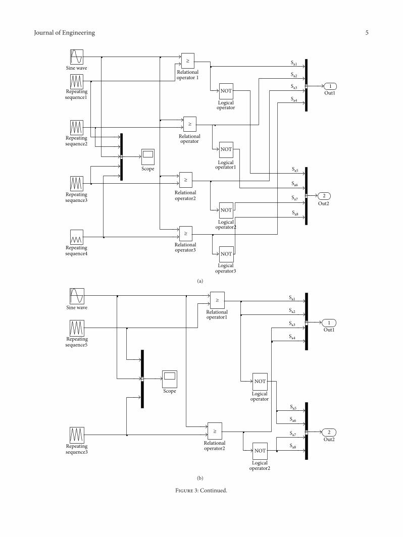
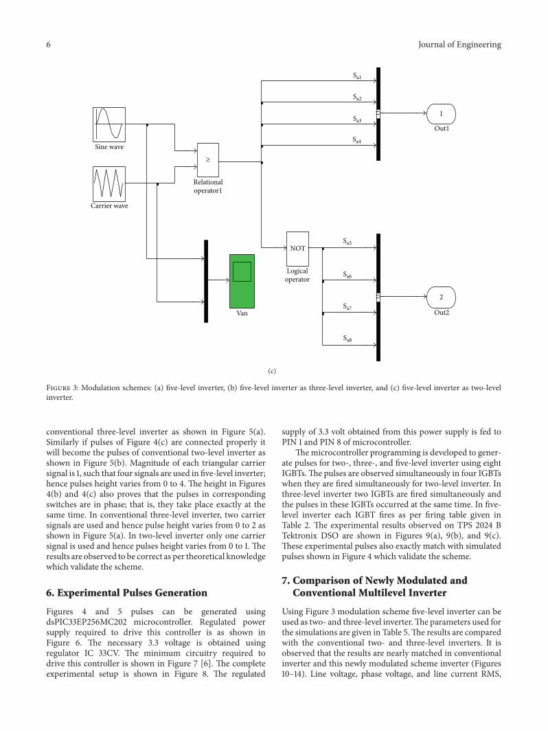
This schememay be applied to PD, POD, and APOD, SPWMmodulation techniques. To validate the scheme it is appliedto PD technique in this study. The modulation scheme forfive-, three-, and two-level inverters of phase A is shown inFigures 3(a), 3(b), and 3(c). Modulation scheme for phase Band phase C is similar to this except there is a phase differenceof 120 and 240 electrical degrees in reference sinusoidal wave.Carrier signals are the same for all the three phases. In five-level inverter four carrier signals are used. The firing signals
4 Journal of Engineering
Table 1: Possible converted level from available inverter.
Available level Converted level2 3 5 7 9 11 13 15 17 19 21 23 25 27 29
Twenty-nine √ √ √ √ √
Twenty-seven √ √ √
Twenty-five √ √ √ √ √ √ √
Twenty-three √ √ √
Twenty-one √ √ √ √ √
Nineteen √ √ √ √
Seventeen √ √ √ √ √
Fifteen √ √ √
Thirteen √ √ √ √ √
Eleven √ √ √
Nine √ √ √ √
Seven √ √ √
Five √ √ √
Three √ √
Table 2: Switching states of five-level inverter.
Output pole voltage Switching state Switching functionSa1 Sa2 Sa3 Sa4 Sa5 Sa6 Sa7 Sa8
𝑉dc/2 1 1 1 1 0 0 0 0 2𝑉dc/4 0 1 1 1 1 0 0 0 10 0 0 1 1 1 1 0 0 0−𝑉dc/4 0 0 0 1 1 1 1 0 −1−𝑉dc/2 0 0 0 0 1 1 1 1 −2
Table 3: Switching states of three-level inverter.
Output pole voltage Switching state Switching functionSa1 Sa2 Sa3 Sa4 Sa5 Sa6 Sa7 Sa8
𝑉dc/2 1 1 1 1 0 0 0 0 10 0 0 1 1 1 1 0 0 0−𝑉dc/2 0 0 0 0 1 1 1 1 −1
Table 4: Switching states of two-level inverter.
Output pole voltage Switching state Switching functionSa1 Sa2 Sa3 Sa4 Sa5 Sa6 Sa7 Sa8
𝑉dc/2 1 1 1 1 0 0 0 0 1−𝑉dc/2 0 0 0 0 1 1 1 1 −1
are given to Sa1 to Sa4 after comparing carrier and referencewave; other four switches Sa5 to Sa8 act complementary tothem. The switching states are given in Table 2. In three-level modulation schemes only two carrier signals are used.The signals are given to two switches simultaneously. Sa1and Sa2 are turned on at the same time, and Sa5 and Sa6 actcomplementary to them. Sa3 and Sa4 are turned on at thesame time, and Sa7 and Sa8 act complementary to them. Theswitching states are clearly mentioned in Table 3. In two-level inverter only one carrier signal is used. Four switchesSa1 to Sa4 are turned on and off simultaneously. Otherfour switches Sa5 to Sa8 act complementary to them as per
the switching states inTable 4. It is observed that performancecharacteristics of inverter using this modulation scheme andconventional modulation scheme are exactly matched witheach other.
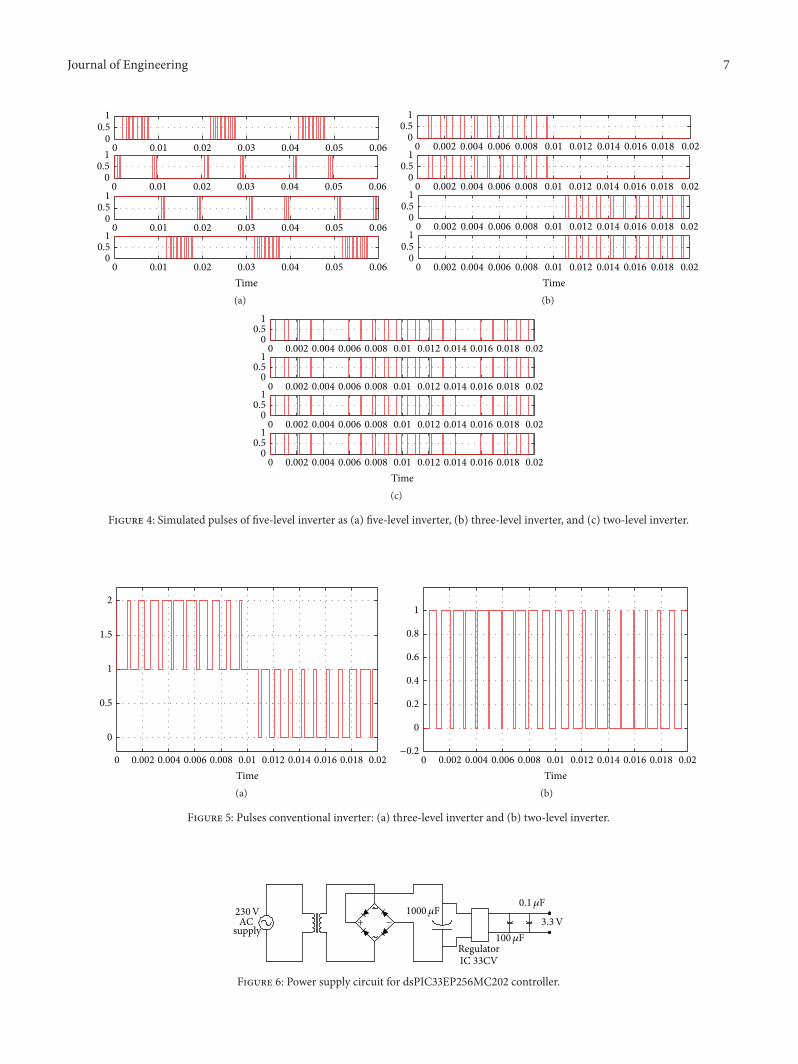
According to this modulation scheme the pulses of five-,three-, and two-level inverter are shown in Figures 4(a), 4(b),and 4(c). From Figures 4(b) and 4(c) it is observed thatthese pulses are exactly matched with conventional two- andthree-level inverter as shown in Figures 5(a) and 5(b). If thepulses of Figure 4(a) are connected properly it will becomethe output of five-level inverter. If the pulses of Figure 4(b)are connected properly then these pulses match exactly with
Journal of Engineering 5
2Out2
1Out1
Sine wave
Scope
Repeatingsequence2
Repeatingsequence1
Repeatingsequence3
Repeatingsequence4
Relationaloperator3
Relationaloperator2
Relationaloperator 1
Relationaloperator
NOT
Logicaloperator3
NOT
Logicaloperator2
NOT
Logicaloperator1
NOT
Logicaloperator
Sa8
≥
≥
≥
≥
Sa1
Sa2
Sa3
Sa4
Sa5
Sa6
Sa7
(a)
Repeatingsequence3
Repeatingsequence5
Logicaloperator
2Out2
1Out1
Sine wave
Scope
Relationaloperator2
Relationaloperator1
NOT
Logicaloperator2
NOT
≥
≥
Sa1
Sa2
Sa3
Sa4
Sa5
Sa6
Sa7
Sa8
(b)
Figure 3: Continued.
6 Journal of Engineering
2
Out2
1
Out1
Van
Sine wave
Relationaloperator1
NOT
Logicaloperator
Carrier wave
≥
Sa8
Sa1
Sa2
Sa3
Sa4
Sa5
Sa6
Sa7
(c)
Figure 3: Modulation schemes: (a) five-level inverter, (b) five-level inverter as three-level inverter, and (c) five-level inverter as two-levelinverter.
conventional three-level inverter as shown in Figure 5(a).Similarly if pulses of Figure 4(c) are connected properly itwill become the pulses of conventional two-level inverter asshown in Figure 5(b). Magnitude of each triangular carriersignal is 1, such that four signals are used in five-level inverter;hence pulses height varies from 0 to 4. The height in Figures4(b) and 4(c) also proves that the pulses in correspondingswitches are in phase; that is, they take place exactly at thesame time. In conventional three-level inverter, two carriersignals are used and hence pulse height varies from 0 to 2 asshown in Figure 5(a). In two-level inverter only one carriersignal is used and hence pulses height varies from 0 to 1. Theresults are observed to be correct as per theoretical knowledgewhich validate the scheme.
6. Experimental Pulses Generation
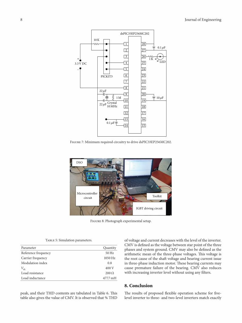
Figures 4 and 5 pulses can be generated usingdsPIC33EP256MC202 microcontroller. Regulated powersupply required to drive this controller is as shown inFigure 6. The necessary 3.3 voltage is obtained usingregulator IC 33CV. The minimum circuitry required todrive this controller is shown in Figure 7 [6]. The completeexperimental setup is shown in Figure 8. The regulated
supply of 3.3 volt obtained from this power supply is fed toPIN 1 and PIN 8 of microcontroller.
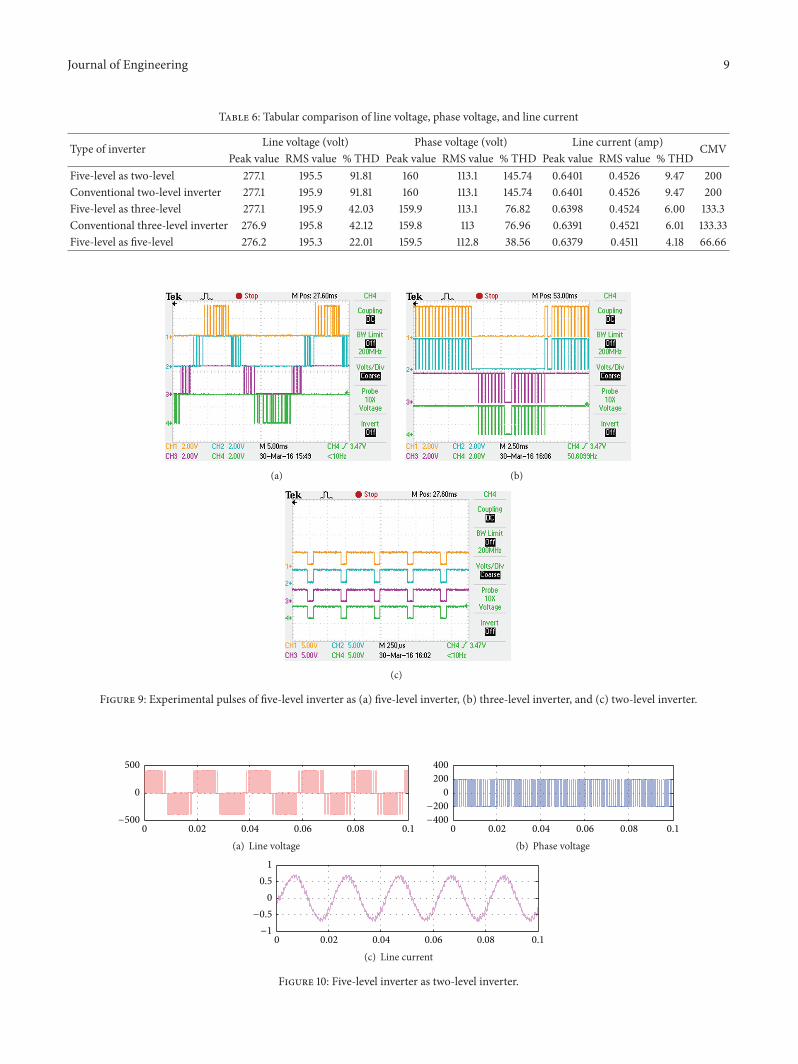
Themicrocontroller programming is developed to gener-ate pulses for two-, three-, and five-level inverter using eightIGBTs.The pulses are observed simultaneously in four IGBTswhen they are fired simultaneously for two-level inverter. Inthree-level inverter two IGBTs are fired simultaneously andthe pulses in these IGBTs occurred at the same time. In five-level inverter each IGBT fires as per firing table given inTable 2. The experimental results observed on TPS 2024 BTektronix DSO are shown in Figures 9(a), 9(b), and 9(c).These experimental pulses also exactly match with simulatedpulses shown in Figure 4 which validate the scheme.
7. Comparison of Newly Modulated andConventional Multilevel Inverter
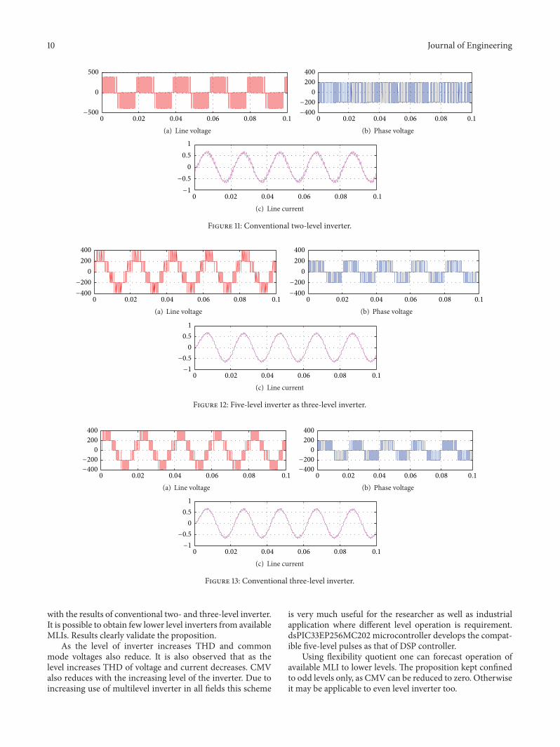
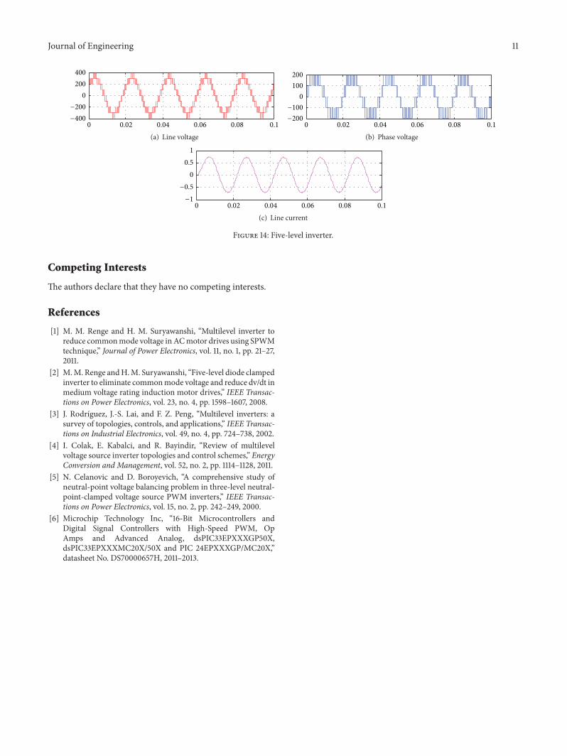
Using Figure 3 modulation scheme five-level inverter can beused as two- and three-level inverter.The parameters used forthe simulations are given in Table 5.The results are comparedwith the conventional two- and three-level inverters. It isobserved that the results are nearly matched in conventionalinverter and this newly modulated scheme inverter (Figures10–14). Line voltage, phase voltage, and line current RMS,
Journal of Engineering 7
0.01 0.02 0.03 0.04 0.05 0.0600
0.51
0.01 0.02 0.03 0.04 0.05 0.0600
0.51
0.01 0.02 0.03 0.04 0.05 0.0600
0.51
00.5
1
0.01 0.02 0.03 0.04 0.05 0.060Time(a)
0.002 0.004 0.006 0.008 0.01 0.0120 0.016 0.018 0.020.0140
0.51
0.002 0.004 0.006 0.008 0.01 0.012 0.014 0.016 0.018 0.0200
0.51
0.002 0.004 0.006 0.008 0.01 0.012 0.014 0.016 0.018 0.0200
0.51
0.002 0.004 0.006 0.008 0.010 0.014 0.016 0.018 0.020.012Time
00.5
1
(b)
0.002 0.004 0.006 0.008 0.01 0.012 0.014 0.016 0.018 0.020
0.002 0.004 0.006 0.008 0.01 0.012 0.014 0.016 0.018 0.020
0.002 0.004 0.006 0.008 0.01 0.012 0.014 0.016 0.018 0.020
00.5
1
00.5
1
00.5
1
00.5
1
0.002 0.004 0.006 0.008 0.01 0.012 0.014 0.016 0.018 0.020Time(c)
Figure 4: Simulated pulses of five-level inverter as (a) five-level inverter, (b) three-level inverter, and (c) two-level inverter.
0.002 0.004 0.006 0.008 0.01 0.012 0.014 0.016 0.018 0.020Time
0
0.5
1
1.5
2
(a)
0.002 0.004 0.006 0.008 0.01 0.012 0.014 0.016 0.018 0.020Time
−0.2
0
0.2
0.4
0.6
0.8
1
(b)
Figure 5: Pulses conventional inverter: (a) three-level inverter and (b) two-level inverter.
ACsupply
RegulatorIC 33CV
230V 1000 𝜇F
100𝜇F3.3V
0.1 𝜇F
−+
Figure 6: Power supply circuit for dsPIC33EP256MC202 controller.
8 Journal of Engineering
dsPIC33EP256MC202
LED
Crystal
PICKIT3
1
2
3
4
6
7
8
9
10
11
12
13
14 15
16
17
18
19
20
21
22
23
25
26
27
28
5 24
0.1 𝜇F
22𝜇F
22𝜇F
10𝜇F
3.3V DC
0.1 𝜇F
−
+
10MHz
1K
10K
1M
Figure 7: Minimum required circuitry to drive dsPIC33EP256MC202.
DSO
ToolkitMicrocontroller
circuit
IGBT driving circuit
Figure 8: Photograph experimental setup.
Table 5: Simulation parameters.
Parameter QuantityReference frequency 50HzCarrier frequency 1050HzModulation index 0.8𝑉dc 400VLoad resistance 200ΩLoad inductance 477.7mH
peak, and their THD contents are tabulated in Table 6. Thistable also gives the value of CMV. It is observed that % THD
of voltage and current decreases with the level of the inverter.CMV is defined as the voltage between star point of the threephases and system ground. CMV may also be defined as thearithmetic mean of the three-phase voltages. This voltage isthe root cause of the shaft voltage and bearing current issuein three-phase induction motor. These bearing currents maycause premature failure of the bearing. CMV also reduceswith increasing inverter level without using any filters.
8. Conclusion
The results of proposed flexible operation scheme for five-level inverter to three- and two-level inverters match exactly
Journal of Engineering 9
Table 6: Tabular comparison of line voltage, phase voltage, and line current
Type of inverter Line voltage (volt) Phase voltage (volt) Line current (amp) CMVPeak value RMS value % THD Peak value RMS value % THD Peak value RMS value % THD
Five-level as two-level 277.1 195.5 91.81 160 113.1 145.74 0.6401 0.4526 9.47 200Conventional two-level inverter 277.1 195.9 91.81 160 113.1 145.74 0.6401 0.4526 9.47 200Five-level as three-level 277.1 195.9 42.03 159.9 113.1 76.82 0.6398 0.4524 6.00 133.3Conventional three-level inverter 276.9 195.8 42.12 159.8 113 76.96 0.6391 0.4521 6.01 133.33Five-level as five-level 276.2 195.3 22.01 159.5 112.8 38.56 0.6379 0.4511 4.18 66.66
(a) (b)
(c)
Figure 9: Experimental pulses of five-level inverter as (a) five-level inverter, (b) three-level inverter, and (c) two-level inverter.
0.02 0.04 0.06 0.08 0.10−500
0
500
(a) Line voltage0.02 0.04 0.06 0.08 0.10
−400
−200
0200400
(b) Phase voltage
−1
−0.5
00.5
1
0.02 0.04 0.06 0.08 0.10(c) Line current
Figure 10: Five-level inverter as two-level inverter.
10 Journal of Engineering
0.02 0.04 0.06 0.08 0.10−500
0
500
(a) Line voltage0.02 0.04 0.06 0.08 0.10
−400
−200
0200400
(b) Phase voltage
−1
−0.5
00.5
1
0.02 0.04 0.06 0.08 0.10(c) Line current
Figure 11: Conventional two-level inverter.
0.02 0.04 0.06 0.08 0.10−400
−200
0200400
(a) Line voltage0.02 0.04 0.06 0.08 0.10
−400
−200
0200400
(b) Phase voltage
0.02 0.04 0.060 0.10.08−1
−0.5
00.5
1
(c) Line current
Figure 12: Five-level inverter as three-level inverter.
0.02 0.04 0.06 0.08 0.10−400
−200
0200400
(a) Line voltage0.02 0.04 0.06 0.08 0.10
−400
−200
0200400
(b) Phase voltage
0.020 0.06 0.08 0.10.04−1
−0.5
00.5
1
(c) Line current
Figure 13: Conventional three-level inverter.
with the results of conventional two- and three-level inverter.It is possible to obtain few lower level inverters from availableMLIs. Results clearly validate the proposition.
As the level of inverter increases THD and commonmode voltages also reduce. It is also observed that as thelevel increases THD of voltage and current decreases. CMValso reduces with the increasing level of the inverter. Due toincreasing use of multilevel inverter in all fields this scheme
is very much useful for the researcher as well as industrialapplication where different level operation is requirement.dsPIC33EP256MC202 microcontroller develops the compat-ible five-level pulses as that of DSP controller.
Using flexibility quotient one can forecast operation ofavailable MLI to lower levels. The proposition kept confinedto odd levels only, as CMV can be reduced to zero. Otherwiseit may be applicable to even level inverter too.
Journal of Engineering 11
0 0.040.02 0.08 0.10.06−400
−200
0200400
(a) Line voltage0.02 0.040 0.08 0.10.06
−200
−100
0100200
(b) Phase voltage
0.02 0.040 0.08 0.10.06−1
−0.5
00.5
1
(c) Line current
Figure 14: Five-level inverter.
Competing Interests
The authors declare that they have no competing interests.
References
[1] M. M. Renge and H. M. Suryawanshi, “Multilevel inverter toreduce commonmode voltage inACmotor drives using SPWMtechnique,” Journal of Power Electronics, vol. 11, no. 1, pp. 21–27,2011.
[2] M.M. Renge andH.M. Suryawanshi, “Five-level diode clampedinverter to eliminate commonmode voltage and reduce dv/dt inmedium voltage rating induction motor drives,” IEEE Transac-tions on Power Electronics, vol. 23, no. 4, pp. 1598–1607, 2008.
[3] J. Rodrıguez, J.-S. Lai, and F. Z. Peng, “Multilevel inverters: asurvey of topologies, controls, and applications,” IEEE Transac-tions on Industrial Electronics, vol. 49, no. 4, pp. 724–738, 2002.
[4] I. Colak, E. Kabalci, and R. Bayindir, “Review of multilevelvoltage source inverter topologies and control schemes,” EnergyConversion and Management, vol. 52, no. 2, pp. 1114–1128, 2011.
[5] N. Celanovic and D. Boroyevich, “A comprehensive study ofneutral-point voltage balancing problem in three-level neutral-point-clamped voltage source PWM inverters,” IEEE Transac-tions on Power Electronics, vol. 15, no. 2, pp. 242–249, 2000.
[6] Microchip Technology Inc, “16-Bit Microcontrollers andDigital Signal Controllers with High-Speed PWM, OpAmps and Advanced Analog, dsPIC33EPXXXGP50X,dsPIC33EPXXXMC20X/50X and PIC 24EPXXXGP/MC20X,”datasheet No. DS70000657H, 2011–2013.

International Journal of
AerospaceEngineeringHindawi Publishing Corporationhttp://www.hindawi.com Volume 2014
RoboticsJournal of
Hindawi Publishing Corporationhttp://www.hindawi.com Volume 2014
Hindawi Publishing Corporationhttp://www.hindawi.com Volume 2014
Active and Passive Electronic Components
Control Scienceand Engineering
Journal of
Hindawi Publishing Corporationhttp://www.hindawi.com Volume 2014
International Journal of
RotatingMachinery
Hindawi Publishing Corporationhttp://www.hindawi.com Volume 2014
Hindawi Publishing Corporation http://www.hindawi.com
Journal ofEngineeringVolume 2014
Submit your manuscripts athttp://www.hindawi.com
VLSI Design
Hindawi Publishing Corporationhttp://www.hindawi.com Volume 2014
Hindawi Publishing Corporationhttp://www.hindawi.com Volume 2014
Shock and Vibration
Hindawi Publishing Corporationhttp://www.hindawi.com Volume 2014
Civil EngineeringAdvances in
Acoustics and VibrationAdvances in
Hindawi Publishing Corporationhttp://www.hindawi.com Volume 2014
Hindawi Publishing Corporationhttp://www.hindawi.com Volume 2014
Electrical and Computer Engineering
Journal of
Advances inOptoElectronics
Hindawi Publishing Corporation http://www.hindawi.com
Volume 2014
The Scientific World JournalHindawi Publishing Corporation http://www.hindawi.com Volume 2014
SensorsJournal of
Hindawi Publishing Corporationhttp://www.hindawi.com Volume 2014
Modelling & Simulation in EngineeringHindawi Publishing Corporation http://www.hindawi.com Volume 2014
Hindawi Publishing Corporationhttp://www.hindawi.com Volume 2014
Chemical EngineeringInternational Journal of Antennas and
Propagation
International Journal of
Hindawi Publishing Corporationhttp://www.hindawi.com Volume 2014
Hindawi Publishing Corporationhttp://www.hindawi.com Volume 2014
Navigation and Observation
International Journal of
Hindawi Publishing Corporationhttp://www.hindawi.com Volume 2014
DistributedSensor Networks
International Journal of