Embed Size (px)
DESCRIPTION
microwave filter
Citation preview

MICROWAVE FILTERS WITH HIGH STOP-BAND PERFORMANCE AND LOW-LOSS HYBRID DEVELOPMENT
A Dissertation Presented to
The Academic Faculty
By
Kongpop U-yen
In Partial Fulfillment Of the Requirements for the Degree
Doctor of Philosophy in Electrical and Computer Engineering
Georgia Institute of Technology
December, 2006
Copyright © Kongpop U-yen 2006

MICROWAVE FILTERS WITH HIGH STOP-BAND PERFORMANCE AND LOW-LOSS HYBRID DEVELOPMENT
Approved by: Dr. Ioannis Papapolymerou, Advisor School of Electrical and Computer Engineering Georgia Institute of Technology Dr. Joy Laskar, Co-Advisor School of Electrical and Computer Engineering Georgia Institute of Technology Dr. John D. Cressler, School of Electrical and Computer Engineering Georgia Institute of Technology
Dr. Manos M. Tentzeris School of Electrical and Computer Engineering Georgia Institute of Technology Dr. Farrokh Ayazi School of Electrical and Computer Engineering Georgia Institute of Technology Dr. Edward J. Wollack Exploration of the universe division NASA Goddard Space Flight Center Date Approved: November 8, 2006

iii
ACKNOWLEDGEMENTS
I would like to express my sincerest gratitude to my advisor, Dr. Ioannis
Papapolymerou, my co-advisor, Dr. Joy Laskar and my supervisor, Dr. Edward J.
Wollack, who have always been providing the kindest support, encouragement,
guidance and editorial advice throughout this research. Without their patience and
encouragement, the accomplishment of the dissertation could not be possible. I would
also like to thank all of my other committee members, Dr. John D. Cressler, Dr. Manos
M. Tentzeris and Dr. Farrokh Ayazi, who have given me suggestions and helped making
the dissertation more comprehensive.
I am especially grateful to my colleagues at National Aeronautic and Space
Administration (NASA) Goddard Space Flight Center (GSFC) – Mathew McLinden,
Kevin Horgan, David Chuss, Elmer Sharp, Jeff Piepmeier, Fernando Pellerano, Norman
Phelps, George Reinhardt, Ed Means, Jared Lucey and Carey Johnson. I am also
especially grateful to my colleagues at Georgia Institute of Technology – Pete Kirby,
Jiahui Yuan, Minsik Ann, Jau-Horng Chen, Jong Hoon Lee, Nattapong Srirattana,
Rungsun Munkong, Nantachai Kantanantha, Tiravat Assawapokee – and others whose
names I may have missed. Their friendship and support contributed greatly in the
completion of the dissertation.
I wish to express my gratitude to my wife, Manisa Pipattanasomporn, for her
continuous support through out these graduate academic years. I would like to give my
dearest appreciation to my parents, Kalyanuwat and Kannika U-yen, who have always
given me encouragement and always been there when I need.
I would like to thank Thomas Stevenson and Wen-Ting Hsieh at NASA GSFC for
superconducting circuit fabrications and Stephen Horst at Georgia Electronic Design
Center (GEDC) for liquid crystal polymer circuit fabrication.

iv
Finally, I would like to thank Catherine A. Long, Terence Doiron and Samuel. H.
Moseley, at NASA GSFC, for giving me an opportunity to conduct challenging research
in a resourceful and supportive working environment.

v
TABLE OF CONTENTS
ACKNOWLEDGEMENTS............................................................................................... iii
LIST OF TABLES .......................................................................................................... vii
LIST OF FIGURES....................................................................................................... viii
LIST OF ABBREVIATIONS ......................................................................................... xvii
LIST OF SYMBOLS...................................................................................................... xix
SUMMARY.................................................................................................................. xxv
CHAPTER 1: INTRODUCTION ...................................................................................... 1 1.1 Cosmic Microwave Background Polarization Sensing ............................. 1 1.2 Filters’ and Magic-Ts’ General Requirements.......................................... 4 1.3 Contributions ........................................................................................... 5
CHAPTER 2: FILTER DESIGN WITH HIGH OUT-OF-BAND PERFORMANCE............. 7
2.1 Literature Review .................................................................................... 7 2.1.1 Transmission Line Periodicity Alteration Techniques............................... 7 2.1.2 Filter design using stepped-impedance resonators.................................. 8 2.1.3 Transmission line techniques used to suppress the filter’s spurious
response ................................................................................................10 2.1.4 The filter design embedded with dissipative elements to suppress out-of-
band response........................................................................................10 2.2 Filter’s Out-of-band Requirement for Radio Astronomy Applications ......11 2.3 Quarter-wave SIR Spurious Characteristics and Its Optimal Length .......15 2.4 Parallel-coupled λ/4 SIR Bandpass Filter ...............................................17 2.5 Double Split-end Quarter-wave Stepped Impedance Resonator.............23 2.6 Tapped Quarter-wavelength Resonator..................................................25 2.6.1 Tapping location where 0<φ<θ0 ..............................................................26 2.6.2 Tapping location where θ0≤φ≤2θ0............................................................27 2.6.3 Transmission zero frequencies generated by the tapped SIR.................29 2.7 Resonator Coupling Topology and Transmission Zero Generation.........31 2.8 Filter Construction ..................................................................................34 2.9 Filter Design Using Half-wavelength Stepped-impedance Resonator with
Even-mode Spurious Resonance Suppressor ........................................41 2.9.1 The Resonator’s Spurious Suppression Capability from SIO Stubs........43 2.9.2 The Effect of the Rx Variable ..................................................................43 2.9.3 The Effect of the Rs and us Variable .......................................................44 2.9.4 Filter Design and Implementation ...........................................................45 2.10 Anti-parallel Stepped-Impedance Opened-end Stub...............................48 2.10.1 APSI Opened-end Stub Circuit Modeling and Its Frequency Response..49 2.10.2 Transmission Zeros Generated by the APSI Opened-end Stub..............50 2.10.3 Transmission Poles Generated by the APSI Opened-end Stub..............51 2.10.4 High-frequency Blocking Filter Implementation.......................................54 2.11 Superconductor Modeling for Use in EM Simulators...............................56

vi
2.12 The Bandstop Filter and Bandpass Filter Integration ..............................65 2.12.1 The Bandpass Filter Design Using Integrated Broadband Bandstop Filter
...........................................................................................................67 2.12.2 Bandpass Filter Design ..........................................................................67 2.12.3 Broadband Bandstop Filter Design.........................................................72 2.12.4 Superconducting filter fabrications..........................................................77 2.12.5 Superconducting filter measurement ......................................................79 2.12.6 The Filter’s Performance in Detector Systems........................................85
CHAPTER 3: BROADBAND AND LOW-LOSS MAGIC-T DEVELOPMENT ..................87
3.1 Literature Review ...................................................................................87 3.2 Microstrip-to-slotline Transitions Using Slotline Stepped Circular Ring ...90 3.2.1 Slotline Stepped Circular Ring Termination ............................................91 3.2.2 Reducing Radiation Loss with the Slotline SCR......................................93 3.2.3 Hardware Implementation of Slotline SCRs in MS-to-SL Transitions ......96 3.3 A Low-loss Planar Magic-T using Microstrip-to-slotline Transition ........100 3.3.1 Circuit Configuration.............................................................................102 3.3.2 Magic-T Port Impedance Matching .......................................................104 3.3.3 Microstrip-to-Slotline transition using Stepped Impedance Circular
Ring......................................................................................................108 3.3.4 The Effect of Layout Asymmetry in Magic-T’s E-H Port Isolation ..........110 3.3.5 Hardware Implementation of the Proposed Broadband Magic-T...........112 3.4 A Compact Magic-T Design Using MS-to-SL Transitions......................118 3.4.1 Compact Magic-T’s Operation ..............................................................120 3.4.2 Magic-T Port Impedance Matching .......................................................120 3.4.3 Hardware Implementation and Experimental Results ...........................125
CHAPTER 4: CONCLUSIONS ....................................................................................131 CHAPTER 5: RECOMMENDATIONS..........................................................................133 APPENDIX A: SUPERCONDUCTING MICROSTRIP LINE MODELING.....................135 REFERENCES............................................................................................................138 VITA ............................................................................................................................144

vii
LIST OF TABLES Table 2-1 The design parameters of the bandpass filters .......................................20
Table 2-2 The specifications and dimensions of the two experimental filters ..........37
Table 2-3 The Filter’s detail dimension in millimeter ...............................................47
Table 2-4 The design parameters at f0 of the 4th order coupled-SIR band pass filter with R=0.528. The ports’ input impedance are 20 Ohm. .........................70
Table 2-5 The physical parameters of the bandstop filters in Figure 2-45 that are integrated with the bandpass filters. .......................................................72
Table 2-6 The superconductor fabrication parameters ...........................................78
Table 3-1 Magic-T’s parameters used in Figure 3-12, the impedance unit is in Ohm.............................................................................................................107
Table 3-2 The magic-T’s physical dimensions in millimeters. ...............................109
Table 3-3 The circuit parameters used in the magic-T design on 0.254 mm-thick Duroid 6010 substrate ..........................................................................113
Table 3-4 The physical parameters in millimeter of the magic-T on 0.254 mm-thick Duroid 6010 substrate ..........................................................................113
Table 3-5 The compact magic-T circuit design parameters at 10 GHz .................124
Table 3-6 The physical parameters of the compact magic-T in millimeters...........124
Table 3-7 The comparison of the performance of the proposed magic-T among several magic-Ts that use slotline transitions in their operating bandwidth..............................................................................................................130
viii
LIST OF FIGURES
Figure 1-1 The response of the CMB temperature, temperature-polarization correlation, E-mode and B-mode polarizations versus the multi-pole moment. .................................................................................................. 2
Figure 1-2 (a) The 3-D illustration of the CMB polarization detection system and (b) The planar circuit block diagram.............................................................. 4
Figure 2-1 The estimated CMBpol radiation at 2.73 K (solid line) and the black body radiation in Far-infrared frequency at 30 K (dotted line). .........................13
Figure 2-2 Idealized band-pass filter dB|S21| response. ...........................................13
Figure 2-3 Percentage signal detection error caused by the filter with the finite out-of-band isolation of ISOhigh and ISOlow.........................................................15
Figure 2-4 The microstrip line SIR structure.............................................................16
Figure 2-5 The lowest three spurious frequencies (fs1, fs2 and fs3) of the λ/4 SIR, normalized with the center frequency (f0), versus the ratio u when R=0.2, 0.3 and 0.5. ............................................................................................17
Figure 2-6 The proposed parallel-coupled line λ/4 SIR band-pass filter structure with a single R value......................................................................................18
Figure 2-7 The equivalent circuit model of the proposed SIR filter (Note Y2 = 1/Z2). 20
Figure 2-8 λ/4 SIR 4th order, 0.1dB equal-ripple, bandpass filters operating at 1.4 GHz of center frequency (a) Type I – R=0.2 (b) Type II – R=0.75...........21
Figure 2-9 The simulated (dash line) and measured (solid line) S21 and S11(in dB) of the Type-I (R=0.2) filter response. ..........................................................22
Figure 2-10 The simulated (dash line) and measured (solid line) S21 and S11 (in dB) of the Type-II (R=0.75) filter response. .......................................................23
Figure 2-11 The equivalent circuits of the quarter-wave-length SIRs (a) the conventional structure (b) the proposed structure (c) the simplified equivalent circuit of the proposed structure. ...........................................24

ix
Figure 2-12 The tapped quarter-wave-length stepped impedance resonator of (a) the conventional structure and the proposed structure where (b) the tapped location is in the Lo-Z impedance (c) the tapped location is in the Hi-Z impedance..............................................................................................26
Figure 2-13 The Qsi of a λg/4 SIR versus variable tapping position φ /θ0 for a given R=0.2, 0.5, 1, 2 and 5 and Z1=RL............................................................28
Figure 2-14 The 3th order bandpass filter using tapped SIR technique at the filter’s end sections and two coupling topologies (a) the grounded-end anti-parallel coupling (b) the opened-end anti-parallel coupling. ................................30
Figure 2-15 The simulation results of the microstrip filter with the 3rd order Chebyshev response, R=0.528 and with 10% bandwidth on 0.762 mm-thick Roger’s
Duroid 6002 substrate. One uses the paralleled coupled λ/4 SIR (dash
line). The other is the parallel coupled λ/4 SIR with tapped SIR technique that has transmission zeroes each of which overlaps at a peak frequency of the two lowest spurious frequencies (solid line). .................................30
Figure 2-16 The wide-band frequency responses of magnitude (dB) and phase (degree) of the S21 of the anti-parallel coupling section on 0.762 mm-thick Rogers’ Duriod 6002 substrate when compared with the theoretical responses. The theoretical results (solid lines) use ideal opened and grounded termination. The simulation results (dash lines) have taken opened-end and ground via effects into account. Each section is designed to produce a transmission zero that overlaps with the SIR’s spurious resonance frequency at 4f0 or 6f0 where f0=1.412 GHz. (a) Hi-Z grounded-end anti-parallel coupling (b) Lo-Z opened-end anti-parallel coupling..................................................................................................33
Figure 2-17 The photograph of the fabricated circuits (a) Type-I (3rd order) filter; (b) Type-II (6th order) filter. ...........................................................................37
Figure 2-18 Comparison between the frequency response of dB|S21| of the 3rd order filter design using parallel coupled technique that has no transmission zero (dash line) and that of the proposed filter design (solid line) that has 4 transmission zeros. Both filters are 3rd order filters with w=0.1.............38
Figure 2-19 The measured (solid lines) and simulated (dash lines) frequency response of dB|S21| and dB|S11| of the Type-I filter with 2 transmission zeros placed around the lowest spurious resonance frequency (at 5.65 GHz) and 2 transmission zeros placed around the second lowest spurious resonance frequency (at 8.47 GHz)........................................................39

x
Figure 2-20 The measured (solid lines) and simulated (dash lines) frequency response of dB|S21| and dB|S11| of Type-II filter with 3 transmission zeros placed around the lowest spurious resonance frequency (at 5.65 GHz) and 4 transmission zeros placed around the second lowest frequency (at 8.47 GHz)...............................................................................................40
Figure 2-21 The resonator revolution steps (a) the conventional λ/2 SIR (b) the main
resonator: the split-folded λ/2 SIR at center (solid lines) and at sides
(dashed line) (c) the final λ/2 SIR, with stepped impedance stubs inserted, coupled to other SIRs(d) the SIR’s even-mode quarter-circuit model (e) the SIR’s odd-mode quarter-circuit model...............................42
Figure 2-22 Frequency responses of the dB|S21| of the 4th order filters using the proposed SIRs with R=0.528. The nominal design (bold solid line) has
R=Rs=0.528, Rx=1, θ0=θt1=θt2=36°. Other responses are obtained by only
adjusting either Rx (where R=Rs=0.528 and θt1=θt2=36°) or Rs and us (where Rx=1 and R=0.528) from the nominal design. .............................44
Figure 2-23 The photograph of the 4th order bandpass filter on 0.635 mm-thick Roger’s Duroid 6010 substrate. ..............................................................45
Figure 2-24 The physical layout with dimensions of the 4th order filter on 0.635 mm-thick Roger’s Duroid 6010 substrate, Z0=50 Ohm...................................46
Figure 2-25 The simulated frequency responses of the dB|S21| of the filter in Figure 2-23 with a transmission zero placed around fs1 (solid line) and without transmission zero at fs1 (dashed line). The dotted line is the theoretical filter response using a transmission line model, including a transmission zero at fs1................................................................................................47
Figure 2-26 The measured and simulated |S11| and |S21| in dB versus the frequency of the 4th order bandpass filter in Figure 2-23. ............................................48
Figure 2-27 (a) The physical layout of the APSI stub; and (b) its equivalent circuit. ..49
Figure 2-28 The dB|S21| response of the APSI stub and it associated transmission zeros and poles in the fundamental mode where n=0, Z0=50 Ohm, Z1=100 Ohm, cp=0.3 and Z2=50 Ohm. ....................................................53
Figure 2-29 The frequency response of the conventional opened-end stub and the APSI stub. Both have the same total electrical length.............................53
Figure 2-30 The high-frequency blocking filter constructed using four sections of the
APSI opened-end stub on 30 µm-thick silicon substrate. ........................54

xi
Figure 2-31 The frequency response of the high-frequency blocking filter using the method of moments simulation (solid line) and the ideal transmission line model (dashed line)................................................................................55
Figure 2-32 The characteristic impedance of the microstrip line using Niobium
superconductor (solid line) and loss-less metal (dashed line) on 1.5 µm
thick Al2O3 substrate. The line width varies from 1 to 100 µm. For λL=90
nm, t=0.1 µm and temperature = 4.2 K. ..................................................57
Figure 2-33 Phase constant versus frequency of the Nb superconducting line with line
width of 6 µm..........................................................................................58
Figure 2-34 The percentage variation of the microstrip line’s characteristic impedance using Nb superconductor and that using loss less conductor..................58
Figure 2-35 The frequency response of the surface reactance of the microstrip line versus frequency. ...................................................................................60
Figure 2-36 The comparison between the microstrip line phase delay obtained from the EM simulation (dashed lines) and that derived from equations in (Yassin and Withington 1995) (solid lines). The Nb line is 100 µm long
with λ0=90 nm, t=0.1 µm, T=4.2 K. The Al2O3 dielectric thickness = 1.5 µm
and εr=10................................................................................................61
Figure 2-37 The characteristic impedance in Ohm of the Nb superconducting microstrip line obtained by the EM simulation and that from the analytical solution...................................................................................................62
Figure 2-38 The pass-band frequency response of the 33 GHz bandpass filter in Figure 2-47(b) with and without the kinetic inductance compensation in the microstrip lines. ................................................................................63
Figure 2-39 The out-of-band frequency response of the 33 GHz bandpass filter in Figure 2-47(b) with and without the kinetic inductance compensation in the microstrip lines. ................................................................................64
Figure 2-40 The frequency response of |S21| of the circuit-modeled 3th-order coupled-
λ/4 SIRs filter with R=0.528 in Figure 2-15. They are designed for three different percentage bandwidths (w).......................................................66
Figure 2-41 The in-band and out-of-band coverage of the bandstop filter for use in bandpass filter integration (a) bandpass filter frequency response (b) bandstop filter frequency response.........................................................68
Figure 2-42 The circuit model of the 4th order coupled-SIR filter. ...............................69

xii
Figure 2-43 The physical layout of the (a) 4 GHz and (b) 33 GHz bandpass filters....70
Figure 2-44 The frequency response of (a) the 4 GHz and (b) the 33 GHz bandpass filters using the SIRs with internal coupling.............................................71
Figure 2-45 The physical layout of the bandstop filter with dimensions......................73
Figure 2-46 The frequency response of (a) the bandstop filters type-I and type-II used in the 33 GHz bandpass filter; (b) the bandstop filter type-I used in the 4 GHz bandpass filter. ...............................................................................74
Figure 2-47 The photographs of the (a) 4 GHz and (b) 33 GHz bandpass filter with integrated bandstop filters. .....................................................................75
Figure 2-48 The broad-band frequency response of the 4 GHz bandpass filter with and without the broadband bandstop filter.....................................................76
Figure 2-49 The broad-band frequency response of the 33 GHz bandpass filter with and without the broadband bandstop filter. .............................................76
Figure 2-50 The pass-band frequency response of (a) the 4 GHz and (b) the 33 GHz bandpass filters with and without the broadband bandstop filters. ..........77
Figure 2-51 (a) The layout of the standard calibration lines, 4 GHz and 33 GHz bandpass filters; (b) The photograph of the layout fabricated at NASA GSFC. ....................................................................................................78
Figure 2-52 The original setup of vacuum chamber inside the probe station model TTP6. .....................................................................................................79
Figure 2-53 The probe station chamber setup for the superconducting measurement at 4.3 K...................................................................................................81
Figure 2-54 The probe station setup to measure superconducting filters at GEDC....81
Figure 2-55 The cross sectional view of the probe station setup for superconducting filter measurement..................................................................................82
Figure 2-56 The temperature of the substrate and at the probe (X-axis) and the chuck temperature of the probe station after the 2nd modification (Y-axis). .......83
Figure 2-57 The measured response of the superconducting 4 GHz bandpass filter that includes the 50 Ohm to 20 Ohm impedance transformers. This measurement uses the SOLT calibration at 300 K..................................84

xiii
Figure 2-58 The measured response of the superconducting 33 GHz bandpass filter that includes the 50 Ohm to 20 Ohm impedance transformers. This measurement uses the SOLT calibration at 300 K..................................85
Figure 2-59 (a) The sky’s microwave energy spectrum in W/m2 (b) the frequency
response of |S21| in dB of the filter with integrated bandstop filter (c) The output integral energy of the sky spectrum in W/m2 from the filter. .........86
Figure 3-1 (a) The proposed slotline SCR (b) electric fields in the slotline SCR (arrow line). (c) the equivalent transmission-line circuit model of the slotline SCR. Grey areas represent ground plane. .......................................................92
Figure 3-2 The input admittance of the SCR on the 0.102 mm-thick Rogers liquid crystal polymer (LCP) substrate using the EM simulation with the lossless
transmission line model (Y1= 6.8⋅10-3-j1.25⋅10-4 Siemens, Y0=Y2=1.1⋅10-2-
j1.23⋅10-4 Siemens, θ1=26.0° and θ2=29.7° at 10 GHz). φ values are at 10
GHz........................................................................................................93
Figure 3-3 Simulated L1-port of the slotline SCR in Figure 3-2 connected to a slotline with the characteristic impedance of Ys=0.01, 0.02 and 0.05 Siemens. ..94
Figure 3-4 Simulated input admittance and L1-port of the slotline SCRs.....................95
Figure 3-5 The simulated E-Field magnitude at f0=10 GHz and at 19 GHz of the slotline terminations (a) circular ring, (b) SCR Type-I (c) SCR Type-II and (d) SCR Type-III. Slot areas are shown in white. ....................................96
Figure 3-6 The layout of back-to-back MS-to-SL transitions using the slotline SCR
terminations (a) Type-I, (b) Type-II (c) and Type-III. W1=W0=100 µm and Ls1=1.78 mm on all types above. Type-I, Type-II and Type-III have the same microstrip line dimensions.............................................................97
Figure 3-7 The photograph of the (a) top view and (b) bottom view of the seven MS-to-SL transitions and calibration lines on 0.102 mm-thick Roger’s LCP
substrate. The sample’s overall dimension is 86 mm × 70 mm. ..............97
Figure 3-8 Measured frequency responses of (a) dB|S21| and (b) the L2-port of the MS-
to-SL transitions with the slotline circular pad, circular ring, 50° radial pad, or Type-I SCR terminations. ...................................................................99
Figure 3-9 Measured frequency responses of the L2-port of MS-to-SL transitions Type-I, Type-II and Type-III. ..........................................................................100
Figure 3-10 The proposed broadband magic-T consisting of (a) the in-phase combiner and (b) the out-of-phase combiner using microstrip-to-slotline transition..............................................................................................................102

xiv
Figure 3-11 The (a) odd-mode and (b) even-mode electric field and the current flow in the proposed magic-T and in the microstrip and slotline junction at A-B..............................................................................................................103
Figure 3-12 (a) The odd mode (b) The even mode equivalent half circuit model of the magic-T shown in Figure 3-11(a) and (b), respectively. ........................105
Figure 3-13 The magic-T frequency responses based on the circuit model in Figure 3-12(a), case 1 in Table 3-1..................................................................106
Figure 3-14 The magic-T frequency responses based on the circuit model in Figure 3-12(b), case 2 in Table 3-1..................................................................107
Figure 3-15 The frequency response of the input admittance of the slotline SCR on the 0.102 mm -thick Roger’s LCP substrate using the slotline circuit model and the EM simulation. Its physical dimensions are shown in Table 3-2........................................................................................................108
Figure 3-16 The full circuit model of the proposed magic-T. ....................................109
Figure 3-17 The layout and dimensions of the proposed magic-T on the Roger’s LCP substrate. .............................................................................................109
Figure 3-18 The frequency response of the magic-T using transmission model (dashed line) and using EM simulation (solid line). ...............................111
Figure 3-19 The simulated port E-H isolation of the magic-T with variable slotline length (Lsl). ...........................................................................................112
Figure 3-20 The photographs show (a) the top and (b) the bottom view of the proposed magic-T. ...............................................................................113
Figure 3-21 The photograph of the thru-reflect-line calibration standard used in the magic-T measurement..........................................................................114
Figure 3-22 The magnitude of the in-phase and out-of-phase power dividing in dB of the magic-T. The referenced power dividing magnitude is 3 dB............115
Figure 3-23 The measured frequency responses of the in-phase and out-of-phase phase balance of the magic-T. .............................................................116
Figure 3-24 The measured frequency responses of the amplitude balance of the in-phase and out-of-phase power diving sections of the magic-T. ............116
Figure 3-25 The frequency response of the return loss of port E and port H of the magic-T. ...............................................................................................117

xv
Figure 3-26 The frequency response of the return loss of port 1 and port 2 of the magic-T. ...............................................................................................117
Figure 3-27 The frequency responses of the port 1-2 and port E-H isolation of the magic-T. ...............................................................................................118
Figure 3-28 The compact design of the magic-T using MS-to-SL transitions. ..........119
Figure 3-29 (a) the odd-mode and (b) the even-mode electric field and the current flow in the compact magic-T. ................................................................120
Figure 3-30 (a) The odd-mode and (b) the even-mode equivalent circuit of the compact magic-T..................................................................................121
Figure 3-31 The frequency response of the magic-T using odd and even-mode half-circuit model. ........................................................................................122
Figure 3-32 The frequency response of the L1-port and the magnitude of the input impedance |Zin| of slotline SCR stubs with ls1/ls2=2 (solid line) and with ls1/ls2=4 (dashed line). Both of which have the same Ws0, Ls0 , Ws1 and Ws2 values provided in Table 3-6..........................................................123
Figure 3-33 The input impedance of the slotline SCR in the compact magic-T using the parameters provided in Table 3-5. ..................................................124
Figure 3-34 The equivalent circuit model of the compact magic-T. ..........................125
Figure 3-35 (a) The physical layout, the photograph of (b) the top and (c) the bottom view of the compact magic-T on 0.254 mm-thick Duroid 6010 substrate..............................................................................................................126
Figure 3-36 The frequency response of the in-phase and the out-of-phase power dividing of the compact magic-T. ..........................................................127
Figure 3-37 The frequency response of the return loss at port E and port E of the compact magic-T..................................................................................127
Figure 3-38 The frequency response of the return loss at port 1 and port 2 of the compact magic-T..................................................................................128
Figure 3-39 The frequency response of measured (solid line) and simulated (dashed line) of port 1-2 and port E-H isolation of the compact magic-T. ...........128
Figure 3-40 The frequency response of the in-phase and out-of-phase phase balances in degree of the compact magic-T. ........................................129

xvi
Figure 3-41 The frequency response of the in-phase and out-of-phase amplitude balances in dB of the compact magic-T................................................129

xvii
LIST OF ABBREVIATIONS 3-D Three dimension
Al2O3 Aluminum oxide
APSI Anti-parallel stepped impedance stub
CMB Cosmic microwave background
CMBpol Cosmic microwave background polarization
dB Decibel
DSP Digital signal processing
DUT Device under test
E port Different port
EM Electromagnetic
GEDC Georgia electronic design center
GHz Gigahertz
GSFC Goddard space Flight center
H Horizontal
H port Sum port
HEMT High electron mobility transistor
HDPE High density Polyethylene
Hi-Z High impedance
Hz Hertz
K Kelvin
LCP Liquid crystal polymer
Lo-Z Low impedance
MS Microstrip line

xviii
MS-to-SL Microstrip-to-slotline
MUX Multiplexer
NASA National aeronautic and space administration
Nb Niobium
OMT Ortho-mode transducer
SCR Stepped circular ring
Si Silicon
SIO Stepped impedance open
SIR Stepped impedance ratio
SL Slotline
SOLT Short-open-load-thru
T Temperature (Kelvin)
T-line Transmission line
TRL Thru-Reflect-Line
TT The temperature-temperature angular spectrum
UIR Uniform impedance resonator
V Veritcal
WMAP Wilkinson microwave anisotropic probe

xix
LIST OF SYMBOLS
%error Percentage error
φ Electrical length of the tapping location in of a resonator referenced from
grounded-end section
θ Electrical length
λ Guided wavelength
Ω Ohm
µ Permeability
ε Permittivity
ω Angular velocity
λ/4 Quarter wavelength
φ’ Electrical length of the tapping location in of a resonator referenced from
opened-end section
Γ+- Even-mode reflection coefficient at port 1 of a magic-T
Γ++ Odd-mode reflection coefficient at port 1 of a magic-T
θ0 Electrical length of a stepped impedance resonator when the resonator
has minimum length
λ0 Penetration depth of a superconductor at zero Kelvin
ω0 The center of the operating angular velocity
φ1 Electrical length of the tapping location in of the SIR from the left side
θ1 Electrical length of the transmission line number 1
θ1’ Electric length of the SIR in the series Hi-Z line section
θ1” Electric length of the Hi-Z anti-parallel line sections of the SIR

xx
φ2 Electrical length of the tapping location in of the SIR from the right side
θ2 Electrical length of the transmission line number 2
θ2’ Electric length of the SIR in the series Lo-Z line section
θ2” Electric length of the Lo-Z anti-parallel line sections of the SIR
λL Penetration depth of a superconductor
θp Fundamental transmission pole generated by the APSI opened-end stub
εr Relative dielectric constant
θsl1 Electrical length of the Hi-Z transmission line of the slotline SCR stub
θsl2 Electrical length of the Lo-Z transmission line of the slotline SCR stub
θt1 Electrical length of the Hi-Z transmission line of the SIO stub
θt2 Electrical length of the Lo-Z transmission line of the SIO stub
θz,1 The fundamental transmission zero generated by the APSI opened-end
stub
θz,2 The second lowest transmission zero generated by the APSI opened-end
stub
a Admittance slope
b Susceptance slope
B Susceptance
c Velocity of light in free space
cp Coupling coefficient of a coupled line
f Frequency
f0 Center of the operating frequency
fc Cut-off frequency
fhigh High frequency limit

xxi
flow Low frequency limit
fpt,1 The lowest transmission zero frequency generated by the taped SIR
fpt,2 The second lowest transmission zero frequency generated by the taped
SIR
fs1 The lowest spurious resonance frequency of the SIR
fs2 The second lowest spurious resonance frequency of the SIR
fz Transmission zero frequency
gi Filter coefficient section i
Gn1 The spacing of the Hi-Z coupled lines of the APSI stub
h Plank’s constant
l Mulipole moment
Ii Input current at port i
ISOhigh High-frequency side stop-band isolation
ISOlow Low-frequency side stop-band isolation
Ji,i+1 The impedance inverter of the filter section i
k Boltzmann’s constant
Ki,j+1 The admittance inverter of the filter section j
Ln1 The length of the Hi-Z coupled lines of the APSI stub
Ln2 The length of the Lo-Z line of the APSI stub
Lp1 Physical length of the grounded-end anti-parallel line of the SIR
Lp2 Physical length of the opened-end anti-parallel line of the SIR
Ls1 Physical length of the Hi-Z series line of the SIR
Ls2 Physical length of the Lo-Z series line of the SIR
Lt The line length of the Zt line
Lt1 The length of the Hi-Z coupled line of the SIO stub

xxii
Lt2 The length of the Lo-Z line of the SIO stub
n Natural number
N The filter order
nt Transformer turn ratio
Pactual The detected power from the black body radiation with filtering
Pblkbody Plank’s black body radiation per unit volume per unit frequency
Pdetect Detected power from the black body radiation for the entire frequency
spectrum
Pideal Ideal detected power of black body radiation
Qext External quality factor
Qsi Singly-loaded quality factor
R Stepped impedance ratio
RL Resonator’s load
Rs Stepped impedance ratio of the SIO stub
Rx The impedance ratio of the Hi-Z of the SIO stub and even-mode Hi-Z
section
S11 Reflection coefficient looking into port 1
S12 transmission coefficient from port 2 to port 1
S1E transmission coefficient from port E to port 1
S1H transmission coefficient from port H to port 1
S21 transmission coefficient from port 1 to port 2
S22 Reflection coefficient looking into port 2
S2E transmission coefficient from port E to port 2
S2H transmission coefficient from port H to port 2
Sp1 The spacing between two grounded-end anti-parallel couple lines

xxiii
Sp2 The spacing between two opened-end anti-parallel couple lines
t Conductor thickness
Tc Superconductor critical temperature
u The electrical length ratio of Lo-Z line and the total electrical length of the
resonator
us The electrical length ratio of Lo-Z line and the total electrical length of the
SIO stub
Vi Voltage at port i
w Percentage bandwidth
Wn1 The width of the Hi-Z coupled lines of the APSI stub
Wn2 The width of the Lo-Z line of the APSI stub
Ws1 The width of the Hi-Z line of the SIR
Ws2 The width of the Lo-Z line of the SIR
Wt The width of the Zt line
Wt1 The width of the Hi-Z line of the SIO stub
Wt2 The width of the Lo-Z line of the SIO stub
X Reactance
Y1 Characteristic admittance of a transition line number 1
Y2 Characteristic impedance of a transition line number 2
Yin Input admittance
Zη Characteristic impedance of space
Z0 Port characteristic impedance
Z0,e Even-mode characteristic impedance of a coupled line
Z0,o Odd-mode characteristic impedance of a coupled line
Z1 Characteristic impedance of a transition line number 1

xxiv
Z1,e Even-mode characteristic impedance of the Hi-Z coupled line
Z1,o Odd-mode characteristic impedance of the Hi-Z coupled line
Z2 Characteristic impedance of a transition line number 2
Z2,e Even-mode characteristic impedance of the Lo-Z coupled line
Z2,o Odd-mode characteristic impedance of the Lo-Z coupled line
Z3 Characteristic impedance of a transition line number 3
Zij Impedance value of the Z matrix in row i and column j
Zij’ Impedance value of the Z matrix row i and column j of the coupled line
where one end of the lines are connected together
Zin Input impedance
Zsin Input impedance seen at the SIO stub
Zt Characteristic impedance of a transition line used to transform slotline
impedance to microstrip line impedance at port E

xxv
SUMMARY
This dissertation contains two significant investigations. One is the development
of the broadband microwave bandpass filters with high out-of-band performance. The
other is the development of low-loss hybrids. These researches are parts of the National
Aeronautic and Space Administrator (NASA)’s mission to explore the universe.
The former is focused on the techniques used in microstrip line bandpass filter
design that help achieving both low in-band insertion loss and high out-of-band
attenuation level. Moreover, these filters achieve very broadband out-of-band
attenuation bandwidth. These techniques are related to the improvement of stepped
impedance resonators, coupling between resonators and effective methods to allocate
transmission zeros to suppress filter’s out-of-band spurious responses.
The later is focused on the techniques used in planar magic-T designs such that
the developed magic-T obtains high isolation between port E (difference port) and port H
(sum port). Moreover, it obtains low-loss and broadband characteristics. These
techniques are related to the development of the low-loss broadband microstrip-to-
slotline (MS-to-SL) transition and the magic-T with a highly symmetric structure.
The theoretical analysis and experimental measurements have been performed.
The experimental results of both the filter and magic-T researches show significant
improvement over their prior state-of-the-art designs by number of magnitude. The
designs also reduce fabrication complexity.
The dissertation consists of five chapters. Chapter one discusses the
requirements of the bandpass filters and magic-Ts that are used in space applications to
observe microwave cosmic background polarization. Chapter two discusses the
bandpass filter literature review and its design techniques to obtain high out-of-band
performance. Chapter three discusses the literature review of the microstrip-to-slotline

xxvi
(MS-to-SL) transitions and magic-Ts. The design of MS-to-SL transitions using stepped
circular ring and the design of broadband magic-Ts are proposed. Finally, chapter four
and chapter five conclude this dissertation and provide recommendation about their
applications and the future extension of the current research.

1
CHAPTER 1
1 INTRODUCTION
1.1 Cosmic Microwave Background Polarization Sensing
Electromagnetic radiation has been widely utilized in various applications,
including remote sensing systems. The ability to detect a microwave signal is dependent
on the sensitivity and the selectivity of the receiver. High sensitivity and selectivity can
be achieved by increasing the number of sensors, suppressing out-of-band interference,
minimizing the receiver insertion loss, implementing coherent detection techniques, and
amplifying and filtering the received signal. In communication systems, the microwave
signal typically has known patterns and high power. Therefore, detecting this signal can
be simple. However, in astronomical applications, the detected signals generally have
very low power. Moreover, the signals are potentially contaminated by out-of-band
interference.
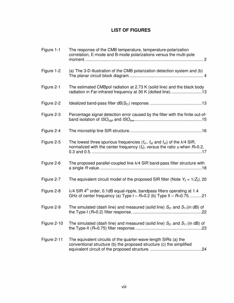
As part of the NASA’s mission to explore the universe, scientists measure the
cosmic microwave background (CMB) polarization at various angular scales as shown in
Figure 1-1. The temperature-temperature angular power spectrum (TT) has been well-
measured and corresponds to the density anisotropies that provide the seeds for
structure formation later in the universe’s history. The polarization is just now beginning
to be explored and is believed to be present in two modes: the E-modes and the B-
modes. The former represents those polarization patterns that are curl-free and can be
generated from the same anisotropies that produce the TT spectrum. Conversely, the
latter represents those polarization patterns that are divergence-free and can only be
produced by gravitational waves created by a hypothesized period of exponential
expansion early in the universe’s history referred to as “inflation”. The discovery of the B-
2
modes would provide solid evidence for inflation, and for this reason, they are highly
anticipated. Current technologies have enabled the measurement of the (unpolarized)
CMB temperature anisotropy, temperature-polarization correlation and E-mode
polarization using the Wilkinson Microwave Anisotropic Probe (WMAP) (NASA 2005). At
this point, WMAP and other instruments have placed and reported upper limits on the
presence of CMB B-mode polarization. The minimum detectable signal is limited by
number of channels, time and economic of running the instrument. To address these
practical issues, the next generation of instruments will employ large arrays of
incoherent detectors to achieve the required sensitivity.
Figure 1-1 The response of the CMB temperature, temperature-polarization correlation, E-mode and B-mode polarizations versus the multi-pole moment.
To detect the B-mode polarization, which has the temperature fluctuation of 0.02
µK, a direct detection system that can operate at 0.1 K or lower must be developed. At

3
this temperature range, the system benefits from the proper operation of passive
superconducting microwave components and sensitive superconducting microwave
detectors. These components will produce lower background noise than active amplifiers
because the background noise is limited to the thermal noise at their operating
temperature.
This dissertation focuses on the development of design techniques used to
produce high-performance microwave planar bandpass filters and magic-Ts. These
filters and magic-Ts are constituents of the direct detection system that will be used to
search for the B-mode microwave cosmic background polarization in the frequency
range from 27.5 GHz to 150 GHz. The use of direct detectors (e.g. transition-edge
sensors) allows the system noise to be limited by the quantum fluctuations in the 2.725
K CMB. To increase the sensitivity of a background limited instrument, it is necessary to
employ multiple detectors. Each detector shown in Figure 1-2(a) consists of a corrugated
circular waveguide terminated with a quarter wavelength (λ/4) backshort. Microwave
energy in the waveguide is collected at the orthomode transducer (OMT), a part of the
planar detecting circuit, and transferred to other microstrip circuits. Microstrip circuits are
suitable candidates in this application as opposed to waveguide circuits since several
detector modules can be produced using fewer fabrication steps. Moreover, the modules
are smaller and lighter.
Each detector system consists of several planar circuits such as the OMT,
bandpass filters, magic-Ts, and thermal detectors as shown in Figure 1-2(b). The OMT
is used to extract the horizontal (H) and vertical (V) components of the signals. The
magic-T is used to combine the out-of-phase signals generated by the OMT. The filters
are used to accept the in-band power and reject unwanted out-of-band power. Finally
the signal is received at the thermal detector. The readings from several thermal
detectors are multiplexed to one output line. The digital signal processing (DSP) unit is

4
used to extract the Q and U Stokes parameters from which the desired angular power
spectrum can then be derived.
(a) (b)
Figure 1-2 (a) The 3-D illustration of the CMB polarization detection system and (b) The planar circuit block diagram.
1.2 Filters’ and Magic-Ts’ General Requirements
The filters are used in the direct detection system to provide very broad
attenuation bandwidth and high out-of-band suppression to reject the out-of-band
infrared thermal noise. Sufficient attenuation must be provided up to seven times the

5
filter’s center frequency (f0). This will be discussed in section 2.2. In addition, the filter
must have low in-band insertion loss and must be simple to fabricate.
The magic-Ts are used in the direct detection system to combine the pairs of
vertical and horizontal OMT probes. They must have low loss and very broadband
response to conserve signal power. Moreover, they must have high E-H port isolation to
prevent the generation of higher order modes in the wave guide structure.
To simplify the fabrication process used to produce filters and magic-Ts, it is
desirable that the designs have the minimum number of via holes and metallized layers.
Since the network analyzer used to measure the filter frequency response can operate
up to 40 GHz, all prototypes of the planar bandpass filters were designed at 1.4 GHz, 4
GHz and 33 GHz to be able to observe the spurious frequency response of up to 40
GHz. The magic-T prototypes are designed to operate at 10 GHz and are tested from 5
GHz to 20 GHz.
1.3 Contributions
There are two areas of contribution in this dissertation.
The first is the development of bandpass filters with high out-of-band rejection.
The double split-end stepped impedance resonator and its related structures are
introduced for the first time. The optimal resonator coupling coefficients have been
determined. The broadband bandstop filter has been studied. Its transmission poles and
zeros were derived so that the bandstop filter can be integrated with the bandpass filter
without degrading the in-band response. By combining all of the developed techniques,
the filter simultaneously produces very high out-of-band attenuation and low in-band
insertion loss. This level of out-of-band attenuation and bandwidth has not previously
been reported for planar circuits.

6
The second is the development of the low-loss hybrids. The technique used to
reduce radiation loss in a microstrip-to-slotline transition is introduced for the first time.
The developed planar magic-Ts use the smallest slotline area. As a result, these magic-
Ts have lower insertion loss and higher sum-to-different port isolation, at frequencies
above 5 GHz, than any reported by the prior state-of-the-art broadband planar magic-Ts.
This research produces high-performance filters and magic-Ts that are not only
suitable for use in radio astronomy applications, but also suitable for use in most
microwave systems. Moreover, the fabrication of both filters and magic-T requires few
metallized layers. The filter and magic-T designs also require no via holes, bondwires or
air-bridges, which significantly reduce their fabrication complexity.

7
CHAPTER 2
2 FILTER DESIGN WITH HIGH OUT-OF-BAND PERFORMANCE
2.1 Literature Review
Microwave filter design has been a subject of interest for several decades.
Several planar filter designs satisfy most of the requirements around the filter pass-band
(Hong and Lancaster 1996; Liang, Shih et al. 1999; Kuo and Cheng 2004; Chang and
Tam 2005). However their out-of-band performance is often limited. Since the filter is
fundamentally made of sections of transmission line to imitate the ideal lumped-element
filter response, the in-band response of the filter is roughly reproduced out-of-band
because of the transmission line’s periodic property (Pozar 1997).
The out-of-band characteristic of the filter is also dependent on the order of the
filter, pass-band bandwidth and the separation between the fundamental frequency and
the lowest spurious resonance mode of the filter (Matthaei, Young et al. 1980).
To obtain the filter with wide stop-band and high stop-band attenuation, several
techniques have been developed. These techniques are generally fall into three
categories. One is to alter the transmission line periodicity. Second is to design filters
with stepped impedance resonators. Third, the techniques use the transmission line
periodicity to suppress the filter’s spurious frequency response. Finally, the filter can be
embedded with dissipative elements to suppress the out-of-band response.
2.1.1 Transmission Line Periodicity Alteration Techniques
The transmission lines shape is modified to produce discontinuity in transmission
line sections such that it transmits signal in the pass-band but reflects the signal out-of-
band. These techniques are commonly incorporated in resonators in the bandpass filter
8
design such that the filter’s spurious responses are shifted away from the fundamental
frequency.
The level of discontinuities ranges from small discontinuity such as in a wiggly-
line filter (Lopetegi, Laso et al. 2004) and in linear tapered impedance resonators
(Sagawa, Shirai et al. 1993), to large step discontinuity, which requires transmission
lines with slots on a ground plane (Quendo, Rius et al. 2001; Wang and Zhu 2005).
A microstrip line section can also be patterned as in (Chang and Tam 2005),
which produces a transmission zero out-of-band. The transmission pattern on a high-
temperature superconductor can also reduce the physical size of the filter, as it behaves
like a delay line (Lancaster, Huang et al. 1996). Moreover, using lumped elements in the
planar filter design (Swanson 1989) can be considered as producing discontinuity. Since
the inductor and capacitor consist of narrow and wide transmission lines, their series
connection produces a step in conductor width. The semi-lumped-element technique
(Kaddour, Pistono et al. 2004) can also be used. In theory, a lumped element filter
produces filter response with no out-of-band spurs. However, in practical
implementation, lumped elements at high frequency are considered sections of
transmission line and the filters using these elements produce a spurious response.
The stop-band performance of the filter using these techniques is typically limited
to 30 dB for a filter order of less than 3 and with 10 percent of bandwidth. The out-of-
band suppression bandwidth is limited to four times its fundamental frequency.
2.1.2 Filter design using stepped-impedance resonators
To determine the approximate location of the spurious response of the filter,
stepped-impedance resonators (SIRs) are used (Sagawa, Takahashi et al. 1989;
Ishizaki and Uwano 1994; Sagawa, Makimoto et al. 1997; Wada and Awai 1999;
Makimoto and Yamashita 2001; Nam, Lee et al. 2001; Kuo and Shih 2002; Lee, Park et

9
al. 2002; Sanada, Takehara et al. 2002; Uchida, Furukawa et al. 2002; Avrillon, Pele et
al. 2003; Banciu, Ramer et al. 2003; Kuo and Shih 2003; Padhi and Karmakar 2004;
Pang, Ho et al. 2004). The spurious response of the filter using this technique is directly
related to the resonance frequency of the resonator. As the stepped-impedance ratio (R)
of the SIR is reduced, the filter’s stop-band bandwidth is extended (Makimoto and
Yamashita 1980; Kuo and Shih 2003; U-yen, Wollack et al. 2004). The minimum value of
R is set by the limited physical line width of the resonator. The spurious response of the
filter using this technique can be predicted as long as the transmission line propagates in
(or close to) TEM mode at high frequency. There are three types of SIR resonators: full-
wave, half-wave and quarter-wave lengths.
The full-wave SIR has the highest resonance modes of the three types
(Karacaoglu, Robertson et al. 1994; Sagawa, Makimoto et al. 1997). It is typically used
in dual-mode filter design and has no benefit in out-of-band suppression. Moreover, it
has large size.
The half-wave SIR is widely used in bandpass filter designs (Makimoto and
Yamashita 1980; Sagawa, Takahashi et al. 1989; Sagawa, Makimoto et al. 1997; Wada
and Awai 1999; Nam, Lee et al. 2001; Banciu, Ioachim et al. 2002; Kuo and Shih 2002;
Uchida, Furukawa et al. 2002; Avrillon, Pele et al. 2003; Banciu, Ramer et al. 2003; Kuo
and Shih 2003; Kuo, Hsieh et al. 2004; Padhi and Karmakar 2004), since it requires no
ground termination in the resonator. It consists of both odd and even mode resonance
frequencies. The maximum filter’s out of band suppression using this type of SIR is
achieved using the coaxial-line with Saucer-loaded SIRs (Uchida, Furukawa et al. 2002).
The optimal size of the half-wave SIR is determined in (Kuo and Shih 2003). This size
gives the maximum separation between the fundamental frequency and its lowest
spurious resonance frequency for a given value R, although it does not produce the
minimum size SIR. The optimal-size SIR is used in the filter design and produces a filter

10
with a stop-band bandwidth of 8.4f0 and with a least 32 dB of attenuation (Kuo and Shih
2003).
Finally, the quarter-wave SIR is also used in filter designs (Ishizaki and Uwano
1994; Lee, Park et al. 2002; Sanada, Takehara et al. 2002; Pang, Ho et al. 2004). It has
the smallest physical size and the fewest number of resonance frequency modes since
only odd mode resonance frequencies exist. The optimal size of the quarter-wave SIR is
determined in (Makimoto and Yamashita 1980). It not only gives the broadest separation
of the spurious resonance frequency and its fundamental frequency, but also gives the
smallest resonator size (U-yen, Wollack et al. 2004).
2.1.3 Transmission line techniques used to suppress the filter’s spurious response
Transmission zeros can be integrated into the filter in the form of quarter-wave
length transmission line opened-end (Wong 1979) or stepped-impedance line opened-
end (Kuo, Hsieh et al. 2004). In planar coupled-SIR filters, transmission zeros are
incorporated in the end sections of the filter in the form of tapped resonator (Kuo and
Shih 2003) or spur line structure (Pang, Ho et al. 2004). They are inserted in the middle
section of the resonators in (Kuo, Hsieh et al. 2004). They can also be embedded in the
transmission line (Chang and Tam 2005). The transmission zero can also be integrated
inside the resonator through anti-parallel coupling (Matsuo, Yabuki et al. 2000) ,
conventional parallel coupling, or the impedance transformation technique (Wada and
Awai 1999).
2.1.4 The filter design embedded with dissipative elements to suppress out-of-band
response.
Dissipative elements can be inserted in the filter to suppress out-of-band
spurious responses. The dissipative elements can be in the form of a resistor (Lee, Ryu

11
et al. 2002) or a large slot on the ground plane (Kim, Kim et al. 2004). Although using a
resistor can suppress spurious frequency responses by approximately 25 dB, it
produces an additional 0.5 dB of insertion loss in-band. The dissipative element using a
slot on a large ground plane does not contribute much loss at low frequency; however,
its out-of-band radiation loss increases in-band insertion loss as the filter’s operating
frequency increases. In conclusion, the dissipative techniques can be used with limited
slot size on a ground plane to minimize in-band insertion loss. Resistive elements should
not be used in low-loss filter designs.
2.2 Filter’s Out-of-band Requirement for Radio Astronomy Applications
In radio astronomy applications, the microwave filter is one of the many important
components in the system, since it suppresses out-of-band noise/inference and
determines the quality of the received signal. The ultimate research goal is to design
low-loss filters for this application at 100 GHz and operate them at 4 Kelvin. The current
research aims to develop a scaled prototype at lower frequency.
The required specifications of the filter for this application are set by the required
accuracy of the instrument. The filter will be used at the front end of the instrument to
detect Comic Microwave Background Polarization (CMBPol) radiation. This radiation is
used to study the expansion of the universe from the Big Bang (Haig 1998). The energy
spectrum of the CMBpol can be estimated accurately by the Plank’s black body radiation
equation per unit volume per unit frequency as follows:
( )
−
=
1
8,
3
3
kT
hfblkbody
ec
hfTfP
π
.
(2-1)

12
where c is the velocity of light in vacuum and is equal to 3×10⁸ m/s. h is the Plank’s
constant and is equal to 6.626 ×10⁻³⁴ m2kg/s and k is the Boltzmann’s constant and is
equal to 1.38×10⁻²³ Joules/K. T is the temperature of the black body in Kelvin. The
CMBpol’s radiating temperature is 2.725 Kelvin (K). It will be measured with the
presence of the sun’s far-infrared radiation at ~30K ranging from 300 to 600 GHz. The
overall energy spectrum is shown in Figure 2-1. Since the sun’s infrared power is at least
30 dB higher than that of the CMBpol’s, it produces strong out-of-band interference,
which can significantly degrade the detecting signal quality.
The CMBpol detector, operating at the frequency ranging from 80 to 120 GHz,
requires low-loss bandpass filter with wide stop-band bandwidth and with an attenuation
to reject the infrared interference. Since the planar filter for this application is made of
Niobium (Nb) superconductor on dielectric substrate. The minimum stop-band bandwidth
of the filter is set by the cut-off frequency of the Nb superconductor (fc) at ~700 GHz,
where the Nb superconductor becomes normal metal and produces high signal
attenuation above 700 GHz.
To investigate the error caused by the strong interference, the integral power at
the detector is measured and compared with the ideal receiving power. The filter used in
this investigation is assumed to have ideal transition from pass-band to stop-band and
has infinite stop-band bandwidth. The low-frequency side stop-band isolation (ISOlow)
and high-frequency side stop-band isolation (ISOhigh) are defined relative to the in-band
insertion loss, as shown in Figure 2-2.

13
Figure 2-1 The estimated CMBpol radiation at 2.73 K (solid line) and the black body radiation in Far-infrared frequency at 30 K (dotted line).
dB|S
21|
Figure 2-2 Idealized band-pass filter dB|S21| response.

14
The amount of detected power is the integral of radiation energy for the entire
frequency spectrum as follows:
( ) ( )∫=high
low
f
f
highlowect TfPblkbodyffTP ,,,det . (2-2)
The percentage reading error can be defined as the difference between the ideal and the
actual detected power as follows:
100% ⋅−
=ideal
idealactual
P
PPerror
(2-3)
where the ideal detected power is
( )∫ ⋅==2
1
73.2,f
f
blkbodyideal dfKTfPP
. (2-4)
And the actual detected power is
( ) ( )
( ) ( )
⋅=+⋅=⋅
+⋅=+⋅==
∫ ∫
∫∫
∞
2
12
1
600
300
0
30,73.2,
73.2,73.2,
f
GHz
GHz
blkbodyblkbodyhigh
f
blkbodylow
f
f
blkbodyactual
dfKTfPdfKTfPISO
dfKTfPISOdfKTfPP
.
(2-5)
The percentage error can be plotted as a function of ISOlow and ISOhigh as shown
in Figure 2-3. From Figure 2-3, we observed that the out-of-band interference has a
strong influence on signal detection error. To achieve a percentage error of less than 1
percent, the ISOhigh should be more than 55 dB and the ISOlow is more than 30 dB. This
requirement set the specification of the bandpass filter used for this application.

15
Percentage error
Figure 2-3 Percentage signal detection error caused by the filter with the finite out-of-band isolation of ISOhigh and ISOlow.
2.3 Quarter-wave SIR Spurious Characteristics and Its Optimal Length
The λ/4 SIR has a superior spurious response than other types of SIR. Its size is
smaller and the resonator excites fewer spurious frequency modes. The minimum size of
this resonator has been determined as well as it spurious responses in (Sagawa,
Makimoto et al. 1985), however no literature has been reported regarding the optimum
λ/4 SIR length that provides maximum spurious-free bandwidth.
This section explains the detail of the λ/4 SIR spurious resonance mode and the
optimal resonator length that maximize the filter’s spurious-free bandwidth. From a λ/4
SIR shown in Figure 2-4, the input admittance at the opened- end side can be derived as
follows:

16
Figure 2-4 The microstrip line SIR structure.
)tan()tan(
)tan()tan(
21
212
θθ
θθ
R
RYjYin
+
−⋅=
(2-6)
Where:
θ1 : an electrical length of the transmission line Z1,
θ2 : an electrical length of the transmission line
Z2=1/Y2,
Yin : input admittance from the opened end of the
resonator,
Zin : input impedance from the grounded end,
R : the stepped impedance ratio Z2/Z1.
When Yin equals to 0, the resonance condition is as shown in (2-7).
( ) ( )21
1
2 tantan θθ==Z
ZR
(2-7)
Since there is only one resonance conditions in (2-6) when the nominator of (2-6) equals
0, the number of spurious frequencies is minimized and shifted away from the
fundamental frequency. The optimal length of the resonator for the most extend spurious
frequency can be determined by root searching technique. By defining the ratio
u=θ2/(θ1+θ2) with the value of R ranging from 0 to 1 (Kuo and Shih 2003), the normalized
spurious response can be determined according to the scaling of the SIR line length as
shown in Figure 2-5. It is found that the spurious response of the λ/4 SIR is symmetric

17
and the second resonance (or the first spurious) frequency is maximized when u=0.5
(i.e. θ1=θ2=θ0) for all R greater than 0. This is the similar condition that produces the
smallest resonator length. When R equals 0 or 1, the SIR becomes a uniform quarter-
wave impedance resonator and its normalized resonances are positive odd numbers.
2
4
6
8
10
12
14
0 0.2 0.4 0.6 0.8 1
u
No
rma
lize
d S
pu
riou
s F
req
uen
cy
R =0.2
R =0.3
R =0.5
Figure 2-5 The lowest three spurious frequencies (fs1, fs2 and fs3) of the λ/4 SIR, normalized with the center frequency (f0), versus the ratio u when R=0.2, 0.3 and 0.5.
2.4 Parallel-coupled λλλλ/4 SIR Bandpass Filter
To construct a compact λ/4 microstrip SIR filter, SIRs are parallel coupled as
shown in Figure 2-6. There are two canonical coupled line circuits on the SIR. The
opened-end and the short-end parallel coupling sections are used one after another as
shown in the circuit model in Figure 2-7. In this design, the optimum λ/4 SIR length is
chosen as discussed above. The coupler can be modeled as either the admittance
inverter (K) or impedance inverter (J). To compute J and K, the susceptance slope (b)
fs1/f0
fs2/f0
fs3/f0

18
and admittance slope (a) of the λ/4 SIR are required. These parameters can be
calculated based on (Matthaei, Young et al. 1980). The parameters b and a can be
derived as follows:
Figure 2-6 The proposed parallel-coupled line λ/4 SIR band-pass filter structure with a single R value.
( )20
21
2
0
2
20
0
0 )tan(12
220
YYY
Y
d
dBb θ
θθ
θ
θ
θθ
=+
+⋅==
= (2-8)
( )10
21
2
0
2
10
0
0 )tan(12
220
ZZZ
Z
d
dXa θ
θθ
θ
θ
θθ
=+
+⋅==
= (2-9)
where susceptance (B) and reactance (X) are imaginary parts of Yin and Zin from Figure
2-4.
In the design of an N-stage band-pass filter, all SIRs have the same R (Z1 and
Z2) in all stages as shown in Figure 2-6. The short-end coupled line is used at the first
and the last section of the filter, since most applications require same impedance
termination at both input and output (i.e. Z1=Z0). Moreover, the coupling gap of the high
impedance coupled line in those sections can be designed with ease without reaching

19
the fabrication tolerance limitation. Using (2-8) and (2-9), the impedance and the
admittance invertor of coupling sections can be calculated as follow:
10
0
1
10
11
1,0gg
wZ
gg
ZwaK
θ==
(2-10a)
12
0
1
1
2
1,
++
++ ==
iiii
iiii
ggZ
w
gg
bbwJ
θ
(2-10b)
1
10
1
1
2
1,
++
+
+ ==jjjj
jj
jjgg
Zw
gg
aawK
θ
(2-10c)
1
01
1
11,
++
+ ==NNNN
NNN
gg
wZ
gg
ZwaK
θ
(2-10d)
where i and j are odd and even numbers between 1 and N-1, respectively; w is the
fractional bandwidth of the center frequency. gi and gj are the filter coefficients of section
i and j, respectively. Odd and even mode impedance and admittance of coupled lines
can be determined based on (Makimoto and Yamashita 1980) as follows:
( ) ( )( ) ( )22
0
2
000,0
cot1
sin1
θ
θ
JZ
JZJZZZ e
−
++=
(2-11a)
( ) ( )( ) ( )22
0
2
000,0
cot1
sin1
θ
θ
JZ
JZJZZZ o
−
+−=
(2-11b)
for the coupled line with opened-end termination and
( ) ( )( ) ( )22
0
2
000,0
cot1
sin1
θ
θ
KY
KYKYYY e
−
+−=
(2-12a)
( ) ( )( ) ( )22
0
2
000,0
cot1
sin1
θ
θ
KY
KYKYYY o
−
++=
(2-11b)
for the coupled line with grounded-end termination, where Y0,e=1/Z0,e and Y0,o=1/Z0,o.

20
J1,2
Y2
K0,1
Z1
Z1 Y
2 K2,3
Z1
Z1
SIR SIR
Open-end parallel coupling
section
Short-end parallel coupling
section
Input
Terminal
0θ 0θ0θ0θ
KN,N+1
Z1
JN-1,N
Y2 Z
1
Output
Terminal
SIR
0θ0θ
Figure 2-7 The equivalent circuit model of the proposed SIR filter (Note Y2 = 1/Z2).
Two bandpass filters are fabricated to demonstrate the proposed technique. The
filters shown in Figure 2-8(a) and (b) are prototypes designed for passive radiometry
systems. The filters have center frequency of 1.412 GHz and have relative bandwidth of
7.5 percent. The initial designed prototypes are based on the 4th order Chebyshev
response with 0.1 dB passband ripple. All design parameters are listed in Table 2-1.
Table 2-1 The design parameters of the bandpass filters
Type - I Type - II Impedance ratio 0.2 0.75 Z1 (Ω) 50 50 Z2 (Ω) 10 37.5 Resonator Length (degree) 48.19 81.786 Slope Parameter a 21.027 35.69 b 0.042 0.019 Even, Odd Mode Impedance (Ω) Z0,e1,Z0,o1 (Z0,e5,Z0,o5) 69.7, 29.75 65.65, 33.80 Z0,e2,Z0,o2 (Z0,e4,Z0,e4) 10.69, 9.40 40.23, 35.12 Z0,e3,Z0,o3 52.54, 47.46 52.69, 47.31

21
(a)
(b)
Figure 2-8 λ/4 SIR 4th order, 0.1 dB equal-ripple, bandpass filters operating at 1.4 GHz of center frequency (a) Type I – R=0.2 (b) Type II – R=0.75.
The filter type I has a step impedance ratio of 0.2, whereas the filter type II has a
step impedance ratio of 0.75. A 0.635 mm-thick Roger’s Duriod 6010 substrate with the
dielectric constant of 10.2 and the loss tangent of 0.0023 is used in both designs. The
parameter R is adjusted based on 50 Ohm characteristic impedance at the input/output
terminal. Type-II filter has u=0.5 whereas the final Type-I filter has u=0.64. The Type-I
filter is not designed with the optimal resonator length (i.e. θ1=θ2=θ0). If the optimal
length is used, the coupled section with opened-end termination will not provide

22
sufficient coupling coefficient for the particular fabrication with minimum allowable metal
spacing of 100 µm. The physical length and SIR spacing of Type-I filter is optimized to
overcome the minimum metal trace spacing restriction. As a result, the first spurious
frequency of the Type-I filter appears at 5.3f0 as opposed to 6.5f0 if u=0.5.
The stop-band attenuation is more than 50 dB up to 4.8f0 for Type-I filter and up
to 3.4f0 for Type-II filter. The spurious frequencies match well with the calculated values
with few percent of error.
From Figure 2-9 and Figure 2-10, the average in-band insertion loss is 4.0 dB for
R=0.2 and 3.0 dB for R=0.75. The in-band insertion loss of Type-I filter is higher than
that of Type-II filter. Since Type-I filter has higher step discontinuity than in the Type-II
filter, the SIRs used in the design of Type-I filter have lower quality factor than those
used in the design of Type-II filter. This increases the in-band insertion loss as
experimentally confirmed in (Kuo and Shih 2003) and (Stracca and Panzeri 1986).
-80
-70
-60
-50
-40
-30
-20
-10
0
1 2 3 4 5 6 7 8
Frequency (GHz)
dB
Figure 2-9 The simulated (dash line) and measured (solid line) S21 and S11(in dB) of the Type-I (R=0.2) filter response.

23
-80
-70
-60
-50
-40
-30
-20
-10
0
1 2 3 4 5 6 7 8 9 10
Frequency (GHz)
dB
Figure 2-10 The simulated (dash line) and measured (solid line) S21 and S11 (in dB) of the Type-II (R=0.75) filter response.
2.5 Double Split-end Quarter-wave Stepped Impedance Resonator
The λ/4 SIR resonator shown in Figure 2-11(a) has many desirable properties for
use in coupled resonator design. Its size is smaller than that of the half-wave resonator
and produces fewer resonance frequencies. However, due to its small size, it is difficult
to provide sufficient coupling to produce a filter response that requires wide bandwidth.
In this section, a new λ/4 SIR resonator structure is proposed. To overcome the
coupling surface limitation, the grounded and opened ends of the transmission line
section of the resonator can be split and folded perpendicular the structure as shown in
Figure 2-11(b). The unloaded quality factor (Qu) of this resonator is slightly degraded
since it has a larger discontinuity and has narrow lines. The moment method simulation
results show that Qu is reduced from 314 to 294 when compared with the conventional
λ/4 SIR on 0.762mm-thick Roger’s Duriod 6002 substrate when both have R=0.528 and
Z1=50.

24
Figure 2-11 The equivalent circuits of the quarter-wave-length SIRs (a) the conventional structure (b) the proposed structure (c) the simplified equivalent circuit of the proposed structure.
The simplified equivalent circuit is shown in Figure 2-11(c). The electrical lengths
θ1" and θ2" are chosen for the lines with the characteristic impedances 2Z1 and 2Z2,
respectively, such that transmission zeros are generated when coupled to other
resonators (as demonstrated in Section 2.7. θ1' and θ2' are chosen such that θ1=θ1'+θ1"
and θ2=θ2'+θ2". θ1 and θ2 are the electrical lengths in radian of the transmission lines with
the characteristic impedances Z1 and Z2, respectively.
By performing a circuit analysis, it is simple to see that the proposed circuit is
identical to the conventional λ/4 SIR resonator. By ignoring the discontinuity effect, its
resonance frequencies can be derived in (2-7). The condition θ1=θ2=θ0 is used to
maximize the separation between the fundamental frequency and its lowest spurious
resonance frequency. It also gives the shortest resonator length. The fundamental
resonance condition becomes
)(tan 0
2 θ=R (2-13)
Using the double split-end SIRs in filter designs has several advantages over
using the conventional structures. First, it is easier to produce a strong coupling

25
coefficient when two resonators are in-line coupled since more coupling area is available
between two resonators. Second, the filter is more compact. Finally, this coupling
topology introduces an additional transmission zero per coupling section to increase the
out-of-band attenuation. As a result, for a high-order filter where many transmission
zeros are present, the filter may no longer require SIRs with low R value to achieve wide
out-of- band attenuation, as demonstrated in the filter designs in Section 2.8.
2.6 Tapped Quarter-wavelength Resonator
The tapping technique is commonly used in the filter design (Lee, Park et al.
2002; Kuo and Shih 2003; Pang, Ho et al. 2004; Wang and Zhu 2005). Not only does it
eliminate coupling at the end sections of the filter, it also produces extra transmission
zeros and it can be used to reject spurious responses or increase the out-of-band
attenuation levels (Kuo and Shih 2003). This technique was implemented in the λ/4 SIR
filter in (Lee, Park et al. 2002), however no analytical solution has been reported. To
determine the tapping position at the resonator for a given filter coefficent, Qsi is
required.
In this section, the Qsi of an optimal-length λ/4 SIR is determined for the first time.
The tapped λ/4 SIR shown in Figure 2-12(a) is derived based on the condition where
θ1=θ2=θ0 as it greatly simplifies the Qsi equation. The calculation is based on the lossless
transmission line model. From the definition in (Kuo and Shih 2003)
02
0
ωωω
ω
=
=d
dBRQ Lsi
(2-14)

26
Figure 2-12 The tapped quarter-wave-length stepped impedance resonator of (a) the conventional structure and the proposed structure where (b) the tapped location is in the Lo-Z impedance (c) the tapped location is in the Hi-Z impedance.
where B is the total susceptance of the resonator seen by the feed line at the tap point
derived at the band pass filter’s center angular velocity ω0. B, a function of the angular
velocity ω, is the parallel combination of the impedance looking toward the opened-end
and short-end of the resonator from the tapped point. The solution of Qsi is dependent on
the tapping location (electrical length φ), as shown in Figure 2-12(a). These relationships
can be expressed as follows.
2.6.1 Tapping location where 0<φ<θ0
Using the transmission line technique, the susceptance at the tap point of the λ/4
SIR can be derived as follows
( )( ) ( ) ( )[ ] ( ) ( )[ ]
( ) ( )[ ] ( )φφθθ
φφθφθφθ
tantantan
tantan1tantantan1
Im
00
000
1 −−
−−−−+=
=
R
R
Z
YB in
(2-15)
where Yin is the input admittance of the resonator seen at the tapped position in Figure
2-12(a). By assuming the linear relationship between ω and the group velocity of wave

27
traveling in the transmission medium. The Qsi in (2-14) can be rewritten in terms of θ as
follows
( )
02
0
θθθ
θθ
=
=d
dBRQ Lsi . (2-16)
Since φ is also a function of frequency, it is treated as a function of θ in (2-16). By
using (2-7), (2-15) and (2-16), Qsi can be computed and simplified to as follows
( )φ
θ2
1
0
sinZ
RQ L
si = . (2-17)
2.6.2 Tapping location where θ0≤φ≤2θ0
In this case, the tapped location lies on the low-Z section. The Qsi calculation can
be simplified by defining a new variable
φθφ −= 02' . (2-18)
The susceptance at the tap point can be derived as follows
( )( ) ( )( ) ( )
−+
−−+=
'tantan
'tantan'tan
1
00
00
2 φθθ
φθθφ
R
R
ZB . (2-19)
By using (2-7), (2-16) and (2-19), Qsi can be computed and simplified to
( )φθ
θ
−=
0
2
2
0
2cosZ
RQ L
si . (2-20)
The Qsi is plotted versus φ in Figure 2-13. The practical upper bound value of Qsi
(when φ/θ0 =0) is limited by the resonator’s Qu. It is simple to verify the equation (2-17)
and (2-20) by comparing them to the Qsi of the λ/4 uniform resonator in (Wong 1979).
The SIR becomes a uniform impedance resonator (UIR) with R=1 i.e. Z1=Z2=Z0. With
this condition, θ0=π/4, (2-17) and (2-20) are simplified to

28
( )φ
π2
0 sin4021 Z
RQ L
ZZZsi === (2-21)
which is identical to the Qsi equation for the UIR. Note that the Qsi of the SIR is
continuous, however its slope is not. Its derivative has a discontinuity at the transition
where φ=θ0 between Z1 and Z2 and when Z1 is not equal to Z2. The mathematical
derivation for the tapped λ/2 SIR in (Kuo and Shih 2003) does not show continuous
response at the step discontinuity which would suggest an unphysical change in the
power in the system at this value.
0.0 0.5 1.0 1.5 2.00.1
1
10
100
Qsi
φ/θ0
R=0.2
R=0.5
R=1
R=2
R=5
Figure 2-13 The Qsi of a λg/4 SIR versus variable tapping position φ /θ0 for a given R=0.2, 0.5, 1, 2 and 5 and Z1=RL.

29
2.6.3 Transmission zero frequencies generated by the tapped SIR
A transmission zero is created at the frequency where an equivalent short
appears at the tapping point. The first transmission zero frequency from section 2.6.1
and section 2.6.2 respectively can be expressed as a function of center frequency (f0)
and φ as follows.
01, ff ptφ
π= , 0≤φ≤θ0 (2-22a)
( ) 0
0
2,22
ff ptφθ
π
−= , θ0≤φ≤2θ0 (2-22b)
The minimum value of fpt,1 and fpt,2 are limited to πf0/θ0 and πf0/2θ0 using tapping
location in section 2.6.1 and section 2.6.2, respectively. For a given fpt,1 or fpt,2 and Qsi, RL
can be determined. Then the filter’s port impedance Z0 is transformed to RL at the
tapping point using a λ/4 impedance transformation network in Figure 2-14. The above
derivations can be applied to the proposed filter. Two possible tapping configurations are
shown in Figure 2-12(b) and (c).
The tapping technique can be combined with the parallel-coupled λ/4 SIR filter
design technique (U-yen, Wollack et al. 2004) as shown in Figure 2-15. By replacing the
coupling section at the ends of the filter with the tapped section, two transmission zeros
are generated. Each transmission zero is used to suppress one spurious resonance
frequency. The transmission zero generated by tapping from Lo-Z section is placed at
4.24f0 (φ1=21.2º), while the other zero generated by the Hi-Z section is placed at 6.1f0
(φ2= 29.5º) as shown in Figure 2-15. The simulation result verifies that transmission
zeros generated by tapped λ/4 SIR technique produce sharp attenuation at transmission
zero frequencies and improve overall out-of-band attenuation around those frequencies.

30
Figure 2-14 The 3th order bandpass filter using tapped SIR technique at the filter’s end sections and two coupling topologies (a) the grounded-end anti-parallel coupling (b) the opened-end anti-parallel coupling.
Figure 2-15 The simulation results of the microstrip filter with the 3rd order Chebyshev response, R=0.528 and with 10% bandwidth on 0.762 mm-thick Roger’s Duroid 6002
substrate. One uses the paralleled coupled λ/4 SIR (dash line). The other is the parallel
coupled λ/4 SIR with tapped SIR technique that has transmission zeroes each of which overlaps at a peak frequency of the two lowest spurious frequencies (solid line).

31
2.7 Resonator Coupling Topology and Transmission Zero Generation
To introduce transmission zeros to the filter without using additional transmission
line components, resonators are coupled inline as shown in Figure 2-14. This creates an
anti-parallel coupling pair between a pair of resonators. There are two types of coupling
in this filter design. One is the anti-parallel coupling with grounded ends (shown in Figure
2-14(a)) and the other with opened ends (shown in Figure 2-14(b)). The filter design
using opened-end anti-parallel coupling was demonstrated in (Matsuo, Yabuki et al.
2000) to improve out-of-band attenuation close to in-band frequency. However, its effect
in out-of-band attenuation at higher frequencies was not considered.
To study this effect, the sections, shown in Figure 2-14(a) and (b), are separated
from the resonators and each section is terminated at both ends with Z0 as shown in
Figure 2-16(a) and (b), respectively. The effect of transmission line bends is neglected to
simplify the explanation as it has negligible effect on transmission zero frequencies shift.
From Figure 2-16 (a), the transmission line with Ls1 and Lp1 long are equivalent to an
electrical degree θ1' and θ1" at f0, respectively. And from Figure 2-16(b), the transmission
line with Ls2 and Lp2 long are equivalent to electrical degrees θ2' and θ2" at f0,
respectively.
Consider the grounded-end (opened-end) anti-parallel coupling section (in Figure
2-16(a) and (b)), the signal traveling from port 1 to port 2 is suppressed at the frequency
where Lp1 (Lp2) becomes a multiple number of a quarter-wave length long. The grounded
terminals of the anti-parallel coupling section are transformed into Hi-Z or Lo-Z at the
center of the structure around the split location. This blocks the signal traveling between
two ports and creates a transmission zero.

32
These transmission zero frequencies can be expressed as follows
0
1
,1"2
fnf npθ
π=
(2-23a)
0
2
,2"2
fnf npθ
π=
(2-23b)
for the grounded-end and opened-end anti-parallel coupling section respectively, where
n is a natural number.
In practical implementation, n is limited to two in (2-23a) and one in (2-23b). This
is due to parasitic at the coupler ends that causes non-ideal ground/open, thus they no-
longer reflect the signal effectively at frequencies much higher than f0. Moreover, the
level of attenuation at fp1 (or fp2) become less as the coupling gap Sp1 (or Sp2) become
larger and vice versa. Therefore, this technique is very effective if used in the filter with
relative bandwidth greater than three percent where the couplings between resonators
are not weak.

33
-120
-100
-80
-60
-40
-20
1 2 3 4 5 6 7 8 9 10
Frequency (GHz)
dB
-200
-100
0
100
200
300
400
500
600
Degre
e
|S 21|
Phase(S 21)
(a)
-140
-120
-100
-80
-60
-40
-20
0
1 2 3 4 5 6 7 8 9 10Frequency (GHz)
dB
-200
-100
0
100
200
300
400
500
600
Degre
e
|S 21|
Phase(S 21)
(b)
Figure 2-16 The wide-band frequency responses of magnitude (dB) and phase (degree) of the S21 of the anti-parallel coupling section on 0.762 mm-thick Rogers’ Duriod 6002 substrate when compared with the theoretical responses. The theoretical results (solid lines) use ideal opened and grounded termination. The simulation results (dash lines) have taken opened-end and ground via effects into account. Each section is designed to produce a transmission zero that overlaps with the SIR’s spurious resonance frequency at 4f0 or 6f0 where f0=1.412 GHz. (a) Hi-Z grounded-end anti-parallel coupling (b) Lo-Z opened-end anti-parallel coupling.

34
2.8 Filter Construction
To simplify the filter model, we assumed that. Using the assumption that there is
no interaction between the opened-end and the grounded-end coupling sections, each
filter section can be constructed individually and combined to generate the desired filter
response. The filter coefficients are generated from three types of sections. First, the Qsi
at the tapped sections can be calculated based the filter’s coefficients (Kuo and Shih
2003) as follows
w
gg
w
ggQQ NN
extsi110 +===
(2-24)
where gi is the filter’s coefficient ranging from 0 to N.
Second, the opened-end and grounded-end anti-parallel coupling sections are
modeled as impedance inverter (J) and admittance inverter (K), respectively. Based on
(U-yen, Wollack et al. 2004), J and K can be derived as follows
1
0
1
2
+
==ii
ii
gg
w
Z
KJZ
θ
(2-25)
where i is an integer ranges from 1 to N-1. Grounded-end and opened-end anti-parallel
coupling sections are combined in series one after another to produce λ/4 SIR
structures. The even mode (Z0,e) and odd mode (Z0,o) impedance of the grounded-end
and opened-end coupler can be determined. Based on (Matsuo, Yabuki et al. 2000), Z0,e
and Z0,o of the grounded-end anti-parallel coupling section can be derived as follows
1
11
111,0
)"cot(1
)"tan(12
−
+
−=
θ
θ
ZK
ZKZZ e
(2-26a)

35
1
11
111,0
)"cot(1
)"tan(12
−
−
+=
θ
θ
ZK
ZKZZ o
. (2-26b)
Similarly, Z0,e and Z0,o of the opened-end anti-parallel coupling section can be
determined as follows
)"cot(1
)"tan(12
22
222,0
θ
θ
JZ
JZZZ e
−
+=
(2-27a)
)"cot(1
)"tan(12
22
222,0
θ
θ
JZ
JZZZ o
+
−=
. (2-27b)
Since there are N+1 transmission zeros available to suppress spurious responses, there
is design flexibility in choosing the appropriate electrical length θ1" and θ2" of each
coupling section to achieve the out-of-band suppression design goal. In this paper, we
allocate all zeros to suppress the first two spurious resonance frequency modes of the
SIR since they have the strongest influence on the in-band signal quality for typical
communication systems. In addition, using the minimum size SIR (i.e. θ1=θ2=θ0), the
third lowest spurious resonance frequency has the maximum extension (U-yen, Wollack
et al. 2004). Using this approach, the electrical length θ1" and θ2" can be approximately
derived at the fundamental frequency as follows
0
01"
θπ
θπθ
+=
(2-28a)
0
02
2"
θπ
θπθ
−=
. (2-28b)
The exact value θ1" and θ2" to provide the maximum spurious response suppression are
dependent on the filter bandwidth and number of available transmission zeros used to
suppress a spurious resonance frequency mode.

36
Two microstrip filters were constructed based on the design procedures
discussed in the earlier sections. The design prototypes are based on 3rd and 6th order
Chebyshev filter response with 0.1 dB of in-band ripple. Their photographs are shown in
Figure 2-17(a) and (b), respectively. The numbers 1-4 in Figure 2-17(a) and 1-7 in
Figure 2-17(b) represent section numbers in Table 2-2. They are prototypes designed for
the front-end of the passive L-band radiometer. The filters are made from 17µm-thick
copper on 0.762 mm-thick Rogers’ Duroid 6002 substrate. The substrate has a dielectric
constant of 2.94 and has a loss tangent of 0.0012 at 10 GHz. The center frequencies of
both filters are set to 1.41 GHz. Both filters use SIRs with R=0.528, where Z1 is set to 50
Ohm and Z2 is set to 26.4 Ohm. This corresponds to Ws1 = 1.9 mm and Ws2 = 4.7 mm in
all coupling sections. From (2-13), θ0 equals to 36º and the SIR has the lowest three
normalized spurious frequencies of 4, 6 and 9 (U-yen, Wollack et al. 2004). Using (2-
28a) and (2-28b) for θ0 = 36º, we obtain θ1" = 30º and θ2"=22.5º. Using these values and
the filters’ K and J values in Table 2-2, the coupler’s odd and even mode characteristic
impedances in each section are determined as in (2-26a), (2-26b), (2-27a) and (2-27b).
The couplers’ physical dimensions are shown in Table 2-2.

37
Figure 2-17 The photograph of the fabricated circuits (a) Type-I (3rd order) filter; (b) Type-II (6th order) filter.
Table 2-2 The specifications and dimensions of the two experimental filters
Type-I 3rd order filter shown in Figure 2-17(a) Section 1 2 3 4
Type1 (a) (b) (c) (d)
Para-meters
Qsi= 10.315,
φ1=21.7º
K1,2=0.058 , Ls1=1.79mm, Lp1=11.0mm, Wp1=0.49mm, Sp1= 0.64mm, Via diameter=
0.2mm
J2,3=0.058 , Ls2=4.27mm, Lp2=7.49mm, Wp2=1.75mm, Sp2=0.17mm
Qsi=10.315,
φ2=29.0º, Via
diameter=0.8mm
Type-I 6th order filter shown in Figure 2-17(b)
Section 1 2, 6 3, 5 4 7
Type1 (a) (b) (c) (b) (a)
Para-meters Qsi=7.813,
φ1=21.9º
K1,2 = K5,6 = 0.061,
Ls1=2.68mm, Lp1=10.44mm, Wp1=0.51mm, Sp1=0.86mm, Via diameter=
0.2mm
J2,3 = J4,5 = 0.041,
Ls2=4.45mm, Lp2=7.37mm, Wp2=1.78mm, Sp2=0.53mm
K3,4 = 0.039, Ls3=2.85mm,
Lp3=10.16mm, Wp3= 0.52mm, Sp3=1.30mm,
Via diameter=0.2mm
Qsi=7.813,
φ2=29.2º
1 (a) Tapped SIR in the Lo-Z section; (b) grounded-end anti-parallel coupling section; (c) opened-end anti-parallel coupling section; (d) Tapped SIR in the Hi-Z section.

38
By comparing the performance of the proposed filter to the filter with no
transmission zero in the band of interest (U-yen, Wollack et al. 2004) as shown in Figure
2-18, the proposed filter design reduces the maximum spurious level of the filter by at
least 8 dB and improves the overall out-of-band response up to more than 6f0 without
affecting the in-band frequency response.
Figure 2-18 Comparison between the frequency response of dB|S21| of the 3rd order filter design using parallel coupled technique that has no transmission zero (dash line) and that of the proposed filter design (solid line) that has 4 transmission zeros. Both filters are 3rd order filters with w=0.1.

39
Figure 2-19 The measured (solid lines) and simulated (dash lines) frequency response of dB|S21| and dB|S11| of the Type-I filter with 2 transmission zeros placed around the lowest spurious resonance frequency (at 5.65 GHz) and 2 transmission zeros placed around the second lowest spurious resonance frequency (at 8.47 GHz).
The measurement results shown in Figure 2-19 and Figure 2-20 agree well with
the moment method simulation using Ansoft Designer. The connectors are de-
embedded from the measurement. From Table 2-2, the tapping locations in the SIRs at
both ends of the filters are placed differently to optimally minimize the peak of the two
lowest spurious frequencies. For the 3rd order filter, the lowest spurious mode was
suppressed to below 41.7 dB, while the second spurious mode was suppressed to below
27.7 dB. In Type-I filter, it has a minimum in-band insertion loss of 0.6 dB. Although the
two lowest spurious resonance frequency modes of the Type-I filter are suppressed by
the same number of transmission zeros, they have different level of suppression due to
several factors.
First, the lowest spurious resonance frequency is additionally suppressed by the
transmission zero generated by the grounded-end anti-parallel coupling section as it is
located close to the first spur as shown in Figure 2-16(a). Second, at high frequency, the
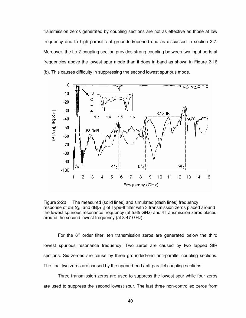
40
transmission zeros generated by coupling sections are not as effective as those at low
frequency due to high parasitic at grounded/opened end as discussed in section 2.7.
Moreover, the Lo-Z coupling section provides strong coupling between two input ports at
frequencies above the lowest spur mode than it does in-band as shown in Figure 2-16
(b). This causes difficulty in suppressing the second lowest spurious mode.
Figure 2-20 The measured (solid lines) and simulated (dash lines) frequency response of dB|S21| and dB|S11| of Type-II filter with 3 transmission zeros placed around the lowest spurious resonance frequency (at 5.65 GHz) and 4 transmission zeros placed around the second lowest frequency (at 8.47 GHz).
For the 6th order filter, ten transmission zeros are generated below the third
lowest spurious resonance frequency. Two zeros are caused by two tapped SIR
sections. Six zeroes are cause by three grounded-end anti-parallel coupling sections.
The final two zeros are caused by the opened-end anti-parallel coupling sections.
Three transmission zeros are used to suppress the lowest spur while four zeros
are used to suppress the second lowest spur. The last three non-controlled zeros from

41
the grounded-end anti-parallel coupling are at frequency lower than the lowest spurious
resonance frequency. As a result, the over-all out-of-band suppression is at least 37.8
dB up to 8.5 times the fundamental frequency. Moreover, the filter has a low in-band
insertion loss of 1.9 dB.
2.9 Filter Design Using Half-wavelength Stepped-impedance Resonator
with Even-mode Spurious Resonance Suppressor
Consider the conventional λ/2 SIR, as shown in Figure 2-21(a), it consists of
three lines. The line in the middle section has the characteristic impedance of Z1. The
others have the characteristic impedance of Z2. At f0, the opened-end of the resonator is
transformed to a virtual ground at the center of the resonator. Then as shown in Figure
2-21(b), both Z1 and Z2 lines are split and folded in perpendicular to its structure to
produce a more compact structure. The split Z1 and Z2 sections have electrical lengths of
θ1″ and θ2″, respectively. As shown in Figure 2-21(c), the SIR’s internal coupling is
formed by inserting SIO stubs around the center. The SIO stub is constructed from two
lines connected in series, each of which has characteristic impedances of Zs1 and Zs2
and electrical lengths of θt1 and θt2, respectively. These electrical lengths are tuned such
that the SIO stub provides a virtual ground at f0. When connected to the parallel line with
the characteristic impedance of 2Z1 in (2-29), it forms a grounded-end anti-parallel
coupler where 2Z1,e and 2Z1,o are its even- and odd-mode characteristic impedance.
oe ZZZ ,1,11 222 ⋅= (2-29)

42
Figure 2-21 The resonator revolution steps (a) the conventional λ/2 SIR (b) the main
resonator: the split-folded λ/2 SIR at center (solid lines) and at sides (dashed line) (c) the
final λ/2 SIR, with stepped impedance stubs inserted, coupled to other SIRs(d) the SIR’s even-mode quarter-circuit model (e) the SIR’s odd-mode quarter-circuit model.
Using the SIO stub allows the lowest even-mode resonance of the SIR to shift
away from f0 as discussed in section 2.9.1. Since the proposed SIR is symmetric in both
x and y axis, it can be modeled using the quarter of the circuit (see the dark gray area in
Figure 2-21(c)) in even and odd modes, as shown in Figure 2-21(d) and Figure 2-21(e),
respectively. The fundamental resonance condition of this SIR is as in (2-7). The
minimum length of the λ/2 SIR is used in this design to reduce the overall filter size (i.e.

43
θ1=θ2=θ0). The split-end sections on the left and the right side of the SIR have the
characteristic impedance of
oe ZZZ ,2,22 222 ⋅= . (2-30)
Where 2Z2,e and 2Z2,o are even- and odd-mode impedance of the opened-end
line 2Z2. They are used for coupling between SIRs to form a filter response. The
admittance inverter for this coupler, which is used for filter designs, is derived in (2-25).
2.9.1 The Resonator’s Spurious Suppression Capability from SIO Stubs
In this filter design is focused on suppressing the lowest spurious resonance
frequency as this filter design will be incorporated with broadband bandstop filter in
section 2.12. The filter’s out-of-band suppression capability depends on two factors.
First, it depends on the R value as it defines the separation between f0 and its lowest
resonance mode. Second, it depends on the SIO stub which has the input impedance as
follows:
( ) ( )( ) ( )12
211
tantan
tantan2
tst
tts
sinR
RZjZs
θθ
θθ
+
−−=
(2-31)
where Rs=Zs2/Zs1. At f0, it behaves as a virtual ground at A-A’ in Figure 2-21(d), thus
Zsin=0. The effect of the variable Rx=Zs1/Z1,e, Rs and us=θt2/(θt1+θt2) on filter responses as
described below.
2.9.2 The Effect of the Rx Variable
The Rx value in SIRs controls the bandwidth of the filter, as well as its out-of-
band suppression capability, given R=Rs.
First, the bandwidth of the filter relies on Rx to be close to zero at f0 in order for
each λ/2 SIR in the filter to behave as two coupled quarter-wavelength (λ/4) SIRs. When
the SIO stub is combined with the main resonator at A-A’ in Figure 2-21(d), a

44
transmission zero frequency (fz) is also generated on the low frequency side of f0 as
shown in Figure 2-22 when Rx=1, 0.2 and 0. fz is formed when the opened end of 2Zs2
line is transformed to a virtual ground at the connection between 2Z1,e and 2Z1 lines. fz
approaches zero as Rx decreases to zero.
Second, the attenuation at the lowest spurious frequency (fs1) of the filter also
relies on the value Rx. As Rx is close to zero, the main resonator behaves close to a λ/4
SIR and its lowest even-mode resonance frequency (fs1) is suppressed.
2.9.3 The Effect of the Rs and us Variable
The Rs and us values can be adjusted such that fs1 of the SIR is shifted away from
f0. The maximum separation between f0 and fs1 is obtained when us=2/3 as well as using
small Rs value. This effect is demonstrated in Figure 2-22 where Rs=1 and us=1 and
where Rs=0.3 and us=2/3.
Figure 2-22 Frequency responses of the dB|S21| of the 4th order filters using the proposed SIRs with R=0.528. The nominal design (bold solid line) has R=Rs=0.528,
Rx=1, θ0=θt1=θt2=36°. Other responses are obtained by only adjusting either Rx (where
R=Rs=0.528 and θt1=θt2=36°) or Rs and us (where Rx=1 and R=0.528) from the nominal design.

45
2.9.4 Filter Design and Implementation
A 4th order bandpass filter can be constructed as shown in Figure 2-23. The
filter’s coefficients are based on an equal-ripple filter prototype. The prototype microstrip
filter has a center frequency at 1.41 GHz and has 10% bandwidth. It will be used in the
NASA’s Aquarius satellite to reject out-of-band spurious response up to 6 GHz while
providing rejection from the on-board radar instrument at 1.265 GHz. A 0.635 mm-thick
Roger’s Duroid 6010 substrate is used in the design. Overall, the filter has a dimension
of 44 mm by 35mm. Its detailed dimension is provided in Table 2-3.
Figure 2-23 The photograph of the 4th order bandpass filter on 0.635 mm-thick Roger’s Duroid 6010 substrate.
The internal spacing (Gs) and the inter-stage spacing (Go) shown in Figure 2-24
are adjusted to provide the proper filter coupling coefficient. Two high impedance λ/4
lines with the line width of Wt1 and Wt2 are tapped from the left and right SIR
respectively. R, Rs and Rx are set to 0.528, 0.3 and 1, respectively, thus θ0=36o, θt1=20o
and θs2=40o. From the given parameters, fs1 of the SIR, the lowest even-mode and odd-
mode frequencies can be determined to be at 3f0 and 4f0, respectively. The line lengths
of Lo1, Lo3 and Lo5 are adjusted such that the coupling sections generate transmission
zeros at 3f0, 3.9f0 and 4f0, respectively, to optimally reject the spurious response of the

46
filter. The line length Ls2 is adjusted in co-ordination with the SIO stubs’ width WL1 and
WL2 such that a transmission zero is generated close to 1.265 GHz. The filter is
designed and simulated using Ansoft Designer. The theoretical result in
Figure 2-25 agrees with the method-of-moments simulation. Using the propose
SIRs alone in filter design can suppress fs1 by more than 20 dB. The filter provides at
least 49 dB of attenuation at 1.265 GHz and has the minimum in-band insertion loss of
1.75 dB, as shown in Figure 2-26. The deviation of the fz value from 1.265 GHz is
caused by asymmetric parasitic couplings from Lo1 and Lo3 to A-A’ and from Lo3 and Lo5
to B-B’ as shown in Figure 2-24, whereas the parasitic coupling between A-A’ and B-B’
has a negligible effect on fz. The proposed filter produces a broadband attenuation of at
least 39.7 dB up to 3.9f0. The suppression around 4.24f0 was as not optimal as in (Kuo
and Shih 2003) due to transmission zeroes slight misplacement.
Figure 2-24 The physical layout with dimensions of the 4th order filter on 0.635 mm-thick Roger’s Duroid 6010 substrate, Z0=50 Ohm.

47
Table 2-3 The Filter’s detail dimension in millimeter
Main resonators SIO stubs & spacing Wo1=1.63, Wo2=4.17,Ws1=0.47, Ws2=1.91, Wt1= 0.11, Wt2=0.1, Lo1=5.36, Lo2=1.24, Lo3=3.78, Lo4= 2.67, Lo5=3.16, Lo6=3.33,
Ls1=0.39, Ls2=Ls3=6.89
WL1=1.71, WL2=7.93, LST1=3.89, LST2=7.17 Gs=0.83,
Go= 2.63
Figure 2-25 The simulated frequency responses of the dB|S21| of the filter in Figure 2-23 with a transmission zero placed around fs1 (solid line) and without transmission zero at fs1 (dashed line). The dotted line is the theoretical filter response using a transmission line model, including a transmission zero at fs1.

48
Figure 2-26 The measured and simulated |S11| and |S21| in dB versus the frequency of the 4th order bandpass filter in Figure 2-23.
2.10 Anti-parallel Stepped-Impedance Opened-end Stub
The structure, called the anti-parallel stepped-impedance (APSI) opened-end
stub, has been implemented in addition to the bandpass filter to reject spurious
responses. The preliminary analysis is performed by (Hsieh and Wang 2005), however
their analysis did not cover the structure’s transmission pole locations. Moreover, their
analysis on the structure’s transmission zero locations is not complete. In this section,
more complete analysis of the APSI opened-end stub is performed such that it can be
sufficiently used as a component in a bandpass filter design to improve the bandpass
filter’s out-of-band performance.
The APSI opened-end stub consists of an anti-parallel coupling pair connected to
a low-impedance transmission line (Z2) open end, as shown in Figure 2-27(a). Z1,e and
Z1,o are the even and odd mode characteristic impedances of the coupler. The coupler

49
has a coupling coefficient of c and is normalized to the characteristic impedance of Z1. θ
is an electrical length of both the Z1 and Z2 section.
Figure 2-27 (a) The physical layout of the APSI stub; and (b) its equivalent circuit.
2.10.1 APSI Opened-end Stub Circuit Modeling and Its Frequency Response
The APSI opened-end stub generates the maximum number of transmission poles
and zeros when its electrical length of the parallel coupling section equals to that of the
low-impedance stub. This condition also simplifies several derivations related to this
structure significantly. The APSI opened-end stub transmission poles and zeros are
shown in Figure 2-28.
Consider the Z matrix equation of a parallel coupled line (Pozar 1997):
=
4
3
2
1
44434241
34333231
24232221
14131211
4
3
2
1
I
I
I
I
ZZZZ
ZZZZ
ZZZZ
ZZZZ
V
V
V
V
(2-32)
Where
( ) ( )θcot2
,1,144332211 oe ZZj
ZZZZ +−
==== (2-33a)

50
( ) ( )θcot2
,1,143342112 oe ZZj
ZZZZ −−
==== (2-33b)
( ) ( )θcsc2
,1,142243113 oe ZZj
ZZZZ −−
==== (2-33c)
( ) ( )θcsc2
,1,132234114 oe ZZj
ZZZZ +−
==== (2-33d)
Z1,e and Z1,o are the even- and odd mode characteristic impedances of the coupler,
respectively. Vi and Ii are voltage and input current at port i, respectively. θ is the
electrical length of both the coupler and the open stub Z2, as shown in Figure 2-27(b). θ
is computed at the center of this structure.
By applying the conditions 43 VV = and ( ))tan(
2433
θj
ZIIV +−= in (2-32), The Z
matrix can be simplified to a two-port matrix
=
2
1
'
22
'
21
'
12
'
11
2
1
I
I
ZZ
ZZ
V
V (2-34)
where
( ) ( )[ ] ( )( ) ( )( )2,1
2
2,12,1,1
2
,1
2
'
22
'
112cossin2
cos22sin
ZZ
ZZZZZZjZZ
e
eeoe
+
−++==
θθ
θθ (2-35a)
( ) ( )[ ] ( )( ) ( )( )2,1
2
2,12,1,1
2
,1
2
'
21
'
122cossin2
cos22sin
ZZ
ZZZZZZjZZ
e
eeoe
+
−+−==
θθ
θθ. (2-35b)
2.10.2 Transmission Zeros Generated by the APSI Opened-end Stub
Transmission zeros are generated around f0 and can derived as follows. Using
the Z matrix transformation to the S-parameter matrix (Pozar 1997), the transmission
zeroes of a structure are determined using the condition
02 0
'
12
21 =∆
=Z
ZZS (2-36)

51
where
( ) 2'
12
2
0
'
11 ZZZZ −+=∆ . (2-37)
Using (2-35b), (2-36) and (2-37), the electrical length, where transmission zeros are
generated, can be determined as follows:.
( )2,1,12,1
2,111,
2
2tan
ZZZZ
ZZn
eoe
ez
+−+=
−πθ (2-38a)
( )2,1,12,1
2,112,
2
2tan
ZZZZ
ZZn
eoe
ez
+−−=
−πθ (2-38b)
2)1(3,
πθ += nz (2-39)
Where n is a positive integer including zero. Consider the fundamental mode where n=0,
from (2-38a), we observe that θz,1 cannot be greater than π/2. By comparing this
structure to the conventional quart-wave length open, we observe that the total length of
this structure is smaller than the conventional opened-end stub when θz,1 is less than
π/4. From (2-38a) and θz,1<π/4 gives
p
oe
oe
e
cZZ
ZZ
Z
Z=
+
−<
,1,1
,1,1
,1
22 (2-40)
where cp is the coupling coefficient of the coupler.
2.10.3 Transmission Poles Generated by the APSI Opened-end Stub
The structure can produce transmission poles at the desired location. Consider
the S11 parameter of the structure using the two-port network conversion table 4.3 in
(Pozar 1997).
( )( )Z
ZZZZZS
∆
−−+=
2'
120
'
110
'
11
11 (2-41)
By substituting (2-35a) and (2-35b) into (2-41) with S11=0 gives.

52
( ) 022tan 2
2
0,1,1
2
0,1
2
,1
2
,1 =−+−− ZZZZZZZZZ xoeeoe θ (2-42)
Solving (2-42) for θ gives the transmission pole location at
( )oe
eoep
ZZ
ZZZZZZn
,12,1
20,1
20,1,121
1,
2tan
−−+=
−πθ (2-43a)
( )oe
eoep
ZZ
ZZZZZZn
,12,1
20,1
20,1,121
2,
2tan
−−−=
−πθ (2-43b)
πθ np =3, (2-44)
We can observe from (2-43a) that θp,1 is valid only when coupler impedance value is
greater than Z0, thus
12 2
,1
0,1,1 +>Z
ZZZZ
e
oe . (2-45)
θp,1, when n=0, can be used to set the required pass-band bandwidth. In addition,
θp,3 always presents in the response and it is independent of the value of the coupler and
the stub impedance.
The frequency response of this structure can be compared with a conventional
stub with the same total electrical length, as shown in Figure 2-29. The APSI opened-
end stub provides significantly higher suppression than the conventional opened-end
stub since three transmission zeroes are concentrated in the same frequency range.
Moreover, low return loss can be obtained in-band with no impedance matching
required.
The signal suppression capability of the APSI stub depends on the separation
between the electrical lengths θz and π-θz. The suppression level becomes higher as θz
and π-θz approach π/2. They can be controlled by independently adjusting the values cp,
Z1 and Z2.

53
-80
-70
-60
-50
-40
-30
-20
-10
0
0 0.5 1 1.5 2
Normalized Frequency
dB
|S11|, d
B|S
21|
dB(S11)
dB(S21)
θp π−θpπ−θzθz π/2 π
2π
θ
dB|S
11|, dB|S
21|
Figure 2-28 The dB|S21| response of the APSI stub and it associated transmission zeros and poles in the fundamental mode where n=0, Z0=50 Ohm, Z1=100 Ohm, cp=0.3 and Z2=50 Ohm.
Figure 2-29 The frequency response of the conventional opened-end stub and the APSI stub. Both have the same total electrical length.

54
2.10.4 High-frequency Blocking Filter Implementation
A band-stop filter can be constructed based on APSI opened-end stubs. Several
sections of the ASPI opened-end stubs can be combined in series, as shown in Figure
2-30. This filter consists of four APSI opened-end stubs with variable Z2 and θ such that
the combined response provides the minimum out-of-band rejection of 50 dB.
0
-50
-100
-150
-2000 10 20 30 40 50
0.45mm
(Black line)
(Pink line)
(green
line)
1
2
Section 1Section 2
Section 3
Frequency (GHz)
|S21| of section 1
|S21| of section 2
|S21| of section 3dB
Overall |S21| response
Overall |S11|
response
0.45mm
0.45mm
Figure 2-30 The high-frequency blocking filter constructed using four sections of the
APSI opened-end stub on 30 µm-thick silicon substrate.

55
The filter is designed based on the Niobium superconductor line on a 30 µm-thick
silicon substrate. The EM simulation shows that the multiple circuit models of the APSI
opened-end stubs can roughly predict the response of the overall bandstop filter as
shown in Figure 2-31. The deviations from the circuit model are due to the parasitic
caused by step discontinuities in the structure. The isolation of the filter is limited by the
physical separation between the two ports of an APSI opened-end stub. Moreover,
spurious responses can be observed when APSI opened-end stubs are serially
connected although the response level is more than 30 dB below the pass-band. These
are caused by the resonance frequencies between several pairs of APSI stubs. Since
the filter is designed to provide high-frequency blocking from 3 GHz to 30 GHz, it was
not optimized for uniform in-band response.
-120
-100
-80
-60
-40
-20
0
0 10 20 30 40 50
Frequency (GHz)
dB
|S11|, d
B|S
21|
EM Simulation dB|S21| EM simulation dB|S11| Ideal response dB|S21|EM simulation dB|S11|EM simulation dB|S21| Ideal response dB|S21|
Figure 2-31 The frequency response of the high-frequency blocking filter using the method of moments simulation (solid line) and the ideal transmission line model (dashed line).

56
2.11 Superconductor Modeling for Use in EM Simulators
The EM simulator is a very important tool used in the microwave circuit designs.
With proper setup, the simulator gives accurate solutions that agree well with the
measurement results. Since almost all simulators are designed for the circuits using
normal metal, some modifications must be applied to the circuit using superconductor. In
this section, proper superconducting transmission line model is introduced in a method
of moment circuit simulator to compensate for kinetic inductance terms in
superconductor. The effect of kinetic inductance in the bandpass filter response is
studied.
Superconductor was discovered in 1911 by H. Kamerlingh Onnes. Its loss less
property is being used in modern microwave instruments to reduce loss in their systems.
In superconductivity, electrons are paired and travel under the influence of electric field
with no loss (Lancaster 1977). The classical superconductor model is the “two fluid
model”, consisting of normal and complex conductivity terms. The complex conductivity
term influences superconducting devices that operate in microwave or sub-mm
frequencies, since It causes the superconducting transmission line to be more inductive
than the normal transmission line. The inductive term in superconductor is known as
kinetic inductance. It is dependent of the London penetration depth (λL), the conductor
thickeness (t), width-to-height ratio of the microstrip line and the substrate’s dielectric
constant (Yassin and Withington 1995).

57
In this dissertation, Niobium (Nb) superconductor on the 1.5 µm thick Al2O3
substrate is used in the filer designs. λL is approximately 90nm at 0 K and it is
comparable to t of 0.1µm. The critical temperature (Tc) is approximately 9.3 K. The
characteristic impedance of the superconducting microstrip line was derived using the
analytical solutions (Yassin and Withington 1995) provided in the appendix. It is
compared with the characteristic impedance and its phase constant of the microstrip line
using loss less metal as shown in Figure 2-32 and Figure 2-33, respectively. The
percentage variation in characteristic impedance is shown in Figure 2-34.
Figure 2-32 The characteristic impedance of the microstrip line using Niobium
superconductor (solid line) and loss-less metal (dashed line) on 1.5 µm thick Al2O3
substrate. The line width varies from 1 to 100 µm. For λL=90 nm, t=0.1 µm and temperature = 4.2 K.

58
Frequency (GHz)
10 20 30 40 500
1000
Ph
ase C
on
sta
nt (r
adia
n/m
ete
r)
3000
500
1500
2000
2500
3500
Nb superconductor
Loss-less conductor
Figure 2-33 Phase constant versus frequency of the Nb superconducting line with line
width of 6 µm.
Width ( m)
20 40 60 80 1004
4.5
5
6
5.5
Figure 2-34 The percentage variation of the microstrip line’s characteristic impedance using Nb superconductor and that using loss less conductor.

59
From Figure 2-34, we observed that the superconducting microstrip characteristic
impedance is approximately 5% higher than that of the loss less microstrip line.
Moreover, the phase constant of the superconductor microstrip line is higher that of the
loss less case due to kinetic inductance effect (Lancaster 1977) as shown in Figure
2-33. In filter responses, this effect causes a shift in its center frequency as well as a
reduction in in-band return loss. For the EM simulator to predict the filter response
accurately, a parameter to compensate for the kinetic inductance is required. The
compensation using surface impedance technique (Kerr 1999) is used since this
technique provides the parameter that can be combined with the available commercial
EM simulation software such as HFSS and Designer from Ansoft Corporation.
In the superconducting fabrication process at NASA GSFC, t is not much greater
than λL. The field incident wave on conductor close to the substrate is more than that on
the other side of the conductor. In this case, the surface impedance equation, where the
incident wave is excited on one side of the conductor plane, is used as follows
LL
LL
t
L
L
t
t
L
L
t
Ls
ejZ
jZe
ejZ
jZe
jZ
λ
η
ηλ
λ
η
ηλ
ωµλ
ωµλ
ωµλ
ωµλ
ωµλ−
−
+
−−
+
−+
=
(2-46)
where Zη is the characteristic impedance of space (377 ohm in vacuum). In this
fabrication process,
2.119377
10
===
=rr
Z
ε
ηεε
µ
(2-47)
λL is also a function of the temperature as follows

60
2
0
1
)(
−
=
Tc
T
TL
λλ
(2-48)
where λ0 is the penetration depth at 0 Kelvin. T is the operating temperature.
Using (2-47), (2-48) and (2-49), the surface impedance is computed as a function of
frequency. Since the surface impedance only has the imaginary part, it is called surface
reactance as shown in Figure 2-35.
Figure 2-35 The frequency response of the surface reactance of the microstrip line versus frequency.
From Figure 2-35, the compensation due to the kinetic inductance can be neglected at
frequency below 1 GHz. However at frequency above microwave, the compensation is
required and can be included in the simulator as sheet impedance. At 4 GHz and 33
GHz, sheet impedance are j2.3×10-3 and j0.019 Ohm, respectively.

61
The EM simulations with and without sheet impedance compensation are
compared with the result obtained from (Yassin and Withington 1995). Ansoft Designer,
which is a method of moment simulator, is used in this evaluation. The results in Figure
2-36 show a very good agreement with the analytical solutions. However, the
characteristic impedance shown in Figure 2-37 agrees within 6% from the predicted
value for the line width ranges from 1 µm to 30 µm.
0
2
4
6
8
10
12
14
16
18
20
0 10 20 30 40 50
Frequency (GHz)
Ph
ase
(de
gre
e)
Simulated loss-less line
Modeled Ioss-less line
Simulated loss-less Line with Kineticinductance compensationModeled Nb Line with Kineticinductance
Figure 2-36 The comparison between the microstrip line phase delay obtained from the EM simulation (dashed lines) and that derived from equations in (Yassin and
Withington 1995) (solid lines). The Nb line is 100 µm long with λ0=90 nm, t=0.1 µm,
T=4.2 K. The Al2O3 dielectric thickness = 1.5 µm and εr=10.

62
0
10
20
30
40
50
60
70
0 5 10 15 20 25 30 35 40 45 50
Width (Micron)
EM Simulation
Superconducting Model
Figure 2-37 The characteristic impedance in Ohm of the Nb superconducting microstrip line obtained by the EM simulation and that from the analytical solution.
The kinetic compensation was included in the 33 GHz bandpass filter design that
will be discussed in section 2.12. The EM simulation results in Figure 2-38 show that the
pass-band filter response without compensation is significantly altered from the original
design with the compensation.
In the pass-band response, the bandwidth of the filter without the compensation
has a broader bandwidth as the transmission line becomes effectively longer due to
smaller phase velocity value; given both filters have the same physical dimensions.
Therefore the electrical length of the couple sections in the filter becomes longer and
produces stronger coupling in the passband. Moreover, the in-band return loss increases
in the filter model with out kinetic inductance compensation due to improper coupling
filter coefficient generated in-band.

63
-100
-90
-80
-70
-60
-50
-40
-30
-20
-10
0
10 20 30 40 50 60
Frequency (GHz)
dB
|S1
1|, d
B|S
21| |S 21|
|S 11|
With kinetic inductance compensation
Without kinetic inductance compensation
Figure 2-38 The pass-band frequency response of the 33 GHz bandpass filter in Figure 2-47(b) with and without the kinetic inductance compensation in the microstrip lines.
In the out-of-band response, changes in the kinetic inductance result in the
variation in the effective electrical length of the filter. This causes shifts in non-optimum
locations of the transmission zeros to suppress the out-of-band spurious responses.
Since the bandpass filter used in the final design has integrated bandstop filters that are
used to suppress spurious response over wide frequency range, non-optimal location of
the transmission zeros have little effect in suppressing the out-of-band response as
shown in Figure 2-39.

64
-120
-100
-80
-60
-40
-20
0
0 50 100 150 200 250 300 350 400
Frequency (GHz)
dB
|S1
1|, d
B|S
21|
With kinetic inductance compensation
Without kinetic inductance compensation
|S 21|
|S 11|
Figure 2-39 The out-of-band frequency response of the 33 GHz bandpass filter in Figure 2-47(b) with and without the kinetic inductance compensation in the microstrip lines.
In conclusion, the compensation of kinetic inductance using sheet impedance
model can accurately predict the propagation constant of the superconducting line.
However, the method of moment simulation shows a small variation of characteristic
impedance from the analytical solution. The kinetic inductance compensation becomes
more important as the filter’s center frequency increases. The pass-band response has
strong effect in this compensation while the out-of-band has negligible effect for the
bandpass filter design with proper out-of-band spur suppression techniques such as the
one discussed in section 2.12.

65
2.12 The Bandstop Filter and Bandpass Filter Integration
In this dissertation, the ultimate goal is to construct the bandpass filter with very
high out-of-band performance. Moreover, the filter design must be compatible with the
provided superconductor fabrication process at NASA Goddard Space Flight Center
(GSFC) such that it is cost effective and qualified for use in the NASA missions. The out-
of-band specifications, discussed in section 1.2, require that the filter provides at least 50
dB of attenuation up to 700 GHz for the filter with f0 of 100 GHz. Moreover, the lowest
possible number of SIRs should be used in a filter design to minimize insertion loss and
to produce a compact filter layout. In this section, a circuit model is developed to design
filters with f0 of 4 GHz and 33 GHz. The 4 GHz filter is designed to demonstrate the out-
of-band suppression capability while the 33 GHz filter is one of the designs to be used in
the CMBpol detector system.
In the narrow band filter where the bandwidth is less than 15%, spurious
responses produced by the filter can be suppressed using transmission zeroes
generated by the SIRs as described in section 2.7. However, in the broadband filter
where the bandwidth is greater than 15%, these spurs are more difficult to suppress as
the isolation between f0 and fs1 decreases in proportion to the filter bandwidth as shown
in Figure 2-40.
From Figure 2-40, the isolation between f0 and fs1 is reduced by 14 dB with the
percentage pass-band bandwidth increases from 0.1 to 0.2. Therefore transmission
zeros generated by the SIRs must also be used to increase the isolation between f0 and
fs1 to an acceptable level. Since, the notch responses created by the transmission zeros
from SIRs are narrow band, more than one transmission zeros are required to
suppression the spurious response and enhance isolation, simultaneously. Using the
Nth order DSOE filter that has N+1 transmission zeros can not sufficiently suppress fs1

66
Figure 2-40 The frequency response of |S21| of the circuit-modeled 3th-order coupled-
λ/4 SIRs filter with R=0.528 in Figure 2-15. They are designed for three different percentage bandwidths (w).
and fs2 or increase the overall isolation, when the value N is small. Therefore additional
zeros are required out-of-band and these zeros can be obtained by inserting bandstop
filters. The bandstop filters consists of APSI opened-end stub combined in series as
discussed in section 2.10.4.
The integration of the bandstop filter with the bandpass filter has several benefits.
First, the out-of-band response of the bandpass filter design can be relaxed, since the
bandstop filter suppresses the out-of-band spurious response more effectively than the
notch responses produced internally by the SIRs in the bandpass filter. Therefore, these
internal notches are no longer needed to be exactly overlapped with the spurious
response at fs1 or at fs2. As a result, the broadband bandpass filter can be designed
using fewer resonators and some transmission zeros from the bandpass filter can be
used to suppress interference close to in band. Second, the bandstop filter allows the
f0 fs
-35
-30
-25
-20
-15
-10
-5
0
0.5 1 1.5 2 2.5 3 3.5 4 4.5Normalized Frequency
dB
|S2
1|
W=0.1
W=0.2
W=0.3Increasing w
fs1

67
attenuation bandwidth to be extended beyond fs2 without affecting the filter’s in-band
response. The bandstop filter can be designed to generate a transmission pole around f0
and three transmission zeros at the frequency beyond f0. Therefore it can be connected
directly in series with the bandpass filter. Additional loss produced by the bandstop filter
is less than the loss in the filter with higher order.
2.12.1 The Bandpass Filter Design Using Integrated Broadband Bandstop Filter
To design the filter that meets both in-band and out-of-band requirements, the
filter has the dependent in-band and out-of-band specifications.
For the In-band specification, the bandpass filter must be designed such that fs1
is furthest away from f0 such that it overlaps with the lowest notch frequency produced
by broadband bandstop filter. f0 is also required to be overlapped with the transmission
pole of the bandstop filter such that the bandpass filter’s pass band response is not
effected. This can be demonstrated in Figure 2-41.
For the out-of-band specification, the minimum number of stages of bandstop
filters is used to minimize the in-band insertion loss. The number of stages is also
dependent on the suppression bandwidth and the level of attenuation.
2.12.2 Bandpass Filter Design
The prototype Chebyshev 4th order filter with 20% bandwidth was designed using
the λ/2 SIR with R of 0.528 where θ1=θ2=θ0. This SIR generates spurious resonance
frequencies at fs1=2.5f0, fs2=4f0, fs3=5f0 and fs4=6f0. The filter with 0.1 dB pass-band ripple
has the coefficient as follows: g0=1, g1=1.1088, g2=1.3061, g3=1.7703, g4=0.8180,
g5=1.3554.

68
dB|S
21|, dB|S
11|
f0 fs1 fs2
fn2fn1 fn3
Out-of-band frequency coverage
In-band frequency
coverage
dB|S
21|
S21
S11
(a)
(b)
fs3
Figure 2-41 The in-band and out-of-band coverage of the bandstop filter for use in bandpass filter integration (a) bandpass filter frequency response (b) bandstop filter frequency response.
The λ/2 SIRs are used as opposed to the λ/4 SIRs to avoid via holes connected
from traces to ground, although they generates additional spurious resonance
frequencies. Using via-less design increases the superconductor fabrication yield and
reduces number of fabrication's photo lithography steps. The filter is designed based on
the procedure discussed in section 2.8. However, the odd and even-mode characteristic
impedances of the grounded-end anti-parallel coupling section are computed using the
following equations
1
11
111,1
)"cot(1
)"tan(1−
+
−=
θ
θ
ZK
ZKZZ e
(2-49)
1
11
111,1
)"cot(1
)"tan(1−
−
+=
θ
θ
ZK
ZKZZ o
(2-50)

69
where K is computed in (2-10c). And the odd and even-mode characteristic impedances
of the opened-end anti-parallel coupling section are computed using the following
equations
)"cot(1
)"tan(1
22
222,2
θ
θ
JZ
JZZZ e
−
+=
(2-51)
)"cot(1
)"tan(1
22
222,2
θ
θ
JZ
JZZZ o
+
−=
(2-52)
where J is computed in (2-10b). The equivalent circuit and its parameter values are
shown in Figure 2-42 and in Table 2-4, respectively. φ' is a function of Qsi, Z2, θ0 and R
as in (2-18). φ is adjusted such that Zt is equal to the port input impedance Z0. Therefore
the quarter-wavelength line is no long needed to transform impedance from the input
port to the tapped location. This technique also reduces the size of the filter.
Figure 2-42 The circuit model of the 4th order coupled-SIR filter.

70
Table 2-4 The design parameters at f0 of the 4th order coupled-SIR band pass filter with R=0.528. The ports’ input impedance are 20 Ohm.
Section Computed filter parameter Circuit parameters
Tapped Qsi=5.544 Z1=14.36 Ω, Z2=7.58 Ω,
φ=35.4°, Zt=20 Ω, θ = 36°
Grounded-end anti-parallel coupling
Z2⋅J=0.083 Z1,e=24.54 Ω, Z1,o= 9.64,
θ1 '=6°, θ1"= 30°
Opened-end anti-parallel coupling
K/Z1=0.104 Z2,e=10.26 Ω, Z2,o=5.02 Ω,
θ2 '=13.5, θ2"=22.5 The 4 GHz and the 33 GHz bandpass filters are designed based on the
parameters above. Their physical layouts on 1.5µm-thick Al2O3 substrate are shown in
Figure 2-43.
Port1 Port2
Port1 Port2
Figure 2-43 The physical layout of the (a) 4 GHz and (b) 33 GHz bandpass filters.
In this filter design, resonators are required to overlap to produce sufficient
coupling for the proper pass-band response. Resonators are placed in the middle and
top layer in alternative sequence. The top and the middle metal layers are separated by
0.25 µm-thick Al2O3. The stepped impedance stub in the 4 GHz filter is split into two

71
sections to minimize the overlapping area between two metal layers. The 4 GHz and 33
GHz filters’ frequency responses are shown in Figure 2-44(a) and (b), respectively.
-80
-70
-60
-50
-40
-30
-20
-10
0
0 5 10 15 20 25 30 35 40
Frequency (GHz)
dB
|S21|, d
B|S
11|
5f 0f 0 4f 02.5f 0 7.5f 0
S 21
S 21
6f 0
(a)
-100
-90
-80
-70
-60
-50
-40
-30
-20
-10
0
0 50 100 150 200 250 300 350 400
Frequency (GHz)
dB
|S21|, d
B|S
11|
9f 0f 0
S 21
S 11
2.5f 0 4f 0 5f 0 7.5f 06f 0
(b)
Figure 2-44 The frequency response of (a) the 4 GHz and (b) the 33 GHz bandpass filters using the SIRs with internal coupling.

72
The transmission zeros of both 4 GHz and 33 GHz bandpass filters are placed at
4f0 and 6f0, to suppress their odd-mode spurious resonances. A transmission zero is
placed at 2.5f0 to suppress the lowest even-mode spurious resonance frequency. Other
higher-order even-mode resonance frequencies are partially suppressed by Lo-Z SIO
stubs. The location of these transmission zeros are not at optimum at the spurious
frequencies as they will finally be suppressed by the broadband bandstop filter.
The sharp attenuation that appeared close to the high frequency side of the
pass-band of the 4 GHz filter is generated by the ground-end coupling section that
combines with the non-overlap SIO stubs. The location of this transmission zero varies
as a function of the parasitic capacitance at the SIO stubs’ overlapping area.
2.12.3 Broadband Bandstop Filter Design
The broadband bandstop filter is designed to suppress the filter’s spurious
response beyond fs1. The effective suppression range is dependent of the difference
between Zn1 and Zn2 and the coupling coefficient cn derived in section 2.10.
Two bandstop filters are designed and combined in series with the bandpass
filter. One filter is designed such that its transmission zeros are used to suppress the
bandpass filter's fs1, fs2 and fs3. The other is used to suppress spurious response
beyond fs3. The parameters of the bandstop filters are provided in Table 2-5.
Table 2-5 The physical parameters of the bandstop filters in Figure 2-45 that are integrated with the bandpass filters.
Bandstop filter type-I Bandstop filter type-II
Physical parameters for the 4 GHz filter
Wn2=1.75 µm, Ln2=1239 µm,
Gn1=1 µm, Wn2=40 µm,
Ln2=622.5 µm
n/a
Physical parameters for the 33 GHz filter
Wn1=1.75 µm, Ln1=198 µm,
Gn1=1 µm, Wn2=25 µm,
Ln2=112 µm
Wn1=1.75 µm, Ln1=99 µm,
Gn1=1 µm, Wn2=20 µm,
Ln2=59 µm

73
Figure 2-45 The physical layout of the bandstop filter with dimensions.
For the 33 GHz filter, transmission poles of the bandstop filters type-I and type-II
are located at 33 GHz and 75 GHz respectively. The EM simulation in Figure 2-46(a) of
the bandstop filters shows that the combined response can provide a suppression level
of 38 dB from 95 GHz to 365 GHz. The bandstop filter type-I for the 4 GHz filter and the
bandstop filter type-II for the 33 GHz were modified to provide sufficient low in-band loss
and broad attenuation band. Their electrical lengths in the Ln1 and Ln2 do not equal as
they are optimized to provide low return loss in the pass-band while providing very
broadband out-of-band attenuation simultaneously. Therefore, these transmission zeros
are not as clearly presented in the attenuation band as those demonstrated in section
2.10.

74
-70
-60
-50
-40
-30
-20
-10
0
0 50 100 150 200 250 300 350 400 450 500
Frequency (GHz)
dB
|S21|, d
B|S
11|
-38dB-39.5dB
Notch Filter Section 1
Notch Filter Section 2
S 11
S 21
(a)
-60
-50
-40
-30
-20
-10
0
0 10 20 30 40
Frequency (GHz)
dB
|S2
1|, d
B|S
11|
dB|S11|
dB|S21|
(b)
Figure 2-46 The frequency response of (a) the bandstop filters type-I and type-II used in the 33 GHz bandpass filter; (b) the bandstop filter type-I used in the 4 GHz bandpass filter.

75
The broadband bandstop filters are placed at each end of the bandpass filter as
shown in Figure 2-47(a) and (b). The frequency responses of the 4 GHz and 33 GHz
filters show an improvement in the out-of-band response from 2f0 to 8f0, when compared
with the conventional bandpass filter without the integrated bandstop filter as shown in
Figure 2-48 and Figure 2-49, respectively. However, the broadband bandstop filter
slightly reduces the return loss of the bandpass filter as shown in Figure 2-50. The 4
GHz filter has higher overall isolation than that of the 33 GHz due to a larger physical
size and has less parasitic from its operation at lower frequencies.
Figure 2-47 The photographs of the (a) 4 GHz and (b) 33 GHz bandpass filter with integrated bandstop filters.

76
-120
-100
-80
-60
-40
-20
0
0 5 10 15 20 25 30 35 40
Frequency (GHz)
dB
|S2
1|, d
B|S
11| 46dB
9.8f 0f 0
S 21
S 11
Figure 2-48 The broad-band frequency response of the 4 GHz bandpass filter with and without the broadband bandstop filter.
-100
-90
-80
-70
-60
-50
-40
-30
-20
-10
0
0 50 100 150 200 250 300 350 400
Frequency (GHz)
dB
|S2
1|, d
B|S
11|
-52.9 dB
8.64f 0f 0
-32.2 dB
Filter with integrated
broadband notch
Filter without integrated
broadband notch
S 21
S 11
Figure 2-49 The broad-band frequency response of the 33 GHz bandpass filter with and without the broadband bandstop filter.

77
-30
-25
-20
-15
-10
-5
0
25 30 35 40 45
Frequency (GHz)
dB
|S21|, d
B|S
11|
Filter with integrated
broadband notchFilter without integrated broadband notch
S21
S11
(b)
Figure 2-50 The pass-band frequency response of (a) the 4 GHz and (b) the 33 GHz bandpass filters with and without the broadband bandstop filters.
2.12.4 Superconducting filter fabrications
The filter is fabricated at NASA GSFC in Greenbelt, MD. The measurement chip
sample was designed to allow on-chip thru-reflect-line (TRL) calibration at 4.3 K. Since
the filters have 20 Ohm input impedance while the probe impedance is 50 Ohm, an
impedance transformer is designed to provide low return loss from the probe to the filter
input ports as shown in Figure 2-51(a). The photograph of the fabricated sample is
shown in Figure 2-51(b).
Due to several variations in fabrication processes, all parameters obtained are
different from the designed values as shown in Table 2-6.

78
(a)
(b)
Figure 2-51 (a) The layout of the standard calibration lines, 4 GHz and 33 GHz bandpass filters; (b) The photograph of the layout fabricated at NASA GSFC.
Table 2-6 The superconductor fabrication parameters
Parameters Designed values Measured values Al2O3 substrate thickness 1.5 µm 1.76 µm Al2O3 thickness between the top and middle layers
73 nm 280 nm
Middle metal thickness 0.1 µm 0.095 µm Top metal thickness 0.1 µm 0.11 µm Ground thickness 0.5 µm 0.1 µm

79
2.12.5 Superconducting filter measurement
The 4 GHz and 33 GHz filters were measured using the cryogenic probe station
model TTP6 from Lake Shore Cryotronics, Inc. The probe station is provided by Georgia
Electronic Design Center in Atlanta, Georgia. The vacuum chamber inside the probe
station is shown in Figure 2-52.
Figure 2-52 The original setup of vacuum chamber inside the probe station model TTP6.
This probe station allows the temperature of the device under test (DUT) to be
close to 4.3 K. However, in the current configuration, the temperature at the probe tip is
at above 10 K which increases the temperature of the DUT around the contacting area.
This causes the Nb superconductor to become a normal conductor that has high
resistance. Therefore, the probe station was modified such that the probe tip can
achieve lower temperature than the Tc (9.3 K) of the Nb. This allows the Nb line to
become superconductor.

80
To be able to measure superconducting filter responses, multiple copper straps
are tied to the probe body to reduce the temperature of the probe. In addition, 72 mil-
thick high density polyethylene is used as a separation between the probe body and the
probe holder, which is made of copper. This setup reduces the high temperature heat
flow from the probe holder to the probe body and thus cooling the probe more quickly.
Additional copper straps are used to dissipate the heat from the coaxial cables
(connected to the probe) to the chuck, where its temperature is at 4.3 K. Moreover,
intermediate radiation heat shield is installed around the chuck to isolate the warm area
from the cold area at the chuck. Belleville washers are used between all screws and
mounting to provide reliable contact between two surfaces where thermal contraction
occurs as temperature reduces. Three silicon diode sensors were mounted at the
sample holder, probe body and the coaxial cable to monitor their temperatures. The
photographs of the setup of the chamber and the probe station used for the filter
measurement are shown in Figure 2-53 and Figure 2-54, respectively. The cross-
sectional view of the setup is shown in Figure 2-55. From Figure 2-55, the DUT and the
standard calibration substrate are mounted at the center of the substrate holder using
thermal grease.
Using this setup, the temperature at the sample holder is as low as that at the
chuck. Moreover, the probe body temperature is reduced from >10 K to 6.3 K when the
chuck temperature is reduced to 4.3 K, as shown in Figure 2-56. The standard
calibration substrate (white sample at the center of the photo) is placed above the DUT
to perform short-open-load-thru (SOLT) calibration up to the probe tip at 300 K and
served as a contact substrate at 4.3 K.

81
Figure 2-53 The probe station chamber setup for the superconducting measurement at 4.3 K.
Figure 2-54 The probe station setup to measure superconducting filters at GEDC.

82
Figure 2-55 The cross sectional view of the probe station setup for superconducting filter measurement.
Due to the vibration of the vacuum pump line of the probe station, stress on the
stainless steel cable generated by copper straps and the unsymmetrical contraction of
the probe arms among x, y and z axes, the probes were not able to obtain stable
contacts to the substrate. Moreover, thin oxide layer is formed on the Nb line, which
makes it difficult for the probe ground pins (with weak contacting strength) to make DC
connections to the Nb ground. As a result, the measurement has so much noise that the
measurement using TRL calibration at 4.3 K is not an acceptable quality. Therefore, the
measurements are performed using the SOLT calibration at 300K as discussed earlier.

83
44.24.44.64.8
55.25.45.65.8
66.26.46.66.8
77.27.47.67.8
8
4.3 4.5 4.7 4.9 5.1
Chuck Temperature (K)
Tem
pe
ratu
re (
K)
Substrate Temperature
Probe Temperature
Figure 2-56 The temperature of the substrate and at the probe (X-axis) and the chuck temperature of the probe station after the 2nd modification (Y-axis).
The measurement results of the 4 GHz and 33 GHz filters are shown in Figure
2-57 and Figure 2-58, respectively. The measurement frequency ranges from 1 GHz to
48 GHz. The high-end of the frequency is limited by the network analyzer and the
coaxial cables used in the probe station.
The measurement results include the response of the impedance transformer
that is used to transform 50 Ohm impedance at the probe tip to 20 Ohm impedance at
the inputs of the filter. Due to calibration instability, the impedance transformer cannot be
removed from the calibration. As a result, the passband response of the 4 GHz
bandpass filter was suppressed due to high return loss at the low frequency side of the
band. f0 of the bandpass filter shifts slightly higher to 4.1 GHz. The bandwidth and the
insertion loss of the filter are higher than those in the model due to the substrate’s high
loss tangent. Moreover, the Nb lines have finite loss as the temperature of the probe is
not much lower than the Nb’s Tc. The average out-of-band attenuation level is
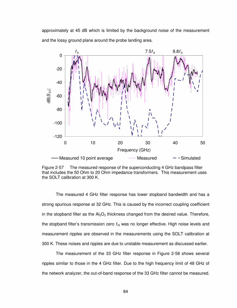
84
approximately at 45 dB which is limited by the background noise of the measurement
and the lossy ground plane around the probe landing area.
-120
-100
-80
-60
-40
-20
0
0 10 20 30 40 50
Frequency (GHz)
dB
|S2
1|
Measured 10 point average Measured Simulated
f 0 7.5f 0 9.8f 0
Figure 2-57 The measured response of the superconducting 4 GHz bandpass filter that includes the 50 Ohm to 20 Ohm impedance transformers. This measurement uses the SOLT calibration at 300 K.
The measured 4 GHz filter response has lower stopband bandwidth and has a
strong spurious response at 32 GHz. This is caused by the incorrect coupling coefficient
in the stopband filter as the Al2O3 thickness changed from the desired value. Therefore,
the stopband filter’s transmission zero fn3 was no longer effective. High noise levels and
measurement ripples are observed in the measurements using the SOLT calibration at
300 K. These noises and ripples are due to unstable measurement as discussed earlier.
The measurement of the 33 GHz filter response in Figure 2-58 shows several
ripples similar to those in the 4 GHz filter. Due to the high frequency limit of 48 GHz of
the network analyzer, the out-of-band response of the 33 GHz filter cannot be measured.

85
The in-band insertion loss is caused by measurement errors, poor contact on Nb lines
and loss in Nb lines as they do not become superconducting completely due to high
temperature at the probe contact.
-90
-80
-70
-60
-50
-40
-30
-20
-10
0
0 10 20 30 40 50
Frequency (GHz)
dB
|S21
|
Measured Simulated 10 point average
f 0
Figure 2-58 The measured response of the superconducting 33 GHz bandpass filter that includes the 50 Ohm to 20 Ohm impedance transformers. This measurement uses the SOLT calibration at 300 K.
2.12.6 The Filter’s Performance in Detector Systems
To test the filter’s isolation in the presence of interference in the actual
environment, the simulated 33 GHz filter’s response is rescaled to operate at the center
frequency of 100 GHz. Microwave energy from the sky, as shown in Figure 2-59, is
applied to the filter with the presence of 30 K far-infrared black body radiation from 300
to 600 GHz. The integral power from the filter is measured.
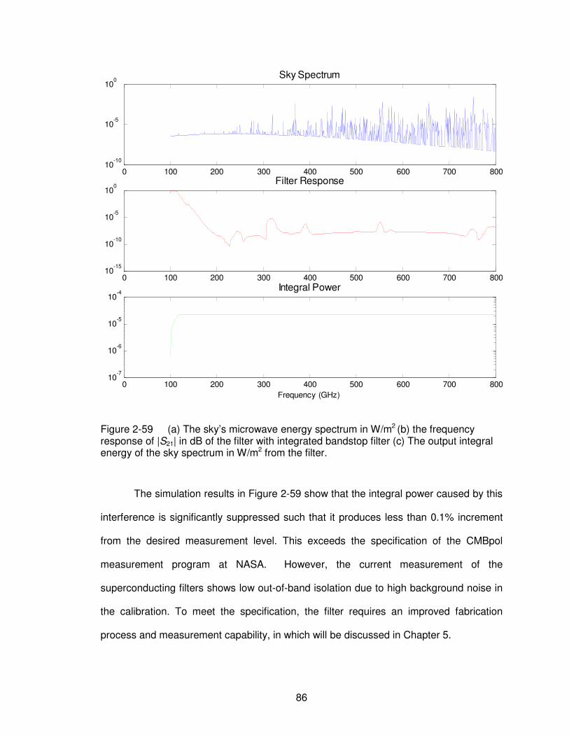
86
0 100 200 300 400 500 600 700 80010
-10
10-5
100
Sky Spectrum
0 100 200 300 400 500 600 700 80010
-15
10-10
10-5
100
Filter Response
0 100 200 300 400 500 600 700 80010
-7
10-6
10-5
10-4
Integral Power
Frequency (GHz)
Figure 2-59 (a) The sky’s microwave energy spectrum in W/m2 (b) the frequency
response of |S21| in dB of the filter with integrated bandstop filter (c) The output integral energy of the sky spectrum in W/m2 from the filter.
The simulation results in Figure 2-59 show that the integral power caused by this
interference is significantly suppressed such that it produces less than 0.1% increment
from the desired measurement level. This exceeds the specification of the CMBpol
measurement program at NASA. However, the current measurement of the
superconducting filters shows low out-of-band isolation due to high background noise in
the calibration. To meet the specification, the filter requires an improved fabrication
process and measurement capability, in which will be discussed in Chapter 5.

87
CHAPTER 3
3 BROADBAND AND LOW-LOSS MAGIC-T DEVELOPMENT
3.1 Literature Review
A microwave hybrid is an important component in a microwave system and has
been a subject of interest for several decades. In a radiometer system, the microwave
hybrid is used as one of the front-end components to extract the stroke parameters
(Skou, Laursen et al. 1999) in microwave signals. This dissertation focuses on the
design of the passive broadband 180º hybrid on the thin-film substrate that has low in-
band losss, broadband response and high sum-to-difference port isolation. The
operating frequency is in the Ka-Band (From 26 GHz to 40 GHz) or higher. The origin
and history of the broadband hybrid are addressed. Then, several approaches are
studied.
The 180º hybrid can be implemented using passive and active components. In
this proposal, the 180º hybrid is referred to as “hybrid” hereafter. Although active hybrids
(Tokumitsu, Hara et al. 1989) are significantly smaller than passive hybrids, they are not
used in passive radiometer applications. Since the active hybrids are made from
transistors, they have limited operating power. The hybrids’ transistor noise is also
added to the output signal. Moreover, the output responses are not as linear as those in
passive hybrids.
The literature review begins with the simplest passive hybrid design is called the
retrace hybrid. (Reed and Wheeler 1956). Most research focuses on reducing the size of
rat-race hybrids (Hirota, Minakawa et al. 1990; Kamitsuna 1992; Eccleston and Ong
2003; Chen and Tzuang 2004; Ghali and Moselhy 2004; Hettak, Morin et al. 2004; Ng,
Chongcheawchamnan et al. 2004; Okabe, Caloz et al. 2004; Sung, Ahn et al. 2004; Yun

88
2004). Among the research are studies related to reducing the physical length of the T-
line while maintaining the same electrical length (Eccleston and Ong 2003; Chen and
Tzuang 2004; Sung, Ahn et al. 2004; Yun 2004). The T-line with the defected ground
structure (DGS) is used in (Sung, Ahn et al. 2004; Yun 2004). The DGS in (Sung, Ahn et
al. 2004) also produces signal suppression out-of-band of interest. The hybrid size can
be reduced by 32 to 46 percent using artificial T-lines (Eccleston and Ong 2003), which
consist of shunt and series T-line stubs connected in series. Lumped capacitors can also
be incorporated in a T-line (Hirota, Minakawa et al. 1990; Kamitsuna 1992; Hettak, Morin
et al. 2004; Ng, Chongcheawchamnan et al. 2004). Using this technique, a 02Z λ/4 line
can be replaced by the 2Z0 T-line with λ/8 long and lumped capacitors at both ends of
the T-line (Kamitsuna 1992). The meandering lines can also be used to reduce the
overall size (Chen and Tzuang 2004; Ghali and Moselhy 2004). The techniques
described above do not give broadband response. Their bandwidth is equivalent to the
conventional retrace hybrid. Because of the discontinuities added to the hybrid, such as
multiple-bends, narrow T-line and DGS, these hybrids produce higher in-band insertion
loss than that of the conventional hybrid.
To improve the bandwidth and in-band return loss of the retrace hybrid, stepped-
impedance transformers are used (Kim and Naito 1982; Mgombelo 1989; Ahn and Wolff
2001). The values of the stepped-impedance transmission line are determined using
optimization techniques. Moreover, extra shunt T-line sections can be introduced to
improve the phase balance and increase passband bandwidth (Piernas, Hayashi et al.
2000).
Most research, which focuses on producing broad-brand response hybrids,
incorporates broadband 180º phase shifters in the hybrids. Broadband phase shifters
can be produced using left-handed T-lines (Okabe, Caloz et al. 2004). However, using

89
today’s technology these T-lines are in the form of distributed lumped elements.
Therefore, the left-handed T-line has limited use at the millimeter or sub-millimeter
frequency. Other techniques are related to the transition between TEM line and slotline.
Moreover, the 180º phase shifters can be in the form of coupled lines (Rehnmark 1977)
and balun structure (Jones 1960; Laughlin 1976; Ang and Leong 2002).
Broadband 180º phase shifters using co-planar waveguides (CPW) to slotlines
(SL) transition are widely used, since both CPW and SL are on the same layer, which
are simple to fabricate. The hybrids using this technique provide broadband response
and are more compact than the conventional retrace hybrid (Hirota, Tarusawa et al.
1987; Ho, Fan et al. 1994; Murgulescu, Moisan et al. 1994; Fan, Ho et al. 1995; Fan,
Kanamaluru et al. 1995; Fan, Heimer et al. 1997; Chang, Yang et al. 1999; Wang 1999).
Moreover, the length of each T-line section of these hybrids can be reduced to less than
λ/4 long (Murgulescu, Moisan et al. 1994; Fan, Ho et al. 1995). The magnitude and
phase imbalances of these hybrids are minimal and have the 3 dB bandwidth of more
than one octave. Despite their good performance, these hybrids are expensive to
fabricate since they require bondwires or airbridges to connect between two ground
planes of the CPW stripes. The airbridges/bondwires need to be placed at the locations
that have discontinuity and where long CPW lines are used. This placement reduces the
production yield of the hybrid. Moreover, at sub-millimeter wave frequencies, resulting
parasitics due to bondwires/ airbridges becomes so significant that they introduce phase
and amplitude imbalances in the upper operating frequency of the hybrid.
To eliminate the use of bondwires/airbridges in a hybrid design, MS-to-SL
transition technique is implemented (Ronde; Aikawa and Ogawa 1980; Ogawa, Hirota et
al. 1985; Hiraoka, Tokumitsu et al. 1989; Kim and Park 2002). The designs using this
technique produce a broadband response and can also be very compact (Hiraoka,
Tokumitsu et al. 1989). However, three of the ports are SL and require transition to the

90
MS line layer. Moreover, the sum and difference ports of the magic-T can be located on
the opposite side of the input ports (Aikawa and Ogawa 1980). This technique requires
that most T-lines in the structure be slot lines; therefore, the hybrid using this technique
has high slotline radiation. De Ronde proposed a very compact magic-T structure
(Ronde). However, no analytical design is determined. Since a large circular slot is
directly placed under the MS line in the structure, it produces high radiation loss if
operated at high frequency. Other types of hybrids are asymmetric coupled-transmission
lines (Carpenter; Gruszczynski; Kraker 1964; Nakajima and Tanabe 1996). Using this
technique requires two broadside coupled lines. Therefore, the hybrid requires two
metallization layers in addition to a ground plane layer. Although broadband response is
achieved, this hybrid produces high in-band phase and magnitude ripple.
3.2 Microstrip-to-slotline Transitions Using Slotline Stepped Circular
Ring
Microstrip-to-slotline (MS-to-SL) transitions (Knorr 1974) find use in a variety of
microwave applications. Many techniques have been developed to extend the transition
bandwidth using different types of terminations such as parallel sections of λ/4 stubs
(Akhavan and Mirshekar-Syahkal 1996) or lumped element terminations , or using the
impedance transformation techniques at the termination (Zhang, Wang et al. 2004).
Although transitions using these techniques have broadband characteristics, their
insertion loss typically increases gradually as frequency increases. This is partly due to
slotline radiation loss and the change in slotline impedance with frequency.
For the MS-to-SL transition (see Figure 3-6(a)) to effectively transfer power, the
microstrip requires a grounded-end termination, whereas the slotline requires an
opened-end termination at the transition. The effective lengths of the line used to

91
produce a grounded-end/opened-end termination determine the transition bandwidth. In
the lower transition frequency limit, the perimeter of the slotline “open” is small compared
to the guided wavelength, the termination will be effectively grounded. In the upper
transition frequency limit, as the perimeter approaches the scale of the wavelength, the
slotline termination acts as an unintended resonant ring-slot antenna. Similar
considerations apply to the complementary microstrip structure’s limitations; however, as
a practical matter, due to microstrip lines greater field confinement, radiation losses are
a lesser concern.
In order to reduce radiation loss in the MS-to-SL transition, this disseration
propose the use of slotline stepped impedance circular ring (SCR) termination. The
circuit model and radiation loss characteristics are studied. Three MS-to-SL transitions
are constructed using three SCR terminations that have different physical dimensions.
Two-port measurements are performed in the band of interest from 2 to 26 GHz. Finally,
the performance of the transition using the SCR termination is compared with the
transitions using slotline circular rings, circular pads and radial pads.
3.2.1 Slotline Stepped Circular Ring Termination
To suppress radiation, the electrical length of the slotline structure must be small
relative to the guided wave length over the operating frequency band (Stutzman and
Thiele 1998). From this perspective, the slotline SCR shown in Figure 3-1(a) has several
advantages over λ/4-long slotline terminations such as radial or circular stubs. The
slotline SCR is smaller in size, provides broadband response and reduces radiation loss

92
Figure 3-1 (a) The proposed slotline SCR (b) electric fields in the slotline SCR (arrow line). (c) the equivalent transmission-line circuit model of the slotline SCR. Grey areas represent ground plane.
The slotline SCR consists of three slotline sections with the characteristic
admittances of Y0, Y1 and Y2. Their physical lengths are l0, l1 and l2 and their electrical
lengths are φ, θ1 and θ2, respectively. By symmetry, the circular structure forces the
electric field (E-field) to cancel at center, creating low-loss virtual ground as shown in
Figure 3-1(b) over the operating band. Its equivalent circuit is shown in Figure 3-1(c).
When φ=0, the slotline section Y0 is discarded and the input admittance of the
termination can be expressed as:
( ) ( )( ) ( )22
212
tantan
tantan
2 θθ
θθ
R
RjYYin
+
−−= (3-1)
where R is the stepped admittance ratio Y1/Y2. In practice, the slotline admittance values
(Y1 and Y2) contain much smaller imaginary parts relative to their real parts. Thus, their
imaginary parts are negligible in the circuit analysis. At the center of the operating
frequency (f0), i.e., Yin=0 in (1), we obtain the relationship:
( ) ( )21 tantan θθ=R (3-2)

93
for a lossless structure. In practical implementation, the slotline SCR is designed at the
frequency above f0 and transformed to f0 using Y0 and a non-zero φ value. When the
non-zero φ value is used, we achieve a smaller SCR area with slightly narrower
operating bandwidth. The circuit model and the electro-magnetic (EM) simulation of the
slotline SCR are in agreement over a broad frequency range as shown in Figure 3-2.
The deviations from the model are mainly due to the SCR’s admittance stepped
discontinuities and the slotline’s characteristic impedance that changes with frequency.
0.00001
0.0001
0.001
0.01
0.1
1
10
0 5 10 15 20 25 30 35 40
Frequency (GHz)
|Yin| (S
iem
ens)
EM Simulation
mag(Y44)
Series3
EM Simulation, φ =8°
Circuit model, φ =0°
Circuit model, φ =8°
Figure 3-2 The input admittance of the SCR on the 0.102 mm-thick Rogers liquid crystal polymer (LCP) substrate using the EM simulation with the lossless transmission
line model (Y1= 6.8⋅10-3-j1.25⋅10-4 Siemens, Y0=Y2=1.1⋅10-2-j1.23⋅10-4 Siemens, θ1=26.0°
and θ2=29.7° at 10 GHz). φ values are at 10 GHz.
3.2.2 Reducing Radiation Loss with the Slotline SCR
To study radiation loss in a slotline SCR, the following loss factors are defined as
L1-port=1-|S11|2 and L2-port=1-|S11|
2-|S21|2. These equations are for a one-port slotline
termination and a back-to-back MS-to-SL transition, respectively, where S11 and S21 are

94
the reflection and transmission coefficients of the slotline structure, respectively. The
back-to-back MS-to-SL transition’s ports can be interchanged (i.e. S11=S22 and S21=S12).
If a lossless conductor and a loss-less substrate are used, L1-port and L2-port represent
radiation losses. The EM simulations of the L1-port of a slotline termination using Ansoft
Designer in Figure 3-3 show that the maximum L1-port value occurs at fr1 when Yin is
equivalent to the magnitude of the slotline’s port admittance Ys. This also occurs around
the frequency where Yin reaches the maximum value at fr2.
0.0001
0.001
0.01
0.1
1
0 10 20 30 40
|Yin
| (S
iem
en
s)
0
0.2
0.4
0.6
0.8
1
0 10 20 30 40
Frequency (GHz)
L1-p
ort
(%
)
Ys=0.05
Ys=0.02
Ys=0.01
Figure 3-3 Simulated L1-port of the slotline SCR in Figure 3-2 connected to a slotline with the characteristic impedance of Ys=0.01, 0.02 and 0.05 Siemens.

95
Moreover, radiation loss is reduced as the port admittance increases. Therefore,
to increase the low-radiation loss bandwidth, a high Ys value is used and the separation
between fr1 and fr2 must be maximized. This can be achieved by reducing the effective
total length of the slotline SCR while maintaining low Yin around the operating frequency.
From (3-2), a low R value is used, such that θ1 and θ2 are minimized. Moreover, the
condition θ1=2θ2 is used to extend fr2 away from f0 (Kuo and Shih 2003). For the layout
simplicity, this condition is approximated by l1=2l2. The simulation results in Figure 3-4
show that the radiation loss is reduced when the slotline length ratio of l1/l2 changes from
1 to 2 (in Type-I and Type-II terminations) and when R is decreased from 0.645 to 0.556
(in Type-II and Type-III terminations).
0
0.2
0.4
0.6
0.8
1
0 10 20 30 40 50
Frequency (GHz)
L1- P
ort
(-)
0.000001
0.00001
0.0001
0.001
0.01
0.1
|Yin
| (s
iem
en
)
Type-I Type-II Type-III
Figure 3-4 Simulated input admittance and L1-port of the slotline SCRs.
Type-I: R=0.645, W1=219 µm and l1=l2=2.03 mm.
Type-II: R=0.645, W1=219 µm and l1=2l2= 1.37 mm.
Type-III: R=0.556, W1=500 µm and l1=2l2=1.04 mm.
For all SCR types, l0=0.45mm, W0=W2=102µm and Ys=0.02 Siemens.

96
The radiation loss of the slotline SCRs can also be visualized from the perception
of E-field confinement around the termination. Using Ansoft HFSS software, the
simulated E-field in Figure 3-5 shows that the slotline circular ring provides the least
confinement while the SCR Type-III has the highest confinement. Therefore, the slotline
SCR Type-III provides the minimum radiation loss among the three.
Figure 3-5 The simulated E-Field magnitude at f0=10 GHz and at 19 GHz of the slotline terminations (a) circular ring, (b) SCR Type-I (c) SCR Type-II and (d) SCR Type-III. Slot areas are shown in white.
3.2.3 Hardware Implementation of Slotline SCRs in MS-to-SL Transitions
MS-to-SL transitions are fabricated on a 102µm-thick LCP substrate. Their center
frequency is at 10 GHz. The footprints of the transition with three different slotline SCR
terminations are shown in Figure 3-6. The photograph of the test structure is shown in
Figure 3-7(a) and (b).

97
Port 2:50 input
(a)
(b)
(c)
Slotline
Microstrip line
Wm1
Wm2
Lm1Lm2
Lm0
Wm0L
s1
Calibrated
reference plane
Ys
Port 1:50 input
Figure 3-6 The layout of back-to-back MS-to-SL transitions using the slotline SCR
terminations (a) Type-I, (b) Type-II (c) and Type-III. W1=W0=100 µm and Ls1=1.78 mm on all types above. Type-I, Type-II and Type-III have the same microstrip line dimensions.
(a) (b)
Figure 3-7 The photograph of the (a) top view and (b) bottom view of the seven MS-to-SL transitions and calibration lines on 0.102 mm-thick Roger’s LCP substrate. The
sample’s overall dimension is 86 mm × 70 mm.
The LCP substrate has the relative dielectric constant of 2.9. The microstrip line
sections in these transitions are terminated with stepped impedance stubs that have
dimensions: Wm1=0.34 mm, Wm2=0.85 mm and Lm1=1.25 mm. At input ports, the
microstrip line with the characteristic impedance of 50 Ohm is transformed to the Ys

98
value of 0.011 Siemens using a λ/4-long line (Lm0=4.86 mm). This Ys value is set by the
minimum slotline width allowed in our fabrication process. Transitions are connected to
SMA connectors and the Thru-Reflect-Line (TRL) calibration is used. The measured
minimum frequency is limited by the TRL calibration standards while the measured
maximum frequency is limited by the SMA connector’s operating frequency. For the
measurements, cavity resonances between the test fixture and instrument ground were
damped by placing the transitions 5mm above a 0.76 mm-thick ECCOSORB GDS sheet
(ECCOSORB 2006).
The MS-to-SL transition loss is calculated based on L2-port which includes the loss
from conductor and dielectric. By comparing the total loss of the MS-to-SL transition
using the circular pad, radial pad or circular ring terminations, the experimental results in
Figure 3-8 show that the transition using the slotline SCR produces the lowest in-band
insertion loss. At 12 GHz, the insertion loss of the transition using Type-III SCRs is 0.57
dB compared with 0.82 dB of the transition using radial stubs. Strong radiation can be
observed in the MS-to-SL transition using circular rings at 21 GHz as the terminations
become effective slotline antennas as shown in the L2-port plot in Figure 3-8.
Among the three SCR designs, the Type-III transition in Figure 3-9 has the least
pass-band radiation loss and is in the acceptable agreement with the one-port simulation
results. The fr1 and fr2 of the Type-III slotline SCR termination are approximately at 3 GHz
and 25 GHz, respectively.

99
Figure 3-8 Measured frequency responses of (a) dB|S21| and (b) the L2-port of the MS-
to-SL transitions with the slotline circular pad, circular ring, 50° radial pad, or Type-I SCR terminations.

100
0
0.1
0.2
0.3
0.4
0.5
0.6
2 4 6 8 10 12 14 16 18 20 22 24 26
Frequency (GHz)
L2-p
ort
=
1-|S
11|2
-|S
21|2
Figure 3-9 Measured frequency responses of the L2-port of MS-to-SL transitions Type-I, Type-II and Type-III.
3.3 A Low-loss Planar Magic-T using Microstrip-to-slotline Transition
A magic-T is one type of four-port microwave junction. In the ideal case it is
lossless and has a port sum (H) and port difference (E) which allow incident signals to
be divided or combined with a well defined relative phase. The structure approximating
these ideal properties has been widely used as a circuit element in correlation receivers,
frequency discriminators, balanced mixers, four-port circulators, microwave impedance
bridges, reflectometers, etc (Montgomery, Dicke et al. 1948).
To achieve the magic-T with desirable properties over a broad-band, both phase
and amplitude from two input ports must be identical as they are combined in-phase and
out-of-phase at port H and port E, respectively. Choosing the proper magic-T’s
electromagnetic topology with the correct symmetry is important and helps achieve the
desirable isolation and bandwidth.

101
The symmetry in the in-phase combining section can be achieved using
microstrip line (MS) (Ang and Leong 2002) or co-planar wave guide (CPW) (Fan, Ho et
al. 1995), whereas the symmetry in the out-of-phase combining section can be achieved
using sloltine (SL) (Kim and Park 2002), (Aikawa and Ogawa 1980). MS-to-SL or CPW-
to-SL transitions are necessary to connect between the in-phase and out-of-phase
combiners and to bring all ports to the same metal layer (Knorr 1974).
Several techniques were developed to effectively implement MS-to-SL or CPW-
to-SL transitions in magic-Ts. These techniques provide magic-Ts with broadband
response. Although the theoretical E-H port isolation of these magic-Ts is infinite, the
practical isolation level of these designs is typically limited to 35dB by the following
physical factors.
Firstly, it is limited by the magic-T layout asymmetry such as in (Fan, Ho et al.
1995) and errors from fabrication process as they produce unequal parasitic couplings
between port 1 and port 2. Secondly, it is limited by the transmission line dispersion as
the transmission line impedances in magic-T change with frequency (Gupta, Gang et al.
1996). This dispersion occurs more noticeable in a wide slotline and in a wide CPW than
in a microstrip line. Moreover, the magic-T using the CPW-to-SL transition also has an
additional isolation limit due to bondwires or airbridges parasitic and their slight
misplacement on the transmission line discontinuities in the structure. Finally, the
isolation is limited by electric-field (E-field) confinement and loss on the ground plane.
The magic-Ts using the transmission line mode conversion with a large slot area on
ground plane (Kim and Park 2002), (Aikawa and Ogawa 1980) have a limited E-H port
isolation as the high level of E-field coupling occurs directly between port E and port H.

102
3.3.1 Circuit Configuration
The proposed magic-T is shown in Figure 3-10. The in-phase combiner in Figure
3-10(a) consists of two quarter-wavelength (λ/4) microstrip lines, with the characteristic
impedance of Z1, combined at the H port. The out-of-phase combiner in Figure 3-10(b)
consists of two (λ/4) microstrip lines with the characteristic impedance of Z2 combined
with the half-wavelength (λ/2) line with the characteristic impedance of Z3. The out-of-
phase combined signal can be obtained from the slotline with the characteristic
impedance of Zsl at the center of the structure below the Z3 line. Finally, the slotline
section is transformed to the microstrip line output at port E.
Port 1 Port 2
Port H
Port E
Microstrip Line Slot Line
Z1
Z0
Z0
Z1
Z0
Zsl
Z3
Z2
Z2
Z0
Zs1
Zs2
(a)
(b)Lsl
y
x
Figure 3-10 The proposed broadband magic-T consisting of (a) the in-phase combiner and (b) the out-of-phase combiner using microstrip-to-slotline transition.

103
The proposed magic-T has several advantages over conventional magic-Ts as
follows. It requires only one short section of the MS-to-SL transition to achieve a
broadband 180 degree phase shift and an out-of-phase power combiner. Secondly, the
structure has a small total slotline area, thus minimizing radiation loss and parasitic
coupling to microstrip lines. The magic-T layout is also symmetric along the y-axis up to
port E at Zsl. As a result, the parasitic coupling from slotline sections to microstrip line
sections at port 1 and port 2 are equal. Thus, the E-H port isolation of the magic-T
exhibits broad-band characteristics. Moreover, it does not require via holes, bondwires
or airbridges which increase fabrication complexity and allow broadband operation in
mm-wave frequency. The magic-T is analyzed in odd and even modes up to the slotline
Zsl section as shown in Figure 3-11(a) and (b) respectively.
Figure 3-11 The (a) odd-mode and (b) even-mode electric field and the current flow in the proposed magic-T and in the microstrip and slotline junction at A-B.

104
In the odd mode, the signals from port 1 and port 2 are out-of-phase. This
creates a microstrip virtual ground plane along the y-axis of the magic-T. The slotline
SCR termination connected to the slotline Zsl also allows the MS-to-SL mode conversion
to occurs as demonstrated by electric-field and current directions around the A-B cross
section as shown in Figure 3-11(a).
In the even mode, the signals from port 1 and port 2 are in phase, thus creating a
microstrip virtual open along the y-axis of the magic-T as shown in Figure 3-11(b).
Electric-fields in the slotline at the A-B cross section are canceled thus creating a slotline
virtual short that prevents the signal flow to or from port E.
3.3.2 Magic-T Port Impedance Matching
The microstrip line section of the magic-T can be modeled as a half circuit for the
odd and even modes due to its symmetry along the y axis. By ignoring step impedance
discontinuities, these circuits are shown in Figure 3-11(a) and 3-10(b), respectively.
This model is valid at the center frequency (f0) and it approximates the hybrid’s
response around f0. The magnitude of the isolation between port 1 and port 2 and the
magnitude of input return loss at port 1 and port 2 are computed as follows
Isolation
Γ−Γ−=
−+++
2log20 (3-3)
Returnloss
Γ+Γ−=
−+++
2log20 (3-4)
where Γ+- and Γ++ are odd-mode and even-mode reflection coefficient at port 1 in Figure
3-12(a) and (b) respectively.

105
Zsl/2
Z0
Z1, λ/4
(a) (b)
Port 1
Z2, λ/4
Z3, λ/4
Zsl0/2, θ0
Zsl1
θ1Zsl2, , θ2
n : 1
Port E
2Z0
Open
Z0
Port 1
Z2, λ/4
Z3, λ/4
Z1, λ/4
Port H
Γ++
Γ+−
Figure 3-12 (a) The odd mode (b) The even mode equivalent half circuit model of the magic-T shown in Figure 3-11(a) and (b), respectively.
In the odd mode circuit shown in Figure 3-12(a), the port H becomes a virtual
ground. Using a λ/4 transformation through Z1 line, the virtual ground becomes an open
at port 1. To match Z0 at port 1 with Zsl/2 at port E, port 1 impedance is transformed to
the slot line impedance of nt2Zsl/2 using a Z2 line, Z3 line and the transformer ratio nt. In
the single mode limit, nt is dependent of the substrate thickness, the transmission line
characteristic impedance and the MS-to-SL physical alignment (Kim and Park 1997).
The slotline SCR is connected to the Zsl section to create a virtual open termination and
enables the MS-to-SL mode conversion. The slotline SCR characteristic is described in
section B. The relationship of Z0, Z2, Z3 and Zsl can be determined at f0 as follows:
2
3
22
02
=
Z
ZZnZ sl
t (3-5)
It is desirable that nt2Zsl/2 equals to Z0 to eliminate the discontinuity of microstrip
lines (i.e. Z2=Z3=Z0). However, for some fabrication processes, the value Zsl is limited to
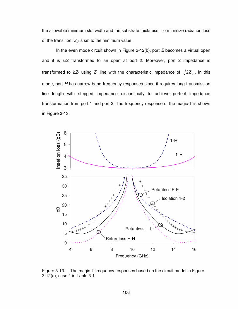
106
the allowable minimum slot width and the substrate thickness. To minimize radiation loss
of the transition, Zsl is set to the minimum value.
In the even mode circuit shown in Figure 3-12(b), port E becomes a virtual open
and it is λ/2 transformed to an open at port 2. Moreover, port 2 impedance is
transformed to 2Z0 using Z1 line with the characteristic impedance of 02Z . In this
mode, port H has narrow band frequency responses since it requires long transmission
line length with stepped impedance discontinuity to achieve perfect impedance
transformation from port 1 and port 2. The frequency response of the magic-T is shown
in Figure 3-13.
3
4
5
6
Inse
tio
n loss (
dB
)
1-E
1-H
0
5
10
15
20
25
30
35
4 6 8 10 12 14 16
Frequency (GHz)
dB
Returnloss H-H
Isolation 1-2
Retunloss 1-1
Retunloss E-E
Figure 3-13 The magic-T frequency responses based on the circuit model in Figure 3-12(a), case 1 in Table 3-1.

107
To increase the magic-T bandwidth at port H, the values Z1, Z2 and Z3 can be
numerically optimized as shown in case 2 in Table 3-1, for the magic-T on the 105 µm-
thick Roger’s liquid crystal polymer (LCP) substrate. The value of 94.1 Ohm is used for
Zsl. The frequency responses of the magic-T using the optimized parameters show an
improved bandwidth while producing small in-band ripples at the transmissions 1-H and
2-H as shown in Figure 3-14.
Table 3-1 Magic-T’s parameters used in Figure 3-12, the impedance unit is in Ohm
Magic-T section Case 1 Case 2
Microstrip line Z0=50, Z1=70.7, Z2=50, Z3=49 Z0=50, Z1=58.3, Z2=53.5, Z3=51.5
Slotline Zsl=94.1, nt=1, Zsl0=94.6, Zsl1=94.6, Zsl2=348.4, θ=17.3°, θ0=8.6°,
θ1=12.7°, θ2=24.9°
3
4
5
6
Insert
ion loss (
dB
)
1-E
1-H
0
5
10
15
20
25
30
35
4 6 8 10 12 14 16
Frequency (GHz)
dB
Returnloss H-H
Isolation 1-2
Retunloss 1-1
Retunloss E-E
Figure 3-14 The magic-T frequency responses based on the circuit model in Figure 3-12(b), case 2 in Table 3-1.
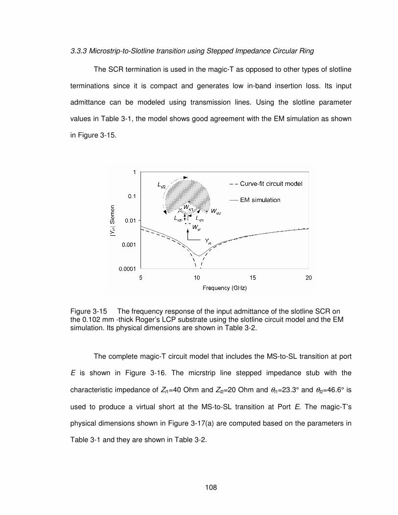
108
3.3.3 Microstrip-to-Slotline transition using Stepped Impedance Circular Ring
The SCR termination is used in the magic-T as opposed to other types of slotline
terminations since it is compact and generates low in-band insertion loss. Its input
admittance can be modeled using transmission lines. Using the slotline parameter
values in Table 3-1, the model shows good agreement with the EM simulation as shown
in Figure 3-15.
Figure 3-15 The frequency response of the input admittance of the slotline SCR on the 0.102 mm -thick Roger’s LCP substrate using the slotline circuit model and the EM simulation. Its physical dimensions are shown in Table 3-2.
The complete magic-T circuit model that includes the MS-to-SL transition at port
E is shown in Figure 3-16. The micrstrip line stepped impedance stub with the
characteristic impedance of Zt1=40 Ohm and Zt2=20 Ohm and θt1=23.3° and θt2=46.6° is
used to produce a virtual short at the MS-to-SL transition at Port E. The magic-T’s
physical dimensions shown in Figure 3-17(a) are computed based on the parameters in
Table 3-1 and they are shown in Table 3-2.

109
Port E
Port H Port 2
Port 1
Zsl/2 , θ
Zsl1
Z2
Z3
Z1
Z2
Z3
Z1
Zt, λ/4
Zt1
, θt1
Zt2
, θt2
Zsl2Z
sl0/2 Z
sl1Zsl2
λ/4λ/4λ/4 θ0
θ1
θ2
θ2
θ1
θ0
Zsl/2 , θ
n : 1Z
sl0/2
Z0
Z0Z
0
Z0
n : 1
Figure 3-16 The full circuit model of the proposed magic-T.
Figure 3-17 The layout and dimensions of the proposed magic-T on the Roger’s LCP substrate.
Table 3-2 The magic-T’s physical dimensions in millimeters.
Microstrip line sections Slotline sections W0=0.24, W1=0.19, W2=0.22,Wt=0.14, Wt1=0.34, Wt2=0.84, L1=4.76, L2=4.73,
L3=4.73, Lt=4.81, Lt1=1.25, Lt2=1.85
Wsl= Wsl1=0.10, Wsl2=1.83, Lsl=0.10, Lsl0=0.38, Lsl1=1.04, Lsl2=4.17

110
Two slotline half circuit sections are used in the magic-T model to preserve the
structure symmetry. The circuit model shows a very good agreement with the EM-
simulation as shown in Figure 3-18. The E-H isolation is infinite in the circuit model. The
1-E insertion loss has higher loss than that in the 1-H due to additional radiation loss
from the MS-to-SL transition at port E.
3.3.4 The Effect of Layout Asymmetry in Magic-T’s E-H Port Isolation
The isolation of the proposed magic-T is dependent on the phase and impedance
mismatch between port 1 and port 2 and the parasitic couplings between ports E and H.
The phase and impedance mismatch is caused by the fabrication misalignment
between microstrip and slotline, as well as asymmetric parasitic coupling from slotline to
micro-strip line in port 1 and port 2 around the out-of-phase combiner. Moreover, the
parasitic coupling is produced from the magic-T’s slotline section to microstrip line
sections at port H.
Although small fabrication misalignment can not be avoided, the E-H port
isolation can be improved by increasing the physical distance from port E to port H.
From Figure 3-19, the isolation is increased by more than 26 dB in the low frequency
side of f0 as the slotline length Lsl increases from 50 to 200 µm. However, small increase
in isolation is observed at the frequency above f0, since the parasitic coupling from port E
and H has more significant effect than the asymmetric parasitic coupling to port 1 and
port 2.

111
0
10
20
30
40
50
60
70
80
90
E-H
1-2
3
4
5
6
7
1-E
1-H
0
5
10
15
20
25
30
4 6 8 10 12 14 16
H-H
1-1
E-E
Figure 3-18 The frequency response of the magic-T using transmission model (dashed line) and using EM simulation (solid line).

112
0
20
40
60
80
100
4 8 12 16Frequency (GHz)
Isola
tion E
-H (
dB
)
Ls=20mil Ls=30mil Ls=40mil Ls=80milLsl=50 m L
sl=75 m L
sl=100 m L
sl=200 m
Figure 3-19 The simulated port E-H isolation of the magic-T with variable slotline length (Lsl).
3.3.5 Hardware Implementation of the Proposed Broadband Magic-T
The magic-T is designed on a 0.25mm-thick Duriod 6010 substrate. The design
is at 10 GHz and is based on the Duroid 6010 substrate as opposed to the LCP
substrate mentioned earlier since the fabrication using the LCP substrate is not
available. The circuit parameters and physical parameters of this magic-T are shown in
Table 3-3 and Table 3-4, respectively. The minimum slotline width used in the design is
0.1mm which is equivalent to the Zsl of 72.8 Ohm. The λ/4-long line with an impedance
value of Zt to used to transform Zsl to Z0 at port E. The photograph of the magic-T is
shown in Figure 3-20. The magic-T is calibrated using TRL method to de-embed
parasitic at the connectors and lines connected to the magic-T. The calibration reference
plane is shown in Figure 3-20(a).The TRL calibration standard on Duriod 6010 substrate
used in this measurement is shown in Figure 3-21.
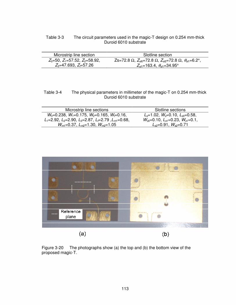
113
Table 3-3 The circuit parameters used in the magic-T design on 0.254 mm-thick Duroid 6010 substrate
Microstrip line section Slotline section
Z0=50, Z1=57.52, Z2=58.92, Z3=47.693, Zt=57.26
Zs=72.8 Ω, Zsl0=72.8 Ω, Zsl2=72.8 Ω, θsl1=6.2°,
Zsl1=163.4, θsl1=34.95°
Table 3-4 The physical parameters in millimeter of the magic-T on 0.254 mm-thick Duroid 6010 substrate
Microstrip line sections Slotline sections W0=0.238, W1=0.175, W2=0.165, Wt=0.16,
L1=2.92, L2=2.90, L3=2.87, Lt=2.79 ,Lm1=0.68, Wm1=0.37, Lm2=1.30, Wm2=1.05
Ls=1.02, Ws=0.10, Ls0=0.58, Ws0=0.10, Ls1=0.23, Ws1=0.1,
Ls2=0.91, Ws2=0.71
Figure 3-20 The photographs show (a) the top and (b) the bottom view of the proposed magic-T.

114
Figure 3-21 The photograph of the thru-reflect-line calibration standard used in the magic-T measurement.
The magic-T provides an average in-band insertion loss of 0.3 dB and 0.7 dB in
the in-phase and the out-of-phase power combining sections, respectively as shown in
Figure 3-22. The in-band frequency ranges from 6.6 GHz to 13.8 GHz, which is
equivalent to 72% bandwidth. The out-of-phase power combining section has higher
insertion loss than the in-phase combining section due to additional loss caused by
slotline radiation and microstrip line loss. Moreover, the magic-T has both low amplitude
and phase imbalance of less than 0.5 dB and 2 degree as shown in Figure 3-23 and
Figure 3-24, respectively. The return loss is greater than 10 dB in the operating
frequency bandwidth as shown in Figure 3-25 and Figure 3-26. The amplitude and
phase balance of the magic-T are computed as follows
Out-of-phase amplitude balance EE SS 21 −= (3-8a)
In-phase amplitude balance HH SS 21 −= (3-8b)
Out-of-phase amplitude balance EE SS 21 ∠−∠= (3-9a)
In-phase amplitude balance HH SS 21 ∠−∠= (3-9b)

115
, where S1E and S2E are forward transmission from port E to port 1 and from port E to
port 2, respectively. S1H and S2H are forward transmission from port H to port 1 and from
port E to port 2, respectively. The port 1-2 isolation is in good agreement with the
simulated results in Figure 3-27, however the minimum port E-H isolation is 32 dB, which
is 20 dB lower than predicted by the simulation due to infinite ground conductivity and
area.
0
5
10
15
20
25
30
35
40
45
2 4 6 8 10 12 14 16 18 20
Frequency (GHz)
Insert
ion loss (
dB
)
Measured 1-H Measured 1-E Measured 2-H Measured 2-E
Simulated 1-H Simulated 1-E Simulated 2-H Simulated 2-E
1-H, 2-H
1-E, 2-E
Figure 3-22 The magnitude of the in-phase and out-of-phase power dividing in dB of the magic-T. The referenced power dividing magnitude is 3 dB.

116
-15
-10
-5
0
5 6 7 8 9 10 11 12 13 14 15
Frequency (GHz)
Ph
ase b
ala
nce
(deg
ree)
-185
-180
-175
-170
Ou
t-of-
ph
ase b
ala
nce
(de
gre
e)
In-phase balance Out-of-phase balance
-0.8
-2.8
-180.2
-182.2
Figure 3-23 The measured frequency responses of the in-phase and out-of-phase phase balance of the magic-T.
-0.3
-0.2
-0.1
0
0.1
0.2
0.3
0.4
0.5
5 6 7 8 9 10 11 12 13 14 15
Frequency (GHz)
Am
plit
ud
e b
ala
nce
(d
B)
In-phase Out-of-phase
Figure 3-24 The measured frequency responses of the amplitude balance of the in-phase and out-of-phase power diving sections of the magic-T.

117
0
5
10
15
20
25
2 4 6 8 10 12 14 16 18 20
Frequency (GHz)
Retu
rnlo
ss (
dB
)
Measured E-E Measured H-H Simulated H-H Simulated E-E
H-H
E-E
Figure 3-25 The frequency response of the return loss of port E and port H of the magic-T.
0
5
10
15
20
25
30
35
2 4 6 8 10 12 14 16 18 20
Frequency (GHz)
Retu
rnlo
ss (
dB
)
Measured 1-1 Measured 2-2 Simulated 1-1 Simulated 2-2
Figure 3-26 The frequency response of the return loss of port 1 and port 2 of the magic-T.
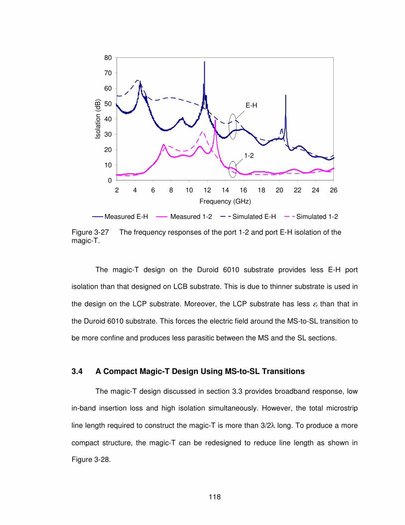
118
0
10
20
30
40
50
60
70
80
2 4 6 8 10 12 14 16 18 20 22 24 26
Frequency (GHz)
Isola
tion
(dB
)
Measured E-H Measured 1-2 Simulated E-H Simulated 1-2
E-H
1-2
Figure 3-27 The frequency responses of the port 1-2 and port E-H isolation of the magic-T.
The magic-T design on the Duroid 6010 substrate provides less E-H port
isolation than that designed on LCB substrate. This is due to thinner substrate is used in
the design on the LCP substrate. Moreover, the LCP substrate has less εr than that in
the Duroid 6010 substrate. This forces the electric field around the MS-to-SL transition to
be more confine and produces less parasitic between the MS and the SL sections.
3.4 A Compact Magic-T Design Using MS-to-SL Transitions
The magic-T design discussed in section 3.3 provides broadband response, low
in-band insertion loss and high isolation simultaneously. However, the total microstrip
line length required to construct the magic-T is more than 3/2λ long. To produce a more
compact structure, the magic-T can be redesigned to reduce line length as shown in
Figure 3-28.

119
Figure 3-28 The compact design of the magic-T using MS-to-SL transitions.
From Figure 3-28, the magic-T consists of five λ/4 microstrip lines with the
characteristic impedances of Z1, Z2 and Zt. It also consists of a slotline length Ls with the
slotline characteristic impedance of Zs. All ports are terminated with the microstrip lines
with the characteristic impedance of Z0. The slotline section is terminated with the
slotline SCR termination at both ends to provide broadband and low-loss MS-to-SL
transition and to allow out-of-phase combining to occur. Zt is used to transform slotline Zs
to the microstrip line Z0 at port E.
The design of the magic-T shown in Figure 3-28 uses similar concept to that
discussed in section 3.3. The signals from port 1 and port 2 are combined in phase at
the sum port and combined out-of-phase at the MS-to-SL transition along A-B as shown
in Figure 3-29(a) and (b), respectively.

120
Figure 3-29 (a) the odd-mode and (b) the even-mode electric field and the current flow in the compact magic-T.
3.4.1 Compact Magic-T’s Operation
In the odd mode, the signals from port 1 and port 2 are out-of-phase. This
creates a microstrip virtual ground plane along the y-axis of the magic-T. The slotline
SCR termination connected to the slotline Zsl also allows the MS-to-SL mode conversion
to occurs as demonstrated by electric-field and current directions around the A-B cross
section as shown in Figure 3-29(a).
In the even mode, the signals from port 1 and port 2 are in-phase, thus creating a
microstrip virtual open along the y-axis of the magic-T as shown in Figure 3-29(b).
Electric-fields in the slotline at the A-B cross section are canceled thus creating a slotline
virtual short that prevents the signal flow to or from port E.
3.4.2 Magic-T Port Impedance Matching
In order to match the impedance of all four ports of the magic-T. The magic-T is
analyzed in odd-mode and even-mode circuits up to Zs as shown in Figure 3-30.

121
Figure 3-30 (a) The odd-mode and (b) the even-mode equivalent circuit of the compact magic-T.
In the odd-mode, λ/4-line Z1 is used to transform the input characteristic
impedance Z0 at port 1 to the desired value of Zs/2. The value of Z1 can be derived as
follows:
0
2
12
ZZ
nZ s
t ⋅= (3-10)
where nt is the MS-to-SL transformer ratio. The λ/4-line Z2 is used to transform the
grounded-end to a virtual open at Zs. It is desirable that Z2 value is high relative to Zs to
create a broadband virtual open. The practical value of Z2 is set by the matching in the
even-mode analysis.
In the even-mode, the input impedance Z0 at port 1 is transformed to the in-
phase port impedance of 2Z0. Since the line Z1 is used to transform impedance Z0 to Zs/2
in odd-mode, the line Z2 must be used to transform the impedance Zs to 2Z0. Therefore,
Z2 can be computed as follows:

122
12
02 22
2 ZZ
nZZs
t =⋅= . (3-11)
The isolation and the return loss of port 1 and port 2 are derived in term of Γ++ and Γ+- as
in (3-3) and (3-4), respectively.
The magic-T is designed on a 10-mil thick Duroid 6010 substrate with the
dielectric constant of 10.2. The slotline is 0.1mm wide, which is the minimum width
allowable in this fabrication process. This corresponding Zs of 72.8 Ohm and all four
ports impedances are 50 Ohm. From (3-10) and (3-11) and nt =1, we obtain Z1 and Z2 of
42.7 Ohm and 60.33 Ohm, respectively. Using this circuit model, the frequency response
of the magic-T can be determined up to port E as show in Figure 3-31.
0
10
20
30
40
50
60
70
6 7 8 9 10 11 12 13 14
Frequency (GHz)
dB Return loss 1-1
Return loss H-H
Isolation 1-2
Return loss E-E
Figure 3-31 The frequency response of the magic-T using odd and even-mode half-circuit model.

123
The response shows that this magic-T provides broadband out-of-phase
combining response than the in-phase combining response. The in-phase combining
bandwidth is limited by two impedance transformation section in Z1 and Z2 used to
transform Z0 at port 1 to 2Z0 at port H in even mode. Moreover, the Z2 value needs to
satisfy the odd-mode match condition.
The slotline SCRs are used in this magic-T as terminations for the MS-to-SL
transition. The slotline SCR in this design is slightly more compact than that used earlier
by increasing the ratio ls1/ls2 from two to four. As a result, its loss is slightly reduced
compared with the previously proposed magic-T as shown in Figure 3-32.
1
10
100
1000
10000
100000
0 5 10 15 20 25 30 35 40
Frequency (GHz)
|Zin
|
0
0.1
0.2
0.3
0.4
0.5
0.6
1-|
S1
1|2
Port1Port1
Figure 3-32 The frequency response of the L1-port and the magnitude of the input impedance |Zin| of slotline SCR stubs with ls1/ls2=2 (solid line) and with ls1/ls2=4 (dashed line). Both of which have the same Ws0, Ls0 , Ws1 and Ws2 values provided in Table 3-6
This slotline SCR can be modeled using transmission lines as shown in section
3.2. Its equivalent circuit parameters and its physical parameters are provided in Table

124
3-5 and Table 3-6, respectively. The circuit model shows a good agreement with that
obtained from the method of moment simulation as shown in Figure 3-33.
Table 3-5 The compact magic-T circuit design parameters at 10 GHz
Microstrip line section Slotline section
Z1=42.7 Ω, Z2=60.33 Ω, Zt1=40 Ω
θt1=23.3°, θt2=46.6°, Zt2=20 Ω
Zs=72.8 Ω, Zsl0=72.8 Ω, Zsl2=72.8 Ω,
θsl0=13.57°, θsl2=6.2°, Zsl1=163.4 Ω,
θsl1=34.95°, θs=113.3°
Table 3-6 The physical parameters of the compact magic-T in millimeters.
Microstirp line section Slotline section L1=2.62, W1=0.26, L2=1.83, W2=0.14, Lt=2.80, Wt=0.16, Lt1=0.68, Wt1=0.37,
Lt2=1.30, Wt2=1.05
Ls=1.92, Ws=0.10, Ls0=0.58, Ws0=0.10, Ls1=0.23, Ws1=0.1, Ls2=0.91, Ws2=0.71
0.01
0.1
1
10
100
1000
2 4 6 8 10 12 14 16 18
Frequency (GHz)
|Zin
|
Circuit model
EM Simulation
Zin
Ls0
Ls1
Ls2 Ws1
Ws0
Ws0
Figure 3-33 The input impedance of the slotline SCR in the compact magic-T using the parameters provided in Table 3-5.
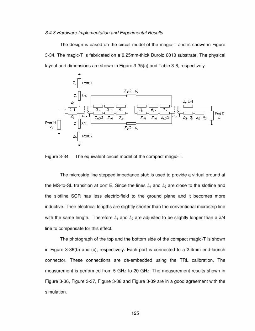
125
3.4.3 Hardware Implementation and Experimental Results
The design is based on the circuit model of the magic-T and is shown in Figure
3-34. The magic-T is fabricated on a 0.25mm-thick Duroid 6010 substrate. The physical
layout and dimensions are shown in Figure 3-35(a) and Table 3-6, respectively.
Figure 3-34 The equivalent circuit model of the compact magic-T.
The microstrip line stepped impedance stub is used to provide a virtual ground at
the MS-to-SL transition at port E. Since the lines L1 and L2 are close to the slotline and
the slotline SCR has less electric-field to the ground plane and it becomes more
inductive. Their electrical lengths are slightly shorter than the conventional microstrip line
with the same length. Therefore L1 and L2 are adjusted to be slightly longer than a λ/4
line to compensate for this effect.
The photograph of the top and the bottom side of the compact magic-T is shown
in Figure 3-36(b) and (c), respectively. Each port is connected to a 2.4mm end-launch
connector. These connections are de-embedded using the TRL calibration. The
measurement is performed from 5 GHz to 20 GHz. The measurement results shown in
Figure 3-36, Figure 3-37, Figure 3-38 and Figure 3-39 are in a good agreement with the
simulation.
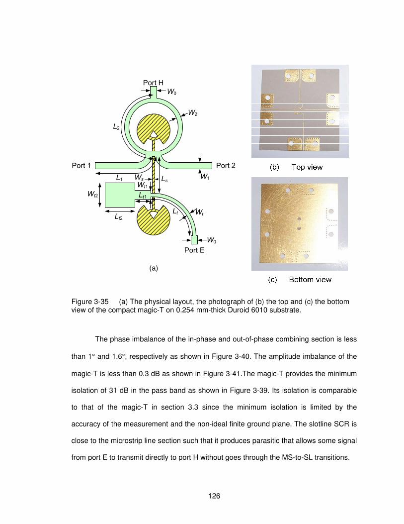
126
Port H
Port 1 Port 2
Port E
Ls
LtLt2
L1
L2
Wt2
Wt1
Wt
W1
W0
W0
W2
Ws
Lt1
(a)
Figure 3-35 (a) The physical layout, the photograph of (b) the top and (c) the bottom view of the compact magic-T on 0.254 mm-thick Duroid 6010 substrate.
The phase imbalance of the in-phase and out-of-phase combining section is less
than 1° and 1.6°, respectively as shown in Figure 3-40. The amplitude imbalance of the
magic-T is less than 0.3 dB as shown in Figure 3-41.The magic-T provides the minimum
isolation of 31 dB in the pass band as shown in Figure 3-39. Its isolation is comparable
to that of the magic-T in section 3.3 since the minimum isolation is limited by the
accuracy of the measurement and the non-ideal finite ground plane. The slotline SCR is
close to the microstrip line section such that it produces parasitic that allows some signal
from port E to transmit directly to port H without goes through the MS-to-SL transitions.

127
0
5
10
15
20
25
30
35
2 4 6 8 10 12 14 16 18 20
Frequency (GHz)
Inse
rtio
n lo
ss (
dB
)
Measured 2-E Measured 1-E Simulated 1-E Simulated 2-E
Measured 1-H Measured 2-H Simulated 1-H Simulated 2-H
1-E, 2-E
1-H, 2-H
Figure 3-36 The frequency response of the in-phase and the out-of-phase power dividing of the compact magic-T.
0
5
10
15
20
25
30
35
40
2 4 6 8 10 12 14 16 18 20
Frequency (GHz)
Retu
rnlo
ss (
dB
)
Measured E-E Measured H-H Simulated E-E Simulated H-H
H-H
E-E
Figure 3-37 The frequency response of the return loss at port E and port E of the compact magic-T.

128
0
5
10
15
20
25
30
35
40
2 4 6 8 10 12 14 16 18 20
Frequency (GHz)
Re
turn
loss (
dB
)
Measured 1-1 Measured 2-2 Simulated 2-2 Simulated 2-2
Figure 3-38 The frequency response of the return loss at port 1 and port 2 of the compact magic-T.
0
10
20
30
40
50
60
70
80
90
2 4 6 8 10 12 14 16 18 20 22 24 26
Frequency (GHz)
Isola
tion
(d
B)
E-H
1-2
Figure 3-39 The frequency response of measured (solid line) and simulated (dashed line) of port 1-2 and port E-H isolation of the compact magic-T.

129
-15
-10
-5
0
4 5 6 7 8 9 10 11 12 13 14 15 16
Frequency (GHz)
In-o
f-p
ha
se
ba
lan
ce
(d
eg
ree
)
-185
-180
-175
-170
Ou
t-o
f-p
ha
se
ba
lan
ce
(d
eg
ree
)
In-phase balance Out-of-phase balance
-0.6
-2.6
-183.2
-180
Figure 3-40 The frequency response of the in-phase and out-of-phase phase balances in degree of the compact magic-T.
-0.4
-0.3
-0.2
-0.1
0
0.1
0.2
0.3
0.4
5 6 7 8 9 10 11 12 13 14 15
Frequency (GHz)
Am
plit
ude
bala
nce (
dB
)
In-phase Out-of-phase
Figure 3-41 The frequency response of the in-phase and out-of-phase amplitude balances in dB of the compact magic-T.

130
The performance of the both broadband magic-T and compact magic-T can be
compared in the prior state-of-the-art planar magic-T designs as shown in Table 3-7.
Both broadband magic-T and compact magic-T have the lowest in-band insertion loss
and the highest E-H port isolation in the operating band compared with prior designs.
Moreover, the proposed magic-Ts have the lowest smallest phase imbalance in the
operating bandwidth with return loss of more than 12 dB.
Table 3-7 The comparison of the performance of the proposed magic-T among several magic-Ts that use slotline transitions in their operating bandwidth.
Magic-T designs
Center frequency
(GHz)
Insertion loss S1E, S2E (dB)
Phase balance S1E, S2E
Isolation Port 1-2
Isolation E-H
Broadband Magic-T
10 0.5 < ± 1° >15 > 30
Compact Magic-T
10 0.3 < ± 1.6° >20 > 30
(Hiraoka, Tokumitsu et
al. 1989)
10 0.9 n/a >14 > 27
(Ho, Fan et al. 1994)
3 1.2 < ± 1.5° >12 > 35
(Wang 1999) 2 0.8 < ± 5° >20 >20
(Fan, Heimer et al. 1997)
3 0.9 < ± 1.5° >16 >28
(Aikawa and Ogawa 1980)
6 0.9 < ± 2.1° >12 >30
(Kim and Park 2002)
2 1 < ± 2° >23 >30

131
CHAPTER 4
4 CONCLUSIONS
The dissertation presents the development of bandpass filters with high out-of-
band performance and loss-low magic-Ts. The conclusion consists of two sections: the
bandpass filter design and the magic-T design as follows.
In the bandpass filter research, developed are the techniques to produce the
compact bandpass filter with very high out-of-band attenuation and bandwidth with
minimal loss in the operating band.
New microstrip filter design techniques have been introduced. These techniques
are implemented in the filters with coupled resonators. They simplify and provide an
analytical guidance for the filter design with high out-of-band suppression. The double
split-end structure relaxes the coupling requirement between filter stages while providing
additional transmission zeros out-of-band. The Qsi of the minimum-size SIR is
analytically derived for the first time. The proposed techniques allow at least N+1
transmission zeros to exist in an Nth order filter design below the third lowest spurious
resonance frequency. Using these techniques, the filter can simultaneously produces
low in-band loss and wide stop-band bandwidth.
The SIR with the built-in internal coupler has been developed. It reduces the
number of λ/2 SIRs required by the filter design. This SIR increases the filter’s lowest
spurious resonance frequency to a higher frequency than the maximum limit of the
conventional λ/2 SIR. Only one metal patterned layer is required to construct the filter
using these SIRs.
The broadband bandstop filter has been introduced and integrated with the SIR
bandpass filter for the first time. Transmission poles and zeros of the bandstop filter

132
have been derived and properly allocated to suppress attenuation out-of-band and
minimize bandstop filter effect on the filter passband response. The response of this filter
shows a significant improvement in the out-of-band response.
In the magic-T research, several techniques are developed such that the magic-T
provides low loss and broadband responses. To design the magic-Ts, the minimum size
microstrip-to-slotline transition that has high layout symmetry between port 1 and port 2
is used. The magic-T using these techniques provides high E-H port isolation and has
low in-band insertion loss and has broadband responses. Moreover, it is simple to
fabricate since it requires only two metallized layers and requires no via holes.
Slotline stepped circular rings have been introduced and used in microstrip-to-
slotline transitions. The transitions using this technique provide low in-band insertion loss
and broadband response by eliminating gradual radiation loss close to in-band.
Moreover, the structure is more compact than the conventional slotline radial pad or
circular pad. The magic-T using the slotline SCR has an improved in-band response
over other prior known state-of-the-art planar magic-Ts.

133
CHAPTER 5
5 RECOMMENDATIONS
This dissertation introduces techniques used in filter and magic-T designs that
improve their performance over the existing state-of-the-art designs. The filter designed
using the techniques described in this dissertation is recommended for use in the
applications that require low in-band loss and very high out-of-band attenuation such as
in radio-astronomy. It can also be used in military systems where strong out-of-band
interference is presence. On the other hand, the magic-T designed using the techniques
described in this dissertation is recommended for use in the frequency multiplier systems
where the input and output signals must be isolated from local oscillators. In addition, it
can be used in microwave polarimeters.
As recommended future works, there are two possible ways to improve the
bandpass filters. Firstly, in the design perspective, the elliptic function can be used in the
filter’s passband response as opposed to conventional Butterworth or Chevychev
functions. Moreover, the bandpass filters can be constructed from a broadband
bandstop filter combined with a high-pass filter. The proper transmission pole locations
of both bandstop and high-pass filter must be determined such that a proper bandpass
filter response is achieved. The second improvement can be in the measurement and
fabrication since high noise level was observed when measured at 4.3K. The cryogenic
measurement can be improved by reducing the probe temperature and the vibration
from the vacuum pump line. To provide a reliable contact between the probe and the
substrate, thin layer of gold deposition can be added on the top of the Nb layer where
the measurement probes land on the sample. This protects the Nb line from oxidation
and guarantees a direct connection contact.

134
The recommended future development of the magic-T includes the improvement
in input isolation. In addition, possible is extending the techniques described in this
dissertation to be used in the quadrature hybrid to provide high input and output
isolation.

135
APPENDIX A: SUPERCONDUCTING MICROSTRIP LINE MODELING
The close form solution of the superconducting microstrip line characteristic
impedance and phase constant derived by G. Yassin and S. Withington are as follows.
By defining
1212 22 −+−= bxbbxp (A1)
htb /1+= (A2)
Where t is the thickness of the film and h is the thickness of the dielectric.
ra is given by
( ) ( )
−−
+−−−= −−
p
pp
p
p
h
wra
4
1lntanh
1
21ln 2/11
2/1
π
(A3)
Where w is the microstrip line width. rb is given by
rborb = (A4)
For w/h ≥ 5 and
( )( )[ ] ( )
( )2/1
2/1
12/1
2/1
12/1
21tanh2
1tanh11
ph
w
rbop
prbop
rbo
prbopprborborborb
π+
−
−−
−
−++−−−=
−
−
(A5)
Otherwise, where
∆+
+= ln2
1prbo η
(A6)
−
−+
++= −− 2/11
2/1
2/1 tanh21
4ln1
2
1
2p
pp
p
h
wp
πη .
(A7)
∆ equals to whichever is the largest of η and p.
The penetration factor (χ) is defined as follows

136
[ ]
[ ]
++++
<++++
=
otherwise./2ln2
2121
2//ln2
2121
rarb
IgIgIsIs
hwrarb
IgIgIsIs
π
π
χ (A8)
Where, for the bottom surface of the strip, we get
( ) ( )( )
−
++−=
1
212ln1
2/1
pra
pRarappIs
(A9)
( )( )rapraRa −−= 1 (A10)
For the top surface of the strip we get
( ) ( )( )
−
−++−−=
1
212ln2
2/1
prb
pRbrbppIs
(A11)
( )( )prbrbRb −−= 1 (A12)
And for the ground plane we have
( ) ( )( )
−
+++−=
1
'212ln1
2/1
prb
pRbrbppIg
(A13)
( )( )prbrbRb ++= 1' (A14)
( ) ( )( )
−
+++=
1
'212ln2
2/1
pra
pRarappIg
(A15)
( )( )praraRa ++= 1' (A16)
The fringing factor is defined as follows
=
ra
rb
w
hK f
2ln
2
π.
(A17)
The geometrical factor g1 is defined as follows
fwK
hg =1 .
(A18)
The propagation constant (β) and characteristic impedance (η) can be found as follows

137
2/1
21
+
=
hm
m λχ
η
β
η
β.
(A19)
Where
reffm ek0=β (A20)
reff
me
g10ηη = .
(A21)
The effective dielectric constant of the microstrip line is defined as follows
w
h
eee rr
reff
121
1
2
1
2
1
+
−+
+= .
(A22)
Close form sf1977olution of the characteristic impedance of the loss-less microstrip line
as in (Pozar 1997) are as follows
( )[ ]
>+++
<
+
=
.2for444.1ln667.0393.1
120
2for4
8ln
60
0
hwhwhwreff
hwh
w
w
h
reffZ
ε
πε
(A23)

138
REFERENCES
Ahn, H.-R. and I. Wolff (2001). "General design equations, small-sized impedance transformers,
and their application to small-sized three-port 3-dB power dividers." IEEE Trans. Microwave Theory Tech. 49(7): 1277-1288.
Aikawa, M. and H. Ogawa (1980). "A new MIC magic-T using coupled slot lines." IEEE Trans. Microwave Theory Tech. MTT-28(6): 523-528.
Akhavan, H. G. and D. Mirshekar-Syahkal (1996). "Analysis of broadband microstrip-slotline transitions with multi-arm stubs." Electronics Letters 32(23): 2106-2108.
Ang, K. S. and Y. C. Leong (2002). "Converting baluns into broad-band impedance-transforming 180° hybrids." IEEE Trans. Microwave Theory Tech. 50(8): 1990-1995.
Avrillon, S., I. Pele, et al. (2003). "Dual-band power divider based on semiloop stepped-impedance resonators." IEEE Trans. Microwave Theory Tech. 51(4): 1269-1273.
Banciu, M. G., A. Ioachim, et al. (2002). Miniature microstrip resonators and filters for GSM/GPRS. IEEE.
Banciu, M. G., R. Ramer, et al. (2003). "Compact microstrip resonators for 900 MHz frequency band." IEEE Microwave and Wireless Comp. Letters 13(5): 175-177.
Carpenter, E. W. "An asymmetric non-monotonic stripline magic-T." 320-323.
Chang, C.-Y., C.-C. Yang, et al. (1999). "A multioctave bandwidth rat-race singly balanced mixer." IEEE Microwave and Guided Wave Letters 9(1): 37-39.
Chang, K. F. and K. W. Tam (2005). "Miniaturized cross-coupled filter with second and third spurious response suppression." IEEE Microwave and Wireless Comp. Letters 15(2): 122-124.
Chen, C.-C. and C.-K. C. Tzuang (2004). "Synthetic quasi-TEM meandered transmission lines for compacted microwave integrated circuits." IEEE Trans. Microwave Theory Tech. 52(6): 1637-1647.
Eccleston, K. W. and S. H. M. Ong (2003). "Compact planar microstripline branch-line and rat-race couplers." IEEE Trans. Microwave Theory Tech. 51(10): 2119-2125.
ECCOSORB (2006). Emerson and Cumming microwave products www.eccosorb.com: Randolph, MA, 02368.
Fan, L., B. Heimer, et al. (1997). Uniplanar hybrid couplers using asymmetrical coplanar strip lines. IEEE Int. Microwave Symp.
Fan, L., C.-H. Ho, et al. (1995). "Wide-band reduced-size uniplanar magic-T, hybrid-ring, and de Ronde's CPW-slot couplers." IEEE Trans. Microwave Theory Tech. 43(12): 2749-2757.

139
Fan, L., S. Kanamaluru, et al. (1995). A new wide-band and reduced-size uniplanar magic-T.
IEEE Int. Microwave Symp.
Ghali, H. and T. A. Moselhy (2004). "Miniaturized fractal rat-race, branch-line and coupled-line hybrids." IEEE Trans. Microwave Theory Tech. 52(11): 2513-2519.
Gruszczynski, S. Wide band asymmetric coupled-transmission-line magic-T and sum-difference circuit. IEEE.
Gupta, K. C., R. Gang, et al. (1996). Microstrip lines and slotlines. Norwood, MA, Artech House.
Haig, D. (1998). A beginner's guide to the cosmic microwave background, http://www.mssl.ucl.ac.uk/www_astro/submm/CMBtutframe.html.
Hettak, K., G. A. Morin, et al. (2004). A novel compact multi-layer MMIC CPW branchline coupler using thin-film microstrip stub loading at 44GHz. IEEE Int. Microwave Symp.
Hiraoka, T., T. Tokumitsu, et al. (1989). "Very small wide-band MMIC magic T's using microstrip lines on a thin dielectric film." IEEE Trans. Microwave Theory Tech. 37(10): 1569-1575.
Hirota, T., A. Minakawa, et al. (1990). "Reduced-size branch-line and rat-race hybrids for uniplanar MMIC's." IEEE Trans. Microwave Theory Tech. 38(3): 270-275.
Hirota, T., Y. Tarusawa, et al. (1987). "Uniplanar MMIC hybrids - a proposed new MMIC structure." IEEE Trans. Microwave Theory Tech. MTT-35(6): 576-581.
Ho, C.-H., L. Fan, et al. (1994). "New uniplanar coplanar waveguide Hybrid-Ring Couplers and Magic-T's." IEEE Trans. Microwave Theory Tech. 42(12): 2440-2448.
Hong, J.-S. and M. J. Lancaster (1996). "Couplings of microstrip square open-loop resonators for cross-coupled planar microwave filters." IEEE Trans. Microwave Theory Tech. 44(12): 2099-2108.
Hsieh, M.-Y. and S.-M. Wang (2005). "Compact and Wideband Microstrip Bandstop Filter." IEEE Microwave and Wireless Comp. Letters 15(7): 472-474.
Ishizaki, T. and T. Uwano (1994). A stepped impedance comb-line filter fabricated by using ceramic lamination technique. IEEE Int. Microwave Symp.
Jones, E. M. T. (1960). "Wide-band strip-line magic-T." IRE Trans Microwave Theory Tech.: 160-168.
Kaddour, D., E. Pistono, et al. (2004). "Compact and selective lowpass filter with spurious suppression." Electronics Letters 40(21).
Kamitsuna, H. (1992). "A very small, low-loss MMIC rat-race hybrid using elevated coplanar waveguides." IEEE Microwave and Guided Wave Letters 2(8): 337-339.
Karacaoglu, U., I. D. Robertson, et al. (1994). An improved dual-mode microstrip ring resonator filter with simple geometry. Proc. 1994 European Microwave Conf., Cannes, France.

140
Kerr, A. R. (1999). "Surface impedance of superconductors and normal conductors in EM
simulators." NRAO Electronics Division Internal Report 302.
Kim, D. I. and Y. Naito (1982). "Broad-band design of improved hybrid-ring 3-dB directional couplers." IEEE Trans. Microwave Theory Tech. 30(11): 2040-2046.
Kim, J. P. and W. S. Park (1997). "Analysis of an inclined microstrip-slot-line transition with the use of the spectral-domain immittance approach." Microwave and Optical Technology Letters 15(4): 256-260.
Kim, J. P. and W. S. Park (2002). "Novel configurations of planar multilayer magic-T using microstrip-slotline transition." IEEE Trans. Microwave Theory Tech. 50(7): 1683-1688.
Kim, K., S. Kim, et al. (2004). "Compact microstrip lowpass filter using shunt open stubs and coupled slots on ground plane." Electronics Letters 40(5).
Knorr, J. B. (1974). "Slotline transitions." IEEE Trans. Microwave Theory Tech. MTT-22: 548-554.
Kraker, D. I. (1964). "Asymmetric coupled-transmission-line magic-T." IEEE Trans. Microwave Theory Tech.: 595-599.
Kuo, J.-T. and H.-S. Cheng (2004). "Design of quasi-elliptic function filters with a dual-passband response." IEEE Microwave and Wireless Comp. Letters 14(10): 472-474.
Kuo, J.-T. and E. Shih (2002). Stepped impedance resonator bandpass filters with tunable transmission zeros and its applications to wide stopband design. IEEE Int. Microwave Symp. , Seattle, Washington.
Kuo, J.-T. and E. Shih (2003). "Microstrip stepped impedance resonator bandpass filter with an extended optimal rejection bandwidth." IEEE Trans. Microwave Theory Tech. 51(50): 1554-1559.
Kuo, J., W. Hsieh, et al. (2004). Design of two-stage UIR and SIR bandpass filters with an elliptic function-like response. IEEE Int. Microwave Symp. , Forthworth, Texas.
Lancaster, M. J. (1977). Passive microwave device applications of high-temperaturs superconductors. Cambridge, Cambridge University Press.
Lancaster, M. J., F. Huang, et al. (1996). "Miniature superconducting filters." IEEE Microwave Theory Tech. 44(7): pp.1339-1346.
Laughlin, G. J. (1976). "A new impedance-matched wide-band balun and magic tee." IEEE Trans. Microwave Theory Tech. MTT-24(3): 135-141.
Lee, B. H., S. S. Park, et al. (2002). "Laminated bandpass filter using tapped resonators." Electronics Letters 38(23): 1452-1453.
Lee, M.-Q., K.-K. Ryu, et al. (2002). Novel low-pass filter for broad-band spurious suppresion. IEEE Int. Microwave Symp.: 1797-1800.

141
Liang, J.-F., C.-f. Shih, et al. (1999). HTS microstrip filters with mutiple symmetric and
asymmetric prescribed tranmission zeros. IEEE Int. Microwave Symp.
Lopetegi, T., M. A. G. Laso, et al. (2004). "Microstrip "wiggly-line" bandpass filters with multispurious rejection." IEEE Microwave and Wireless Comp. Letters 14(11): 531-533.
Makimoto, M. and S. Yamashita (1980). "Bandpass filters using parallel coupled stripline stepped impedance resonators." IEEE Trans. Microwave Theory Tech. MTT-28(12): 1413-1417.
Makimoto, M. and S. Yamashita (2001). Microwave resonators and filters for wireless communication : theory, design, and application, Springer.
Matsuo, M., H. Yabuki, et al. (2000). The design of a half-wavelength resonator BPF with attenuation poles at desired frequencies. IEEE MTT-S Int. Microwave Symp.
Matthaei, G. L., L. Young, et al. (1980). Microwave filters, impedance-matching networks, and coupling structures. Norwood, MA, Artech House.
Mgombelo, H. R. (1989). "New impedance transforming rat-race hybrid ring." Electronics Letters 26(13): 837-839.
Montgomery, C. G., R. H. Dicke, et al. (1948). Principles of microwave circuits.
Murgulescu, M.-H., E. Moisan, et al. (1994). "New wideband, 0.67λg circumference 180° hybrid ring coupler." Electronics Letters 30: 299-300.
Nakajima, M. and H. Tanabe (1996). A design technique for raising upper frequency limit of wide-band 1800 Hybrids. IEEE Int. Microwave Symp. .
Nam, H., H. Lee, et al. (2001). "A design and fabrication of bandpass filter using miniaturized microstrip square SIR." IEEE: 395-398.
NASA (2005). Wilkinson microwave anisotropy probe. http://map.gsfc.nasa.gov.
Ng, C. Y., M. Chongcheawchamnan, et al. (2004). Lumped-distributed hybrids in 3D-MMIC technology. IEEE Proc.-Microw. Antenna Propag.
Ogawa, H., T. Hirota, et al. (1985). "New MIC power dividers using coupled microstrip-slot lInes: two-sided MIC power dividers." IEEE Trans. Microwave Theory Tech. MTT-33(11): 1155-1164.
Okabe, H., C. Caloz, et al. (2004). "A compact enhanced-bandwidth hybrid ring using a artificial lumped-element left-handed transmission-line section." IEEE Trans. Microwave Theory Tech. 52(3): 798-804.
Padhi, S. K. and N. C. Karmakar (2004). "Spurious harmonics suppression of tapered SIR band-pass filter using electromagnetic bandgap (EBG) structure." IEEE: 3561-3564.

142
Pang, H.-K., K.-M. Ho, et al. (2004). A compact microstrip λ/4-SIR interdigital bandpass filter with extended stopband. IEEE Int. Microwave Symp., Forthworth, TX.
Piernas, B., H. Hayashi, et al. (2000). "Improvement of the design of 1800 rat-race hybrid." Electronics Letters 36(12): 1035-1036.
Pozar, D. M. (1997). Microwave engineering, Wiley.
Quendo, C., E. Rius, et al. (2001). "Integration of optimized low-pass filters in a bandpass filter for out-of-band improvement." IEEE Trans. Microwave Theory Tech. 49(12): 2376-2383.
Reed, J. and G. J. Wheeler (1956). "A method of analysis of symmetrical four-port networks." IRE Trans. Microwave Theory Tech.: 246-252.
Rehnmark, S. (1977). "Wide-band balanced line microwave hybrids." IEEE Trans. Microwave Theory Tech. MTT-25: 825-830.
Ronde, F. C. d. (1970). A new class of microstrip directional couplers. IEEE.
Sagawa, M., M. Makimoto, et al. (1997). "Geometrical structure and fundamental characteristics of microwave stepped-impedance resonators." IEEE Trans. Microwave Theory Tech. 45(7): 1078-1085.
Sagawa, M., M. Makimoto, et al. (1985). "A design method of bandpass filters using dielectric-filled coaxial resonators." IEEE Trans. Microwave Theory Tech. MTT-32(2): 152-157.
Sagawa, M., H. Shirai, et al. (1993). "Bandpass filters using microstrip linear tapered tranmission line resonators." IEICE Trans. Electron. E76-C(6): 985-991.
Sagawa, M., K. Takahashi, et al. (1989). "Miniaturized hairpin resonator filters and their application to receiver front-end MIC's." IEEE Trans. Microwave Theory Tech. 37(12): 1991-1997.
Sanada, A., H. Takehara, et al. (2002). λ/4 stepped-impedance resonator bandpass filters fabricated on coplanar waveguide. IEEE Int. Microwave Symp.
Skou, N., B. Laursen, et al. (1999). "Polarimetric radiometer configurations: potential accuracy and sensitivity." IEEE Trans. Geoscience Remote Sens. 37(5): 2165-2171.
Stracca, G. B. and A. Panzeri (1986). "Unloaded Q-factor of stepped-impedance resonators." IEEE Trans. Microwave Theory Tech. MTT-34(11): 1214-1219.
Stutzman, W. L. and G. A. Thiele (1998). Antenna Theory and Design. NY, John Wiley & Son, Inc.
Sung, Y. J., C. S. Ahn, et al. (2004). "Size reduction and harmonic suppression of rat-race hybrid coupler using defected ground structure." IEEE Microwave Wireless Comp. Letters 14(1): 7-9.
Swanson, D. (1989). Thin-film lumped-element microwave filters. IEEE Int. Microwave Symp.

143
Tokumitsu, T., S. Hara, et al. (1989). Very small, ultra-wideband MMIC magic-T and applications to combiners and dividers IEEE Int. Microwave Symp.
U-yen, K., W. J. Wollack, et al. (2004). The design of a compact, wide spurious-free bandwidth bandpass filter using stepped impedance resonators. IEEE European Microwave Conf., Paris, France.
Uchida, H., Y. Furukawa, et al. (2002). Low-Spurious coaxial-line bandpass filter with saucer-loaded stepped-impedance resonators. IEEE Int. Microwave Symp.
Wada, K. and I. Awai (1999). A λ/2 CPW resonator BPF with multiple attenuation poles and its miniaturization. IEEE Int. Microwave Symp.
Wang, H. and L. Zhu (2005). Microstrip bandpass filter with ultra-broad rejection band using stepped impedance resonator and high-impedance transformer. IEEE MTT-S Int. Microwave Symp. Dig., Longbeach, CA.
Wang, T. (1999). "Size-reduction and band-broadening design technique of uniplanar hybrid ring coupler using phase inverter for M(H)MIC's." IEEE Trans. Microwave Theory Tech. 47(2): 198-206.
Wong, J. S. (1979). "Microstrip tapped-line filter design." IEEE Trans. Microwave Theory Tech. MTT-27(1): 44-50.
Yassin, G. and S. Withington (1995). "Electromagnetic models for superconducting millimeter-wave and submillimeter-wave microstrip transmission line." Journal of Physics D: Applied Physics 28(9): 1983-1991.
Yun, Y. (2004). "Miniaturised, low impedance ratrace fabricated by microstrip line employing PPGM or MMIC." Electronics Letters 40(9).
Zhang, Y., B. Z. Wang, et al. (2004). "Lumped-element microstrip-to-slotline transition." Electronics Letters 40(22).

144
VITA
Kongpop U-yen received the B.S. degree in electrical engineering from
Chulalongkorn University, Bangkok, Thailand in 1999 and the M.S. degree in
engineering from Georgia Institute of Technology, Atlanta, Georgia, USA. He joined CT
Research, Bangkok Thailand in 1999 and L3 communications, ocean system, Sylmar,
CA, USA in 2000, where he worked on several switching power supply designs. In 2001,
he joined Texas Instruments, as a graduate Co-op. He worked on the BiCMOS
integrated circuit RF transmitter design. In 2004, he joined NASA Goddard Space Flight
Center and is currently working in the Microwave Instrument Technology Branch. His
current research interests include the design of the RF integrated circuits and millimeter-
wave passive components.