Embed Size (px)
Citation preview
IEEE TRANSACTIONS ON ELECTRON DEVICES, VOL. 49, NO. 1, JANUARY 2002 19
Microwave Performance and Modelingof InAs/AlSb/GaSb Resonant Interband
Tunneling DiodesPatrick Fay, Member, IEEE, Jiang Lu, Yanyang Xu, Gary H. Bernstein, David H. Chow, and Joel N. Schulman
Abstract—The microwave frequency performance of InAs/AlSb/GaSb resonant interband tunneling diodes has been ex-amined experimentally. A bias-dependent small-signal circuitmodel that matches the measured data well for the full range ofmeasured frequencies (dc to 35 GHz) and the full range of devicebiases (0 to 0.5 V) has been obtained. To the author’s knowledge,this is the first report of a microwave-frequency circuit model thatis valid over the full range of device operating biases, includingthe negative differential resistance region. The bias dependence ofthe circuit elements contained within the model is examined, andis consistent with device operational principles.
Index Terms—Capacitance,microwave frequencycircuitmodels,resonant interband tunnel diode (RITD), resonant tunneling, reso-nant tunneling diode (RTD).
I. INTRODUCTION
T HE CONTINUING push for circuits with higher oper-ating speeds and lower power dissipation requires novel
circuit concepts for their realization. Devices such as resonanttunneling diodes (RTDs) that exhibit “folded” current–voltage(I–V) characteristics have been shown to be useful for the im-plementation of ultrafast logic gates [1], [2], latches [3], quan-tizers [4], and static memory elements [5]. These circuits ben-efit from the small area occupied by RTDs, as well as from thereduction in circuit device count that can be achieved throughthe use of their uniqueI–V characteristics. A further reductionin power dissipation can be expected from the use of resonantinterband tunneling diodes (RITDs) based on InAs/AlSb/GaSbheterostructures. The interband tunneling process in RITDs thatarises from the broken-gap alignment in Sb-based heterostruc-tures permits low peak voltages to be achieved (approximately0.12 V) without compromising peak current density or peak-to-valley current ratio. The speed of RITDs has also been shown tobe comparable to RTDs—switching speeds of 1.7 ps have beenreported for RITDs [6], while the highest reported switchingspeed for RTDs is 1.5 ps [7].
Circuit models for RITDs, however, have not been widelyexplored. In particular, the capacitance of RITDs, although an
Manuscript received June 4, 2001; revised September 28, 2001. This workwas supported in part by the ONR under Grant N00014-98-3-0010. The reviewof this paper was arranged by Editor K. M. Lau.
P. Fay, J. Lu, Y. Xu, and G. H. Bernstein are with the Department of ElectricalEngineering, University of Notre Dame, Notre Dame, IN 46556 USA (e-mail:[email protected]).
D. H. Chow and J. N. Schulman are with HRL Laboratories, LLC, Malibu,CA 90265 USA.
Publisher Item Identifier S 0018-9383(02)00222-8.
Fig. 1. (a) Schematic cross section of RITD heterostructure. (b) Detailof equilibrium energy band diagram and charge density profile for RITDheterostructure in vicinity of quantum well.
important parameter for determining the suitability of thesedevices for high-speed circuits, is not yet well understood. Theunique interband conduction process of Sb-based double-bar-rier RITDs is sufficiently different from the operation ofconventional intraband RTDs to require further investigation.In this work, an equivalent circuit model for RITDs is proposedthat is distinctly different from models typically used for RTDs.This proposed model considers in its topology the distinctlydifferent physics of operation of interband tunneling devicesas compared to conventional devices based on intraband tun-neling. This simple bias-dependent small-signal circuit modelmatches the experimental dc and microwave s-parameter resultsover the full range of measured frequencies very well, and iscomputationally efficient and suitable for incorporation intoCAD software for circuit design. To the authors’ knowledge,this is the first report of the measurement and modeling of thesmall-signal behavior of RITDs that is self-consistent overthe full range of biases for the device, even including theoften problematic (from a measurement standpoint) negativedifferential region.
II. DEVICE DESIGN AND FABRICATION
A cross section of the heterostructure for the devices fab-ricated and characterized in this work is shown schematicallyin Fig. 1(a). The energy band diagram as well as the carrierconcentrations as determined from a self-consistent solution ofPoisson’s equation and the Schrödinger equation is shown inFig. 1(b) for the region of the device immediately surrounding
0018–9383/02$17.00 © 2002 IEEE

20 IEEE TRANSACTIONS ON ELECTRON DEVICES, VOL. 49, NO. 1, JANUARY 2002
Fig. 2. Current–voltage characteristics for (a) large-area and (b) small-areaRITDs. The large-area device has an active area of 13.8�m ; the small-areadevice is 0.3�m .
the quantum well [8]. The computational model used assumesa parabolic energy-momentum dispersion relationship, Boltz-mann statistics with Unger and Sommerfeld approximations fordegenerate regions, and is limited to equilibrium calculations.The devices were grown on a strain-relaxed nInAs buffer layeratop an n In Ga As layer lattice matched to the semi-in-sulating InP substrate. A nearly symmetric heterostructure wasused; the bottom contact layer consisted of 150 nm of nInAs,followed by 50 nm of n InAs and 10 nm of undoped InAs. A6-nm thick GaSb quantum well between two 1.5-nm thick AlSbbarriers was used. Above the top barrier layer was 10 nm of un-doped InAs followed by 50 nm of nInAs and 50 nm of n InAsfor the top contact layer. Details of the growth of the strain-re-laxed buffer layer and heterostructure have been described pre-viously [9].
The devices were fabricated using standard optical contactphotolithography. A self-aligned mesa etching technique wasused to permit the reliable fabrication of small-area devices.Device isolation was implemented using wet-chemical etchingbased on ammonium hydroxide solutions for etching theSb-bearing layers and acetic acid/hydrogen peroxide solutionsfor the As-bearing layers. Nonalloyed Cr/Au ohmic contactswere used, and the devices were passivated with benzocy-clobutene (BCB) cured in an inert Ar atmosphere. The BCBfilm also provided a low dielectric constant layerfor reducing the parasitic capacitance of the probe pads. Squaredevices with active areas ranging from 0.3m to 78 mwere fabricated. The device pad geometry was designed foron-wafer probing using coplanar microwave probes.
III. D EVICE PERFORMANCE ANDMODELING
Devices were tested at dc as well as from 100 MHz to 35 GHzusing on-wafer s-parameter measurements. In order to suppressthe measurement artifacts commonly observed due to deviceoscillation in the negative differential resistance region, we in-vestigated devices with active areas as small as 0.3m . Forsmall devices such as this, the negative conductance is suffi-ciently small, load-line-induced bistability is eliminated, and thepropensity for oscillation is suppressed. Fig. 2(a) and (b) showsthe measuredI–V characteristics obtained for typical large-areaand small-area RITDs, respectively. For large-area devices, theself-oscillation-induced steps in the NDR region were observedas shown for the 13.8m area device in Fig. 2(a), while forsmaller devices the measuredI–V characteristics were smoothand devoid of evidence of oscillation as can be seen for the
Fig. 3. Valley current for RITDs as a function of device area. Solid squaresare measured valley currents, while the line is a least-squares curve fit. Valleycurrent is dominated by a component proportional to area for most sizes, with asmall additional component proportional to the perimeter required to model thesmallest devices accurately.
0.3 m device in Fig. 2(b). The peak voltage for the small-areadevices was measured to be 0.12 V, with larger peak voltagesobserved for larger-area devices. The shift in peak voltage withdevice area is believed to be due to ohmic voltage drops expe-rienced in the contact layers. Despite the nominally symmetricheterostructure used for these devices, some asymmetry in themeasuredI–V characteristics was observed. The measured peakvoltage for positive biases is approximately 10 mV larger thanfor reverse bias, and the peak current densities for positive biasare typically slightly larger than for negative bias. These effectsmay be due to unintentional doping or compositional asym-metry in the devices due to growth memory effects, or to residualstrain-induced polarization. Due to undercut of the mesa iso-lation etch during fabrication, the actual active area of the de-vices was significantly different from the lithographic area, par-ticularly for devices with small lateral dimensions. The activearea of the devices was determined by measuring the extentof mesa etch undercut by scanning electron microscopy aftermesa etching but before BCB deposition. The lateral extent ofthe etch undercut was found to be approximately 0.6m. Thepeak current density was virtually independent of device ac-tive area, with a measured current density of 20.8 kA/cm. Thecurrent peak-to-valley ratio (PVR) was found to be 7.6 for thesmallest devices, and rose to 15 for the larger devices. This de-pendence of PVR on device area arises from an observed de-viation from strict proportionality of the valley current to de-vice area; instead, the valley current was found to depend ontwo terms, one proportional to area and a second proportionalto . This suggests that leakage current at the periphery ofthe devices (since the devices are approximately square) con-tributed to the degradation of PVR for the smaller-area devices.Fig. 3 shows the measured valley current as a function of devicearea. As can be seen in this figure, the dominant valley currentmechanism is proportional to area (as seen by the slope of 1 onthe log-log plot over most of the range in device area in Fig. 3),while for very small devices the slope deviates from linearity,suggesting a periphery component. The areal dependence of thevalley current was found to be well-modeled by the expression

FAY et al.: MICROWAVE PERFORMANCE AND MODELING OF InAs/AlSb/GaSb 21
Fig. 4. Equivalent circuit developed to model the s-parameters of RITDs.
, where A is thedevice area, is the perimeter of the square devices used inthis work, J is the areal component of the valley cur-rent, and J is the linear current density that representsthe peripheral component of the valley current. For devices onthis heterostructure, J was found to be 10.4A/ m ,and J was 3.07 A/ m. For typical device active areas,the areal term dominates with the periphery term providing onlya small correction. As can be seen in Fig. 3, this two-compo-nent valley current model agrees very well with the measuredcurrents.
The microwave performance of the RITDs was assessedthrough on-wafer bias-dependent s-parameter measurementsfrom 100 MHz to 35 GHz. Due to the strongly nonlinearI–Vcharacteristics of RITDs shown in Fig. 2, the network analyzertest port power was set to 38 dBm (corresponding to amaximum of 10 mV peak-to-peak at the device when test portcable losses of approximately 2 dB are taken into account).This power was chosen as a trade off between overdriving thedevice and achieving adequate signal amplitude for accurates-parameter determination.
To develop an equivalent circuit model for the RITDs, a cir-cuit topology suggested by the energy band and charge densityprofile of Fig. 1(b) was adopted. The equivalent circuit model isshown schematically in Fig. 4. This model has been previouslyapplied to RITDs [10], but in this prior work device self-oscil-lations prevented the determination of the validity of the modelin the NDR region. The resistancerepresents the contact andaccess resistance, while, and , represent the conduc-tance and capacitance associated with transport into and out ofthe quantum well. Equivalent circuits of this form have beenpreviously applied to resonant tunneling structures and are con-sistent with a model of device operation based on sequential tun-neling [11].
The measured s-parameters of the RITDs were de-embeddedfrom the effects of the probe pads using the probe pad equivalentcircuit model shown in Fig. 4. The parameters for the probe padmodel were determined by fitting the circuit model to the mea-sured s-parameters of open- and short-circuited pad test struc-tures. The de-embedded s-parameters of RITDs were used toobtain values for , , , , and by nonlinear least-squaresoptimization over the frequency range of 100 MHz to 35 GHzat each bias point (10 mV steps for biases from 0 to 0.5 V). Theresults for a typical small-area RITD with an area of 0.3mare shown in Fig. 5(a)–(d) for positive voltage biases. The re-sults for negative voltage biases were found to be nearly iden-
Fig. 5. Bias dependence of the small-signal model parameters for a typical0.3�m area RITD. Small-signal model parameters were extracted at 10 mVintervals in bias voltage. (dotted line) TheI–V characteristic of the device issuperimposed on each graph to correlate device operation with the small-signalparameters. The series resistance,r , in the model was independent of bias witha value of 6.55.
tical (mirrored about the axis) except for a small shiftin the location of the capacitance and conductance peaks dueto the small amount of asymmetry in the devices discussed pre-viously. The series resistance,, was found to be essentiallyindependent of bias, with a value of approximately 6.55forthe device shown in Fig. 5. The small-signal capacitances andconductances were all found to be smoothly-varying functionsof bias, with no sharp peaks or discontinuities. In addition, forthe small-area devices, this approach could be applied even inthe NDR region of the device’sI–V characteristic, permittingfor the first time the extraction of RITD capacitance and con-ductance over the full range of device biases. For large-area de-vices, this model was found to match the measured results wellexcept for in the NDR region where device oscillation preventedvalid s-parameter measurements from being obtained.
The extracted model was found to match the measured de-vice s-parameters well; Fig. 6(a)–(c) shows the measured andmodeled impedance (real and imaginary parts) as a function offrequency for three different bias points for the 0.3m areadevice whose small-signal parameters are shown in Fig. 5. Theinset in each figure shows the bias voltage for each figure on theI–V characteristic for the RITD. Fig. 6(a) compares the mea-sured and modeled impedance for a bias below the current peak(50 mV), Fig. 6(b) is for a bias near the middle of the NDRregion (0.17 V), and Fig. 6(c) is a bias in the valley (0.35 V).Equally good agreement between the measured impedance andthe model was obtained for all bias voltages. The bias dependen-cies of the equivalent circuit model parameters, , , andwere found to be unique; the optimization procedure was able tofind unique combinations of these variables to closely match theexperimental s-parameter data. The uncertainty in the capaci-tance and conductance parameters arising from the optimizationprocess is estimated to be less than 0.1%. In addition, attempts tomodel the measured s-parameters of these RITDs with severalequivalent circuits previously applied successfully to conven-tional intraband RTDs [12]–[14] were unable to provide as ac-
22 IEEE TRANSACTIONS ON ELECTRON DEVICES, VOL. 49, NO. 1, JANUARY 2002
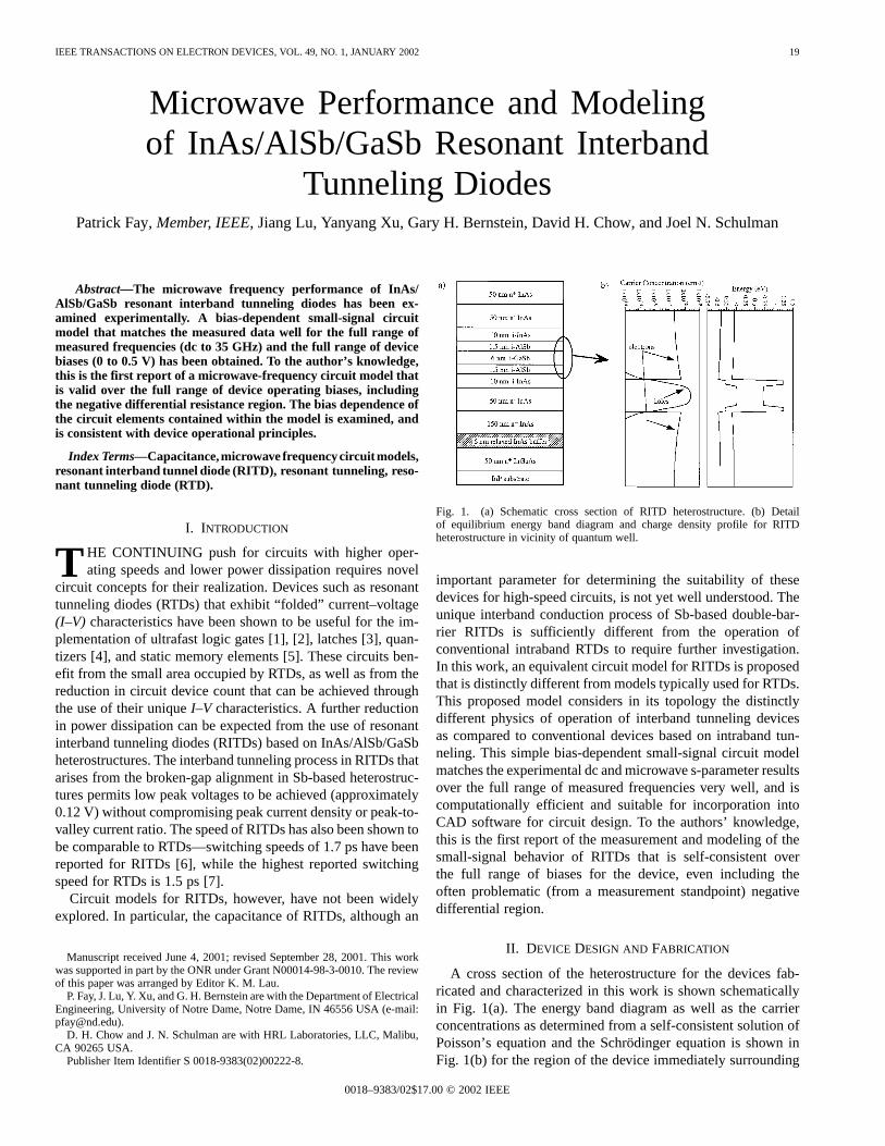
Fig. 6. Comparison of measured and modeled RITD impedance (real andimaginary components) for small-area RITD for three selected biases. Modeledimpedance was determined from small-signal model, measured impedance wascomputed from measured s-parameters. The inset in each figure illustrates thelocation of the bias for the comparison on theI–V characteristic for the RITD.(a) Impedance below current peak, bias voltage= 50 mV. (b) Impedance inNDR region, bias voltage= 0.17 V. (c) Impedance in current valley region,bias voltage= 0.35 V.
curate of a match as obtained with the model shown in Fig. 4. Forexample, employing the models used in [12]–[14] for the RITDunder the bias conditions shown in Fig. 6(b) (biased in the NDRregion with ) resulted in a best-fit root-mean-squareimpedance error of 57.1 from 100 MHz to 35 GHz. Thiscorresponds to an average percent error in impedance magni-
tude of over 8.8% from 100 MHz to 35 GHz. In contrast, useof the model in Fig. 4 for this same bias condition results ina root-mean-square impedance error of 11.1and an averagepercent error in impedance magnitude of 0.95% over the samefrequency range. This suggests that the physics of RITDs, whichare dominated by the interband conduction and the high densityof heavy holes in the quantum well, are sufficiently differentfrom that of intraband devices to require a different approach todevice modeling [15].
To examine the consistency of the s-parameter model andthe dc behavior of the devices, the total dc conductance of themodel,
was compared to the measured dc conductance,
The results of this comparison are shown in Fig. 7 for the small-area device with the parameters shown in Fig. 5. As can be seenin this figure, the dc measured conductance is nearly identical tothat determined from s-parameter measurements. This indicatesthat there are no significant low-frequency effects (e.g., trap orsurface state charging) present—even for very small-area de-vices—since these slow processes would manifest themselvesin dc measurements but not in the s-parameter measurementsfor which the lowest measurement frequency was 100 MHz. Theobserved consistency between dc and microwave circuit modelsalso suggests that the simple equivalent circuit model shown inFig. 4 does not overlook any significant physical processes.
An examination of the qualitative behavior of the small-signalmodel parameters suggests a simple physical interpretation. Asbias is applied to the device, the redistribution of charge inthe quantum well and the band-bending in the InAs spacer andcontact layers are the likely causes for the observed changesin capacitance. For example, changes in quantum well occu-pancy and the formation of an accumulation layer in the topInAs spacer layer/barrier heterointerface are believed to pro-duce the features observed inand . In particular, the peakin does not occur at the same bias voltage as the dc currentpeak, but instead is located approximately at the midpoint ofthe NDR region. This suggests an interpretation forrootedin the separation of holes in the quantum well from electrons inthe InAs spacer and contact layers. Additionally, the relativelyhigh value of at low biases indicates that the InAs contact andspacer layers at equilibrium are not depleted. This is consistentwith the self-consistent Poisson/Schrödinger equilibrium simu-lations shown in Fig. 1(b). The observed decrease inat ele-vated biases is also consistent with the expected onset of spacerlayer depletion. The zero-bias dependence ofon device area,shown in Fig. 8, was found to be well modeled by the expres-sion , where fF/ m fromthe slope of the curve in Fig. 8. The bias dependence of theconductance and capacitance also appear to depend oncharge redistribution; however, as shown in Fig. 8, the zero-biasvalue of is nearly independent of device area (approximately

FAY et al.: MICROWAVE PERFORMANCE AND MODELING OF InAs/AlSb/GaSb 23
Fig. 7. (solid line) Comparison of measured dc conductance and the totallow-frequency ac conductance predicted from the microwave-frequency model(dotted line). The excellent agreement over the full range of biases indicates thatno significant dispersion is present in the devices.
Fig. 8. Dependence of small-signal capacitancec andc as a function ofdevice area. Capacitance c1 is well-modeled byc = c �A+ c withan areal capacitance of 17 fF/�m , while c is nearly independent of devicearea.
100 fF), suggesting that the capacitanceparameterizes a car-rier transit time within the device. This capacitance appears to beloosely analogous to the diffusion capacitance of conventionalpn junction diodes since it originates from charge redistributionwithin the device, and like conventional diffusion capacitancecan be considerably larger than the corresponding electrostaticgeometric capacitances. On the other hand, the conductanceis dominated by the fundamental density-of-states and conser-vation of momentum effects that lead to negative differential re-sistance in RITDs.
Within this simple interpretation, the dramatic differences inbias dependence betweenand , and and are not un-expected; however, the asymmetry at zero bias may initially besurprising since the heterostructure and dcI–V characteristic isnearly symmetric. As can be seen in Fig. 5, at zero biasismuch lower than , and is also much lower than . Attempts
to enforce zero-bias symmetry in the model resulted in poor fitsto the measured s-parameters. The asymmetry may be justified,however, despite the apparent symmetry in the heterostructureas depicted in Fig. 1(a), since the parameters, , and ,do not simply represent the conductance and capacitance asso-ciated with tunneling through two isolated, identical barriers inthe device. Instead, they represent the unique physical processesinherent to the RITD structure that give rise to transport into andout of the quantum well, respectively. Thus, although continuityrequires the dc current through both transport processes to be thesame, the small-signal conductances and capacitances need notbe identical.
The bias dependence of these parameters is somewhatdifferent from that previously reported [10]. In this previouswork, a clear increase in capacitance was observed as the biasapproached the NDR region, and some deviation betweenthe small-signal resistance and the measured dc differentialresistance was also apparent. In this work, neither of thesephenomena were observed. We did, however, observe be-havior similar to that in [10] if network analyzer port powersgreater than 38 dBm were used in the measurements. Theselarger port powers produce a broadening of the microwavesmall-signal capacitance and conductance peaks due to over-driving of the strong RITD nonlinearities. The power level usedin [10] was not reported.
IV. CONCLUSION
The bias dependence of the microwave frequency per-formance of InAs/AlSb/GaSb RITDs has been determinedexperimentally. The model developed matches the measureds-parameters of fabricated devices well over the full range offrequencies and bias conditions. To the author’s knowledge,this is the first report of a microwave-frequency circuit modelthat is valid over the full range of device operating biases,including the negative differential resistance region. By in-vestigating the microwave performance of small-area RITDs,devices with sufficiently small conductances to be stable fors-parameter measurement have been measured and a modelthat describes the observed behavior well has been obtained.The circuit elements contained within the model vary smoothlywith bias, and the small-signal microwave conductances areconsistent with dcI–V measurements.
ACKNOWLEDGMENT
The authors would like to thank L. Warren, C. Haeussler, andK. Holabird for their technical assistance, and T. P. E. Broekaertfor useful discussions. P. Fay is grateful for the support and en-couragement of G. Wiskirchen.
REFERENCES
[1] K. Maezawa, H. Matsuzaki, M. Yamamoto, and T. Otsuji, “High-speedand low-power operation of a resonant tunneling logic gate MOBILE,”IEEE Electron Device Lett., vol. 19, pp. 80–82, Mar. 1998.
[2] W. Williamson, III, S. B. Enquist, D. H. Chow, H. L. Dunlap, S. Subra-maniam, P. Lei, G. H. Bernstein, and B. K. Gilbert, “12 GHz clocked op-eration of ultralow power interband resonant tunneling diode pipelinedlogic gates,”IEEE J. Solid-State Circuits, vol. 32, pp. 222–231, Feb.1997.
24 IEEE TRANSACTIONS ON ELECTRON DEVICES, VOL. 49, NO. 1, JANUARY 2002
[3] K. Sano, K. Murata, T. Otsuji, T. Akeyoshi, N. Shimizu, and E. Sano,“An 80-Gb/s optoelectronic delayed flip-flop IC using resonant tun-neling diodes and uni-traveling-carrier photodiode,”IEEE J. Solid StateCircuits, vol. 36, pp. 281–289, Feb. 2001.
[4] T. P. E. Broekaert, B. Brar, J. P. A. van der Wagt, A. C. Seabaugh, F.J. Morris, T. S. Moise, E. A. Beam, and G. A. Frazier, “A monolithic4-Bit 2-Gsps resonant tunneling analog-to-digital converter,”IEEE J.Solid-State Circuits, vol. 33, pp. 1342–1349, Sept. 1998.
[5] J. P. A. van der Wagt, A. C. Seabaugh, and E. A. Beam, III, “RTD/HFETlow standby power SRAM gain cell,”IEEE Electron Device Lett., vol.19, pp. 7–9, Jan. 1998.
[6] E. Ozbay, D. M. Bloom, D. H. Chow, and J. N. Schulman, “1.7-ps,microwave, integrated-circuit-compatible InAs/AlSb resonant tunnelingdiodes,”IEEE Electron Device Lett., vol. 14, pp. 400–402, Aug. 1993.
[7] N. Shimizu, T. Nagatsuma, T. Waho, M. Shinagawa, M. Yaita, andM. Yamamoto, “In Ga As/AlAs resonant tunnelling diodeswith switching time of 1.5 ps,”Electron. Lett., vol. 31, no. 19, pp.1695–1697, 1995.
[8] I. H. Tan, G. L. Snider, and E. L. Hu, “A self-consistent solution ofSchrodinger–Poisson equations using a nonuniform mesh,”J. Appl.Phys., vol. 68, pp. 4071–4076, 1990.
[9] P. Fay, J. Lu, Y. Xu, G. H. Bernstein, D. H. Chow, J. N. Schulman, H.L. Dunlap, and H. J. De Los Santos, “Fabrication of monolithically-integrated InAlAs/InGaAs/InP HEMT’s and InAs/AlSb/GaSb resonantinterband tunneling diodes,”IEEE Trans. Electron Devices, vol. 48, pp.1282–1284, June 2001.
[10] K. Fobelets, R. Vounckx, J. Genoe, G. Borghs, H. Gronqvist, andL. Lundgren, “High-frequency capacitances in resonant interbandtunneling diodes,”Appl. Phys. Lett., vol. 64, no. 19, pp. 2523–2525,1994.
[11] J. Genoe, C. Van Hoof, W. Van Roy, J. H. Smet, K. Fobelets, R. P.Mertens, and G. Borghs, “Capacitances in double-barrier tunnelingstructures,”IEEE Trans. Electron Devices, vol. 38, pp. 2006–2012,Sept. 1991.
[12] J. Jo, K. Alt, and K. L. Wang, “Effect of doping density on capaci-tance of resonant tunneling diodes,”J. Appl. Phys., vol. 82, no. 10, pp.5206–5209, 1997.
[13] T. Wei, S. Stapleton, and E. Berolo, “Equivalent circuit and capacitanceof double barrier resonant tunneling diode,”J. Appl. Phys., vol. 73, no.2, pp. 829–834, 1993.
[14] J. J. M. Kwaspen, M. I. Lepsa, Th. G. van de Roer, and W. van derVleuten, “Accurate equivalent-network modeling of GaAs/AlAs basedresonant tunneling diodes with thin barrier layers,”Electron. Lett., vol.33, no. 19, pp. 1657–1658, 1997.
[15] V. Duez, M. Chaubet, O. Vanbesien, and D. Lippens, “Optical switchingof resonant interband tunnelling diodes induced by heavy hole spacecharge effects,”Electron. Lett., vol. 36, no. 11, pp. 974–975, 2000.
Patrick Fay (S’89–M’97) received the B.S. degree in electrical engineeringfrom the University of Notre Dame, Notre Dame, IN, in 1991 and the M.S. andPh.D. degrees in electrical engineering from the University of Illinois at Urbana-Champaign (UIUC) in 1993 and 1996, respectively.
From 1992 to 1994, he was a National Science Foundation Graduate ResearchFellow, and he served as a Visiting Assistant Professor in the Department ofElectrical and Computer Engineering at UIUC in 1996 and 1997. He is cur-rently an Assistant Professor in the Department of Electrical Engineering at theUniversity of Notre Dame. His research interests include the design, fabrication,and characterization of high-speed optoelectronic and microwave electronic de-vices and circuits.
Dr. Fay is a member of the IEEE Electron Devices Society and the IEEEMicrowave Theory and Techniques Society.
Jiang Lu received the B.S. degree in physics from Peking University, China, andthe M.S. in physics from the University of Science and Technology of China. Hereceived the M.S. in electrical engineering from the University of Notre Dame,South Bend, IN.
He is currently a Senior Engineer at Atmel Corporation, Colorado Springs,CO.
Yanyang Xu received the B.S. and M.S. degrees from Xidian University, Chinaand the Hebei Semiconductor Research Institute (HSRI), China, respectively.While at HSRI, she worked as a Circuit Design and Test Engineer. She ispresently pursuing the Ph.D. in electrical engineering at the University of NotreDame, Notre Dame, IN. Her research activities focus on the design, fabrication,and test of high-speed electronic circuits and devices.
Gary H. Bernstein received the B.S.E.E. from the University of Connecticut,Storrs, in 1979 and the M.S.E.E. from Purdue University, West Lafayette, IN,in 1981. He received the Ph.D. from Arizona State University, Tempe, in 1987,where he spent a year as a postdoctoral fellow.
During the summers of 1979 and 1980, he was a Graduate Assistant at LosAlamos National Laboratory and in the summer of 1983, he interned at theMotorola Semiconductor Research and Development Laboratory, Phoenix, AZ.He joined the Department of Electrical Engineering at the University of NotreDame, Notre Dame, IN, in 1988 as an Assistant Professor, and became Directorof the Microelectronics Laboratory in 1989.
Dr. Bernstein received an NSF White House Presidential Faculty FellowAward in 1992, was promoted to rank of Professor in 1998, and is currentlythe Associate Chair of the Department of Electrical Engineering. He hasauthored or coauthored more than 80 publications in the areas of electron beamlithography, quantum electronics, ultrahigh speed integrated circuits, reliabilityof ULSI components, and ULSI processing.
David H. Chow received the B.S. degree in applied physics from Case WesternReserve University, Cleveland, OH, in 1984, and the M.S. and Ph.D. degrees inapplied physics from the California Institute of Technology, Pasadena, in 1986and 1989, respectively.
In 1990, he joined HRL Laboratories, Malibu, CA, where he is currentlya Department Manager and Senior Research Scientist in the MicroelectronicsLaboratory. His research interests focus on semiconductor heterostructures foradvanced electronic and optoelectronic devices. He has performed extensive re-search in molecular beam epitaxy of arsenide/antimonide device structures. Hehas authored or coauthored more than 100 articles in refereed scientific journals.
Joel N. Schulmanjoined HRL Laboratories, Malibu, CA, in 1984. His researchinterests include superlattices for infrared detector materials, the band structureand optical properties of III–V semiconductor superlattices, and novel tunnelstructures for device application. He is also an Adjunct Professor in the Elec-trical Engineering Department at the University of California, Los Angeles.