Embed Size (px)
Citation preview

Molecular Electronics
Amy Szuchmacher BlumMcGill University
Department of Chemistry

Outline
• Why use molecules?
• Making molecular measurements
• Conduction in molecules
• Molecular switches

Moore’s Law
www.intel.com
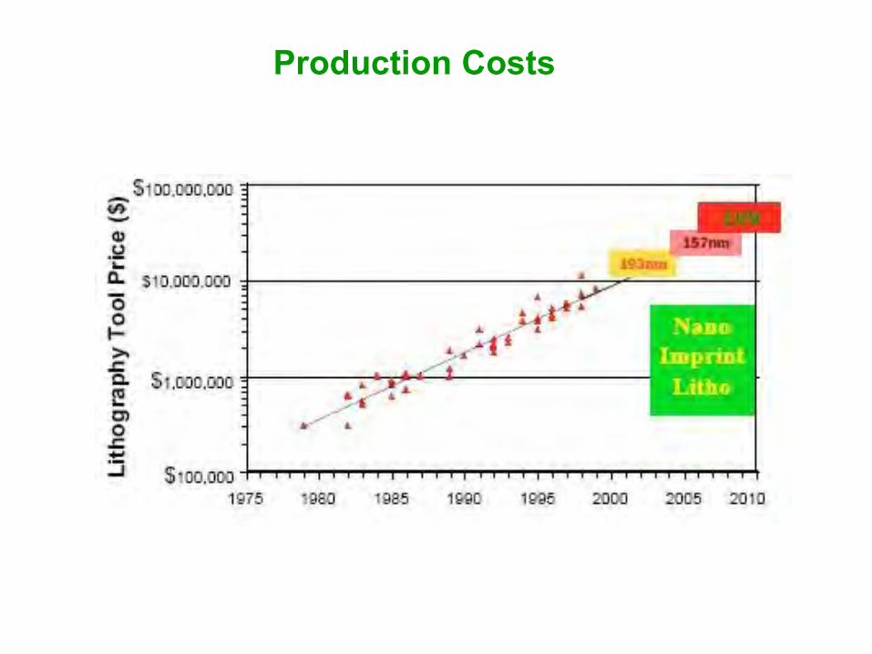
Production Costs

Technical Challenges
target

Molecular Measurements

Basic 2 Terminal Device
Elucidate the roles that “alligator clips”, metals and the molecular core play in defining I-V
characteristics
molecular core
“alligator clips”
metals

“Alligator Clips”
Attach molecules to surface and drive the self-assembly process
“Connect” molecular electronic structure to the metallic band structure
Reed and Tour Scientific American June 2000

Electronic Characterization Methods
Scanning Probes
Nanopore Hg Drop
S S
Au{111}
S
STM Tip trajectory
STM Tip
S SS SSS S S S S
Break Junction Crosswire Junction

Break Junction
QuickTime™ and a decompressor
are needed to see this picture.
Advantages: Can measure single molecules
Electrical contact to device easy
Stable to T change (low T)
Y. Selzer et al. Nano Lett 5, 61 (2005).

Break Junction Measurements
QuickTime™ and a decompressor
are needed to see this picture.QuickTime™ and a
decompressorare needed to see this picture.
H.B. Weber et al. Physica E, 18, 231 (2003).

SAM in Nanopore
QuickTime™ and a decompressor
are needed to see this picture.
QuickTime™ and a decompressor
are needed to see this picture.
M.A. Reed Proc IEEE, 87, 652 (1999).
Advantages: SAM formation well understood
Stable once formed (T, V, molecular decompostion)
High yield of functional devices

Problems With the Top Electrode
QuickTime™ and a decompressor
are needed to see this picture.
A. V. Walker et al. Appl. Phys. Lett., 84, 4008 (2005).
Hot metal reacts with SAM (ex: Ti)
Hot metal doesn’t stick to SAM (ex: Au)

Crossed Wire Tunnel Junction
S SAu
Au
• Simple experimental apparatus • Wide variety of wires available (Au, Pd, Pt, …)• Junction contains ~103 molecules• No metallization after SAM deposition

Thiolate-Metal Interaction
Higher conductivity corresponds to hole injection at the Pd-S interface.
Lower barrier for Pd-S compared to Au-S contact consistent with theoretical predictions.
SSAu Pd

SPM techniques

• Molecular junctions made using metal coated AFM tips to contact self-assembled monolayers
• Junction resistance measured as a function of molecular length and contact type
C. Daniel Frisbie University of Minnesota
Conducting Probe AFM

Current vs. Voltage Measurements on Single Molecules
crystalline undecanethiol
(C11) SAM
insert dithiol molecule at defect
sites
bind 2 nm gold nanoparticles to inserted dithiols
25 nm x 25 nm 75 nm x 75 nm 75 nm x 75 nm
A. S. Blum et al. Appl. Phys. Lett., 82, 3322 (2003).

Molecular Film vs. Isolated Molecule
•Intermolecular hopping does not contribute to conductance
-0.08
-0.06
-0.04
-0.02
0
0.02
0.04
0.06
-0.1 -0.06 -0.02 0.02 0.06 0.1
bias (V)
curr
ent (
nA)
monocomponent OPE SAM OPE inserted in C11 SAM
monocomponent OPE SAM
OPE inserted into C11 SAM
A. S. Blum et al. Appl. Phys. Lett., 82, 3322 (2003).

Two Layer Tunnel Junction Model
L. A. Bumm et al. J. Phys. Chem. B., 103, 8122 (1999).
Layer Transconductance:
G = G0 exp(-bihi)
Constant Current Imaging:
GC11 Ggap = GOPV Ggap
b2 = [bC11hc11-a(DSTM-Dh)]/h2

Determining b via STM Imaging
A. S. Blum et al. J. Am. Chem. Soc., 127, 10010 (2005).
Apparent height represents convolution of topography and electronic information.

Molecular Decay Constants
molecule length(Å)
STM apparent height
(Å)
b(Å-1)
C11 12.5 0 1.2
OPE 20.2 4.3 1.03±0.13
OPV 19.3 10.0 0.40±0.12
Ru-OPE (S to final C) 22.4 7.8 0.88±0.12
Ru-OPE(S to final Ru) 18.6 7.8 0.59±0.08
D. S. Seferos et al. J. Am. Chem. Soc., ASAP (2006).
A. S. Blum et al. J. Am. Chem. Soc., 127, 10010 (2005).

Multiple Break Junction Formation
QuickTime™ and a decompressor
are needed to see this picture.
QuickTime™ and a decompressor
are needed to see this picture.
Z. Huang et al. J. Am. Chem. Soc., 129, 13225 (2007).
Advantages: Good statistics
Probes local environment
Don’t need monolayer
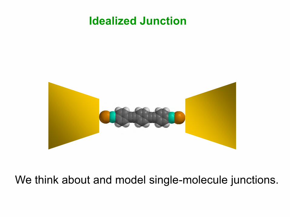
Idealized Junction
We think about and model single-molecule junctions.

Measuring an Ensemble of Molecules
Are the properties of molecular wires in a metal-molecule-metal
junction additive? Does G = nG0

Theoretical Predictions
M. Magoga and C. Joachim, Phys. Rev. B 59, 16011 (1999).
S. N. Yaliraki and M. A. Ratner, J. Chem. Phys. 109, 5036
(1998).
N. D. Lang and P. Avouris, Phys. Rev. B 62, 73257329 (2000).

Measurements on Alkanes
Cui, X. D.; Primak, A.; Zarate, X.; Tomfohr, J.; Sankey, O. F.; Moore, A. L.; Moore, T. A.; Gust, D.; Harris, G.; Lindsay, S. M. Science 2001, 294, 571-574.

Scaling of Parallel Molecular Wires
sample molecular structure length(nm)
crossed wire
resistance
STM resistance
OPE 2.02 1.7 ± 0.6 MW 1.7 ± 0.4 GW
OPV 2.07 0.5 ± 0.2 MW 0.6 ± 0.1 GW
A.S. Blum et al., J. Phys. Chem. B, 108, 18124 (2004).

Scaling of Molecular Wires in Parallel
Molecular wires act as discrete non-interacting conductance channels (i.e. G = nG0)

Possible Conduction Mechanisms
resonanttunneling
non-coherent charge carrier hopping
non-resonanttunneling
Dominant Mechanisms for Short Molecules

Conduction via Tunneling
QuickTime™ and a decompressor
are needed to see this picture.
Y. Selzer et al. Nano Lett 5, 61 (2005).
Arrhenius plot of current vs. 1/T at bias voltage 0.1 V to 1 V

Basic 2 Terminal Device
molecular coreOBu
BuO

Structure Dependence of Charge Transport
S SAu Au
SSAu
Au
S
SAu
Au
OBu
BuO
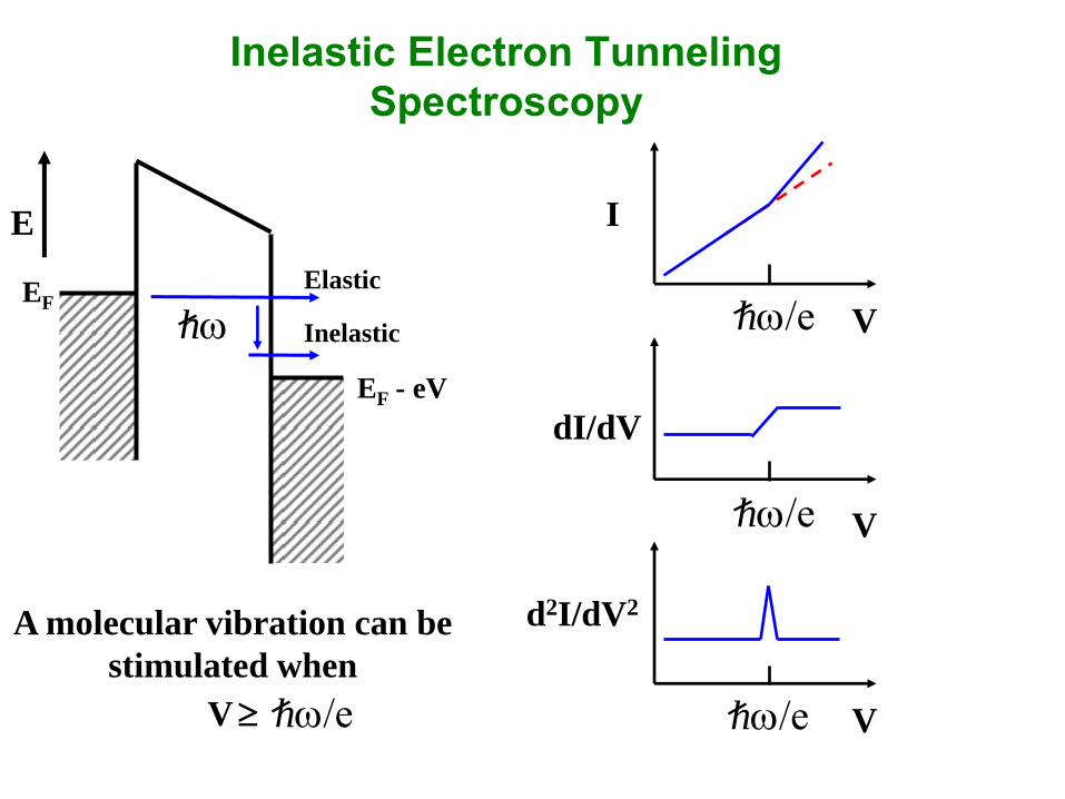
Inelastic Electron Tunneling Spectroscopy
Elastic
Inelastic
E
EF
h
EF - eV
A molecular vibration can be
stimulated when
V h/e
I
dI/dV
d2I/dV2
V
V
Vh/e
h/e
h/e

IETS of Alkane Thiol
Observation of both IR and Raman vibrational modes
C-H str.
CH2 rock
v(C-C)T
CH2 wag
Jason Lazorcik, James G. Kushmerick

IETS of Molecular Junctions
HS
AcS SAc
AcSSAc
C11
OPV
OPE
C11
OPE OPV
Nano Letters 4 (2004) 639-642.

In Junction Optical Spectroscopy
QuickTime™ and a decompressor
are needed to see this picture.
D.R. Ward et al. Nano Lett 8, 918 (2008).

Correlated Optical and Conduction Measurements
QuickTime™ and a decompressor
are needed to see this picture.
D.R. Ward et al. Nano Lett 8, 918 (2008).
Outline
• Motivation
• Switching in Molecules
• Virus as a scaffold
• Making molecular circuits
• Molecular memory devices

Molecular Electronics
• How can we make molecular switches?
• Once we have switches, how can we make electrical contact?

Switching in Molecules

Previous Examples of Molecular Switching
Reed/Tour switch in nanopore
voltage based switching
Weiss group (2001), Lindsay group (2003), others switch in STM
stochastic switching
Z. J. Donhauser, et. al, Science 292, 2303-2307 (2001).
Reed et al. Applied Physics Letters
78 (2001) 3735-3737.

Current vs. Voltage Measurements on Single Molecules
crystalline undecanethiol
(C11) SAM
insert dithiol molecule at defect
sites
bind 2 nm gold nanoparticles to inserted dithiols
25 nm x 25 nm 75 nm x 75 nm 75 nm x 75 nm
A. S. Blum et al. Appl. Phys. Lett., 82, 3322 (2003).

Stochastic Switching
molecule matrix reference
dodecanethiol(C12)
Z.J. Donhauser et al. Science, 292, 2303 (2001).
decanethiol(C10)
G. K. Ramachandran et al. Science, 300, 1413 (2003).
dodecanethiol(C12)
decanethiol(C10)
R. A. Wassel et al. Nano Lett., 3, 1617 (2003).
undecanethiol(C11)
A. S. Blum et al. Nat. Mater.,
5,167 (2005).

Stochastic Switching
Measurements made at constant bias voltage (1V)
Stochastic switching is dynamic—molecules switch on and off

Molecular Film vs. Isolated Molecule
•Intermolecular hopping does not contribute to conductance
-0.08
-0.06
-0.04
-0.02
0
0.02
0.04
0.06
-0.1 -0.06 -0.02 0.02 0.06 0.1
bias (V)
curr
ent (
nA)
monocomponent OPE SAM OPE inserted in C11 SAM
monocomponent OPE SAM
OPE inserted into C11 SAM
A. S. Blum et al. Appl. Phys. Lett., 82, 3322 (2003).

I/V Measurements on BPDN SAMs
A. S. Blum et al. Nat. Mater., 5, 167 (2005)

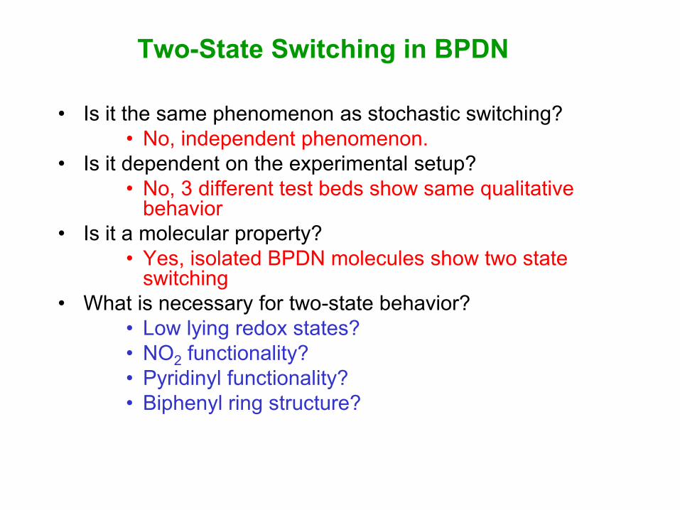
Two-State Switching in BPDN
• Is it the same phenomenon as stochastic switching?
• Is it dependent on the experimental setup?
• Is it a molecular property?

Two-State Switching in BPDN
• Is it the same phenomenon as stochastic switching?
• Is it dependent on the experimental setup?
• Is it a molecular property?

0
0.2
0.4
0.6
0.8
1
1.2
0 0.5 1 1.5 2
bias (V)
curr
ent (
nA)
Voltage Controlled Switching in STM
500 mV21 500 mV
500 mV (molecules off)
2
1
500 mV (molecules on)
Bias history changes imaging properties of inserted molecules.
Change in molecule appearance is due to
state change, NOT bias dependent imaging
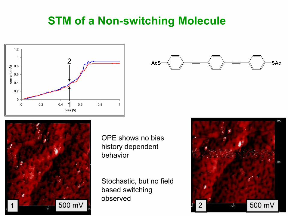
STM of a Non-switching Molecule
0
0.2
0.4
0.6
0.8
1
1.2
0 0.2 0.4 0.6 0.8 1
bias (V)
curr
ent (
nA)
2
1
OPE shows no bias history dependent behavior
Stochastic, but no field based switching observed
1 500 mV 500 mV2

Two-State Switching in BPDN
• Is it the same phenomenon as stochastic switching?
• Is it dependent on the experimental setup?
• Is it a molecular property?

SEM images of micromagnetic trap (MMT)(a) Central region of MMT device.(b) Image of magnetic proximal probe tips.
D. Long et al., Adv. Mater., 16, 814 (2004).
I
V
SEM image of microsphere junction
N S
Magnetic Entrapment of Metallized Silica Microspheres

Crossed-Wire Test Bed
PRL 89, 086802 (2002)JACS 124, 10654-10655 (2002)
JACS 125, 3202-3203 (2003)Nano Letters 3, 897-900 (2003)

Conductance Scaling
1
1000
100-300
D. Long et al., Adv. Mater., 16, 814 (2004).A.S. Blum et al., J. Phys. Chem. B, 108, 18124 (2004).

Molecular Memory Studied by Three Techniques
Consistent switch signature
observed for same molecule in three independent test-
beds.
BPDN
A. S. Blum et al. Nat. Mater., 5, 167 (2005)

Two-State Switching in BPDN
• Is it the same phenomenon as stochastic switching?
• Is it dependent on the experimental setup?
• Is it a molecular property?

Single Molecule Measurements
I
Over 2nm particle
-1.5
-1.0
-0.5
0.0
0.5
1.0
1.5
-2 -1.5 -1 -0.5 0
bias (V)
curr
ent (
nA)
Over C11 film
-1.5
-1.0
-0.5
0.0
0.5
1.0
1.5
-2 -1.5 -1 -0.5 0
bias (V)
curr
ent (
nA)
In I/V curves, 2 states observed for BPDN molecule, but not for C11 alkane

Controllable Switching
0.0
2.0
4.0
6.0
8.0
10.0
12.0
-0.5 -0.4 -0.3 -0.2 -0.1 0 0.1
Bias (V)
Cur
rent
(Offs
et) n
A
h
Controlled switching between states induced by running bias through 0 V
Conductance state can be controlled by the applied voltage
Bias offset demonstrates charging in molecule or film

Reproducibility
-2.0
-1.0
0.0
1.0
2.0
3.0
4.0
5.0
6.0
-3 -2.5 -2 -1.5 -1 -0.5 0
bias (V)
curr
ent (
nA) [
offs
et fo
r cla
rity]
1
10
20
45
Switching between high conductivity state and low conductivity state is reproducible as long as tip stays over moleculeSwitching between high conductivity state and low conductivity state is
reproducible as long as tip stays over molecule

ReproducibilityE. Lörtscher et al. Small 2, 973 (2006).
J. He et al. JACS 128, 14828 (2006).
Z.K. Keane et al., Nano Lett. 6, 1518 (2006).

Two-State Switching in BPDN
• Is it the same phenomenon as stochastic switching?
• Is it dependent on the experimental setup?
• Is it a molecular property?
• What is necessary for two-state behavior?

Switching Mechanisms
Bias offset demonstrates charging in molecule or film
Au
SH
SH
SH
SH
SH
SHSH SH SHSH SH SH SH SH SHSH SH SHSH SH SH SH SHSHSHSH
Au
2 nm Au
Au
SH
SH
SH
SH
SH
SHSH SH SHSH SH SH SH SH SHSH SH SHSH SH SH SH SHSHSHSH
Au
SH
SH
SH
SH
SH
SHSH SH SHSH SH SH SH SH SHSH SH SHSH SH SH SH SHSHSHSH
Au
2 nm Au
Two-State Switching in BPDN
• Is it the same phenomenon as stochastic switching?• No, independent phenomenon.
• Is it dependent on the experimental setup?• No, 3 different test beds show same qualitative
behavior• Is it a molecular property?
• Yes, isolated BPDN molecules show two state switching
• What is necessary for two-state behavior?• Low lying redox states?• NO2 functionality?• Pyridinyl functionality?• Biphenyl ring structure?

Redox Active Molecules as Switches
Ru1Ru2
NN
SSiMe3
4
11.62
15.4
Ru1Ru2
NN 4
SSiMe3
18.62
22.4
Compund 1, distances are crystallographically determined
Compund 2, distances are estimated based on that of 1
Designing a molecular switch:
Low-lying redox states
Conjugated system for conductance
Tong Ren, Purdue A. S. Blum et al. J. Am. Chem. Soc., 127, 10010 (2005).

Redox Active, No Switching!
-1.50
-1.00
-0.50
0.00
0.50
1.00
1.50
-1 -0.75 -0.5 -0.25 0 0.25 0.5 0.75 1
bias (V)
curr
ent (
nA)
Single redox wave with a formal potential (vs. Ag/AgCl/KCl) of E = 0.40 V
Stochastic switching, but no two state behavior in I/V.
Scott Trammel, NRL

Two-State Switching in BPDN
• Is it the same phenomenon as stochastic switching?• No, independent phenomenon.
• Is it dependent on the experimental setup?• No, 3 different test beds show same qualitative behavior
• Is it a molecular property?• Yes, isolated BPDN molecules show two state switching
• What is necessary for two-state behavior?• Low lying redox states? NO!• NO2 functionality?• Pyridinyl functionality?• Biphenyl ring structure?

What is needed for switching?
Molecules courtesy Jim Tour
N
SAc
N
SAc
O2N
NO2
N
SAc
N
SAc
SAc
SAc
SAc
SAc
NO2
NO2
SAc
SAc
O2N
NO2
SAc
SAc
BPDN trans-DN cis-DN BP Biphen OPE

Biphenyl-Dinitro
N
AcS
N
SAc
NO2
O2N95% of all molecules probed show 2-state behavior
For any given molecule, 90% of the I/V traces show 2-state behavior
Large change in conductance: high to low ratio is 30 ± 10

Biphenyl
AcS SAc
No two-state behavior observed

Cis-Dinitro
AcS SAc
O2NO2N 85% of all molecules probed show 2-state behavior
For any given molecule, 80% of the I/V traces show 2-state behavior
Large change in conductance: high to low ratio is 15 ± 8
Bias offset seen for high conductive state, as in BPDN

Bipyridyl
N
AcS
N
SAc 83% of all molecules probed show 2-state behavior
For any given molecule, 20% of the I/V traces show 2-state behavior
Small change in conductance: high to low ratio is 3.5 ± 2
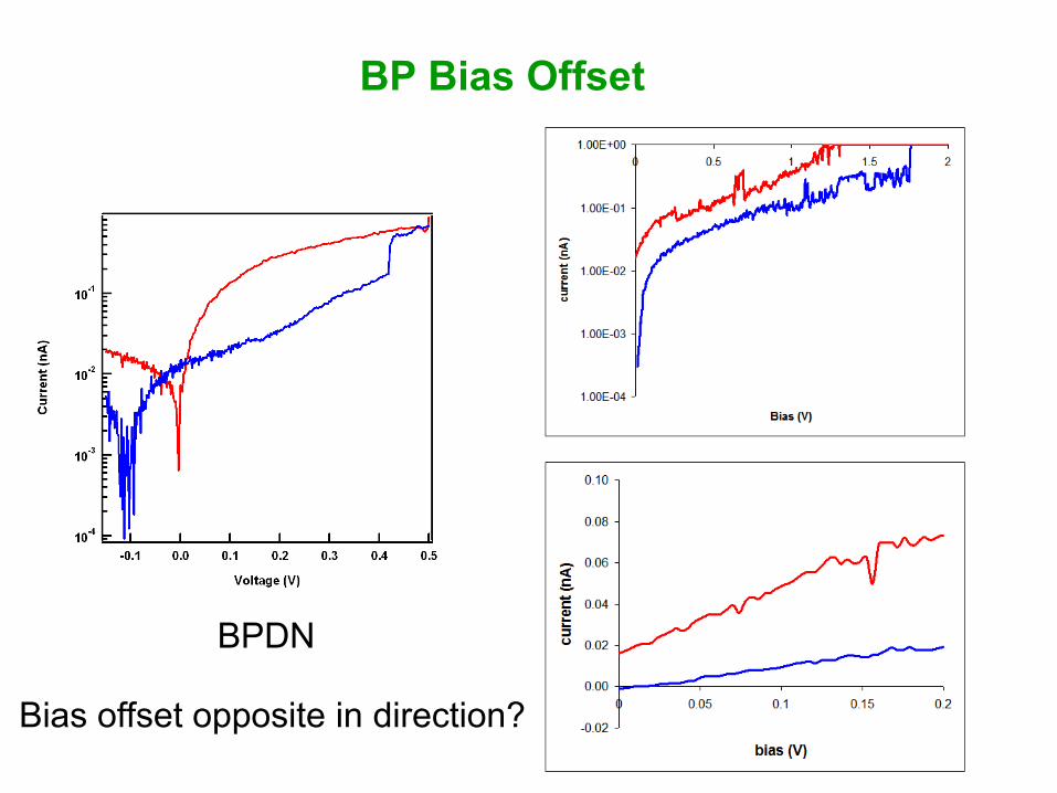
BP Bias Offset
BPDN BP
Bias offset opposite in direction?

Polaron Model
-1.50
-1.00
-0.50
0.00
0.50
1.00
1.50
-2.5 -1.5 -0.5 0.5 1.5 2.5
bias (V)cu
rren
t (nA
)
M. Galperin, M. A. Ratner, and A. Nitzan Nano Lett. 5, 125 (2005).

Conductance and Switching
molecule length(Å)
STM apparent height (Å)
b(Å-1)
C11 12.5 0 1.2
OPE 20.2 4.3 1.03±0.13
Biphenyl 24.1 5.1 1.16±0.31
Bipyridyl 24.1 5.3 1.14±0.25
Bipyridyl-Dinitro 24.1 9.3 0.73±0.18
Biphenyl and substituted biphenyls in the low state show the same measured current at 1 V.

What is needed for switching?
N
AcS
N
SAc
NO2
O2N
AcS SAc
O2NO2N
N
AcS
N
SAc
• Molecules with NO2groups have “strong” switching signatures.
• Smaller switching signature still present for pyridyl molecule without NO2 groups!
• No switching for molecule lacking both NO2 and pyridyl groups.
AcS SAc

What is Needed for Switching?
N
AcS
N
SAc
NO2
O2N
AcS SAc
NO2
O2N
AcS SAc
O2NO2N
N
AcS
N
SAc
AcS SAc
AcS SAc
Molecular Structure Switching
Yes
Yes
Yes
Yes (Minimal)
No
No
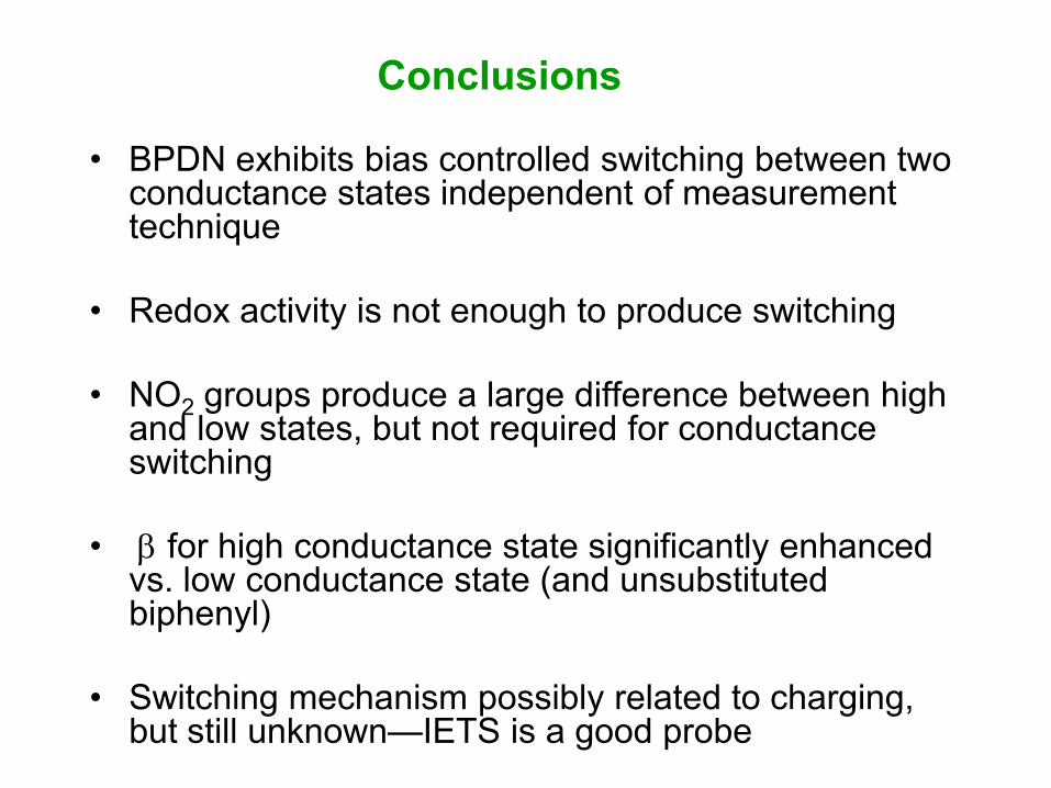
Conclusions
• BPDN exhibits bias controlled switching between two conductance states independent of measurement technique
• Redox activity is not enough to produce switching
• NO2 groups produce a large difference between high and low states, but not required for conductance switching
• b for high conductance state significantly enhanced vs. low conductance state (and unsubstituted biphenyl)
• Switching mechanism possibly related to charging, but still unknown—IETS is a good probe

Acknowledgements
NRL Rice UniversityJohn C. Yang James M. TourCharles M. Patterson Yuxing Yao Banahalli R. Ratna Jay C. HendersonMartin H. MooreScott Trammell
SAIC Purdue UniversityRanganathan Shashidhar Tong RenDavid P. Long
NIST FundingJames G. Kushmerick DARPA, ONR