Embed Size (px)
Citation preview
Freescale SemiconductorProduct Brief
Document Number: MPC560xSPBRev. 4, 04/2011
Contents
MPC5606S Microcontroller Product Brief32-bit MCU for cluster applications with stepper motor, TFT graphic controller and LCD driver
Introduction . . . . . . . . . . . . . . . . . . . . . . . . . . . . . . . . . . . . 2Block diagram . . . . . . . . . . . . . . . . . . . . . . . . . . . . . . . . . . 2Overview of the MPC5606S microcontroller . . . . . . . . . . . 33.1 Device comparison . . . . . . . . . . . . . . . . . . . . . . . . . 43.2 Feature list. . . . . . . . . . . . . . . . . . . . . . . . . . . . . . . . 53.3 Feature details. . . . . . . . . . . . . . . . . . . . . . . . . . . . . 8Application examples . . . . . . . . . . . . . . . . . . . . . . . . . . . 274.1 Instrument cluster with TFT display. . . . . . . . . . . . 274.2 Instrument cluster with LCD segment display . . . . 28Developer support . . . . . . . . . . . . . . . . . . . . . . . . . . . . . . 29Orderable parts . . . . . . . . . . . . . . . . . . . . . . . . . . . . . . . . 30Revision history. . . . . . . . . . . . . . . . . . . . . . . . . . . . . . . . 31
The MPC5606S family represents a new generation of 32-bit microcontrollers based on the Power Architecture®. These devices are targeted to address the next wave of automotive instrument cluster applications driven by significant growth in demand for color Thin Film Transistor (TFT) displays within the vehicle. The advanced and cost-efficient processor core of the family complies with the Power Architecture embedded category, which is 100% user-mode compatible with the original PowerPC user instruction set architecture (UISA). It offers high performance processing optimized for low power consumption, operating at speeds up to 64 MHz. The family itself is fully scalable from 256 KB up to 1 MB internal flash memory. The memory capacity can be further expanded via the on-chip QuadSPI serial flash controller module. Larger memory versions with greater graphics functionality are planned for the future.
The MPC5606S family benefits from the extensive development infrastructure for Power Architecture devices which is already well established. This includes
123
4
567
© Freescale Semiconductor, Inc., 2008–2011. All rights reserved.
Introduction
full support from available software drivers, operating systems and configuration code to assist with users' implementations. See Section 5, “Developer support,” for more information.
The MPC5606S family platform has a single level of memory hierarchy supporting on-chip SRAM and flash memories. The 1 MB flash version (MPC5606S) features 160 KB of on-chip graphics SRAM to buffer cost effective color TFT displays driven via the on-chip Display Control Unit (DCU). See Table 1 for specific memory and feature sets of the product family members.
1 IntroductionThe MPC5606S family of microcontrollers are designed to reduce development and production costs of TFT-based instrument cluster displays by providing a single-chip solution with the processing and storage capacity to host and execute real-time application software and drive the TFT display directly. Operating at speeds of up to 64 MHz, these devices offer high performance processing with low power consumption. Memory and storage capacity can be further expanded via the on-chip Serial Peripheral Interface (SPI) and QuadSPI peripheral modules.
The MPC5606S platform features up to 1 MB of on-chip flash memory, up to 160 KB of on-chip graphics SRAM and an on-chip Display Control Unit (DCU) designed to drive color TFT displays.
MPC5606S devices are compatible with the existing development infrastructure of current Power Architecture devices and are supported with software drivers, operating systems and configuration code to assist with application development. See Section 5, “Developer support,” for more information.
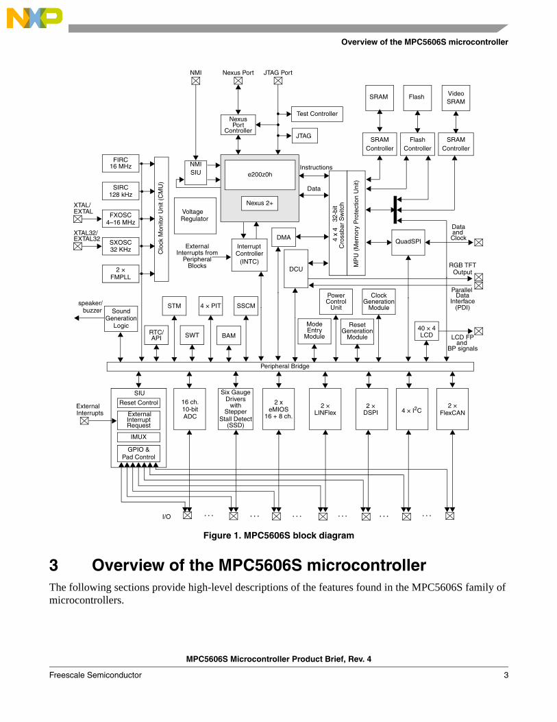
2 Block diagramFigure 1 shows a top-level block diagram of the MPC5606S microcontroller.
MPC5606S Microcontroller Product Brief, Rev. 4
Freescale Semiconductor2
Overview of the MPC5606S microcontroller
Figure 1. MPC5606S block diagram
3 Overview of the MPC5606S microcontrollerThe following sections provide high-level descriptions of the features found in the MPC5606S family of microcontrollers.
Six GaugeDrivers
withStepper
Stall Detect(SSD)
16 + 8 ch.
2 ×DSPI
Test Controller
Nexus 2+
Nexus
SIU
Reset Control
Interrupt
External
IMUX
GPIO &
JTAG
Cro
ssba
r S
witc
h
Pad Control
JTAG PortNexus Port
e200z0h
External
Blocks
32-b
it
Controller
2 ×FlexCAN
4 x
4
Peripheral Bridge
PeripheralInterrupts from
InterruptRequest
ExternalInterrupts
I/O
Instructions
Data
VoltageRegulator
NMI
SWT
STM
NMISIU
. . . . . . . . .. . .
(INTC)
4 × I2C
. . .
2 ×LINFlex
2 xeMIOS
16 ch.
ADC
MP
U (
Mem
ory
Pro
tect
ion
Uni
t)
Clo
ck M
onito
r U
nit (
CM
U)
ControllerFlash
Flash
PowerControl
ModeEntry
ClockGeneration
Module
ResetGeneration
Module
Unit
ModuleBAMRTC/
SSCM
API
10-bit
. . .
DMA
DCURGB TFT
Output
Parallel Data
(PDI)Interface
SIRC
FIRC
SXOSC
FXOSC
XTAL/EXTAL
XTAL32/EXTAL32
16 MHz
128 kHz
4–16 MHz
32 KHz
4 × PIT
LCD FPand
BP signals
SoundGeneration
speaker/buzzer
Dataand ClockQuadSPI
ControllerSRAM
SRAM
2 ×FMPLL
PortController
Video
ControllerSRAM
SRAM
40 × 4LCD
Logic
MPC5606S Microcontroller Product Brief, Rev. 4
Freescale Semiconductor 3
Overview of the MPC5606S microcontroller
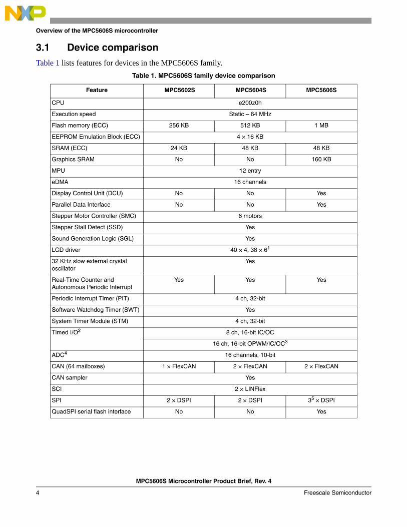
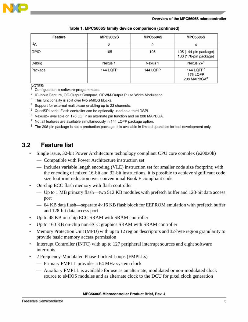
3.1 Device comparisonTable 1 lists features for devices in the MPC5606S family.
Table 1. MPC5606S family device comparison
Feature MPC5602S MPC5604S MPC5606S
CPU e200z0h
Execution speed Static – 64 MHz
Flash memory (ECC) 256 KB 512 KB 1 MB
EEPROM Emulation Block (ECC) 4 × 16 KB
SRAM (ECC) 24 KB 48 KB 48 KB
Graphics SRAM No No 160 KB
MPU 12 entry
eDMA 16 channels
Display Control Unit (DCU) No No Yes
Parallel Data Interface No No Yes
Stepper Motor Controller (SMC) 6 motors
Stepper Stall Detect (SSD) Yes
Sound Generation Logic (SGL) Yes
LCD driver 40 × 4, 38 × 61
32 KHz slow external crystal oscillator
Yes
Real-Time Counter and Autonomous Periodic Interrupt
Yes Yes Yes
Periodic Interrupt Timer (PIT) 4 ch, 32-bit
Software Watchdog Timer (SWT) Yes
System Timer Module (STM) 4 ch, 32-bit
Timed I/O2 8 ch, 16-bit IC/OC
16 ch, 16-bit OPWM/IC/OC3
ADC4 16 channels, 10-bit
CAN (64 mailboxes) 1 × FlexCAN 2 × FlexCAN 2 × FlexCAN
CAN sampler Yes
SCI 2 × LINFlex
SPI 2 × DSPI 2 × DSPI 35 × DSPI
QuadSPI serial flash interface No No Yes
MPC5606S Microcontroller Product Brief, Rev. 4
Freescale Semiconductor4
Overview of the MPC5606S microcontroller
3.2 Feature list• Single issue, 32-bit Power Architecture technology compliant CPU core complex (e200z0h)
— Compatible with Power Architecture instruction set
— Includes variable length encoding (VLE) instruction set for smaller code size footprint; with the encoding of mixed 16-bit and 32-bit instructions, it is possible to achieve significant code size footprint reduction over conventional Book E compliant code
• On-chip ECC flash memory with flash controller
— Up to 1 MB primary flash—two 512 KB modules with prefetch buffer and 128-bit data access port
— 64 KB data flash—separate 416 KB flash block for EEPROM emulation with prefetch buffer and 128-bit data access port
• Up to 48 KB on-chip ECC SRAM with SRAM controller
• Up to 160 KB on-chip non-ECC graphics SRAM with SRAM controller
• Memory Protection Unit (MPU) with up to 12 region descriptors and 32-byte region granularity to provide basic memory access permission
• Interrupt Controller (INTC) with up to 127 peripheral interrupt sources and eight software interrupts
• 2 Frequency-Modulated Phase-Locked Loops (FMPLLs)
— Primary FMPLL provides a 64 MHz system clock
— Auxiliary FMPLL is available for use as an alternate, modulated or non-modulated clock source to eMIOS modules and as alternate clock to the DCU for pixel clock generation
I2C 2 2 4
GPIO 105 105 105 (144-pin package)133 (176-pin package)
Debug Nexus 1 Nexus 1 Nexus 2+6
Package 144 LQFP 144 LQFP 144 LQFP7
176 LQFP208 MAPBGA8
NOTES:1 Configuration is software-programmable.2 IC-Input Capture, OC-Output Compare, OPWM-Output Pulse Width Modulation.3 This functionality is split over two eMIOS blocks.4 Support for external multiplexer enabling up to 23 channels.5 QuadSPI serial Flash controller can be optionally used as a third DSPI.6 Nexus2+ available on 176 LQFP as alternate pin function and on 208 MAPBGA.7 Not all features are available simultaneously in 144 LQFP package option.8 The 208-pin package is not a production package; it is available in limited quantities for tool development only.
Table 1. MPC5606S family device comparison (continued)
Feature MPC5602S MPC5604S MPC5606S
MPC5606S Microcontroller Product Brief, Rev. 4
Freescale Semiconductor 5
Overview of the MPC5606S microcontroller
• Crossbar switch architecture enables concurrent access of peripherals, flash memory or RAM from multiple bus masters (AMBA 2.0 v6 AHB)
• 16-channel Enhanced Direct Memory Access controller (eDMA) with multiple transfer request sources using a DMA channel multiplexer
• Boot Assist Module (BAM) supports internal flash programming via a serial link (FlexCAN or LINFlex)
• Display Control Unit to drive TFT LCD displays
— Includes processing of up to four planes that can be blended together
— Offers a direct unbuffered hardware bit-blitter of up to 16 software-configurable dynamic layers in order to drastically minimize graphic memory requirements and provide fast animations
— Programmable display resolutions are available up to WVGA
• Parallel Data Interface (PDI) for digital video input
• LCD segment driver module with two software programmable configurations:
— Up to 40 frontplane drivers and 4 backplane drivers
— Up to 38 frontplane drivers and 6 backplane drivers
• Stepper Motor Controller (SMC) module with high-current drivers for up to six instrument cluster gauges driven in full dual H-Bridge configuration including full diagnostics for short circuit detection
• Stepper motor return-to-zero and stall detection module
• Sound generation and playback utilizing PWM channels and eDMA; supports monotonic and polyphonic sound
• 24 eMIOS channels providing up to 16 PWM and 24 input capture / output compare channels
• 10-bit Analog-to-Digital Converter (ADC)
— Maximum conversion time of 1 s
— Up to 16 internal channels, expandable to 23 via external multiplexing
• Up to 2 Deserial Serial Peripheral Interface (DSPI) modules for full-duplex, synchronous, communications with external devices (extendable to include up to 8 multiplexed external channels)
• QuadSPI serial flash memory controller supporting single, dual and quad modes of operation to interface to external serial flash memory. QuadSPI can be configured to function as another DSPI module (MPC5606S only).
• 2 Local Interconnect Network Flexible (LINFlex) controller modules capable of autonomous message handling (master), autonomous header handling (slave mode), and UART support. Compliant with LIN protocol rev 2.1
• 2 full CAN 2.0B controllers with 64 configurable buffers each; bit rate programmable up to 1 Mbit/s
• Up to 4 Inter-integrated circuit (I2C) internal bus controllers with master/slave bus interface
• Up to 133 configurable general purpose pins supporting input and output operations
• Real Time Counter (RTC) with multiple clock sources:
MPC5606S Microcontroller Product Brief, Rev. 4
Freescale Semiconductor6
Overview of the MPC5606S microcontroller
— 128 kHz slow internal RC oscillator or 16 MHz fast internal RC oscillator supporting autonomous wakeup with 1 ms resolution with maximum timeout of 2 seconds
— 32 KHz slow external crystal oscillator, supporting wakeup with 1 s resolution and maximum timeout of one hour
— 4–16 MHz fast external crystal oscillator
• System timers:
— 4-channel 32-bit System Timer Module (STM)—included in processor platform
— 4-channel 32-bit Periodic Interrupt Timer (PIT) module
— Software Watchdog Timer (SWT)
• System Integration Unit (SIU) module to manage resets, external interrupts, GPIO and pad control
• System Status and Configuration Module (SSCM) to provide information for identification of the device, last boot mode, or debug status and provides an entry point for the censorship password mechanism
• Clock Generation Module (MC_CGM) to generate system clock sources and provide a unified register interface, enabling access to all clock sources
• Clock Monitor Unit (CMU) to monitor the integrity of the main crystal oscillator and the PLL and act as a frequency meter, measuring the frequency of one clock source and comparing it to a reference clock
• Mode Entry Module (MC_ME) to control the device power mode, i.e., RUN, HALT, STOP, or STANDBY, control mode transition sequences, and manage the power control, voltage regulator, clock generation and clock management modules
• Reset Generation Module (MC_RGM) to manage reset assertion and release to the device at initial power-up
• Nexus development interface (NDI) per IEEE-ISTO 5001-2003 Class Two Plus standard
• Device/board boundary-scan testing supported per Joint Test Action Group (JTAG) of IEEE (IEEE 1149.1)
• On-chip voltage regulator controller for regulating the 3.3 or 5 V supply voltage down to 1.2 V for core logic (requires external ballast transistor)
• The MPC5606S microcontrollers are offered in the following packages:1
— 144 LQFP, 0.5 mm pitch, 20 mm 20 mm outline
— 176 LQFP, 0.5 mm pitch, 24 mm 24 mm outline
— 208 MAPBGA, 1.0 mm pitch, 17 mm 17 mm outline (not a production package; available in limited quantities for tool development only)
1. See the device comparison table or orderable parts summary for package offerings for each device in the family.
MPC5606S Microcontroller Product Brief, Rev. 4
Freescale Semiconductor 7
Overview of the MPC5606S microcontroller
3.3 Feature details
3.3.1 Low-power operation
MPC5606S devices are designed for optimized low-power operation and dynamic power management of the core processor and peripherals. Power management features include software-controlled clock gating of peripherals and multiple power domains to minimize leakage in low-power modes.
There are two static low-power modes, STANDBY and STOP, and six dynamic power modes—five RUN modes and HALT. Both low power modes use clock gating to halt the clock for all or part of the device. The STANDBY mode also uses power gating to automatically turn off the power supply to parts of the device to minimize leakage.
STANDBY mode turns off the power to the majority of the chip to offer the lowest power consumption mode. The contents of the cores, on-chip peripheral registers and potentially some of the volatile memory are lost. STANDBY mode is configurable to make certain features available with the disadvantage that these consume additional current:
• It is possible to retain the contents of the full RAM or only 8 KB.
• It is possible to enable the internal 16 MHz or 128 kHz RC oscillator, the external 4–16 MHz oscillator, or the external 32 KHz oscillator.
• It is possible to keep the LCD module active.
The device can be awakened from STANDBY mode via from any of up to 19 I/O pins, a reset or from a periodic wake-up using a low power oscillator.
STOP mode maintains power to the entire device allowing the retention of all on-chip registers and memory, and providing a faster recovery low power mode than the lowest STANDBY mode. There is no need to reconfigure the device before executing code. The clocks to the core and peripherals are halted and can be optionally stopped to the oscillator or PLL at the expense of a slower start-up time.
STOP is entered from RUN mode only. Wake-up from STOP mode is triggered by an external event or by the internal periodic wake-up, if enabled.
RUN modes are the main operating mode where the entire device can be powered and clocked and from which most processing activity is done. One default (DRUN) and four dynamic RUN modes are supported—RUN0 - RUN3. The ability to configure and select different RUN modes enables different clocks and power configurations to be supported with respect to each other and to allow switching between different operating conditions. The necessary peripherals, clock sources, clock speed and system clock prescalers can be independently configured for each of the four RUN modes of the device.
HALT mode is a reduced activity, low power mode intended for moderate periods of lower processing activity. In this mode the core system clocks are stopped but user-selected peripheral tasks can continue to run. It can be configured to provide more efficient power management features (switch-off PLL, flash memory, main regulator, etc.) at the cost of longer wake up latency. The system returns to a RUN mode as soon as an event or interrupt is pending.
MPC5606S Microcontroller Product Brief, Rev. 4
Freescale Semiconductor8
Overview
of th
e MP
C5606S
micro
con
troller
9
POR
—
—
—
4 —
—
—
—
—
—
—
—
—
—
—
250 µs6
8 µs
s 100 µs
s 1 ms
s 200 µs
—
s BAM
MP
C5606S
Micro
con
troller P
rod
uct B
rief, Rev. 4
Freescale S
emiconductor
Table 2 summarizes the operating modes of MPC5606S devices.
Table 2. Operating mode summary1
Operating modes: RUN HALT STOP STANDBY
SoC features Core On CG CG Off Off
Peripherals OP OP CG Off2 Off
Flash memory OP OP CG Off Off
SRAM On On CG CG3 8 KB
Graphics RAM On On CG Off Off
Clock sources Main PLL OP OP CG Off Off
Auxiliary PLL OP OP CG Off Off
16 MHz IRC On On OP OP OP
X OSC OP OP OP OP OP
128 kHz IRC On On On On On
32 KHz XOSC OP OP OP OP OP
Periodic Wake-up — OP OP OP OP
Wake-up input — OP OP OP OP
VREG mode FP FP LP LP LP
Wakeup times5 VREG start-up — — 50 s 250 µs 50 µs
IRC wake-up — — 4 µs 4 µs 8 µs
Flash memory recovery
— — 20 µs 100 µs 100 µ
OSC stabilization — — 1 ms 1 ms 1 m
PLL lock — — 200 µs 200 µs 200 µ
S/W reconfig — — — Var Var
Mode switch over — 200.69 µs 24 µs 28 µs 28 µ
Overview of the MPC5606S microcontroller
Additional notes on low power operation:
• Fast wake-up using the on-chip 16 MHz internal RC oscillator allows rapid execution from RAM on exit from low power modes
• The 16 MHz internal RC oscillator supports low speed code execution and clocking of peripherals when it is selected as the system clock and can also be used as the PLL input clock source to provide fast start-up without the external oscillator delay
• MPC5606S devices include an internal voltage regulator that includes the following features:
— Regulates input to generate all internal supplies
— Manages power gating
— Low power regulators support operation when in STOP and STANDBY modes to minimize power consumption
— Startup on-chip regulators in <50 s for rapid exit of STOP and STANDBY modes
— Low voltage detection on main supply and 1.2 V regulated supplies
3.3.2 e200z0h core processor
The e200z0h processor is similar to other processors in the e200zx series but supports only the VLE instruction set and does not include the signal processing extension for DSP applications or a floating point unit.
The e200z0h has all the features of the e200z0 plus:
• Branch acceleration using Branch Target Buffer (BTB)
• Supports independent instruction and data accesses to different memory subsystems, such as SRAM and Flash memory via independent Instruction and Data BIUs
NOTES:1 Table Key:
On- Powered and clocked
OP- Optionally configurable to be enabled or disabled (clock gated)
CG- Clock Gated, Powered but clock stoppedOff- Powered off and clock gated
FP- VREG Full Performance mode
LP- VREG Low Power mode, reduced output capability of VREG but lower power consumption
Var- Variable duration, based on the required reconfiguration and execution clock speedBAM- Boot Assist Module Software and Hardware used for device start-up and configuration
2 The LCD can optionally be kept running while the device is in STANDBY mode3 All of the RAM content is retained, but not accessible in STANDBY mode4 8 KB of the RAM content is retained, but not accessible in STANDBY mode5 A high level summary of some key durations that need to be considered when recovering from low power modes.
This does not account for all durations at wake up. Other delays will be necessary to consider including, but not limited to the external supply start-up time. IRC Wake-up time must not be added to the overall wake-up time as it starts in parallel with the VREG.All other wake-up times must be added to determine the total start-up time
6 This is the startup of the regulator that happens after the 5 V has reached beyond its POR range. If the external supply ramp rate is slow, measure from when VREG has crossed beyond the POR threshold, otherwise this value will depend on the ramp rate of the external supply (VDDR).
MPC5606S Microcontroller Product Brief, Rev. 4
Freescale Semiconductor10
Overview of the MPC5606S microcontroller
The e200z0h processor uses a four stage in-order pipeline for instruction execution. The Instruction Fetch (stage 1), Instruction Decode/Register file Read/Effective Address Calculation (stage 2), Execute/Memory Access (stage 3), and Register Writeback (stage 4) stages operate in an overlapped fashion, allowing single clock instruction execution for most instructions.
The integer execution unit consists of a 32-bit Arithmetic Unit (AU), a Logic Unit (LU), a 32-bit Barrel shifter (Shifter), a Mask-Insertion Unit (MIU), a Condition Register manipulation Unit (CRU), a Count-Leading-Zeros unit (CLZ), an 832 Hardware Multiplier array, result feed-forward hardware, and a hardware divider.
Most arithmetic and logical operations are executed in a single cycle with the exception of the divide and multiply instructions. A Count-Leading-Zeros unit operates in a single clock cycle. The Instruction Unit contains a PC incrementer and a dedicated Branch Address adder to minimize delays during change of flow operations. Branch target prefetching from the BTB is performed to accelerate certain taken branches. Sequential prefetching is performed to ensure a supply of instructions into the execution pipeline. Branch target prefetching is performed to accelerate taken branches. Prefetched instructions are placed into an instruction buffer capable of holding four instructions.
Conditional branches not taken execute in a single clock. Branches with successful target prefetching have an effective execution time of one clock on e200z0h. All other taken branches have an execution time of two clocks.
Memory load and store operations are provided for byte, halfword, and word (32-bit) data with automatic zero or sign extension of byte and halfword load data as well as optional byte reversal of data. These instructions can be pipelined to allow effective single cycle throughput. Load and store multiple word instructions allow low overhead context save and restore operations. The load/store unit contains a dedicated effective address adder to allow effective address generation to be optimized. Also, a load-to-use dependency does not incur any pipeline bubbles for most cases.
The Condition Register unit supports the condition register (CR) and condition register operations defined by the Power Architecture. The condition register consists of eight 4-bit fields that reflect the results of certain operations, such as move, integer and floating-point compare, arithmetic, and logical instructions, and provide a mechanism for testing and branching.
Vectored and autovectored interrupts are supported. Hardware vectored interrupt support is provided to allow multiple interrupt sources to have unique interrupt handlers invoked with no software overhead.
The CPU includes support for Variable Length Encoding (VLE) instruction enhancements. This allows the Power Architecture instruction set to be represented by a modified instruction set made up from a mixture of 16-bit and 32-bit instructions. This results in a significantly smaller code size footprint without affecting performance noticeably.
The CPU core is enhanced by an additional interrupt source—Non Maskable Interrupt. This interrupt source is routed directly from package pins, via edge detection logic in the SIU to the CPU, bypassing the Interrupt Controller completely. Once the edge detection logic is programmed, it can not be disabled, except by reset. The Non Maskable Interrupt is, as the name suggests, completely un-maskable and when asserted will always result in the immediate execution of the respective interrupt service routine. The Non maskable interrupt is not guaranteed to be recoverable.
MPC5606S Microcontroller Product Brief, Rev. 4
Freescale Semiconductor 11
Overview of the MPC5606S microcontroller
The CPU core has an additional ‘Wait for Interrupt’ instruction that is used in conjunction with low power STOP mode. When Low Power Stop mode is selected, this instruction is executed to allow the system clock to be stopped. An external interrupt source or the system wake-up timer is used to restart the system clock and allow the CPU to service the interrupt.
Additional features include:
• Load/store unit
— 1-cycle load latency
— Misaligned access support
— No load-to-use pipeline bubbles
• Thirty-two 32-bit general purpose registers (GPRs)
• Separate instruction bus and load/store bus Harvard architecture
• Reservation instructions for implementing read-modify-write constructs
• Multi-cycle divide (divw) and load multiple (lmw) store multiple (smw) multiple class instructions, can be interrupted to prevent increases in interrupt latency
• Extensive system development support through Nexus debug port
3.3.3 Crossbar switch (XBAR)
The XBAR multi-port crossbar switch supports simultaneous connections between four master ports and four slave ports. The crossbar supports a 32-bit address bus width and a 32-bit data bus width.
The crossbar allows four concurrent transactions to occur from any master port to any slave port but one of those transfers must be an instruction fetch from internal flash. If a slave port is simultaneously requested by more than one master port, arbitration logic selects the higher priority master and grants it ownership of the slave port. All other masters requesting that slave port are stalled until the higher priority master completes its transactions. Requesting masters having equal priority are granted access to a slave port in round-robin fashion, based upon the ID of the last master to be granted access.
The crossbar provides the following features:
• 4 master ports:
— e200z0h core instruction port
— e200z0h core complex load/store data port
— eDMA controller
— Display control unit
• 4 slave ports:
— 1 flash port dedicated to the CPU
— Platform SRAM
— QuadSPI serial flash controller
— 1 slave port combining:
– Flash port dedicated to the Display Control Unit and eDMA module
– Graphics SRAM
MPC5606S Microcontroller Product Brief, Rev. 4
Freescale Semiconductor12
Overview of the MPC5606S microcontroller
– Peripheral bridge
• 32-bit internal address bus, 32-bit internal data bus
3.3.4 Enhanced Direct Memory Access (eDMA)
The eDMA module is a controller capable of performing complex data movements via 16 programmable channels, with minimal intervention from the host processor. The hardware micro architecture includes a DMA engine which performs source and destination address calculations, and the actual data movement operations, along with an SRAM-based memory containing the transfer control descriptors (TCD) for the channels. This implementation is utilized to minimize the overall block size. The eDMA module provides the following features:
• 16 channels support independent 8-, 16- or 32-bit single value or block transfers
• Supports variable sized queues and circular queues
• Source and destination address registers are independently configured to post-increment or remain constant
• Each transfer is initiated by a peripheral, CPU, periodic timer interrupt or eDMA channel request
• Each DMA channel can optionally send an interrupt request to the CPU on completion of a single value or block transfer
• DMA transfers possible between system memories, QuadSPI, DSPIs, I2C, ADC, eMIOS and General Purpose I/Os (GPIOs)
• Programmable DMA Channel Mux allows assignment of any DMA source to any available DMA channel with up to a total of 64 potential request sources.
3.3.5 Inter-IC communications module (I2C)
The I2C module features the following:
• Up to four I2C modules supported
• Two-wire bi-directional serial bus for on-board communications
• Compatibility with I2C bus standard
• Multimaster operation
• Software-programmable for one of 256 different serial clock frequencies
• Software-selectable acknowledge bit
• Interrupt-driven, byte-by-byte data transfer
• Arbitration-lost interrupt with automatic mode switching from master to slave
• Calling address identification interrupt
• Start and stop signal generation/detection
• Repeated START signal generation
• Acknowledge bit generation/detection
• Bus-busy detection
MPC5606S Microcontroller Product Brief, Rev. 4
Freescale Semiconductor 13
Overview of the MPC5606S microcontroller
3.3.6 Interrupt Controller (INTC)
The INTC provides priority-based preemptive scheduling of interrupt requests, suitable for statically scheduled hard real-time systems.
For high priority interrupt requests, the time from the assertion of the interrupt request from the peripheral to when the processor is executing the interrupt service routine (ISR) has been minimized. The INTC provides a unique vector for each interrupt request source for quick determination of which ISR needs to be executed. It also provides an ample number of priorities so that lower priority ISRs do not delay the execution of higher priority ISRs. To allow the appropriate priorities for each source of interrupt request, the priority of each interrupt request is software configurable.
When multiple tasks share a resource, coherent accesses to that resource need to be supported. The INTC supports the priority ceiling protocol for coherent accesses. By providing a modifiable priority mask, the priority can be raised temporarily so that all tasks which share the resource can not preempt each other.
Multiple processors can assert interrupt requests to each other through software setable interrupt requests. These same software setable interrupt requests also can be used to break the work involved in servicing an interrupt request into a high priority portion and a low priority portion. The high priority portion is initiated by a peripheral interrupt request, but then the ISR asserts a software setable interrupt request to finish the servicing in a lower priority ISR. Therefore these software setable interrupt requests can be used instead of the peripheral ISR scheduling a task through the RTOS. The INTC provides the following features:
• Unique 9-bit vector for each of the possible 128 separate interrupt sources
• 8 software triggerable interrupt sources
• 16 priority levels with fixed hardware arbitration within priority levels for each interrupt source
• Ability to modify the ISR or task priority.
— Modifying the priority can be used to implement the Priority Ceiling Protocol for accessing shared resources.
• External non maskable interrupt directly accessing the main core critical interrupt mechanism
• 32 external interrupts
3.3.7 QuadSPI serial flash controller
The QuadSPI module enables use of external serial flash memories supporting single, dual and quad modes of operation. It features the following:
• Memory mapping of external serial flash
• Automatic serial flash read command generation by CPU, DMA or DCU read access on AHB bus
• Supports single, dual and quad serial flash read commands
• Flexible buffering scheme to maximize read bandwidth of serial flash
• ‘Legacy’ mode allowing QuadSPI to be used as a standard DSPI (no DSI or CSI mode)
MPC5606S Microcontroller Product Brief, Rev. 4
Freescale Semiconductor14
Overview of the MPC5606S microcontroller
3.3.8 System Integration Unit (SIU)
The SIU controls MCU reset configuration, pad configuration, external interrupt, general purpose I/O (GPIO), internal peripheral multiplexing, and the system reset operation.
The GPIO features the following:
• Up to 4 levels of internal pin multiplexing, allowing exceptional flexibility in the allocation of device functions for each package
• Centralized general purpose input output (GPIO) control of up to 132 input/output pins (package dependent)
• All GPIO pins can be independently configured to support pull-up, pull down, or no pull
• Reading and writing to GPIO supported both as individual pins and 16-bit wide ports
• All peripheral pins can be alternatively configured as both general purpose input or output pins except ADC channels which support alternative configuration as general purpose inputs
• Direct readback of the pin value supported on all digital output pins through the SIU
• Configurable digital input filter that can be applied to up to 14 general purpose input pins for noise elimination on external interrupts
• Register configuration protected against change with soft lock for temporary guard or hard lock to prevent modification until next reset.
3.3.9 Flash memory
The MPC5606S microcontroller has the following flash memory features:
• Up to 1 MB of burst flash memory
— Typical flash memory access time: 0 wait-state for buffer hits, 2 wait-states for page buffer miss at 64 MHz
— Two 4128-bit page buffers with programmable prefetch control
– 1 set of page buffers can be allocated for code-only, fixed partitions of code and data, all available for any access
– 1 set of page buffers allocated to Display Controller Unit and the eDMA
— 64-bit ECC with single-bit correction, double-bit detection for data integrity
— 64 KB data flash memory — separate 416 KB flash block for EEPROM emulation with prefetch buffer and 128-bit data access port
• Small block flash memory arrangement to support features such as boot block, operating system block
• Hardware managed flash memory writes, erase and verify sequence
• Censorship protection scheme to prevent flash memory content visibility
• Separate dedicated 64 KB data flash memory for EEPROM emulation
— 4 erase sectors each containing 16 KB of memory
— Offers Read-While-Write functionality from main program space
— Same data retention and program erase specification as main program flash memory array
MPC5606S Microcontroller Product Brief, Rev. 4
Freescale Semiconductor 15
Overview of the MPC5606S microcontroller
3.3.10 SRAM
The MPC5606S microcontrollers have up to 48 KB general-purpose on-chip SRAM with the following features:
• Typical SRAM access time: 0 wait-state for reads and 32-bit writes; 1 wait-state for 8- and 16-bit writes if back to back with a read to same memory block
• 32-bit ECC with single-bit correction, double bit detection for data integrity
• Supports byte (8-bit), half word (16-bit), and word (32-bit) writes for optimal use of memory
• User transparent ECC encoding and decoding for byte, half word, and word accesses
• Separate internal power domain applied to full SRAM block, 8 KB SRAM block during STANDBY modes to retain contents during low power mode.
3.3.11 On-chip graphics SRAM
The MPC5606S microcontroller has 160 KB on-chip graphics SRAM with the following features:
• Usable as general purpose SRAM
• Typical SRAM access time: 0 wait-state for reads and 32-bit writes
• Supports byte (8-bit), half word (16-bit), and word (32-bit) writes for optimal use of memory
3.3.12 Memory Protection Unit (MPU)
The MPU features the following:
• 12 region descriptors for per master protection
• Start and end address defined with 32-byte granularity
• Overlapping regions supported
• Protection attributes can optionally include process ID
• Protection offered for 3 concurrent read ports
• Read and write attributes for all masters
• Execute and supervisor/user mode attributes for processor masters
3.3.13 Boot Assist Module (BAM)
The BAM is a block of read-only memory that is programmed once by Freescale. The BAM program is executed every time the MCU is powered-on or reset in normal mode. The BAM supports different modes of booting. They are:
• Booting from internal flash memory
• Serial boot loading (A program is downloaded into RAM via FlexCAN or LINFlex and then executed)
• Booting from external memory
Additionally the BAM:
• Enables and manages the transition of the MCU from reset to user code execution
MPC5606S Microcontroller Product Brief, Rev. 4
Freescale Semiconductor16
Overview of the MPC5606S microcontroller
• Configures device for serial bootload
• Enables multiple bootcode starting locations out of reset through implementation of search for valid Reset Configuration Halfword
• Enables or disables software watchdog timer out of reset through BAM read of Reset Configuration Halfword option bit
3.3.14 Enhanced Modular Input/Output System (eMIOS)
MPC5606S microcontrollers have two eMIOS modules—one with 16 channels and one with 8—with input/output channels supporting a range of 16-bit input capture, output compare, and Pulse Width Modulation functions.
The modules are configurable and can implement 8-channel, 16-bit input capture/output compare or 16-channel, 16-bit output pulse width modulation/input compare/output compare. Up to five additional channels are configurable as modulus counters.
eMIOS other features include:
• Selectable clock source from main FMPLL, auxiliary FMPLL, external 4–16 MHz oscillator or 16 MHz Internal RC oscillator
• Timed I/O channels with 16-bit counter resolution
• Buffered updates
• Support for shifted PWM outputs to minimize occurrence of concurrent edges
• Edge aligned output pulse width modulation
— Programmable pulse period and duty cycle
— Supports 0% and 100% duty cycle
— Shared or independent time bases
• Programmable phase shift between channels
• Selectable combination of pairs of eMIOS outputs to support sound generation
• DMA transfer support
• Selectable clock source from the primary FMPLL, auxiliary FMPLL, external 4–16 MHz oscillator or the 16 MHz internal RC oscillator.
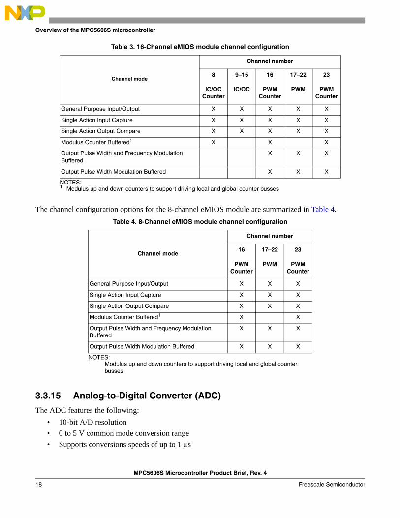
The channel configuration options for the 16-channel eMIOS module are summarized in Table 3.
MPC5606S Microcontroller Product Brief, Rev. 4
Freescale Semiconductor 17
Overview of the MPC5606S microcontroller
The channel configuration options for the 8-channel eMIOS module are summarized in Table 4.
3.3.15 Analog-to-Digital Converter (ADC)
The ADC features the following:
• 10-bit A/D resolution
• 0 to 5 V common mode conversion range
• Supports conversions speeds of up to 1 s
Table 3. 16-Channel eMIOS module channel configuration
Channel mode
Channel number
8
IC/OCCounter
9–15
IC/OC
16
PWMCounter
17–22
PWM
23
PWMCounter
General Purpose Input/Output X X X X X
Single Action Input Capture X X X X X
Single Action Output Compare X X X X X
Modulus Counter Buffered1
NOTES:1 Modulus up and down counters to support driving local and global counter busses
X X X
Output Pulse Width and Frequency Modulation Buffered
X X X
Output Pulse Width Modulation Buffered X X X
Table 4. 8-Channel eMIOS module channel configuration
Channel mode
Channel number
16
PWMCounter
17–22
PWM
23
PWMCounter
General Purpose Input/Output X X X
Single Action Input Capture X X X
Single Action Output Compare X X X
Modulus Counter Buffered1
NOTES:1 Modulus up and down counters to support driving local and global counter
busses
X X
Output Pulse Width and Frequency Modulation Buffered
X X X
Output Pulse Width Modulation Buffered X X X
MPC5606S Microcontroller Product Brief, Rev. 4
Freescale Semiconductor18
Overview of the MPC5606S microcontroller
• 16 internal and 8 external channels support
• Up to 16 single-ended inputs channels
— All channels configured to have alternate function as general purpose input/output pins
– 10-bit ± 3 counts accuracy (TUE)
• External multiplexer support to increase up to 23 channels
— Automatic 1 × 8 multiplexer control
— External multiplexer connected to a dedicated input channel
— Shared register between the 8 external channels
• Result register available for every non-multiplexed channel
• Configurable Left or Right aligned result format
• Supports for one-shot, scan and injection conversion modes
• Injection mode status bit implemented on adjacent 16-bit register for each result
— Supports Access to Result and injection status with single 32-bit read
• Independently enabling of function for channels:
— Offset Refresh
• Conversion Triggering support
— Internal conversion triggering from periodic interrupt timer (PIT)
• 4 configurable analog comparator channels offering range comparison with triggered alarm
— Greater than
— Less than
— Out of range
• All unused analog inputs can be used as general purpose input and output pins
• Power Down mode
• Optional support for DMA transfer of results
3.3.16 Deserial Serial Peripheral Interface (DSPI)
The deserial serial peripheral interface (DSPI) modules provide a synchronous serial interface for communication between the MPC5606S MCU and external devices.
The DSPI features the following:
• Up to two DSPI modules
• Full duplex, synchronous transfers
• Master or slave operation
• Programmable master bit rates
• Programmable clock polarity and phase
• End-of-transmission interrupt flag
• Programmable transfer baud rate
• Programmable data frames from 4 to 16 bits
MPC5606S Microcontroller Product Brief, Rev. 4
Freescale Semiconductor 19
Overview of the MPC5606S microcontroller
• Up to 6 chip select lines available, depending on package and pin multiplexing, enable 64 external devices to be selected using external muxing from a single DSPI
• 8 clock and transfer attributes registers
• Chip select strobe available as alternate function on one of the chip select pins for deglitching
• FIFOs for buffering up to 4 transfers on the transmit and receive side
• General purpose I/O functionality on pins when not used for SPI
• Queueing operation possible through use of eDMA
3.3.17 FlexCAN
The MPC5606S MCU contains two controller area network (FlexCAN) modules. The FlexCAN module is a communication controller implementing the CAN protocol according to Bosch Specification version 2.0B. The CAN protocol was designed to be used primarily as a vehicle serial data bus, meeting the specific requirements of this field: real-time processing, reliable operation in the EMI environment of a vehicle, cost-effectiveness and required bandwidth.
The FlexCan modules offer the following:
• Compliant with CAN protocol specification, Version 2.0B active
• 64 mailboxes, each configurable as transmit or receive
— Mailboxes configurable while module remains synchronized to CAN bus
• Transmit features
— Supports configuration of multiple mailboxes to form message queues of scalable depth
— Arbitration scheme according to message ID or message buffer number
— Internal arbitration to guarantee no inner or outer priority inversion
— Transmit abort procedure and notification
• Receive features
— Individual programmable filters for each mailbox
— 8 mailboxes configurable as a 6-entry receive FIFO
— 8 programmable acceptance filters for receive FIFO
• Programmable clock source
— System clock
— Direct oscillator clock to avoid PLL jitter
• Listen only mode capabilities
• CAN Sampler
— Can catch the 1st message sent on the CAN network while the MPC5606S is stopped. This guarantees a clean startup of the system without missing messages on the CAN network.
— The CAN sampler is connected to one of the CAN RX pins.
MPC5606S Microcontroller Product Brief, Rev. 4
Freescale Semiconductor20
Overview of the MPC5606S microcontroller
3.3.18 Serial communication interface module (LINFlex)
The MPC5606S devices include up to two LINFlex modules and support for LIN Master mode, LIN Slave mode and UART mode. The modules are LIN state machine compliant to the LIN 1.3 and 2.0 and 2.1 Specifications and handle LIN frame transmission and reception without CPU intervention.
Other features include:
• Autonomous LIN frame handling
• Message buffer to store identifier and up to eight data bytes
• Supports message length of up to 64 bytes
• Detection and flagging of LIN errors
• Sync field; Delimiter; ID parity; Bit, Framing; Checksum and Timeout errors
• Classic or extended checksum calculation
• Configurable Break duration of up to 36-bit times
• Programmable Baud rate prescalers (13-bit mantissa, 4-bit fractional)
• Diagnostic features
— Loop back
— Self Test
— LIN bus stuck dominant detection
• Interrupt driven operation with 16 interrupt sources
• LIN slave mode features
— Autonomous LIN header handling
— Autonomous LIN response handling
— Discarding of irrelevant LIN responses using up to 16 ID filters
• UART mode
— Full-duplex operation
— Standard non return-to-zero (NRZ) mark/space format
— Data buffers with 4-byte receive, 4-byte transmit
— Configurable word length (8-bit or 9-bit words)
— Error detection and flagging
– Parity, noise and framing errors
— Interrupt driven operation with 4 interrupts sources
— Separate transmitter and receiver CPU interrupt sources
— 16-bit programmable baud-rate modulus counter and 16-bit fractional
— 2 receiver wake-up methods
3.3.19 System clocks and clock generation modules
The system clock on the MPC5606S can be derived from an external oscillator, an on-chip FMPLL, or the internal 16 MHz oscillator.
MPC5606S Microcontroller Product Brief, Rev. 4
Freescale Semiconductor 21
Overview of the MPC5606S microcontroller
• The source system clock frequency can be changed via an on-chip programmable clock divider (1 to 2).
• Additional programmable peripheral bus clock divider ratio (1 to 16)
• The MPC5606S has 2 on-chip FMPLLs—the primary module and an auxiliary module.
— Each features the following:
– Input clock frequency from 4 MHz to 16 MHz
– Lock detect circuitry continuously monitors lock status
– Loss Of Clock (LOC) detection for reference and feedback clocks
– On-chip loop filter (for improved electromagnetic interference performance and reduction of number of external components required)
– Support for frequency ramping from PLL
— The primary FMPLL module is for use as a system clock source. The auxiliary FMPLL is available for use as an alternate, modulated or non-modulated clock source to eMIOS modules and as alternate clock to the DCU for pixel clock generation.
• The main oscillator provides the following features:
— Input frequency range 4–16 MHz
— Square-wave input mode
— Oscillator input mode 3.3 V (5.0 V)
— Automatic level control
— PLL reference
• MPC5606S includes a 32 KHz low power external oscillator for slow execution, low power, and Real Time Clock
• Dedicated internal 128 kHz RC oscillator for low power mode operation and self wake-up
— ±10% accuracy across voltage and temperature (after factory trimming)
— Trimming registers to support improved accuracy with in-application calibration
• Dedicated 16 MHz internal RC oscillator
— Used as default clock source out of reset
— Provides a clock for rapid start-up from low power modes
— Provides a back-up clock in the event of PLL or External Oscillator clock failure
— Offers an independent clock source for the Watchdog timer
— ±5% accuracy across voltage and temperature (after factory trimming)
— Trimming registers to support frequency adjustment with in-application calibration
3.3.20 Periodic Interrupt Timer module (PIT)
The PIT features the following:
• 4 general purpose interrupt timers
• Up to 2 dedicated interrupt timers for triggering ADC conversions
• 32-bit counter resolution
MPC5606S Microcontroller Product Brief, Rev. 4
Freescale Semiconductor22
Overview of the MPC5606S microcontroller
• Clocked by system clock frequency
• 32-bit counter for Real Time Interrupt, clocked from main external oscillator
3.3.21 Real Time Counter (RTC)
Real Timer Counter supports wake-up from Low Power modes or Real Time Clock generation
• Configurable resolution for different timeout periods
— 1 s resolution for >1 hour period
— 1 ms resolution for 2 second period
• Selectable clock sources from external 32 KHz crystal, external 4–16 MHz crystal, internal 128 kHz RC oscillator or divided internal 16 MHz RC oscillator
3.3.22 System Timer Module (STM)
The STM is a 32-bit timer designed to support commonly required system and application software timing functions. The STM includes a 32-bit up counter and four 32-bit compare channels with a separate interrupt source for each channel. The counter is driven by the system clock divided by an 8-bit prescale value (1 to 256).
• One 32-bit up counter with 8-bit prescaler
• Four 32-bit compare channels
• Independent interrupt source for each channel
• Counter can be stopped in debug mode
3.3.23 Software Watchdog Timer (SWT)
The Watchdog features the following:
• Watchdog supporting software activation or enabled out of Reset
• Supports normal or windowed mode
• Watchdog timer value writable once after reset
• Watchdog supports optional halting during low power modes
• Configurable response on timeout: reset, interrupt, or interrupt followed by reset
• Selectable clock source for main system clock or internal 16 MHz RC oscillator clock
3.3.24 Display Control Unit (DCU)
The DCU is a display controller designed to drive TFT LCD displays capable of driving up to WVGA resolution screens with 16 layers and 4 planes with real time alpha-blending.
The DCU generates all the necessary signals required to drive the display: up to 24-bit RGB data bus, Pixel Clock, Data Enable, Horizontal-Sync and Vertical-Sync.
The internal memory resources of the Spectrum allow the display of complex graphics contents (pictures, icons, languages, fonts) on a color TFT panel in up to Wide Quarter Video Graphics Array (WQVGA)
MPC5606S Microcontroller Product Brief, Rev. 4
Freescale Semiconductor 23
Overview of the MPC5606S microcontroller
sizes. All the data fetches from internal and/or external memory are performed by the internal four-channel DMA of the DCU providing a high speed/low latency access to the system backbone.
Control Descriptors (CDs) associated with each layer enable effective merging of different color formats into one plane to optimize use of internal memory buffers. A layer may be constructed from graphic content of various color formats including 1bpp, 2bpp, 4bpp, 8bpp, 16bpp, 24bpp and 24bpp+alpha. The ability of the DCU to handle input data in formats as low as 1bpp, 2bpp and 4bpp enables a highly efficient use of internal memory resources of the MPC5606S. A special tiled mode can be enabled on any of the 16 layers to repeat a pattern optimizing graphic memory usage.
A hardware cursor can be managed independently of the layers at blending level increasing the efficient use of the internal DCU resources.
To secure the content of all critical information to be displayed, a safety mode can be activated to check the integrity of critical data along the whole system data path from the memory to the TFT pads.
The DCU features the following:
• Display color depth: up to 24 bpp
• Generation of all RGB and control signals for TFT
• Four-layer blending at each pixel position
• Maximum number of Input Layers: 16 (fixed priority)
• Dynamic Look-Up-Table (Color and Gamma Look-Up)
• blending range: up to 256 levels
• Transparency Mode for font or single foreground color graphics
• Gamma Correction
• Tiled mode on all the layers
• Hardware Cursor
• Critical display content integrity monitoring for Functional Safety support
• Internal Direct Memory Access (DMA) module to transfer data from internal and / or external memory.
3.3.25 Parallel Data Interface (PDI)
The PDI is a digital interface used to receive external digital video or graphic content into the DCU.
The PDI input is directly injected into the DCU background plane FIFO. When the PDI is activated, all the DCU synchronization is extracted from the external video stream to guarantee the synchronization of the two video sources.
The PDI can be used to:
• Connect a Video Camera output directly to the PDI
• Connect a secondary display driver as slave with a minimum of extra cost
• Connect a device gathering various Video sources
• Provide flexibility to allow the DCU to be used in slave mode (external synchronization)
MPC5606S Microcontroller Product Brief, Rev. 4
Freescale Semiconductor24
Overview of the MPC5606S microcontroller
The PDI features the following:
• Supported color modes:
— 8-bit mono
— 8-bit color multiplexed
— RGB565
— 16-bit/18-bit RAW color
• Supported synchronization modes:
— Embedded ITU-R BT.656-4 (RGB565 mode 2)
— HSYNC, VSYNC
— Data Enable
• Direct interface with DCU background plane FIFO
• Synchronization generation for the DCU
3.3.26 Liquid Crystal Display (LCD) driver
The LCD driver module has two configurations allowing a maximum of 160 or 228 LCD segments:
• Up to 40 frontplane drivers and 4 backplane drivers
• Up to 38 frontplane drivers and 6 backplane drivers
Each segment is controlled and can be masked by a corresponding bit in the LCD RAM.
Four to six multiplex modes (1/1, 1/2, 1/3, 1/4, 1/5, 1/6 duty), and three bias (1/1, 1/2, 1/3) methods are available. All frontplane and backplane pins can be multiplexed with other port functions.
The LCD driver module features the following:
• Programmable frame clock generator from different clock sources:
— System clock
— Internal RC oscillator
• Programmable bias voltage level selector
• On-chip generation of all output voltage levels
— LCD voltage reference taken from main 5V supply
• LCD RAM – contains the data to be displayed on the LCD
— Data can be read from or written to the display RAM at any time
• End of Frame interrupt:
— To optimize the refresh of the data without visual artefact
— Selectable number of frames between each interrupt
• Contrast adjustment using programmable internal voltage reference
• Remapping capability of 4 or 6 backplanes with frontplanes;
— To increase pin selection flexibility
MPC5606S Microcontroller Product Brief, Rev. 4
Freescale Semiconductor 25
Overview of the MPC5606S microcontroller
• In low power modes, the LCD operation can be suspended under software control. The LCD can also operate in low power modes, clocked by the internal 128 kHz IRC or external 32 KHz crystal oscillator
• Selectable output current boost during transitions
3.3.27 Stepper Motor Controller (SMC)
The SMC module is a PWM motor controller suitable to drive instruments in a cluster configuration or any other loads requiring a PWM signal. The motor controller has twelve PWM channels associated with two pins each (24 pins in total).
The SMC module includes the following features:
• 10/11-bit PWM counter
• 11-bit resolution with selectable PWM dithering function
• Left, right, or center aligned PWM
• Output slew rate control
• Output Short Circuit Detection
This module is suited for, but not limited to, driving small stepper and air core motors used in instrumentation applications. This module can be used for other motor control or PWM applications that match the frequency, resolution, and output drive capabilities of the module.
3.3.28 Stepper Stall Detect (SSD)
The stepper stall detector (SSD) module provides a circuit to measure and integrate the induced voltage on the non-driven coil of a stepper motor using full steps when the gauge pointer is returning to zero (RTZ).
The SSD module features the following:
• Programmable full step state
• Programmable integration polarity
• Blanking (recirculation) state
• 16-bit integration accumulator register
• 16-bit modulus down counter with interrupt
3.3.29 Sound Generation Logic (SGL)
The SGL has two modes of operation:
• Amplitude modulated PWM mode for low cost buzzers using any two eMIOS channels:
— Monophonic signal with amplitude control
— 8-bit amplitude resolution
— Ability to mix any two eMIOS channels.
— Requires simple external RC lowpass filter
• Digital sample mode for higher quality sound using one eMIOS channel and eDMA
MPC5606S Microcontroller Product Brief, Rev. 4
Freescale Semiconductor26
Application examples
— Up to 10-bit audio amplitude resolution
— Polyphonic sound synthesis
— Playback of sample based waveforms
— Text-to-speech possibility
— Requires external lowpass filter
3.3.30 IEEE 1149.1 JTAG Controller (JTAGC)
JTAGC features the following:
• Backward compatible to standard JTAG IEEE 1149.1-2001 test access port (TAP) interface
• Support for boundary scan testing
3.3.31 Nexus Development Interface (NDI)
Nexus features the following:
• Per IEEE-ISTO 5001-2003
• Nexus 2 Plus features supported
— Static debug
— Watchpoint messaging
— Ownership trace messaging
— Program trace messaging
— Real time read/write of any internally memory mapped resources through JTAG pins
— Overrun control, which selects whether to stall before Nexus overruns or keep executing and allow overwrite of information
— Watchpoint triggering, watchpoint triggers program tracing
• Configured via the IEEE 1149.1 (JTAG) port
• Nexus Auxiliary port supported on the 176 LQFP and 208-pin BGA package FOR DEVELOPMENT ONLY
— Narrow Auxiliary Nexus port supporting support trace, with 2 MDO pins
— Wide Auxiliary Nexus port supporting higher bandwidth trace, with 4 MDO pins
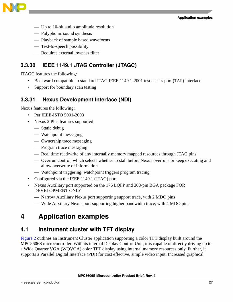
4 Application examples
4.1 Instrument cluster with TFT displayFigure 2 outlines an Instrument Cluster application supporting a color TFT display built around the MPC5606S microcontroller. With its internal Display Control Unit, it is capable of directly driving up to a Wide Quarter VGA (WQVGA) color TFT display using internal memory resources only. Further, it supports a Parallel Digital Interface (PDI) for cost effective, simple video input. Increased graphical
MPC5606S Microcontroller Product Brief, Rev. 4
Freescale Semiconductor 27
Application examples
content can be achieved using external serial flash memory and can be further extended with external flash and/or SRAM connected to the serial peripheral interface (QuadSPI).
Figure 2. Instrument cluster using the MPC5606S microcontroller
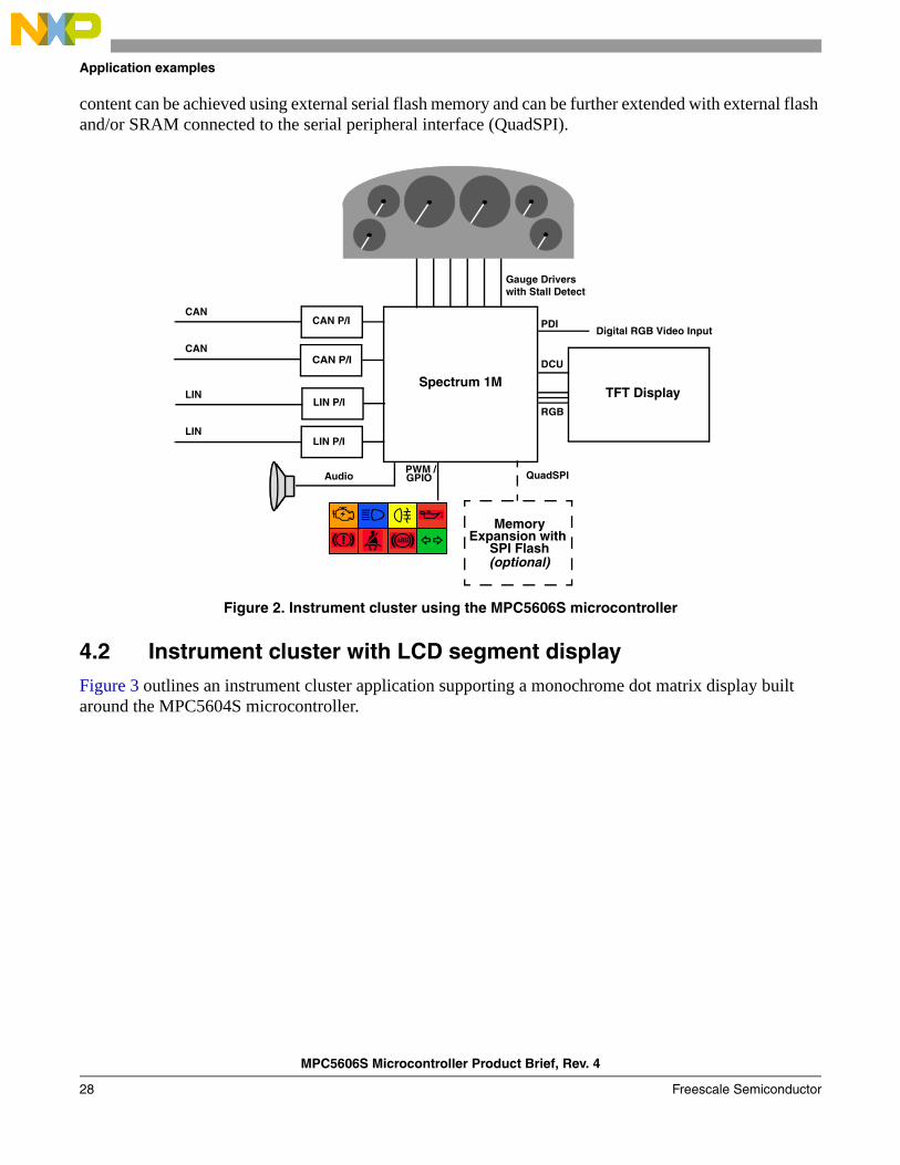
4.2 Instrument cluster with LCD segment displayFigure 3 outlines an instrument cluster application supporting a monochrome dot matrix display built around the MPC5604S microcontroller.
CAN P/I
CAN P/I
LIN P/I
LIN P/I
CAN
CAN
AudioPWM /GPIO
LIN
LIN
Gauge Driverswith Stall Detect
Spectrum 1MTFT Display
QuadSPI
DCU
PDIDigital RGB Video Input
MemoryExpansion with
SPI Flash(optional)
RGB
MPC5606S Microcontroller Product Brief, Rev. 4
Freescale Semiconductor28
Developer support
Figure 3. Instrument cluster using MPC5606S
5 Developer supportThis family of MCUs is supported by similar tools as other Freescale MPC5500 products offering a widespread, established network of tools and software vendors. It also features a high-performance Nexus debug interface.
The following development support will be available:
• Automotive Evaluation Boards (EVB) featuring CAN, LIN interfaces and more
• Compilers
• Debuggers
• JTAG and Nexus interfaces
The following software support will be available:
• OSEK solutions will be available from multiple third parties
• CAN and LIN drivers
• AUTOSAR package
CAN P/I
LIN P/I
LIN P/I
LCD Segment Display
CAN
Audio
PWM /GPIO
LIN
LIN
Gauge Driverswith Stall Detect
Spectrum 1M
Dot Matrix Display
SPI or Parallel
MPC5606S Microcontroller Product Brief, Rev. 4
Freescale Semiconductor 29
Orderable parts
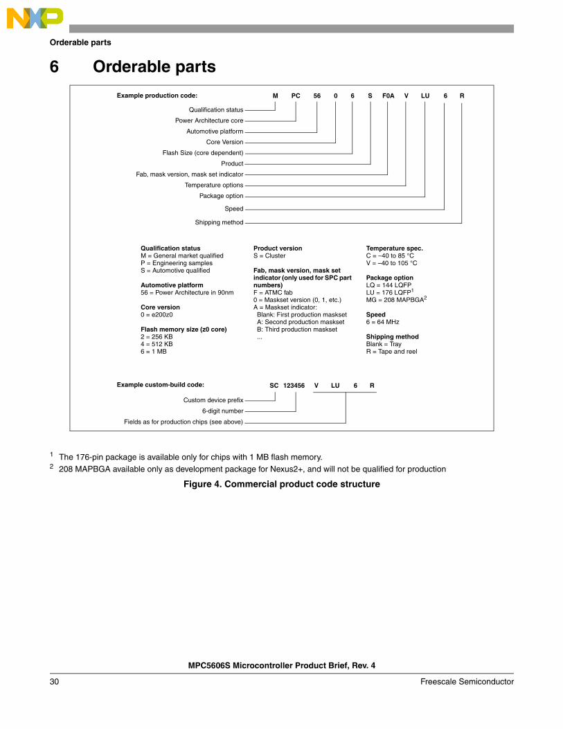
6 Orderable parts
1 The 176-pin package is available only for chips with 1 MB flash memory.2 208 MAPBGA available only as development package for Nexus2+, and will not be qualified for production
Figure 4. Commercial product code structure
Qualification status
Power Architecture core
Automotive platform
Core Version
Flash Size (core dependent)
Product
Fab, mask version, mask set indicator
M PC 56 S F0A V LUExample production code: 0 6
Temperature options
Package option
Qualification statusM = General market qualifiedP = Engineering samplesS = Automotive qualified
Automotive platform56 = Power Architecture in 90nm
Core version0 = e200z0
Flash memory size (z0 core)2 = 256 KB4 = 512 KB6 = 1 MB
Product versionS = Cluster
Fab, mask version, mask set indicator (only used for SPC part numbers)F = ATMC fab0 = Maskset version (0, 1, etc.)A = Maskset indicator:Blank: First production masksetA: Second production masksetB: Third production maskset...
Shipping method
R
Temperature spec.C = –40 to 85 °CV = –40 to 105 °C
Package optionLQ = 144 LQFPLU = 176 LQFP1
MG = 208 MAPBGA2
Speed6 = 64 MHz
Shipping methodBlank = TrayR = Tape and reel
Speed
6
Example custom-build code: SC 123456 V LU R6
Custom device prefix
6-digit number
Fields as for production chips (see above)
MPC5606S Microcontroller Product Brief, Rev. 4
Freescale Semiconductor30
Revision history
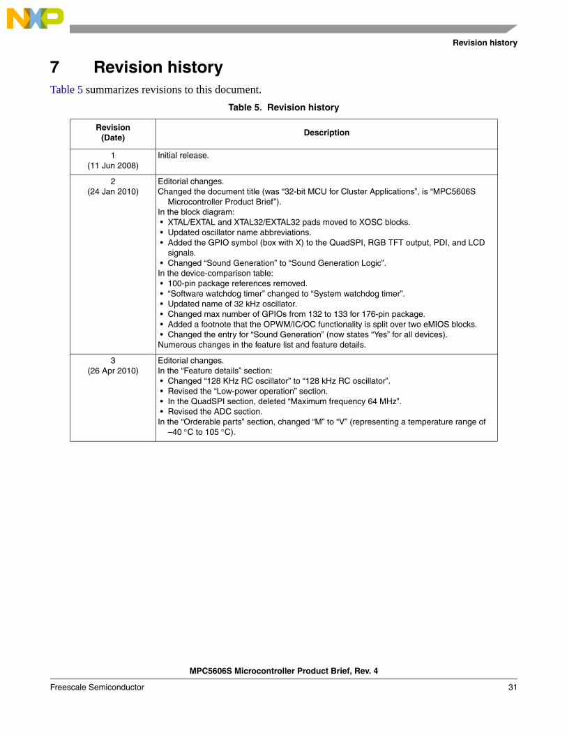
7 Revision historyTable 5 summarizes revisions to this document.
Table 5. Revision history
Revision(Date)
Description
1(11 Jun 2008)
Initial release.
2(24 Jan 2010)
Editorial changes.Changed the document title (was “32-bit MCU for Cluster Applications”, is “MPC5606S
Microcontroller Product Brief”).In the block diagram: • XTAL/EXTAL and XTAL32/EXTAL32 pads moved to XOSC blocks. • Updated oscillator name abbreviations. • Added the GPIO symbol (box with X) to the QuadSPI, RGB TFT output, PDI, and LCD
signals. • Changed “Sound Generation” to “Sound Generation Logic”.In the device-comparison table: • 100-pin package references removed. • “Software watchdog timer” changed to “System watchdog timer”. • Updated name of 32 kHz oscillator. • Changed max number of GPIOs from 132 to 133 for 176-pin package. • Added a footnote that the OPWM/IC/OC functionality is split over two eMIOS blocks. • Changed the entry for “Sound Generation” (now states “Yes” for all devices).Numerous changes in the feature list and feature details.
3(26 Apr 2010)
Editorial changes.In the “Feature details” section: • Changed “128 KHz RC oscillator” to “128 kHz RC oscillator”. • Revised the “Low-power operation” section. • In the QuadSPI section, deleted “Maximum frequency 64 MHz”. • Revised the ADC section.In the “Orderable parts” section, changed “M” to “V” (representing a temperature range of
–40 C to 105 C).
MPC5606S Microcontroller Product Brief, Rev. 4
Freescale Semiconductor 31
Revision history
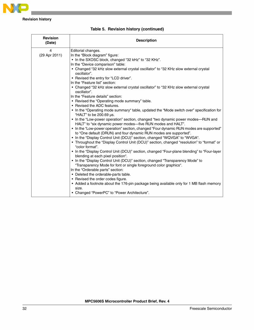
4(29 Apr 2011)
Editorial changes.In the “Block diagram” figure: • In the SXOSC block, changed “32 kHz” to “32 KHz”.In the “Device comparison” table: • Changed “32 kHz slow external crystal oscillator” to “32 KHz slow external crystal
oscillator”. • Revised the entry for “LCD driver”.In the “Feature list” section: • Changed “32 kHz slow external crystal oscillator” to “32 KHz slow external crystal
oscillator”.In the “Feature details” section: • Revised the “Operating mode summary” table. • Revised the ADC features. • In the “Operating mode summary“ table, updated the “Mode switch over” specification for
“HALT” to be 200.69 µs. • In the “Low-power operation” section, changed “two dynamic power modes—RUN and
HALT” to “six dynamic power modes—five RUN modes and HALT”. • In the “Low-power operation” section, changed “Four dynamic RUN modes are supported”
to “One default (DRUN) and four dynamic RUN modes are supported”. • In the “Display Control Unit (DCU)” section, changed “WQVGA” to “WVGA“. • Throughout the “Display Control Unit (DCU)” section, changed “resolution” to “format” or
“color format”. • In the “Display Control Unit (DCU)” section, changed “Four-plane blending” to “Four-layer
blending at each pixel position“. • In the “Display Control Unit (DCU)” section, changed “Transparency Mode” to
“Transparency Mode for font or single foreground color graphics“.In the “Orderable parts” section: • Deleted the orderable-parts table. • Revised the order codes figure. • Added a footnote about the 176-pin package being available only for 1 MB flash memory
size. • Changed “PowerPC” to “Power Architecture”.
Table 5. Revision history (continued)
Revision(Date)
Description
MPC5606S Microcontroller Product Brief, Rev. 4
Freescale Semiconductor32
How to Reach Us:
Home Page:www.freescale.com
Web Support:http://www.freescale.com/support
USA/Europe or Locations Not Listed:Freescale Semiconductor, Inc.Technical Information Center, EL5162100 East Elliot RoadTempe, Arizona 852841-800-521-6274 or +1-480-768-2130www.freescale.com/support
Europe, Middle East, and Africa:Freescale Halbleiter Deutschland GmbHTechnical Information CenterSchatzbogen 781829 Muenchen, Germany+44 1296 380 456 (English)+46 8 52200080 (English)+49 89 92103 559 (German)+33 1 69 35 48 48 (French)www.freescale.com/support
Japan:Freescale Semiconductor Japan Ltd. HeadquartersARCO Tower 15F1-8-1, Shimo-Meguro, Meguro-ku,Tokyo 153-0064Japan0120 191014 or +81 3 5437 [email protected]
Asia/Pacific:Freescale Semiconductor China Ltd.Exchange Building 23FNo. 118 Jianguo RoadChaoyang DistrictBeijing 100022China +86 10 5879 8000 [email protected]
Freescale Semiconductor Literature Distribution Center1-800-441-2447 or +1-303-675-2140Fax: +1-303-675-2150 [email protected]
Information in this document is provided solely to enable system and software implementers to use Freescale Semiconductor products. There are no express or implied copyright licenses granted hereunder to design or fabricate any integrated circuits or integrated circuits based on the information in this document.
Freescale Semiconductor reserves the right to make changes without further notice to any products herein. Freescale Semiconductor makes no warranty, representation or guarantee regarding the suitability of its products for any particular purpose, nor does Freescale Semiconductor assume any liability arising out of the application or use of any product or circuit, and specifically disclaims any and all liability, including without limitation consequential or incidental damages. “Typical” parameters that may be provided in Freescale Semiconductor data sheets and/or specifications can and do vary in different applications and actual performance may vary over time. All operating parameters, including “Typicals”, must be validated for each customer application by customer’s technical experts. Freescale Semiconductor does not convey any license under its patent rights nor the rights of others. Freescale Semiconductor products are not designed, intended, or authorized for use as components in systems intended for surgical implant into the body, or other applications intended to support or sustain life, or for any other application in which the failure of the Freescale Semiconductor product could create a situation where personal injury or death may occur. Should Buyer purchase or use Freescale Semiconductor products for any such unintended or unauthorized application, Buyer shall indemnify and hold Freescale Semiconductor and its officers, employees, subsidiaries, affiliates, and distributors harmless against all claims, costs, damages, and expenses, and reasonable attorney fees arising out of, directly or indirectly, any claim of personal injury or death associated with such unintended or unauthorized use, even if such claim alleges that Freescale Semiconductor was negligent regarding the design or manufacture of the part.
Freescale™ and the Freescale logo are trademarks of Freescale Semiconductor, Inc. The described product contains a PowerPC processor core. The PowerPC name is a trademark of IBM Corp. and used under license. All other product or service names are the property of their respective owners.
© Freescale Semiconductor, Inc. 2009–2011. All rights reserved.
MPC560xSPBRev. 404/2011