Embed Size (px)
Citation preview
Freescale SemiconductorData Sheet: Technical Data
Document Number: MPC5606SRev. 8, 11/2011
© Freescale Semiconductor, Inc., 2008–2011. All rights reserved.
MPC5606S
LQFP176 (24 x 24 mm)LQFP144 (20 x 20 mm)
MPC5606S Microcontroller Data Sheet
• Single issue, 32-bit Power Architecture Book E compliant CPU core complex (e200z0h)– Compatible with classic PowerPC instruction set– Includes variable length encoding (VLE) instruction set
for smaller code size footprint; with the encoding of mixed 16-bit and 32-bit instructions, it is possible to achieve significant code size footprint reduction over conventional Book E compliant code
• On-chip ECC flash memory with flash controller– Up to 1 MB primary flash—two 512 KB modules with
prefetch buffer and 128-bit data access port– 64 KB data flash—separate 4 16 KB flash block for
EEPROM emulation with prefetch buffer and 128-bit data access port
• Up to 48 KB on-chip ECC SRAM with SRAM controller• Up to 160 KB on-chip non-ECC graphics SRAM with
SRAM controller• Memory Protection Unit (MPU) with up to 12 region
descriptors and 32-byte region granularity to provide basic memory access permission
• Interrupt Controller (INTC) with up to 127 peripheral interrupt sources and eight software interrupts
• 2 Frequency-Modulated Phase-Locked Loops (FMPLLs)– Primary FMPLL provides a 64 MHz system clock– Auxiliary FMPLL is available for use as an alternate,
modulated or non-modulated clock source to eMIOS modules and as alternate clock to the DCU for pixel clock generation
• Crossbar switch architecture enables concurrent access of peripherals, flash memory, or RAM from multiple bus masters (AMBA 2.0 v6 AHB)
• 16-channel Enhanced Direct Memory Access controller (eDMA) with multiple transfer request sources using a DMA channel multiplexer
• Boot Assist Module (BAM) supports internal flash programming via a serial link (FlexCAN or LINFlex)
• Display Control Unit to drive TFT LCD displays
– Includes processing of up to four planes that can be blended together
– Offers a direct unbuffered hardware bit-blitter of up to 16 software-configurable dynamic layers in order to drastically minimize graphic memory requirements and provide fast animations
– Programmable display resolutions are available up to WVGA
• Parallel Data Interface (PDI) for digital video input• LCD segment driver module with two software
programmable configurations:– Up to 40 frontplane drivers and 4 backplane drivers– Up to 38 frontplane drivers and 6 backplane drivers
• Stepper Motor Controller (SMC) module with high-current drivers for up to six instrument cluster gauges driven in full dual H-Bridge configuration including full diagnostics for short circuit detection
• Stepper motor return-to-zero and stall detection module• Sound generation and playback utilizing PWM channels
and eDMA; supports monotonic and polyphonic sound• 24 eMIOS channels providing up to 16 PWM and 24 input
capture / output compare channels• 10-bit Analog-to-Digital Converter (ADC)
– Maximum conversion time of 1 s– Up to 16 internal channels, expandable to 23 via external
multiplexing• Up to 2 Deserial Serial Peripheral Interface (DSPI)
modules for full-duplex, synchronous communications with external devices (extendable to include up to 8 multiplexed external channels)
• QuadSPI serial flash memory controller supporting single, dual, and quad modes of operation to interface to external serial flash memory; QuadSPI can be configured to function as another DSPI module (MPC5606S only)
• 2 Local Interconnect Network Flexible (LINFlex) controller modules capable of autonomous message handling (master), autonomous header handling (slave
MPC5606S Microcontroller Data Sheet, Rev. 8
Freescale Semiconductor2
mode), and UART support; compliant with LIN protocol rev 2.1
• 2 full CAN 2.0B controllers with 64 configurable buffers each; bit rate programmable up to 1 Mbit/s
• Up to 4 Inter-integrated circuit (I2C) internal bus controllers with master/slave bus interface
• Up to 133 configurable general purpose pins supporting input and output operations
• Real Time Counter (RTC) with multiple clock sources:– 128 kHz slow internal RC oscillator or 16 MHz fast
internal RC oscillator supporting autonomous wakeup with 1 ms resolution with maximum timeout of 2 seconds
– 32 kHz slow external crystal oscillator, supporting wakeup with 1 s resolution and maximum timeout of one hour
– 4–16 MHz fast external crystal oscillator• System timers:
– 4-channel 32-bit System Timer Module (STM)—included in processor platform
– 4-channel 32-bit Periodic Interrupt Timer (PIT) module– Software Watchdog Timer (SWT)
• System Integration Unit (SIU) module to manage resets, external interrupts, GPIO, and pad control
• System Status and Configuration Module (SSCM) to provide information for identification of the device, last boot mode, or debug status, and provides an entry point for the censorship password mechanism
• Clock Generation Module (MC_CGM) to generate system clock sources and provide a unified register interface, enabling access to all clock sources
• Clock Monitor Unit (CMU) to monitor the integrity of the main crystal oscillator and the PLL and act as a frequency meter, measuring the frequency of one clock source and comparing it to a reference clock
• Mode Entry Module (MC_ME) to control the device power mode, in other words, Run, Halt, Stop, or Standby control mode transition sequences, and manage the power control, voltage regulator, clock generation, and clock management modules
• Reset Generation Module (MC_RGM) to manage reset assertion and release to the device at initial startup
• Nexus development interface (NDI) per IEEE-ISTO 5001-2003 Class Two Plus standard
• Device/board boundary-scan testing supported per Joint Test Action Group (JTAG) of IEEE (IEEE 1149.1)
• On-chip voltage regulator controller for regulating the 3.3 or 5 V supply voltage down to 1.2 V for core logic (requires external ballast transistor)
• The MPC5606S microcontrollers are offered in the following packages:1
– 144 LQFP, 0.5 mm pitch, 20 mm 20 mm outline– 176 LQFP, 0.5 mm pitch, 24 mm 24 mm outline– 208 MAPBGA, 1.0 mm pitch, 17 mm 17 mm outline
(not a production package; available in limited quantities for tool development only)
1. See the device comparison table or orderable parts summary for package offerings for each device in the family.
MPC5606S Microcontroller Data Sheet, Rev. 8
Freescale Semiconductor3
Table of Contents1 Overview. . . . . . . . . . . . . . . . . . . . . . . . . . . . . . . . . . . . . . . . . .4
1.1 Document overview. . . . . . . . . . . . . . . . . . . . . . . . . . . . .41.2 Description . . . . . . . . . . . . . . . . . . . . . . . . . . . . . . . . . . .41.3 Device comparison . . . . . . . . . . . . . . . . . . . . . . . . . . . . .41.4 MPC5606S series blocks . . . . . . . . . . . . . . . . . . . . . . . .51.5 Details . . . . . . . . . . . . . . . . . . . . . . . . . . . . . . . . . . . . . . .7
2 Pinout and signal descriptions . . . . . . . . . . . . . . . . . . . . . . . .232.1 144 LQFP package pinouts . . . . . . . . . . . . . . . . . . . . .232.2 176 LQFP package pinout . . . . . . . . . . . . . . . . . . . . . .272.3 208 MAPBGA package ballmap . . . . . . . . . . . . . . . . . .282.4 Pad configuration during reset phases . . . . . . . . . . . . .292.5 Voltage supply pins . . . . . . . . . . . . . . . . . . . . . . . . . . . .292.6 Pad types . . . . . . . . . . . . . . . . . . . . . . . . . . . . . . . . . . .302.7 System pins . . . . . . . . . . . . . . . . . . . . . . . . . . . . . . . . .302.8 Debug pins . . . . . . . . . . . . . . . . . . . . . . . . . . . . . . . . . .312.9 Port pin summary . . . . . . . . . . . . . . . . . . . . . . . . . . . . .33
3 Electrical characteristics . . . . . . . . . . . . . . . . . . . . . . . . . . . . .553.1 Introduction . . . . . . . . . . . . . . . . . . . . . . . . . . . . . . . . . .553.2 Parameter classification . . . . . . . . . . . . . . . . . . . . . . . .553.3 NVUSRO register . . . . . . . . . . . . . . . . . . . . . . . . . . . . .553.4 Absolute maximum ratings . . . . . . . . . . . . . . . . . . . . . .563.5 Thermal characteristics. . . . . . . . . . . . . . . . . . . . . . . . .613.6 Electromagnetic compatibility (EMC) characteristics . .633.7 Power management electrical characteristics. . . . . . . .65
3.8 I/O pad electrical characteristics . . . . . . . . . . . . . . . . . 743.9 SSD specifications. . . . . . . . . . . . . . . . . . . . . . . . . . . . 823.10 RESET electrical characteristics . . . . . . . . . . . . . . . . . 833.11 Fast external crystal oscillator (4–16 MHz) electrical
characteristics . . . . . . . . . . . . . . . . . . . . . . . . . . . . . . . 863.12 Slow external crystal oscillator (32 KHz) electrical
characteristics . . . . . . . . . . . . . . . . . . . . . . . . . . . . . . . 883.13 FMPLL electrical characteristics . . . . . . . . . . . . . . . . . 903.14 Fast internal RC oscillator (16 MHz) electrical
characteristics . . . . . . . . . . . . . . . . . . . . . . . . . . . . . . . 913.15 Slow internal RC oscillator (128 kHz) electrical
characteristics . . . . . . . . . . . . . . . . . . . . . . . . . . . . . . . 913.16 Flash memory electrical characteristics . . . . . . . . . . . 923.17 ADC electrical characteristics . . . . . . . . . . . . . . . . . . . 933.18 LCD driver electrical characteristics . . . . . . . . . . . . . 1003.19 Pad AC specifications . . . . . . . . . . . . . . . . . . . . . . . . 1003.20 AC timing . . . . . . . . . . . . . . . . . . . . . . . . . . . . . . . . . . 103
4 Package mechanical data . . . . . . . . . . . . . . . . . . . . . . . . . . 1214.1 144 LQFP . . . . . . . . . . . . . . . . . . . . . . . . . . . . . . . . . 1214.2 176 LQFP . . . . . . . . . . . . . . . . . . . . . . . . . . . . . . . . . 125
5 Ordering information . . . . . . . . . . . . . . . . . . . . . . . . . . . . . . 1286 Revision history . . . . . . . . . . . . . . . . . . . . . . . . . . . . . . . . . . 129
MPC5606S Microcontroller Data Sheet, Rev. 8
Overview
Freescale Semiconductor4
1 Overview
1.1 Document overviewThis document describes the device features and highlights important electrical and physical characteristics. For functional characteristics, see the MPC5606S Microcontroller Reference Manual.
1.2 DescriptionThe MPC5606S family of chips is designed to enable the development of automotive instrument cluster applications by providing a single-chip solution capable of hosting real-time applications and driving a TFT display directly using an on-chip color TFT display controller.
MPC5606S chips incorporate a cost-efficient host processor core compliant with the Power Architecture® embedded category. The processor is 100% user-mode compatible with the Power Architecture and capitalizes on the available development infrastructure of current Power Architecture devices with full support from available software drivers, operating systems and configuration code to assist with users' implementations.
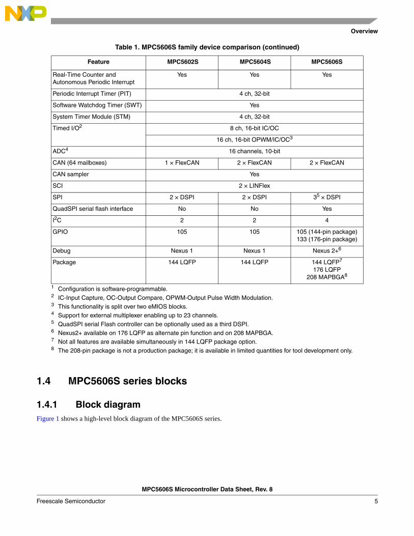
Offering high performance processing at speeds up to 64 MHz, the MPC5606S family is optimized for low power consumption and supports a range of on-chip SRAM and internal flash memory sizes. The version with 1 MB of flash memory (MPC5606S) features 160 KB of on-chip graphics SRAM.
See Table 1 for specific memory and feature sets of the product family members.
1.3 Device comparisonTable 1. MPC5606S family device comparison
Feature MPC5602S MPC5604S MPC5606S
CPU e200z0h
Execution speed Static – 64 MHz
Flash memory (ECC) 256 KB 512 KB 1 MB
EEPROM Emulation Block (ECC) 4 × 16 KB
RAM (ECC) 24 KB 48 KB 48 KB
Graphics RAM No No 160 KB
MPU 12 entry
eDMA 16 channels
Display Control Unit (DCU) No No Yes
Parallel Data Interface No No Yes
Stepper Motor Controller (SMC) 6 motors
Stepper Stall Detect (SSD) Yes
Sound Generation Logic (SGL) Yes
LCD driver 40 × 4, 38 × 61
32 KHz slow external crystal oscillator
Yes
Overview
MPC5606S Microcontroller Data Sheet, Rev. 8
Freescale Semiconductor 5
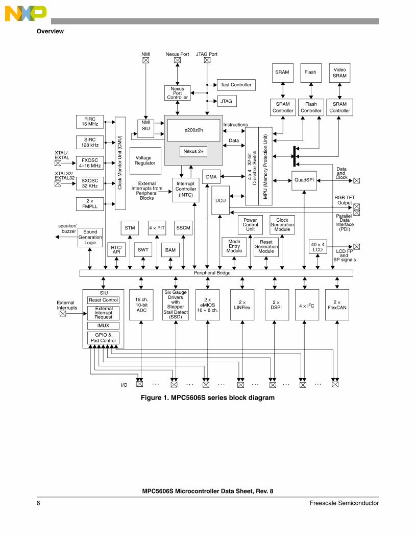
1.4 MPC5606S series blocks
1.4.1 Block diagramFigure 1 shows a high-level block diagram of the MPC5606S series.
Real-Time Counter and Autonomous Periodic Interrupt
Yes Yes Yes
Periodic Interrupt Timer (PIT) 4 ch, 32-bit
Software Watchdog Timer (SWT) Yes
System Timer Module (STM) 4 ch, 32-bit
Timed I/O2 8 ch, 16-bit IC/OC
16 ch, 16-bit OPWM/IC/OC3
ADC4 16 channels, 10-bit
CAN (64 mailboxes) 1 × FlexCAN 2 × FlexCAN 2 × FlexCAN
CAN sampler Yes
SCI 2 × LINFlex
SPI 2 × DSPI 2 × DSPI 35 × DSPI
QuadSPI serial flash interface No No Yes
I2C 2 2 4
GPIO 105 105 105 (144-pin package)133 (176-pin package)
Debug Nexus 1 Nexus 1 Nexus 2+6
Package 144 LQFP 144 LQFP 144 LQFP7
176 LQFP208 MAPBGA8
1 Configuration is software-programmable. 2 IC-Input Capture, OC-Output Compare, OPWM-Output Pulse Width Modulation. 3 This functionality is split over two eMIOS blocks. 4 Support for external multiplexer enabling up to 23 channels. 5 QuadSPI serial Flash controller can be optionally used as a third DSPI. 6 Nexus2+ available on 176 LQFP as alternate pin function and on 208 MAPBGA. 7 Not all features are available simultaneously in 144 LQFP package option. 8 The 208-pin package is not a production package; it is available in limited quantities for tool development only.
Table 1. MPC5606S family device comparison (continued)
Feature MPC5602S MPC5604S MPC5606S
MPC5606S Microcontroller Data Sheet, Rev. 8
Overview
Freescale Semiconductor6
Figure 1. MPC5606S series block diagram
Six GaugeDrivers
withStepper
Stall Detect(SSD)
16 + 8 ch.
2 ×DSPI
Test Controller
Nexus 2+
Nexus
SIU
Reset Control
Interrupt
External
IMUX
GPIO &
JTAG
Cro
ssba
r S
witc
h
Pad Control
JTAG PortNexus Port
e200z0h
External
Blocks
32-b
it
Controller
2 ×FlexCAN
4 x
4
Peripheral Bridge
PeripheralInterrupts from
InterruptRequest
ExternalInterrupts
I/O
Instructions
Data
VoltageRegulator
NMI
SWT
STM
NMISIU
. . . . . . . . .. . .
(INTC)
4 × I2C
. . .
2 ×LINFlex
2 xeMIOS
16 ch.
ADC
MP
U (
Mem
ory
Pro
tect
ion
Uni
t)
Clo
ck M
onito
r U
nit (
CM
U)
ControllerFlash
Flash
PowerControl
ModeEntry
ClockGeneration
Module
ResetGeneration
Module
Unit
ModuleBAMRTC/
SSCM
API
10-bit
. . .
DMA
DCURGB TFT
Output
Parallel Data
(PDI)Interface
SIRC
FIRC
SXOSC
FXOSC
XTAL/EXTAL
XTAL32/EXTAL32
16 MHz
128 kHz
4–16 MHz
32 KHz
4 × PIT
LCD FPand
BP signals
SoundGeneration
speaker/buzzer
Dataand ClockQuadSPI
ControllerSRAM
SRAM
2 ×FMPLL
PortController
Video
ControllerSRAM
SRAM
40 × 4LCD
Logic
Overview
MPC5606S Microcontroller Data Sheet, Rev. 8
Freescale Semiconductor 7
1.5 Details
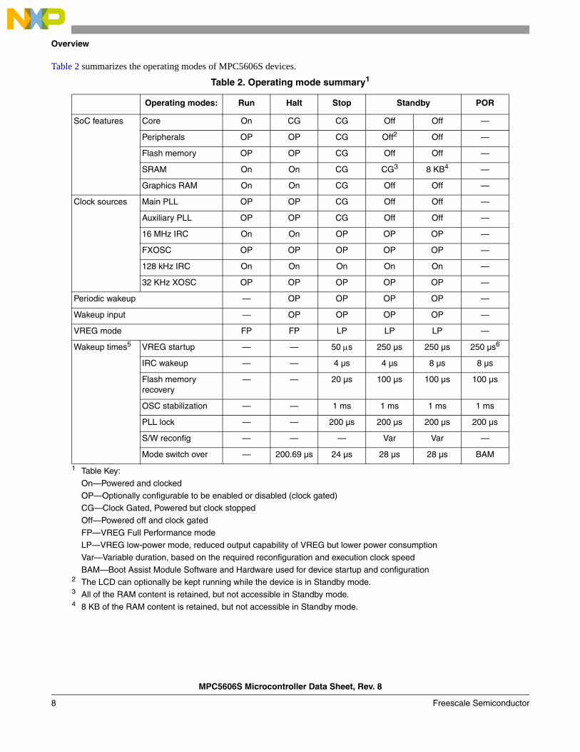
1.5.1 Low-power operationMPC5606S devices are designed for optimized low-power operation and dynamic power management of the core processor and peripherals. Power management features include software-controlled clock gating of peripherals and multiple power domains to minimize leakage in low-power modes.
There are two static low-power modes, Standby and Stop, and six dynamic power modes—five Run modes and Halt. Both low-power modes use clock gating to halt the clock for all or part of the device. Standby mode also uses power gating to automatically turn off the power supply to parts of the device to minimize leakage.
Standby mode turns off the power to the majority of the chip to offer the lowest power consumption mode. The contents of the cores, on-chip peripheral registers, and potentially some of the volatile memory are lost. Standby mode is configurable to make certain features available, with the disadvantage that these consume additional current:
• It is possible to retain the contents of the full RAM or only 8 KB.
• It is possible to enable the internal 16 MHz or 128 kHz RC oscillator, the external 4–16 MHz oscillator, or the external 32 KHz oscillator.
• It is possible to keep the LCD module active.
The device can be awakened from Standby mode from any of as many as 19 I/O pins, from a reset, or from a periodic wakeup using a low-power oscillator.
Stop mode maintains power to the entire device, thus allowing the retention of all on-chip registers and memory, and providing a faster recovery low-power mode than the lowest Standby mode. There is no need to reconfigure the device before executing code. The clocks to the core and peripherals are halted and can be optionally stopped to the oscillator or PLL at the expense of a slower startup time.
Stop mode is entered from Run mode only. Wakeup from Stop mode is triggered by an external event or by the internal periodic wakeup, if enabled.
Run modes are the primary operating modes where the entire device can be powered and clocked. In Run modes most processing activity is done. One default (Drun) and four dynamic Run modes are supported—Run0...3. The ability to configure and select different Run modes enables different clocks and power configurations to be supported with respect to each other, and to allow switching between different operating conditions. The necessary peripherals, clock sources, clock speed, and system clock prescalers can be independently configured for each of the four Run modes of the device.
Halt mode is a reduced activity, low-power mode intended for moderate periods of lower processing activity. In this mode the core system clocks are stopped but user-selected peripheral tasks can continue to run. It can be configured to provide more efficient power management features (switch-off PLL, flash memory, main regulator, etc.) at the cost of longer wakeup latency. The system returns to a Run mode as soon as an event or interrupt is pending.
MPC5606S Microcontroller Data Sheet, Rev. 8
Overview
Freescale Semiconductor8
Table 2 summarizes the operating modes of MPC5606S devices.
Table 2. Operating mode summary1
1 Table Key:
On—Powered and clocked
OP—Optionally configurable to be enabled or disabled (clock gated) CG—Clock Gated, Powered but clock stopped
Off—Powered off and clock gated
FP—VREG Full Performance mode LP—VREG low-power mode, reduced output capability of VREG but lower power consumption
Var—Variable duration, based on the required reconfiguration and execution clock speed
BAM—Boot Assist Module Software and Hardware used for device startup and configuration
Operating modes: Run Halt Stop Standby POR
SoC features Core On CG CG Off Off —
Peripherals OP OP CG Off2
2 The LCD can optionally be kept running while the device is in Standby mode.
Off —
Flash memory OP OP CG Off Off —
SRAM On On CG CG3
3 All of the RAM content is retained, but not accessible in Standby mode.
8 KB4
4 8 KB of the RAM content is retained, but not accessible in Standby mode.
—
Graphics RAM On On CG Off Off —
Clock sources Main PLL OP OP CG Off Off —
Auxiliary PLL OP OP CG Off Off —
16 MHz IRC On On OP OP OP —
FXOSC OP OP OP OP OP —
128 kHz IRC On On On On On —
32 KHz XOSC OP OP OP OP OP —
Periodic wakeup — OP OP OP OP —
Wakeup input — OP OP OP OP —
VREG mode FP FP LP LP LP —
Wakeup times5 VREG startup — — 50 s 250 µs 250 µs 250 µs6
IRC wakeup — — 4 µs 4 µs 8 µs 8 µs
Flash memory recovery
— — 20 µs 100 µs 100 µs 100 µs
OSC stabilization — — 1 ms 1 ms 1 ms 1 ms
PLL lock — — 200 µs 200 µs 200 µs 200 µs
S/W reconfig — — — Var Var —
Mode switch over — 200.69 µs 24 µs 28 µs 28 µs BAM
Overview
MPC5606S Microcontroller Data Sheet, Rev. 8
Freescale Semiconductor 9
Additional notes on low-power operation:
• Fast wakeup using the on-chip 16 MHz internal RC oscillator allows rapid execution from RAM on exit from low-power modes
• The 16 MHz internal RC oscillator supports low-speed code execution and clocking of peripherals when it is selected as the system clock and can also be used as the PLL input clock source to provide fast startup, without external oscillator delay
• MPC5606S devices include an internal voltage regulator that includes the following features:
— Regulates input to generate all internal supplies
— Manages power gating
— Low-power regulators support operation when in Stop and Standby modes to minimize power consumption
— Startup on-chip regulators in <50 s for rapid exit of Stop and Standby modes
— Low-voltage detection on main supply and 1.2 V regulated supplies
1.5.2 e200z0h core processorThe e200z0h processor is similar to other processors in the e200zx series, but supports only the VLE instruction set and does not include the signal processing extension for DSP applications or a floating point unit.
The e200z0h has all the features of the e200z0 plus:
• Branch acceleration using Branch Target Buffer (BTB)
• Supports independent instruction and data accesses to different memory subsystems, such as SRAM and flash memory via independent Instruction and Data BIUs
The e200z0h processor uses a four stage in-order pipeline for instruction execution.
1. The Instruction Fetch (stage 1)
2. Instruction Decode/Register file Read/Effective Address Calculation (stage 2)
3. Execute/Memory Access (stage 3)
4. Register Writeback (stage 4)
These stages operate in an overlapped fashion, allowing single clock instruction execution for most instructions.
The integer execution unit consists of:
• 32-bit Arithmetic Unit (AU)
• Logic Unit (LU)
• 32-bit Barrel shifter (Shifter)
• Mask-Insertion Unit (MIU)
• Condition Register manipulation Unit (CRU)
• Count-Leading-Zeros unit (CLZ)
• 8 × 32 hardware multiplier array
• Result feed-forward hardware
• Hardware divider
5 A high level summary of some key durations that need to be considered when recovering from low-power modes. This does not account for all durations at wakeup. Other delays will be necessary to consider, including but not limited to the external supply startup time. IRC wakeup time must not be added to the overall wakeup time as it starts in parallel with the VREG.All other wakeup times must be added to determine the total startup time.
6 This is the startup of the regulator that happens after the 5 V has reached beyond its POR range. If the external supply ramp rate is slow, measure from when VREG has crossed beyond the POR threshold; otherwise, this value will depend on the ramp rate of the external supply (VDDR).
MPC5606S Microcontroller Data Sheet, Rev. 8
Overview
Freescale Semiconductor10
Most arithmetic and logical operations are executed in a single cycle with the exception of the divide and multiply instructions. A Count-Leading-Zeros unit operates in a single clock cycle. The Instruction Unit contains a PC incrementer and a dedicated Branch Address adder to minimize delays during change of flow operations. Branch target prefetching from the BTB is performed to accelerate certain taken branches. Sequential prefetching is performed to ensure a supply of instructions into the execution pipeline. Prefetched instructions are placed into an instruction buffer capable of holding four instructions.
Conditional branches not taken execute in a single clock. Branches with successful target prefetching have an effective execution time of one clock on e200z0h. All other taken branches have an execution time of two clocks.
Memory load and store operations are provided for byte, halfword, and word (32-bit) data with automatic zero or sign extension of byte and halfword load data as well as optional byte reversal of data. These instructions can be pipelined to allow effective single-cycle throughput. Load and store multiple word instructions allow low overhead context save and restore operations. The load/store unit contains a dedicated effective address adder to allow effective address generation to be optimized. Also, a load-to-use dependency does not incur any pipeline bubbles for most cases.
The Condition Register unit supports the condition register (CR) and condition register operations defined by the Power Architecture. The condition register consists of eight 4-bit fields that reflect the results of certain operations, such as:
• Move
• Integer and floating-point compare
• Arithmetic
• Logical instructions
and provide a mechanism for testing and branching.
Vectored and autovectored interrupts are supported. Hardware-vectored interrupt support is provided to allow multiple interrupt sources to have unique interrupt handlers invoked with no software overhead.
The CPU includes support for Variable Length Encoding (VLE) instruction enhancements. This allows the Power Architecture instruction set to be represented by a modified instruction set made up from a mixture of 16-bit and 32-bit instructions. This results in a significantly smaller code size footprint without affecting performance noticeably.
The CPU core is enhanced by an additional interrupt source, the Non-Maskable Interrupt (NMI). This interrupt source is routed directly from package pins, via edge detection logic in the SIU to the CPU, bypassing the interrupt controller completely. Once the edge detection logic is programmed, it cannot be disabled, except by reset. The NMI is, as the name suggests, completely un-maskable and when asserted will always result in the immediate execution of the respective interrupt service routine. The NMI is not guaranteed to be recoverable.
The CPU core has an additional Wait for Interrupt instruction that is used in conjunction with low-power Stop mode. When Low-power Stop mode is selected, this instruction is executed to allow the system clock to be stopped. An external interrupt source or the system wakeup timer is used to restart the system clock and allow the CPU to service the interrupt.
Additional features include:
• Load/store unit
— 1-cycle load latency
— Misaligned access support
— No load-to-use pipeline bubbles
• Thirty-two 32-bit general purpose registers (GPRs)
• Separate instruction bus and load/store bus Harvard architecture
• Reservation instructions for implementing read-modify-write constructs
• Multi-cycle divide (divw) and load multiple (lmw) store multiple (smw) multiple class instructions; can be interrupted to prevent increases in interrupt latency
• Extensive system development support through Nexus debug port
Overview
MPC5606S Microcontroller Data Sheet, Rev. 8
Freescale Semiconductor 11
1.5.3 Crossbar switch (XBAR)The XBAR multi-port crossbar switch supports simultaneous connections between four master ports and four slave ports. The crossbar supports a 32-bit address bus width and a 32-bit data bus width.
The crossbar allows four concurrent transactions to occur from any master port to any slave port, but one of those transfers must be an instruction fetch from internal flash. If a slave port is simultaneously requested by more than one master port, arbitration logic selects the higher priority master and grants it ownership of the slave port. All other masters requesting that slave port are stalled until the higher priority master completes its transactions. Requesting masters having equal priority are granted access to a slave port in round-robin fashion, based upon the ID of the last master to be granted access.
The crossbar provides the following features:
• Four master ports:
— e200z0h core instruction port
— e200z0h core complex load/store data port
— eDMA controller
— Display control unit
• Four slave ports:
— One flash port dedicated to the CPU
— Platform SRAM
— QuadSPI serial flash controller
— One slave port combining:
– Flash port dedicated to the Display Control Unit and eDMA module
– Graphics SRAM
– Peripheral bridge
• 32-bit internal address bus, 32-bit internal data bus
1.5.4 Enhanced Direct Memory Access (eDMA)The eDMA module is a controller capable of performing complex data movements via 16 programmable channels, with minimal intervention from the host processor. The hardware micro architecture includes a DMA engine, that performs source and destination address calculations, and the actual data movement operations, along with an SRAM-based memory containing the transfer control descriptors (TCD) for the channels. This implementation is utilized to minimize the overall block size. The eDMA module provides the following features:
• 16 channels support independent 8-, 16-, or 32-bit single value or block transfers.
• Supports variable-sized queues and circular queues.
• Source and destination address registers are independently configured to post-increment or remain constant.
• Each transfer is initiated by a peripheral, CPU, periodic timer interrupt, or eDMA channel request.
• Each DMA channel can optionally send an interrupt request to the CPU on completion of a single value or block transfer.
• DMA transfers possible between system memories, QuadSPI, DSPIs, I2C, ADC, eMIOS, and General Purpose I/Os (GPIOs).
• Programmable DMA Channel Mux allows assignment of any DMA source to any available DMA channel with as many as 64 potential request sources.
1.5.5 Inter-IC communications module (I2C)The I2C module features the following:
• As many as four I2C modules supported
MPC5606S Microcontroller Data Sheet, Rev. 8
Overview
Freescale Semiconductor12
• Two-wire bi-directional serial bus for on-board communications
• Compatibility with I2C bus standard
• Multimaster operation
• Software-programmable for one of 256 different serial clock frequencies
• Software-selectable acknowledge bit
• Interrupt-driven, byte-by-byte data transfer
• Arbitration-lost interrupt with automatic mode switching from master to slave
• Calling address identification interrupt
• Start and stop signal generation/detection
• Repeated START signal generation
• Acknowledge bit generation/detection
• Bus-busy detection
1.5.6 Interrupt Controller (INTC)The INTC provides priority-based preemptive scheduling of interrupt requests, suitable for statically scheduled hard real-time systems.
For high-priority interrupt requests, the time from the assertion of the interrupt request from the peripheral to when the processor is executing the interrupt service routine (ISR) has been minimized. The INTC provides a unique vector for each interrupt request source for quick determination of which ISR needs to be executed. It also provides an ample number of priorities so that lower priority ISRs do not delay the execution of higher priority ISRs. To allow the appropriate priorities for each source of interrupt request, the priority of each interrupt request is software-configurable.
When multiple tasks share a resource, coherent accesses to that resource need to be supported. The INTC supports the priority ceiling protocol for coherent accesses. By providing a modifiable priority mask, the priority can be raised temporarily so that all tasks which share the resource cannot preempt each other.
Multiple processors can assert interrupt requests to each other through software-settable interrupt requests. These same software-settable interrupt requests also can be used to break the work involved in servicing an interrupt request into a high-priority portion and a low-priority portion. The high-priority portion is initiated by a peripheral interrupt request, but then the ISR asserts a software-settable interrupt request to finish the servicing in a lower priority ISR. Therefore these software-settable interrupt requests can be used instead of the peripheral ISR scheduling a task through the RTOS. The INTC provides the following features:
• Unique 9-bit vector for each of the possible 128 separate interrupt sources
• Eight software triggerable interrupt sources
• 16 priority levels with fixed hardware arbitration within priority levels for each interrupt source
• Ability to modify the ISR or task priority
— Modifying the priority can be used to implement the Priority Ceiling Protocol for accessing shared resources
• External NMI directly accessing the main core critical interrupt mechanism
• 32 external interrupts
1.5.7 QuadSPI serial flash controllerThe QuadSPI module enables use of external serial flash memories supporting single, dual, and quad modes of operation. It features the following:
• Memory mapping of external serial flash memory
• Automatic serial flash read command generation by CPU, DMA, or DCU read access on AHB bus
• Supports single, dual, and quad serial flash read commands
• Flexible buffering scheme to maximize read bandwidth of serial flash
Overview
MPC5606S Microcontroller Data Sheet, Rev. 8
Freescale Semiconductor 13
• Legacy mode allowing QuadSPI to be used as a standard DSPI (no DSI or CSI mode)
1.5.8 System Integration Unit (SIU)The SIU controls MCU, pad configuration, external interrupt, general purpose I/O (GPIO) and internal peripheral multiplexing.
The GPIO features the following:
• As many as four levels of internal pin multiplexing, allowing exceptional flexibility in the allocation of device functions for each package
• Centralized general purpose input output (GPIO) control of as many as 132 input/output pins (package dependent)
• All GPIO pins can be independently configured to support pullup, pulldown, or no pull
• Reading and writing to GPIO supported both as individual pins and 16-bit-wide ports
• All peripheral pins can be alternatively configured as both general purpose input or output pins, except ADC channels which support alternative configuration as general purpose inputs
• Direct readback of the pin value supported on all digital output pins through the SIU
• Configurable digital input filter that can be applied to as many as 14 general purpose input pins for noise elimination on external interrupts
• Register configuration protected against change with soft lock for temporary guard or hard lock to prevent modification until next reset
1.5.9 Flash memoryThe MPC5606S microcontroller has the following flash memory features:
• As nuch as 1 MB of burst flash memory
— Typical flash memory access time: 0 wait state for buffer hits, 2 wait states for page buffer miss at 64 MHz
— Two 4128-bit page buffers with programmable prefetch control
– One set of page buffers can be allocated for code-only, fixed partitions of code and data, all available for any access
– One set of page buffers allocated to Display Controller Unit and the eDMA
— 64-bit ECC with single-bit correction, double-bit detection for data integrity
— 64 KB data flash memory — separate 416 KB flash block for EEPROM emulation with prefetch buffer and 128-bit data access port
• Small block flash memory arrangement to support features such as boot block, operating system block
• Hardware-managed flash memory writes, erases and verify sequences
• Censorship protection scheme to prevent flash memory content visibility
• Separate dedicated 64 KB data flash memory for EEPROM emulation
— Four erase sectors each containing 16 KB of memory
— Offers Read-While-Write functionality from main program space
— Same data retention and program erase specification as main program flash memory array
1.5.10 SRAMThe MPC5606S microcontrollers have as much as 48 KB general-purpose on-chip SRAM with the following features:
• Typical SRAM access time: 0 wait-state for reads and 32-bit writes; 1 wait state for 8- and 16-bit writes if back to back with a read to same memory block
• 32-bit ECC with single-bit correction, double bit detection for data integrity
• Supports byte (8-bit), half word (16-bit), and word (32-bit) writes for optimal use of memory
• User transparent ECC encoding and decoding for byte, half word, and word accesses
MPC5606S Microcontroller Data Sheet, Rev. 8
Overview
Freescale Semiconductor14
• Separate internal power domain applied to full SRAM block, 8 KB SRAM block during Standby modes to retain contents during low-power mode.
1.5.11 On-chip graphics SRAMThe MPC5606S microcontroller has 160 KB on-chip graphics SRAM with the following features:
• Usable as general purpose SRAM
• Typical SRAM access time: 0 wait-state for reads and 32-bit writes
• Supports byte (8-bit), half word (16-bit), and word (32-bit) writes for optimal use of memory
1.5.12 Memory Protection Unit (MPU)The MPU features the following:
• 12 region descriptors for per-master protection
• Start and end address defined with 32-byte granularity
• Overlapping regions supported
• Protection attributes can optionally include process ID
• Protection offered for three concurrent read ports
• Read and write attributes for all masters
• Execute and supervisor/user mode attributes for processor masters
1.5.13 Boot Assist Module (BAM)The BAM is a block of read-only memory that is programmed once by Freescale. The BAM program is executed every time the MCU is started up or reset in normal mode. The BAM supports different modes of booting. They are:
• Booting from internal flash memory
• Serial boot loading (a program is downloaded into RAM via FlexCAN or LINFlex and then executed)
• Booting from external memory
Additionally the BAM:
• Enables and manages the transition of the MCU from reset to user code execution
• Configures device for serial bootload
• Enables multiple bootcode starting locations out of reset through implementation of search for valid Reset Configuration Halfword
1.5.14 Enhanced Modular Input/Output System (eMIOS)MPC5606S microcontrollers have two eMIOS modules—one with 16 channels and one with eight—with input/output channels supporting a range of 16-bit input capture, output compare, and Pulse Width Modulation functions.
The modules are configurable and can implement 8-channel, 16-bit input capture/output compare or 16-channel, 16-bit output pulse width modulation/input compare/output compare. As many as five additional channels are configurable as modulus counters.
eMIOS other features include:
• Selectable clock source from main FMPLL, auxiliary FMPLL, external 4–16 MHz oscillator or 16 MHz internal RC oscillator
• Timed I/O channels with 16-bit counter resolution
• Buffered updates
• Support for shifted PWM outputs to minimize occurrence of concurrent edges
Overview
MPC5606S Microcontroller Data Sheet, Rev. 8
Freescale Semiconductor 15
• Edge-aligned output pulse width modulation
— Programmable pulse period and duty cycle
— Supports 0% and 100% duty cycle
— Shared or independent time bases
• Programmable phase shift between channels
• Selectable combination of pairs of eMIOS outputs to support sound generation
• DMA transfer support
• Selectable clock source from the primary FMPLL, auxiliary FMPLL, external 4–16 MHz oscillator, or the 16 MHz internal RC oscillator.
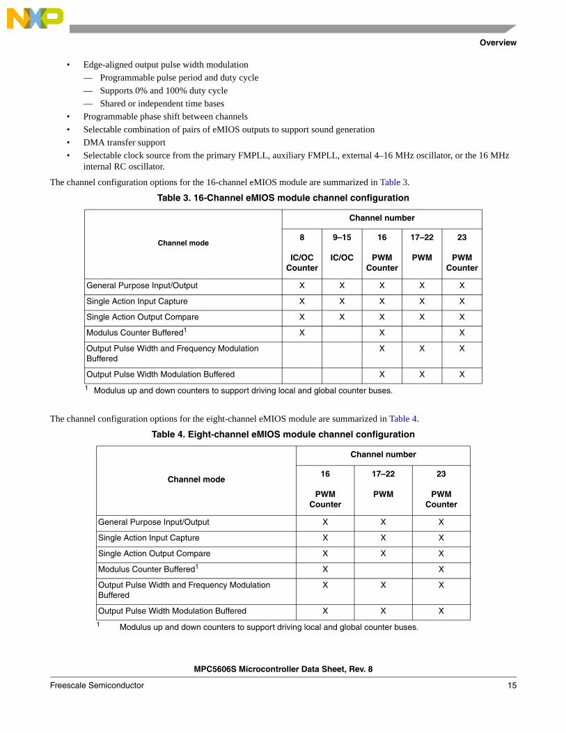
The channel configuration options for the 16-channel eMIOS module are summarized in Table 3.
The channel configuration options for the eight-channel eMIOS module are summarized in Table 4.
Table 3. 16-Channel eMIOS module channel configuration
Channel mode
Channel number
8
IC/OCCounter
9–15
IC/OC
16
PWMCounter
17–22
PWM
23
PWMCounter
General Purpose Input/Output X X X X X
Single Action Input Capture X X X X X
Single Action Output Compare X X X X X
Modulus Counter Buffered1
1 Modulus up and down counters to support driving local and global counter buses.
X X X
Output Pulse Width and Frequency Modulation Buffered
X X X
Output Pulse Width Modulation Buffered X X X
Table 4. Eight-channel eMIOS module channel configuration
Channel mode
Channel number
16
PWMCounter
17–22
PWM
23
PWMCounter
General Purpose Input/Output X X X
Single Action Input Capture X X X
Single Action Output Compare X X X
Modulus Counter Buffered1
1 Modulus up and down counters to support driving local and global counter buses.
X X
Output Pulse Width and Frequency Modulation Buffered
X X X
Output Pulse Width Modulation Buffered X X X
MPC5606S Microcontroller Data Sheet, Rev. 8
Overview
Freescale Semiconductor16
1.5.15 Analog-to-Digital Converter (ADC)The ADC features the following:
• 10-bit A/D resolution
• 0 to 5 V common mode conversion range
• Supports conversions speeds of up to 1 µs
• 16 internal and eight external channel support
• As many as 16 single-ended input channels
— All channels configured to have alternate function as general purpose input/output pins
– 10-bit ±3 counts accuracy (TUE)
• External multiplexer support to increase as many as 23 channels
— Automatic 1 × 8 multiplexer control
— External multiplexer connected to a dedicated input channel
— Shared register between the eight external channels
• Result register available for every non-multiplexed channel
• Configurable left- or right-aligned result format
• Supports for one-shot, scan, and injection conversion modes
• Injection mode status bit implemented on adjacent 16-bit register for each result
— Supports access to result and injection status with single 32-bit read
• Independent enabling of function for channels:
— Offset refresh
• Conversion Triggering support
— Internal conversion triggering from periodic interrupt timer (PIT)
• Four configurable analog comparator channels offering range comparison with triggered alarm
— Greater than
— Less than
— Out of range
• All unused analog inputs can be used as general purpose input and output pins
• Power Down mode
• Optional support for DMA transfer of results
1.5.16 Deserial Serial Peripheral Interface (DSPI)The deserial serial peripheral interface (DSPI) modules provide a synchronous serial interface for communication between the MPC5606S MCU and external devices.
The DSPI features the following:
• As many as two DSPI modules
• Full-duplex, synchronous transfers
• Master or slave operation
• Programmable master bit rates
• Programmable clock polarity and phase
• End-of-transmission interrupt flag
• Programmable transfer baud rate
• Programmable data frames from 4 to 16 bits
• As many as six chip select lines available, depending on package and pin multiplexing, enable 64 external devices to be selected using external muxing from a single DSPI
Overview
MPC5606S Microcontroller Data Sheet, Rev. 8
Freescale Semiconductor 17
• Eight clock and transfer attributes registers
• Chip select strobe available as alternate function on one of the chip select pins for deglitching
• FIFOs for buffering as many as four transfers on the transmit and receive side
• General purpose I/O functionality on pins when not used for SPI
• Queueing operation possible through use of eDMA
1.5.17 FlexCANThe MPC5606S MCU contains two controller area network (FlexCAN) modules. The FlexCAN module is a communication controller implementing the CAN protocol according to Bosch Specification version 2.0B. The CAN protocol was designed to be used primarily as a vehicle serial data bus, meeting the specific requirements of this field: real-time processing, reliable operation in the EMI environment of a vehicle, cost-effectiveness, and required bandwidth.
The FlexCan modules offer the following:
• Compliant with CAN protocol specification, Version 2.0B active
• 64 mailboxes, each configurable as transmit or receive
— Mailboxes configurable while module remains synchronized to CAN bus
• Transmit features
— Supports configuration of multiple mailboxes to form message queues of scalable depth
— Arbitration scheme according to message ID or message buffer number
— Internal arbitration to guarantee no inner or outer priority inversion
— Transmit abort procedure and notification
• Receive features
— Individual programmable filters for each mailbox
— Eight mailboxes configurable as a 6-entry receive FIFO
— Eight programmable acceptance filters for receive FIFO
• Programmable clock source
— System clock
— Direct oscillator clock to avoid PLL jitter
• Listen-only mode capabilities
• CAN Sampler
— Can catch the first message sent on the CAN network while the MPC5606S is stopped; this guarantees a clean startup of the system without missing messages on the CAN network
— CAN sampler is connected to one of the CAN RX pins
1.5.18 Serial communication interface module (LINFlex) The MPC5606S devices include as many as two LINFlex modules and support for LIN Master mode, LIN Slave mode, and UART mode. The modules are LIN state machine-compliant to the LIN 1.3 and 2.0 and 2.1 specifications and handle LIN frame transmission and reception without CPU intervention.
Other features include:
• Autonomous LIN frame handling
• Message buffer to store identifier and as many as 8 data bytes
• Supports message length as long as 64 bytes
• Detection and flagging of LIN errors
• Sync field, Delimiter, ID parity, Bit, Framing, Checksum, and Timeout errors
• Classic or extended checksum calculation
MPC5606S Microcontroller Data Sheet, Rev. 8
Overview
Freescale Semiconductor18
• Configurable break duration as long as 36-bit times
• Programmable baud rate prescalers (13-bit mantissa, 4-bit fractional)
• Diagnostic features
— Loopback
— Self-test
— LIN bus stuck dominant detection
• Interrupt-driven operation with 16 interrupt sources
• LIN slave mode features
— Autonomous LIN header handling
— Autonomous LIN response handling
— Discarding of irrelevant LIN responses using as many as 16 ID filters
• UART mode
— Full-duplex operation
— Standard non-return-to-zero (NRZ) mark/space format
— Data buffers with 4-byte receive, 4-byte transmit
— Configurable word length (8-bit or 9-bit words)
— Error detection and flagging
– Parity, noise, and framing errors
— Interrupt driven operation with four interrupt sources
— Separate transmitter and receiver CPU interrupt sources
— 16-bit programmable baud-rate modulus counter and 16-bit fractional
— Two receiver wakeup methods
1.5.19 System clocks and clock generation modulesThe system clock on the MPC5606S can be derived from an external oscillator, an on-chip FMPLL, or the internal 16 MHz oscillator.
• Source system clock frequency can be changed via an on-chip programmable clock divider (1 to 2)
• Additional programmable peripheral bus clock divider ratio (1 to 16)
• Two on-chip FMPLLs—the primary module and an auxiliary module
— Each FMPLL features:
– Input clock frequency from 4 MHz to 16 MHz
– Lock detect circuitry continuously monitoring lock status
– Loss Of Clock (LOC) detection for reference and feedback clocks
– On-chip loop filter (for improved electromagnetic interference performance and reduction of number of external components required)
– Support for frequency ramping from PLL
— The primary FMPLL module is for use as a system clock source; the auxiliary FMPLL is available for use as an alternate, modulated or non-modulated clock source to eMIOS modules and as alternate clock to the DCU for pixel clock generation
• The main oscillator provides the following features:
— Input frequency range 4–16 MHz
— Square-wave input mode
— Oscillator input mode 3.3 V (5.0 V)
— Automatic level control
— PLL reference
Overview
MPC5606S Microcontroller Data Sheet, Rev. 8
Freescale Semiconductor 19
• MPC5606S includes a 32 KHz low-power external oscillator for slow execution, reduced power consumption, and Real Time Clock
• Dedicated internal 128 kHz RC oscillator for low-power mode operation and self wakeup
— ±10% accuracy across voltage and temperature (after factory trimming)
— Trimming registers to support improved accuracy with in-application calibration
• Dedicated 16 MHz internal RC oscillator
— Used as default clock source out of reset
— Provides a clock for rapid startup from low-power modes
— Provides a backup clock in the event of PLL or external oscillator clock failure
— Offers an independent clock source for the watchdog timer
— ±5% accuracy across voltage and temperature (after factory trimming)
— Trimming registers to support frequency adjustment with in-application calibration
1.5.20 Periodic Interrupt Timer module (PIT)The PIT features the following:
• Four general-purpose interrupt timers
• As many as two dedicated interrupt timers for triggering ADC conversions
• 32-bit counter resolution
• Clocked by system clock frequency
• 32-bit counter for Real Time Interrupt, clocked from main external oscillator
1.5.21 Real Time Counter (RTC)The RTC supports wakeup from low-power modes or Real Time Clock generation
• Configurable resolution for different timeout periods
— 1 s resolution for >1 hour period
— 1 ms resolution for 2 second period
• Selectable clock sources from external 32 KHz crystal, external 4–16 MHz crystal, internal 128 kHz RC oscillator, or divided internal 16 MHz RC oscillator
1.5.22 System Timer Module (STM)The STM is a 32-bit timer designed to support commonly required system and application software timing functions. The STM includes a 32-bit up counter and four 32-bit compare channels with a separate interrupt source for each channel. The counter is driven by the system clock divided by an 8-bit prescale value (1 to 256).
• One 32-bit up counter with 8-bit prescaler
• Four 32-bit compare channels
• Independent interrupt source for each channel
• Counter can be stopped in debug mode
1.5.23 Software Watchdog Timer (SWT)The Watchdog features the following:
• Watchdog can be activated by software or enabled out of reset
• Supports normal or windowed mode
• Watchdog timer value writable once after reset
MPC5606S Microcontroller Data Sheet, Rev. 8
Overview
Freescale Semiconductor20
• Configurable response on timeout: reset, interrupt, or interrupt followed by reset
• Selectable clock source for main system clock or internal 16 MHz RC oscillator clock
1.5.24 Display Control Unit (DCU)The DCU is a display controller designed to drive TFT LCD displays capable of driving screens with resolution as high as Wide Quarter Video Graphics Array (WQVGA), with 16 layers and four planes with real time alpha-blending.
The DCU generates all the necessary signals required to drive the display: up to 24-bit RGB data bus, Pixel Clock, Data Enable, Horizontal-Sync and Vertical-Sync.
The internal memory resources of the MPC5606S allow easy management of complex graphics contents (pictures, icons, languages, fonts) on a color TFT panel in up to WQVGA sizes. All the data fetches from internal and/or external memory are performed by the internal four-channel DMA of the DCU providing a high speed/low latency access to the system backbone.
Control Descriptors (CDs) associated with each layer enable effective merging of different color formats into one plane to optimize use of internal memory buffers. A layer may be constructed from graphic content of various color formats including 1bpp, 2bpp, 4bpp, 8bpp, 16bpp, 24bpp, and 24bpp+alpha. The ability of the DCU to handle input data in formats as low as 1bpp, 2bpp, and 4bpp enables highly efficient use of internal memory resources of the MPC5606S. A special tiled mode can be enabled on any of the 16 layers to repeat a pattern, optimizing graphic memory usage.
A hardware cursor can be managed independently of the layers at blending level, increasing the efficient use of internal DCU resources.
To secure the content of all critical information to be displayed, a safety mode can be activated to check the integrity of critical data along the whole system data path from the memory to the TFT pads.
The DCU features the following:
• Display color depth: up to 24 bpp
• Generation of all RGB and control signals for TFT
• Four-layer blending at each pixel position
• Maximum number of input layers: 16 (fixed priority)
• Dynamic Look-Up Table (color and gamma look-up)
• blending range: up to 256 levels
• Transparency mode for font or single foreground color graphics
• Gamma correction
• Tiled mode on all the layers
• Hardware cursor
• Critical display content integrity monitoring for Functional Safety support
• Internal Direct Memory Access (DMA) module to transfer data from internal and/or external memory
1.5.25 Parallel Data Interface (PDI)The PDI is a digital interface used to receive external digital video or graphic content into the DCU.
The PDI input is directly injected into the DCU background plane FIFO. When the PDI is activated, all the DCU synchronization is extracted from the external video stream to guarantee the synchronization of the two video sources.
The PDI can be used to:
• Connect a video camera output directly to the PDI
• Connect a secondary display driver as slave with a minimum of extra cost
• Connect a device gathering various video sources
• Provide flexibility to allow the DCU to be used in slave mode (external synchronization)
Overview
MPC5606S Microcontroller Data Sheet, Rev. 8
Freescale Semiconductor 21
The PDI features the following:
• Supported color modes:
— 8-bit mono
— 8-bit color multiplexed
— RGB565
— 16-bit/18-bit RAW color
• Supported synchronization modes:
— Embedded ITU-R BT.656-4 (RGB565 mode 2)
— HSYNC, VSYNC
— Data enable
• Direct interface with DCU background plane FIFO
• Synchronization generation for the DCU
1.5.26 Liquid Crystal Display (LCD) driverThe LCD driver module has two configurations allowing a maximum of 160 or 228 LCD segments:
• As many as 40 frontplane drivers and four backplane drivers
• As many as 38 frontplane drivers and six backplane drivers
Each segment is controlled and can be masked by a corresponding bit in the LCD RAM.
Four to six multiplex modes (1/1, 1/2, 1/3, 1/4, 1/5, 1/6 duty), and three bias (1/1, 1/2, 1/3) methods are available. All frontplane and backplane pins can be multiplexed with other port functions.
The LCD driver module features the following:
• Programmable frame clock generator from different clock sources:
— System clock
— Internal RC oscillator
• Programmable bias voltage level selector
• On-chip generation of all output voltage levels
— LCD voltage reference taken from main 5 V supply
• LCD RAM – contains the data to be displayed on the LCD
— Data can be read from or written to the display RAM at any time
• End-of-frame interrupt:
— Optimize data refresh without visual artifacts
— Selectable number of frames between each interrupt
• Contrast adjustment using programmable internal voltage reference
• Remapping capability of four or six backplanes with frontplanes
— Increases pin selection flexibility
• In low-power modes, LCD operation can be suspended under software control; the LCD can also operate in low-power modes, clocked by the internal 128 kHz IRC or external 32 KHz crystal oscillator
• Selectable output current boost during transitions
1.5.27 Stepper Motor Controller (SMC)The SMC module is a PWM motor controller suitable to drive instruments in a cluster configuration or any other loads requiring a PWM signal. The motor controller has twelve PWM channels associated with two pins each (24 pins in total).
The SMC module includes the following features:
MPC5606S Microcontroller Data Sheet, Rev. 8
Overview
Freescale Semiconductor22
• 10/11-bit PWM counter
• 11-bit resolution with selectable PWM dithering function
• Left-, right-, or center-aligned PWM
• Output slew rate control
• Output short-circuit detection
This module is suited for, but not limited to, driving small stepper and air core motors used in instrumentation applications. This module can be used for other motor control or PWM applications that match the frequency, resolution, and output drive capabilities of the module.
1.5.28 Stepper Stall Detect (SSD)The stepper stall detector (SSD) module provides a circuit to measure and integrate the induced voltage on the non-driven coil of a stepper motor using full steps when the gauge pointer is returning to zero (RTZ).
The SSD module features the following:
• Programmable full step state
• Programmable integration polarity
• Blanking (recirculation) state
• 16-bit integration accumulator register
• 16-bit modulus down counter with interrupt
1.5.29 Sound Generation Logic (SGL)The SGL has two modes of operation:
• Amplitude-modulated PWM mode for low-cost buzzers using any two eMIOS channels:
— Monophonic signal with amplitude control
— 8-bit amplitude resolution
— Ability to mix any two eMIOS channels
— Requires simple external RC lowpass filter
• Digital sample mode for higher quality sound using one eMIOS channel and eDMA
— Up to 10-bit audio amplitude resolution
— Polyphonic sound synthesis
— Playback of sample-based waveforms
— Text-to-speech possibility
— Requires external lowpass filter
1.5.30 IEEE 1149.1 JTAG Controller (JTAGC)JTAGC features the following:
• Backward compatible to standard JTAG IEEE 1149.1-2001 test access port (TAP) interface
• Support for boundary scan testing
1.5.31 Nexus Development Interface (NDI)Nexus features the following:
• Per IEEE-ISTO 5001-2003
• Nexus 2 Plus features supported
Pinout and signal descriptions
MPC5606S Microcontroller Data Sheet, Rev. 8
Freescale Semiconductor 23
— Static debug
— Watchpoint messaging
— Ownership trace messaging
— Program trace messaging
— Real time read/write of any internally memory-mapped resources through JTAG pins
— Overrun control, which selects whether to stall before Nexus overruns or else keep executing and allow overwrite of information
— Watchpoint triggering, watchpoint triggers program tracing
• Configured via the IEEE 1149.1 (JTAG) port
• Nexus Auxiliary port supported on the 176 LQFP and 208-pin BGA package FOR DEVELOPMENT ONLY
— Narrow Auxiliary Nexus port supporting support trace, with two MDO pins
— Wide Auxiliary Nexus port supporting higher bandwidth trace, with four MDO pins
2 Pinout and signal descriptions
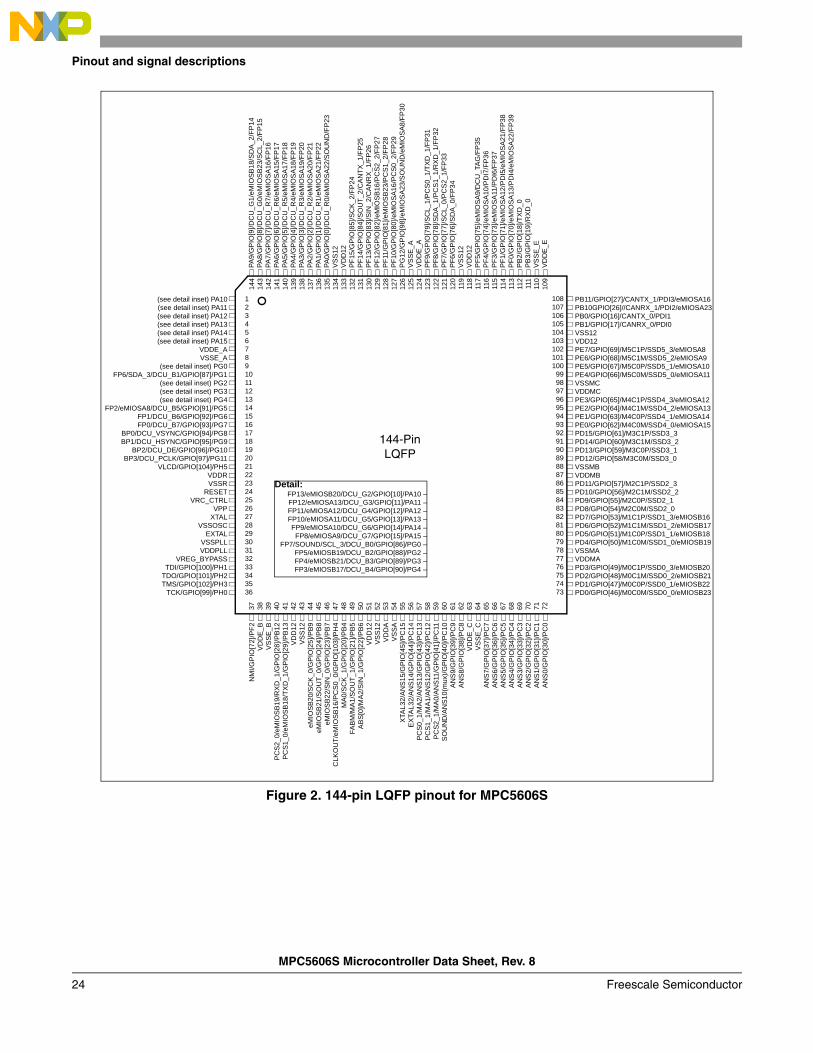
2.1 144 LQFP package pinoutsThis section shows the pinouts for the 144-pin LQFP packages.
CAUTIONAny pins labeled “NC” must not be connected to any external circuit.
MPC5606S Microcontroller Data Sheet, Rev. 8
Pinout and signal descriptions
Freescale Semiconductor24
Figure 2. 144-pin LQFP pinout for MPC5606S
37 38 39 40 41 42 43 44 45 46 47 48 49 50 51 52 53 54 55 56 57 58 59 60 61 62 63 64 65 66 67 68 69 70 71 72
123456789101112131415161718192021222324252627282930313233343536
108107106105104103102101100
999897969594939291908988878685848382818079787776757473
144-PinLQFP
144
143
142
141
140
139
138
137
136
135
134
133
132
131
130
129
128
127
126
125
124
123
122
121
120
119
118
117
116
115
114
113
112
111
110
109
NM
I/GP
IO[7
2]/P
F2
VD
DE
_B
VS
SE
_B
PC
S2_
0/eM
IOS
B19
/RX
D_1
/GP
IO[2
8]/P
B12
PC
S1_
0/eM
IOS
B18
/TX
D_1
/GP
IO[2
9]/P
B13
VD
D1
2V
SS
12
eMIO
SB
20/S
CK
_0/
GP
IO[2
5]/P
B9
eM
IOS
B2
1/S
OU
T_
0/G
PIO
[24
]/P
B8
eMIO
SB
22/S
IN_
0/G
PIO
[23]
/PB
7C
LKO
UT
/eM
IOS
B16
/PC
S0
_0/G
PIO
[103
]/PH
4M
A0/
SC
K_
1/G
PIO
[20]
/PB
4F
AB
M/M
A1/
SO
UT
_1/
GP
IO[2
1]/P
B5
AB
S[0
]/MA
2/S
IN_
1/G
PIO
[22
]/P
B6
VD
D1
2V
SS
12
VD
DA
VS
SA
XTA
L32
/AN
S15
/GP
IO[4
5]/P
C15
EX
TAL
32/A
NS
14/
GP
IO[4
4]/P
C14
PC
S0_
1/M
A2
/AN
S13
/GP
IO[4
3]/P
C13
PC
S1_
1/M
A1
/AN
S12
/GP
IO[4
2]/P
C12
PC
S2_
1/M
A0/
AN
S11
/GP
IO[4
1]/P
C11
SO
UN
D/A
NS
10
(mux
)/G
PIO
[40]
/PC
10
AN
S9
/GP
IO[3
9]/P
C9
AN
S8
/GP
IO[3
8]/P
C8
VD
DE
_C
VS
SE
_C
AN
S7
/GP
IO[3
7]/P
C7
AN
S6
/GP
IO[3
6]/P
C6
AN
S5
/GP
IO[3
5]/P
C5
AN
S4
/GP
IO[3
4]/P
C4
AN
S3
/GP
IO[3
3]/P
C3
AN
S2
/GP
IO[3
2]/P
C2
AN
S1
/GP
IO[3
1]/P
C1
AN
S0
/GP
IO[3
0]/P
C0
PA
9/G
PIO
[9]/D
CU
_G1/
eMIO
SB
18/S
DA
_2/F
P14
PA
8/G
PIO
[8]/D
CU
_G0/
eMIO
SB
23/S
CL_
2/F
P15
PA
7/G
PIO
[7]/D
CU
_R7/
eMIO
SA
16/F
P16
PA
6/G
PIO
[6]/D
CU
_R6/
eMIO
SA
15/F
P17
PA
5/G
PIO
[5]/D
CU
_R5/
eMIO
SA
17/F
P18
PA
4/G
PIO
[4]/D
CU
_R4/
eMIO
SA
18/F
P19
PA
3/G
PIO
[3]/D
CU
_R3/
eMIO
SA
19/F
P20
PA
2/G
PIO
[2]/D
CU
_R2/
eMIO
SA
20/F
P21
PA
1/G
PIO
[1]/D
CU
_R1/
eMIO
SA
21/F
P22
PA
0/G
PIO
[0]/D
CU
_R
0/e
MIO
SA
22
/SO
UN
D/F
P2
3V
SS
12
VD
D12
PF
15/G
PIO
[85]
/SC
K_2
/FP
24P
F14
/GP
IO[8
4]/S
OU
T_2
/CA
NT
X_1
/FP
25P
F13
/GP
IO[8
3]/S
IN_2
/CA
NR
X_1
/FP
26P
F12
/GP
IO[8
2]/e
MIO
SB
16/P
CS
2_2
/FP
27P
F11
/GP
IO[8
1]/e
MIO
SB
23/P
CS
1_2/
FP
28
PF
10/G
PIO
[80]
/eM
IOS
A16
/PC
S0
_2/F
P29
PG
12/
GP
IO[9
8]/e
MIO
SA
23
/SO
UN
D/e
MIO
SA
8/F
P3
0V
SS
E_
AV
DD
E_
AP
F9/
GP
IO[7
9]/S
CL_
1/P
CS
0_1/
TX
D_1
/FP
31P
F8/
GP
IO[7
8]/S
DA
_1/P
CS
1_1
/RX
D_1
/FP
32P
F7/
GP
IO[7
7]/S
CL_
0/P
CS
2_1/
FP
33P
F6/
GP
IO[7
6]/S
DA
_0/F
P34
VS
S1
2V
DD
12P
F5/
GP
IO[7
5]/e
MIO
SA
9/D
CU
_TA
G/F
P35
PF
4/G
PIO
[74]
/eM
IOS
A10
/PD
I7/F
P3
6P
F3/
GP
IO[7
3]/e
MIO
SA
11/P
DI6
/FP
37P
F1/
GP
IO[7
1]/e
MIO
SA
12/P
DI5
/eM
IOS
A21
/FP
38P
F0/
GP
IO[7
0]/e
MIO
SA
13/P
DI4
/eM
IOS
A22
/FP
39P
B2
/GP
IO[1
8]/T
XD
_0
PB
3/G
PIO
[19
]/RX
D_
0V
SS
E_
EV
DD
E_
E
PB11/GPIO[27]/CANTX_1/PDI3/eMIOSA16PB10GPIO[26]//CANRX_1/PDI2/eMIOSA23PB0/GPIO[16]/CANTX_0/PDI1PB1/GPIO[17]/CANRX_0/PDI0VSS12VDD12PE7/GPIO[69]/M5C1P/SSD5_3/eMIOSA8PE6/GPIO[68]/M5C1M/SSD5_2/eMIOSA9PE5/GPIO[67]/M5C0P/SSD5_1/eMIOSA10PE4/GPIO[66]/M5C0M/SSD5_0/eMIOSA11VSSMCVDDMCPE3/GPIO[65]/M4C1P/SSD4_3/eMIOSA12PE2/GPIO[64]/M4C1M/SSD4_2/eMIOSA13PE1/GPIO[63]/M4C0P/SSD4_1/eMIOSA14PE0/GPIO[62]/M4C0M/SSD4_0/eMIOSA15PD15/GPIO[61]/M3C1P/SSD3_3PD14/GPIO[60]/M3C1M/SSD3_2PD13/GPIO[59]/M3C0P/SSD3_1PD12/GPIO[58/M3C0M/SSD3_0VSSMBVDDMBPD11/GPIO[57]/M2C1P/SSD2_3PD10/GPIO[56]/M2C1M/SSD2_2PD9/GPIO[55]/M2C0P/SSD2_1PD8/GPIO[54]/M2C0M/SSD2_0PD7/GPIO[53]/M1C1P/SSD1_3/eMIOSB16PD6/GPIO[52]/M1C1M/SSD1_2/eMIOSB17PD5/GPIO[51]/M1C0P/SSD1_1/eMIOSB18PD4/GPIO[50]/M1C0M/SSD1_0/eMIOSB19VSSMAVDDMAPD3/GPIO[49]/M0C1P/SSD0_3/eMIOSB20PD2/GPIO[48]/M0C1M/SSD0_2/eMIOSB21PD1/GPIO[47]/M0C0P/SSD0_1/eMIOSB22PD0/GPIO[46]/M0C0M/SSD0_0/eMIOSB23
(see detail inset) PA10(see detail inset) PA11(see detail inset) PA12(see detail inset) PA13(see detail inset) PA14(see detail inset) PA15
VDDE_AVSSE_A
(see detail inset) PG0FP6/SDA_3/DCU_B1/GPIO[87]/PG1
(see detail inset) PG2(see detail inset) PG3(see detail inset) PG4
FP2/eMIOSA8/DCU_B5/GPIO[91]/PG5FP1/DCU_B6/GPIO[92]/PG6FP0/DCU_B7/GPIO[93]/PG7
BP0/DCU_VSYNC/GPIO[94]/PG8BP1/DCU_HSYNC/GPIO[95]/PG9
BP2/DCU_DE/GPIO[96]/PG10BP3/DCU_PCLK/GPIO[97]/PG11
VLCD/GPIO[104]/PH5VDDRVSSR
RESETVRC_CTRL
VPPXTAL
VSSOSCEXTAL
VSSPLLVDDPLL
VREG_BYPASSTDI/GPIO[100]/PH1
TDO/GPIO[101]/PH2TMS/GPIO[102]/PH3
TCK/GPIO[99]/PH0
Detail:FP13/eMIOSB20/DCU_G2/GPIO[10]/PA10 –FP12/eMIOSA13/DCU_G3/GPIO[11]/PA11 –FP11/eMIOSA12/DCU_G4/GPIO[12]/PA12 –FP10/eMIOSA11/DCU_G5/GPIO[13]/PA13 –FP9/eMIOSA10/DCU_G6/GPIO[14]/PA14 –
FP8/eMIOSA9/DCU_G7/GPIO[15]/PA15 –FP7/SOUND/SCL_3/DCU_B0/GPIO[86]/PG0 –
FP5/eMIOSB19/DCU_B2/GPIO[88]/PG2 –FP4/eMIOSB21/DCU_B3/GPIO[89]/PG3 –FP3/eMIOSB17/DCU_B4/GPIO[90]/PG4 –
Pinout and signal descriptions
MPC5606S Microcontroller Data Sheet, Rev. 8
Freescale Semiconductor 25
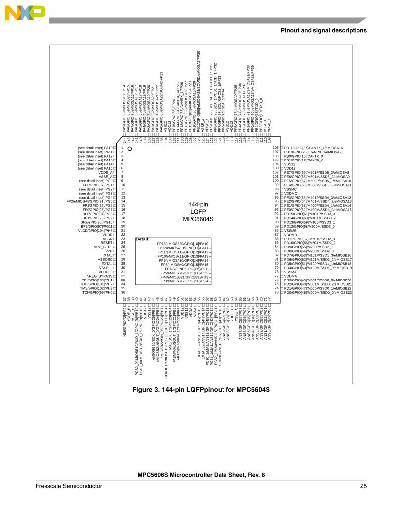
Figure 3. 144-pin LQFPpinout for MPC5604S
37 38 39 40 41 42 43 44 45 46 47 48 49 50 51 52 53 54 55 56 57 58 59 60 61 62 63 64 65 66 67 68 69 70 71 72
123456789101112131415161718192021222324252627282930313233343536
108107106105104103102101100
999897969594939291908988878685848382818079787776757473
144
143
142
141
140
139
138
137
136
135
134
133
132
131
130
129
128
127
126
125
124
123
122
121
120
119
118
117
116
115
114
113
112
111
110
109
NM
I/GP
IO[7
2]/P
F2
VD
DE
_B
VS
SE
_B
PC
S2_
0/eM
IOS
B19
/RX
D_1
/GP
IO[2
8]/P
B12
PC
S1_
0/eM
IOS
B18
/TX
D_1
/GP
IO[2
9]/P
B13
VD
D1
2V
SS
12
eMIO
SB
20/S
CK
_0/
GP
IO[2
5]/P
B9
eM
IOS
B2
1/S
OU
T_
0/G
PIO
[24
]/P
B8
eMIO
SB
22/S
IN_
0/G
PIO
[23]
/PB
7C
LKO
UT
/eM
IOS
B16
/PC
S0
_0/G
PIO
[103
]/PH
4M
A0/
SC
K_
1/G
PIO
[20]
/PB
4F
AB
M/M
A1/
SO
UT
_1/
GP
IO[2
1]/P
B5
AB
S[0
]/MA
2/S
IN_
1/G
PIO
[22
]/P
B6
VD
D1
2V
SS
12
VD
DA
VS
SA
XTA
L32
/AN
S15
/GP
IO[4
5]/P
C15
EX
TAL
32/A
NS
14/
GP
IO[4
4]/P
C14
PC
S0_
1/M
A2
/AN
S13
/GP
IO[4
3]/P
C13
PC
S1_
1/M
A1
/AN
S12
/GP
IO[4
2]/P
C12
PC
S2_
1/M
A0/
AN
S11
/GP
IO[4
1]/P
C11
SO
UN
D/A
NS
10
(mux
)/G
PIO
[40]
/PC
10
AN
S9
/GP
IO[3
9]/P
C9
AN
S8
/GP
IO[3
8]/P
C8
VD
DE
_C
VS
SE
_C
AN
S7
/GP
IO[3
7]/P
C7
AN
S6
/GP
IO[3
6]/P
C6
AN
S5
/GP
IO[3
5]/P
C5
AN
S4
/GP
IO[3
4]/P
C4
AN
S3
/GP
IO[3
3]/P
C3
AN
S2
/GP
IO[3
2]/P
C2
AN
S1
/GP
IO[3
1]/P
C1
AN
S0
/GP
IO[3
0]/P
C0
PA
9/G
PIO
[9]/e
MIO
SB
18/F
P14
PA
8/G
PIO
[8]/e
MIO
SB
23/F
P15
PA
7/G
PIO
[7]/e
MIO
SA
16/F
P16
PA
6/G
PIO
[6]/e
MIO
SA
15/F
P17
PA
5/G
PIO
[5]/e
MIO
SA
17/F
P18
PA
4/G
PIO
[4]/e
MIO
SA
18/F
P19
PA
3/G
PIO
[3]/e
MIO
SA
19/F
P20
PA
2/G
PIO
[2]/e
MIO
SA
20/F
P21
PA
1/G
PIO
[1]/e
MIO
SA
21/F
P22
PA
0/G
PIO
[0]/e
MIO
SA
22
/SO
UN
D/F
P2
3V
SS
12
VD
D12
PF
15/G
PIO
[85]
/FP
24P
F14
/GP
IO[8
4]/C
AN
TX
_1/F
P25
PF
13/G
PIO
[83]
/CA
NR
X_1
/FP
26P
F12
/GP
IO[8
2]/e
MIO
SB
16/F
P27
PF
11/G
PIO
[81]
/eM
IOS
B23
/FP
28P
F10
/GP
IO[8
0]/e
MIO
SA
16/F
P29
PG
12/
GP
IO[9
8]/e
MIO
SA
23
/SO
UN
D/e
MIO
SA
8/F
P3
0V
SS
E_
AV
DD
E_
AP
F9/
GP
IO[7
9]/S
CL_
1/P
CS
1_0/
TX
D_1
/FP
31P
F8/
GP
IO[7
8]/S
DA
_1/P
CS
1_1
/RX
D_1
/FP
32P
F7/
GP
IO[7
7]/S
CL_
0/P
CS
2_1/
FP
33P
F6/
GP
IO[7
6]/S
DA
_0/F
P34
VS
S1
2V
DD
12P
F5/
GP
IO[7
5]/e
MIO
SA
9/F
P35
PF
4/G
PIO
[74]
/eM
IOS
A10
/FP
36P
F3/
GP
IO[7
3]/e
MIO
SA
11/F
P37
PF
1/G
PIO
[71]
/eM
IOS
A12
/eM
IOS
A2
1/F
P38
PF
0/G
PIO
[70]
/eM
IOS
A13
/eM
IOS
A2
2/F
P39
PB
2/G
PIO
[18
]/TX
D_
0P
B3
/GP
IO[1
9]/R
XD
_0
VS
SE
_E
VD
DE
_E
PB11/GPIO[27]/CANTX_1/eMIOSA16PB10GPIO[26]//CANRX_1/eMIOSA23PB0/GPIO[16]/CANTX_0PB1/GPIO[17]/CANRX_0VSS12VDD12PE7/GPIO[69]/M5C1P/SSD5_3/eMIOSA8PE6/GPIO[68]/M5C1M/SSD5_2/eMIOSA9PE5/GPIO[67]/M5C0P/SSD5_1/eMIOSA10PE4/GPIO[66]/M5C0M/SSD5_0/eMIOSA11VSSMCVDDMCPE3/GPIO[65]/M4C1P/SSD4_3/eMIOSA12PE2/GPIO[64]/M4C1M/SSD4_2/eMIOSA13PE1/GPIO[63]/M4C0P/SSD4_1/eMIOSA14PE0/GPIO[62]/M4C0M/SSD4_0/eMIOSA15PD15/GPIO[61]/M3C1P/SSD3_3PD14/GPIO[60]/M3C1M/SSD3_2PD13/GPIO[59]/M3C0P/SSD3_1PD12/GPIO[58/M3C0M/SSD3_0VSSMBVDDMBPD11/GPIO[57]/M2C1P/SSD2_3PD10/GPIO[56]/M2C1M/SSD2_2PD9/GPIO[55]/M2C0P/SSD2_1PD8/GPIO[54]/M2C0M/SSD2_0PD7/GPIO[53]/M1C1P/SSD1_3/eMIOSB16PD6/GPIO[52]/M1C1M/SSD1_2/eMIOSB17PD5/GPIO[51]/M1C0P/SSD1_1/eMIOSB18PD4/GPIO[50]/M1C0M/SSD1_0/eMIOSB19VSSMAVDDMAPD3/GPIO[49]/M0C1P/SSD0_3/eMIOSB20PD2/GPIO[48]/M0C1M/SSD0_2/eMIOSB21PD1/GPIO[47]/M0C0P/SSD0_1/eMIOSB22PD0/GPIO[46]/M0C0M/SSD0_0/eMIOSB23
(see detail inset) PA10(see detail inset) PA11(see detail inset) PA12(see detail inset) PA13(see detail inset) PA14(see detail inset) PA15
VDDE_AVSSE_A
(see detail inset) PG0FP6/GPIO[87]/PG1
(see detail inset) PG2(see detail inset) PG3(see detail inset) PG4
FP2/eMIOSA8/GPIO[91]/PG5FP1/GPIO[92]/PG6FP0/GPIO[93]/PG7BP0/GPIO[94]/PG8BP1/GPIO[95]/PG9
BP2/GPIO[96]/PG10BP3/GPIO[97]/PG11
VLCD/GPIO[104]/PH5VDDRVSSR
RESETVRC_CTRL
VPPXTAL
VSSOSCEXTAL
VSSPLLVDDPLL
VREG_BYPASSTDI/GPIO[100]/PH1
TDO/GPIO[101]/PH2TMS/GPIO[102]/PH3
TCK/GPIO[99]/PH0
Detail:FP13/eMIOSB20/GPIO[10]/PA10 –FP12/eMIOSA13/GPIO[11]/PA11 –FP11/eMIOSA12/GPIO[12]/PA12 –FP10/eMIOSA11/GPIO[13]/PA13 –FP9/eMIOSA10/GPIO[14]/PA14 –
FP8/eMIOSA9/GPIO[15]/PA15 –FP7/SOUND/GPIO[86]/PG0 –
FP5/eMIOSB19/GPIO[88]/PG2 –FP4/eMIOSB21/GPIO[89]/PG3 –FP3/eMIOSB17/GPIO[90]/PG4 –
144-pinLQFP
MPC5604S
MPC5606S Microcontroller Data Sheet, Rev. 8
Pinout and signal descriptions
Freescale Semiconductor26
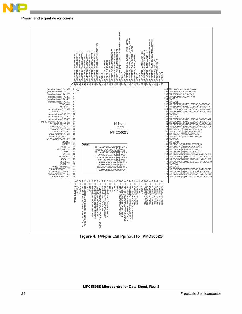
Figure 4. 144-pin LQFPpinout for MPC5602S
37 38 39 40 41 42 43 44 45 46 47 48 49 50 51 52 53 54 55 56 57 58 59 60 61 62 63 64 65 66 67 68 69 70 71 72
123456789101112131415161718192021222324252627282930313233343536
108107106105104103102101100
999897969594939291908988878685848382818079787776757473
144
143
142
141
140
139
138
137
136
135
134
133
132
131
130
129
128
127
126
125
124
123
122
121
120
119
118
117
116
115
114
113
112
111
110
109
NM
I/GP
IO[7
2]/P
F2
VD
DE
_B
VS
SE
_B
PC
S2_
0/eM
IOS
B19
/RX
D_1
/GP
IO[2
8]/P
B12
PC
S1_
0/eM
IOS
B18
/TX
D_1
/GP
IO[2
9]/P
B13
VD
D1
2V
SS
12
eMIO
SB
20/S
CK
_0/
GP
IO[2
5]/P
B9
eM
IOS
B2
1/S
OU
T_
0/G
PIO
[24
]/P
B8
eMIO
SB
22/S
IN_
0/G
PIO
[23]
/PB
7C
LKO
UT
/eM
IOS
B16
/PC
S0
_0/G
PIO
[103
]/PH
4M
A0/
SC
K_
1/G
PIO
[20]
/PB
4F
AB
M/M
A1/
SO
UT
_1/
GP
IO[2
1]/P
B5
AB
S[0
]/MA
2/S
IN_
1/G
PIO
[22
]/P
B6
VD
D1
2V
SS
12
VD
DA
VS
SA
XTA
L32
/AN
S15
/GP
IO[4
5]/P
C15
EX
TAL
32/A
NS
14/
GP
IO[4
4]/P
C14
PC
S0_
1/M
A2
/AN
S13
/GP
IO[4
3]/P
C13
PC
S1_
1/M
A1
/AN
S12
/GP
IO[4
2]/P
C12
PC
S2_
1/M
A0/
AN
S11
/GP
IO[4
1]/P
C11
SO
UN
D/A
NS
10
(mux
)/G
PIO
[40]
/PC
10
AN
S9
/GP
IO[3
9]/P
C9
AN
S8
/GP
IO[3
8]/P
C8
VD
DE
_C
VS
SE
_C
AN
S7
/GP
IO[3
7]/P
C7
AN
S6
/GP
IO[3
6]/P
C6
AN
S5
/GP
IO[3
5]/P
C5
AN
S4
/GP
IO[3
4]/P
C4
AN
S3
/GP
IO[3
3]/P
C3
AN
S2
/GP
IO[3
2]/P
C2
AN
S1
/GP
IO[3
1]/P
C1
AN
S0
/GP
IO[3
0]/P
C0
PA
9/G
PIO
[9]/e
MIO
SB
18/F
P14
PA
8/G
PIO
[8]/e
MIO
SB
23/F
P15
PA
7/G
PIO
[7]/e
MIO
SA
16/F
P16
PA
6/G
PIO
[6]/e
MIO
SA
15/F
P17
PA
5/G
PIO
[5]/e
MIO
SA
17/F
P18
PA
4/G
PIO
[4]/e
MIO
SA
18/F
P19
PA
3/G
PIO
[3]/e
MIO
SA
19/F
P20
PA
2/G
PIO
[2]/e
MIO
SA
20/F
P21
PA
1/G
PIO
[1]/e
MIO
SA
21/F
P22
PA
0/G
PIO
[0]/e
MIO
SA
22
/SO
UN
D/F
P2
3V
SS
12
VD
D12
PF
15/G
PIO
[85]
/FP
24P
F14
/GP
IO[8
4]/F
P25
PF
13/G
PIO
[83]
/FP
26P
F12
/GP
IO[8
2]/e
MIO
SB
16/F
P27
PF
11/G
PIO
[81]
/eM
IOS
B23
/FP
28P
F10
/GP
IO[8
0]/e
MIO
SA
16/F
P29
PG
12/
GP
IO[9
8]/e
MIO
SA
23
/SO
UN
D/e
MIO
SA
8/F
P3
0V
SS
E_
AV
DD
E_
AP
F9/
GP
IO[7
9]/S
CL_
1/P
CS
1_0/
TX
D_1
/FP
31P
F8/
GP
IO[7
8]/S
DA
_1/P
CS
1_1
/RX
D_1
/FP
32P
F7/
GP
IO[7
7]/S
CL_
0/P
CS
2_1/
FP
33P
F6/
GP
IO[7
6]/S
DA
_0/F
P34
VS
S1
2V
DD
12P
F5/
GP
IO[7
5]/e
MIO
SA
9/F
P35
PF
4/G
PIO
[74]
/eM
IOS
A10
/FP
36P
F3/
GP
IO[7
3]/e
MIO
SA
11/F
P37
PF
1/G
PIO
[71]
/eM
IOS
A12
/eM
IOS
A2
1/F
P38
PF
0/G
PIO
[70]
/eM
IOS
A13
/eM
IOS
A2
2/F
P39
PB
2/G
PIO
[18
]/TX
D_
0P
B3
/GP
IO[1
9]/R
XD
_0
VS
SE
_E
VD
DE
_E
PB11/GPIO[27]/eMIOSA16PB10GPIO[26]/eMIOSA23PB0/GPIO[16]/CANTX_0PB1/GPIO[17]/CANRX_0VSS12VDD12PE7/GPIO[69]/M5C1P/SSD5_3/eMIOSA8PE6/GPIO[68]/M5C1M/SSD5_2/eMIOSA9PE5/GPIO[67]/M5C0P/SSD5_1/eMIOSA10PE4/GPIO[66]/M5C0M/SSD5_0/eMIOSA11VSSMCVDDMCPE3/GPIO[65]/M4C1P/SSD4_3/eMIOSA12PE2/GPIO[64]/M4C1M/SSD4_2/eMIOSA13PE1/GPIO[63]/M4C0P/SSD4_1/eMIOSA14PE0/GPIO[62]/M4C0M/SSD4_0/eMIOSA15PD15/GPIO[61]/M3C1P/SSD3_3PD14/GPIO[60]/M3C1M/SSD3_2PD13/GPIO[59]/M3C0P/SSD3_1PD12/GPIO[58/M3C0M/SSD3_0VSSMBVDDMBPD11/GPIO[57]/M2C1P/SSD2_3PD10/GPIO[56]/M2C1M/SSD2_2PD9/GPIO[55]/M2C0P/SSD2_1PD8/GPIO[54]/M2C0M/SSD2_0PD7/GPIO[53]/M1C1P/SSD1_3/eMIOSB16PD6/GPIO[52]/M1C1M/SSD1_2/eMIOSB17PD5/GPIO[51]/M1C0P/SSD1_1/eMIOSB18PD4/GPIO[50]/M1C0M/SSD1_0/eMIOSB19VSSMAVDDMAPD3/GPIO[49]/M0C1P/SSD0_3/eMIOSB20PD2/GPIO[48]/M0C1M/SSD0_2/eMIOSB21PD1/GPIO[47]/M0C0P/SSD0_1/eMIOSB22PD0/GPIO[46]/M0C0M/SSD0_0/eMIOSB23
(see detail inset) PA10(see detail inset) PA11(see detail inset) PA12(see detail inset) PA13(see detail inset) PA14(see detail inset) PA15
VDDE_AVSSE_A
(see detail inset) PG0FP6/GPIO[87]/PG1
(see detail inset) PG2(see detail inset) PG3(see detail inset) PG4
FP2/eMIOSA8/GPIO[91]/PG5FP1/GPIO[92]/PG6FP0/GPIO[93]/PG7BP0/GPIO[94]/PG8BP1/GPIO[95]/PG9
BP2/GPIO[96]/PG10BP3/GPIO[97]/PG11
VLCD/GPIO[104]/PH5VDDRVSSR
RESETVRC_CTRL
VPPXTAL
VSSOSCEXTAL
VSSPLLVDDPLL
VREG_BYPASSTDI/GPIO[100]/PH1
TDO/GPIO[101]/PH2TMS/GPIO[102]/PH3
TCK/GPIO[99]/PH0
Detail:FP13/eMIOSB20/GPIO[10]/PA10 –FP12/eMIOSA13/GPIO[11]/PA11 –FP11/eMIOSA12/GPIO[12]/PA12 –FP10/eMIOSA11/GPIO[13]/PA13 –FP9/eMIOSA10/GPIO[14]/PA14 –
FP8/eMIOSA9/GPIO[15]/PA15 –FP7/SOUND/GPIO[86]/PG0 –
FP5/eMIOSB19/GPIO[88]/PG2 –FP4/eMIOSB21/GPIO[89]/PG3 –FP3/eMIOSB17/GPIO[90]/PG4 –
144-pinLQFP
MPC5602S
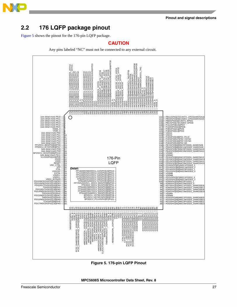
Pinout and signal descriptions
MPC5606S Microcontroller Data Sheet, Rev. 8
Freescale Semiconductor 27
2.2 176 LQFP package pinoutFigure 5 shows the pinout for the 176-pin LQFP package.
CAUTIONAny pins labeled “NC” must not be connected to any external circuit.
Figure 5. 176-pin LQFP Pinout
176-PinLQFP
1234567891011121314151617181920212223242526272829303132333435363738394041424344
176
175
174
173
172
171
170
169
168
167
166
165
164
163
162
161
160
159
158
157
156
155
154
153
152
151
150
149
148
147
146
145
144
143
142
141
140
139
138
137
136
135
134
133
45
46
47
48
49
50
51
52
53
54
55
56
57
58
59
60
61
62
63
64
65
66
67
68
69
70
71
72
73
74
75
76
77
78
79
80
81
82
83
84
85
86
87
88
132131130129128127126125124123122121120119118117116115114113112111110109108107106105104103102101100
9998979695949392919089
PA
9/G
PIO
[9]/
DC
U_G
1/eM
IOS
B18
/SD
A_2
/FP
14P
A8
/GP
IO[8
]/D
CU
_G0/
eMIO
SB
23/S
CL_
2/F
P15
PA
7/G
PIO
[7]/
DC
U_R
7/eM
IOS
A16
/FP
16
PA
6/G
PIO
[6]/
DC
U_R
6/eM
IOS
A15
/FP
17
PA
5/G
PIO
[5]/
DC
U_R
5/eM
IOS
A17
/FP
18
VS
SE
_AV
DD
E_A
PA
4/G
PIO
[4]/
DC
U_R
4/eM
IOS
A18
/FP
19
PA
3/G
PIO
[3]/
DC
U_R
3/eM
IOS
A19
/FP
20
PA
2/G
PIO
[2]/
DC
U_R
2/eM
IOS
A20
/FP
21
PA
1/G
PIO
[1]/
DC
U_R
1/eM
IOS
A21
/FP
22
PA
0/G
PIO
[0]/
DC
U_R
0/eM
IOS
A22
/SO
UN
D/F
P23
VS
S12
VD
D12
PF
15/G
PIO
[85]
/SC
K_2
/FP
24P
F1
4/G
PIO
[84
]/S
OU
T_
2/C
AN
TX
_1
/FP
25
PF
13/G
PIO
[83]
/SIN
_2/C
AN
RX
_1/F
P2
6P
F12
/GP
IO[8
2]/e
MIO
SB
16/P
CS
2_2/
FP
27P
F11
/GP
IO[8
1]/e
MIO
SB
23/P
CS
1_2/
FP
28P
F10
/GP
IO[8
0]/e
MIO
SA
16/P
CS
0_2/
FP
29P
G1
2/G
PIO
[98]
/eM
IOS
A23
/SO
UN
D/e
MIO
SA
8/F
P30
VS
SE
_AV
DD
E_A
PF
9/G
PIO
[79]
/SC
L_1/
PC
S0_
1/T
XD
_1/F
P31
PF
8/G
PIO
[78]
/SD
A_
1/P
CS
1_1
/RX
D_1
/FP
32P
F7/
GP
IO[7
7]/S
CL_
0/P
CS
2_1/
FP
33P
F6/
GP
IO[7
6]/S
DA
_0/
FP
34V
SS
12V
DD
12P
F5/
GP
IO[7
5]/e
MIO
SA
9/D
CU
_TA
G/F
P35
PF
4/G
PIO
[74]
/eM
IOS
A1
0/P
DI7
/FP
36P
F3/
GP
IO[7
3]/e
MIO
SA
11/P
DI6
/FP
37P
F1/
GP
IO[7
1]/e
MIO
SA
12/
PD
I5/e
MIO
SA
21/F
P38
PF
0/G
PIO
[70]
/eM
IOS
A1
3/P
DI4
/eM
IOS
A22
/FP
39P
K1/
GP
IO[1
22]/
PD
I13/
eMIO
SA
17P
K0/
GP
IO[1
21]/
PD
I12/
eMIO
SA
18/D
CU
_TA
GP
B2/
GP
IO[1
8]/T
XD
_0
PB
3/G
PIO
[19]
/RX
D_0
PJ1
5/G
PIO
[120
]/P
DI1
1/eM
IOS
A19
PJ1
4/G
PIO
[119
]/P
DI1
0/eM
IOS
A20
PJ1
3/G
PIO
[118
]/P
DI9
/eM
IOS
B20
PJ1
2/G
PIO
[117
]/P
DI8
/eM
IOS
B17
VS
SE
_EV
DD
E_E
NM
I/G
PIO
[72]
/PF
2V
DD
E_B
VS
SE
_BP
CS
2_0/
eMIO
SB
19/R
XD
_1/
GP
IO[2
8]/P
B12
PC
S1_
0/eM
IOS
B18
/TX
D_
1/G
PIO
[29]
/PB
13V
DD
12
VS
S12
eMIO
SA
15/S
DA
_1/G
PIO
[131
]/P
K10
eMIO
SA
14/S
CL_
1/G
PIO
[132
]/P
K11
eMIO
SB
20/S
CK
_0/G
PIO
[25]
/PB
9eM
IOS
B21
/SO
UT
_0/G
PIO
[24]
/PB
8eM
IOS
B22
/SIN
_0/G
PIO
[23]
/PB
7C
AN
RX
_0/P
DI0
/GP
IO[1
09]
/PJ4
CA
NT
X_0
/PD
I1/G
PIO
[11
0]/P
J5eM
IOS
A22
/CA
NR
X_
1/P
DI2
/GP
IO[1
11]/
PJ6
eMIO
SA
21/C
AN
TX
_1/P
DI3
/GP
IO[1
12]
/PJ7
CLK
OU
T/e
MIO
SB
16/P
CS
0_0/
GP
IO[1
03]/
PH
4M
A0/
SC
K_1
/GP
IO[2
0]/P
B4
FA
BM
/MA
1/S
OU
T_1
/GP
IO[2
1]/P
B5
VD
DE
_BV
SS
E_
BA
BS
[0]/
MA
2/S
IN_1
/GP
IO[2
2]/P
B6
VD
D12
VS
S12
VD
DA
VS
SA
XTA
L32/
AN
S15
/GP
IO[4
5]/P
C15
EX
TAL3
2/A
NS
14/G
PIO
[44]
/PC
14P
CS
0_1/
MA
2/A
NS
13/G
PIO
[43]
/PC
13P
CS
1_1/
MA
1/A
NS
12/G
PIO
[42]
/PC
12P
CS
2_1/
MA
0/A
NS
11/G
PIO
[41]
/PC
11S
OU
ND
/AN
S10
(mux
)/G
PIO
[40]
/PC
10
AN
S9/
GP
IO[3
9]/P
C9
AN
S8/
GP
IO[3
8]/P
C8
VD
DE
_CV
SS
E_C
AN
S7/
GP
IO[3
7]/P
C7
AN
S6/
GP
IO[3
6]/P
C6
AN
S5/
GP
IO[3
5]/P
C5
AN
S4/
GP
IO[3
4]/P
C4
AN
S3/
GP
IO[3
3]/P
C3
AN
S2/
GP
IO[3
2]/P
C2
AN
S1/
GP
IO[3
1]/P
C1
AN
S0/
GP
IO[3
0]/P
C0
PB11/GPIO[27]/CANTX_1/PDI3/eMIOSA16PB10/GPIO[26]/CANRX_1/PDI2/eMIOSA23PB0/GPIO[16]/CANTX_0/PDI1PB1/GPIO[17]/CANRX_0/PDI0PJ11/GPIO[116]/PDI7PJ10/GPIO[115]/PDI6PJ9/GPIO[114]/PDI5PJ8/GPIO[113]/PDI4VSS12VDD12PJ3/GPIO[108]/PDI_PCLKPJ2/GPIO[107]/PDI_VSYNCPJ1/GPIO[106]/PDI_HSYNCPJ0/GPIO[105]/PDI_DEPE7/GPIO[69]/M5C1P/SSD5_3/eMIOSA8PE6/GPIO[68]/M5C1M/SSD5_2/eMIOSA9PE5/GPIO[67]/M5C0P/SSD5_1/eMIOSA10PE4/GPIO[66]/M5C0M/SSD5_0/eMIOSA11VSSMCVDDMCPE3/GPIO[65]/M4C1P/SSD4_3/eMIOSA12PE2/GPIO[64]/M4C1M/SSD4_2/eMIOSA13PE1/GPIO[63]/M4C0P/SSD4_1/eMIOSA14PE0/GPIO[62]/M4C0M/SSD4_0/eMIOSA15PD15/GPIO[61]/M3C1P/SSD3_3PD14/GPIO[60]/M3C1M/SSD3_2PD13/GPIO[59]/M3C0P/SSD3_1PD12/GPIO[58]/M3C0M/SSD3_0VSSMBVDDMBPD11/GPIO[57]/M2C1P/SSD2_3PD10/GPIO[56]/M2C1M/SSD2_2PD9/GPIO[55]/M2C0P/SSD2_1PD8/GPIO[54]/M2C0M/SSD2_0PD7/GPIO[53]/M1C1P/SSD1_3/eMIOSB16PD6/GPIO[52]/M1C1M/SSD1_2/eMIOSB17PD5/GPIO[51]/M1C0P/SSD1_1/eMIOSB18PD4/GPIO[50]/M1C0M/SSD1_0/eMIOSB19VSSMAVDDMAPD3/GPIO[49]/M0C1P/SSD0_3/eMIOSB20PD2/GPIO[48]/M0C1M/SSD0_2/eMIOSB21PD1/GPIO[47]/M0C0P/SSD0_1/eMIOSB22PD0/GPIO[46]/M0C0M/SSD0_0/eMIOSB23
(see detail inset) PA10(see detail inset) PA11(see detail inset) PA12(see detail inset) PA13(see detail inset) PA14(see detail inset) PA15
VDDE_AVSSE_A
(see detail inset) PG0(see detail inset) PG1(see detail inset) PG2(see detail inset) PG3(see detail inset) PG4(see detail inset) PG5
FP1/DCU_B6/GPIO[92]/PG6FP0/DCU_B7/GPIO[93]/PG7
(see detail inset) PG8(see detail inset) PG9
BP2/DCU_DE/GPIO[96]/PG10(see detail inset) PG11VLCD/GPIO[104]/PH5
VDDRVSSR
RESETVRC_CTRL
VPPXTAL
VSSOSCEXTAL
VSSPLLVDDPLL
VREG_BYPASSPDI10/MCKO/GPIO[123]/PK2PDI11/MSEO/GPIO[124]/PK3PDI12/EVTO/GPIO[125]/PK4
TDI/GPIO[100]/PH1PDI13/EVTI/GPIO[126]/PK5
PDI14/MDO0/GPIO[127]/PK6TDO/GPIO[101]/PH2
PDI15/MDO1/GPIO[128]/PK7TMS/GPIO[102]/PH3
PDI16/MDO2/GPIO[129]/PK8TCK/GPIO[99]/PH0
PDI17/MDO3/GPIO[130]/PK9
Detail:FP13/eMIOSB20/DCU_G2/GPIO[10]/PA10 –FP12/eMIOSA13/DCU_G3/GPIO[11]/PA11 –FP11/eMIOSA12/DCU_G4/GPIO[12]/PA12 –FP10/eMIOSA11/DCU_G5/GPIO[13]/PA13 –FP9/eMIOSA10/DCU_G6/GPIO[14]/PA14 –
FP8/eMIOSA9/DCU_G7/GPIO[15]/PA15 –FP7/SOUND/SCL_3/DCU_B0/GPIO[86]/PG0 –
FP6/SDA_3/DCU_B1/GPIO[87]/PG1 –FP5/eMIOSB19/DCU_B2/GPIO[88]/PG2 –FP4/eMIOSB21/DCU_B3/GPIO[89]/PG3 –FP3/eMIOSB17/DCU_B4/GPIO[90]/PG4 –
FP2/eMIOSA8/DCU_B5/GPIO[91]/PG5 –BP0/DCU_VSYNC/GPIO[94]/PG8 –BP1/DCU_HSYNC/GPIO[95]/PG9 –BP3/DCU_PCLK/GPIO[97]/PG11 –
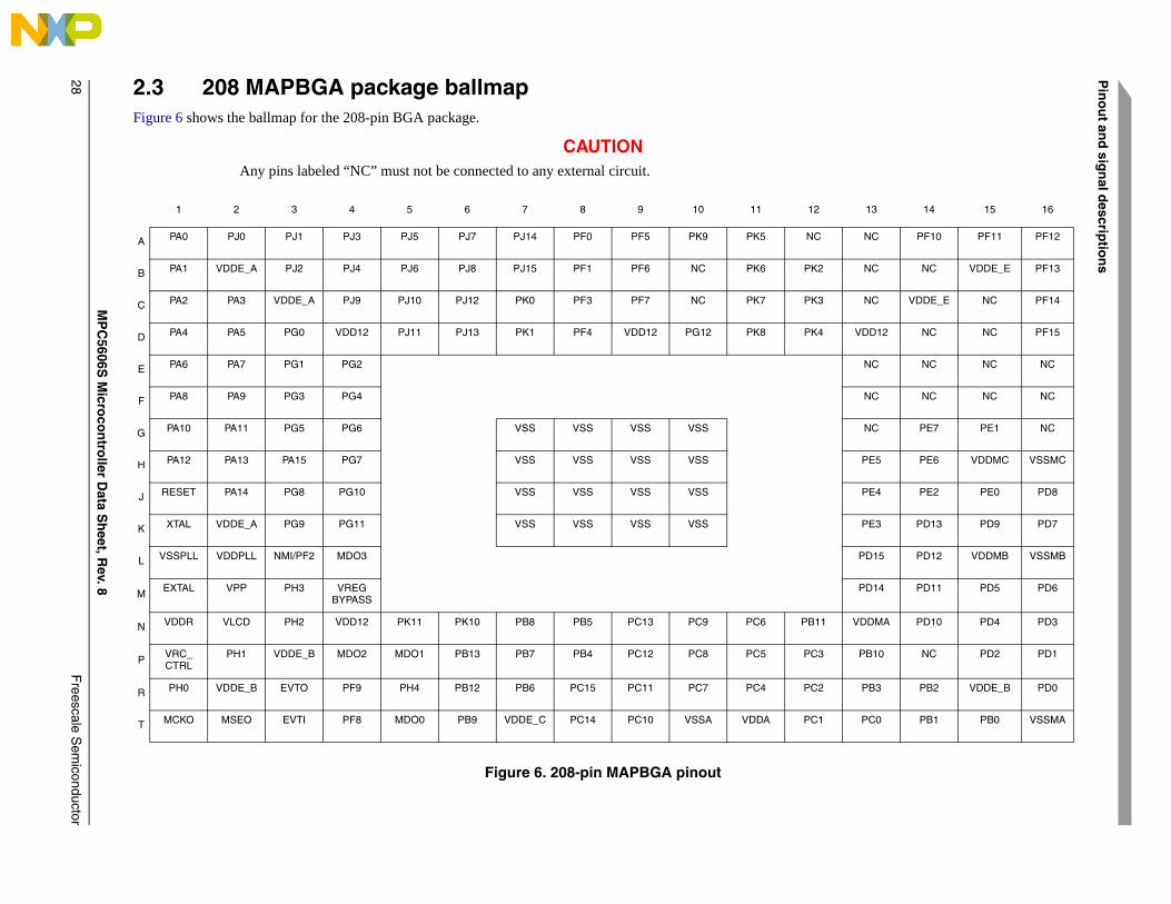
MP
C5606S
Micro
con
troller D
ata Sh
eet, Rev. 8
Pin
ou
t and
sign
al descrip
tion
s
Freescale S
emiconductor
28 2.3 208 MAPBGA package ballmapFigure 6 shows the ballmap for the 208-pin BGA package.
CAUTIONAny pins labeled “NC” must not be connected to any external circuit.
Figure 6. 208-pin MAPBGA pinout
1 2 3 4 5 6 7 8 9 10 11 12 13 14 15 16
A PA0 PJ0 PJ1 PJ3 PJ5 PJ7 PJ14 PF0 PF5 PK9 PK5 NC NC PF10 PF11 PF12
B PA1 VDDE_A PJ2 PJ4 PJ6 PJ8 PJ15 PF1 PF6 NC PK6 PK2 NC NC VDDE_E PF13
C PA2 PA3 VDDE_A PJ9 PJ10 PJ12 PK0 PF3 PF7 NC PK7 PK3 NC VDDE_E NC PF14
D PA4 PA5 PG0 VDD12 PJ11 PJ13 PK1 PF4 VDD12 PG12 PK8 PK4 VDD12 NC NC PF15
E PA6 PA7 PG1 PG2 NC NC NC NC
F PA8 PA9 PG3 PG4 NC NC NC NC
G PA10 PA11 PG5 PG6 VSS VSS VSS VSS NC PE7 PE1 NC
H PA12 PA13 PA15 PG7 VSS VSS VSS VSS PE5 PE6 VDDMC VSSMC
J RESET PA14 PG8 PG10 VSS VSS VSS VSS PE4 PE2 PE0 PD8
K XTAL VDDE_A PG9 PG11 VSS VSS VSS VSS PE3 PD13 PD9 PD7
L VSSPLL VDDPLL NMI/PF2 MDO3 PD15 PD12 VDDMB VSSMB
M EXTAL VPP PH3 VREG BYPASS
PD14 PD11 PD5 PD6
N VDDR VLCD PH2 VDD12 PK11 PK10 PB8 PB5 PC13 PC9 PC6 PB11 VDDMA PD10 PD4 PD3
P VRC_CTRL
PH1 VDDE_B MDO2 MDO1 PB13 PB7 PB4 PC12 PC8 PC5 PC3 PB10 NC PD2 PD1
R PH0 VDDE_B EVTO PF9 PH4 PB12 PB6 PC15 PC11 PC7 PC4 PC2 PB3 PB2 VDDE_B PD0
T MCKO MSEO EVTI PF8 MDO0 PB9 VDDE_C PC14 PC10 VSSA VDDA PC1 PC0 PB1 PB0 VSSMA
Pinout and signal descriptions
MPC5606S Microcontroller Data Sheet, Rev. 8
Freescale Semiconductor 29
2.4 Pad configuration during reset phasesAll pads have a fixed configuration under reset.
During the startup phase, all pads are forced to tristate.
After startup phase, all pads are floating with the following exceptions:
• PB[5] (FAB) is pulldown. Without external strong pullup the device starts fetching from flash.
• RESET pad is driven low. This is released only after PHASE2 reset completion.
• Main oscillator pads (EXTAL, XTAL) are tristate.
• Nexus output pads (MDO[n], MCKO, EVTO, MSEO) are forced to output.
• The following pads are pullup:
— PB[6]
— PH[0]
— PH[1]
— PH[3]
— EVTI
2.5 Voltage supply pinsVoltage supply pins are used to provide power to the device. Two dedicated pins are used for 1.2 V regulator stabilization.
There is a preferred startup sequence for devices in the MPC5606S family. That sequence is described in the next paragraphs.
Broadly, the supply voltages can be grouped as follows:
• VREG HV supply (VDDR)
• Generic I/O supply
— VDDA
— VDDE_A
— VDDE_B
— VDDE_C
— VDDE_E
— VDDMA
— VDDMB
— VDDMC
— VDDPLL
• LV supply (VDD12)
The preferred order of ramp up is as follows:
1. Generic I/O supply
2. VREG HV supply (VDDR should be the last HV supply to ramp up; it is also OK if all HV and generic I/O supplies including VDDR ramp up together)
3. LV supply
The reason for following this sequence is to ensure that when VREG releases its LVDs, the I/O and other HV segments are powered properly. This is important because the MPC5606S does not monitor LVDs on I/O HV supplies.
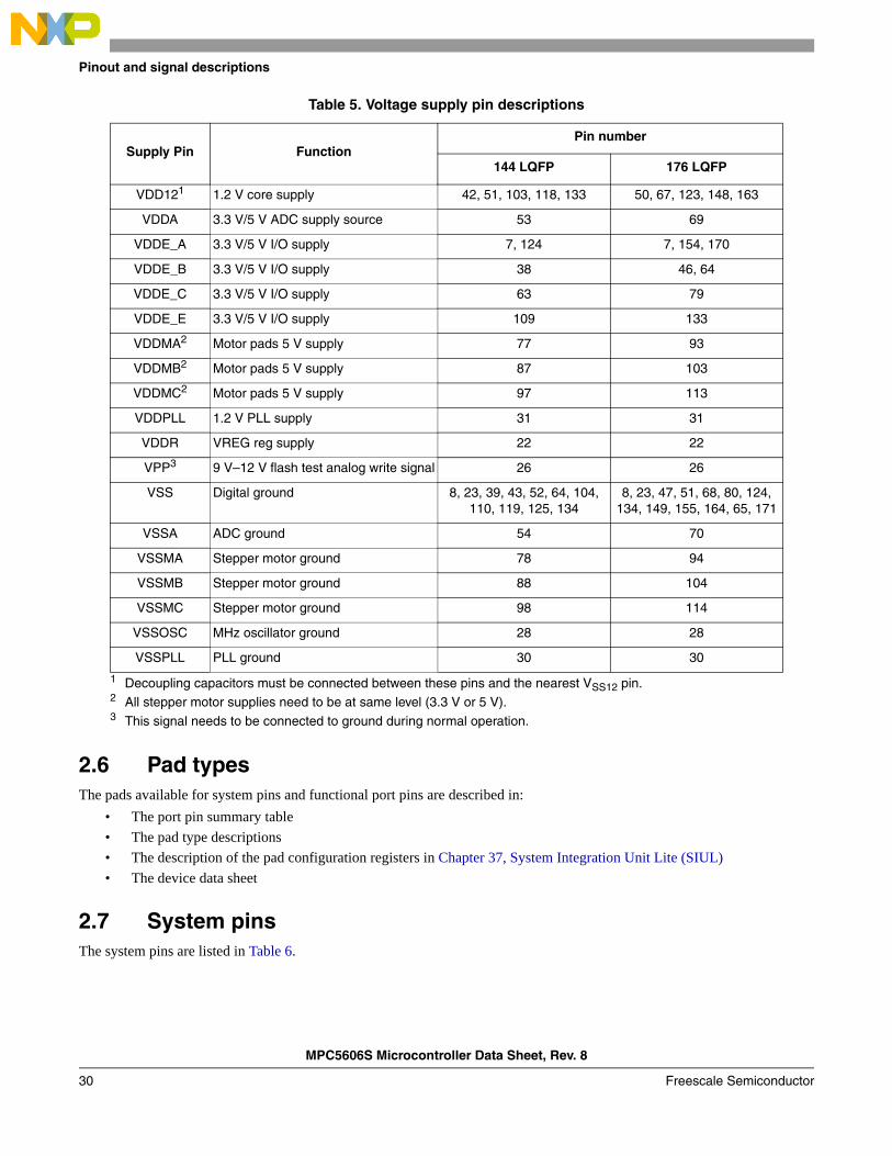
MPC5606S Microcontroller Data Sheet, Rev. 8
Pinout and signal descriptions
Freescale Semiconductor30
2.6 Pad typesThe pads available for system pins and functional port pins are described in:
• The port pin summary table
• The pad type descriptions
• The description of the pad configuration registers in Chapter 37, System Integration Unit Lite (SIUL)
• The device data sheet
2.7 System pinsThe system pins are listed in Table 6.
Table 5. Voltage supply pin descriptions
Supply Pin FunctionPin number
144 LQFP 176 LQFP
VDD121
1 Decoupling capacitors must be connected between these pins and the nearest VSS12 pin.
1.2 V core supply 42, 51, 103, 118, 133 50, 67, 123, 148, 163
VDDA 3.3 V/5 V ADC supply source 53 69
VDDE_A 3.3 V/5 V I/O supply 7, 124 7, 154, 170
VDDE_B 3.3 V/5 V I/O supply 38 46, 64
VDDE_C 3.3 V/5 V I/O supply 63 79
VDDE_E 3.3 V/5 V I/O supply 109 133
VDDMA2
2 All stepper motor supplies need to be at same level (3.3 V or 5 V).
Motor pads 5 V supply 77 93
VDDMB2 Motor pads 5 V supply 87 103
VDDMC2 Motor pads 5 V supply 97 113
VDDPLL 1.2 V PLL supply 31 31
VDDR VREG reg supply 22 22
VPP3
3 This signal needs to be connected to ground during normal operation.
9 V–12 V flash test analog write signal 26 26
VSS Digital ground 8, 23, 39, 43, 52, 64, 104, 110, 119, 125, 134
8, 23, 47, 51, 68, 80, 124, 134, 149, 155, 164, 65, 171
VSSA ADC ground 54 70
VSSMA Stepper motor ground 78 94
VSSMB Stepper motor ground 88 104
VSSMC Stepper motor ground 98 114
VSSOSC MHz oscillator ground 28 28
VSSPLL PLL ground 30 30
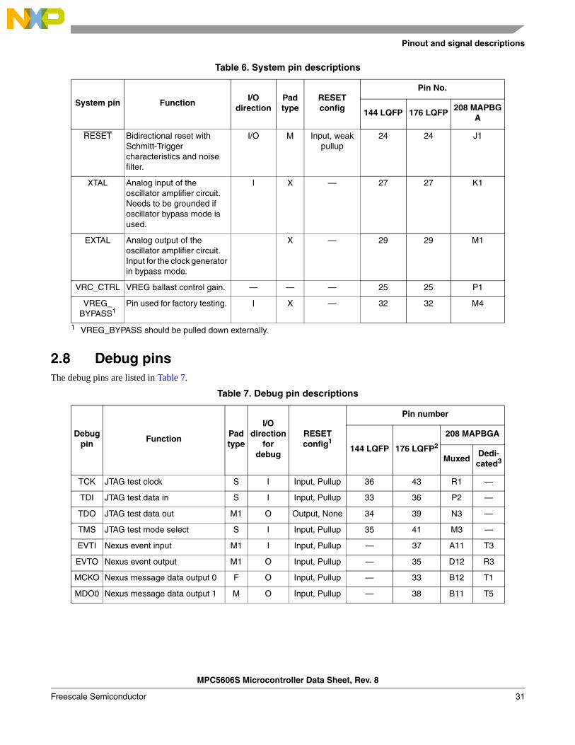
Pinout and signal descriptions
MPC5606S Microcontroller Data Sheet, Rev. 8
Freescale Semiconductor 31
2.8 Debug pinsThe debug pins are listed in Table 7.
Table 6. System pin descriptions
System pin FunctionI/O
directionPad type
RESET config
Pin No.
144 LQFP 176 LQFP208 MAPBG
A
RESET Bidirectional reset with Schmitt-Trigger characteristics and noise filter.
I/O M Input, weak pullup
24 24 J1
XTAL Analog input of the oscillator amplifier circuit. Needs to be grounded if oscillator bypass mode is used.
I X — 27 27 K1
EXTAL Analog output of the oscillator amplifier circuit. Input for the clock generator in bypass mode.
X — 29 29 M1
VRC_CTRL VREG ballast control gain. — — — 25 25 P1
VREG_BYPASS1
1 VREG_BYPASS should be pulled down externally.
Pin used for factory testing. I X — 32 32 M4
Table 7. Debug pin descriptions
Debugpin
FunctionPadtype
I/Odirection
for debug
RESETconfig1
Pin number
144 LQFP 176 LQFP2
208 MAPBGA
MuxedDedi-cated3
TCK JTAG test clock S I Input, Pullup 36 43 R1 —
TDI JTAG test data in S I Input, Pullup 33 36 P2 —
TDO JTAG test data out M1 O Output, None 34 39 N3 —
TMS JTAG test mode select S I Input, Pullup 35 41 M3 —
EVTI Nexus event input M1 I Input, Pullup — 37 A11 T3
EVTO Nexus event output M1 O Input, Pullup — 35 D12 R3
MCKO Nexus message data output 0 F O Input, Pullup — 33 B12 T1
MDO0 Nexus message data output 1 M O Input, Pullup — 38 B11 T5
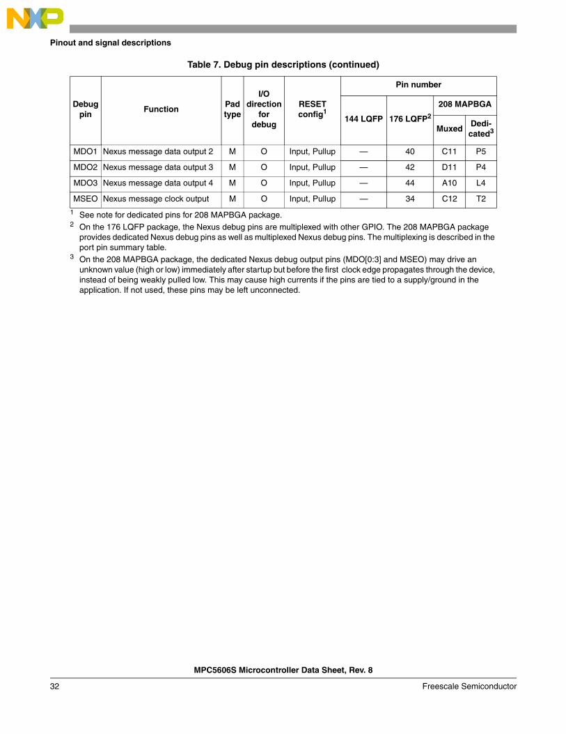
MPC5606S Microcontroller Data Sheet, Rev. 8
Pinout and signal descriptions
Freescale Semiconductor32
MDO1 Nexus message data output 2 M O Input, Pullup — 40 C11 P5
MDO2 Nexus message data output 3 M O Input, Pullup — 42 D11 P4
MDO3 Nexus message data output 4 M O Input, Pullup — 44 A10 L4
MSEO Nexus message clock output M O Input, Pullup — 34 C12 T2
1 See note for dedicated pins for 208 MAPBGA package.2 On the 176 LQFP package, the Nexus debug pins are multiplexed with other GPIO. The 208 MAPBGA package
provides dedicated Nexus debug pins as well as multiplexed Nexus debug pins. The multiplexing is described in the port pin summary table.
3 On the 208 MAPBGA package, the dedicated Nexus debug output pins (MDO[0:3] and MSEO) may drive an unknown value (high or low) immediately after startup but before the first clock edge propagates through the device, instead of being weakly pulled low. This may cause high currents if the pins are tied to a supply/ground in the application. If not used, these pins may be left unconnected.
Table 7. Debug pin descriptions (continued)
Debugpin
FunctionPadtype
I/Odirection
for debug
RESETconfig1
Pin number
144 LQFP 176 LQFP2
208 MAPBGA
MuxedDedi-cated3
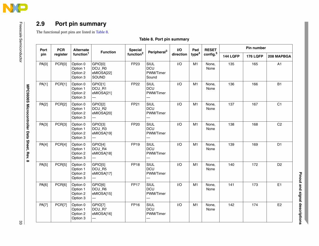
Pin
ou
t and
sign
al descrip
tion
s
MP
C5606S
Micro
con
troller D
ata Sh
eet, Rev. 8
Freescale S
emiconductor
33
2.9 Port pin summaryThe functional port pins are listed in Table 8.
Table 8. Port pin summary
Portpin
PCRregister
Alternatefunction1 Function
Specialfunction2 Peripheral3
I/Odirection
Padtype4
RESETconfig.5
Pin number
144 LQFP 176 LQFP 208 MAPBGA
PA[0] PCR[0] Option 0Option 1Option 2Option 3
GPIO[0]DCU_R0eMIOSA[22]SOUND
FP23 SIULDCUPWM/TimerSound
I/O M1 None, None
135 165 A1
PA[1] PCR[1] Option 0Option 1Option 2Option 3
GPIO[1]DCU_R1eMIOSA[21]—
FP22 SIULDCUPWM/Timer—
I/O M1 None, None
136 166 B1
PA[2] PCR[2] Option 0Option 1Option 2Option 3
GPIO[2]DCU_R2eMIOSA[20]—
FP21 SIULDCUPWM/Timer—
I/O M1 None, None
137 167 C1
PA[3] PCR[3] Option 0Option 1Option 2Option 3
GPIO[3]DCU_R3eMIOSA[19]—
FP20 SIULDCUPWM/Timer—
I/O M1 None, None
138 168 C2
PA[4] PCR[4] Option 0Option 1Option 2Option 3
GPIO[4]DCU_R4eMIOSA[18]—
FP19 SIULDCUPWM/Timer—
I/O M1 None, None
139 169 D1
PA[5] PCR[5] Option 0Option 1Option 2Option 3
GPIO[5]DCU_R5eMIOSA[17]—
FP18 SIULDCUPWM/Timer—
I/O M1 None, None
140 172 D2
PA[6] PCR[6] Option 0Option 1Option 2Option 3
GPIO[6]DCU_R6eMIOSA[15]—
FP17 SIULDCUPWM/Timer—
I/O M1 None, None
141 173 E1
PA[7] PCR[7] Option 0Option 1Option 2Option 3
GPIO[7]DCU_R7eMIOSA[16]—
FP16 SIULDCUPWM/Timer—
I/O M1 None, None
142 174 E2
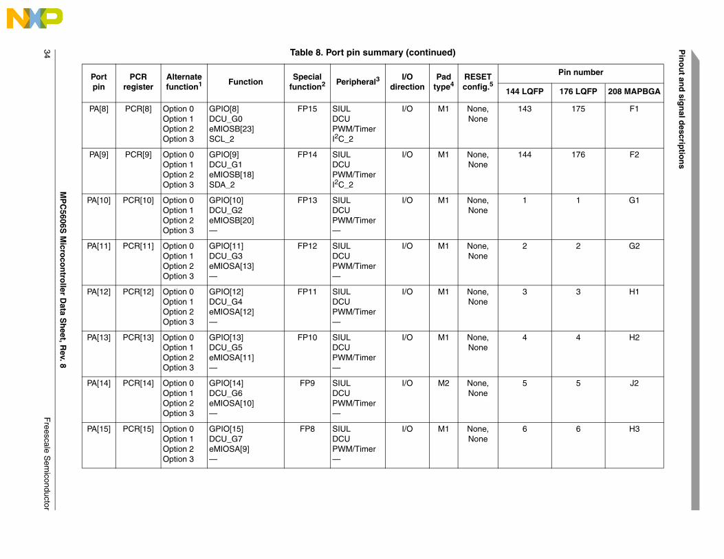
MP
C5606S
Micro
con
troller D
ata Sh
eet, Rev. 8
Pin
ou
t and
sign
al descrip
tion
s
Freescale S
emiconductor
34
PA[8] PCR[8] Option 0Option 1Option 2Option 3
GPIO[8]DCU_G0eMIOSB[23]SCL_2
FP15 SIULDCUPWM/TimerI2C_2
I/O M1 None, None
143 175 F1
PA[9] PCR[9] Option 0Option 1Option 2Option 3
GPIO[9]DCU_G1eMIOSB[18]SDA_2
FP14 SIULDCUPWM/TimerI2C_2
I/O M1 None, None
144 176 F2
PA[10] PCR[10] Option 0Option 1Option 2Option 3
GPIO[10]DCU_G2eMIOSB[20]—
FP13 SIULDCUPWM/Timer—
I/O M1 None, None
1 1 G1
PA[11] PCR[11] Option 0Option 1Option 2Option 3
GPIO[11]DCU_G3eMIOSA[13]—
FP12 SIULDCUPWM/Timer—
I/O M1 None, None
2 2 G2
PA[12] PCR[12] Option 0Option 1Option 2Option 3
GPIO[12]DCU_G4eMIOSA[12]—
FP11 SIULDCUPWM/Timer—
I/O M1 None, None
3 3 H1
PA[13] PCR[13] Option 0Option 1Option 2Option 3
GPIO[13]DCU_G5eMIOSA[11]—
FP10 SIULDCUPWM/Timer—
I/O M1 None, None
4 4 H2
PA[14] PCR[14] Option 0Option 1Option 2Option 3
GPIO[14]DCU_G6eMIOSA[10]—
FP9 SIULDCUPWM/Timer—
I/O M2 None, None
5 5 J2
PA[15] PCR[15] Option 0Option 1Option 2Option 3
GPIO[15]DCU_G7eMIOSA[9]—
FP8 SIULDCUPWM/Timer—
I/O M1 None, None
6 6 H3
Table 8. Port pin summary (continued)
Portpin
PCRregister
Alternatefunction1 Function
Specialfunction2 Peripheral3
I/Odirection
Padtype4
RESETconfig.5
Pin number
144 LQFP 176 LQFP 208 MAPBGA
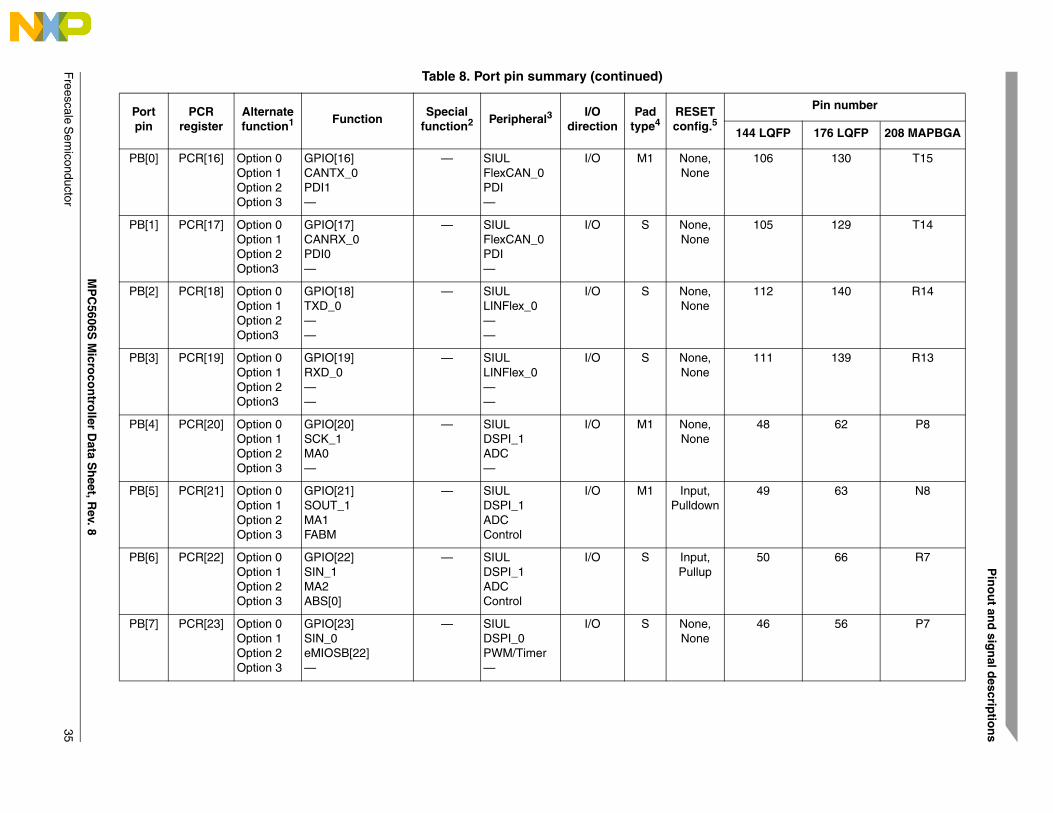
Pin
ou
t and
sign
al descrip
tion
s
MP
C5606S
Micro
con
troller D
ata Sh
eet, Rev. 8
Freescale S
emiconductor
35
PB[0] PCR[16] Option 0Option 1Option 2Option 3
GPIO[16]CANTX_0PDI1—
— SIULFlexCAN_0PDI—
I/O M1 None, None
106 130 T15
PB[1] PCR[17] Option 0Option 1Option 2Option3
GPIO[17]CANRX_0PDI0—
— SIULFlexCAN_0PDI—
I/O S None, None
105 129 T14
PB[2] PCR[18] Option 0Option 1Option 2Option3
GPIO[18]TXD_0——
— SIULLINFlex_0——
I/O S None, None
112 140 R14
PB[3] PCR[19] Option 0Option 1Option 2Option3
GPIO[19]RXD_0——
— SIULLINFlex_0——
I/O S None, None
111 139 R13
PB[4] PCR[20] Option 0Option 1Option 2Option 3
GPIO[20]SCK_1MA0—
— SIULDSPI_1ADC—
I/O M1 None, None
48 62 P8
PB[5] PCR[21] Option 0Option 1Option 2Option 3
GPIO[21]SOUT_1MA1FABM
— SIULDSPI_1ADCControl
I/O M1 Input, Pulldown
49 63 N8
PB[6] PCR[22] Option 0Option 1Option 2Option 3
GPIO[22]SIN_1MA2ABS[0]
— SIULDSPI_1ADCControl
I/O S Input, Pullup
50 66 R7
PB[7] PCR[23] Option 0Option 1Option 2Option 3
GPIO[23]SIN_0eMIOSB[22]—
— SIULDSPI_0PWM/Timer—
I/O S None, None
46 56 P7
Table 8. Port pin summary (continued)
Portpin
PCRregister
Alternatefunction1 Function
Specialfunction2 Peripheral3
I/Odirection
Padtype4
RESETconfig.5
Pin number
144 LQFP 176 LQFP 208 MAPBGA
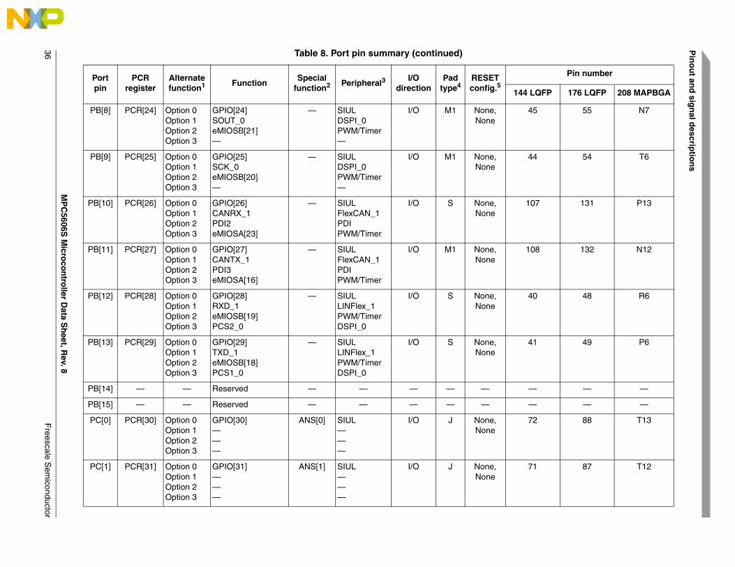
MP
C5606S
Micro
con
troller D
ata Sh
eet, Rev. 8
Pin
ou
t and
sign
al descrip
tion
s
Freescale S
emiconductor
36
PB[8] PCR[24] Option 0Option 1Option 2Option 3
GPIO[24]SOUT_0eMIOSB[21]—
— SIULDSPI_0PWM/Timer—
I/O M1 None, None
45 55 N7
PB[9] PCR[25] Option 0Option 1Option 2Option 3
GPIO[25]SCK_0eMIOSB[20]—
— SIULDSPI_0PWM/Timer—
I/O M1 None, None
44 54 T6
PB[10] PCR[26] Option 0Option 1Option 2Option 3
GPIO[26]CANRX_1PDI2eMIOSA[23]
— SIULFlexCAN_1PDIPWM/Timer
I/O S None, None
107 131 P13
PB[11] PCR[27] Option 0Option 1Option 2Option 3
GPIO[27]CANTX_1PDI3eMIOSA[16]
— SIULFlexCAN_1PDIPWM/Timer
I/O M1 None, None
108 132 N12
PB[12] PCR[28] Option 0Option 1Option 2Option 3
GPIO[28]RXD_1eMIOSB[19]PCS2_0
— SIULLINFlex_1PWM/TimerDSPI_0
I/O S None, None
40 48 R6
PB[13] PCR[29] Option 0Option 1Option 2Option 3
GPIO[29]TXD_1eMIOSB[18]PCS1_0
— SIULLINFlex_1PWM/TimerDSPI_0
I/O S None, None
41 49 P6
PB[14] — — Reserved — — — — — — — —
PB[15] — — Reserved — — — — — — — —
PC[0] PCR[30] Option 0Option 1Option 2Option 3
GPIO[30]———
ANS[0] SIUL———
I/O J None, None
72 88 T13
PC[1] PCR[31] Option 0Option 1Option 2Option 3
GPIO[31]———
ANS[1] SIUL———
I/O J None, None
71 87 T12
Table 8. Port pin summary (continued)
Portpin
PCRregister
Alternatefunction1 Function
Specialfunction2 Peripheral3
I/Odirection
Padtype4
RESETconfig.5
Pin number
144 LQFP 176 LQFP 208 MAPBGA

Pin
ou
t and
sign
al descrip
tion
s
MP
C5606S
Micro
con
troller D
ata Sh
eet, Rev. 8
Freescale S
emiconductor
37
PC[2] PCR[32] Option 0Option 1Option 2Option 3
GPIO[32]———
ANS[2] SIUL———
I/O J None, None
70 86 R12
PC[3] PCR[33] Option 0Option 1Option 2Option 3
GPIO[33]———
ANS[3] SIUL———
I/O J None, None
69 85 P12
PC[4] PCR[34] Option 0Option 1Option 2Option 3
GPIO[34]———
ANS[4] SIUL———
I/O J None, None
68 84 R11
PC[5] PCR[35] Option 0Option 1Option 2Option 3
GPIO[35]———
ANS[5] SIUL———
I/O J None, None
67 83 P11
PC[6] PCR[36] Option 0Option 1Option 2Option 3
GPIO[36]———
ANS[6] SIUL———
I/O J None, None
66 82 N11
PC[7] PCR[37] Option 0Option 1Option 2Option 3
GPIO[37]———
ANS[7] SIUL———
I/O J None, None
65 81 R10
PC[8] PCR[38] Option 0Option 1Option 2Option 3
GPIO[38]———
ANS[8] SIUL———
I/O J None, None
62 78 P10
PC[9] PCR[39] Option 0Option 1Option 2Option 3
GPIO[39]———
ANS[9] SIUL———
I/O J None, None
61 77 N10
Table 8. Port pin summary (continued)
Portpin
PCRregister
Alternatefunction1 Function
Specialfunction2 Peripheral3
I/Odirection
Padtype4
RESETconfig.5
Pin number
144 LQFP 176 LQFP 208 MAPBGA
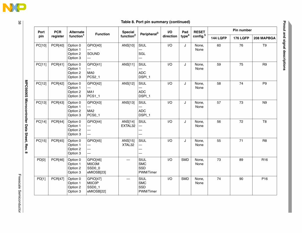
MP
C5606S
Micro
con
troller D
ata Sh
eet, Rev. 8
Pin
ou
t and
sign
al descrip
tion
s
Freescale S
emiconductor
38
PC[10] PCR[40] Option 0Option 1Option 2Option 3
GPIO[40]—SOUND—
ANS[10] SIUL—SGL—
I/O J None, None
60 76 T9
PC[11] PCR[41] Option 0Option 1Option 2Option 3
GPIO[41]—MA0PCS2_1
ANS[11] SIUL—ADCDSPI_1
I/O J None, None
59 75 R9
PC[12] PCR[42] Option 0Option 1Option 2Option 3
GPIO[42]—MA1PCS1_1
ANS[12] SIUL—ADCDSPI_1
I/O J None, None
58 74 P9
PC[13] PCR[43] Option 0Option 1Option 2Option 3
GPIO[43]—MA2PCS0_1
ANS[13] SIUL—ADCDSPI_1
I/O J None, None
57 73 N9
PC[14] PCR[44] Option 0Option 1Option 2Option 3
GPIO[44]———
ANS[14]EXTAL32
SIUL———
I/O J None, None
56 72 T8
PC[15] PCR[45] Option 0Option 1Option 2Option 3
GPIO[45]———
ANS[15]XTAL32
SIUL———
I/O J None, None
55 71 R8
PD[0] PCR[46] Option 0Option 1Option 2Option 3
GPIO[46]M0C0MSSD0_0eMIOSB[23]
— SIULSMCSSDPWM/Timer
I/O SMD None, None
73 89 R16
PD[1] PCR[47] Option 0Option 1Option 2Option 3
GPIO[47]M0C0PSSD0_1eMIOSB[22]
— SIULSMCSSDPWM/Timer
I/O SMD None, None
74 90 P16
Table 8. Port pin summary (continued)
Portpin
PCRregister
Alternatefunction1 Function
Specialfunction2 Peripheral3
I/Odirection
Padtype4
RESETconfig.5
Pin number
144 LQFP 176 LQFP 208 MAPBGA
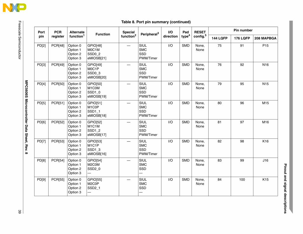
Pin
ou
t and
sign
al descrip
tion
s
MP
C5606S
Micro
con
troller D
ata Sh
eet, Rev. 8
Freescale S
emiconductor
39
PD[2] PCR[48] Option 0Option 1Option 2Option 3
GPIO[48]M0C1MSSD0_2eMIOSB[21]
— SIULSMCSSDPWM/Timer
I/O SMD None, None
75 91 P15
PD[3] PCR[49] Option 0Option 1Option 2Option 3
GPIO[49]M0C1PSSD0_3eMIOSB[20]
— SIULSMCSSDPWM/Timer
I/O SMD None, None
76 92 N16
PD[4] PCR[50] Option 0Option 1Option 2Option 3
GPIO[50]M1C0MSSD1_0eMIOSB[19]
— SIULSMCSSDPWM/Timer
I/O SMD None, None
79 95 N15
PD[5] PCR[51] Option 0Option 1Option 2Option 3
GPIO[51]M1C0PSSD1_1eMIOSB[18]
— SIULSMCSSDPWM/Timer
I/O SMD None, None
80 96 M15
PD[6] PCR[52] Option 0Option 1Option 2Option 3
GPIO[52]M1C1MSSD1_2eMIOSB[17]
— SIULSMCSSDPWM/Timer
I/O SMD None, None
81 97 M16
PD[7] PCR[53] Option 0Option 1Option 2Option 3
GPIO[53]M1C1PSSD1_3eMIOSB[16]
— SIULSMCSSDPWM/Timer
I/O SMD None, None
82 98 K16
PD[8] PCR[54] Option 0Option 1Option 2Option 3
GPIO[54]M2C0MSSD2_0—
— SIULSMCSSD—
I/O SMD None, None
83 99 J16
PD[9] PCR[55] Option 0Option 1Option 2Option 3
GPIO[55]M2C0PSSD2_1—
— SIULSMCSSD—
I/O SMD None, None
84 100 K15
Table 8. Port pin summary (continued)
Portpin
PCRregister
Alternatefunction1 Function
Specialfunction2 Peripheral3
I/Odirection
Padtype4
RESETconfig.5
Pin number
144 LQFP 176 LQFP 208 MAPBGA
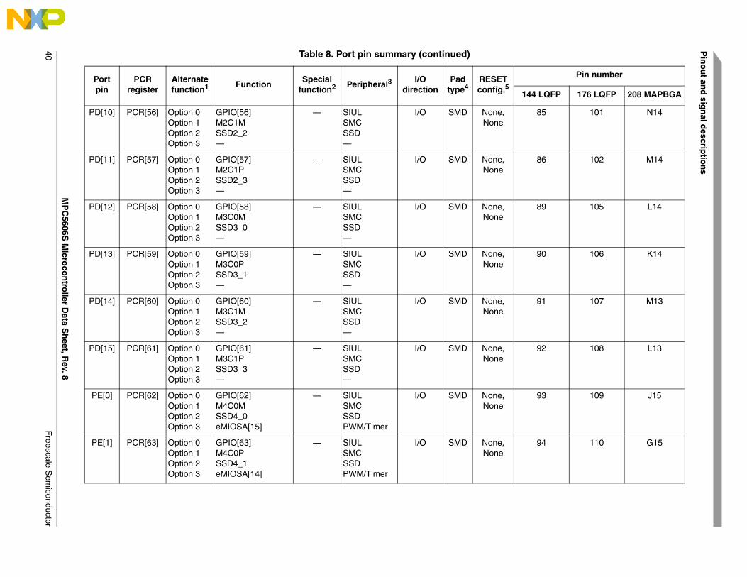
MP
C5606S
Micro
con
troller D
ata Sh
eet, Rev. 8
Pin
ou
t and
sign
al descrip
tion
s
Freescale S
emiconductor
40
PD[10] PCR[56] Option 0Option 1Option 2Option 3
GPIO[56]M2C1MSSD2_2—
— SIULSMCSSD—
I/O SMD None, None
85 101 N14
PD[11] PCR[57] Option 0Option 1Option 2Option 3
GPIO[57]M2C1PSSD2_3—
— SIULSMCSSD—
I/O SMD None, None
86 102 M14
PD[12] PCR[58] Option 0Option 1Option 2Option 3
GPIO[58]M3C0MSSD3_0—
— SIULSMCSSD—
I/O SMD None, None
89 105 L14
PD[13] PCR[59] Option 0Option 1Option 2Option 3
GPIO[59]M3C0PSSD3_1—
— SIULSMCSSD—
I/O SMD None, None
90 106 K14
PD[14] PCR[60] Option 0Option 1Option 2Option 3
GPIO[60]M3C1MSSD3_2—
— SIULSMCSSD—
I/O SMD None, None
91 107 M13
PD[15] PCR[61] Option 0Option 1Option 2Option 3
GPIO[61]M3C1PSSD3_3—
— SIULSMCSSD—
I/O SMD None, None
92 108 L13
PE[0] PCR[62] Option 0Option 1Option 2Option 3
GPIO[62]M4C0MSSD4_0eMIOSA[15]
— SIULSMCSSDPWM/Timer
I/O SMD None, None
93 109 J15
PE[1] PCR[63] Option 0Option 1Option 2Option 3
GPIO[63]M4C0PSSD4_1eMIOSA[14]
— SIULSMCSSDPWM/Timer
I/O SMD None, None
94 110 G15
Table 8. Port pin summary (continued)
Portpin
PCRregister
Alternatefunction1 Function
Specialfunction2 Peripheral3
I/Odirection
Padtype4
RESETconfig.5
Pin number
144 LQFP 176 LQFP 208 MAPBGA
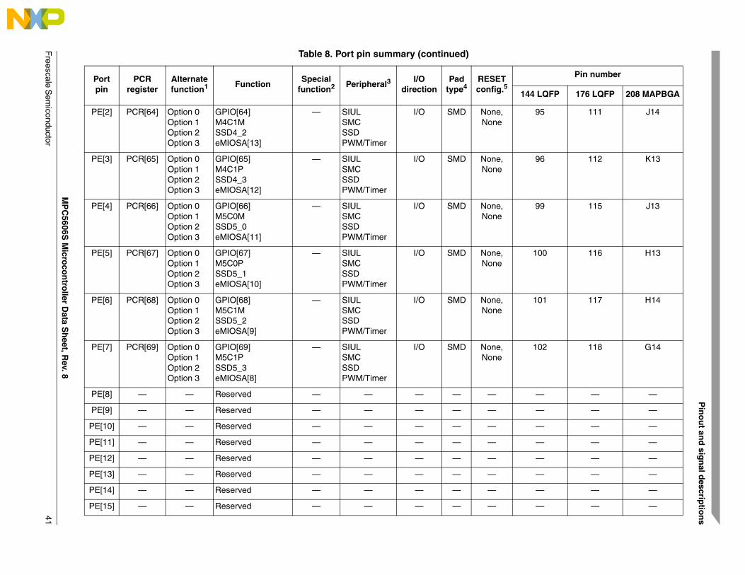
Pin
ou
t and
sign
al descrip
tion
s
MP
C5606S
Micro
con
troller D
ata Sh
eet, Rev. 8
Freescale S
emiconductor
41
PE[2] PCR[64] Option 0Option 1Option 2Option 3
GPIO[64]M4C1MSSD4_2eMIOSA[13]
— SIULSMCSSDPWM/Timer
I/O SMD None, None
95 111 J14
PE[3] PCR[65] Option 0Option 1Option 2Option 3
GPIO[65]M4C1PSSD4_3eMIOSA[12]
— SIULSMCSSDPWM/Timer
I/O SMD None, None
96 112 K13
PE[4] PCR[66] Option 0Option 1Option 2Option 3
GPIO[66]M5C0MSSD5_0eMIOSA[11]
— SIULSMCSSDPWM/Timer
I/O SMD None, None
99 115 J13
PE[5] PCR[67] Option 0Option 1Option 2Option 3
GPIO[67]M5C0PSSD5_1eMIOSA[10]
— SIULSMCSSDPWM/Timer
I/O SMD None, None
100 116 H13
PE[6] PCR[68] Option 0Option 1Option 2Option 3
GPIO[68]M5C1MSSD5_2eMIOSA[9]
— SIULSMCSSDPWM/Timer
I/O SMD None, None
101 117 H14
PE[7] PCR[69] Option 0Option 1Option 2Option 3
GPIO[69]M5C1PSSD5_3eMIOSA[8]
— SIULSMCSSDPWM/Timer
I/O SMD None, None
102 118 G14
PE[8] — — Reserved — — — — — — — —
PE[9] — — Reserved — — — — — — — —
PE[10] — — Reserved — — — — — — — —
PE[11] — — Reserved — — — — — — — —
PE[12] — — Reserved — — — — — — — —
PE[13] — — Reserved — — — — — — — —
PE[14] — — Reserved — — — — — — — —
PE[15] — — Reserved — — — — — — — —
Table 8. Port pin summary (continued)
Portpin
PCRregister
Alternatefunction1 Function
Specialfunction2 Peripheral3
I/Odirection
Padtype4
RESETconfig.5
Pin number
144 LQFP 176 LQFP 208 MAPBGA
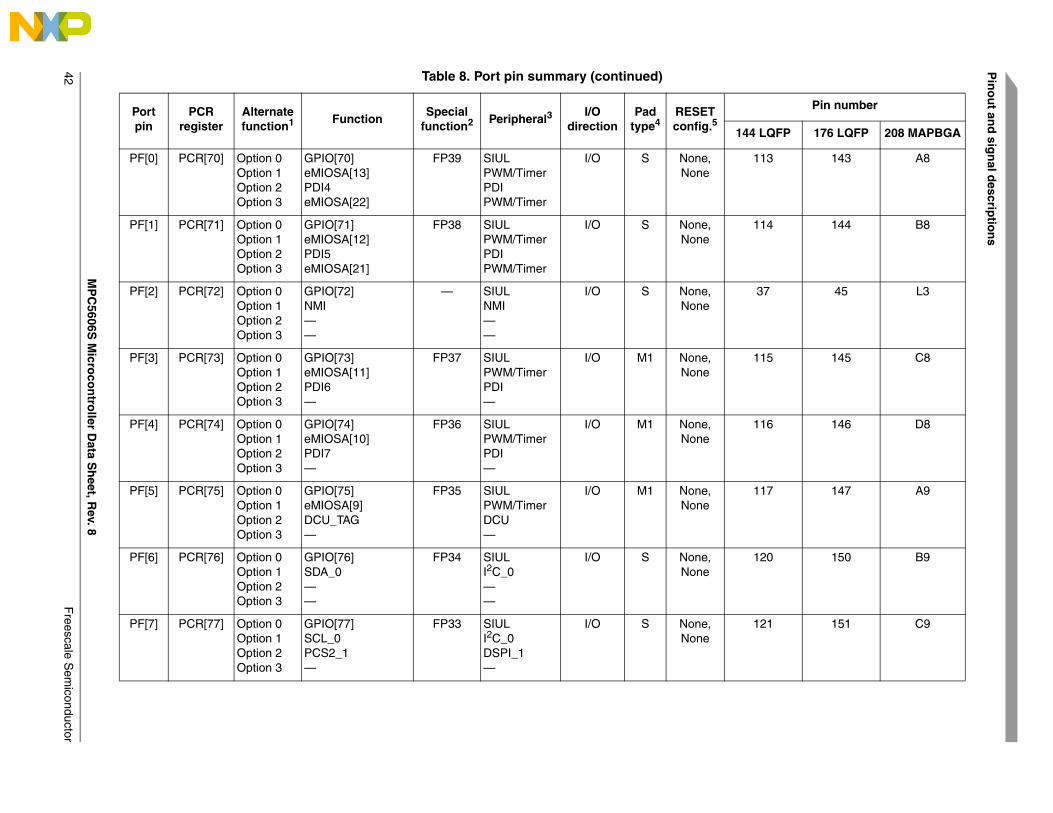
MP
C5606S
Micro
con
troller D
ata Sh
eet, Rev. 8
Pin
ou
t and
sign
al descrip
tion
s
Freescale S
emiconductor
42
PF[0] PCR[70] Option 0Option 1Option 2Option 3
GPIO[70]eMIOSA[13]PDI4eMIOSA[22]
FP39 SIULPWM/TimerPDIPWM/Timer
I/O S None, None
113 143 A8
PF[1] PCR[71] Option 0Option 1Option 2Option 3
GPIO[71]eMIOSA[12]PDI5eMIOSA[21]
FP38 SIULPWM/TimerPDIPWM/Timer
I/O S None, None
114 144 B8
PF[2] PCR[72] Option 0Option 1Option 2Option 3
GPIO[72]NMI——
— SIULNMI——
I/O S None, None
37 45 L3
PF[3] PCR[73] Option 0Option 1Option 2Option 3
GPIO[73]eMIOSA[11]PDI6—
FP37 SIULPWM/TimerPDI—
I/O M1 None, None
115 145 C8
PF[4] PCR[74] Option 0Option 1Option 2Option 3
GPIO[74]eMIOSA[10]PDI7—
FP36 SIULPWM/TimerPDI—
I/O M1 None, None
116 146 D8
PF[5] PCR[75] Option 0Option 1Option 2Option 3
GPIO[75]eMIOSA[9]DCU_TAG—
FP35 SIULPWM/TimerDCU—
I/O M1 None, None
117 147 A9
PF[6] PCR[76] Option 0Option 1Option 2Option 3
GPIO[76]SDA_0——
FP34 SIULI2C_0——
I/O S None, None
120 150 B9
PF[7] PCR[77] Option 0Option 1Option 2Option 3
GPIO[77]SCL_0PCS2_1—
FP33 SIULI2C_0DSPI_1—
I/O S None, None
121 151 C9
Table 8. Port pin summary (continued)
Portpin
PCRregister
Alternatefunction1 Function
Specialfunction2 Peripheral3
I/Odirection
Padtype4
RESETconfig.5
Pin number
144 LQFP 176 LQFP 208 MAPBGA
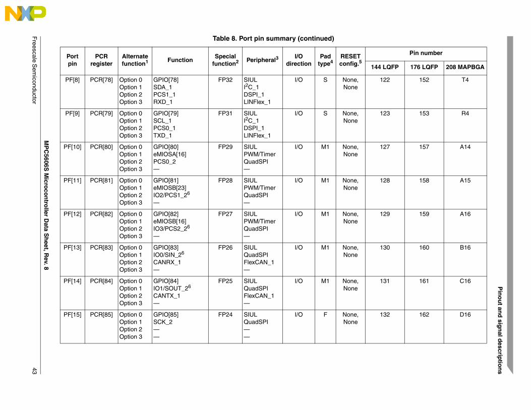
Pin
ou
t and
sign
al descrip
tion
s
MP
C5606S
Micro
con
troller D
ata Sh
eet, Rev. 8
Freescale S
emiconductor
43
PF[8] PCR[78] Option 0Option 1Option 2Option 3
GPIO[78]SDA_1PCS1_1RXD_1
FP32 SIULI2C_1DSPI_1LINFlex_1
I/O S None, None
122 152 T4
PF[9] PCR[79] Option 0Option 1Option 2Option 3
GPIO[79]SCL_1PCS0_1TXD_1
FP31 SIULI2C_1DSPI_1LINFlex_1
I/O S None, None
123 153 R4
PF[10] PCR[80] Option 0Option 1Option 2Option 3
GPIO[80]eMIOSA[16]PCS0_2—
FP29 SIULPWM/TimerQuadSPI—
I/O M1 None, None
127 157 A14
PF[11] PCR[81] Option 0Option 1Option 2Option 3
GPIO[81]eMIOSB[23]IO2/PCS1_26
—
FP28 SIULPWM/TimerQuadSPI—
I/O M1 None, None
128 158 A15
PF[12] PCR[82] Option 0Option 1Option 2Option 3
GPIO[82]eMIOSB[16]IO3/PCS2_26
—
FP27 SIULPWM/TimerQuadSPI—
I/O M1 None, None
129 159 A16
PF[13] PCR[83] Option 0Option 1Option 2Option 3
GPIO[83]IO0/SIN_26
CANRX_1—
FP26 SIULQuadSPIFlexCAN_1—
I/O M1 None, None
130 160 B16
PF[14] PCR[84] Option 0Option 1Option 2Option 3
GPIO[84]IO1/SOUT_26
CANTX_1—
FP25 SIULQuadSPIFlexCAN_1—
I/O M1 None, None
131 161 C16
PF[15] PCR[85] Option 0Option 1Option 2Option 3
GPIO[85]SCK_2——
FP24 SIULQuadSPI——
I/O F None, None
132 162 D16
Table 8. Port pin summary (continued)
Portpin
PCRregister
Alternatefunction1 Function
Specialfunction2 Peripheral3
I/Odirection
Padtype4
RESETconfig.5
Pin number
144 LQFP 176 LQFP 208 MAPBGA
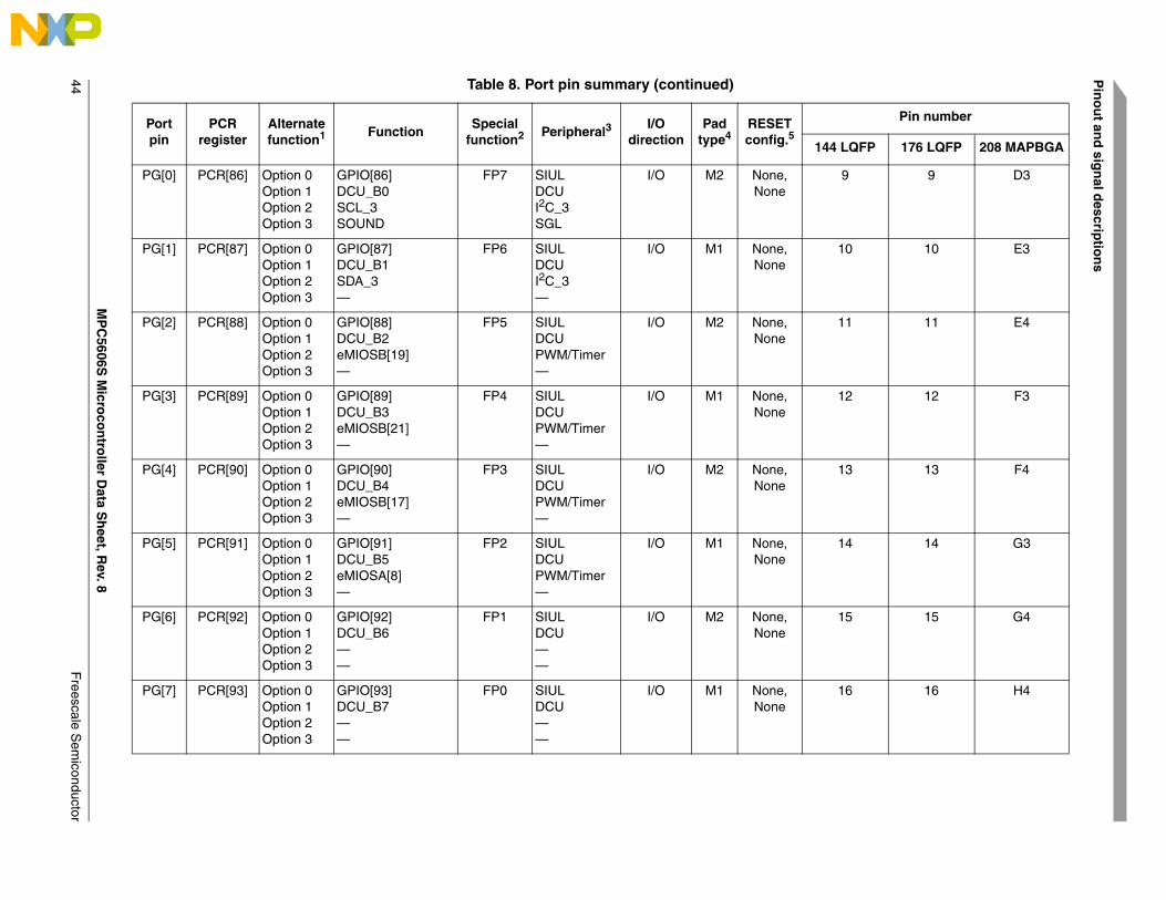
MP
C5606S
Micro
con
troller D
ata Sh
eet, Rev. 8
Pin
ou
t and
sign
al descrip
tion
s
Freescale S
emiconductor
44
PG[0] PCR[86] Option 0Option 1Option 2Option 3
GPIO[86]DCU_B0SCL_3SOUND
FP7 SIULDCUI2C_3SGL
I/O M2 None, None
9 9 D3
PG[1] PCR[87] Option 0Option 1Option 2Option 3
GPIO[87]DCU_B1SDA_3—
FP6 SIULDCUI2C_3—
I/O M1 None, None
10 10 E3
PG[2] PCR[88] Option 0Option 1Option 2Option 3
GPIO[88]DCU_B2eMIOSB[19]—
FP5 SIULDCUPWM/Timer—
I/O M2 None, None
11 11 E4
PG[3] PCR[89] Option 0Option 1Option 2Option 3
GPIO[89]DCU_B3eMIOSB[21]—
FP4 SIULDCUPWM/Timer—
I/O M1 None, None
12 12 F3
PG[4] PCR[90] Option 0Option 1Option 2Option 3
GPIO[90]DCU_B4eMIOSB[17]—
FP3 SIULDCUPWM/Timer—
I/O M2 None, None
13 13 F4
PG[5] PCR[91] Option 0Option 1Option 2Option 3
GPIO[91]DCU_B5eMIOSA[8]—
FP2 SIULDCUPWM/Timer—
I/O M1 None, None
14 14 G3
PG[6] PCR[92] Option 0Option 1Option 2Option 3
GPIO[92]DCU_B6——
FP1 SIULDCU——
I/O M2 None, None
15 15 G4
PG[7] PCR[93] Option 0Option 1Option 2Option 3
GPIO[93]DCU_B7——
FP0 SIULDCU——
I/O M1 None, None
16 16 H4
Table 8. Port pin summary (continued)
Portpin
PCRregister
Alternatefunction1 Function
Specialfunction2 Peripheral3
I/Odirection
Padtype4
RESETconfig.5
Pin number
144 LQFP 176 LQFP 208 MAPBGA
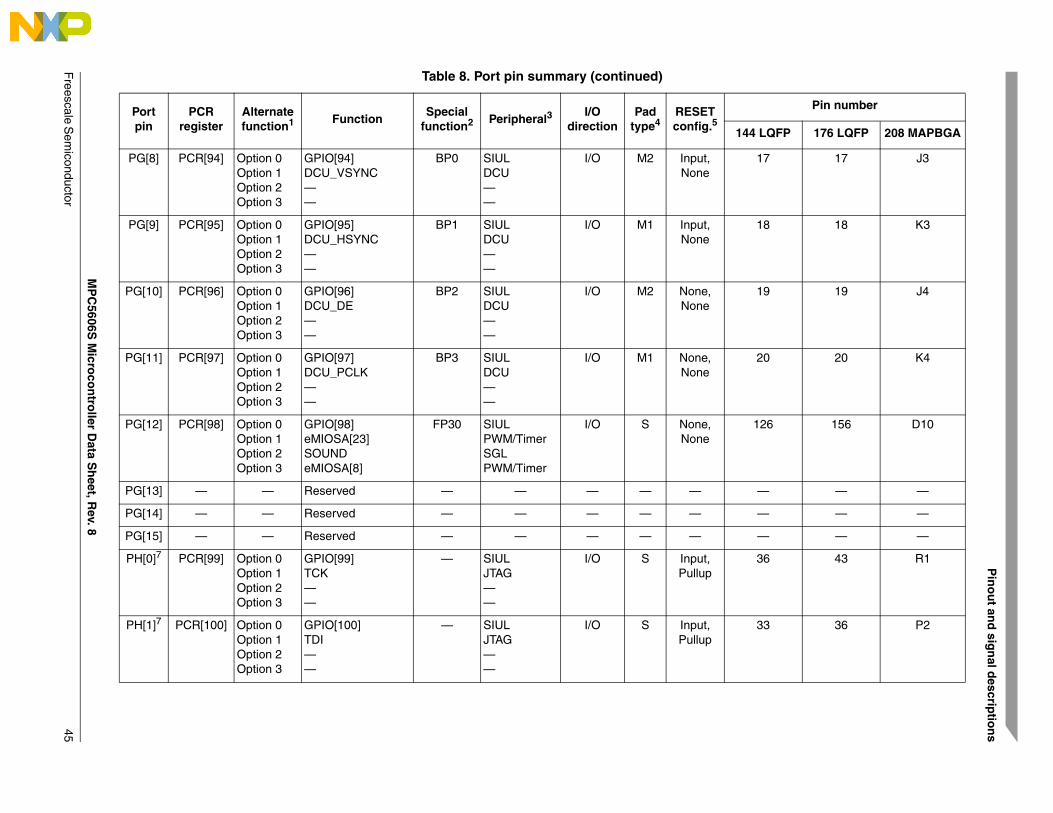
Pin
ou
t and
sign
al descrip
tion
s
MP
C5606S
Micro
con
troller D
ata Sh
eet, Rev. 8
Freescale S
emiconductor
45
PG[8] PCR[94] Option 0Option 1Option 2Option 3
GPIO[94]DCU_VSYNC——
BP0 SIULDCU——
I/O M2 Input, None
17 17 J3
PG[9] PCR[95] Option 0Option 1Option 2Option 3
GPIO[95]DCU_HSYNC——
BP1 SIULDCU——
I/O M1 Input, None
18 18 K3
PG[10] PCR[96] Option 0Option 1Option 2Option 3
GPIO[96]DCU_DE——
BP2 SIULDCU——
I/O M2 None, None
19 19 J4
PG[11] PCR[97] Option 0Option 1Option 2Option 3
GPIO[97]DCU_PCLK——
BP3 SIULDCU——
I/O M1 None, None
20 20 K4
PG[12] PCR[98] Option 0Option 1Option 2Option 3
GPIO[98]eMIOSA[23]SOUNDeMIOSA[8]
FP30 SIULPWM/TimerSGLPWM/Timer
I/O S None, None
126 156 D10
PG[13] — — Reserved — — — — — — — —
PG[14] — — Reserved — — — — — — — —
PG[15] — — Reserved — — — — — — — —
PH[0]7 PCR[99] Option 0Option 1Option 2Option 3
GPIO[99]TCK——
— SIULJTAG——
I/O S Input, Pullup
36 43 R1
PH[1]7 PCR[100] Option 0Option 1Option 2Option 3
GPIO[100]TDI——
— SIULJTAG——
I/O S Input, Pullup
33 36 P2
Table 8. Port pin summary (continued)
Portpin
PCRregister
Alternatefunction1 Function
Specialfunction2 Peripheral3
I/Odirection
Padtype4
RESETconfig.5
Pin number
144 LQFP 176 LQFP 208 MAPBGA
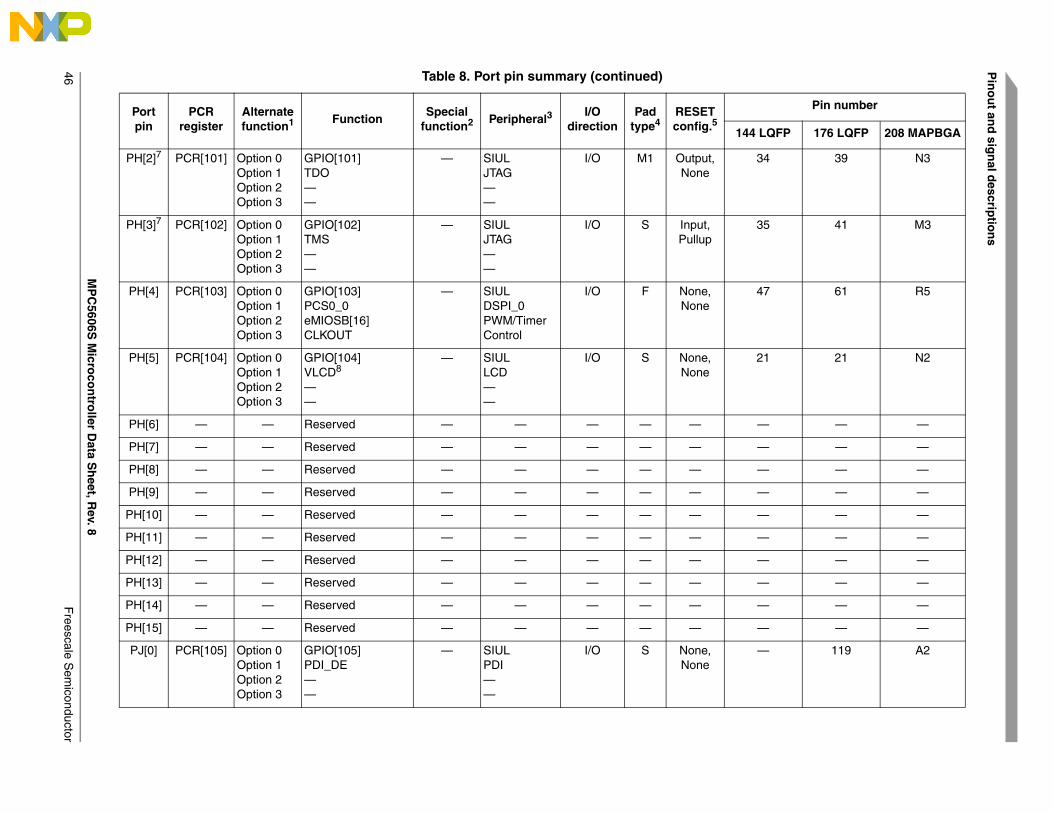
MP
C5606S
Micro
con
troller D
ata Sh
eet, Rev. 8
Pin
ou
t and
sign
al descrip
tion
s
Freescale S
emiconductor
46
PH[2]7 PCR[101] Option 0Option 1Option 2Option 3
GPIO[101]TDO——
— SIULJTAG——
I/O M1 Output, None
34 39 N3
PH[3]7 PCR[102] Option 0Option 1Option 2Option 3
GPIO[102]TMS——
— SIULJTAG——
I/O S Input, Pullup
35 41 M3
PH[4] PCR[103] Option 0Option 1Option 2Option 3
GPIO[103]PCS0_0eMIOSB[16]CLKOUT
— SIULDSPI_0PWM/TimerControl
I/O F None, None
47 61 R5
PH[5] PCR[104] Option 0Option 1Option 2Option 3
GPIO[104]VLCD8
——
— SIULLCD——
I/O S None, None
21 21 N2
PH[6] — — Reserved — — — — — — — —
PH[7] — — Reserved — — — — — — — —
PH[8] — — Reserved — — — — — — — —
PH[9] — — Reserved — — — — — — — —
PH[10] — — Reserved — — — — — — — —
PH[11] — — Reserved — — — — — — — —
PH[12] — — Reserved — — — — — — — —
PH[13] — — Reserved — — — — — — — —
PH[14] — — Reserved — — — — — — — —
PH[15] — — Reserved — — — — — — — —
PJ[0] PCR[105] Option 0Option 1Option 2Option 3
GPIO[105]PDI_DE——
— SIULPDI——
I/O S None, None
— 119 A2
Table 8. Port pin summary (continued)
Portpin
PCRregister
Alternatefunction1 Function
Specialfunction2 Peripheral3
I/Odirection
Padtype4
RESETconfig.5
Pin number
144 LQFP 176 LQFP 208 MAPBGA
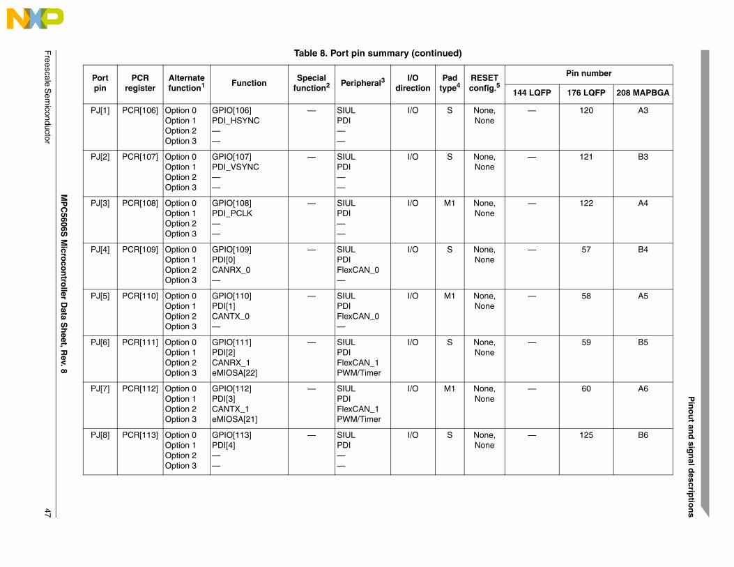
Pin
ou
t and
sign
al descrip
tion
s
MP
C5606S
Micro
con
troller D
ata Sh
eet, Rev. 8
Freescale S
emiconductor
47
PJ[1] PCR[106] Option 0Option 1Option 2Option 3
GPIO[106]PDI_HSYNC——
— SIULPDI——
I/O S None, None
— 120 A3
PJ[2] PCR[107] Option 0Option 1Option 2Option 3
GPIO[107]PDI_VSYNC——
— SIULPDI——
I/O S None, None
— 121 B3
PJ[3] PCR[108] Option 0Option 1Option 2Option 3
GPIO[108]PDI_PCLK——
— SIULPDI——
I/O M1 None, None
— 122 A4
PJ[4] PCR[109] Option 0Option 1Option 2Option 3
GPIO[109]PDI[0]CANRX_0—
— SIULPDIFlexCAN_0—
I/O S None, None
— 57 B4
PJ[5] PCR[110] Option 0Option 1Option 2Option 3
GPIO[110]PDI[1]CANTX_0—
— SIULPDIFlexCAN_0—
I/O M1 None, None
— 58 A5
PJ[6] PCR[111] Option 0Option 1Option 2Option 3
GPIO[111]PDI[2]CANRX_1eMIOSA[22]
— SIULPDIFlexCAN_1PWM/Timer
I/O S None, None
— 59 B5
PJ[7] PCR[112] Option 0Option 1Option 2Option 3
GPIO[112]PDI[3]CANTX_1eMIOSA[21]
— SIULPDIFlexCAN_1PWM/Timer
I/O M1 None, None
— 60 A6
PJ[8] PCR[113] Option 0Option 1Option 2Option 3
GPIO[113]PDI[4]——
— SIULPDI——
I/O S None, None
— 125 B6
Table 8. Port pin summary (continued)
Portpin
PCRregister
Alternatefunction1 Function
Specialfunction2 Peripheral3
I/Odirection
Padtype4
RESETconfig.5
Pin number
144 LQFP 176 LQFP 208 MAPBGA
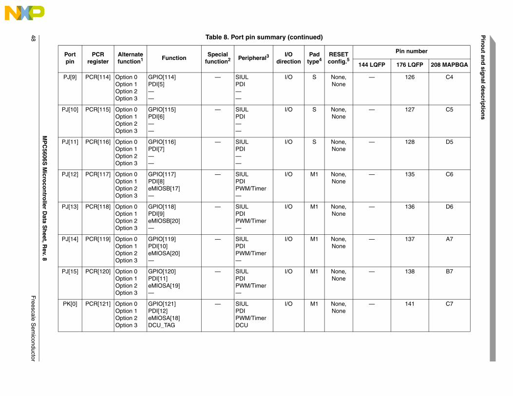
MP
C5606S
Micro
con
troller D
ata Sh
eet, Rev. 8
Pin
ou
t and
sign
al descrip
tion
s
Freescale S
emiconductor
48
PJ[9] PCR[114] Option 0Option 1Option 2Option 3
GPIO[114]PDI[5]——
— SIULPDI——
I/O S None, None
— 126 C4
PJ[10] PCR[115] Option 0Option 1Option 2Option 3
GPIO[115]PDI[6]——
— SIULPDI——
I/O S None, None
— 127 C5
PJ[11] PCR[116] Option 0Option 1Option 2Option 3
GPIO[116]PDI[7]——
— SIULPDI——
I/O S None, None
— 128 D5
PJ[12] PCR[117] Option 0Option 1Option 2Option 3
GPIO[117]PDI[8]eMIOSB[17]—
— SIULPDIPWM/Timer—
I/O M1 None, None
— 135 C6
PJ[13] PCR[118] Option 0Option 1Option 2Option 3
GPIO[118]PDI[9]eMIOSB[20]—
— SIULPDIPWM/Timer—
I/O M1 None, None
— 136 D6
PJ[14] PCR[119] Option 0Option 1Option 2Option 3
GPIO[119]PDI[10]eMIOSA[20]—
— SIULPDIPWM/Timer—
I/O M1 None, None
— 137 A7
PJ[15] PCR[120] Option 0Option 1Option 2Option 3
GPIO[120]PDI[11]eMIOSA[19]—
— SIULPDIPWM/Timer—
I/O M1 None, None
— 138 B7
PK[0] PCR[121] Option 0Option 1Option 2Option 3
GPIO[121]PDI[12]eMIOSA[18]DCU_TAG
— SIULPDIPWM/TimerDCU
I/O M1 None, None
— 141 C7
Table 8. Port pin summary (continued)
Portpin
PCRregister
Alternatefunction1 Function
Specialfunction2 Peripheral3
I/Odirection
Padtype4
RESETconfig.5
Pin number
144 LQFP 176 LQFP 208 MAPBGA
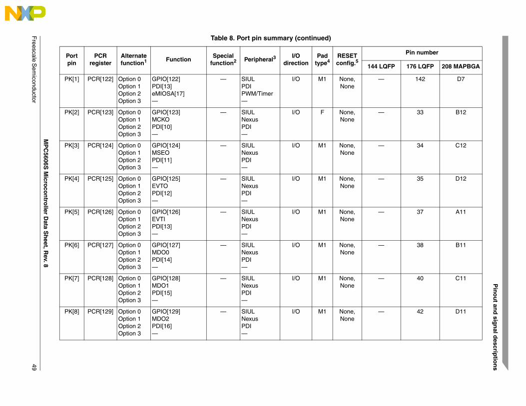
Pin
ou
t and
sign
al descrip
tion
s
MP
C5606S
Micro
con
troller D
ata Sh
eet, Rev. 8
Freescale S
emiconductor
49
PK[1] PCR[122] Option 0Option 1Option 2Option 3
GPIO[122]PDI[13]eMIOSA[17]—
— SIULPDIPWM/Timer—
I/O M1 None, None
— 142 D7
PK[2] PCR[123] Option 0Option 1Option 2Option 3
GPIO[123]MCKOPDI[10]—
— SIULNexusPDI—
I/O F None, None
— 33 B12
PK[3] PCR[124] Option 0Option 1Option 2Option 3
GPIO[124]MSEOPDI[11]—
— SIULNexusPDI—
I/O M1 None, None
— 34 C12
PK[4] PCR[125] Option 0Option 1Option 2Option 3
GPIO[125]EVTOPDI[12]—
— SIULNexusPDI—
I/O M1 None, None
— 35 D12
PK[5] PCR[126] Option 0Option 1Option 2Option 3
GPIO[126]EVTIPDI[13]—
— SIULNexusPDI—
I/O M1 None, None
— 37 A11
PK[6] PCR[127] Option 0Option 1Option 2Option 3
GPIO[127]MDO0PDI[14]—
— SIULNexusPDI—
I/O M1 None, None
— 38 B11
PK[7] PCR[128] Option 0Option 1Option 2Option 3
GPIO[128]MDO1PDI[15]—
— SIULNexusPDI—
I/O M1 None, None
— 40 C11
PK[8] PCR[129] Option 0Option 1Option 2Option 3
GPIO[129]MDO2PDI[16]—
— SIULNexusPDI—
I/O M1 None, None
— 42 D11
Table 8. Port pin summary (continued)
Portpin
PCRregister
Alternatefunction1 Function
Specialfunction2 Peripheral3
I/Odirection
Padtype4
RESETconfig.5
Pin number
144 LQFP 176 LQFP 208 MAPBGA
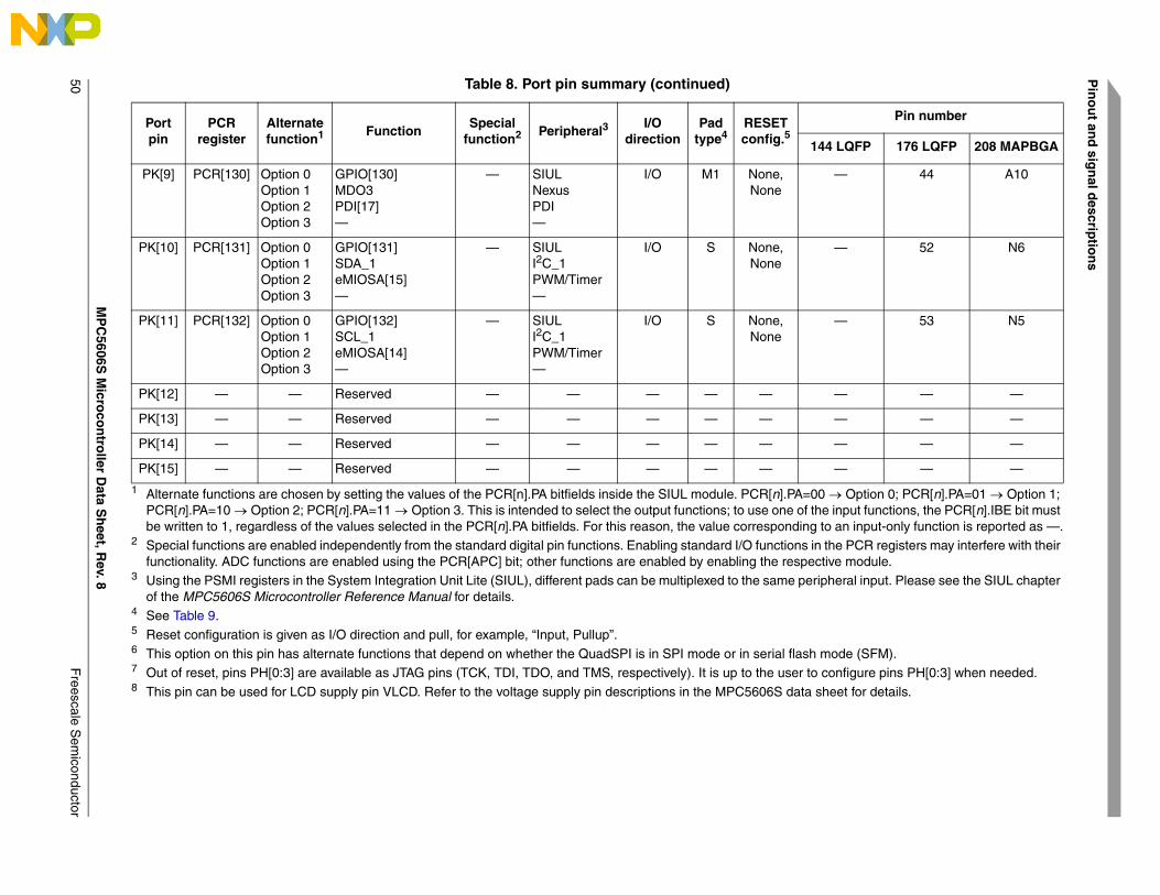
MP
C5606S
Micro
con
troller D
ata Sh
eet, Rev. 8
Pin
ou
t and
sign
al descrip
tion
s
Freescale S
emiconductor
50
PK[9] PCR[130] Option 0Option 1Option 2Option 3
GPIO[130]MDO3PDI[17]—
— SIULNexusPDI—
I/O M1 None, None
— 44 A10
PK[10] PCR[131] Option 0Option 1Option 2Option 3
GPIO[131]SDA_1eMIOSA[15]—
— SIULI2C_1PWM/Timer—
I/O S None, None
— 52 N6
PK[11] PCR[132] Option 0Option 1Option 2Option 3
GPIO[132]SCL_1eMIOSA[14]—
— SIULI2C_1PWM/Timer—
I/O S None, None
— 53 N5
PK[12] — — Reserved — — — — — — — —
PK[13] — — Reserved — — — — — — — —
PK[14] — — Reserved — — — — — — — —
PK[15] — — Reserved — — — — — — — —
1 Alternate functions are chosen by setting the values of the PCR[n].PA bitfields inside the SIUL module. PCR[n].PA=00 Option 0; PCR[n].PA=01 Option 1; PCR[n].PA=10 Option 2; PCR[n].PA=11 Option 3. This is intended to select the output functions; to use one of the input functions, the PCR[n].IBE bit must be written to 1, regardless of the values selected in the PCR[n].PA bitfields. For this reason, the value corresponding to an input-only function is reported as —.
2 Special functions are enabled independently from the standard digital pin functions. Enabling standard I/O functions in the PCR registers may interfere with their functionality. ADC functions are enabled using the PCR[APC] bit; other functions are enabled by enabling the respective module.
3 Using the PSMI registers in the System Integration Unit Lite (SIUL), different pads can be multiplexed to the same peripheral input. Please see the SIUL chapter of the MPC5606S Microcontroller Reference Manual for details.
4 See Table 9.5 Reset configuration is given as I/O direction and pull, for example, “Input, Pullup”.6 This option on this pin has alternate functions that depend on whether the QuadSPI is in SPI mode or in serial flash mode (SFM).7 Out of reset, pins PH[0:3] are available as JTAG pins (TCK, TDI, TDO, and TMS, respectively). It is up to the user to configure pins PH[0:3] when needed.8 This pin can be used for LCD supply pin VLCD. Refer to the voltage supply pin descriptions in the MPC5606S data sheet for details.
Table 8. Port pin summary (continued)
Portpin
PCRregister
Alternatefunction1 Function
Specialfunction2 Peripheral3
I/Odirection
Padtype4
RESETconfig.5
Pin number
144 LQFP 176 LQFP 208 MAPBGA
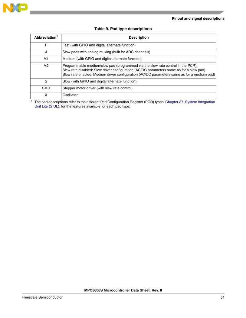
Pinout and signal descriptions
MPC5606S Microcontroller Data Sheet, Rev. 8
Freescale Semiconductor 51
Table 9. Pad type descriptions
Abbreviation1
1 The pad descriptions refer to the different Pad Configuration Register (PCR) types. Chapter 37, System Integration Unit Lite (SIUL), for the features available for each pad type.
Description
F Fast (with GPIO and digital alternate function)
J Slow pads with analog muxing (built for ADC channels)
M1 Medium (with GPIO and digital alternate function)
M2 Programmable medium/slow pad (programmed via the slew rate control in the PCR):Slew rate disabled: Slow driver configuration (AC/DC parameters same as for a slow pad)Slew rate enabled: Medium driver configuration (AC/DC parameters same as for a medium pad)
S Slow (with GPIO and digital alternate function)
SMD Stepper motor driver (with slew rate control)
X Oscillator
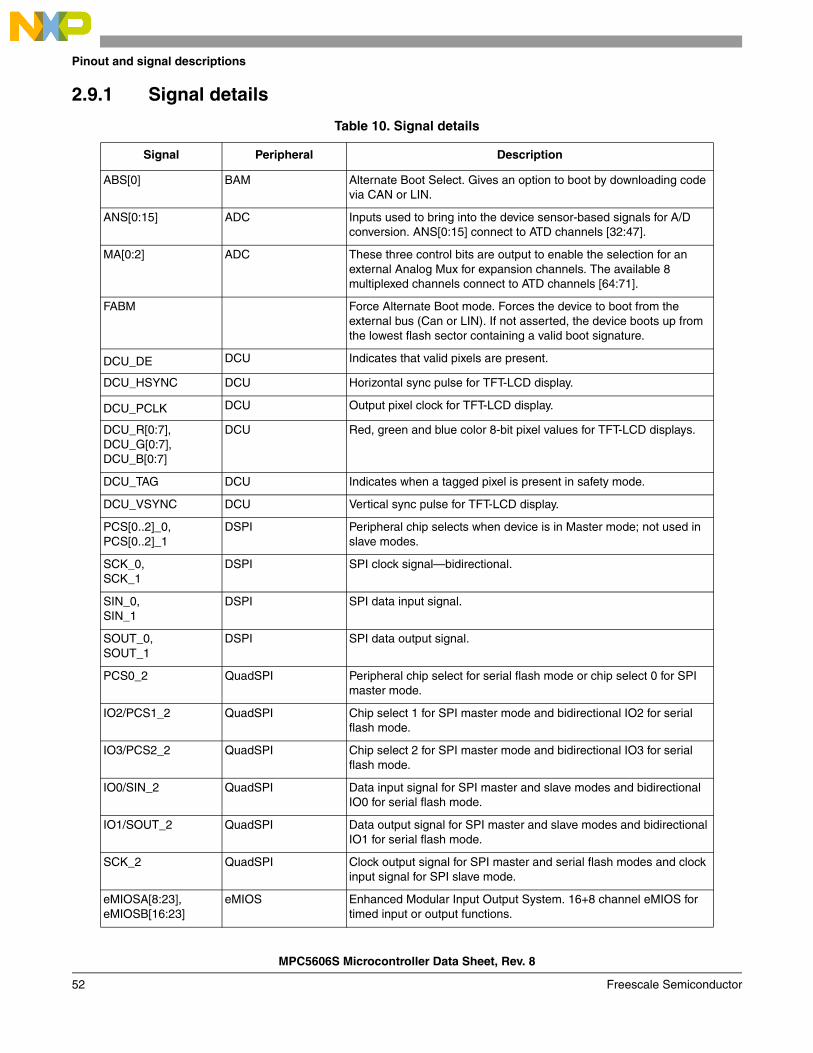
MPC5606S Microcontroller Data Sheet, Rev. 8
Pinout and signal descriptions
Freescale Semiconductor52
2.9.1 Signal details
Table 10. Signal details
Signal Peripheral Description
ABS[0] BAM Alternate Boot Select. Gives an option to boot by downloading code via CAN or LIN.
ANS[0:15] ADC Inputs used to bring into the device sensor-based signals for A/D conversion. ANS[0:15] connect to ATD channels [32:47].
MA[0:2] ADC These three control bits are output to enable the selection for an external Analog Mux for expansion channels. The available 8 multiplexed channels connect to ATD channels [64:71].
FABM Force Alternate Boot mode. Forces the device to boot from the external bus (Can or LIN). If not asserted, the device boots up from the lowest flash sector containing a valid boot signature.
DCU_DE DCU Indicates that valid pixels are present.
DCU_HSYNC DCU Horizontal sync pulse for TFT-LCD display.
DCU_PCLK DCU Output pixel clock for TFT-LCD display.
DCU_R[0:7],DCU_G[0:7],DCU_B[0:7]
DCU Red, green and blue color 8-bit pixel values for TFT-LCD displays.
DCU_TAG DCU Indicates when a tagged pixel is present in safety mode.
DCU_VSYNC DCU Vertical sync pulse for TFT-LCD display.
PCS[0..2]_0, PCS[0..2]_1
DSPI Peripheral chip selects when device is in Master mode; not used in slave modes.
SCK_0, SCK_1
DSPI SPI clock signal—bidirectional.
SIN_0, SIN_1
DSPI SPI data input signal.
SOUT_0, SOUT_1
DSPI SPI data output signal.
PCS0_2 QuadSPI Peripheral chip select for serial flash mode or chip select 0 for SPI master mode.
IO2/PCS1_2 QuadSPI Chip select 1 for SPI master mode and bidirectional IO2 for serial flash mode.
IO3/PCS2_2 QuadSPI Chip select 2 for SPI master mode and bidirectional IO3 for serial flash mode.
IO0/SIN_2 QuadSPI Data input signal for SPI master and slave modes and bidirectional IO0 for serial flash mode.
IO1/SOUT_2 QuadSPI Data output signal for SPI master and slave modes and bidirectional IO1 for serial flash mode.
SCK_2 QuadSPI Clock output signal for SPI master and serial flash modes and clock input signal for SPI slave mode.
eMIOSA[8:23],eMIOSB[16:23]
eMIOS Enhanced Modular Input Output System. 16+8 channel eMIOS for timed input or output functions.
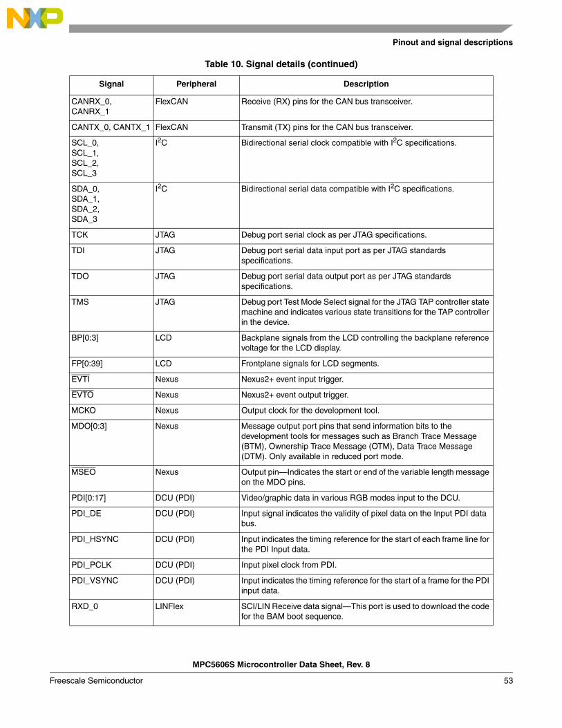
Pinout and signal descriptions
MPC5606S Microcontroller Data Sheet, Rev. 8
Freescale Semiconductor 53
CANRX_0, CANRX_1
FlexCAN Receive (RX) pins for the CAN bus transceiver.
CANTX_0, CANTX_1 FlexCAN Transmit (TX) pins for the CAN bus transceiver.
SCL_0, SCL_1, SCL_2, SCL_3
I2C Bidirectional serial clock compatible with I2C specifications.
SDA_0, SDA_1, SDA_2, SDA_3
I2C Bidirectional serial data compatible with I2C specifications.
TCK JTAG Debug port serial clock as per JTAG specifications.
TDI JTAG Debug port serial data input port as per JTAG standards specifications.
TDO JTAG Debug port serial data output port as per JTAG standards specifications.
TMS JTAG Debug port Test Mode Select signal for the JTAG TAP controller state machine and indicates various state transitions for the TAP controller in the device.
BP[0:3] LCD Backplane signals from the LCD controlling the backplane reference voltage for the LCD display.
FP[0:39] LCD Frontplane signals for LCD segments.
EVTI Nexus Nexus2+ event input trigger.
EVTO Nexus Nexus2+ event output trigger.
MCKO Nexus Output clock for the development tool.
MDO[0:3] Nexus Message output port pins that send information bits to the development tools for messages such as Branch Trace Message (BTM), Ownership Trace Message (OTM), Data Trace Message (DTM). Only available in reduced port mode.
MSEO Nexus Output pin—Indicates the start or end of the variable length message on the MDO pins.
PDI[0:17] DCU (PDI) Video/graphic data in various RGB modes input to the DCU.
PDI_DE DCU (PDI) Input signal indicates the validity of pixel data on the Input PDI data bus.
PDI_HSYNC DCU (PDI) Input indicates the timing reference for the start of each frame line for the PDI Input data.
PDI_PCLK DCU (PDI) Input pixel clock from PDI.
PDI_VSYNC DCU (PDI) Input indicates the timing reference for the start of a frame for the PDI input data.
RXD_0 LINFlex SCI/LIN Receive data signal—This port is used to download the code for the BAM boot sequence.
Table 10. Signal details (continued)
Signal Peripheral Description
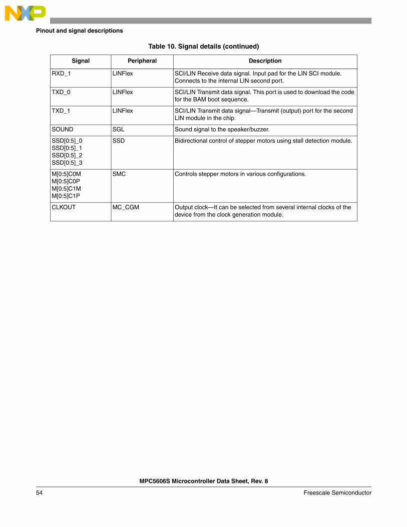
MPC5606S Microcontroller Data Sheet, Rev. 8
Pinout and signal descriptions
Freescale Semiconductor54
RXD_1 LINFlex SCI/LIN Receive data signal. Input pad for the LIN SCI module. Connects to the internal LIN second port.
TXD_0 LINFlex SCI/LIN Transmit data signal. This port is used to download the code for the BAM boot sequence.
TXD_1 LINFlex SCI/LIN Transmit data signal—Transmit (output) port for the second LIN module in the chip.
SOUND SGL Sound signal to the speaker/buzzer.
SSD[0:5]_0SSD[0:5]_1SSD[0:5]_2SSD[0:5]_3
SSD Bidirectional control of stepper motors using stall detection module.
M[0:5]C0MM[0:5]C0PM[0:5]C1MM[0:5]C1P
SMC Controls stepper motors in various configurations.
CLKOUT MC_CGM Output clock—It can be selected from several internal clocks of the device from the clock generation module.
Table 10. Signal details (continued)
Signal Peripheral Description
Electrical characteristics
MPC5606S Microcontroller Data Sheet, Rev. 8
Freescale Semiconductor 55
3 Electrical characteristics
3.1 Introduction
This section contains electrical characteristics of the device as well as temperature and power considerations.
This product contains devices to protect the inputs against damage due to high static voltages. However, it is advisable to take precautions to avoid application of any voltage higher than the specified maximum rated voltages.
To enhance reliability, unused inputs can be driven to an appropriate logic voltage level (VDD or VSS). This could be done by internal pull up and pull down, which is provided by the product for most general purpose pins.
The parameters listed in the following tables represent the characteristics of the device and its demands on the system.
In the tables where the device logic provides signals with their respective timing characteristics, the symbol “CC” for Controller Characteristics is included in the Symbol column.
In the tables where the external system must provide signals with their respective timing characteristics to the device, the symbol “SR” for System Requirement is included in the Symbol column.
3.2 Parameter classificationThe electrical parameters shown in this supplement are guaranteed by various methods. To give the customer a better understanding, the classifications listed in Table 11 are used and the parameters are tagged accordingly in the tables where appropriate.
NOTEThe classification is shown in the column labeled “C” in the parameter tables where appropriate.
3.3 NVUSRO registerPortions of the device configuration, such as high voltage supply, oscillator margin, and watchdog enable/disable after reset are controlled via bit values in the Nonvolatile User Options (NVUSRO) register. For a detailed description of the NVUSRO register, please see the chip reference manual.
3.3.1 NVUSRO[PAD3V5V] field descriptionTable 12 shows how NVUSRO[PAD3V5V] controls the device configuration.
Table 11. Parameter classifications
Classification tag Tag description
P Those parameters are guaranteed during production testing on each individual device.
C Those parameters are achieved by the design characterization by measuring a statistically relevant sample size across process variations.
T Those parameters are achieved by design characterization on a small sample size from typical devices under typical conditions unless otherwise noted. All values shown in the typical column are within this category.
D Those parameters are derived mainly from simulations.
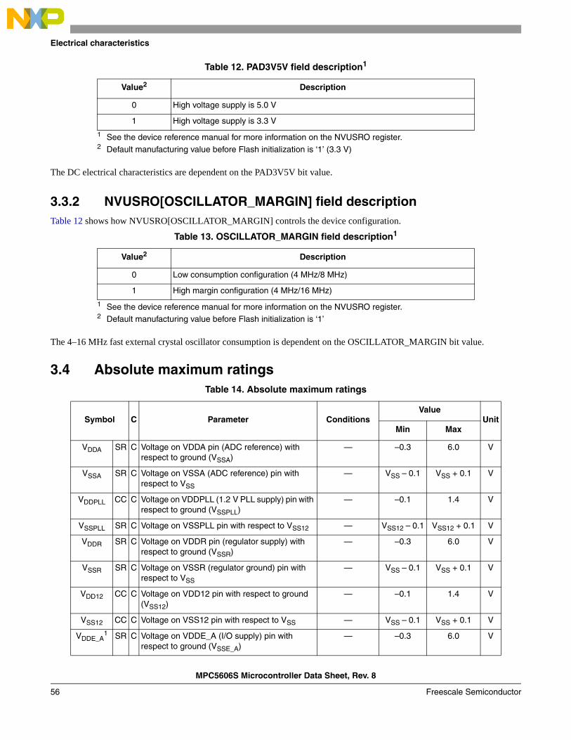
MPC5606S Microcontroller Data Sheet, Rev. 8
Electrical characteristics
Freescale Semiconductor56
The DC electrical characteristics are dependent on the PAD3V5V bit value.
3.3.2 NVUSRO[OSCILLATOR_MARGIN] field descriptionTable 12 shows how NVUSRO[OSCILLATOR_MARGIN] controls the device configuration.
The 4–16 MHz fast external crystal oscillator consumption is dependent on the OSCILLATOR_MARGIN bit value.
3.4 Absolute maximum ratings
Table 12. PAD3V5V field description1
1 See the device reference manual for more information on the NVUSRO register.
Value2
2 Default manufacturing value before Flash initialization is ‘1’ (3.3 V)
Description
0 High voltage supply is 5.0 V
1 High voltage supply is 3.3 V
Table 13. OSCILLATOR_MARGIN field description1
1 See the device reference manual for more information on the NVUSRO register.
Value2
2 Default manufacturing value before Flash initialization is ‘1’
Description
0 Low consumption configuration (4 MHz/8 MHz)
1 High margin configuration (4 MHz/16 MHz)
Table 14. Absolute maximum ratings
Symbol C Parameter ConditionsValue
UnitMin Max
VDDA SR C Voltage on VDDA pin (ADC reference) with respect to ground (VSSA)
— –0.3 6.0 V
VSSA SR C Voltage on VSSA (ADC reference) pin with respect to VSS
— VSS – 0.1 VSS + 0.1 V
VDDPLL CC C Voltage on VDDPLL (1.2 V PLL supply) pin with respect to ground (VSSPLL)
— –0.1 1.4 V
VSSPLL SR C Voltage on VSSPLL pin with respect to VSS12 — VSS12 – 0.1 VSS12 + 0.1 V
VDDR SR C Voltage on VDDR pin (regulator supply) with respect to ground (VSSR)
— –0.3 6.0 V
VSSR SR C Voltage on VSSR (regulator ground) pin with respect to VSS
— VSS – 0.1 VSS + 0.1 V
VDD12 CC C Voltage on VDD12 pin with respect to ground (VSS12)
— –0.1 1.4 V
VSS12 CC C Voltage on VSS12 pin with respect to VSS — VSS – 0.1 VSS + 0.1 V
VDDE_A1 SR C Voltage on VDDE_A (I/O supply) pin with
respect to ground (VSSE_A)— –0.3 6.0 V
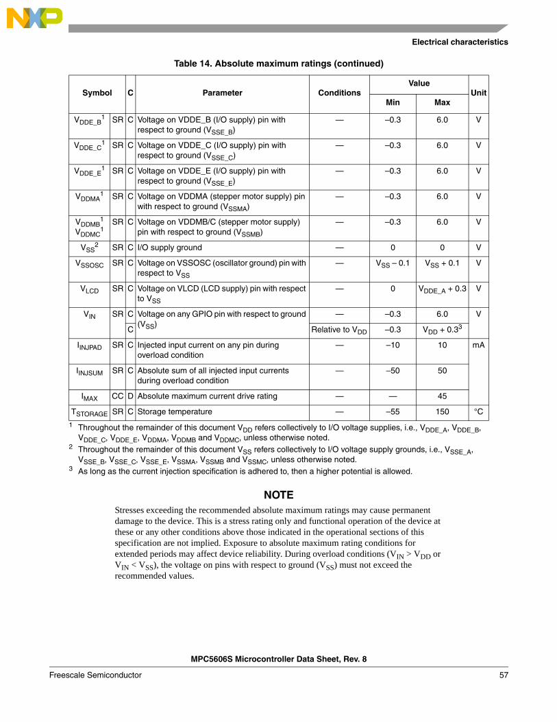
Electrical characteristics
MPC5606S Microcontroller Data Sheet, Rev. 8
Freescale Semiconductor 57
NOTEStresses exceeding the recommended absolute maximum ratings may cause permanent damage to the device. This is a stress rating only and functional operation of the device at these or any other conditions above those indicated in the operational sections of this specification are not implied. Exposure to absolute maximum rating conditions for extended periods may affect device reliability. During overload conditions (VIN > VDD or VIN < VSS), the voltage on pins with respect to ground (VSS) must not exceed the recommended values.
VDDE_B1 SR C Voltage on VDDE_B (I/O supply) pin with
respect to ground (VSSE_B)— –0.3 6.0 V
VDDE_C1 SR C Voltage on VDDE_C (I/O supply) pin with
respect to ground (VSSE_C)— –0.3 6.0 V
VDDE_E1 SR C Voltage on VDDE_E (I/O supply) pin with
respect to ground (VSSE_E)— –0.3 6.0 V
VDDMA1 SR C Voltage on VDDMA (stepper motor supply) pin
with respect to ground (VSSMA)— –0.3 6.0 V
VDDMB1
VDDMC1
SR C Voltage on VDDMB/C (stepper motor supply) pin with respect to ground (VSSMB)
— –0.3 6.0 V
VSS2 SR C I/O supply ground — 0 0 V
VSSOSC SR C Voltage on VSSOSC (oscillator ground) pin with respect to VSS
— VSS – 0.1 VSS + 0.1 V
VLCD SR C Voltage on VLCD (LCD supply) pin with respect to VSS
— 0 VDDE_A + 0.3 V
VIN SR C Voltage on any GPIO pin with respect to ground (VSS)
— –0.3 6.0 V
C Relative to VDD –0.3 VDD + 0.33
IINJPAD SR C Injected input current on any pin during overload condition
— –10 10 mA
IINJSUM SR C Absolute sum of all injected input currents during overload condition
— –50 50
IMAX CC D Absolute maximum current drive rating — — 45
TSTORAGE SR C Storage temperature — –55 150 °C
1 Throughout the remainder of this document VDD refers collectively to I/O voltage supplies, i.e., VDDE_A, VDDE_B, VDDE_C, VDDE_E, VDDMA, VDDMB and VDDMC, unless otherwise noted.
2 Throughout the remainder of this document VSS refers collectively to I/O voltage supply grounds, i.e., VSSE_A, VSSE_B, VSSE_C, VSSE_E, VSSMA, VSSMB and VSSMC, unless otherwise noted.
3 As long as the current injection specification is adhered to, then a higher potential is allowed.
Table 14. Absolute maximum ratings (continued)
Symbol C Parameter ConditionsValue
UnitMin Max
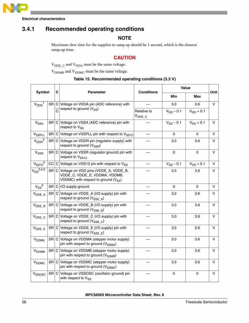
MPC5606S Microcontroller Data Sheet, Rev. 8
Electrical characteristics
Freescale Semiconductor58
3.4.1 Recommended operating conditions
NOTEMaximum slew time for the supplies to ramp up should be 1 second, which is the slowest ramp-up time.
CAUTIONVDDE_C and VDDA must be the same voltage.
VDDMB and VDDMC must be the same voltage.
Table 15. Recommended operating conditions (3.3 V)
Symbol C Parameter ConditionsValue
UnitMin Max
VDDA1 SR C Voltage on VDDA pin (ADC reference) with
respect to ground (VSS)— 3.0 3.6 V
C Relative to VDDE_C
VDD – 0.1 VDD + 0.1
VSSA SR C Voltage on VSSA (ADC reference) pin with respect to VSS
— VSS – 0.1 VSS + 0.1 V
VSSPLL SR C Voltage on VSSPLL pin with respect to VSS12 — 0 0 V
VDDR2 SR C Voltage on VDDR pin (regulator supply) with
respect to ground (VSSR)— 3.0 3.6 V
VSSR SR C Voltage on VSSR (regulator ground) pin with respect to VSS12
— 0 0 V
VSS124 CC C Voltage on VSS12 pin with respect to VSS — VSS – 0.1 VSS + 0.1 V
VDD3,4,5 SR C Voltage on VDD pins (VDDE_A, VDDE_B,
VDDE_C, VDDE_E, VDDMA, VDDMB, VDDMC) with respect to ground (VSS)
— 3.0 3.6 V
VSS6 SR C I/O supply ground — 0 0 V
VDDE_A SR C Voltage on VDDE_A (I/O supply) pin with respect to ground (VSSE_A)
— 3.0 3.6 V
VDDE_B SR C Voltage on VDDE_B (I/O supply) pin with respect to ground (VSSE_B)
— 3.0 3.6 V
VDDE_C SR C Voltage on VDDE_C (I/O supply) pin with respect to ground (VSSE_C)
— 3.0 3.6 V
VDDE_E SR C Voltage on VDDE_E (I/O supply) pin with respect to ground (VSSE_E)
— 3.0 3.6 V
VDDMA SR C Voltage on VDDMA (stepper motor supply) pin with respect to ground (VSSMA)
— 3.0 3.6 V
VDDMB SR C Voltage on VDDMB (stepper motor supply) pin with respect to ground (VSSMB)
— 3.0 3.6 V
VDDMC SR C Voltage on VDDMC (stepper motor supply) pin with respect to ground (VSSMC)
— 3.0 3.6 V
VSSOSC SR C Voltage on VSSOSC (oscillator ground) pin with respect to VSS
— 0 0 V
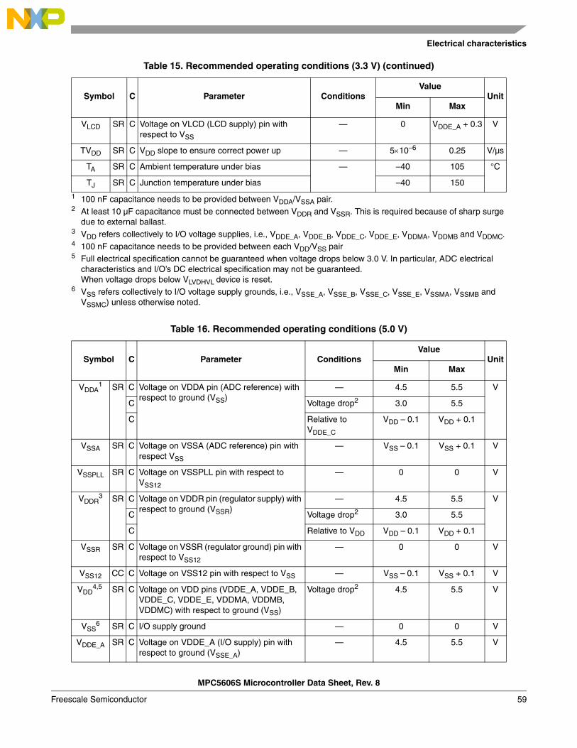
Electrical characteristics
MPC5606S Microcontroller Data Sheet, Rev. 8
Freescale Semiconductor 59
VLCD SR C Voltage on VLCD (LCD supply) pin with respect to VSS
— 0 VDDE_A + 0.3 V
TVDD SR C VDD slope to ensure correct power up — 510–6 0.25 V/µs
TA SR C Ambient temperature under bias — –40 105 °C
TJ SR C Junction temperature under bias –40 150
1 100 nF capacitance needs to be provided between VDDA/VSSA pair.2 At least 10 µF capacitance must be connected between VDDR and VSSR. This is required because of sharp surge
due to external ballast.3 VDD refers collectively to I/O voltage supplies, i.e., VDDE_A, VDDE_B, VDDE_C, VDDE_E, VDDMA, VDDMB and VDDMC.4 100 nF capacitance needs to be provided between each VDD/VSS pair5 Full electrical specification cannot be guaranteed when voltage drops below 3.0 V. In particular, ADC electrical
characteristics and I/O’s DC electrical specification may not be guaranteed.When voltage drops below VLVDHVL device is reset.
6 VSS refers collectively to I/O voltage supply grounds, i.e., VSSE_A, VSSE_B, VSSE_C, VSSE_E, VSSMA, VSSMB and VSSMC) unless otherwise noted.
Table 16. Recommended operating conditions (5.0 V)
Symbol C Parameter ConditionsValue
UnitMin Max
VDDA1 SR C Voltage on VDDA pin (ADC reference) with
respect to ground (VSS)— 4.5 5.5 V
C Voltage drop2 3.0 5.5
C Relative to VDDE_C
VDD – 0.1 VDD + 0.1
VSSA SR C Voltage on VSSA (ADC reference) pin with respect VSS
— VSS – 0.1 VSS + 0.1 V
VSSPLL SR C Voltage on VSSPLL pin with respect to VSS12
— 0 0 V
VDDR3 SR C Voltage on VDDR pin (regulator supply) with
respect to ground (VSSR)— 4.5 5.5 V
C Voltage drop2 3.0 5.5
C Relative to VDD VDD – 0.1 VDD + 0.1
VSSR SR C Voltage on VSSR (regulator ground) pin with respect to VSS12
— 0 0 V
VSS12 CC C Voltage on VSS12 pin with respect to VSS — VSS – 0.1 VSS + 0.1 V
VDD4,5 SR C Voltage on VDD pins (VDDE_A, VDDE_B,
VDDE_C, VDDE_E, VDDMA, VDDMB, VDDMC) with respect to ground (VSS)
Voltage drop2 4.5 5.5 V
VSS6 SR C I/O supply ground — 0 0 V
VDDE_A SR C Voltage on VDDE_A (I/O supply) pin with respect to ground (VSSE_A)
— 4.5 5.5 V
Table 15. Recommended operating conditions (3.3 V) (continued)
Symbol C Parameter ConditionsValue
UnitMin Max
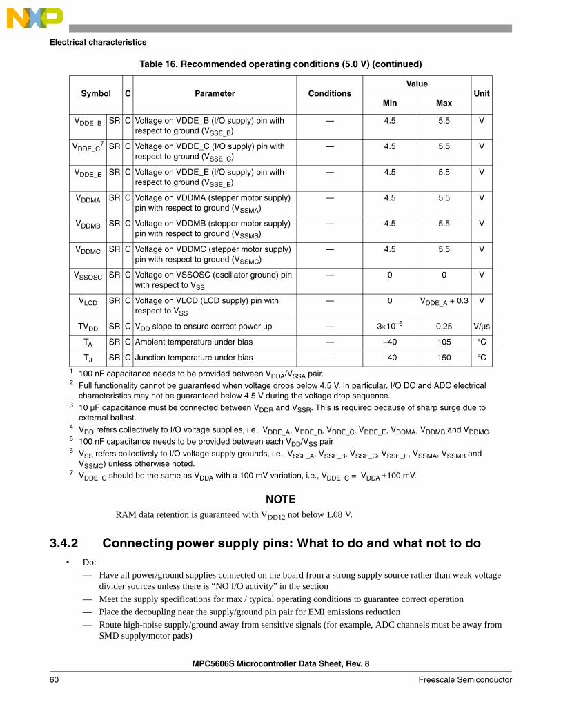
MPC5606S Microcontroller Data Sheet, Rev. 8
Electrical characteristics
Freescale Semiconductor60
NOTERAM data retention is guaranteed with VDD12 not below 1.08 V.
3.4.2 Connecting power supply pins: What to do and what not to do• Do:
— Have all power/ground supplies connected on the board from a strong supply source rather than weak voltage divider sources unless there is “NO I/O activity” in the section
— Meet the supply specifications for max / typical operating conditions to guarantee correct operation
— Place the decoupling near the supply/ground pin pair for EMI emissions reduction
— Route high-noise supply/ground away from sensitive signals (for example, ADC channels must be away from SMD supply/motor pads)
VDDE_B SR C Voltage on VDDE_B (I/O supply) pin with respect to ground (VSSE_B)
— 4.5 5.5 V
VDDE_C7 SR C Voltage on VDDE_C (I/O supply) pin with
respect to ground (VSSE_C)— 4.5 5.5 V
VDDE_E SR C Voltage on VDDE_E (I/O supply) pin with respect to ground (VSSE_E)
— 4.5 5.5 V
VDDMA SR C Voltage on VDDMA (stepper motor supply) pin with respect to ground (VSSMA)
— 4.5 5.5 V
VDDMB SR C Voltage on VDDMB (stepper motor supply) pin with respect to ground (VSSMB)
— 4.5 5.5 V
VDDMC SR C Voltage on VDDMC (stepper motor supply) pin with respect to ground (VSSMC)
— 4.5 5.5 V
VSSOSC SR C Voltage on VSSOSC (oscillator ground) pin with respect to VSS
— 0 0 V
VLCD SR C Voltage on VLCD (LCD supply) pin with respect to VSS
— 0 VDDE_A + 0.3 V
TVDD SR C VDD slope to ensure correct power up — 310–6 0.25 V/µs
TA SR C Ambient temperature under bias — –40 105 °C
TJ SR C Junction temperature under bias — –40 150 °C
1 100 nF capacitance needs to be provided between VDDA/VSSA pair.2 Full functionality cannot be guaranteed when voltage drops below 4.5 V. In particular, I/O DC and ADC electrical
characteristics may not be guaranteed below 4.5 V during the voltage drop sequence.3 10 µF capacitance must be connected between VDDR and VSSR. This is required because of sharp surge due to
external ballast.4 VDD refers collectively to I/O voltage supplies, i.e., VDDE_A, VDDE_B, VDDE_C, VDDE_E, VDDMA, VDDMB and VDDMC.5 100 nF capacitance needs to be provided between each VDD/VSS pair6 VSS refers collectively to I/O voltage supply grounds, i.e., VSSE_A, VSSE_B, VSSE_C, VSSE_E, VSSMA, VSSMB and
VSSMC) unless otherwise noted.7 VDDE_C should be the same as VDDA with a 100 mV variation, i.e., VDDE_C = VDDA 100 mV.
Table 16. Recommended operating conditions (5.0 V) (continued)
Symbol C Parameter ConditionsValue
UnitMin Max
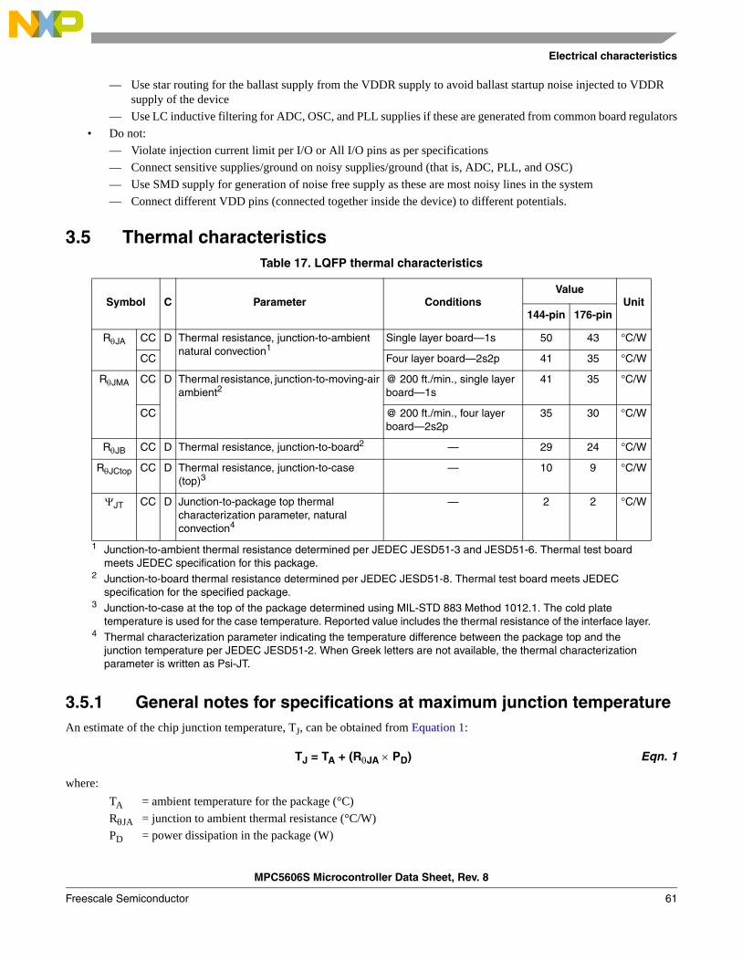
Electrical characteristics
MPC5606S Microcontroller Data Sheet, Rev. 8
Freescale Semiconductor 61
— Use star routing for the ballast supply from the VDDR supply to avoid ballast startup noise injected to VDDR supply of the device
— Use LC inductive filtering for ADC, OSC, and PLL supplies if these are generated from common board regulators
• Do not:
— Violate injection current limit per I/O or All I/O pins as per specifications
— Connect sensitive supplies/ground on noisy supplies/ground (that is, ADC, PLL, and OSC)
— Use SMD supply for generation of noise free supply as these are most noisy lines in the system
— Connect different VDD pins (connected together inside the device) to different potentials.
3.5 Thermal characteristics
3.5.1 General notes for specifications at maximum junction temperatureAn estimate of the chip junction temperature, TJ, can be obtained from Equation 1:
TJ = TA + (RJA PD) Eqn. 1
where:
TA = ambient temperature for the package (°C)
RJA = junction to ambient thermal resistance (°C/W)
PD = power dissipation in the package (W)
Table 17. LQFP thermal characteristics
Symbol C Parameter ConditionsValue
Unit144-pin 176-pin
RJA CC D Thermal resistance, junction-to-ambient natural convection1
1 Junction-to-ambient thermal resistance determined per JEDEC JESD51-3 and JESD51-6. Thermal test board meets JEDEC specification for this package.
Single layer board—1s 50 43 °C/W
CC Four layer board—2s2p 41 35 °C/W
RJMA CC D Thermal resistance, junction-to-moving-air ambient2
@ 200 ft./min., single layerboard—1s
41 35 °C/W
CC @ 200 ft./min., four layerboard—2s2p
35 30 °C/W
RJB CC D Thermal resistance, junction-to-board2
2 Junction-to-board thermal resistance determined per JEDEC JESD51-8. Thermal test board meets JEDEC specification for the specified package.
— 29 24 °C/W
RJCtop CC D Thermal resistance, junction-to-case (top)3
3 Junction-to-case at the top of the package determined using MIL-STD 883 Method 1012.1. The cold plate temperature is used for the case temperature. Reported value includes the thermal resistance of the interface layer.
— 10 9 °C/W
JT CC D Junction-to-package top thermal characterization parameter, natural convection4
4 Thermal characterization parameter indicating the temperature difference between the package top and the junction temperature per JEDEC JESD51-2. When Greek letters are not available, the thermal characterization parameter is written as Psi-JT.
— 2 2 °C/W
MPC5606S Microcontroller Data Sheet, Rev. 8
Electrical characteristics
Freescale Semiconductor62
The thermal resistance values used are based on the JEDEC JESD51 series of standards to provide consistent values for estimations and comparisons. The difference between the values determined for the single-layer (1s) board compared to a four-layer board that has two signal layers, a power and a ground plane (2s2p), demonstrate that the effective thermal resistance is not a constant. The thermal resistance depends on the:
• Construction of the application board (number of planes)
• Effective size of the board that cools the component
• Quality of the thermal and electrical connections to the planes
• Power dissipated by adjacent components
Connect all the ground and power balls to the respective planes with one via per ball. Using fewer vias to connect the package to the planes reduces the thermal performance. Thinner planes also reduce the thermal performance. When the clearance between the vias leave the planes virtually disconnected, the thermal performance is also greatly reduced.
As a general rule, the value obtained on a single-layer board is within the normal range for the tightly packed printed circuit board. The value obtained on a board with the internal planes is usually within the normal range if the application board has:
• One oz. (35 micron nominal thickness) internal planes
• Components are well separated
• Overall power dissipation on the board is less than 0.02 W/cm2
The thermal performance of any component depends on the power dissipation of the surrounding components. In addition, the ambient temperature varies widely within the application. For many natural convection and especially closed box applications, the board temperature at the perimeter (edge) of the package is approximately the same as the local air temperature near the device. Specifying the local ambient conditions explicitly as the board temperature provides a more precise description of the local ambient conditions that determine the temperature of the device.
At a known board temperature, the junction temperature is estimated using Equation 2:
TJ = TB + (RJB PD) Eqn. 2
where:
TB = board temperature for the package perimeter (°C)
RJB = junction-to-board thermal resistance (°C/W) per JESD51-8S
PD = power dissipation in the package (W)
When the heat loss from the package case to the air does not factor into the calculation, an acceptable value for the junction temperature is predictable. Ensure the application board is similar to the thermal test condition, with the component soldered to a board with internal planes.
The thermal resistance is expressed as the sum of a junction-to-case thermal resistance plus a case-to-ambient thermal resistance:
RJA = RJC + RCA Eqn. 3
where:
RJA = junction to ambient thermal resistance (°C/W)
RJC = junction to case thermal resistance (°C/W)
RCA = case to ambient thermal resistance (°C/W)
RJC s device related and is not affected by other factors. The thermal environment can be controlled to change the case-to-ambient thermal resistance, RCA. For example, change the air flow around the device, add a heat sink, change the mounting arrangement on the printed circuit board, or change the thermal dissipation on the printed circuit board surrounding the device. This description is most useful for packages with heat sinks where 90% of the heat flow is through the case to heat sink to ambient. For most packages, a better model is required.
Electrical characteristics
MPC5606S Microcontroller Data Sheet, Rev. 8
Freescale Semiconductor 63
A more accurate two-resistor thermal model can be constructed from the junction-to-board thermal resistance and the junction-to-case thermal resistance. The junction-to-case thermal resistance describes when using a heat sink or where a substantial amount of heat is dissipated from the top of the package. The junction-to-board thermal resistance describes the thermal performance when most of the heat is conducted to the printed circuit board. This model can be used to generate simple estimations and for computational fluid dynamics (CFD) thermal models.
To determine the junction temperature of the device in the application on a prototype board, use the thermal characterization parameter (JT) to determine the junction temperature by measuring the temperature at the top center of the package case using Equation 4:
TJ = TT + (JT x PD) Eqn. 4
where:
TT = thermocouple temperature on top of the package (°C)
JT = thermal characterization parameter (°C/W)
PD = power dissipation in the package (W)
The thermal characterization parameter is measured in compliance with the JESD51-2 specification using a 40-gauge type T thermocouple epoxied to the top center of the package case. Position the thermocouple so that the thermocouple junction rests on the package. Place a small amount of epoxy on the thermocouple junction and approximately 1 mm of wire extending from the junction. Place the thermocouple wire flat against the package case to avoid measurement errors caused by the cooling effects of the thermocouple wire.
References:
Semiconductor Equipment and Materials International805 East Middlefield Rd.Mountain View, CA 94043 USA(415) 964-5111
MIL-SPEC and EIA/JESD (JEDEC) specifications are available from Global Engineering Documents at 800-854-7179 or 303-397-7956.
JEDEC specifications are available on the WEB at http://www.jedec.org.
3.6 Electromagnetic compatibility (EMC) characteristicsSusceptibility tests are performed on a sample basis during product characterization.
3.6.1 EMC requirements on boardThe following practices help minimize noise in applications.
• Place a 100 nF capacitor between each of the VDD12/VSS12 supply pairs and also between the VDDPLL/VSSPLL pair. The voltage regulator also requires stability capacitors for these supply pairs.
• Place a 10 µF capacitor on VDDR.
• Isolate VDDR with ballast emitter to avoid voltage droop during STANDBY mode exit.
• Enable pad slew rate only as necessary to eliminate I/O noise:
— Enabling slew rate for SMD pads will reduce noise on motors.
— Disabling slew rate for non-SMD pads will reduce noise on non-SMD I/Os.
• Enable PLL modulation (± 2%) for system clock.
• Place decoupling capacitors for all HV supplies close to the pins.
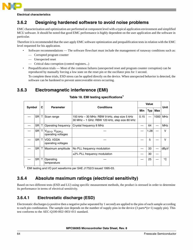
MPC5606S Microcontroller Data Sheet, Rev. 8
Electrical characteristics
Freescale Semiconductor64
3.6.2 Designing hardened software to avoid noise problemsEMC characterization and optimization are performed at component level with a typical application environment and simplified MCU software. It should be noted that good EMC performance is highly dependent on the user application and the software in particular.
Therefore it is recommended that the user apply EMC software optimization and prequalification tests in relation with the EMC level requested for his application.
• Software recommendations — The software flowchart must include the management of runaway conditions such as:
— Corrupted program counter
— Unexpected reset
— Critical data corruption (control registers...)
• Prequalification trials — Most of the common failures (unexpected reset and program counter corruption) can be reproduced by manually forcing a low state on the reset pin or the oscillator pins for 1 second.
To complete these trials, ESD stress can be applied directly on the device. When unexpected behavior is detected, the software can be hardened to prevent unrecoverable errors occurring.
3.6.3 Electromagnetic interference (EMI)
3.6.4 Absolute maximum ratings (electrical sensitivity)Based on two different tests (ESD and LU) using specific measurement methods, the product is stressed in order to determine its performance in terms of electrical sensitivity.
3.6.4.1 Electrostatic discharge (ESD)Electrostatic discharges (a positive then a negative pulse separated by 1 second) are applied to the pins of each sample according to each pin combination. The sample size depends on the number of supply pins in the device (3 parts*(n+1) supply pin). This test conforms to the AEC-Q100-002/-003/-011 standard.
Table 18. EMI testing specifications1
1 EMI testing and I/O port waveforms per SAE J1752/3 issued 1995-03.
Symbol C Parameter ConditionsValue
UnitMin Typ Max
— SR T Scan range 150 kHz – 30 MHz: RBW 9 kHz, step size 5 kHz30 MHz – 1 GHz: RBW 120 kHz, step size 80 kHz
0.15 — 1000 MHz
— SR T Operating frequency Crystal frequency 8 MHz — 64 — MHz
— SR T VDD12, VDDPLL operating voltages
— — 1.28 — V
— SR T VDD, VDDA operating voltages
— — 5 — V
— SR T Maximum amplitude No PLL frequency modulation — 33 — dBµV
±2% PLL frequency modulation — 30 —
— SR T Operating temperature
— — 25 — °C
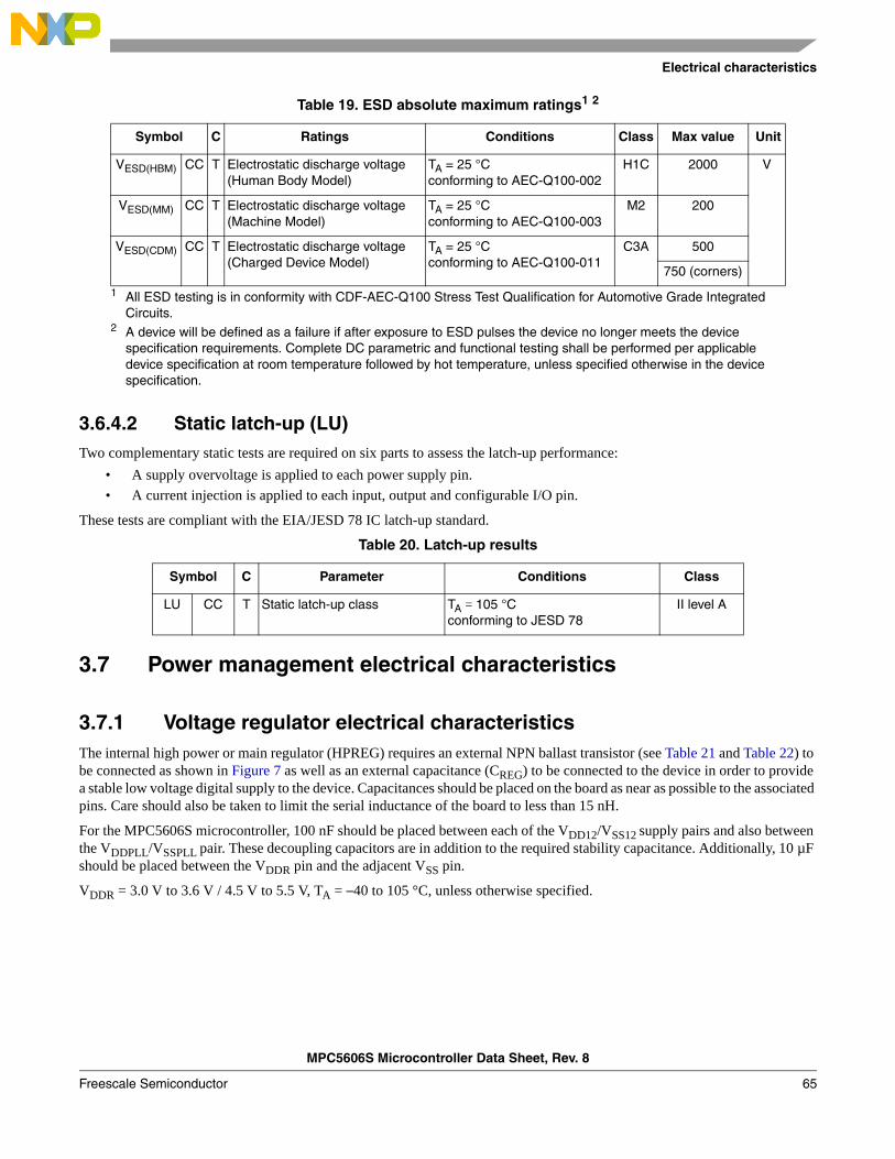
Electrical characteristics
MPC5606S Microcontroller Data Sheet, Rev. 8
Freescale Semiconductor 65
3.6.4.2 Static latch-up (LU)Two complementary static tests are required on six parts to assess the latch-up performance:
• A supply overvoltage is applied to each power supply pin.
• A current injection is applied to each input, output and configurable I/O pin.
These tests are compliant with the EIA/JESD 78 IC latch-up standard.
3.7 Power management electrical characteristics
3.7.1 Voltage regulator electrical characteristicsThe internal high power or main regulator (HPREG) requires an external NPN ballast transistor (see Table 21 and Table 22) to be connected as shown in Figure 7 as well as an external capacitance (CREG) to be connected to the device in order to provide a stable low voltage digital supply to the device. Capacitances should be placed on the board as near as possible to the associated pins. Care should also be taken to limit the serial inductance of the board to less than 15 nH.
For the MPC5606S microcontroller, 100 nF should be placed between each of the VDD12/VSS12 supply pairs and also between the VDDPLL/VSSPLL pair. These decoupling capacitors are in addition to the required stability capacitance. Additionally, 10 µF should be placed between the VDDR pin and the adjacent VSS pin.
VDDR = 3.0 V to 3.6 V / 4.5 V to 5.5 V, TA = –40 to 105 °C, unless otherwise specified.
Table 19. ESD absolute maximum ratings1 2
1 All ESD testing is in conformity with CDF-AEC-Q100 Stress Test Qualification for Automotive Grade Integrated Circuits.
2 A device will be defined as a failure if after exposure to ESD pulses the device no longer meets the device specification requirements. Complete DC parametric and functional testing shall be performed per applicable device specification at room temperature followed by hot temperature, unless specified otherwise in the device specification.
Symbol C Ratings Conditions Class Max value Unit
VESD(HBM) CC T Electrostatic discharge voltage(Human Body Model)
TA = 25 °Cconforming to AEC-Q100-002
H1C 2000 V
VESD(MM) CC T Electrostatic discharge voltage(Machine Model)
TA = 25 °Cconforming to AEC-Q100-003
M2 200
VESD(CDM) CC T Electrostatic discharge voltage(Charged Device Model)
TA = 25 °Cconforming to AEC-Q100-011
C3A 500
750 (corners)
Table 20. Latch-up results
Symbol C Parameter Conditions Class
LU CC T Static latch-up class TA = 105 °Cconforming to JESD 78
II level A
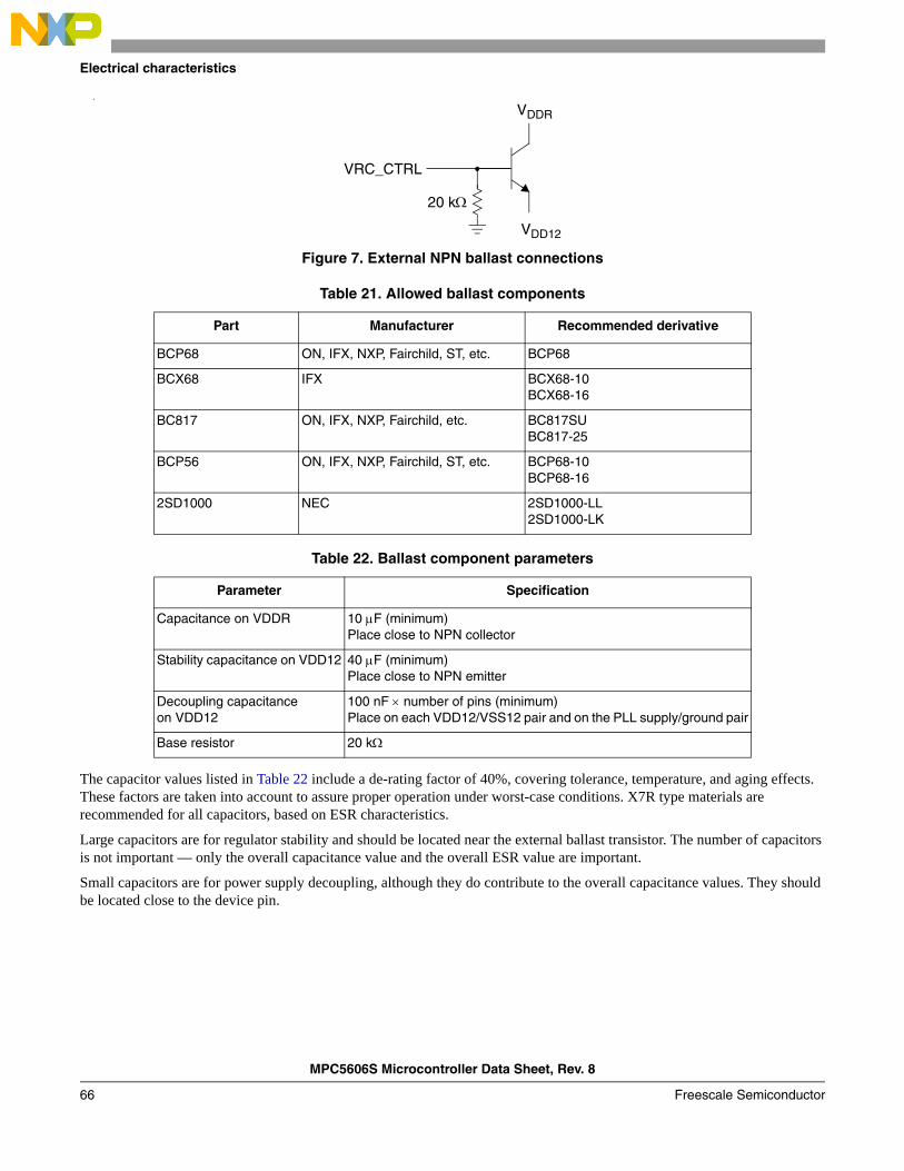
MPC5606S Microcontroller Data Sheet, Rev. 8
Electrical characteristics
Freescale Semiconductor66
a
Figure 7. External NPN ballast connections
The capacitor values listed in Table 22 include a de-rating factor of 40%, covering tolerance, temperature, and aging effects. These factors are taken into account to assure proper operation under worst-case conditions. X7R type materials are recommended for all capacitors, based on ESR characteristics.
Large capacitors are for regulator stability and should be located near the external ballast transistor. The number of capacitors is not important — only the overall capacitance value and the overall ESR value are important.
Small capacitors are for power supply decoupling, although they do contribute to the overall capacitance values. They should be located close to the device pin.
Table 21. Allowed ballast components
Part Manufacturer Recommended derivative
BCP68 ON, IFX, NXP, Fairchild, ST, etc. BCP68
BCX68 IFX BCX68-10BCX68-16
BC817 ON, IFX, NXP, Fairchild, etc. BC817SUBC817-25
BCP56 ON, IFX, NXP, Fairchild, ST, etc. BCP68-10BCP68-16
2SD1000 NEC 2SD1000-LL2SD1000-LK
Table 22. Ballast component parameters
Parameter Specification
Capacitance on VDDR 10 F (minimum)Place close to NPN collector
Stability capacitance on VDD12 40 F (minimum)Place close to NPN emitter
Decoupling capacitance on VDD12
100 nF number of pins (minimum)Place on each VDD12/VSS12 pair and on the PLL supply/ground pair
Base resistor 20 k
VRC_CTRL
VDDR
VDD12
20 k
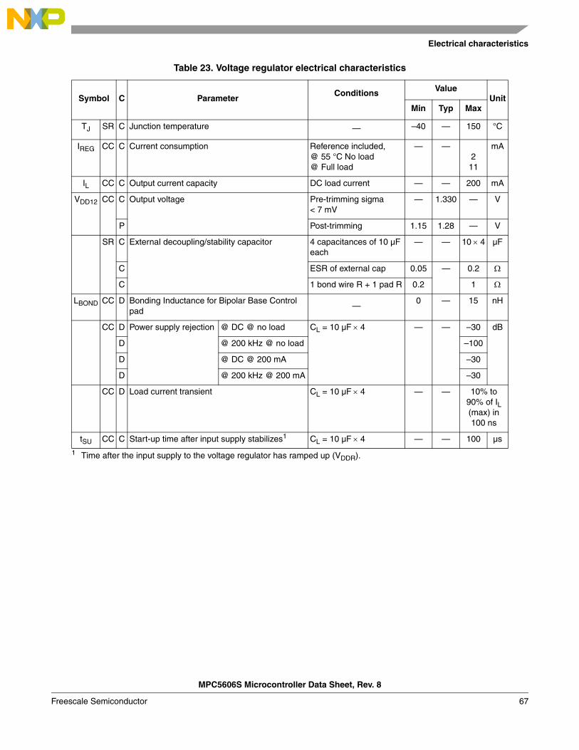
Electrical characteristics
MPC5606S Microcontroller Data Sheet, Rev. 8
Freescale Semiconductor 67
Table 23. Voltage regulator electrical characteristics
Symbol C ParameterConditions Value
UnitMin Typ Max
TJ SR C Junction temperature — –40 — 150 °C
IREG CC C Current consumption Reference included,@ 55 °C No load@ Full load
— —2
11
mA
IL CC C Output current capacity DC load current — — 200 mA
VDD12 CC C Output voltage Pre-trimming sigma < 7 mV
— 1.330 — V
P Post-trimming 1.15 1.28 — V
SR C External decoupling/stability capacitor
4 capacitances of 10 µF each
— — 10 4 µF
C ESR of external cap 0.05 — 0.2
C 1 bond wire R + 1 pad R 0.2 1
LBOND CC D Bonding Inductance for Bipolar Base Control pad
—0 — 15 nH
CC D Power supply rejection @ DC @ no load CL = 10 µF 4 — — –30 dB
D @ 200 kHz @ no load –100
D @ DC @ 200 mA –30
D @ 200 kHz @ 200 mA –30
CC D Load current transient CL = 10 µF 4 — — 10% to 90% of IL (max) in 100 ns
tSU CC C Start-up time after input supply stabilizes1
1 Time after the input supply to the voltage regulator has ramped up (VDDR).
CL = 10 µF 4 — — 100 µs
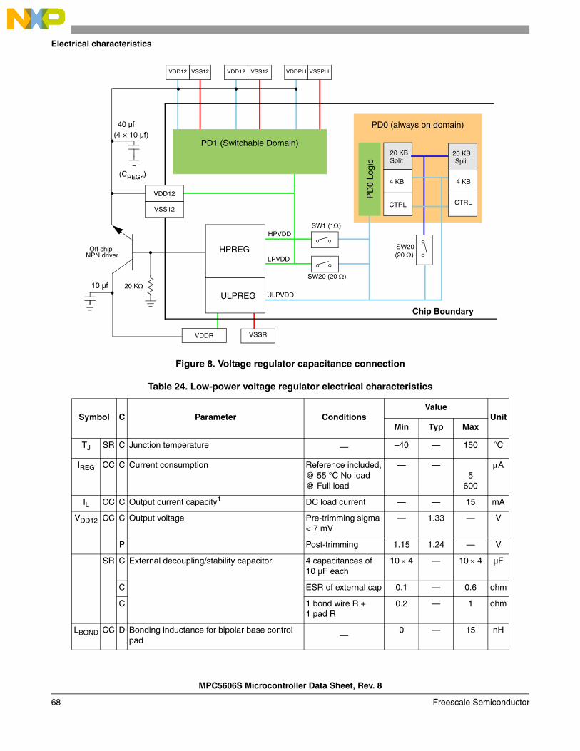
MPC5606S Microcontroller Data Sheet, Rev. 8
Electrical characteristics
Freescale Semiconductor68
Figure 8. Voltage regulator capacitance connection
Table 24. Low-power voltage regulator electrical characteristics
Symbol C Parameter ConditionsValue
UnitMin Typ Max
TJ SR C Junction temperature — –40 — 150 °C
IREG CC C Current consumption Reference included,@ 55 °C No load@ Full load
— —5
600
A
IL CC C Output current capacity1 DC load current — — 15 mA
VDD12 CC C Output voltage Pre-trimming sigma< 7 mV
— 1.33 — V
P Post-trimming 1.15 1.24 — V
SR C External decoupling/stability capacitor 4 capacitances of10 µF each
10 4 — 10 4 µF
C ESR of external cap 0.1 — 0.6 ohm
C 1 bond wire R + 1 pad R
0.2 — 1 ohm
LBOND CC D Bonding inductance for bipolar base control pad
—0 — 15 nH
20 KB
PD0 (always on domain)
PD1 (Switchable Domain)
HPREG
ULPREG
HPVDD
LPVDD
Off chipNPN driver
40 µf
SW1 (1)
VDDR VSSR
VDD12 VDD12 VDDPLLVSS12 VSS12
(CREGn)
Chip Boundary
10 µf
(4 × 10 µf)
VSSPLL
VDD12
VSS12
Split
SW20 (20 )
20 KBSplit
ULPVDD
SW20
CTRL
4 KB
CTRL
4 KB
(20 )
20 K
PD
0 Lo
gic
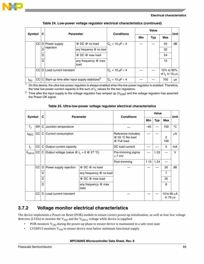
Electrical characteristics
MPC5606S Microcontroller Data Sheet, Rev. 8
Freescale Semiconductor 69
3.7.2 Voltage monitor electrical characteristicsThe device implements a Power-on Reset (POR) module to ensure correct power-up initialization, as well as four low voltage detectors (LVDs) to monitor the VDD and the VDD12 voltage while device is supplied:
• POR monitors VDD during the power-up phase to ensure device is maintained in a safe reset state
• LVDHV3 monitors VDD to ensure device reset below minimum functional supply
CC D Power supply rejection
@ DC @ no load CL = 10 µF 4 — — 55 dB
D any frequency @ no load 32
D @ DC @ max load 24
D any frequency @ max load
12
CC D Load current transient CL = 10 µF 4 — — 10% to 90% of IL in 10 s
tSU CC C Start-up time after input supply stabilizes2 CL = 10 µF 4 — — 700 µs
1 On this device, the ultra-low-power regulator is always enabled when the low-power regulator is enabled. Therefore, the total low-power current capacity is the sum of IL values for the two regulators.
2 Time after the input supply to the voltage regulator has ramped up (VDDR) and the voltage regulator has asserted the Power OK signal.
Table 25. Ultra-low-power voltage regulator electrical characteristics
Symbol C Parameter ConditionsValue
UnitMin Typ Max
TJ SR C Junction temperature — –40 — 150 °C
IREG CC C Current consumption Reference included,@ 55 °C No load@ Full load
— —2
100
A
IL CC C Output current capacity DC load current — — 5 mA
VDD12 CC C Output voltage (value @ IL = 0 @ 27 °C) Pre-trimming sigma < 7 mV
— 1.33 — V
Post-trimming 1.15 1.24 —
CC D Power supply rejection @ DC @ no load — — — 25 dB
D any frequency @ no load 7
D @ DC @ max load 25
D any frequency @ max load
8
CC D Load current transient — — — 10 to 90 A in 70 s
Table 24. Low-power voltage regulator electrical characteristics (continued)
Symbol C Parameter ConditionsValue
UnitMin Typ Max
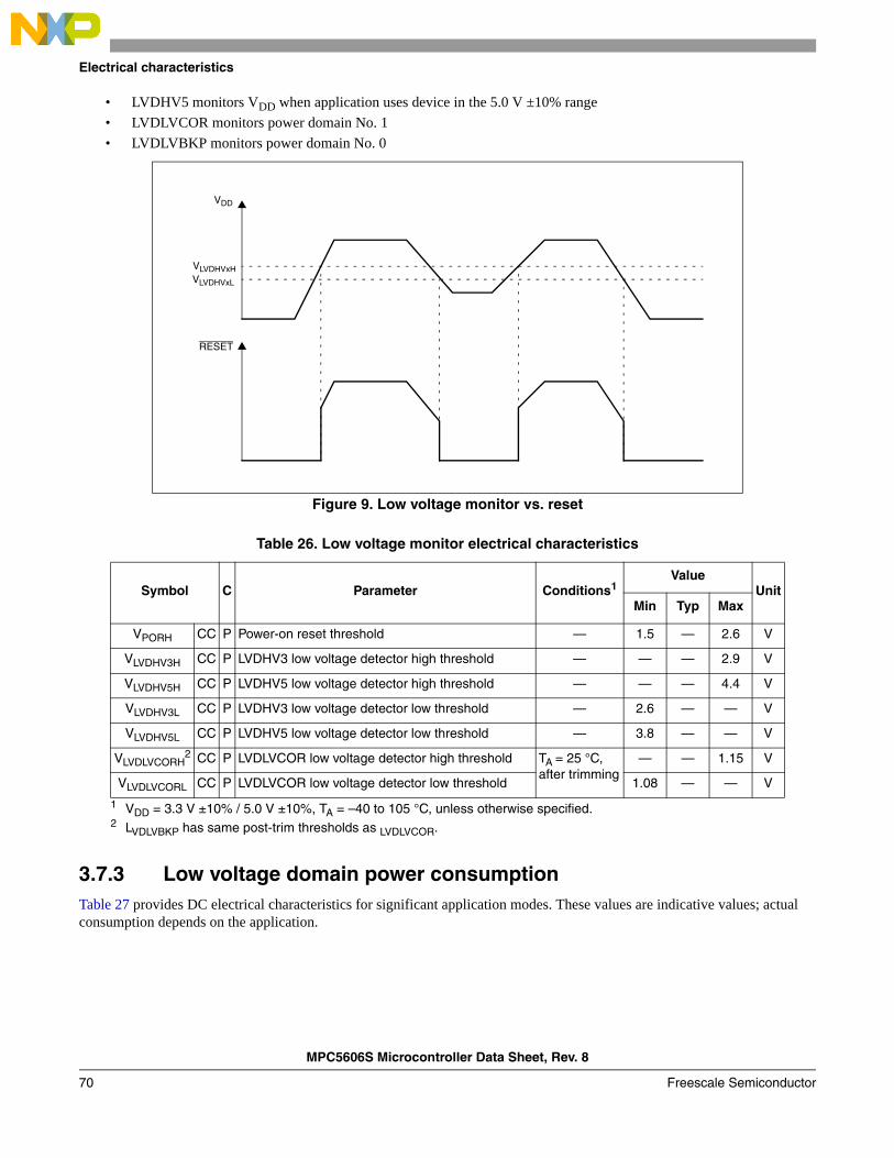
MPC5606S Microcontroller Data Sheet, Rev. 8
Electrical characteristics
Freescale Semiconductor70
• LVDHV5 monitors VDD when application uses device in the 5.0 V ±10% range
• LVDLVCOR monitors power domain No. 1
• LVDLVBKP monitors power domain No. 0
Figure 9. Low voltage monitor vs. reset
3.7.3 Low voltage domain power consumptionTable 27 provides DC electrical characteristics for significant application modes. These values are indicative values; actual consumption depends on the application.
Table 26. Low voltage monitor electrical characteristics
Symbol C Parameter Conditions1
1 VDD = 3.3 V ±10% / 5.0 V ±10%, TA = –40 to 105 °C, unless otherwise specified.
ValueUnit
Min Typ Max
VPORH CC P Power-on reset threshold — 1.5 — 2.6 V
VLVDHV3H CC P LVDHV3 low voltage detector high threshold — — — 2.9 V
VLVDHV5H CC P LVDHV5 low voltage detector high threshold — — — 4.4 V
VLVDHV3L CC P LVDHV3 low voltage detector low threshold — 2.6 — — V
VLVDHV5L CC P LVDHV5 low voltage detector low threshold — 3.8 — — V
VLVDLVCORH2
2 LVDLVBKP has same post-trim thresholds as LVDLVCOR.
CC P LVDLVCOR low voltage detector high threshold TA = 25 °C,after trimming
— — 1.15 V
VLVDLVCORL CC P LVDLVCOR low voltage detector low threshold 1.08 — — V
VDD
VLVDHVxH
RESET
VLVDHVxL
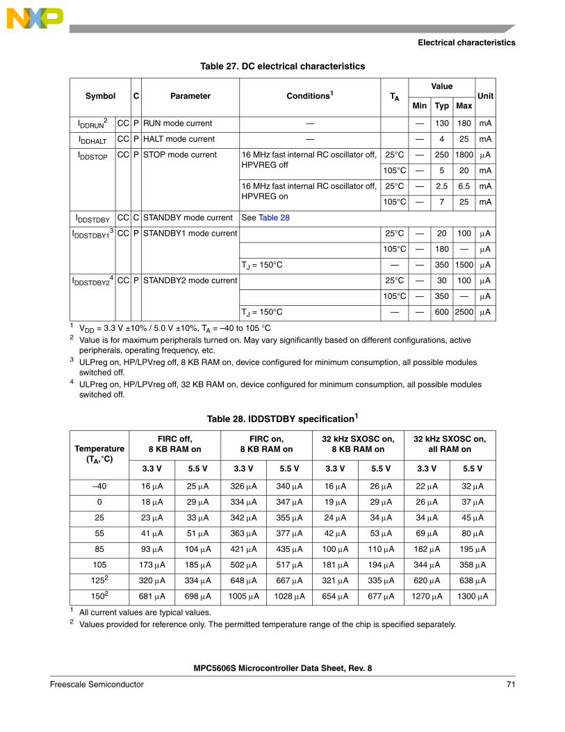
Electrical characteristics
MPC5606S Microcontroller Data Sheet, Rev. 8
Freescale Semiconductor 71
Table 27. DC electrical characteristics
Symbol C Parameter Conditions1
1 VDD = 3.3 V ±10% / 5.0 V ±10%, TA = –40 to 105 °C
TA
ValueUnit
Min Typ Max
IDDRUN2
2 Value is for maximum peripherals turned on. May vary significantly based on different configurations, active peripherals, operating frequency, etc.
CC P RUN mode current — — 130 180 mA
IDDHALT CC P HALT mode current — — 4 25 mA
IDDSTOP CC P STOP mode current 16 MHz fast internal RC oscillator off, HPVREG off
25°C — 250 1800 A
105°C — 5 20 mA
16 MHz fast internal RC oscillator off, HPVREG on
25°C — 2.5 6.5 mA
105°C — 7 25 mA
IDDSTDBY CC C STANDBY mode current See Table 28
IDDSTDBY13
3 ULPreg on, HP/LPVreg off, 8 KB RAM on, device configured for minimum consumption, all possible modules switched off.
CC P STANDBY1 mode current 25°C — 20 100 A
105°C — 180 — A
TJ = 150°C — — 350 1500 A
IDDSTDBY24
4 ULPreg on, HP/LPVreg off, 32 KB RAM on, device configured for minimum consumption, all possible modules switched off.
CC P STANDBY2 mode current 25°C — 30 100 A
105°C — 350 — A
TJ = 150°C — — 600 2500 A
Table 28. IDDSTDBY specification1
1 All current values are typical values.
Temperature (TA,°C)
FIRC off,8 KB RAM on
FIRC on,8 KB RAM on
32 kHz SXOSC on,8 KB RAM on
32 kHz SXOSC on,all RAM on
3.3 V 5.5 V 3.3 V 5.5 V 3.3 V 5.5 V 3.3 V 5.5 V
–40 16 A 25 A 326 A 340 A 16 A 26 A 22 A 32 A
0 18 A 29 A 334 A 347 A 19 A 29 A 26 A 37 A
25 23 A 33 A 342 A 355 A 24 A 34 A 34 A 45 A
55 41 A 51 A 363 A 377 A 42 A 53 A 69 A 80 A
85 93 A 104 A 421 A 435 A 100 A 110 A 182 A 195 A
105 173 A 185 A 502 A 517 A 181 A 194 A 344 A 358 A
1252
2 Values provided for reference only. The permitted temperature range of the chip is specified separately.
320 A 334 A 648 A 667 A 321 A 335 A 620 A 638 A
1502 681 A 698 A 1005 A 1028 A 654 A 677 A 1270 A 1300 A
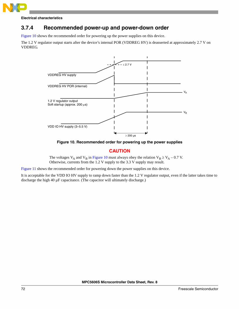
MPC5606S Microcontroller Data Sheet, Rev. 8
Electrical characteristics
Freescale Semiconductor72
3.7.4 Recommended power-up and power-down orderFigure 10 shows the recommended order for powering up the power supplies on this device.
The 1.2 V regulator output starts after the device’s internal POR (VDDREG HV) is deasserted at approximately 2.7 V on VDDREG.
Figure 10. Recommended order for powering up the power supplies
CAUTIONThe voltages VA and VB in Figure 10 must always obey the relation VB VA – 0.7 V. Otherwise, currents from the 1.2 V supply to the 3.3 V supply may result.
Figure 11 shows the recommended order for powering down the power supplies on this device.
It is acceptable for the VDD IO HV supply to ramp down faster than the 1.2 V regulator output, even if the latter takes time to discharge the high 40 µF capacitance. (The capacitor will ultimately discharge.)
VDDREG HV supply
VDDREG HV POR (internal)
1.2 V regulator outputSoft startup (approx. 200 s)
VDD IO HV supply (3–5.5 V)
2.7 V
200 µs
VA
VB
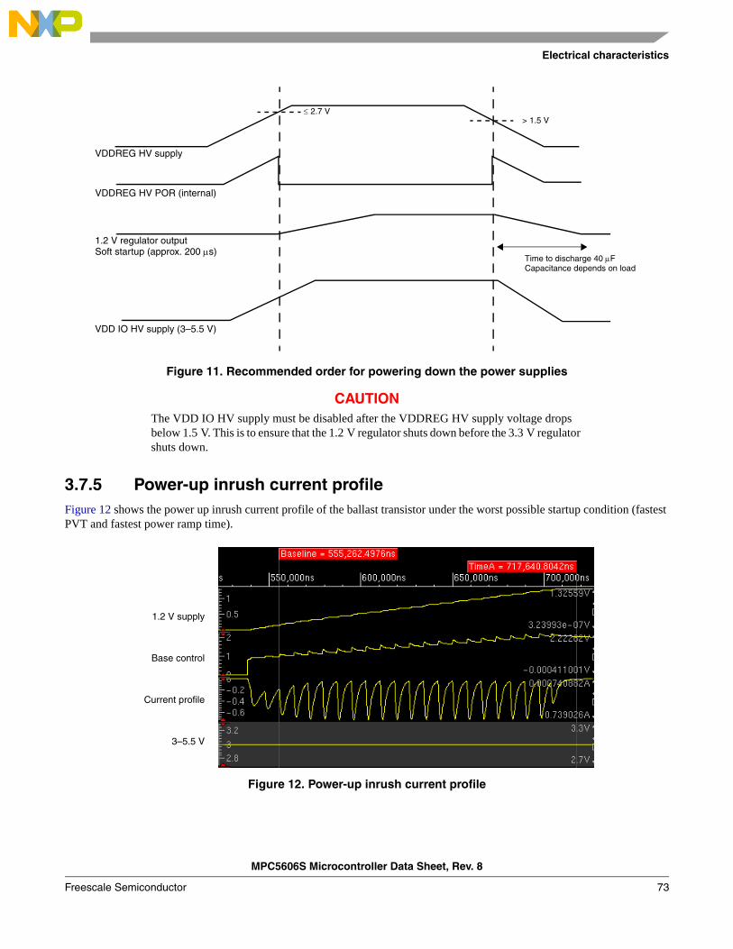
Electrical characteristics
MPC5606S Microcontroller Data Sheet, Rev. 8
Freescale Semiconductor 73
Figure 11. Recommended order for powering down the power supplies
CAUTIONThe VDD IO HV supply must be disabled after the VDDREG HV supply voltage drops below 1.5 V. This is to ensure that the 1.2 V regulator shuts down before the 3.3 V regulator shuts down.
3.7.5 Power-up inrush current profileFigure 12 shows the power up inrush current profile of the ballast transistor under the worst possible startup condition (fastest PVT and fastest power ramp time).
Figure 12. Power-up inrush current profile
VDDREG HV supply
2.7 V
VDDREG HV POR (internal)
1.2 V regulator outputSoft startup (approx. 200 s)
VDD IO HV supply (3–5.5 V)
> 1.5 V
Time to discharge 40 FCapacitance depends on load
1.2 V supply
Base control
Current profile
3–5.5 V
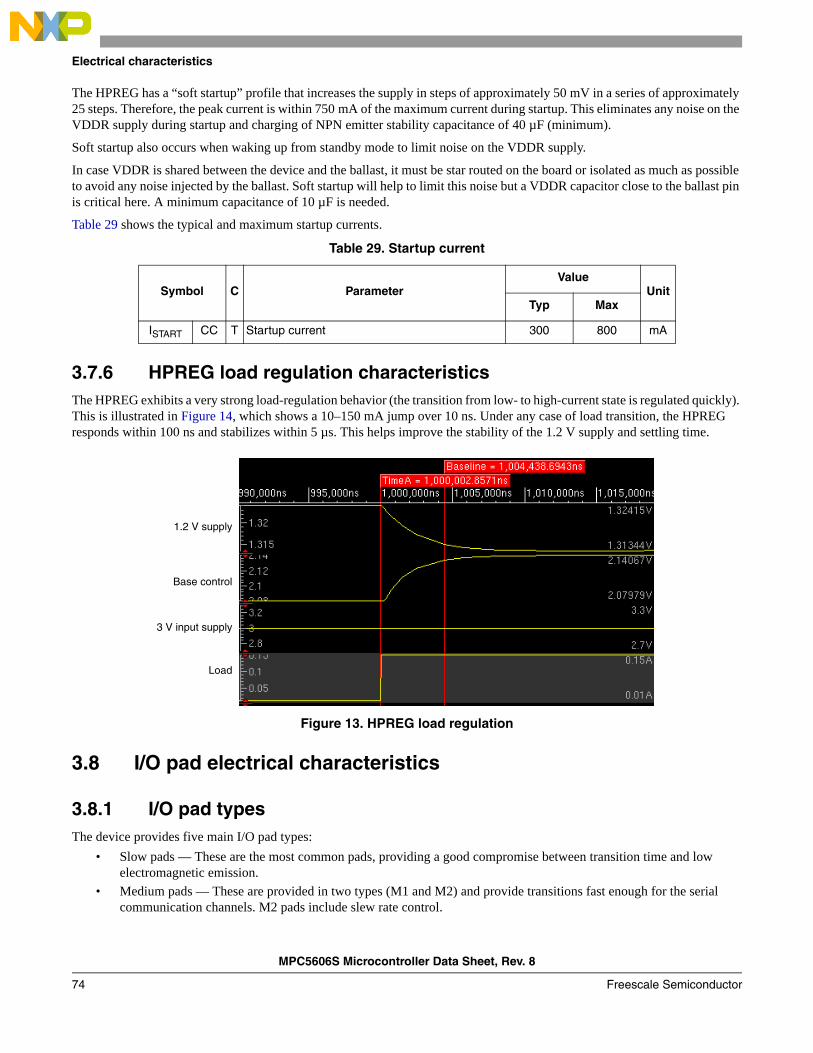
MPC5606S Microcontroller Data Sheet, Rev. 8
Electrical characteristics
Freescale Semiconductor74
The HPREG has a “soft startup” profile that increases the supply in steps of approximately 50 mV in a series of approximately 25 steps. Therefore, the peak current is within 750 mA of the maximum current during startup. This eliminates any noise on the VDDR supply during startup and charging of NPN emitter stability capacitance of 40 µF (minimum).
Soft startup also occurs when waking up from standby mode to limit noise on the VDDR supply.
In case VDDR is shared between the device and the ballast, it must be star routed on the board or isolated as much as possible to avoid any noise injected by the ballast. Soft startup will help to limit this noise but a VDDR capacitor close to the ballast pin is critical here. A minimum capacitance of 10 µF is needed.
Table 29 shows the typical and maximum startup currents.
3.7.6 HPREG load regulation characteristicsThe HPREG exhibits a very strong load-regulation behavior (the transition from low- to high-current state is regulated quickly). This is illustrated in Figure 14, which shows a 10–150 mA jump over 10 ns. Under any case of load transition, the HPREG responds within 100 ns and stabilizes within 5 µs. This helps improve the stability of the 1.2 V supply and settling time.
Figure 13. HPREG load regulation
3.8 I/O pad electrical characteristics
3.8.1 I/O pad typesThe device provides five main I/O pad types:
• Slow pads — These are the most common pads, providing a good compromise between transition time and low electromagnetic emission.
• Medium pads — These are provided in two types (M1 and M2) and provide transitions fast enough for the serial communication channels. M2 pads include slew rate control.
Table 29. Startup current
Symbol C ParameterValue
UnitTyp Max
ISTART CC T Startup current 300 800 mA
1.2 V supply
Base control
3 V input supply
Load
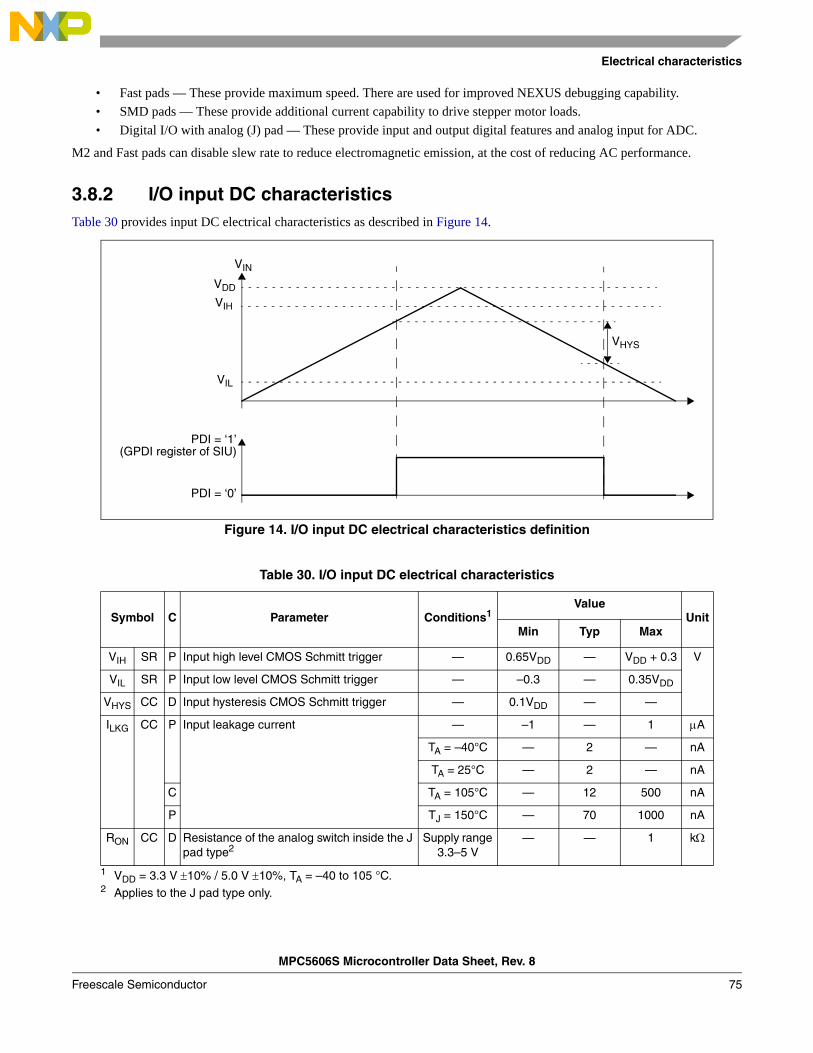
Electrical characteristics
MPC5606S Microcontroller Data Sheet, Rev. 8
Freescale Semiconductor 75
• Fast pads — These provide maximum speed. There are used for improved NEXUS debugging capability.
• SMD pads — These provide additional current capability to drive stepper motor loads.
• Digital I/O with analog (J) pad — These provide input and output digital features and analog input for ADC.
M2 and Fast pads can disable slew rate to reduce electromagnetic emission, at the cost of reducing AC performance.
3.8.2 I/O input DC characteristicsTable 30 provides input DC electrical characteristics as described in Figure 14.
Figure 14. I/O input DC electrical characteristics definition
Table 30. I/O input DC electrical characteristics
Symbol C Parameter Conditions1
1 VDD = 3.3 V 10% / 5.0 V 10%, TA = –40 to 105 °C.
ValueUnit
Min Typ Max
VIH SR P Input high level CMOS Schmitt trigger — 0.65VDD — VDD + 0.3 V
VIL SR P Input low level CMOS Schmitt trigger — –0.3 — 0.35VDD
VHYS CC D Input hysteresis CMOS Schmitt trigger — 0.1VDD — —
ILKG CC P Input leakage current — –1 — 1 A
TA = –40°C — 2 — nA
TA = 25°C — 2 — nA
C TA = 105°C — 12 500 nA
P TJ = 150°C — 70 1000 nA
RON CC D Resistance of the analog switch inside the J pad type2
2 Applies to the J pad type only.
Supply range 3.3–5 V
— — 1 k
VIL
VIN
VIH
PDI = ‘1’
VDD
VHYS
(GPDI register of SIU)
PDI = ‘0’
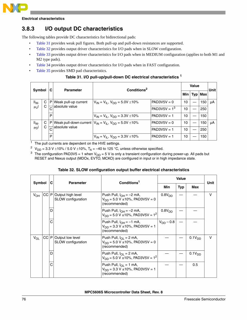
MPC5606S Microcontroller Data Sheet, Rev. 8
Electrical characteristics
Freescale Semiconductor76
3.8.3 I/O output DC characteristicsThe following tables provide DC characteristics for bidirectional pads:
• Table 31 provides weak pull figures. Both pull-up and pull-down resistances are supported.
• Table 32 provides output driver characteristics for I/O pads when in SLOW configuration.
• Table 33 provides output driver characteristics for I/O pads when in MEDIUM configuration (applies to both M1 and M2 type pads).
• Table 34 provides output driver characteristics for I/O pads when in FAST configuration.
• Table 35 provides SMD pad characteristics.
Table 31. I/O pull-up/pull-down DC electrical characteristics 1
1 The pull currents are dependent on the HVE settings.
Symbol C Parameter Conditions2
2 VDD = 3.3 V 10% / 5.0 V 10%, TA = –40 to 125 °C, unless otherwise specified.
ValueUnit
Min Typ Max
|IW-
PU|CC
P Weak pull-up current absolute value
VIN = VIL, VDD = 5.0V 10% PAD3V5V = 0 10 — 150 µA
C PAD3V5V = 13
3 The configuration PAD3V5 = 1 when VDD = 5 V is only a transient configuration during power-up. All pads but RESET and Nexus output (MDOx, EVTO, MCKO) are configured in input or in high impedance state.
10 — 250
P VIN = VIL, VDD = 3.3V 10% PAD3V5V = 1 10 — 150
|IW-
PD|CC
P Weak pull-down current absolute value
VIN = VIL, VDD = 5.0V 10% PAD3V5V = 0 10 — 150 µA
C PAD3V5V = 1 10 — 250
P VIN = VIL, VDD = 3.3V 10% PAD3V5V = 1 10 — 150
Table 32. SLOW configuration output buffer electrical characteristics
Symbol C Parameter Conditions1Value
UnitMin Typ Max
VOH CC P Output high levelSLOW configuration
Push Pull, IOH = –2 mA,VDD = 5.0 V ±10%, PAD3V5V = 0(recommended)
0.8VDD — — V
D Push Pull, IOH = –2 mA,VDD = 5.0 V ±10%, PAD3V5V = 12
0.8VDD — —
C Push Pull, IOH = –1 mA,VDD = 3.3 V ±10%, PAD3V5V = 1(recommended)
VDD – 0.8 — —
VOL CC P Output low levelSLOW configuration
Push Pull, IOL = 2 mA,VDD = 5.0 V ±10%, PAD3V5V = 0(recommended)
— — 0.1VDD V
D Push Pull, IOL = 2 mA,VDD = 5.0 V ±10%, PAD3V5V = 12
— — 0.1VDD
C Push Pull, IOL = 1 mA,VDD = 3.3 V ±10%, PAD3V5V = 1(recommended)
— — 0.5
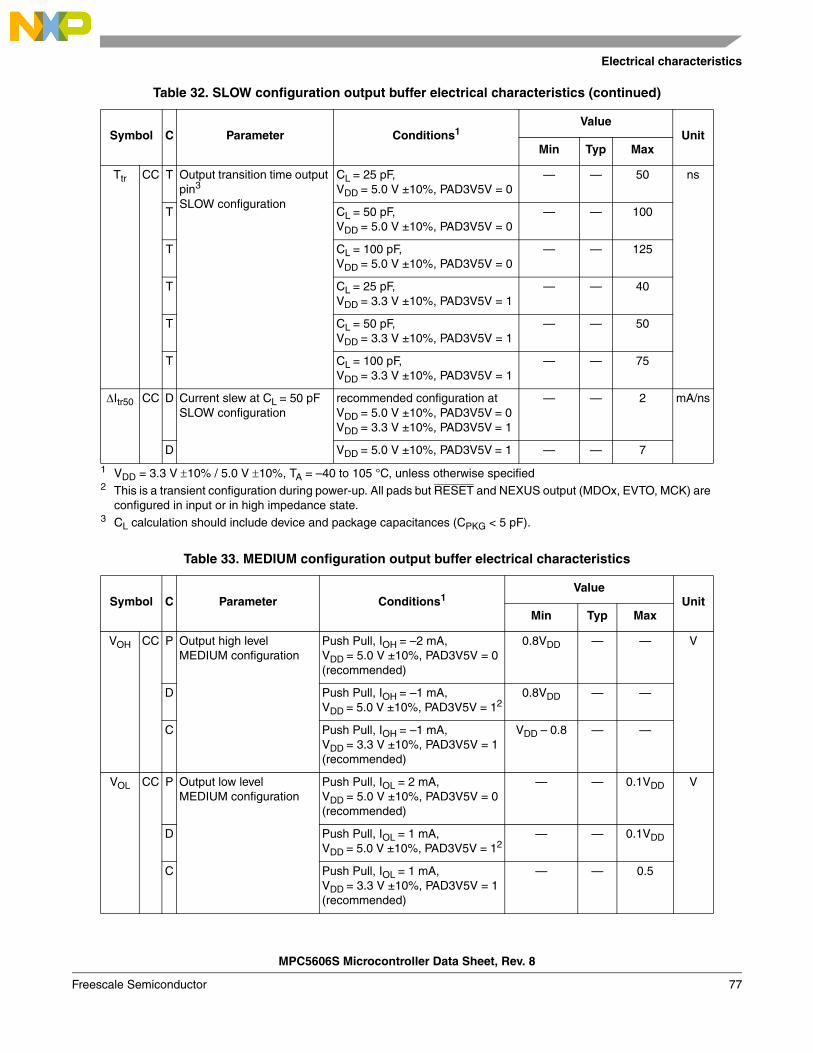
Electrical characteristics
MPC5606S Microcontroller Data Sheet, Rev. 8
Freescale Semiconductor 77
Ttr CC T Output transition time output pin3
SLOW configuration
CL = 25 pF,VDD = 5.0 V ±10%, PAD3V5V = 0
— — 50 ns
T CL = 50 pF,VDD = 5.0 V ±10%, PAD3V5V = 0
— — 100
T CL = 100 pF,VDD = 5.0 V ±10%, PAD3V5V = 0
— — 125
T CL = 25 pF,VDD = 3.3 V ±10%, PAD3V5V = 1
— — 40
T CL = 50 pF,VDD = 3.3 V ±10%, PAD3V5V = 1
— — 50
T CL = 100 pF,VDD = 3.3 V ±10%, PAD3V5V = 1
— — 75
Itr50 CC D Current slew at CL = 50 pFSLOW configuration
recommended configuration atVDD = 5.0 V ±10%, PAD3V5V = 0VDD = 3.3 V ±10%, PAD3V5V = 1
— — 2 mA/ns
D VDD = 5.0 V ±10%, PAD3V5V = 1 — — 7
1 VDD = 3.3 V 10% / 5.0 V 10%, TA = –40 to 105 °C, unless otherwise specified2 This is a transient configuration during power-up. All pads but RESET and NEXUS output (MDOx, EVTO, MCK) are
configured in input or in high impedance state.3 CL calculation should include device and package capacitances (CPKG < 5 pF).
Table 33. MEDIUM configuration output buffer electrical characteristics
Symbol C Parameter Conditions1Value
UnitMin Typ Max
VOH CC P Output high levelMEDIUM configuration
Push Pull, IOH = –2 mA,VDD = 5.0 V ±10%, PAD3V5V = 0(recommended)
0.8VDD — — V
D Push Pull, IOH = –1 mA,VDD = 5.0 V ±10%, PAD3V5V = 12
0.8VDD — —
C Push Pull, IOH = –1 mA,VDD = 3.3 V ±10%, PAD3V5V = 1(recommended)
VDD – 0.8 — —
VOL CC P Output low levelMEDIUM configuration
Push Pull, IOL = 2 mA,VDD = 5.0 V ±10%, PAD3V5V = 0(recommended)
— — 0.1VDD V
D Push Pull, IOL = 1 mA,VDD = 5.0 V ±10%, PAD3V5V = 12
— — 0.1VDD
C Push Pull, IOL = 1 mA,VDD = 3.3 V ±10%, PAD3V5V = 1(recommended)
— — 0.5
Table 32. SLOW configuration output buffer electrical characteristics (continued)
Symbol C Parameter Conditions1Value
UnitMin Typ Max
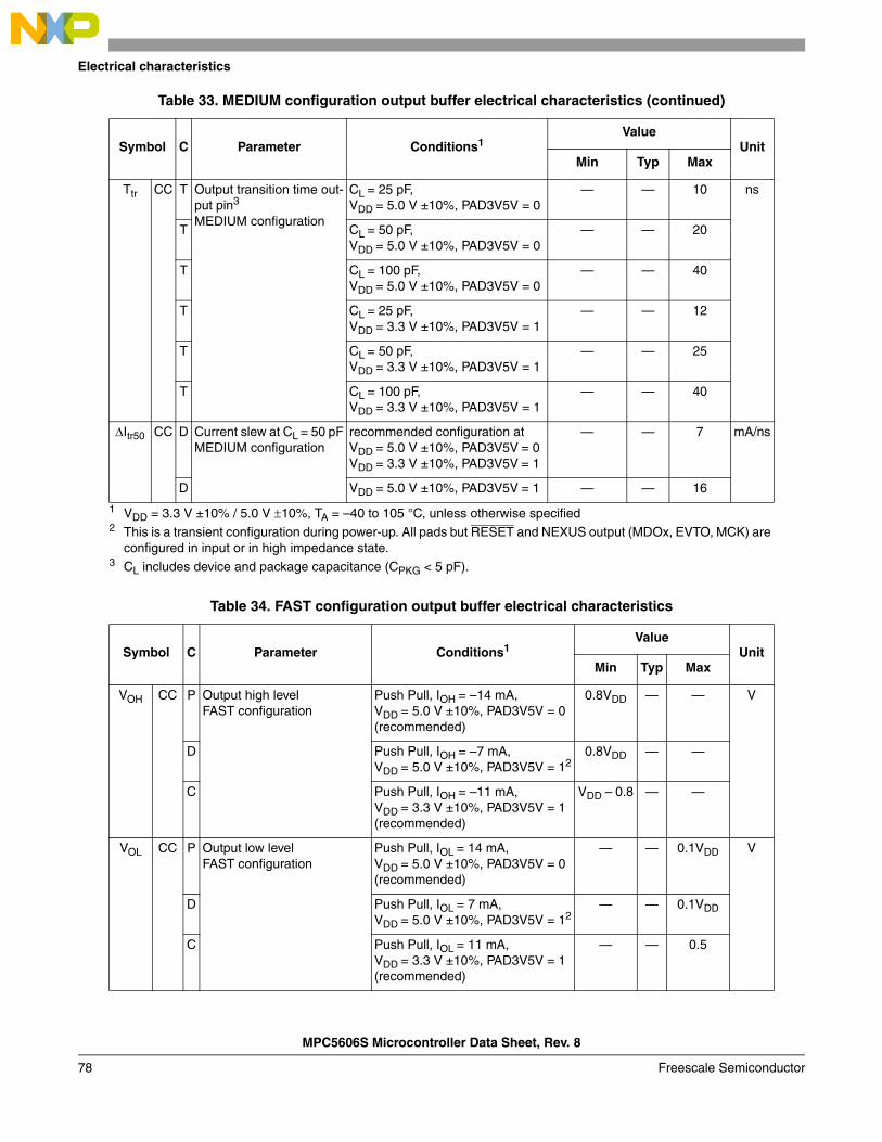
MPC5606S Microcontroller Data Sheet, Rev. 8
Electrical characteristics
Freescale Semiconductor78
Ttr CC T Output transition time out-put pin3
MEDIUM configuration
CL = 25 pF, VDD = 5.0 V ±10%, PAD3V5V = 0
— — 10 ns
T CL = 50 pF, VDD = 5.0 V ±10%, PAD3V5V = 0
— — 20
T CL = 100 pF, VDD = 5.0 V ±10%, PAD3V5V = 0
— — 40
T CL = 25 pF, VDD = 3.3 V ±10%, PAD3V5V = 1
— — 12
T CL = 50 pF, VDD = 3.3 V ±10%, PAD3V5V = 1
— — 25
T CL = 100 pF, VDD = 3.3 V ±10%, PAD3V5V = 1
— — 40
Itr50 CC D Current slew at CL = 50 pFMEDIUM configuration
recommended configuration atVDD = 5.0 V ±10%, PAD3V5V = 0VDD = 3.3 V ±10%, PAD3V5V = 1
— — 7 mA/ns
D VDD = 5.0 V ±10%, PAD3V5V = 1 — — 16
1 VDD = 3.3 V ±10% / 5.0 V 10%, TA = –40 to 105 °C, unless otherwise specified2 This is a transient configuration during power-up. All pads but RESET and NEXUS output (MDOx, EVTO, MCK) are
configured in input or in high impedance state.3 CL includes device and package capacitance (CPKG < 5 pF).
Table 34. FAST configuration output buffer electrical characteristics
Symbol C Parameter Conditions1Value
UnitMin Typ Max
VOH CC P Output high levelFAST configuration
Push Pull, IOH = –14 mA,VDD = 5.0 V ±10%, PAD3V5V = 0(recommended)
0.8VDD — — V
D Push Pull, IOH = –7 mA,VDD = 5.0 V ±10%, PAD3V5V = 12
0.8VDD — —
C Push Pull, IOH = –11 mA,VDD = 3.3 V ±10%, PAD3V5V = 1(recommended)
VDD – 0.8 — —
VOL CC P Output low levelFAST configuration
Push Pull, IOL = 14 mA,VDD = 5.0 V ±10%, PAD3V5V = 0(recommended)
— — 0.1VDD V
D Push Pull, IOL = 7 mA,VDD = 5.0 V ±10%, PAD3V5V = 12
— — 0.1VDD
C Push Pull, IOL = 11 mA,VDD = 3.3 V ±10%, PAD3V5V = 1(recommended)
— — 0.5
Table 33. MEDIUM configuration output buffer electrical characteristics (continued)
Symbol C Parameter Conditions1Value
UnitMin Typ Max
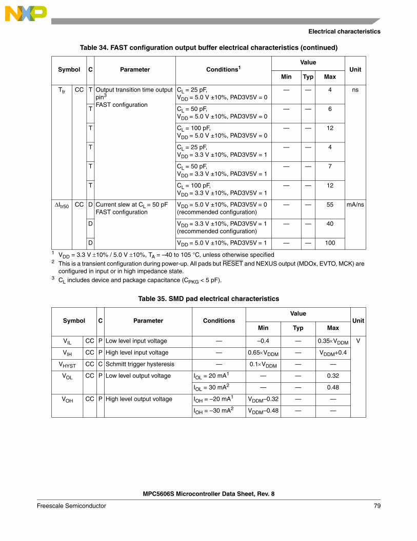
Electrical characteristics
MPC5606S Microcontroller Data Sheet, Rev. 8
Freescale Semiconductor 79
Ttr CC T Output transition time output pin3
FAST configuration
CL = 25 pF,VDD = 5.0 V ±10%, PAD3V5V = 0
— — 4 ns
T CL = 50 pF,VDD = 5.0 V ±10%, PAD3V5V = 0
— — 6
T CL = 100 pF,VDD = 5.0 V ±10%, PAD3V5V = 0
— — 12
T CL = 25 pF,VDD = 3.3 V ±10%, PAD3V5V = 1
— — 4
T CL = 50 pF,VDD = 3.3 V ±10%, PAD3V5V = 1
— — 7
T CL = 100 pF,VDD = 3.3 V ±10%, PAD3V5V = 1
— — 12
Itr50 CC D Current slew at CL = 50 pFFAST configuration
VDD = 5.0 V ±10%, PAD3V5V = 0(recommended configuration)
— — 55 mA/ns
D VDD = 3.3 V ±10%, PAD3V5V = 1(recommended configuration)
— — 40
D VDD = 5.0 V ±10%, PAD3V5V = 1 — — 100
1 VDD = 3.3 V 10% / 5.0 V 10%, TA = –40 to 105 °C, unless otherwise specified2 This is a transient configuration during power-up. All pads but RESET and NEXUS output (MDOx, EVTO, MCK) are
configured in input or in high impedance state.3 CL includes device and package capacitance (CPKG < 5 pF).
Table 35. SMD pad electrical characteristics
Symbol C Parameter ConditionsValue
UnitMin Typ Max
VIL CC P Low level input voltage — –0.4 — 0.35VDDM V
VIH CC P High level input voltage — 0.65VDDM — VDDM+0.4
VHYST CC C Schmitt trigger hysteresis — 0.1VDDM — —
VOL CC P Low level output voltage IOL = 20 mA1 — — 0.32
IOL = 30 mA2 — — 0.48
VOH CC P High level output voltage IOH = –20 mA1 VDDM–0.32 — —
IOH = –30 mA2 VDDM–0.48 — —
Table 34. FAST configuration output buffer electrical characteristics (continued)
Symbol C Parameter Conditions1Value
UnitMin Typ Max
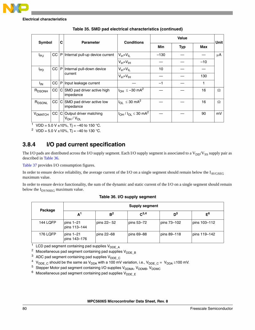
MPC5606S Microcontroller Data Sheet, Rev. 8
Electrical characteristics
Freescale Semiconductor80
3.8.4 I/O pad current specificationThe I/O pads are distributed across the I/O supply segment. Each I/O supply segment is associated to a VDD/VSS supply pair as described in Table 36.
Table 37 provides I/O consumption figures.
In order to ensure device reliability, the average current of the I/O on a single segment should remain below the IAVGSEG maximum value.
In order to ensure device functionality, the sum of the dynamic and static current of the I/O on a single segment should remain below the IDYNSEG maximum value.
IPU CC P Internal pull-up device current Vin=VIL –130 — — A
Vin=VIH — — –10
IPD CC P Internal pull-down device current
Vin=VIL 10 — —
Vin=VIH — — 130
IIN CC P Input leakage current — –1 — 1
RDSONH CC C SMD pad driver active high impedance
IOH –30 mA2 — — 16
RDSONL CC C SMD pad driver active low impedance
IOL 30 mA2 — — 16
VOMATCH CC C Output driver matching VOH / VOL
IOH / IOL 30 mA2 — — 90 mV
1 VDD = 5.0 V ±10%, Tj = –40 to 150 °C.2 VDD = 5.0 V ±10%, Tj = –40 to 130 °C.
Table 36. I/O supply segment
PackageSupply segment
A1
1 LCD pad segment containing pad supplies VDDE_A
B2
2 Miscellaneous pad segment containing pad supplies VDDE_B
C3,4
3 ADC pad segment containing pad supplies VDDE_C4 VDDE_C should be the same as VDDA with a 100 mV variation, i.e., VDDE_C = VDDA 100 mV.
D5
5 Stepper Motor pad segment containing I/O supplies VDDMA, VDDMB, VDDMC
E6
6 Miscellaneous pad segment containing pad supplies VDDE_E
144 LQFP pins 1–21pins 113–144
pins 22– 52 pins 53–72 pins 73–102 pins 103–112
176 LQFP pins 1–21pins 143–176
pins 22–68 pins 69–88 pins 89–118 pins 119–142
Table 35. SMD pad electrical characteristics (continued)
Symbol C Parameter ConditionsValue
UnitMin Typ Max
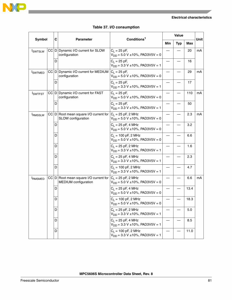
Electrical characteristics
MPC5606S Microcontroller Data Sheet, Rev. 8
Freescale Semiconductor 81
Table 37. I/O consumption
Symbol C Parameter Conditions1Value
UnitMin Typ Max
ISWTSLW CC D Dynamic I/O current for SLOW configuration
CL = 25 pF,VDD = 5.0 V ±10%, PAD3V5V = 0
— — 20 mA
D CL = 25 pF,VDD = 3.3 V ±10%, PAD3V5V = 1
— — 16
ISWTMED CC D Dynamic I/O current for MEDIUM configuration
CL = 25 pF,VDD = 5.0 V ±10%, PAD3V5V = 0
— — 29 mA
D CL = 25 pF,VDD = 3.3 V ±10%, PAD3V5V = 1
— — 17
ISWTFST CC D Dynamic I/O current for FAST configuration
CL = 25 pF,VDD = 5.0 V ±10%, PAD3V5V = 0
— — 110 mA
D CL = 25 pF,VDD = 3.3 V ±10%, PAD3V5V = 1
— — 50
IRMSSLW CC D Root mean square I/O current for SLOW configuration
CL = 25 pF, 2 MHzVDD = 5.0 V ±10%, PAD3V5V = 0
— — 2.3 mA
D CL = 25 pF, 4 MHzVDD = 5.0 V ±10%, PAD3V5V = 0
— — 3.2
D CL = 100 pF, 2 MHzVDD = 5.0 V ±10%, PAD3V5V = 0
— — 6.6
D CL = 25 pF, 2 MHzVDD = 3.3 V ±10%, PAD3V5V = 1
— — 1.6
D CL = 25 pF, 4 MHzVDD = 3.3 V ±10%, PAD3V5V = 1
— — 2.3
D CL = 100 pF, 2 MHzVDD = 3.3 V ±10%, PAD3V5V = 1
— — 4.7
IRMSMED CC D Root mean square I/O current for MEDIUM configuration
CL = 25 pF, 2 MHzVDD = 5.0 V ±10%, PAD3V5V = 0
— — 6.6 mA
D CL = 25 pF, 4 MHzVDD = 5.0 V ±10%, PAD3V5V = 0
— — 13.4
D CL = 100 pF, 2 MHzVDD = 5.0 V ±10%, PAD3V5V = 0
— — 18.3
D CL = 25 pF, 2 MHzVDD = 3.3 V ±10%, PAD3V5V = 1
— — 5.0
D CL = 25 pF, 4 MHzVDD = 3.3 V ±10%, PAD3V5V = 1
— — 8.5
D CL = 100 pF, 2 MHzVDD = 3.3 V ±10%, PAD3V5V = 1
— — 11.0
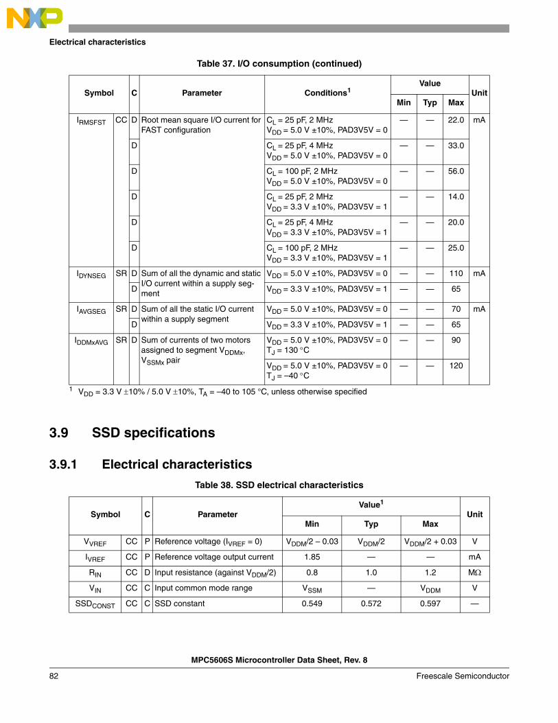
MPC5606S Microcontroller Data Sheet, Rev. 8
Electrical characteristics
Freescale Semiconductor82
3.9 SSD specifications
3.9.1 Electrical characteristics
IRMSFST CC D Root mean square I/O current for FAST configuration
CL = 25 pF, 2 MHzVDD = 5.0 V ±10%, PAD3V5V = 0
— — 22.0 mA
D CL = 25 pF, 4 MHzVDD = 5.0 V ±10%, PAD3V5V = 0
— — 33.0
D CL = 100 pF, 2 MHzVDD = 5.0 V ±10%, PAD3V5V = 0
— — 56.0
D CL = 25 pF, 2 MHzVDD = 3.3 V ±10%, PAD3V5V = 1
— — 14.0
D CL = 25 pF, 4 MHzVDD = 3.3 V ±10%, PAD3V5V = 1
— — 20.0
D CL = 100 pF, 2 MHzVDD = 3.3 V ±10%, PAD3V5V = 1
— — 25.0
IDYNSEG SR D Sum of all the dynamic and static I/O current within a supply seg-ment
VDD = 5.0 V ±10%, PAD3V5V = 0 — — 110 mA
D VDD = 3.3 V ±10%, PAD3V5V = 1 — — 65
IAVGSEG SR D Sum of all the static I/O current within a supply segment
VDD = 5.0 V ±10%, PAD3V5V = 0 — — 70 mA
D VDD = 3.3 V ±10%, PAD3V5V = 1 — — 65
IDDMxAVG SR D Sum of currents of two motors assigned to segment VDDMx, VSSMx pair
VDD = 5.0 V ±10%, PAD3V5V = 0TJ = 130 C
— — 90
VDD = 5.0 V ±10%, PAD3V5V = 0TJ = –40 C
— — 120
1 VDD = 3.3 V 10% / 5.0 V 10%, TA = –40 to 105 °C, unless otherwise specified
Table 38. SSD electrical characteristics
Symbol C ParameterValue1
UnitMin Typ Max
VVREF CC P Reference voltage (IVREF = 0) VDDM/2 – 0.03 VDDM/2 VDDM/2 + 0.03 V
IVREF CC P Reference voltage output current 1.85 — — mA
RIN CC D Input resistance (against VDDM/2) 0.8 1.0 1.2 M
VIN CC C Input common mode range VSSM — VDDM V
SSDCONST CC C SSD constant 0.549 0.572 0.597 —
Table 37. I/O consumption (continued)
Symbol C Parameter Conditions1Value
UnitMin Typ Max
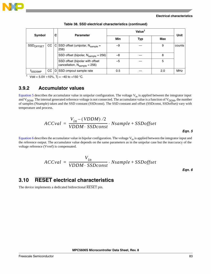
Electrical characteristics
MPC5606S Microcontroller Data Sheet, Rev. 8
Freescale Semiconductor 83
3.9.2 Accumulator valuesEquation 5 describes the accumulator value in unipolar configuration. The voltage Vin is applied between the integrator input and VDDM. The internal generated reference voltage is not connected. The accumulator value is a function of VDDM, the number of samples (Nsample) taken and the SSD constant (SSDconst). The SSD constant and offset (SSDconst, SSDoffset) vary with temperature and process.
Eqn. 5
Equation 6 describes the accumulator value in bipolar configuration. The voltage Vin is applied between the integrator input and the reference output. The accumulator value depends on the same parameters as in the unipolar case but the inaccuracy of the voltage reference (Vvref) is compensated.
Eqn. 6
3.10 RESET electrical characteristicsThe device implements a dedicated bidirectional RESET pin.
SSDOFFSET CC C SSD offset (unipolar, Nsample = 256)
–9 — 9 counts
SSD offset (bipolar, Nsample = 256) –8 — 8
SSD offset (bipolar with offset cancellation, Nsample = 256)
–5 — 5
fSSDSMP CC D SSD cmpout sample rate 0.5 — 2.0 MHz
1 Vdd = 5.0V 10%, Tj = –40 to +150 °C.
Table 38. SSD electrical characteristics (continued)
Symbol C ParameterValue1
UnitMin Typ Max
ACCvalVin VDDM 2–
VDDM SSDconst------------------------------------------------ Nsample SSDoffset+=
ACCvalVin
VDDM SSDconst------------------------------------------------ Nsample SSDoffset+=
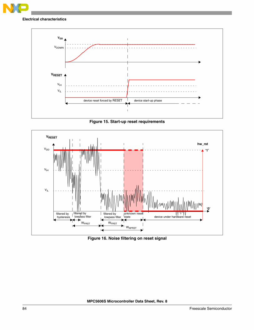
MPC5606S Microcontroller Data Sheet, Rev. 8
Electrical characteristics
Freescale Semiconductor84
Figure 15. Start-up reset requirements
Figure 16. Noise filtering on reset signal
VIL
VDD
device reset forced by RESET
VDDMIN
VIH
device start-up phase
VRESET
VRESET
VIL
VIH
VDD
filtered by hysteresis
filtered by lowpass filter
WFRST
WNFRST
hw_rst
‘1’
‘0’filtered by lowpass filter
WFRST
unknown resetstate device under hardware reset
Electrical characteristics
MPC5606S Microcontroller Data Sheet, Rev. 8
Freescale Semiconductor 85
Table 39. Reset electrical characteristics
Symbol C Parameter Conditions1
1 VDD = 3.3 V ±10% / 5.0 V ±10%, TA = –40 to 105 °C, unless otherwise specified
ValueUnit
Min Typ Max
VIH SR P Input high level CMOS Schmitt Trigger
— 0.65VDD — VDD + 0.4 V
VIL SR P Input low level CMOS Schmitt Trigger
— –0.4 — 0.35VDD V
VHYS CC D Input hysteresis CMOS Schmitt Trigger
— 0.1VDD — — V
VOL CC P Output low level Push Pull, IOL = 2 mA,VDD = 5.0 V ±10%, PAD3V5V = 0(recommended)
— — 0.1VDD V
D Push Pull, IOL = 1 mA,VDD = 5.0 V ±10%, PAD3V5V = 12
2 This is a transient configuration during power-up, up to the end of reset PHASE2 (refer to reset generation module (RGM) section of the device reference manual).
— — 0.1VDD
C Push Pull, IOL = 1 mA,VDD = 3.3 V ±10%, PAD3V5V = 1 (recommended)
— — 0.5
Ttr CC T Output transition time output pin3
MEDIUM configuration
3 CL includes device and package capacitance (CPKG < 5 pF).
CL = 25 pF,VDD = 5.0 V ±10%, PAD3V5V = 0
— — 10 ns
T CL = 50 pF,VDD = 5.0 V ±10%, PAD3V5V = 0
— — 20
T CL = 100 pF,VDD = 5.0 V ±10%, PAD3V5V = 0
— — 40
T CL = 25 pF,VDD = 3.3 V ±10%, PAD3V5V = 1
— — 12
T CL = 50 pF,VDD = 3.3 V ±10%, PAD3V5V = 1
— — 25
T CL = 100 pF,VDD = 3.3 V ±10%, PAD3V5V = 1
— — 40
WFRST SR P RESET input filtered pulse — — — 40 ns
WNFRST SR P RESET input not filtered pulse — 1000 — — ns
IWPU CC P Weak pull-up current absolute value
— 10 — 150 µA
D RUN Current during RESET Before Flash is ready — 10 — mA
After Flash is ready — 20 — mA
MPC5606S Microcontroller Data Sheet, Rev. 8
Electrical characteristics
Freescale Semiconductor86
3.11 Fast external crystal oscillator (4–16 MHz) electrical characteristics
The device provides an oscillator/resonator driver. Figure 17 describes a simple model of the internal oscillator driver and provides an example of a connection for an oscillator or a resonator.
Figure 17. Crystal oscillator and resonator connection scheme
NOTEXTAL/EXTAL must not be directly used to drive external circuits.
Table 40. Crystal description
Nominalfrequency
(MHz)
NDK crystal reference
Crystalequivalent
seriesresistance
ESR
Crystalmotional
capacitance(Cm) fF
Crystalmotional
inductance(Lm) mH
Load onxtalin/xtalout
C1 = C2(pF)1
Shuntcapacitance
between xtalout
and xtalinC02 (pF)
4 NX8045GB 300 2.68 591.0 21 2.93
8 NX5032GA 300 2.46 160.7 17 3.01
10 150 2.93 86.6 15 2.91
12 120 3.11 56.5 15 2.93
16 120 3.90 25.3 10 3.00
CL
CL
Cry
stal
EXTAL
XTAL
Res
on
ato
r
EXTAL
XTAL
DEVICE
DEVICE
DEVICEEXTAL
XTAL
I
R
VDD
Electrical characteristics
MPC5606S Microcontroller Data Sheet, Rev. 8
Freescale Semiconductor 87
Figure 18. Fast external crystal oscillator (4–16 MHz) electrical characteristics
1 The values specified for C1 and C2 are the same as used in simulations. It should be ensured that the testing includes all the parasitics (from the board, probe, crystal, etc.) as the AC / transient behavior depends upon them.
2 The value of C0 specified here includes 2 pF additional capacitance for parasitics (to be seen with bond-pads, package, etc.).
Table 41. Resonator description
CSTCR4M00G53-R0 CSTCR4M00G55-R0
Vibration Fundamental
Fr (kHz) 3929.50 3898.00
Fa (kHz) 4163.25 4123.00
Fa–Fr (dF) (kHz) 233.75 225.00
Ra (k) 372.41 465.03
R1 () 12.78 11.38
L1 (mH) 0.84443 0.88244
C1 (pF) 1.94268 1.88917
Co (pF) 15.85730 15.90537
Qm 1630.93 1899.77
CL1 (nominal) (pF) 15 39
CL2 (nominal) (pF) 15 39
VFXOSCOP
tFXOSCSU
VXTAL
VFXOSC
valid internal clock
90%
10%
1/fFXOSC
S_MTRANS bit (ME_GS register)
‘1’
‘0’
MPC5606S Microcontroller Data Sheet, Rev. 8
Electrical characteristics
Freescale Semiconductor88
3.12 Slow external crystal oscillator (32 KHz) electrical characteristicsThe device provides a low power oscillator/resonator driver.
Table 42. Fast external crystal oscillator (4–16 MHz) electrical characteristics
Symbol C Parameter Conditions1
1 VDD = 3.3 V ±10% / 5.0 V ±10%, TA = –40 to 105 °C, unless otherwise specified
ValueUnit
Min Typ Max
fFXOSC SR — Fast external crystal oscillator frequency
— 4.0 — 16.0 MHz
gmFXOSC CC C Fast external crystal oscillator transconductance
VDD = 3.3 V ±10%,PAD3V5V = 1OSCILLATOR_MARGIN = 0
2.2 — 8.2 mA/V
CC P VDD = 5.0 V ±10%,PAD3V5V = 0OSCILLATOR_MARGIN = 0
2.0 — 7.4
CC C VDD = 3.3 V ±10%,PAD3V5V = 1OSCILLATOR_MARGIN = 1
2.7 — 9.7
CC C VDD = 5.0 V ±10%,PAD3V5V = 0OSCILLATOR_MARGIN = 1
2.5 — 9.2
VFXOSC CC T Oscillation amplitude at EXTAL
fOSC = 4 MHz,OSCILLATOR_MARGIN = 0
1.3 — — V
fOSC = 16 MHz,OSCILLATOR_MARGIN = 1
1.3 — —
VFXOSCOP CC C Oscillation operating point — — 0.95 — V
IFXOSC,2
2 Stated values take into account only analog module consumption but not the digital contributor (clock tree and enabled peripherals)
CC T Fast external crystal oscillator consumption
— — 2 3 mA
TFXOSCSU CC T Fast external crystal oscillator start-up time
fOSC = 4 MHz,OSCILLATOR_MARGIN = 0
— — 6 ms
fOSC = 16 MHz,OSCILLATOR_MARGIN = 1
— — 1.8
VIH SR P Input high level CMOS(Schmitt Trigger)
Oscillator bypass mode 0.65 VDD — VDD + 0.4 V
VIL SR P Input low level CMOS(Schmitt Trigger)
Oscillator bypass mode –0.4 — 0.35 VDD V
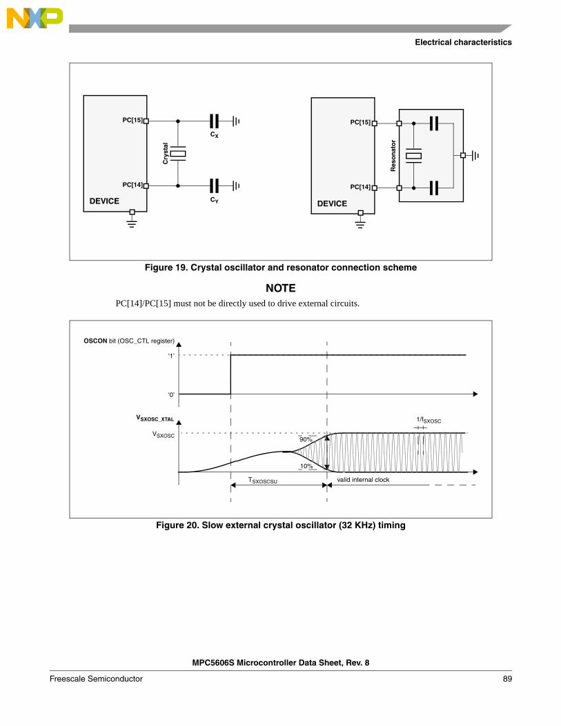
Electrical characteristics
MPC5606S Microcontroller Data Sheet, Rev. 8
Freescale Semiconductor 89
Figure 19. Crystal oscillator and resonator connection scheme
NOTEPC[14]/PC[15] must not be directly used to drive external circuits.
Figure 20. Slow external crystal oscillator (32 KHz) timing
CY
CX
Cry
stal
PC[14]
PC[15]
Res
on
ato
r
PC[14]
PC[15]
DEVICE DEVICE
OSCON bit (OSC_CTL register)
TSXOSCSU
‘1’
VSXOSC_XTAL
VSXOSC
valid internal clock
90%
10%
1/fSXOSC
‘0’
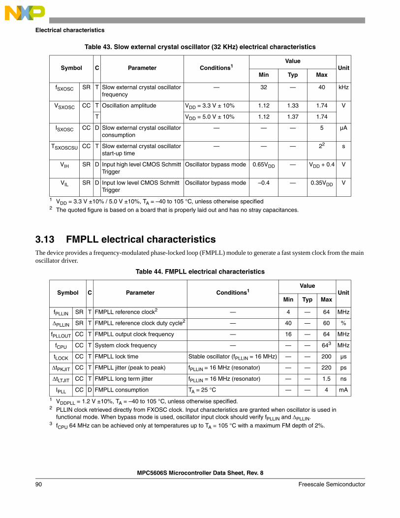
MPC5606S Microcontroller Data Sheet, Rev. 8
Electrical characteristics
Freescale Semiconductor90
3.13 FMPLL electrical characteristicsThe device provides a frequency-modulated phase-locked loop (FMPLL) module to generate a fast system clock from the main oscillator driver.
Table 43. Slow external crystal oscillator (32 KHz) electrical characteristics
Symbol C Parameter Conditions1
1 VDD = 3.3 V ±10% / 5.0 V ±10%, TA = –40 to 105 °C, unless otherwise specified
ValueUnit
Min Typ Max
fSXOSC SR T Slow external crystal oscillator frequency
— 32 — 40 kHz
VSXOSC CC T Oscillation amplitude VDD = 3.3 V ± 10% 1.12 1.33 1.74 V
T VDD = 5.0 V ± 10% 1.12 1.37 1.74
ISXOSC CC D Slow external crystal oscillator consumption
— — — 5 µA
TSXOSCSU CC T Slow external crystal oscillator start-up time
— — — 22
2 The quoted figure is based on a board that is properly laid out and has no stray capacitances.
s
VIH SR D Input high level CMOS Schmitt Trigger
Oscillator bypass mode 0.65VDD — VDD + 0.4 V
VIL SR D Input low level CMOS Schmitt Trigger
Oscillator bypass mode –0.4 — 0.35VDD V
Table 44. FMPLL electrical characteristics
Symbol C Parameter Conditions1
1 VDDPLL = 1.2 V ±10%, TA = –40 to 105 °C, unless otherwise specified.
ValueUnit
Min Typ Max
fPLLIN SR T FMPLL reference clock2
2 PLLIN clock retrieved directly from FXOSC clock. Input characteristics are granted when oscillator is used in functional mode. When bypass mode is used, oscillator input clock should verify fPLLIN and PLLIN.
— 4 — 64 MHz
PLLIN SR T FMPLL reference clock duty cycle2 — 40 — 60 %
fPLLOUT CC T FMPLL output clock frequency — 16 — 64 MHz
fCPU CC T System clock frequency — — — 643
3 fCPU 64 MHz can be achieved only at temperatures up to TA = 105 °C with a maximum FM depth of 2%.
MHz
tLOCK CC T FMPLL lock time Stable oscillator (fPLLIN = 16 MHz) — — 200 µs
tPKJIT CC T FMPLL jitter (peak to peak) fPLLIN = 16 MHz (resonator) — — 220 ps
tLTJIT CC T FMPLL long term jitter fPLLIN = 16 MHz (resonator) — — 1.5 ns
IPLL CC D FMPLL consumption TA = 25 °C — — 4 mA
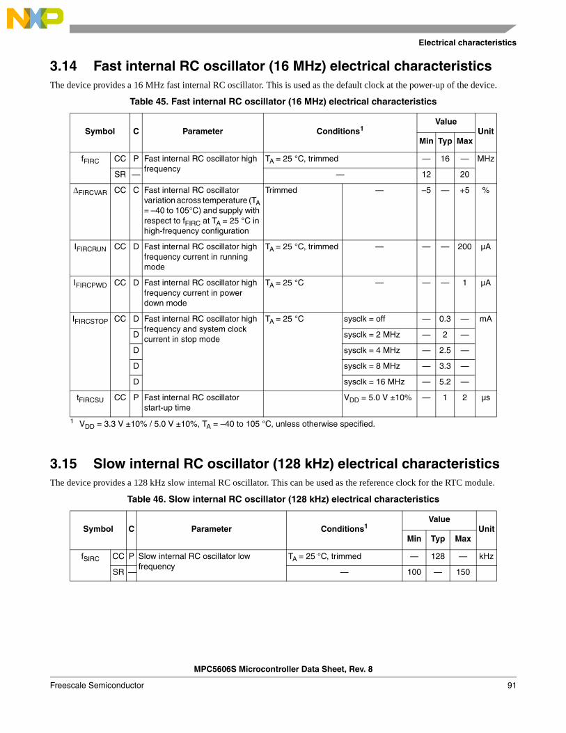
Electrical characteristics
MPC5606S Microcontroller Data Sheet, Rev. 8
Freescale Semiconductor 91
3.14 Fast internal RC oscillator (16 MHz) electrical characteristicsThe device provides a 16 MHz fast internal RC oscillator. This is used as the default clock at the power-up of the device.
3.15 Slow internal RC oscillator (128 kHz) electrical characteristicsThe device provides a 128 kHz slow internal RC oscillator. This can be used as the reference clock for the RTC module.
Table 45. Fast internal RC oscillator (16 MHz) electrical characteristics
Symbol C Parameter Conditions1
1 VDD = 3.3 V ±10% / 5.0 V ±10%, TA = –40 to 105 °C, unless otherwise specified.
ValueUnit
Min Typ Max
fFIRC CC P Fast internal RC oscillator high frequency
TA = 25 °C, trimmed — 16 — MHz
SR — — 12 20
FIRCVAR CC C Fast internal RC oscillator variation across temperature (TA = –40 to 105°C) and supply with respect to fFIRC at TA = 25 °C in high-frequency configuration
Trimmed — –5 — +5 %
IFIRCRUN CC D Fast internal RC oscillator high frequency current in running mode
TA = 25 °C, trimmed — — — 200 µA
IFIRCPWD CC D Fast internal RC oscillator high frequency current in power down mode
TA = 25 °C — — — 1 µA
IFIRCSTOP CC D Fast internal RC oscillator high frequency and system clock current in stop mode
TA = 25 °C sysclk = off — 0.3 — mA
D sysclk = 2 MHz — 2 —
D sysclk = 4 MHz — 2.5 —
D sysclk = 8 MHz — 3.3 —
D sysclk = 16 MHz — 5.2 —
tFIRCSU CC P Fast internal RC oscillator start-up time
VDD = 5.0 V ±10% — 1 2 µs
Table 46. Slow internal RC oscillator (128 kHz) electrical characteristics
Symbol C Parameter Conditions1Value
UnitMin Typ Max
fSIRC CC P Slow internal RC oscillator low frequency
TA = 25 °C, trimmed — 128 — kHz
SR — — 100 — 150
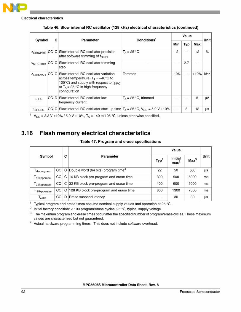
MPC5606S Microcontroller Data Sheet, Rev. 8
Electrical characteristics
Freescale Semiconductor92
3.16 Flash memory electrical characteristics
SIRCPRE CC C Slow internal RC oscillator precision after software trimming of fSIRC
TA = 25 °C 2 — +2 %
SIRCTRIM CC C Slow internal RC oscillator trimming step
— — 2.7 —
SIRCVAR CC C Slow internal RC oscillator variation across temperature (TA = –40°C to 105°C) and supply with respect to fSIRC at TA = 25 °C in high frequency configuration
Trimmed –10% — +10% kHz
ISIRC CC D Slow internal RC oscillator low frequency current
TA = 25 °C, trimmed — — 5 µA
tSIRCSU CC C Slow internal RC oscillator start-up time TA = 25 °C, VDD = 5.0 V ±10% — 8 12 µs
1 VDD = 3.3 V ±10% / 5.0 V ±10%, TA = –40 to 105 °C, unless otherwise specified.
Table 47. Program and erase specifications
Symbol C Parameter
Value
UnitTyp1
1 Typical program and erase times assume nominal supply values and operation at 25 °C.
Initial max2
2 Initial factory condition: < 100 program/erase cycles, 25 °C, typical supply voltage.
Max3
3 The maximum program and erase times occur after the specified number of program/erase cycles. These maximum values are characterized but not guaranteed.
Tdwprogram CC C Double word (64 bits) program time4
4 Actual hardware programming times. This does not include software overhead.
22 50 500 µs
T16kpperase CC C 16 KB block pre-program and erase time 300 500 5000 ms
T32kpperase CC C 32 KB block pre-program and erase time 400 600 5000 ms
T128kpperase CC C 128 KB block pre-program and erase time 800 1300 7500 ms
Teslat CC D Erase suspend latency — 30 30 µs
Table 46. Slow internal RC oscillator (128 kHz) electrical characteristics (continued)
Symbol C Parameter Conditions1Value
UnitMin Typ Max
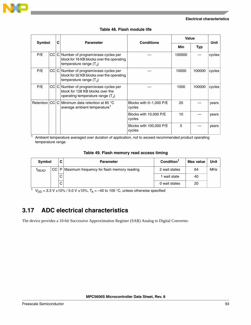
Electrical characteristics
MPC5606S Microcontroller Data Sheet, Rev. 8
Freescale Semiconductor 93
3.17 ADC electrical characteristics
The device provides a 10-bit Successive Approximation Register (SAR) Analog to Digital Converter.
Table 48. Flash module life
Symbol C Parameter ConditionsValue
UnitMin Typ
P/E CC C Number of program/erase cycles per block for 16 KB blocks over the operating temperature range (TJ)
— 100000 — cycles
P/E CC C Number of program/erase cycles per block for 32 KB blocks over the operating temperature range (TJ)
— 10000 100000 cycles
P/E CC C Number of program/erase cycles per block for 128 KB blocks over the operating temperature range (TJ)
— 1000 100000 cycles
Retention CC C Minimum data retention at 85 °C average ambient temperature1
1 Ambient temperature averaged over duration of application, not to exceed recommended product operating temperature range.
Blocks with 0–1,000 P/E cycles
20 — years
Blocks with 10,000 P/E cycles
10 — years
Blocks with 100,000 P/E cycles
5 — years
Table 49. Flash memory read access timing
Symbol C Parameter Condition1
1 VDD = 3.3 V ±10% / 5.0 V ±10%, TA = –40 to 105 C, unless otherwise specified
Max value Unit
fREAD CC P Maximum frequency for flash memory reading 2 wait states 64 MHz
C 1 wait state 40
C 0 wait states 20
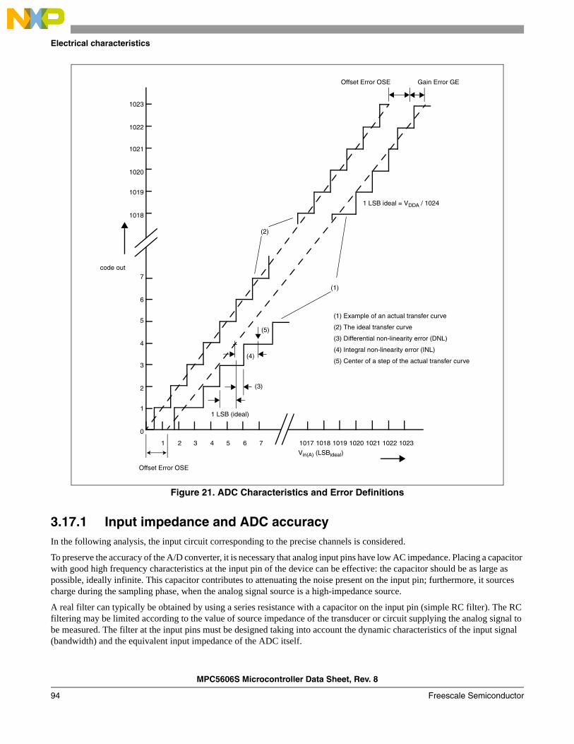
MPC5606S Microcontroller Data Sheet, Rev. 8
Electrical characteristics
Freescale Semiconductor94
Figure 21. ADC Characteristics and Error Definitions
3.17.1 Input impedance and ADC accuracyIn the following analysis, the input circuit corresponding to the precise channels is considered.
To preserve the accuracy of the A/D converter, it is necessary that analog input pins have low AC impedance. Placing a capacitor with good high frequency characteristics at the input pin of the device can be effective: the capacitor should be as large as possible, ideally infinite. This capacitor contributes to attenuating the noise present on the input pin; furthermore, it sources charge during the sampling phase, when the analog signal source is a high-impedance source.
A real filter can typically be obtained by using a series resistance with a capacitor on the input pin (simple RC filter). The RC filtering may be limited according to the value of source impedance of the transducer or circuit supplying the analog signal to be measured. The filter at the input pins must be designed taking into account the dynamic characteristics of the input signal (bandwidth) and the equivalent input impedance of the ADC itself.
(2)
(1)
(3)
(4)
(5)
Offset Error OSE
Offset Error OSE
Gain Error GE
1 LSB (ideal)
Vin(A) (LSBideal)
(1) Example of an actual transfer curve
(2) The ideal transfer curve
(3) Differential non-linearity error (DNL)
(4) Integral non-linearity error (INL)
(5) Center of a step of the actual transfer curve
code out
1023
1022
1021
1020
1019
1018
5
4
3
2
1
0
7
6
1 2 3 4 5 6 7 1017 1018 1019 1020 1021 1022 1023
1 LSB ideal = VDDA / 1024
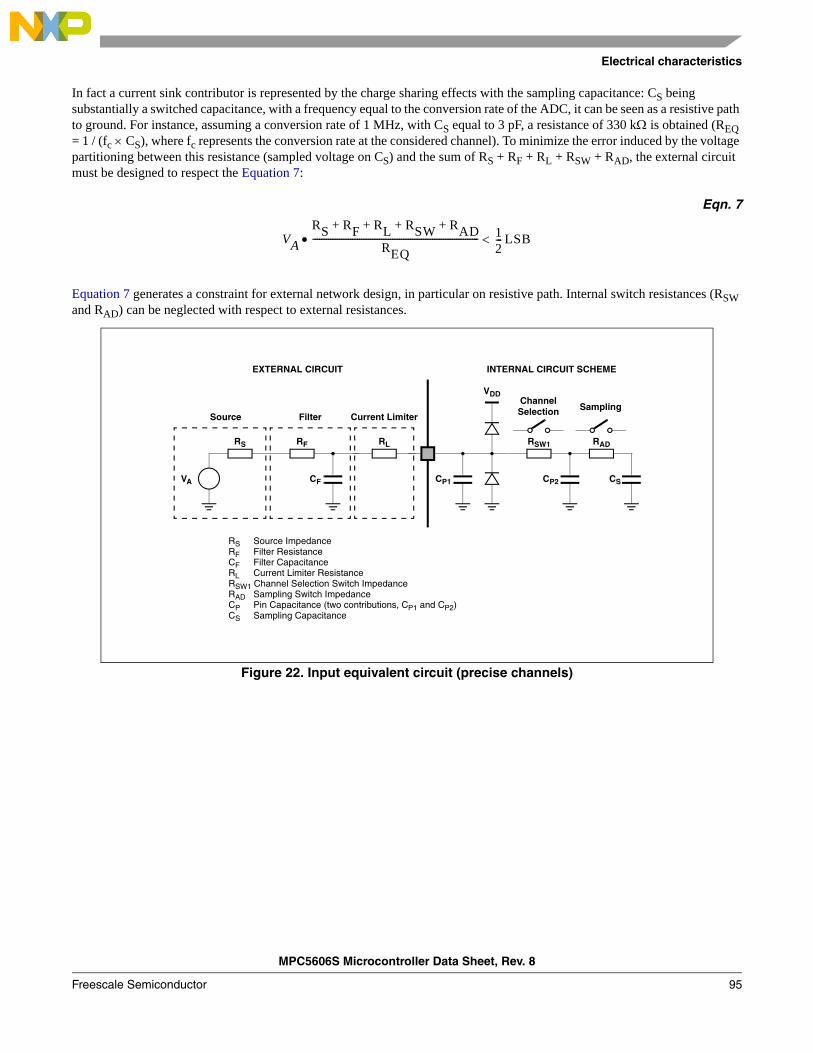
Electrical characteristics
MPC5606S Microcontroller Data Sheet, Rev. 8
Freescale Semiconductor 95
In fact a current sink contributor is represented by the charge sharing effects with the sampling capacitance: CS being substantially a switched capacitance, with a frequency equal to the conversion rate of the ADC, it can be seen as a resistive path to ground. For instance, assuming a conversion rate of 1 MHz, with CS equal to 3 pF, a resistance of 330 k is obtained (REQ = 1 / (fc CS), where fc represents the conversion rate at the considered channel). To minimize the error induced by the voltage partitioning between this resistance (sampled voltage on CS) and the sum of RS + RF + RL + RSW + RAD, the external circuit must be designed to respect the Equation 7:
Eqn. 7
Equation 7 generates a constraint for external network design, in particular on resistive path. Internal switch resistances (RSW and RAD) can be neglected with respect to external resistances.
Figure 22. Input equivalent circuit (precise channels)
VA
RS RF RL RSW RAD+ + + +
REQ--------------------------------------------------------------------------- 1
2--- LSB
RF
CF
RS RL RSW1
CP2 CS
VDD
SamplingSource Filter Current Limiter
EXTERNAL CIRCUIT INTERNAL CIRCUIT SCHEME
RS Source ImpedanceRF Filter ResistanceCF Filter CapacitanceRL Current Limiter ResistanceRSW1 Channel Selection Switch ImpedanceRAD Sampling Switch ImpedanceCP Pin Capacitance (two contributions, CP1 and CP2)CS Sampling Capacitance
CP1
RAD
ChannelSelection
VA
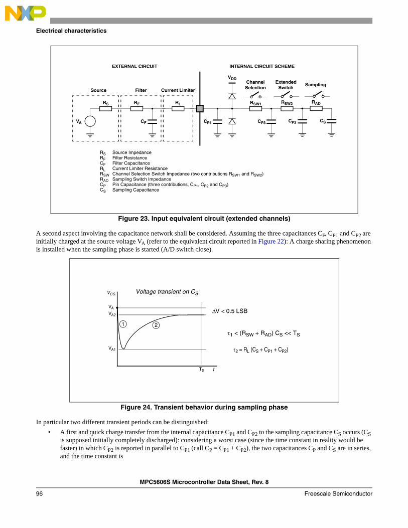
MPC5606S Microcontroller Data Sheet, Rev. 8
Electrical characteristics
Freescale Semiconductor96
Figure 23. Input equivalent circuit (extended channels)
A second aspect involving the capacitance network shall be considered. Assuming the three capacitances CF, CP1 and CP2 are initially charged at the source voltage VA (refer to the equivalent circuit reported in Figure 22): A charge sharing phenomenon is installed when the sampling phase is started (A/D switch close).
Figure 24. Transient behavior during sampling phase
In particular two different transient periods can be distinguished:
• A first and quick charge transfer from the internal capacitance CP1 and CP2 to the sampling capacitance CS occurs (CS is supposed initially completely discharged): considering a worst case (since the time constant in reality would be faster) in which CP2 is reported in parallel to CP1 (call CP = CP1 + CP2), the two capacitances CP and CS are in series, and the time constant is
RF
CF
RS RL RSW1
CP3 CS
VDD
SamplingSource Filter Current Limiter
EXTERNAL CIRCUIT INTERNAL CIRCUIT SCHEME
RS Source ImpedanceRF Filter ResistanceCF Filter CapacitanceRL Current Limiter ResistanceRSW Channel Selection Switch Impedance (two contributions RSW1 and RSW2)RAD Sampling Switch ImpedanceCP Pin Capacitance (three contributions, CP1, CP2 and CP3)CS Sampling Capacitance
CP1
RAD
ChannelSelection
VA CP2
Extended
RSW2
Switch
VA
VA1
VA2
tTS
VCS Voltage transient on CS
V <0.5 LSB
1 2
1 < (RSW + RAD) CS << TS
2 = RL (CS + CP1 + CP2)
Electrical characteristics
MPC5606S Microcontroller Data Sheet, Rev. 8
Freescale Semiconductor 97
Eqn. 8
Equation 8 can again be simplified considering only CS as an additional worst condition. In reality, the transient is faster, but the A/D converter circuitry has been designed to be robust also in the very worst case: the sampling time TS is always much longer than the internal time constant:
Eqn. 9
The charge of CP1 and CP2 is redistributed also on CS, determining a new value of the voltage VA1 on the capacitance according to Equation 10:
Eqn. 10
• A second charge transfer involves also CF (that is typically bigger than the on-chip capacitance) through the resistance RL: again considering the worst case in which CP2 and CS were in parallel to CP1 (since the time constant in reality would be faster), the time constant is:
Eqn. 11
In this case, the time constant depends on the external circuit: in particular imposing that the transient is completed well before the end of sampling time TS, a constraints on RL sizing is obtained:
Eqn. 12
Of course, RL shall be sized also according to the current limitation constraints, in combination with RS (source impedance) and RF (filter resistance). Being CF definitively bigger than CP1, CP2 and CS, then the final voltage VA2 (at the end of the charge transfer transient) will be much higher than VA1. Equation 13 must be respected (charge balance assuming now CS already charged at VA1):
Eqn. 13
The two transients above are not influenced by the voltage source that, due to the presence of the RFCF filter, is not able to provide the extra charge to compensate the voltage drop on CS with respect to the ideal source VA; the time constant RFCF of the filter is very high with respect to the sampling time (TS). The filter is typically designed to act as anti-aliasing.
1 RSW RAD+ =CP CS
CP CS+---------------------
1 RSW RAD+ CS TS«
VA1 CS CP1 CP2+ + VA CP1 CP2+ =
2 RL CS CP1 CP2+ +
10 2 10 RL CS CP1 CP2+ + = TS
VA2 CS CP1 CP2 CF+ + + VA CF VA1+ CP1 CP2+ CS+ =
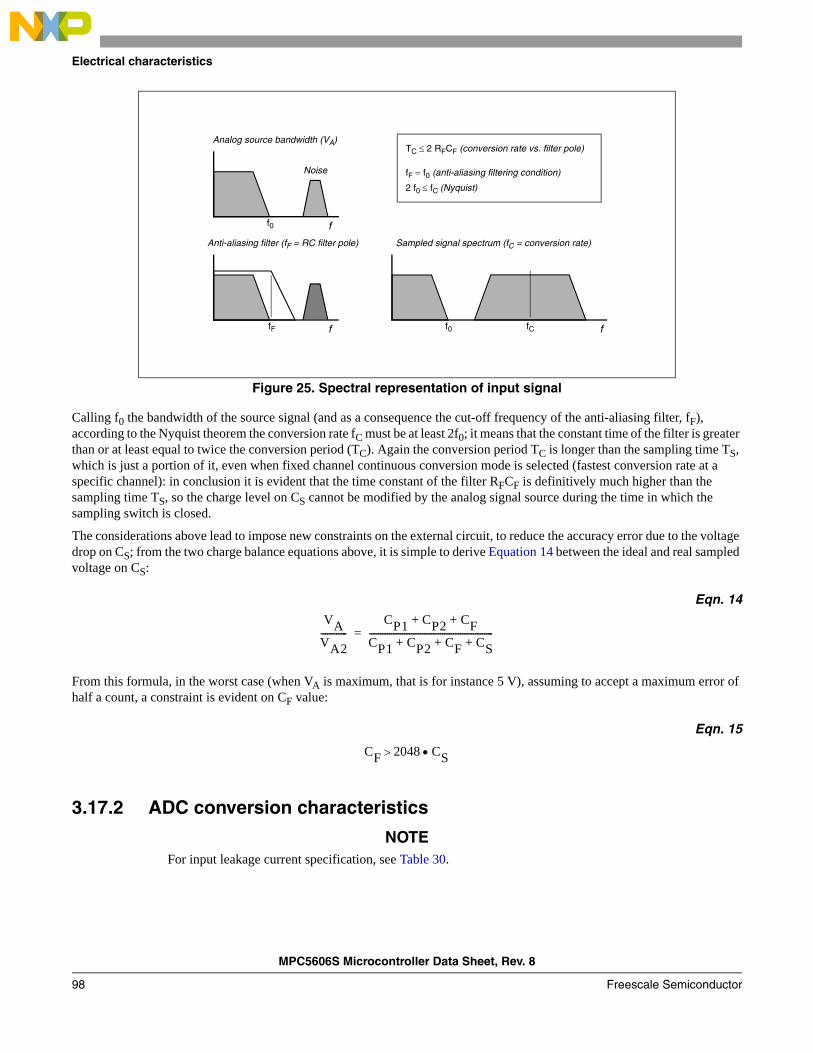
MPC5606S Microcontroller Data Sheet, Rev. 8
Electrical characteristics
Freescale Semiconductor98
Figure 25. Spectral representation of input signal
Calling f0 the bandwidth of the source signal (and as a consequence the cut-off frequency of the anti-aliasing filter, fF), according to the Nyquist theorem the conversion rate fC must be at least 2f0; it means that the constant time of the filter is greater than or at least equal to twice the conversion period (TC). Again the conversion period TC is longer than the sampling time TS, which is just a portion of it, even when fixed channel continuous conversion mode is selected (fastest conversion rate at a specific channel): in conclusion it is evident that the time constant of the filter RFCF is definitively much higher than the sampling time TS, so the charge level on CS cannot be modified by the analog signal source during the time in which the sampling switch is closed.
The considerations above lead to impose new constraints on the external circuit, to reduce the accuracy error due to the voltage drop on CS; from the two charge balance equations above, it is simple to derive Equation 14 between the ideal and real sampled voltage on CS:
Eqn. 14
From this formula, in the worst case (when VA is maximum, that is for instance 5 V), assuming to accept a maximum error of half a count, a constraint is evident on CF value:
Eqn. 15
3.17.2 ADC conversion characteristics
NOTEFor input leakage current specification, see Table 30.
f0 f
Analog source bandwidth (VA)
f0 f
Sampled signal spectrum (fC = conversion rate)
fCf
Anti-aliasing filter (fF = RC filter pole)
fF
2 f0 fC (Nyquist)
fF f0 (anti-aliasing filtering condition)
TC 2 RFCF (conversion rate vs. filter pole)
Noise
VAVA2------------
CP1 CP2+ CF+
CP1 CP2+ CF CS+ +--------------------------------------------------------=
CF 2048 CS
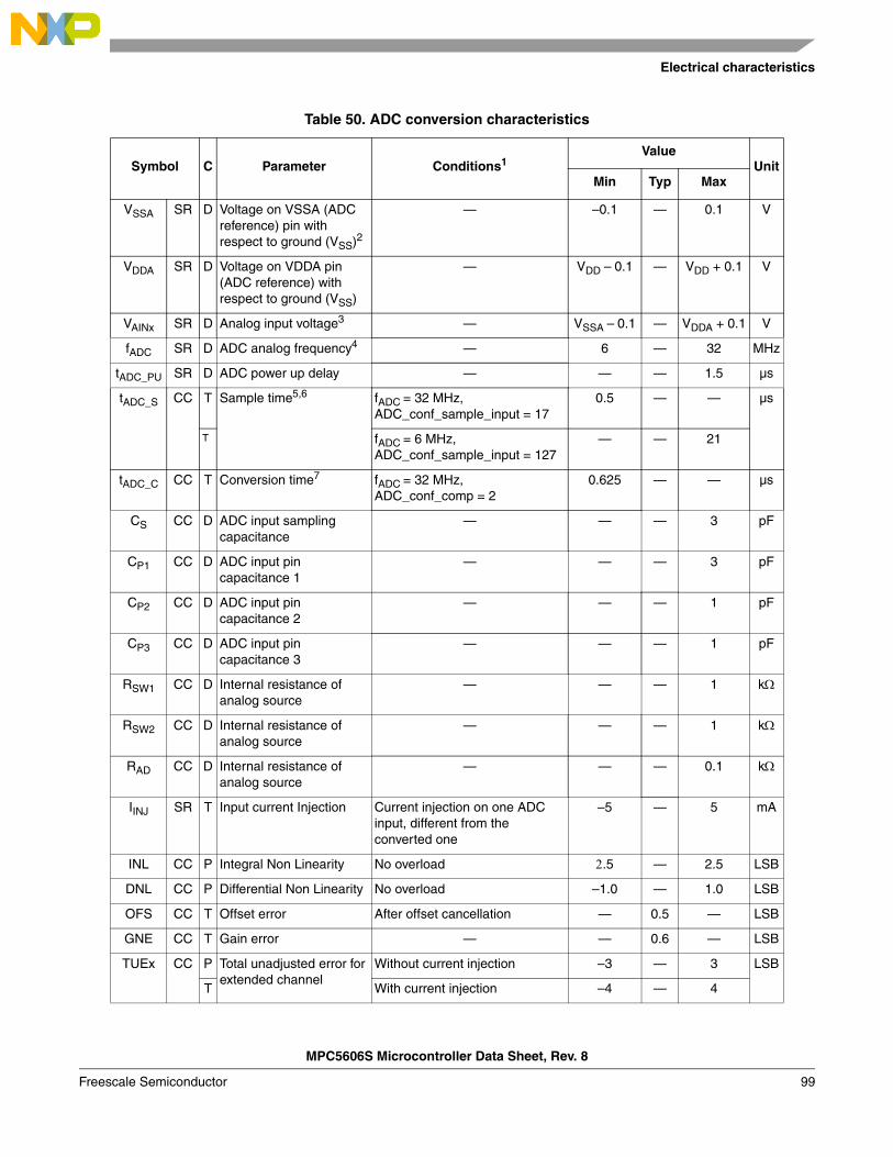
Electrical characteristics
MPC5606S Microcontroller Data Sheet, Rev. 8
Freescale Semiconductor 99
Table 50. ADC conversion characteristics
Symbol C Parameter Conditions1Value
UnitMin Typ Max
VSSA SR D Voltage on VSSA (ADC reference) pin with respect to ground (VSS)2
— –0.1 — 0.1 V
VDDA SR D Voltage on VDDA pin (ADC reference) with respect to ground (VSS)
— VDD – 0.1 — VDD + 0.1 V
VAINx SR D Analog input voltage3 — VSSA – 0.1 — VDDA + 0.1 V
fADC SR D ADC analog frequency4 — 6 — 32 MHz
tADC_PU SR D ADC power up delay — — — 1.5 µs
tADC_S CC T Sample time5,6 fADC = 32 MHz,ADC_conf_sample_input = 17
0.5 — — µs
T fADC = 6 MHz,ADC_conf_sample_input = 127
— — 21
tADC_C CC T Conversion time7 fADC = 32 MHz,ADC_conf_comp = 2
0.625 — — µs
CS CC D ADC input sampling capacitance
— — — 3 pF
CP1 CC D ADC input pin capacitance 1
— — — 3 pF
CP2 CC D ADC input pin capacitance 2
— — — 1 pF
CP3 CC D ADC input pin capacitance 3
— — — 1 pF
RSW1 CC D Internal resistance of analog source
— — — 1 k
RSW2 CC D Internal resistance of analog source
— — — 1 k
RAD CC D Internal resistance of analog source
— — — 0.1 k
IINJ SR T Input current Injection Current injection on one ADC input, different from the converted one
–5 — 5 mA
INL CC P Integral Non Linearity No overload .5 — 2.5 LSB
DNL CC P Differential Non Linearity No overload –1.0 — 1.0 LSB
OFS CC T Offset error After offset cancellation — 0.5 — LSB
GNE CC T Gain error — — 0.6 — LSB
TUEx CC P Total unadjusted error for extended channel
Without current injection –3 — 3 LSB
T With current injection –4 — 4
MPC5606S Microcontroller Data Sheet, Rev. 8
Electrical characteristics
Freescale Semiconductor100
3.18 LCD driver electrical characteristics
3.19 Pad AC specifications
1 VDDA = 3.3 V ±10% / 5.0 V ±10%, TA = –40 to 105 °C, unless otherwise specified.2 Analog and digital VSS must be common (to be tied together externally).3 VAINx may exceed VSSA and VDDA limits, remaining on absolute maximum ratings, but the results of the conversion
will be clamped respectively to 0x000 or 0x3FF. 4 At 32 MHz the minimum sampling time must be at least 180 ns. 5 During the sample time the input capacitance CS can be charged/discharged by the external source. The internal
resistance of the analog source must allow the capacitance to reach its final voltage level within tADC_S. After the end of the sample time tADC_S, changes of the analog input voltage have no effect on the conversion result. Values for the sample clock tADC_S depend on programming.
6 The maximum sample rate is 1 million samples per second, provided the source impedance and current limiter(> 1 k) are calculated adequately. — Filter capacitor at analog source output must meet the criteria Cf (filter capacitor) > 2048 × Cs (sampling capacitor is 3 pF).
7 This parameter does not include the sample time tADC_S, but only the time for determining the digital result and the time to load the result’s register with the conversion result.
Table 51. LCD driver specifications
Symbol C ParameterValue1
1 VDD = 5.0 V ± 10%, TA = –40–105 °C, unless otherwise specified
UnitMin Typ Max
VLCD SR C Voltage on VLCD (LCD supply) pin with respect to VSS
0 — VDDE + 0.3 V
ZBP/FP CC T LCD output impedance (BP[n-1:0],FP[m-1:0]) for output levels VLCD, VSS2
2 Outputs measured one at a time, low impedance voltage source connected to the VLCD pin.
— — 5.0 k
IBP/FP CC T LCD output current (BP[n-1:0],FP[m-1:0]) for outputs charge/discharge voltage levels VLCD2/3, VLCD1/2, VLCD1/3)2,3
3 With PWR=10, BSTEN=0, and BSTAO=0
— 25 — A
Table 52. Pad AC specifications (5.0 V, PAD3V5V = 0)1
No. Pad
Tswitchon1
(ns)Rise/Fall2
(ns)Frequency
(MHz)Current slew
(mA/ns) Load drive(pF)
Min Typ Max Min Typ Max Min Typ Max Min Typ Max
1 Slow 1.5 — 30 6 — 50 — — 4 0.04 — 2 25
1.5 — 30 9 — 100 — — 2 0.04 — 2 50
1.5 — 30 12 — 125 — — 2 0.04 — 2 100
1.5 — 30 16 — 150 — — 2 0.04 — 2 200
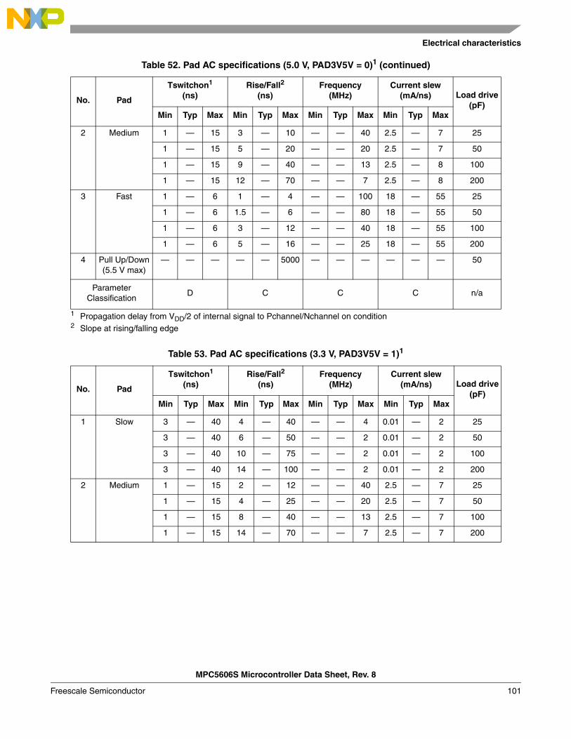
Electrical characteristics
MPC5606S Microcontroller Data Sheet, Rev. 8
Freescale Semiconductor 101
2 Medium 1 — 15 3 — 10 — — 40 2.5 — 7 25
1 — 15 5 — 20 — — 20 2.5 — 7 50
1 — 15 9 — 40 — — 13 2.5 — 8 100
1 — 15 12 — 70 — — 7 2.5 — 8 200
3 Fast 1 — 6 1 — 4 — — 100 18 — 55 25
1 — 6 1.5 — 6 — — 80 18 — 55 50
1 — 6 3 — 12 — — 40 18 — 55 100
1 — 6 5 — 16 — — 25 18 — 55 200
4 Pull Up/Down(5.5 V max)
— — — — — 5000 — — — — — — 50
Parameter Classification
D C C C n/a
1 Propagation delay from VDD/2 of internal signal to Pchannel/Nchannel on condition2 Slope at rising/falling edge
Table 53. Pad AC specifications (3.3 V, PAD3V5V = 1)1
No. Pad
Tswitchon1
(ns)Rise/Fall2
(ns)Frequency
(MHz)Current slew
(mA/ns) Load drive(pF)
Min Typ Max Min Typ Max Min Typ Max Min Typ Max
1 Slow 3 — 40 4 — 40 — — 4 0.01 — 2 25
3 — 40 6 — 50 — — 2 0.01 — 2 50
3 — 40 10 — 75 — — 2 0.01 — 2 100
3 — 40 14 — 100 — — 2 0.01 — 2 200
2 Medium 1 — 15 2 — 12 — — 40 2.5 — 7 25
1 — 15 4 — 25 — — 20 2.5 — 7 50
1 — 15 8 — 40 — — 13 2.5 — 7 100
1 — 15 14 — 70 — — 7 2.5 — 7 200
Table 52. Pad AC specifications (5.0 V, PAD3V5V = 0)1 (continued)
No. Pad
Tswitchon1
(ns)Rise/Fall2
(ns)Frequency
(MHz)Current slew
(mA/ns) Load drive(pF)
Min Typ Max Min Typ Max Min Typ Max Min Typ Max
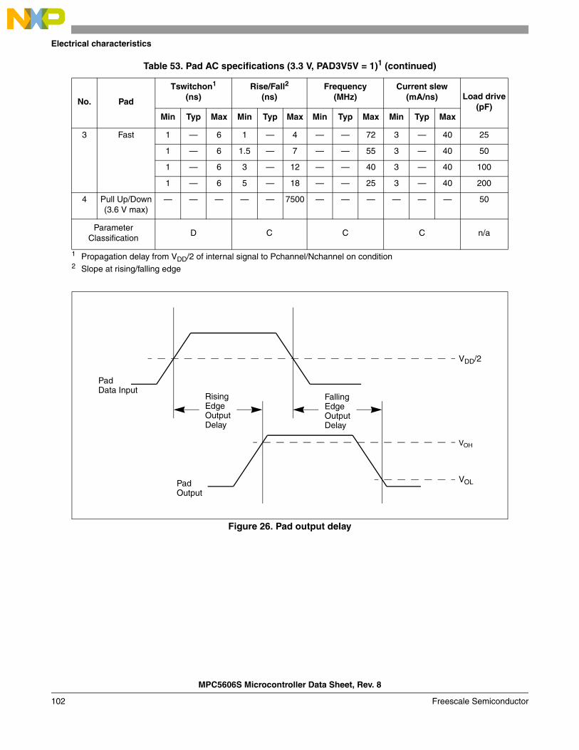
MPC5606S Microcontroller Data Sheet, Rev. 8
Electrical characteristics
Freescale Semiconductor102
Figure 26. Pad output delay
3 Fast 1 — 6 1 — 4 — — 72 3 — 40 25
1 — 6 1.5 — 7 — — 55 3 — 40 50
1 — 6 3 — 12 — — 40 3 — 40 100
1 — 6 5 — 18 — — 25 3 — 40 200
4 Pull Up/Down(3.6 V max)
— — — — — 7500 — — — — — — 50
Parameter Classification
D C C C n/a
1 Propagation delay from VDD/2 of internal signal to Pchannel/Nchannel on condition2 Slope at rising/falling edge
Table 53. Pad AC specifications (3.3 V, PAD3V5V = 1)1 (continued)
No. Pad
Tswitchon1
(ns)Rise/Fall2
(ns)Frequency
(MHz)Current slew
(mA/ns) Load drive(pF)
Min Typ Max Min Typ Max Min Typ Max Min Typ Max
VDD/2
VOH
VOL
RisingEdgeOutputDelay
FallingEdgeOutputDelay
PadData Input
PadOutput
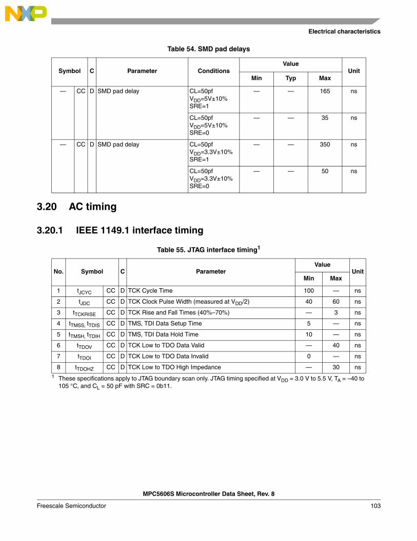
Electrical characteristics
MPC5606S Microcontroller Data Sheet, Rev. 8
Freescale Semiconductor 103
3.20 AC timing
3.20.1 IEEE 1149.1 interface timing
Table 54. SMD pad delays
Symbol C Parameter ConditionsValue
UnitMin Typ Max
— CC D SMD pad delay CL=50pfVDD=5V±10%SRE=1
— — 165 ns
CL=50pfVDD=5V±10%SRE=0
— — 35 ns
— CC D SMD pad delay CL=50pfVDD=3.3V±10%SRE=1
— — 350 ns
CL=50pfVDD=3.3V±10%SRE=0
— — 50 ns
Table 55. JTAG interface timing1
1 These specifications apply to JTAG boundary scan only. JTAG timing specified at VDD = 3.0 V to 5.5 V, TA = –40 to 105 °C, and CL = 50 pF with SRC = 0b11.
No. Symbol C ParameterValue
UnitMin Max
1 tJCYC CC D TCK Cycle Time 100 — ns
2 tJDC CC D TCK Clock Pulse Width (measured at VDD/2) 40 60 ns
3 tTCKRISE CC D TCK Rise and Fall Times (40%–70%) — 3 ns
4 tTMSS, tTDIS CC D TMS, TDI Data Setup Time 5 — ns
5 tTMSH, tTDIH CC D TMS, TDI Data Hold Time 10 — ns
6 tTDOV CC D TCK Low to TDO Data Valid — 40 ns
7 tTDOI CC D TCK Low to TDO Data Invalid 0 — ns
8 tTDOHZ CC D TCK Low to TDO High Impedance — 30 ns
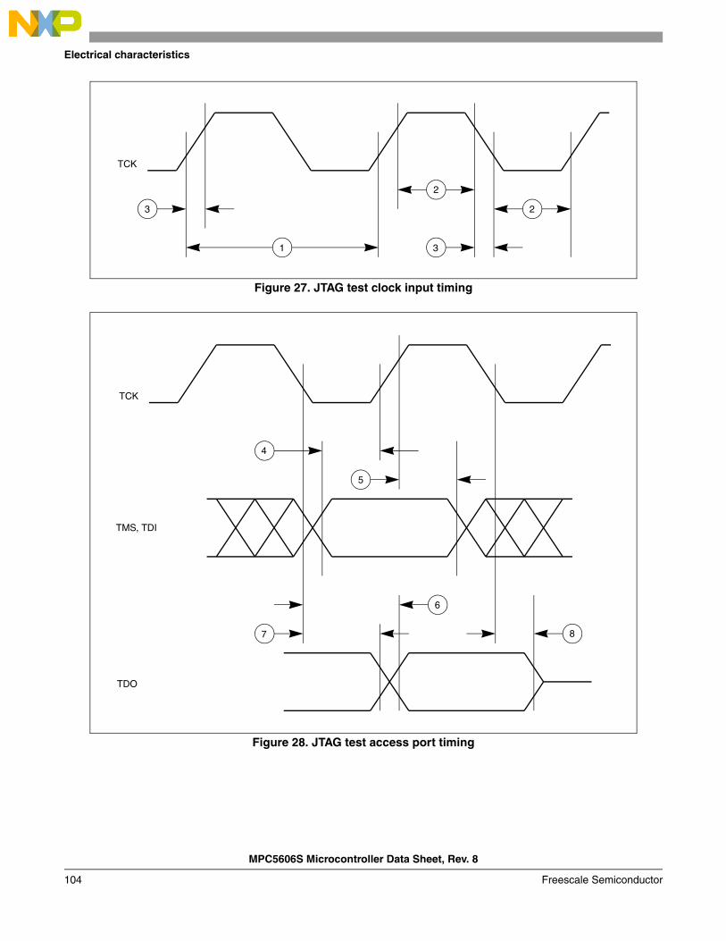
MPC5606S Microcontroller Data Sheet, Rev. 8
Electrical characteristics
Freescale Semiconductor104
Figure 27. JTAG test clock input timing
Figure 28. JTAG test access port timing
TCK
1
2
2
3
3
TCK
4
5
6
7 8
TMS, TDI
TDO
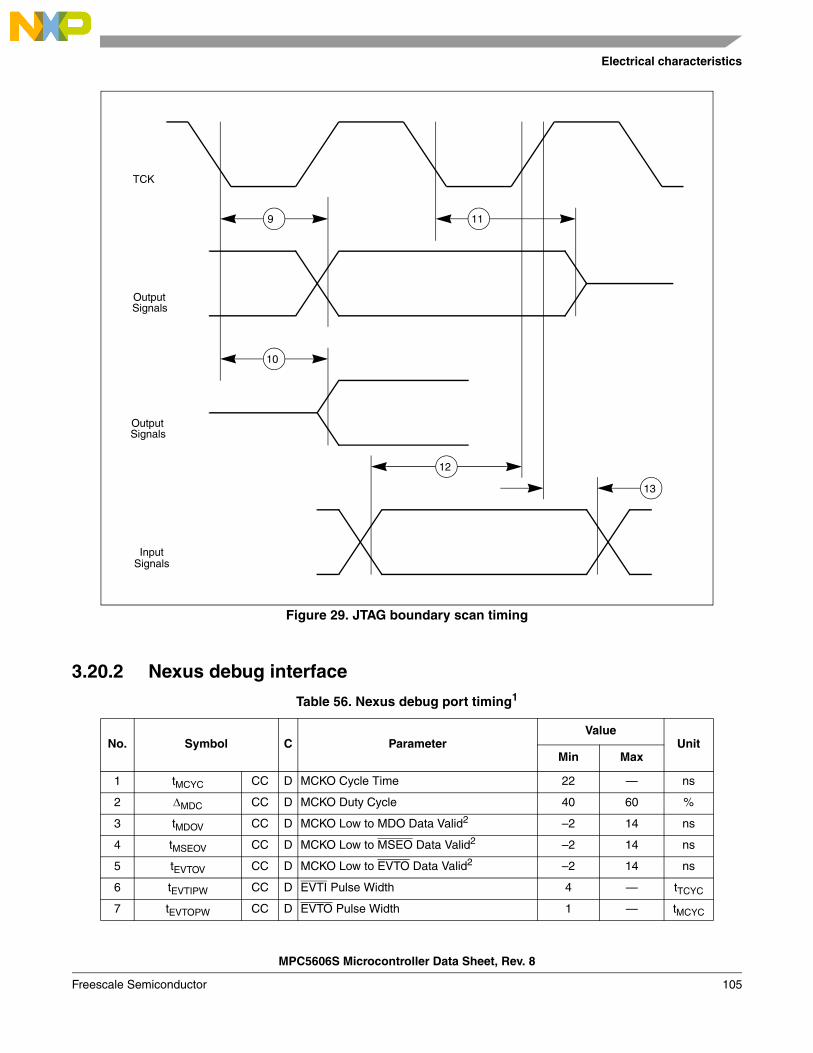
Electrical characteristics
MPC5606S Microcontroller Data Sheet, Rev. 8
Freescale Semiconductor 105
Figure 29. JTAG boundary scan timing
3.20.2 Nexus debug interface
Table 56. Nexus debug port timing1
No. Symbol C ParameterValue
UnitMin Max
1 tMCYC CC D MCKO Cycle Time 22 — ns
2 MDC CC D MCKO Duty Cycle 40 60 %
3 tMDOV CC D MCKO Low to MDO Data Valid2 –2 14 ns
4 tMSEOV CC D MCKO Low to MSEO Data Valid2 –2 14 ns
5 tEVTOV CC D MCKO Low to EVTO Data Valid2 –2 14 ns
6 tEVTIPW CC D EVTI Pulse Width 4 — tTCYC
7 tEVTOPW CC D EVTO Pulse Width 1 — tMCYC
TCK
OutputSignals
InputSignals
OutputSignals
9
10
11
12
13
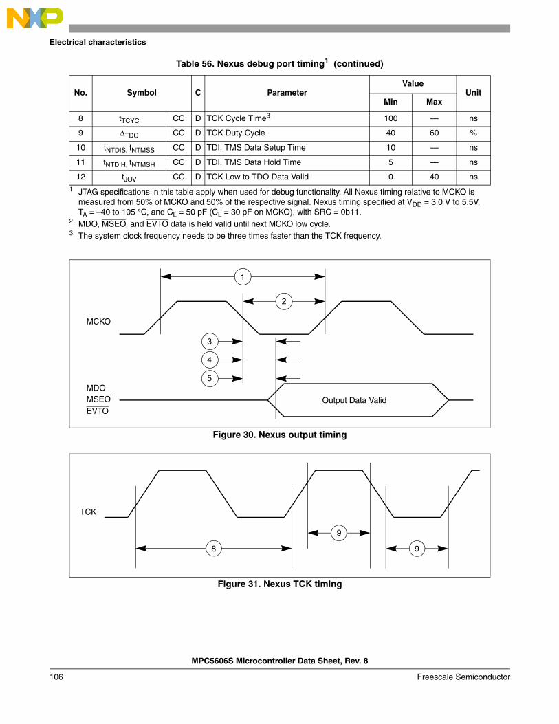
MPC5606S Microcontroller Data Sheet, Rev. 8
Electrical characteristics
Freescale Semiconductor106
Figure 30. Nexus output timing
Figure 31. Nexus TCK timing
8 tTCYC CC D TCK Cycle Time3 100 — ns
9 TDC CC D TCK Duty Cycle 40 60 %
10 tNTDIS, tNTMSS CC D TDI, TMS Data Setup Time 10 — ns
11 tNTDIH, tNTMSH CC D TDI, TMS Data Hold Time 5 — ns
12 tJOV CC D TCK Low to TDO Data Valid 0 40 ns1 JTAG specifications in this table apply when used for debug functionality. All Nexus timing relative to MCKO is
measured from 50% of MCKO and 50% of the respective signal. Nexus timing specified at VDD = 3.0 V to 5.5V, TA = –40 to 105 °C, and CL = 50 pF (CL = 30 pF on MCKO), with SRC = 0b11.
2 MDO, MSEO, and EVTO data is held valid until next MCKO low cycle.3 The system clock frequency needs to be three times faster than the TCK frequency.
Table 56. Nexus debug port timing1 (continued)
No. Symbol C ParameterValue
UnitMin Max
1
2
4
5
MCKO
MDOMSEOEVTO
Output Data Valid
3
TCK
8
9
9
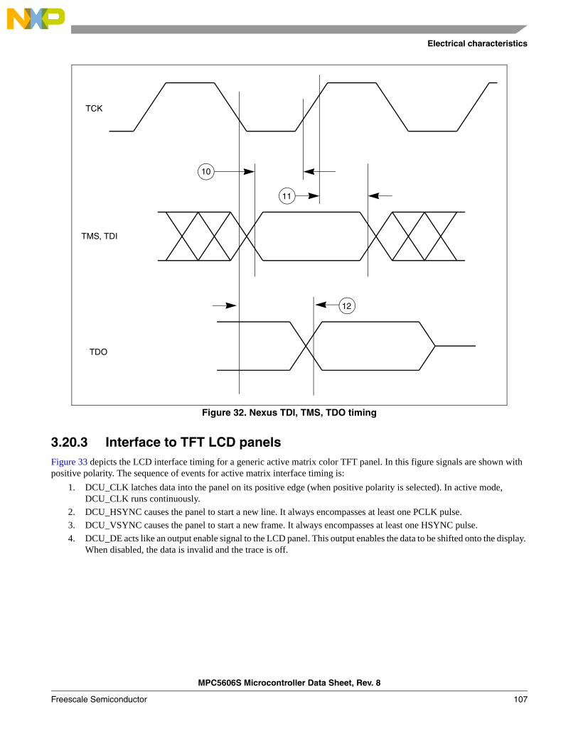
Electrical characteristics
MPC5606S Microcontroller Data Sheet, Rev. 8
Freescale Semiconductor 107
Figure 32. Nexus TDI, TMS, TDO timing
3.20.3 Interface to TFT LCD panelsFigure 33 depicts the LCD interface timing for a generic active matrix color TFT panel. In this figure signals are shown with positive polarity. The sequence of events for active matrix interface timing is:
1. DCU_CLK latches data into the panel on its positive edge (when positive polarity is selected). In active mode, DCU_CLK runs continuously.
2. DCU_HSYNC causes the panel to start a new line. It always encompasses at least one PCLK pulse.
3. DCU_VSYNC causes the panel to start a new frame. It always encompasses at least one HSYNC pulse.
4. DCU_DE acts like an output enable signal to the LCD panel. This output enables the data to be shifted onto the display. When disabled, the data is invalid and the trace is off.
TDO
10
11
TMS, TDI
12
TCK
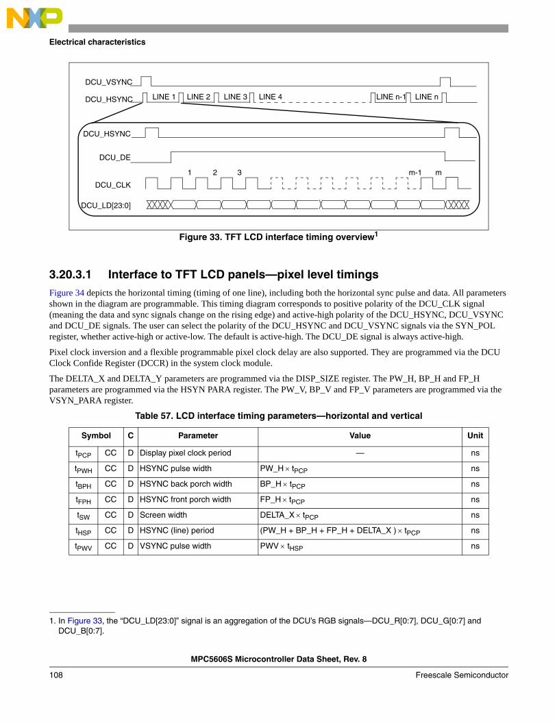
MPC5606S Microcontroller Data Sheet, Rev. 8
Electrical characteristics
Freescale Semiconductor108
Figure 33. TFT LCD interface timing overview1
3.20.3.1 Interface to TFT LCD panels—pixel level timingsFigure 34 depicts the horizontal timing (timing of one line), including both the horizontal sync pulse and data. All parameters shown in the diagram are programmable. This timing diagram corresponds to positive polarity of the DCU_CLK signal (meaning the data and sync signals change on the rising edge) and active-high polarity of the DCU_HSYNC, DCU_VSYNC and DCU_DE signals. The user can select the polarity of the DCU_HSYNC and DCU_VSYNC signals via the SYN_POL register, whether active-high or active-low. The default is active-high. The DCU_DE signal is always active-high.
Pixel clock inversion and a flexible programmable pixel clock delay are also supported. They are programmed via the DCU Clock Confide Register (DCCR) in the system clock module.
The DELTA_X and DELTA_Y parameters are programmed via the DISP_SIZE register. The PW_H, BP_H and FP_H parameters are programmed via the HSYN PARA register. The PW_V, BP_V and FP_V parameters are programmed via the VSYN_PARA register.
1. In Figure 33, the “DCU_LD[23:0]” signal is an aggregation of the DCU’s RGB signals—DCU_R[0:7], DCU_G[0:7] and DCU_B[0:7].
Table 57. LCD interface timing parameters—horizontal and vertical
Symbol C Parameter Value Unit
tPCP CC D Display pixel clock period — ns
tPWH CC D HSYNC pulse width PW_H tPCP ns
tBPH CC D HSYNC back porch width BP_H tPCP ns
tFPH CC D HSYNC front porch width FP_H tPCP ns
tSW CC D Screen width DELTA_X tPCP ns
tHSP CC D HSYNC (line) period (PW_H + BP_H + FP_H + DELTA_X ) tPCP ns
tPWV CC D VSYNC pulse width PWVtHSP ns
LINE 1 LINE 2 LINE 3 LINE 4 LINE n-1 LINE n
DCU_VSYNC
DCU_HSYNC
DCU_HSYNC
DCU_DE
DCU_CLK
DCU_LD[23:0]
21 3 m-1 m
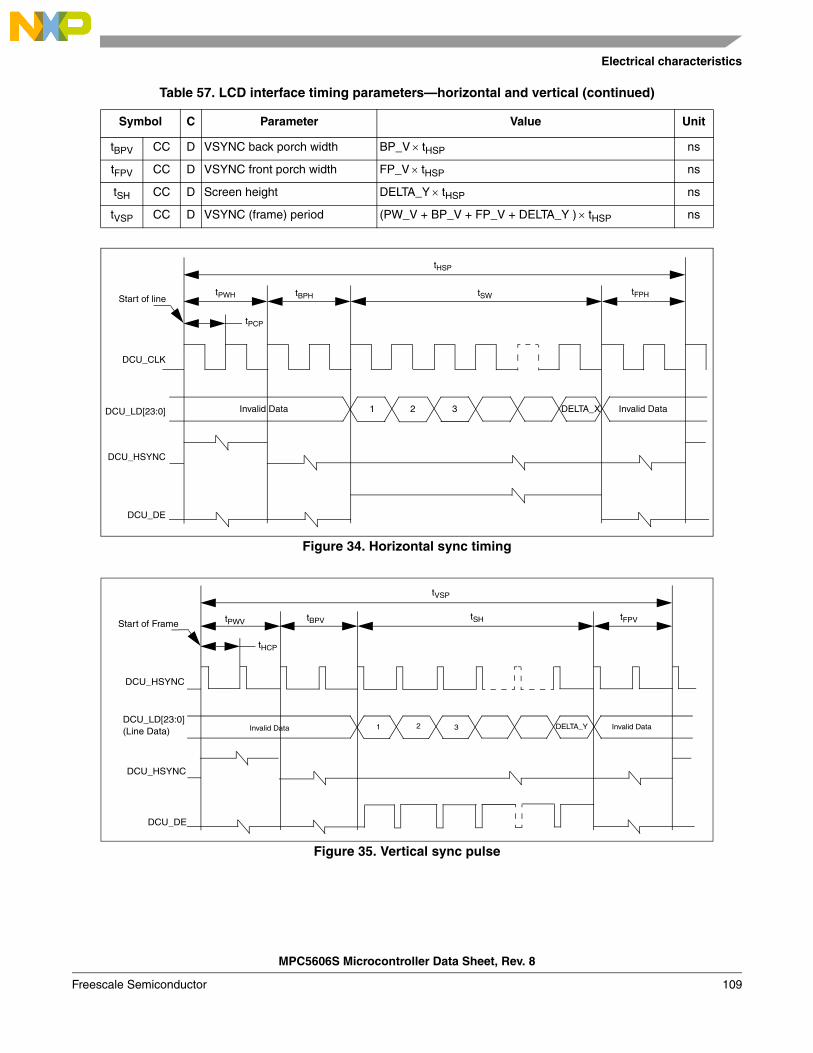
Electrical characteristics
MPC5606S Microcontroller Data Sheet, Rev. 8
Freescale Semiconductor 109
Figure 34. Horizontal sync timing
Figure 35. Vertical sync pulse
tBPV CC D VSYNC back porch width BP_V tHSP ns
tFPV CC D VSYNC front porch width FP_V tHSP ns
tSH CC D Screen height DELTA_Y tHSP ns
tVSP CC D VSYNC (frame) period (PW_V + BP_V + FP_V + DELTA_Y ) tHSP ns
Table 57. LCD interface timing parameters—horizontal and vertical (continued)
Symbol C Parameter Value Unit
Start of line
DCU_CLK
DCU_LD[23:0]
DCU_HSYNC
DCU_DE
tPWH tBPH
tHSP
tSW
tPCP
tFPH
1 2 3 DELTA_XInvalid Data Invalid Data
Start of Frame
DCU_HSYNC
DCU_LD[23:0]
DCU_HSYNC
DCU_DE
tPWV tBPV
tVSP
tHCP
tFPV
1 2 3 DELTA_YInvalid Data Invalid Data(Line Data)
tSH
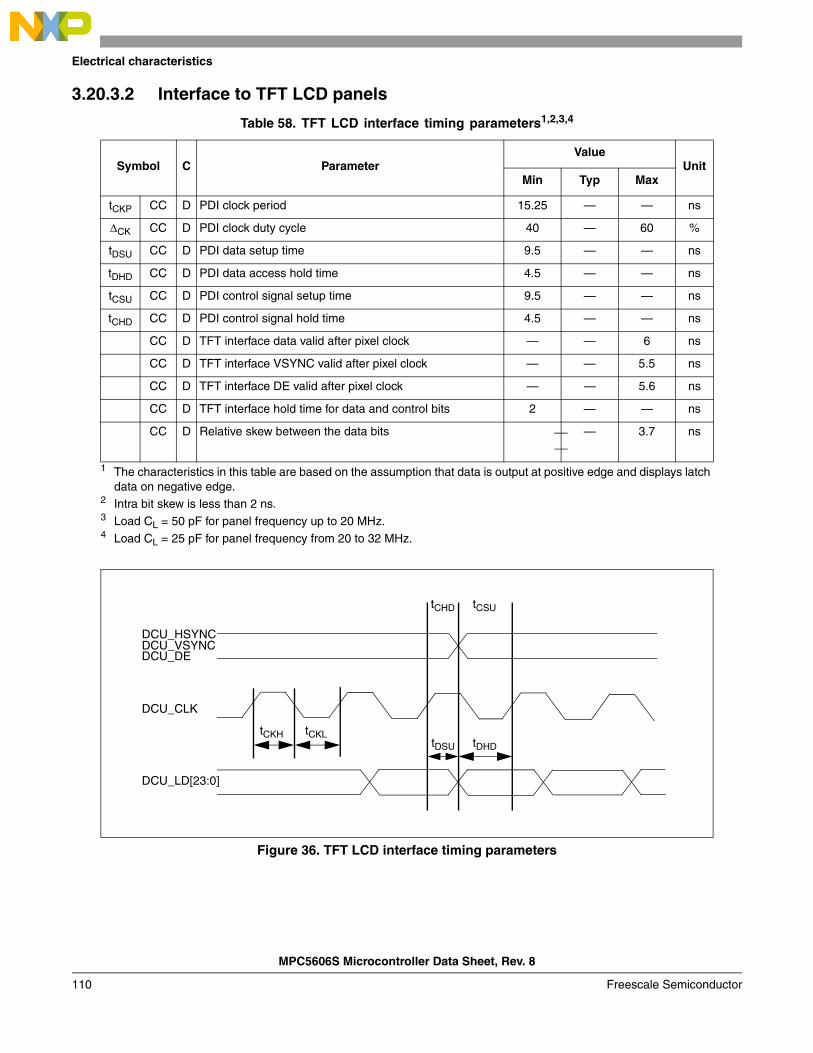
MPC5606S Microcontroller Data Sheet, Rev. 8
Electrical characteristics
Freescale Semiconductor110
3.20.3.2 Interface to TFT LCD panels
Figure 36. TFT LCD interface timing parameters
Table 58. TFT LCD interface timing parameters1,2,3,4
1 The characteristics in this table are based on the assumption that data is output at positive edge and displays latch data on negative edge.
2 Intra bit skew is less than 2 ns. 3 Load CL = 50 pF for panel frequency up to 20 MHz. 4 Load CL = 25 pF for panel frequency from 20 to 32 MHz.
Symbol C ParameterValue
UnitMin Typ Max
tCKP CC D PDI clock period 15.25 — — ns
CK CC D PDI clock duty cycle 40 — 60 %
tDSU CC D PDI data setup time 9.5 — — ns
tDHD CC D PDI data access hold time 4.5 — — ns
tCSU CC D PDI control signal setup time 9.5 — — ns
tCHD CC D PDI control signal hold time 4.5 — — ns
CC D TFT interface data valid after pixel clock — — 6 ns
CC D TFT interface VSYNC valid after pixel clock — — 5.5 ns
CC D TFT interface DE valid after pixel clock — — 5.6 ns
CC D TFT interface hold time for data and control bits 2 — — ns
CC D Relative skew between the data bits ——
— 3.7 ns
DCU_HSYNCDCU_VSYNCDCU_DE
DCU_CLK
DCU_LD[23:0]
tCKH tCKL
tCHD tCSU
tDHDtDSU
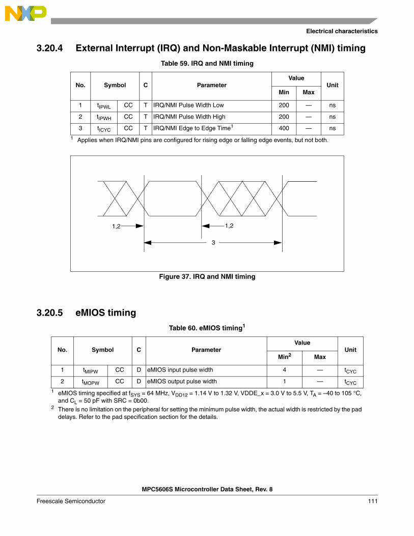
Electrical characteristics
MPC5606S Microcontroller Data Sheet, Rev. 8
Freescale Semiconductor 111
3.20.4 External Interrupt (IRQ) and Non-Maskable Interrupt (NMI) timing
Figure 37. IRQ and NMI timing
3.20.5 eMIOS timing
Table 59. IRQ and NMI timing
No. Symbol C ParameterValue
UnitMin Max
1 tIPWL CC T IRQ/NMI Pulse Width Low 200 — ns
2 tIPWH CC T IRQ/NMI Pulse Width High 200 — ns
3 tICYC CC T IRQ/NMI Edge to Edge Time1
1 Applies when IRQ/NMI pins are configured for rising edge or falling edge events, but not both.
400 — ns
Table 60. eMIOS timing1
1 eMIOS timing specified at fSYS = 64 MHz, VDD12 = 1.14 V to 1.32 V, VDDE_x = 3.0 V to 5.5 V, TA = –40 to 105 °C, and CL = 50 pF with SRC = 0b00.
No. Symbol C ParameterValue
UnitMin2
2 There is no limitation on the peripheral for setting the minimum pulse width, the actual width is restricted by the pad delays. Refer to the pad specification section for the details.
Max
1 tMIPW CC D eMIOS input pulse width 4 — tCYC
2 tMOPW CC D eMIOS output pulse width 1 — tCYC
1,2
3
1,2
MPC5606S Microcontroller Data Sheet, Rev. 8
Electrical characteristics
Freescale Semiconductor112
3.20.6 FlexCAN timingThe CAN functions are available as TX pins at normal I/O pads and as RX pins at the always on domain. There is no filter for the wakeup dominant pulse. Any high-to-low edge can cause wakeup if configured.
3.20.7 Deserial Serial Peripheral Interface (DSPI)
Table 61. FlexCAN timing1
1 FlexCAN timing specified at fSYS = 64 MHz, VDD12 = 1.14 V to 1.32 V, VDDE_x = 3.0 V to 5.5 V, TA = –40 to 105 °C, and CL = 50 pF with SRC = 0b00.
No. Symbol C ParameterValue
UnitMin Max
1 tCANOV CC D CTNX Output Valid after CLKOUT Rising Edge (Output Delay) — 22.48 ns
2 tCANSU CC D CNRX Input Valid to CLKOUT Rising Edge (Setup Time) — 12.46 ns
Table 62. DSPI timing1
No. Symbol C Parameter ConditionsValue
UnitMin Max
1 tSCK CC D DSPI Cycle TIme2,3 Master (MTFE = 0)Slave (MTFE = 0)Slave Receive Only Mode
626262
———
nsnsns
2 tCSC CC D PCS to SCK Delay4 — 20 — ns
3 tASC CC D After SCK Delay5 — 20 — ns
4 tSDC CC D SCK Duty Cycle — 0.4 x tSCK 0.6 x tSCK ns
5 tA CC D Slave Access Time(PCSx active to SOUT driven)
SS active to SOUT valid — 40 ns
6 tDIS CC D Slave SOUT Disable Time(PCSx inactive to SOUT High-Z or invalid)
SS inactive to SOUT High-Z or invalid
— 10 ns
7 tPCSC PCSx to PCSS time — 20 — ns
8 tPASC PCSS to PCSx time — 20 — ns
9 tSUI CC D Data Setup Time for Inputs Master (MTFE = 0)SlaveMaster (MTFE = 1, CPHA = 0)6
Master (MTFE = 1, CPHA = 1)
352
2035
————
nsnsnsns
10 tHI CC D Data Hold Time for Inputs Master (MTFE = 0)SlaveMaster (MTFE = 1, CPHA = 0)6
Master (MTFE = 1, CPHA = 1)
–55
10–5
————
nsnsnsns
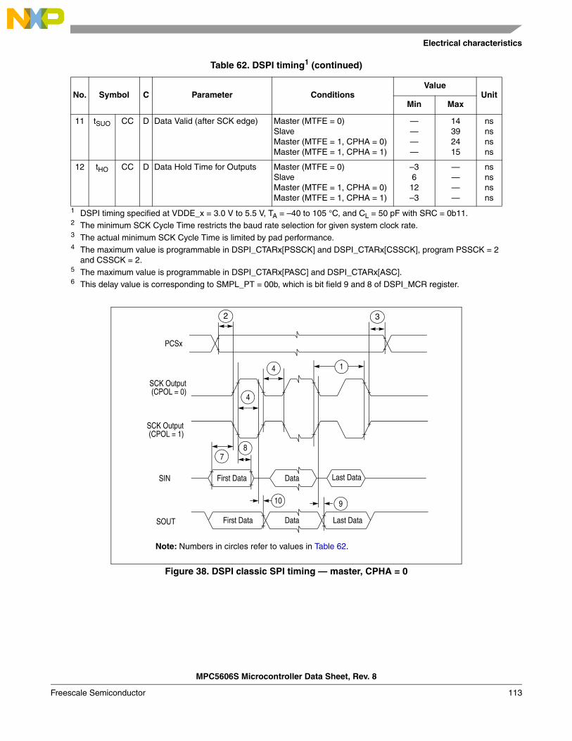
Electrical characteristics
MPC5606S Microcontroller Data Sheet, Rev. 8
Freescale Semiconductor 113
Figure 38. DSPI classic SPI timing — master, CPHA = 0
11 tSUO CC D Data Valid (after SCK edge) Master (MTFE = 0)Slave Master (MTFE = 1, CPHA = 0)Master (MTFE = 1, CPHA = 1)
————
14392415
nsnsnsns
12 tHO CC D Data Hold Time for Outputs Master (MTFE = 0)SlaveMaster (MTFE = 1, CPHA = 0)Master (MTFE = 1, CPHA = 1)
–36
12–3
————
nsnsnsns
1 DSPI timing specified at VDDE_x = 3.0 V to 5.5 V, TA = –40 to 105 °C, and CL = 50 pF with SRC = 0b11. 2 The minimum SCK Cycle Time restricts the baud rate selection for given system clock rate.3 The actual minimum SCK Cycle Time is limited by pad performance.4 The maximum value is programmable in DSPI_CTARx[PSSCK] and DSPI_CTARx[CSSCK], program PSSCK = 2
and CSSCK = 2. 5 The maximum value is programmable in DSPI_CTARx[PASC] and DSPI_CTARx[ASC]. 6 This delay value is corresponding to SMPL_PT = 00b, which is bit field 9 and 8 of DSPI_MCR register.
Table 62. DSPI timing1 (continued)
No. Symbol C Parameter ConditionsValue
UnitMin Max
Data Last DataFirst Data
First Data Data Last Data
SIN
SOUT
PCSx
SCK Output
4
7
10
1
9
8
4
SCK Output
(CPOL = 0)
(CPOL = 1)
32
Note: Numbers in circles refer to values in Table 62.
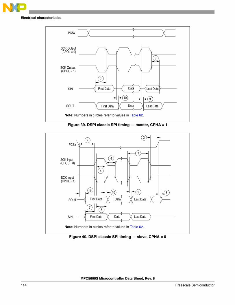
MPC5606S Microcontroller Data Sheet, Rev. 8
Electrical characteristics
Freescale Semiconductor114
Figure 39. DSPI classic SPI timing — master, CPHA = 1
Figure 40. DSPI classic SPI timing — slave, CPHA = 0
Data Last DataFirst DataSIN
SOUT
10 9
8
Last DataDataFirst Data
SCK Output
SCK Output
PCSx
7
(CPOL = 0)
(CPOL = 1)
Note: Numbers in circles refer to values in Table 62.
Last DataFirst Data
3
4
1
Data
Data
SIN
SOUT
PCSx
4
5 6
7
9
8
10
SCK Input
First Data Last Data
SCK Input
2
(CPOL = 0)
(CPOL = 1)
Note: Numbers in circles refer to values in Table 62.
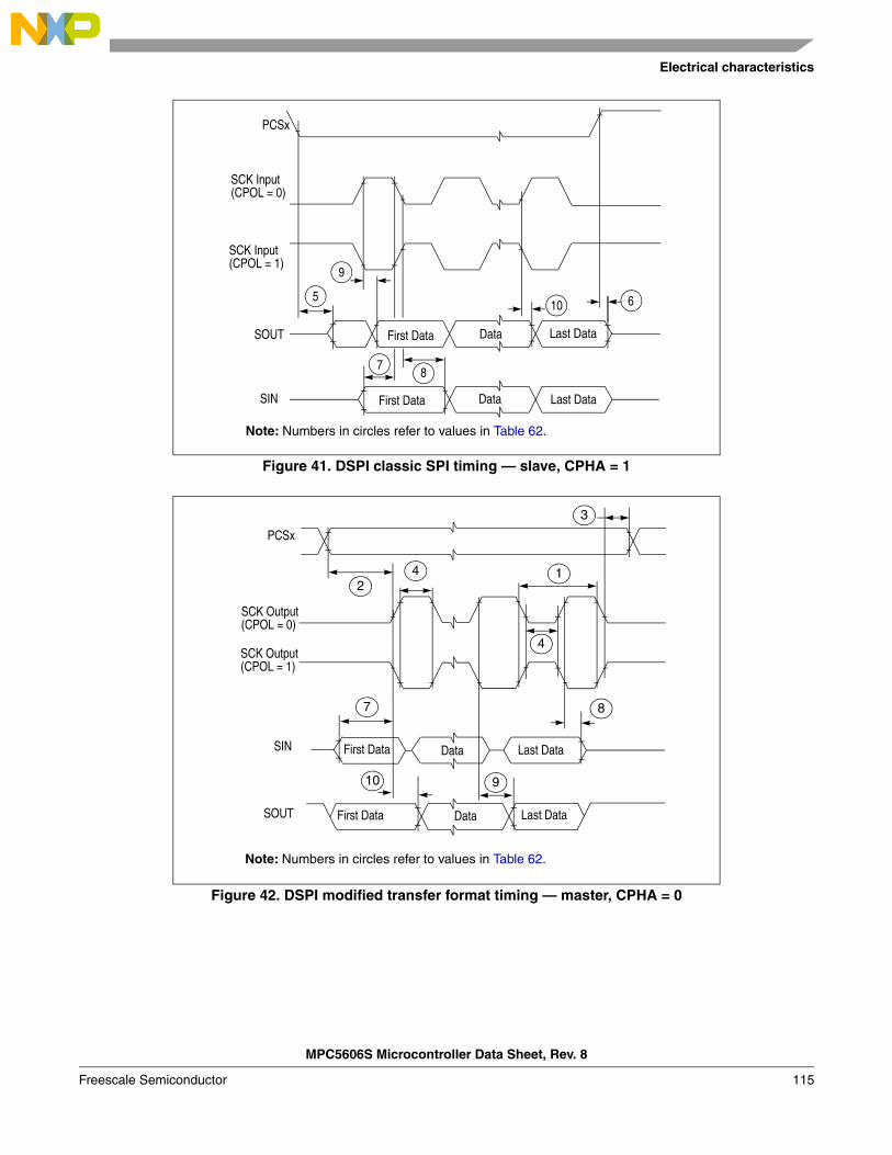
Electrical characteristics
MPC5606S Microcontroller Data Sheet, Rev. 8
Freescale Semiconductor 115
Figure 41. DSPI classic SPI timing — slave, CPHA = 1
Figure 42. DSPI modified transfer format timing — master, CPHA = 0
5 6
7
10
9
8
Last Data
Last DataSIN
SOUT
PCSx
First Data
First Data
Data
Data
SCK Input
SCK Input
(CPOL = 0)
(CPOL = 1)
Note: Numbers in circles refer to values in Table 62.
PCSx
3
14
8
4
7
10 9
SCK Output
SCK Output
SIN
SOUT
First Data Data Last Data
First Data Data Last Data
2
(CPOL = 0)
(CPOL = 1)
Note: Numbers in circles refer to values in Table 62.
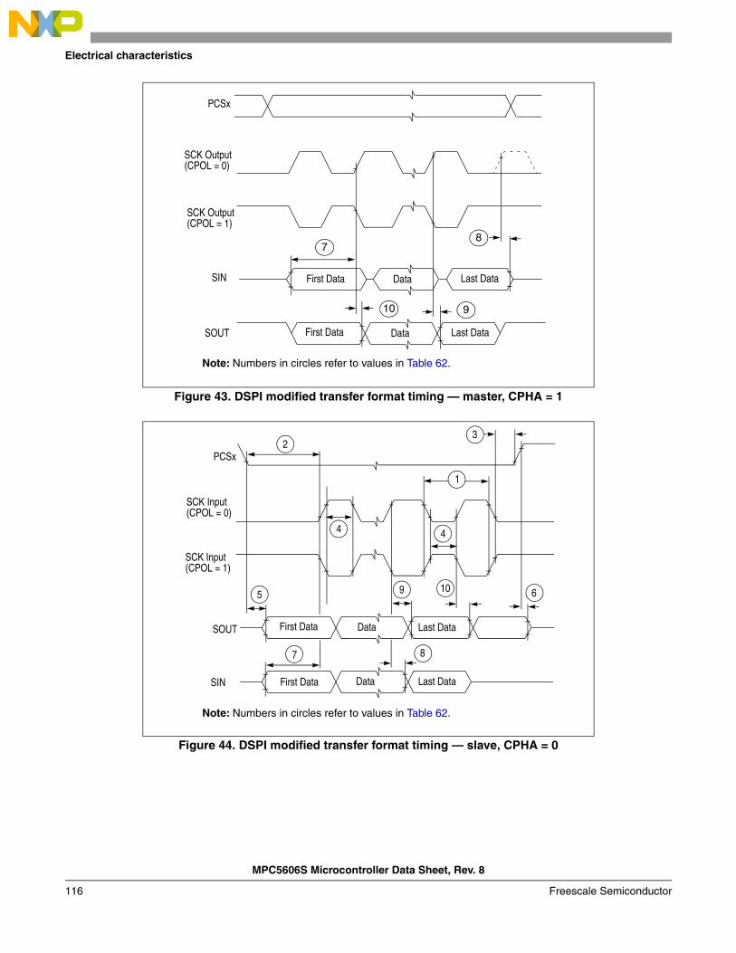
MPC5606S Microcontroller Data Sheet, Rev. 8
Electrical characteristics
Freescale Semiconductor116
Figure 43. DSPI modified transfer format timing — master, CPHA = 1
Figure 44. DSPI modified transfer format timing — slave, CPHA = 0
PCSx
87
10 9
SCK Output
SCK Output
SIN
SOUT
First Data Data Last Data
First Data Data Last Data
(CPOL = 0)
(CPOL = 1)
Note: Numbers in circles refer to values in Table 62.
Last DataFirst Data
3
4
1
Data
Data
SIN
SOUT
PCSx
4
5 6
7
9
8
SCK Input
First Data Last Data
SCK Input
2
(CPOL = 0)
(CPOL = 1)
10
Note: Numbers in circles refer to values in Table 62.
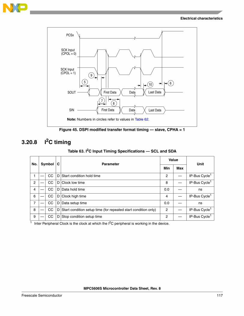
Electrical characteristics
MPC5606S Microcontroller Data Sheet, Rev. 8
Freescale Semiconductor 117
Figure 45. DSPI modified transfer format timing — slave, CPHA = 1
3.20.8 I2C timing
Table 63. I2C Input Timing Specifications — SCL and SDA
No. Symbol C ParameterValue
UnitMin Max
1 — CC D Start condition hold time 2 — IP-Bus Cycle1
1 Inter Peripheral Clock is the clock at which the I2C peripheral is working in the device.
2 — CC D Clock low time 8 — IP-Bus Cycle1
4 — CC D Data hold time 0.0 — ns
6 — CC D Clock high time 4 — IP-Bus Cycle1
7 — CC D Data setup time 0.0 — ns
8 — CC D Start condition setup time (for repeated start condition only) 2 — IP-Bus Cycle1
9 — CC D Stop condition setup time 2 — IP-Bus Cycle1
5 6
7
10
9
8
Last Data
Last DataSIN
SOUT
PCSx
First Data
First Data
Data
Data
SCK Input
SCK Input
(CPOL = 0)
(CPOL = 1)
Note: Numbers in circles refer to values in Table 62.
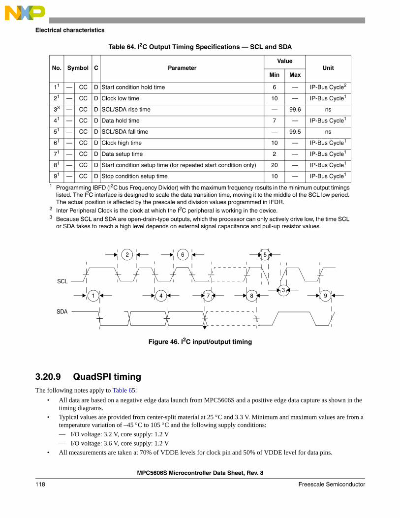
MPC5606S Microcontroller Data Sheet, Rev. 8
Electrical characteristics
Freescale Semiconductor118
Figure 46. I2C input/output timing
3.20.9 QuadSPI timingThe following notes apply to Table 65:
• All data are based on a negative edge data launch from MPC5606S and a positive edge data capture as shown in the timing diagrams.
• Typical values are provided from center-split material at 25 C and 3.3 V. Minimum and maximum values are from a temperature variation of –45 C to 105 C and the following supply conditions:
— I/O voltage: 3.2 V, core supply: 1.2 V
— I/O voltage: 3.6 V, core supply: 1.2 V
• All measurements are taken at 70% of VDDE levels for clock pin and 50% of VDDE level for data pins.
Table 64. I2C Output Timing Specifications — SCL and SDA
No. Symbol C ParameterValue
UnitMin Max
11
1 Programming IBFD (I2C bus Frequency Divider) with the maximum frequency results in the minimum output timings listed. The I2C interface is designed to scale the data transition time, moving it to the middle of the SCL low period. The actual position is affected by the prescale and division values programmed in IFDR.
— CC D Start condition hold time 6 — IP-Bus Cycle2
2 Inter Peripheral Clock is the clock at which the I2C peripheral is working in the device.
21 — CC D Clock low time 10 — IP-Bus Cycle1
33
3 Because SCL and SDA are open-drain-type outputs, which the processor can only actively drive low, the time SCL or SDA takes to reach a high level depends on external signal capacitance and pull-up resistor values.
— CC D SCL/SDA rise time — 99.6 ns
41 — CC D Data hold time 7 — IP-Bus Cycle1
51 — CC D SCL/SDA fall time — 99.5 ns
61 — CC D Clock high time 10 — IP-Bus Cycle1
71 — CC D Data setup time 2 — IP-Bus Cycle1
81 — CC D Start condition setup time (for repeated start condition only) 20 — IP-Bus Cycle1
91 — CC D Stop condition setup time 10 — IP-Bus Cycle1
SCL
SDA
1
2
34
56
7 8 9
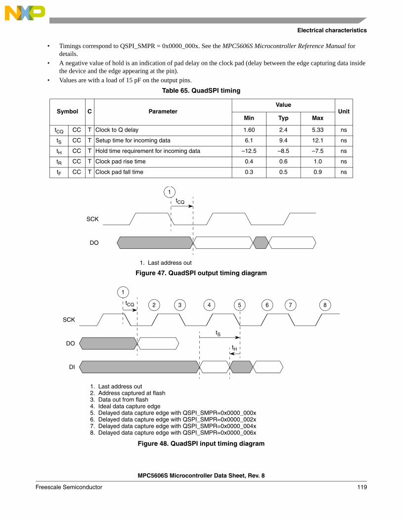
Electrical characteristics
MPC5606S Microcontroller Data Sheet, Rev. 8
Freescale Semiconductor 119
• Timings correspond to QSPI_SMPR = 0x0000_000x. See the MPC5606S Microcontroller Reference Manual for details.
• A negative value of hold is an indication of pad delay on the clock pad (delay between the edge capturing data inside the device and the edge appearing at the pin).
• Values are with a load of 15 pF on the output pins.
Figure 47. QuadSPI output timing diagram
Figure 48. QuadSPI input timing diagram
Table 65. QuadSPI timing
Symbol C ParameterValue
UnitMin Typ Max
tCQ CC T Clock to Q delay 1.60 2.4 5.33 ns
tS CC T Setup time for incoming data 6.1 9.4 12.1 ns
tH CC T Hold time requirement for incoming data –12.5 –8.5 –7.5 ns
tR CC T Clock pad rise time 0.4 0.6 1.0 ns
tF CC T Clock pad fall time 0.3 0.5 0.9 ns
SCK
tCQ
DO
1. Last address out
1
tCQ
SCK
tH
tS
DO
DI
1. Last address out2. Address captured at flash3. Data out from flash4. Ideal data capture edge5. Delayed data capture edge with QSPI_SMPR=0x0000_000x6. Delayed data capture edge with QSPI_SMPR=0x0000_002x7. Delayed data capture edge with QSPI_SMPR=0x0000_004x8. Delayed data capture edge with QSPI_SMPR=0x0000_006x
2 3 4 5 6 7 8
1
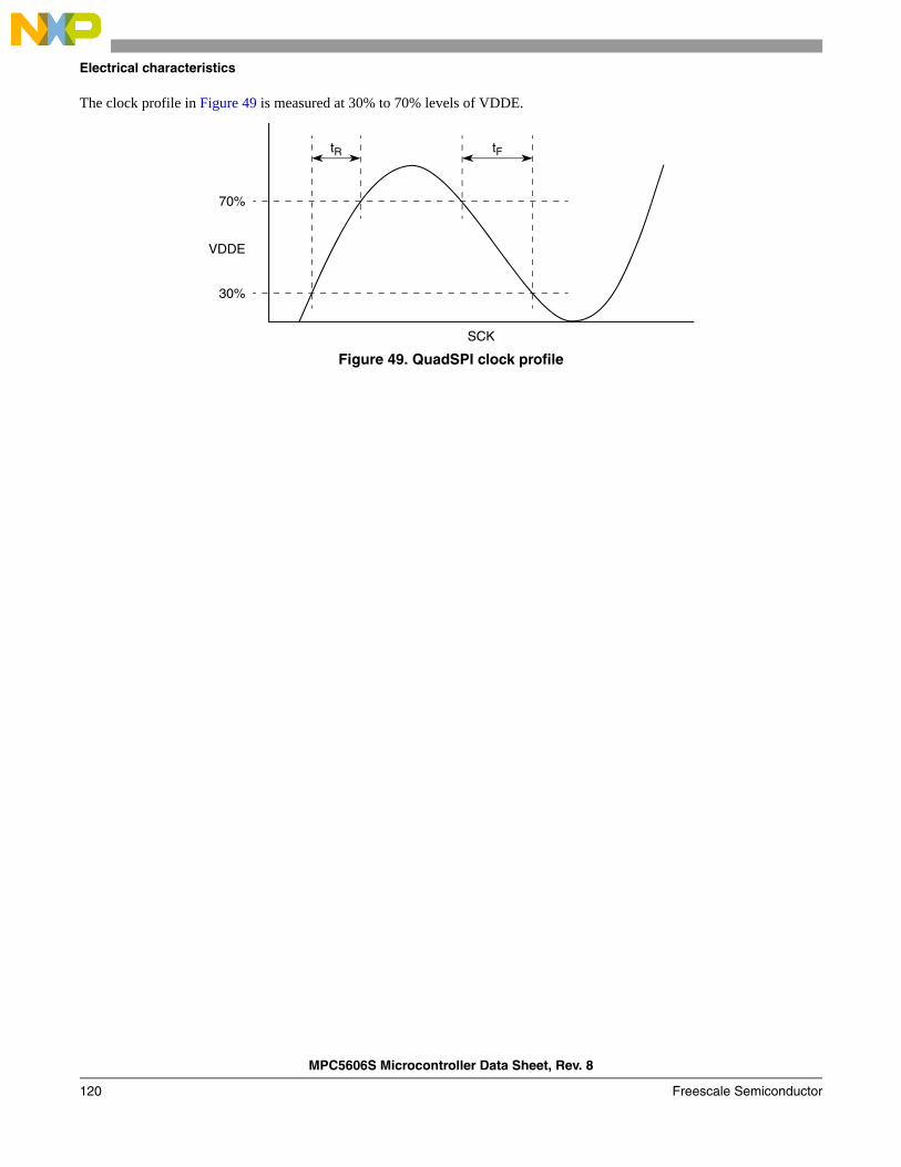
MPC5606S Microcontroller Data Sheet, Rev. 8
Electrical characteristics
Freescale Semiconductor120
The clock profile in Figure 49 is measured at 30% to 70% levels of VDDE.
Figure 49. QuadSPI clock profile
tR tF
70%
30%
VDDE
SCK
Package mechanical data
MPC5606S Microcontroller Data Sheet, Rev. 8
Freescale Semiconductor 121
4 Package mechanical data
4.1 144 LQFP
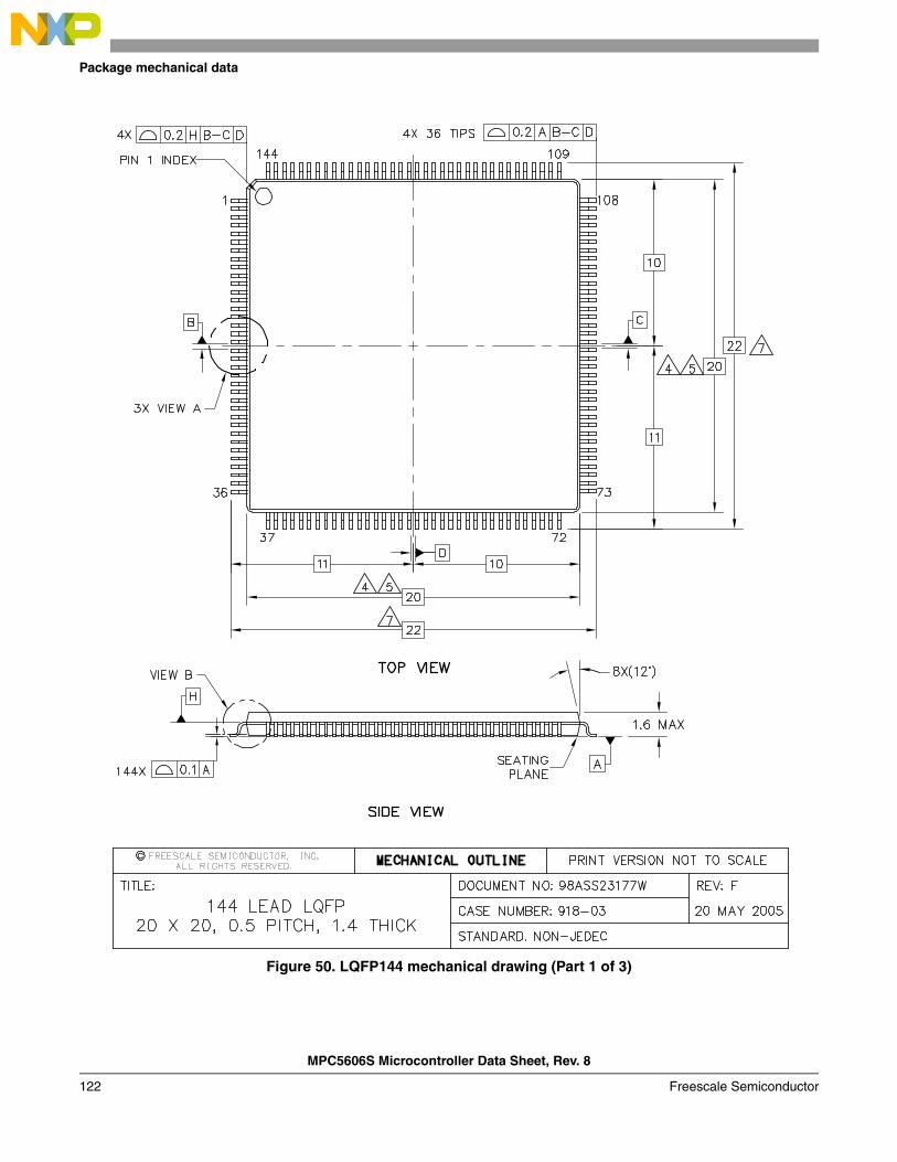
MPC5606S Microcontroller Data Sheet, Rev. 8
Package mechanical data
Freescale Semiconductor122
Figure 50. LQFP144 mechanical drawing (Part 1 of 3)
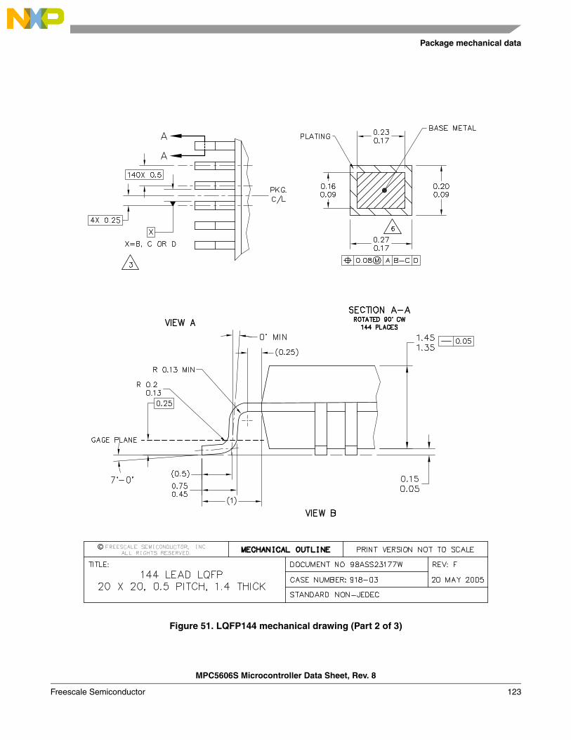
Package mechanical data
MPC5606S Microcontroller Data Sheet, Rev. 8
Freescale Semiconductor 123
Figure 51. LQFP144 mechanical drawing (Part 2 of 3)
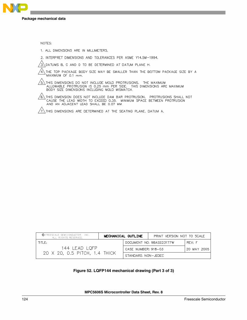
MPC5606S Microcontroller Data Sheet, Rev. 8
Package mechanical data
Freescale Semiconductor124
Figure 52. LQFP144 mechanical drawing (Part 3 of 3)
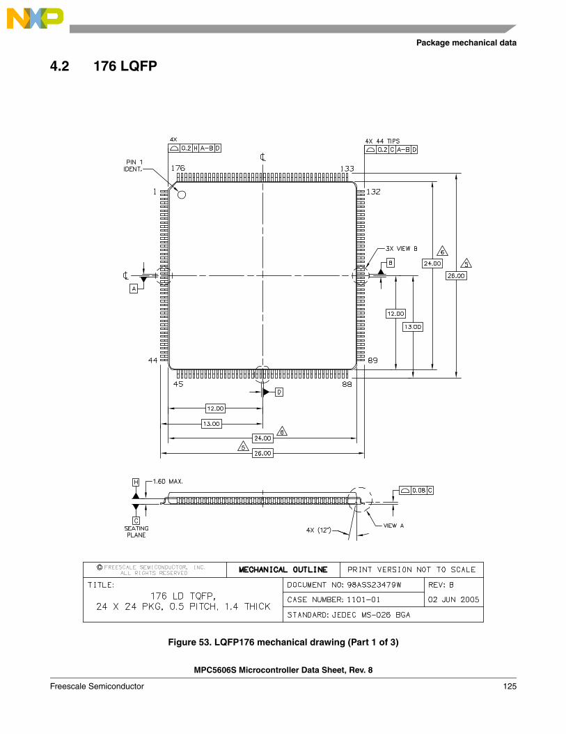
Package mechanical data
MPC5606S Microcontroller Data Sheet, Rev. 8
Freescale Semiconductor 125
4.2 176 LQFP
Figure 53. LQFP176 mechanical drawing (Part 1 of 3)
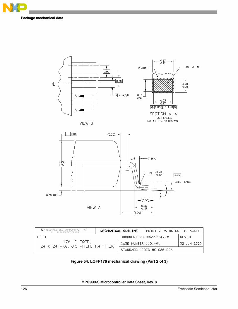
MPC5606S Microcontroller Data Sheet, Rev. 8
Package mechanical data
Freescale Semiconductor126
Figure 54. LQFP176 mechanical drawing (Part 2 of 3)
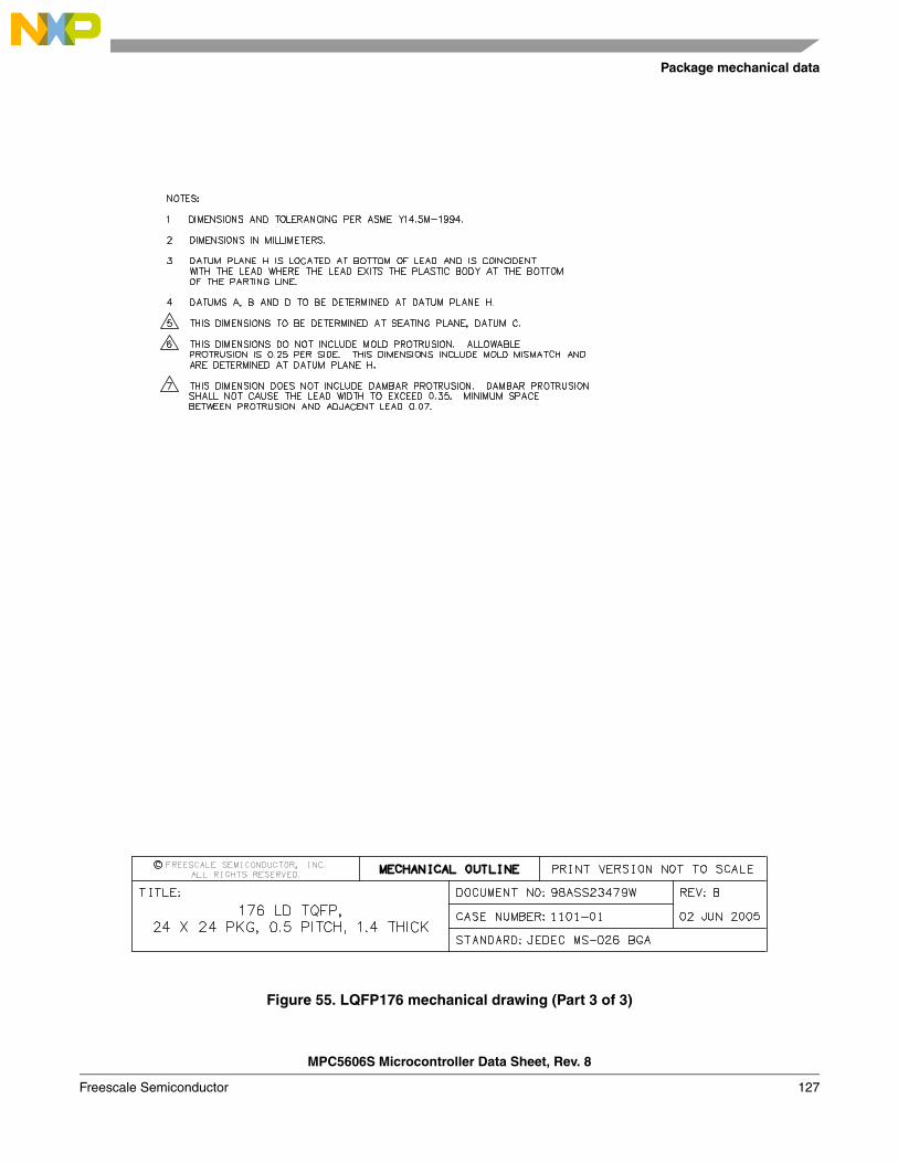
Package mechanical data
MPC5606S Microcontroller Data Sheet, Rev. 8
Freescale Semiconductor 127
Figure 55. LQFP176 mechanical drawing (Part 3 of 3)
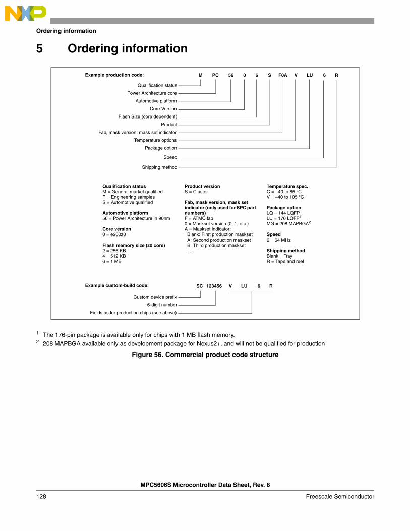
MPC5606S Microcontroller Data Sheet, Rev. 8
Ordering information
Freescale Semiconductor128
5 Ordering information
1 The 176-pin package is available only for chips with 1 MB flash memory.2 208 MAPBGA available only as development package for Nexus2+, and will not be qualified for production
Figure 56. Commercial product code structure
Qualification status
Power Architecture core
Automotive platform
Core Version
Flash Size (core dependent)
Product
Fab, mask version, mask set indicator
M PC 56 S F0A V LUExample production code: 0 6
Temperature options
Package option
Qualification statusM = General market qualifiedP = Engineering samplesS = Automotive qualified
Automotive platform56 = Power Architecture in 90nm
Core version0 = e200z0
Flash memory size (z0 core)2 = 256 KB4 = 512 KB6 = 1 MB
Product versionS = Cluster
Fab, mask version, mask set indicator (only used for SPC part numbers)F = ATMC fab0 = Maskset version (0, 1, etc.)A = Maskset indicator:Blank: First production masksetA: Second production masksetB: Third production maskset...
Shipping method
R
Temperature spec.C = –40 to 85 °CV = –40 to 105 °C
Package optionLQ = 144 LQFPLU = 176 LQFP1
MG = 208 MAPBGA2
Speed6 = 64 MHz
Shipping methodBlank = TrayR = Tape and reel
Speed
6
Example custom-build code: SC 123456 V LU R6
Custom device prefix
6-digit number
Fields as for production chips (see above)
Revision history
MPC5606S Microcontroller Data Sheet, Rev. 8
Freescale Semiconductor 129
6 Revision history
Table 66. Document revision history
Revision Date Substantive changes
1 10-2008 Initial release.
2 18 Aug 2009 Editorial changes and improvements.Harmonized oscillator naming throughout documentFeatures: Updated description of ADC channelsTable 2: Changed max number of GPIOs from 132 to 133 for LQFP176Table 3: Corrected “Peripheral interrupt timer (PIT)” to “Periodic interrupt timer (PIT)”Figure 2:– Added GPIOs to pin function names– Changed function of pin 32: was NC—is VREG_BYPASS– Pin 55: Changed XTAL32 to OSC32K_XTAL– Pin 56: Changed EXTAL32 to OSC32K_EXTALFigure 5:– Added GPIOs to pin function names– Changed function of pin 32: was NC—is VREG_BYPASS– Pin 71: Changed XTAL32 to OSC32K_XTAL– Pin 72: Changed EXTAL32 to OSC32K_EXTALTable 6:– Removed pins EXTAL32, XTAL32 and NMI– Updated VRC_CTL I/O direction and pad typeTable 7:– Replaced “A” with “I” in pad type column– Modified table footnote 3 to replace pad type “A” definition with pad type “I” definitionTable 8: Moved MA[0:2] to follow AN[0:15]Added Section 3.2, “Parameter classification and added classification tags to electrical
characteristics tables where appropriateAdded Section 3.3, “NVUSRO registerTable 14: Removed ESDHBMTable 17: Merged 144- and 176-pin LQFP characteristics into single tableAdded Section 3.6, “Electromagnetic compatibility (EMC) characteristicsTable 26: Removed “TA = 25 °C, after trimming” from conditions for VPORH, VLVDH3V and
VLVDH5VTable 27:– Changed TA = –40 to 125 °C to TA = –40 to 105 °C in note 1– Added STANDBY1 and STANDBY2 mode current characteristicsFigure 14: Updated to reference GPDI register and values for bit PDISection 3.8.1, “I/O pad types: Corrected “four main I/O pad types” to read “three main
I/O pad types”Section 3.8.3, “I/O output DC characteristics: Replaced ipp_hve with PAD3V5V
MPC5606S Microcontroller Data Sheet, Rev. 8
Revision history
Freescale Semiconductor130
2(continued)
18 Aug 2009(continued)
Table 37:– IRMSMED: Replaced SLOW with MEDIUM in parameter column– IRMSFST: Replaced SLOW with FAST in parameter columnSection 3.8.4, “I/O pad current specification: Replaced ipp_hve with PAD3V5VSection 3.10, “RESET electrical characteristics: Replaced ipp_hve with PAD3V5VUpdated Figure 15Updated Figure 18Updated Figure 20Section 3.19, “Pad AC specifications: Replaced IPP_HVE with PAD3V5VTable 45: Added rows IFIRCSTOP and tFIRCSUTable 46:– Added rows tSIRCSU and SIRCTRIM– Updated conditions for SIRCVARAdded Table 42 “ADC input leakage current”Table 50: Updated TUEp and TUEx
Table 7: Modified PC[0] to PC[9]:– I/O direction: was I, is I/O– pad type: was I, is STable 50: Updated values for ‘Input current injection’Section 3.20.3, “Interface to TFT LCD panels: Modified description of event No. 1 in
sequence for active matrix interface timingTable 57: Removed value for Display pixel clock periodTable 53: Removed duplicated row for part number MPC5604SEMLQSection 2.4.2, “Voltage Supply Pins”: Added preferred power up sequence.Section 2.9, “Port pin summary”: Changed reset configuration on ADC pins.Section 3, “Electrical characteristics: Made updates to data. All data is still considered
preliminary.Section 3.7.1, “Voltage regulator electrical characteristics”: Added lower power voltage
regulator and ultra-low power voltage regulator characteristics.
3 — Not released; no substantive changes between Rev. 2 and Rev. 3.
4 — Not released; no substantive changes between Rev. 3 and Rev. 4.
Table 66. Document revision history
Revision Date Substantive changes
Revision history
MPC5606S Microcontroller Data Sheet, Rev. 8
Freescale Semiconductor 131
5 1 Sep 2010 Editorial changes and improvements.Replaced “validation” with “characterization” throughout.Added an entry for Rev. 3 to this table.In the block diagram, in the SXOSC block, changed “32 kHz” to “32 KHz”.Revised the feature section and added the “Feature details” subsection.Renamed the analog pins (were AN..., are ANS...) throughout.Changed several pin names that contained _A, _B, _C, ... to contain _0, _1, _2, ...
throughout.Changed the PCS and oscillator pin names throughout.Revised the feature section and added the “Feature details” subsection.Deleted the out-of-date “Block summary” section.In the 144-pin pinout: • For pin 122, changed PCS_B1 to PCS1_1. • For pin 123, changed PCS_B0 to PCS0_1.In the “144 LQFP package pinout” section, added pinouts for the chips with 512 KB and
256 KB flash memory.In the 176-pin pinout: • For pin 152, changed PCS_B1 to PCS1_1. • For pin 153, changed PCS_B0 to PCS0_1.Revised the “Pad configuration during reset phases”, “Voltage supply pins”, “Pad types”,
“System pins”, and “Nexus pins” sections.Changed several module names and abbreviations to be consistent with the official
module names and abbreviations.In the “Voltage supply pin descriptions” table, revised the entry for VDD12.In the “Debug pin descriptions” table, changed pad type M to pad type M1.In the “Pad types” section, changed “registers in the device reference manual” to
“registers in the SIUL chapter of the device reference manual”.Changed the name of the port-pin summary section (was “Functional ports A, B, C, D,
E, F, G, H, I, J, K”, is “Port pin summary”).In the “Signal details” section: • Renamed the analog pins (were AN..., are ANS...). • Added “ANS[0:15] connect to ATD channels [32:47]” to the ANS signal description. • Added “The available 8 multiplexed channels connect to ATD channels [64:71]” to the
MA signal description. • Deleted “when high; otherwise low to allow a subframe display for pixels” from the
DCU_DE description. • Changed the description for DCU_TAG, PDI_PCLK, TXD_A, and SSD signals. • Added QuadSPI signals. • Deleted “For valid Pixel Data this is high, otherwise low” from the PDI_DE
description. • Changed several pin names that contained _A, _B, _C, ... to contain _0, _1, _2, ...In the “Port pin summary” table: • Changed the pad type for PC[0]—PC[9] (was S, is J). • Moved the AN[0]—AN[15] entries from the “Function” column to the “Special
function” column. • Moved the OSC32K_EXTAL and OSC32K_XTAL entries from the “Function” column
to the “Special function” column. • Added alternate function names and clarifying footnotes to the PF[11]—PF[14]
entries. • Added new information on pad types (including splitting up the existing M pads into
two categories, M1 and M2). • Added a footnote to the “Special function” column title.
Table 66. Document revision history
Revision Date Substantive changes
MPC5606S Microcontroller Data Sheet, Rev. 8
Revision history
Freescale Semiconductor132
5(continued)
1 Sep 2010(continued)
Added a footnote to the “Pad type description” table.In the “Pad type description” table: • Revised the entry for SMD. • Revised the description for the J and M2 pad types.Revised the entry for VSSPLL in the “Absolute maximum ratings” and “Recommended
operating conditions” table.Changed the max value for VDDPLL (was 1.32 V, is 1.4 V) in several tables.Added the “Connecting power supply pins: What to do and what not to do” section.In the “Recommended operating conditions” table, changed the note to state “Maximum
slew...” instead of “Minimum slew...”.In footnote 2 of the “Recommended operating conditions” table, changed “200 µF
capacitance must be connected between VDDR and VSS12” to “10 µF capacitance must be connected between VDDR and VSS12.”.
In the “Recommended operating conditions” section, added a caution on which voltages must be the same.
In the “Recommended operating conditions (3.3 V)” table: • Revised the footnote affecting VDD12/VSS12 supply capacitances. • Deleted footnote 9. • Deleted the entries for VDDPLL and VDD12.In the “Recommended operating conditions (5.0 V)” table: • Changed the footnote text “200 µF capacitance must be connected between VDDR
and VSS12” to “10 µF capacitance must be connected between VDDR and VSS12” and revised the footnote affecting VDD12/VSS12 supply capacitances.
• Added a specification for TVDD. • Deleted the entries for VDDPLL and VDD12.Revised the “EMC requirements on board” section.Added meaningful values to the “EMI testing specifications” table.In the “ESD absolute maximum ratings” table, added a specification for VESD(MM).Deleted the empty “DC Electrical Characteristics” section.In the “I/O pad types” section, added an entry for SMD pads.Added SMC pad electrical characteristics.Revised the “Voltage regulator electrical characteristics” section.Revised the “Low-power voltage regulator electrical characteristics” table.Revised the “Ultra-low power voltage regulator electrical characteristics” table.Revised the “Low voltage monitor electrical characteristics” table.Added the “Recommended power-up and power-down order” section.Added the “Power-up inrush current profile” section.Added the “HPREG load regulation characteristics” section.Revised the “DC electrical characteristics” table.Replaced all values for “STANDBY mode current”.Revised the “I/O pad types” section.In the “I/O input DC electrical characteristics” table: • Changed the specifications for ILKG (was min = <1 A, is min = –1 A; was
max = —, is max = 1 A). • Added an entry for RON.Revised the “I/O output DC characteristics” section.Revised the “MEDIUM configuration output buffer electrical characteristics” table.Revised the “SMD pad electrical characteristics” table and changed its name (is “SMC
pad...”).In the “SMC pad electrical characteristics” table, changed RDSOH to RDSONH and RDSOL
to RDSONL.Moved the IMAX specification from the “SMC pad electrical characteristics” table to the
“Absolute maximum ratings” table.
Table 66. Document revision history
Revision Date Substantive changes
Revision history
MPC5606S Microcontroller Data Sheet, Rev. 8
Freescale Semiconductor 133
5(continued)
1 Sep 2010(continued)
Added the “SMC pad delays” table.Added the “SSD specifications” section.In the “I/O consumption” table, added a specification for IDDMxAVG.Revised the “Fast external crystal oscillator (4–16 MHz) electrical characteristics” table.In the “Slow external crystal oscillator (32 kHz) electrical characteristics” figure,
changed VOSC32K_XTAL to VSXOSC_XTAL.In footnote 2 of the “FMPLL electrical characteristics” table, changed “fCPU 64 MHz can
be achieved only at up to 105 °C” to “fCPU 64 MHz can be achieved only at temperatures up to 105 °C with a maximum FM depth of 2%”.
In the first “Crystal oscillator and resonator connection scheme” figure: • Swapped “XTAL” and “EXTAL”. • Deleted RP.In the second “Crystal oscillator and resonator connection scheme” figure, deleted RF.Added the “Crystal description” table.In the “Fast internal RC oscillator (16 MHz) electrical characteristics” table: • Changed the conditions for FIRCVAR (was “TA = –25 °C”, is “TA = –40 to 105 °C,
trimmed”), removed the associated footnote, and changed the associated guarantee method (was P, is C).
• Changed the max specification for IFIRCPWD (was 10 A, is 1 A).Added the “Resonator description” table.In the “Fast external crystal oscillator (4 to 16 MHz) electrical characteristics” table,
changed footnote 1 (was “... to 125 C”, is “... to 105 C”).In the “Slow external crystal oscillator” section, changed “32 kHz” to “32 KHz”.In the “Slow external crystal oscillator (32 KHz) electrical characteristics” table, added
a footnote to the start-up timing specification.In the “Slow internal RC oscillator (128 KHz) electrical characteristics” table: • Changed the condition for SIRCVAR (was —, is “Trimmed”) and the associated
guarantee method (was P, is C). • Changed the guarantee method for fSIRC (was P, is C).Revised the “Program and erase specifications” table.In the “Flash memory read access timing” table, changed footnote 1 (was “... to 125 C”,
is “... to 105 C”).Revised the “Flash module life” table.Added flash read access timing characteristics.In the “ADC conversion characteristics” table: • Deleted the entry for TUEp (precision channels are not implemented on this device). • Changed the specification for INL (was min = –1.5 LSB and max = 1.5 LSB, is
min = max = 2.5 LSB). • Revised the entry for IINJ (was ±10 mA, is ±5 mA). • Changed the max specifications for RSW1 (was 3 k, is 1 k) and for RSW2 (was 2
k, is 1 k).Added the “LCD driver electrical characteristics” section.Revised the table titles in the “Pad AC specifications” section.Added the “QuadSPI timing” section.Revised the “JTAG interface timing” table.Revised the “Nexus debug port timing” table.Renamed the “Interface to TFT LCD panels—access level” section (is “Interface to TFT
LCD panels”) and revised the table (title and contents) within it.In the “DSPI timing” table, added a min specification for tCSC (is 20 ns).In the DSPI section, added a note (referring to the “DSPI timing” table) to each timing
diagram.Revised the “Ordering information” section.
Table 66. Document revision history
Revision Date Substantive changes
MPC5606S Microcontroller Data Sheet, Rev. 8
Revision history
Freescale Semiconductor134
6 14 Jan 2011 Editorial changes and improvements.Swapped XTAL and EXTAL pins for the 208-pin BGA package and throughout.In the “Pinout and signal descriptions” section, changed WARNING labels to CAUTION
labels.Updated the “Absolute maximum ratings” and “Recommended operating conditions”
tables.Added footnote reference to Vss12 in “Recommended operating conditions (3.3 V)”
table.Updated the “Connecting power supply pins” section.Removed footnote regarding characterization in the “Thermal characteristics” table.Updated the VDD12/VDDPLL operating voltages in the “Electromagnetic interference”
table.Added typical values and updated the “Voltage regulator electrical characteristics,”
“Low-power voltage regulator electrical characteristics,” and “Ultra-low-power voltage regulator electrical characteristics” tables.
Updated classifications and values in the “Low voltage monitor electrical characteristics” table.
Made major modifications and updates to the “DC electrical characteristics” table.Made major modifications and updates to the “I/O input DC electrical characteristics”
table.Made major modifications and updates to the “I/O pull-up/pull-down DC electrical
characteristics” table.Changed “SMC” pads to “SMD” pads throughout.Made updates to the “SMD pad electrical characteristics” table.Added run current during RESET to the “Reset electrical characteristics” table.Updated the FMPLL jitter (peak to peak) specification in the “FMPLL electrical
characteristics” table.Updated fFIRC and tFIRCSU in the “Fast internal RC oscillator (16 MHz) electrical
characteristics” table.Updated fSIRC and tSIRCSU in the “Slow internal RC oscillator (128 kHz) electrical
characteristics” table.Removed “symmetric” pad type from the “Pad AC specifications (5.0 V, PAD3V5V = 0)”
table.Removed “symmetric” pad type from the “Pad AC specifications (3.3 V, PAD3V5V = 1)”
table.Updated VDD12 post-trimming minimum value in the “Low-power voltage regulator
electrical characteristics” table.Updated VDD12 post-trimming minimum value in the “Ultra-low-power voltage regulator
electrical characteristics” table.Updated VLVDLVCORH maximum value in the “Low voltage monitor electrical
characteristics” table.Updated VLVDLVCORL minimum value in the “Low voltage monitor electrical
characteristics” table.Updated value of VDD12/VDDPLL operating voltages in the “Input DC electrical
characteristics” table.Corrected erroneous value of ILKG (105°C case) in the “Input DC electrical
characteristics” table.
Table 66. Document revision history
Revision Date Substantive changes
Revision history
MPC5606S Microcontroller Data Sheet, Rev. 8
Freescale Semiconductor 135
7 17 Mar 2011 In the “Operating mode summary” table, updated the “Mode switch over” specification for “HALT” to be 200.69 µs.
Changed “Advance Information” to “Technical Data” on the front page.Inserted standalone NOTE regarding RAM data retention when VDD12 is not less than
1.08 V.Added footnote to “SSD electrical characteristics” table that specifies Vdd and Tj.In the “SSD electrical characteristics” table, changed the minimum value of IVREF from
2.5 mA to 1.85 mA.Updated the entire “DSPI timing” table.
8 10 Oct 2011 Changed usages of IO to I/O throughout document.In Voltage supply pins section, removed phrase “or noise free supply” from bullet item. In “Recommended operating conditions (3.3 V)” table, changed VSSR in Footnote 2 to
VSSR. In “Recommended operating conditions (5.0 V)” table, changed VSS12 in Footnote 3 to
VSSR. In “Allowed ballast components” table, added 2SD1000 component and specifications. In “Voltage regulator electrical characteristics” section, added figure “Voltage regulator
capacitance connection.”Added “Low voltage monitor vs. reset” figure to “Low voltage monitor electrical
characteristics” section.Added footnote “LVDLVBKP has same post-trim thresholds as LVDLVCOR” to “Low
voltage monitor electrical characteristics” table.Added SIRCPRE and SIRCTRIM specifications to “Slow internal RC oscillator (128 kHz)
electrical characteristics” table. Added footnote to “ADC conversion characteristics (continued)” table “At 32 MHz the
minimum sampling time must be at least 180 ns.” (PS1844)In QuadSPI section, reformatted QuadSPI output timing diagram, QuadSPI input timing
diagram, and QuadSPI clock profile figures. In Figure “Start-up reset requirements,” changed “RESET” to “VRESET.”In “Low voltage monitor electrical characteristics,” table, changed VLVDLVCORH Max to
1.15V.In “SMD pad electrical characteristics” table, changed VOMATCH “C” characteristic to C. In “Voltage regulator electrical characteristics” table, removed upper limit for post-trim
VDD12 and raised min post-trim VDD12 voltage to 1.15 V.In “Low-power voltage regulator electrical characteristics” table, removed upper limit for
post-trim VDD12 and raised min post-trim VDD12 voltage to 1.15 V.In “Ultra-low-power voltage regulator electrical characteristics” table, removed upper
limit for post-trim VDD12 and raised min post-trim VDD12 voltage to 1.15 V. In “SSD electrical characteristics” table, changed values for VVREF from VDDM/2 – 0.02
and VDDM/2 + 0.02 to VDDM/2 – 0.03 and VDDM/2 + 0.03 Added “Voltage regulator capacitance connection” figure. Reformatted “Debug pin descriptions” table (contents not changed). In “16-Channel eMIOS module channel configuration” table, changed VREG startup for
Standby mode from 50 µs to 250 µs.
Table 66. Document revision history
Revision Date Substantive changes
MPC5606S Microcontroller Data Sheet, Rev. 8
Revision history
Freescale Semiconductor136
How to Reach Us:Home Page:www.freescale.com
E-mail:[email protected]
USA/Europe or Locations Not Listed:Freescale SemiconductorTechnical Information Center, CH3701300 N. Alma School RoadChandler, Arizona 85224+1-800-521-6274 or [email protected]
Europe, Middle East, and Africa:Freescale Halbleiter Deutschland GmbHTechnical Information CenterSchatzbogen 781829 Muenchen, Germany+44 1296 380 456 (English)+46 8 52200080 (English)+49 89 92103 559 (German)+33 1 69 35 48 48 (French)[email protected]
Japan:Freescale Semiconductor Japan Ltd.HeadquartersARCO Tower 15F1-8-1, Shimo-Meguro, Meguro-ku,Tokyo 153-0064Japan0120 191014 or +81 3 5437 [email protected]
Asia/Pacific:Freescale Semiconductor China Ltd.Exchange Building 23FNo. 118 Jianguo RoadChaoyang DistrictBeijing 100022 China +86 10 5879 [email protected]
For Literature Requests Only:Freescale Semiconductor Literature Distribution Center1-800-441-2447 or 303-675-2140Fax: [email protected]
Document Number: MPC5606SRev. 811/2011
Information in this document is provided solely to enable system and software implementers to use Freescale Semiconductor products. There are no express or implied copyright licenses granted hereunder to design or fabricate any integrated circuits or integrated circuits based on the information in this document.
Freescale Semiconductor reserves the right to make changes without further notice to any products herein. Freescale Semiconductor makes no warranty, representation or guarantee regarding the suitability of its products for any particular purpose, nor does Freescale Semiconductor assume any liability arising out of the application or use of any product or circuit, and specifically disclaims any and all liability, including without limitation consequential or incidental damages. “Typical” parameters that may be provided in Freescale Semiconductor data sheets and/or specifications can and do vary in different applications and actual performance may vary over time. All operating parameters, including “Typicals”, must be validated for each customer application by customer’s technical experts. Freescale Semiconductor does not convey any license under its patent rights nor the rights of others. Freescale Semiconductor products are not designed, intended, or authorized for use as components in systems intended for surgical implant into the body, or other applications intended to support or sustain life, or for any other application in which the failure of the Freescale Semiconductor product could create a situation where personal injury or death may occur. Should Buyer purchase or use Freescale Semiconductor products for any such unintended or unauthorized application, Buyer shall indemnify and hold Freescale Semiconductor and its officers, employees, subsidiaries, affiliates, and distributors harmless against all claims, costs, damages, and expenses, and reasonable attorney fees arising out of, directly or indirectly, any claim of personal injury or death associated with such unintended or unauthorized use, even if such claim alleges that Freescale Semiconductor was negligent regarding the design or manufacture of the part.
Freescale™ and the Freescale logo are trademarks of Freescale Semiconductor, Inc. All other product or service names are the property of their respective owners.
© Freescale Semiconductor, Inc. 2008–2011. All rights reserved.