Embed Size (px)
Citation preview
REV. 0
Information furnished by Analog Devices is believed to be accurate andreliable. However, no responsibility is assumed by Analog Devices for itsuse, nor for any infringements of patents or other rights of third parties thatmay result from its use. No license is granted by implication or otherwiseunder any patent or patent rights of Analog Devices.
aADV7196A
One Technology Way, P.O. Box 9106, Norwood, MA 02062-9106, U.S.A.
Tel: 781/329-4700 www.analog.com
Fax: 781/326-8703 © Analog Devices, Inc., 2001
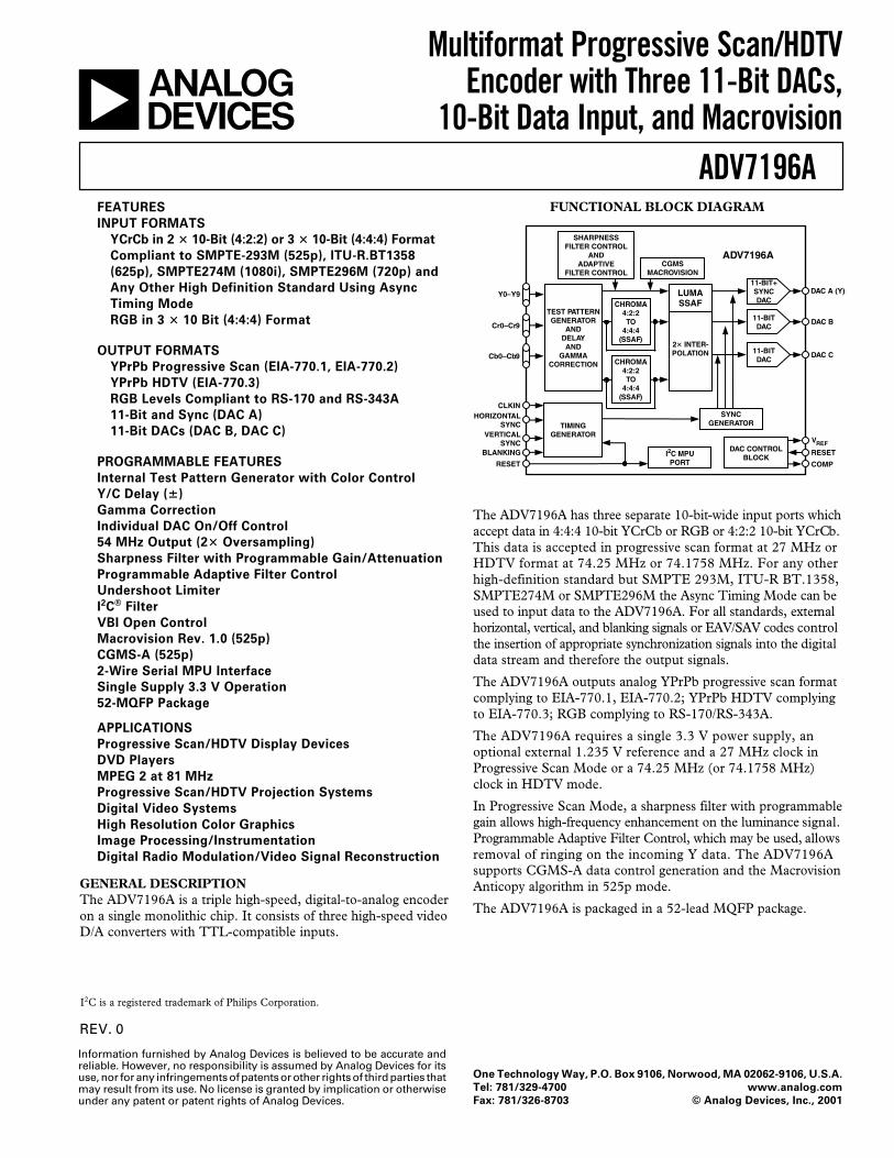
Multiformat Progressive Scan/HDTVEncoder with Three 11-Bit DACs,
10-Bit Data Input, and Macrovision
FUNCTIONAL BLOCK DIAGRAM
CGMSMACROVISION
SHARPNESSFILTER CONTROL
ANDADAPTIVE
FILTER CONTROL
TEST PATTERNGENERATOR
ANDDELAYAND
GAMMACORRECTION
Y0–Y9
Cr0–Cr9
Cb0–Cb9
CHROMA4:2:2TO
4:4:4(SSAF)
2 INTER-POLATION
TIMINGGENERATOR
SYNCGENERATOR
I2C MPUPORT
CLKINHORIZONTAL
SYNCVERTICAL
SYNCBLANKING
RESET
ADV7196A
DAC CONTROLBLOCK
DAC A (Y)
DAC B
DAC C
VREF
RESET
COMP
11-BIT+SYNCDAC
11-BITDAC
11-BITDAC
LUMASSAF
CHROMA4:2:2TO
4:4:4(SSAF)
FEATURES
INPUT FORMATS
YCrCb in 2 10-Bit (4:2:2) or 3 10-Bit (4:4:4) Format
Compliant to SMPTE-293M (525p), ITU-R.BT1358
(625p), SMPTE274M (1080i), SMPTE296M (720p) and
Any Other High Definition Standard Using Async
Timing Mode
RGB in 3 10 Bit (4:4:4) Format
OUTPUT FORMATS
YPrPb Progressive Scan (EIA-770.1, EIA-770.2)
YPrPb HDTV (EIA-770.3)
RGB Levels Compliant to RS-170 and RS-343A
11-Bit and Sync (DAC A)
11-Bit DACs (DAC B, DAC C)
PROGRAMMABLE FEATURES
Internal Test Pattern Generator with Color Control
Y/C Delay ()
Gamma Correction
Individual DAC On/Off Control
54 MHz Output (2 Oversampling)
Sharpness Filter with Programmable Gain/Attenuation
Programmable Adaptive Filter Control
Undershoot Limiter
I2C® Filter
VBI Open Control
Macrovision Rev. 1.0 (525p)
CGMS-A (525p)
2-Wire Serial MPU Interface
Single Supply 3.3 V Operation
52-MQFP Package
APPLICATIONS
Progressive Scan/HDTV Display Devices
DVD Players
MPEG 2 at 81 MHz
Progressive Scan/HDTV Projection Systems
Digital Video Systems
High Resolution Color Graphics
Image Processing/Instrumentation
Digital Radio Modulation/Video Signal Reconstruction
I2C is a registered trademark of Philips Corporation.
GENERAL DESCRIPTIONThe ADV7196A is a triple high-speed, digital-to-analog encoderon a single monolithic chip. It consists of three high-speed videoD/A converters with TTL-compatible inputs.
The ADV7196A has three separate 10-bit-wide input ports whichaccept data in 4:4:4 10-bit YCrCb or RGB or 4:2:2 10-bit YCrCb.This data is accepted in progressive scan format at 27 MHz orHDTV format at 74.25 MHz or 74.1758 MHz. For any otherhigh-definition standard but SMPTE 293M, ITU-R BT.1358,SMPTE274M or SMPTE296M the Async Timing Mode can beused to input data to the ADV7196A. For all standards, externalhorizontal, vertical, and blanking signals or EAV/SAV codes controlthe insertion of appropriate synchronization signals into the digitaldata stream and therefore the output signals.
The ADV7196A outputs analog YPrPb progressive scan formatcomplying to EIA-770.1, EIA-770.2; YPrPb HDTV complyingto EIA-770.3; RGB complying to RS-170/RS-343A.
The ADV7196A requires a single 3.3 V power supply, anoptional external 1.235 V reference and a 27 MHz clock inProgressive Scan Mode or a 74.25 MHz (or 74.1758 MHz)clock in HDTV mode.
In Progressive Scan Mode, a sharpness filter with programmablegain allows high-frequency enhancement on the luminance signal.Programmable Adaptive Filter Control, which may be used, allowsremoval of ringing on the incoming Y data. The ADV7196Asupports CGMS-A data control generation and the MacrovisionAnticopy algorithm in 525p mode.
The ADV7196A is packaged in a 52-lead MQFP package.
REV. 0
ADV7196A
–2–
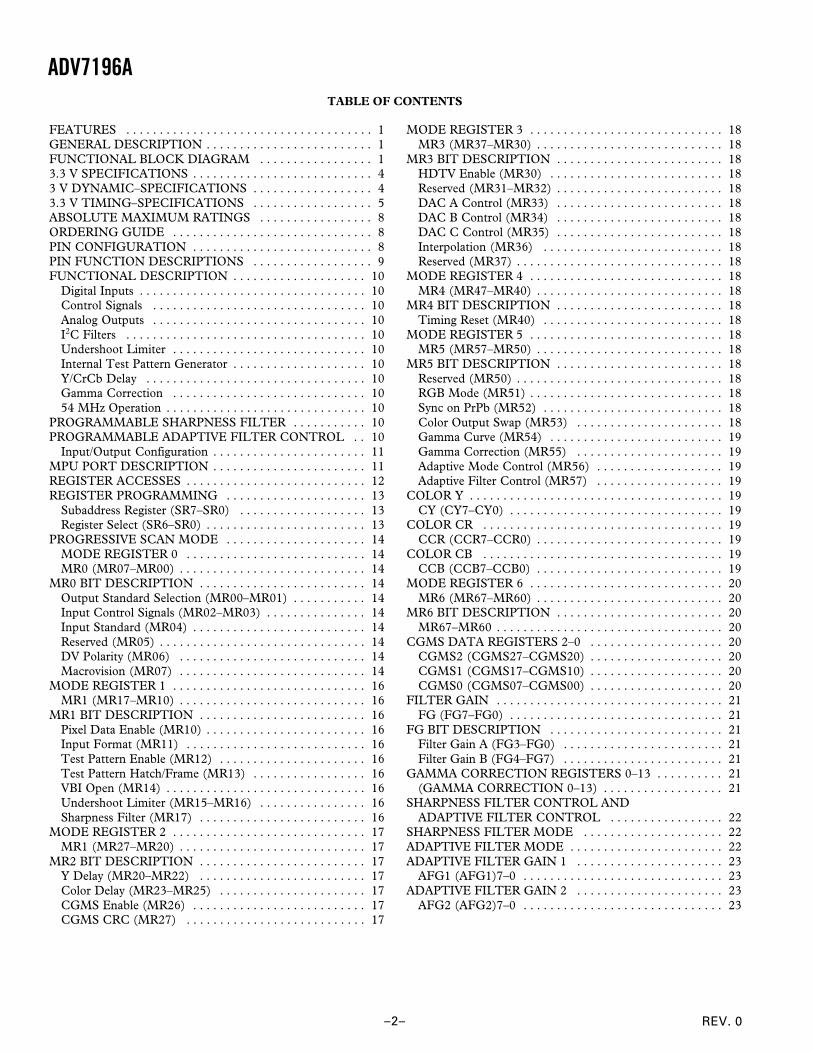
TABLE OF CONTENTS
FEATURES . . . . . . . . . . . . . . . . . . . . . . . . . . . . . . . . . . . . . 1GENERAL DESCRIPTION . . . . . . . . . . . . . . . . . . . . . . . . . 1FUNCTIONAL BLOCK DIAGRAM . . . . . . . . . . . . . . . . . 13.3 V SPECIFICATIONS . . . . . . . . . . . . . . . . . . . . . . . . . . . 43 V DYNAMIC–SPECIFICATIONS . . . . . . . . . . . . . . . . . . 43.3 V TIMING–SPECIFICATIONS . . . . . . . . . . . . . . . . . . 5ABSOLUTE MAXIMUM RATINGS . . . . . . . . . . . . . . . . . 8ORDERING GUIDE . . . . . . . . . . . . . . . . . . . . . . . . . . . . . . 8PIN CONFIGURATION . . . . . . . . . . . . . . . . . . . . . . . . . . . 8PIN FUNCTION DESCRIPTIONS . . . . . . . . . . . . . . . . . . 9FUNCTIONAL DESCRIPTION . . . . . . . . . . . . . . . . . . . . 10
Digital Inputs . . . . . . . . . . . . . . . . . . . . . . . . . . . . . . . . . . 10Control Signals . . . . . . . . . . . . . . . . . . . . . . . . . . . . . . . . 10Analog Outputs . . . . . . . . . . . . . . . . . . . . . . . . . . . . . . . . 10I2C Filters . . . . . . . . . . . . . . . . . . . . . . . . . . . . . . . . . . . . 10Undershoot Limiter . . . . . . . . . . . . . . . . . . . . . . . . . . . . . 10Internal Test Pattern Generator . . . . . . . . . . . . . . . . . . . . 10Y/CrCb Delay . . . . . . . . . . . . . . . . . . . . . . . . . . . . . . . . . 10Gamma Correction . . . . . . . . . . . . . . . . . . . . . . . . . . . . . 1054 MHz Operation . . . . . . . . . . . . . . . . . . . . . . . . . . . . . . 10
PROGRAMMABLE SHARPNESS FILTER . . . . . . . . . . . 10PROGRAMMABLE ADAPTIVE FILTER CONTROL . . 10
Input/Output Configuration . . . . . . . . . . . . . . . . . . . . . . . 11MPU PORT DESCRIPTION . . . . . . . . . . . . . . . . . . . . . . . 11REGISTER ACCESSES . . . . . . . . . . . . . . . . . . . . . . . . . . . 12REGISTER PROGRAMMING . . . . . . . . . . . . . . . . . . . . . 13
Subaddress Register (SR7–SR0) . . . . . . . . . . . . . . . . . . . 13Register Select (SR6–SR0) . . . . . . . . . . . . . . . . . . . . . . . . 13
PROGRESSIVE SCAN MODE . . . . . . . . . . . . . . . . . . . . . 14MODE REGISTER 0 . . . . . . . . . . . . . . . . . . . . . . . . . . . 14MR0 (MR07–MR00) . . . . . . . . . . . . . . . . . . . . . . . . . . . . 14
MR0 BIT DESCRIPTION . . . . . . . . . . . . . . . . . . . . . . . . . 14Output Standard Selection (MR00–MR01) . . . . . . . . . . . 14Input Control Signals (MR02–MR03) . . . . . . . . . . . . . . . 14Input Standard (MR04) . . . . . . . . . . . . . . . . . . . . . . . . . . 14Reserved (MR05) . . . . . . . . . . . . . . . . . . . . . . . . . . . . . . . 14DV Polarity (MR06) . . . . . . . . . . . . . . . . . . . . . . . . . . . . 14Macrovision (MR07) . . . . . . . . . . . . . . . . . . . . . . . . . . . . 14
MODE REGISTER 1 . . . . . . . . . . . . . . . . . . . . . . . . . . . . . 16MR1 (MR17–MR10) . . . . . . . . . . . . . . . . . . . . . . . . . . . . 16
MR1 BIT DESCRIPTION . . . . . . . . . . . . . . . . . . . . . . . . . 16Pixel Data Enable (MR10) . . . . . . . . . . . . . . . . . . . . . . . . 16Input Format (MR11) . . . . . . . . . . . . . . . . . . . . . . . . . . . 16Test Pattern Enable (MR12) . . . . . . . . . . . . . . . . . . . . . . 16Test Pattern Hatch/Frame (MR13) . . . . . . . . . . . . . . . . . 16VBI Open (MR14) . . . . . . . . . . . . . . . . . . . . . . . . . . . . . . 16Undershoot Limiter (MR15–MR16) . . . . . . . . . . . . . . . . 16Sharpness Filter (MR17) . . . . . . . . . . . . . . . . . . . . . . . . . 16
MODE REGISTER 2 . . . . . . . . . . . . . . . . . . . . . . . . . . . . . 17MR1 (MR27–MR20) . . . . . . . . . . . . . . . . . . . . . . . . . . . . 17
MR2 BIT DESCRIPTION . . . . . . . . . . . . . . . . . . . . . . . . . 17Y Delay (MR20–MR22) . . . . . . . . . . . . . . . . . . . . . . . . . 17Color Delay (MR23–MR25) . . . . . . . . . . . . . . . . . . . . . . 17CGMS Enable (MR26) . . . . . . . . . . . . . . . . . . . . . . . . . . 17CGMS CRC (MR27) . . . . . . . . . . . . . . . . . . . . . . . . . . . 17
MODE REGISTER 3 . . . . . . . . . . . . . . . . . . . . . . . . . . . . . 18MR3 (MR37–MR30) . . . . . . . . . . . . . . . . . . . . . . . . . . . . 18
MR3 BIT DESCRIPTION . . . . . . . . . . . . . . . . . . . . . . . . . 18HDTV Enable (MR30) . . . . . . . . . . . . . . . . . . . . . . . . . . 18Reserved (MR31–MR32) . . . . . . . . . . . . . . . . . . . . . . . . . 18DAC A Control (MR33) . . . . . . . . . . . . . . . . . . . . . . . . . 18DAC B Control (MR34) . . . . . . . . . . . . . . . . . . . . . . . . . 18DAC C Control (MR35) . . . . . . . . . . . . . . . . . . . . . . . . . 18Interpolation (MR36) . . . . . . . . . . . . . . . . . . . . . . . . . . . 18Reserved (MR37) . . . . . . . . . . . . . . . . . . . . . . . . . . . . . . . 18
MODE REGISTER 4 . . . . . . . . . . . . . . . . . . . . . . . . . . . . . 18MR4 (MR47–MR40) . . . . . . . . . . . . . . . . . . . . . . . . . . . . 18
MR4 BIT DESCRIPTION . . . . . . . . . . . . . . . . . . . . . . . . . 18Timing Reset (MR40) . . . . . . . . . . . . . . . . . . . . . . . . . . . 18
MODE REGISTER 5 . . . . . . . . . . . . . . . . . . . . . . . . . . . . . 18MR5 (MR57–MR50) . . . . . . . . . . . . . . . . . . . . . . . . . . . . 18
MR5 BIT DESCRIPTION . . . . . . . . . . . . . . . . . . . . . . . . . 18Reserved (MR50) . . . . . . . . . . . . . . . . . . . . . . . . . . . . . . . 18RGB Mode (MR51) . . . . . . . . . . . . . . . . . . . . . . . . . . . . . 18Sync on PrPb (MR52) . . . . . . . . . . . . . . . . . . . . . . . . . . . 18Color Output Swap (MR53) . . . . . . . . . . . . . . . . . . . . . . 18Gamma Curve (MR54) . . . . . . . . . . . . . . . . . . . . . . . . . . 19Gamma Correction (MR55) . . . . . . . . . . . . . . . . . . . . . . 19Adaptive Mode Control (MR56) . . . . . . . . . . . . . . . . . . . 19Adaptive Filter Control (MR57) . . . . . . . . . . . . . . . . . . . 19
COLOR Y . . . . . . . . . . . . . . . . . . . . . . . . . . . . . . . . . . . . . . 19CY (CY7–CY0) . . . . . . . . . . . . . . . . . . . . . . . . . . . . . . . . 19
COLOR CR . . . . . . . . . . . . . . . . . . . . . . . . . . . . . . . . . . . . 19CCR (CCR7–CCR0) . . . . . . . . . . . . . . . . . . . . . . . . . . . . 19
COLOR CB . . . . . . . . . . . . . . . . . . . . . . . . . . . . . . . . . . . . 19CCB (CCB7–CCB0) . . . . . . . . . . . . . . . . . . . . . . . . . . . . 19
MODE REGISTER 6 . . . . . . . . . . . . . . . . . . . . . . . . . . . . . 20MR6 (MR67–MR60) . . . . . . . . . . . . . . . . . . . . . . . . . . . . 20
MR6 BIT DESCRIPTION . . . . . . . . . . . . . . . . . . . . . . . . . 20MR67–MR60 . . . . . . . . . . . . . . . . . . . . . . . . . . . . . . . . . . 20
CGMS DATA REGISTERS 2–0 . . . . . . . . . . . . . . . . . . . . 20CGMS2 (CGMS27–CGMS20) . . . . . . . . . . . . . . . . . . . . 20CGMS1 (CGMS17–CGMS10) . . . . . . . . . . . . . . . . . . . . 20CGMS0 (CGMS07–CGMS00) . . . . . . . . . . . . . . . . . . . . 20
FILTER GAIN . . . . . . . . . . . . . . . . . . . . . . . . . . . . . . . . . . 21FG (FG7–FG0) . . . . . . . . . . . . . . . . . . . . . . . . . . . . . . . . 21
FG BIT DESCRIPTION . . . . . . . . . . . . . . . . . . . . . . . . . . 21Filter Gain A (FG3–FG0) . . . . . . . . . . . . . . . . . . . . . . . . 21Filter Gain B (FG4–FG7) . . . . . . . . . . . . . . . . . . . . . . . . 21
GAMMA CORRECTION REGISTERS 0–13 . . . . . . . . . . 21(GAMMA CORRECTION 0–13) . . . . . . . . . . . . . . . . . . 21
SHARPNESS FILTER CONTROL ANDADAPTIVE FILTER CONTROL . . . . . . . . . . . . . . . . . 22
SHARPNESS FILTER MODE . . . . . . . . . . . . . . . . . . . . . 22ADAPTIVE FILTER MODE . . . . . . . . . . . . . . . . . . . . . . . 22ADAPTIVE FILTER GAIN 1 . . . . . . . . . . . . . . . . . . . . . . 23
AFG1 (AFG1)7–0 . . . . . . . . . . . . . . . . . . . . . . . . . . . . . . 23ADAPTIVE FILTER GAIN 2 . . . . . . . . . . . . . . . . . . . . . . 23
AFG2 (AFG2)7–0 . . . . . . . . . . . . . . . . . . . . . . . . . . . . . . 23
REV. 0
ADV7196A
–3–
ADAPTIVE FILTER GAIN 3 . . . . . . . . . . . . . . . . . . . . . . 23AFG3 (AFG3)7–0 . . . . . . . . . . . . . . . . . . . . . . . . . . . . . . 23
ADAPTIVE FILTER THRESHOLD A . . . . . . . . . . . . . . . 23AFTA (AFTA)7–0 . . . . . . . . . . . . . . . . . . . . . . . . . . . . . . 23
ADAPTIVE FILTER THRESHOLD B . . . . . . . . . . . . . . . 23AFTB (AFTB)7–0 . . . . . . . . . . . . . . . . . . . . . . . . . . . . . . 23
ADAPTIVE FILTER THRESHOLD C . . . . . . . . . . . . . . . 23AFTC (AFTC)7–0 . . . . . . . . . . . . . . . . . . . . . . . . . . . . . 23
SHARPNESS FILTER AND ADAPTIVE FILTERAPPLICATION EXAMPLES . . . . . . . . . . . . . . . . . . . . . 24Sharpness Filter Application . . . . . . . . . . . . . . . . . . . . . . 24Adaptive Filter Control Application . . . . . . . . . . . . . . . . . 25
HDTV MODE . . . . . . . . . . . . . . . . . . . . . . . . . . . . . . . . . . 26MODE REGISTER 0 . . . . . . . . . . . . . . . . . . . . . . . . . . . . . 26
MR0 (MR07–MR00) . . . . . . . . . . . . . . . . . . . . . . . . . . . . 26HEXMR0 BIT DESCRIPTION . . . . . . . . . . . . . . . . . . . . . 26
Output Standard Selection (MR00–MR01) . . . . . . . . . . . 26Input Control Signals (MR02–MR03) . . . . . . . . . . . . . . . 26Reserved (MR04) . . . . . . . . . . . . . . . . . . . . . . . . . . . . . . . 26Input Standard (MR05) . . . . . . . . . . . . . . . . . . . . . . . . . . 26DV Polarity (MR06) . . . . . . . . . . . . . . . . . . . . . . . . . . . . 26Reserved (MR07) . . . . . . . . . . . . . . . . . . . . . . . . . . . . . . . 26
MODE REGISTER 1 . . . . . . . . . . . . . . . . . . . . . . . . . . . . . 27MR1 (MR17–MR10) . . . . . . . . . . . . . . . . . . . . . . . . . . . . 27
MR1 BIT DESCRIPTION . . . . . . . . . . . . . . . . . . . . . . . . . 27Pixel Data Enable (MR10) . . . . . . . . . . . . . . . . . . . . . . . . 27Input Format (MR11) . . . . . . . . . . . . . . . . . . . . . . . . . . . 27Test Pattern Enable (MR12) . . . . . . . . . . . . . . . . . . . . . . 27Test Pattern Hatch/Frame (MR13) . . . . . . . . . . . . . . . . . 27VBI Open (MR14) . . . . . . . . . . . . . . . . . . . . . . . . . . . . . . 27Reserved (MR15–MR17) . . . . . . . . . . . . . . . . . . . . . . . . . 27
MODE REGISTER 2 . . . . . . . . . . . . . . . . . . . . . . . . . . . . . 28MR1 (MR27–MR20) . . . . . . . . . . . . . . . . . . . . . . . . . . . . 28
MR2 BIT DESCRIPTION . . . . . . . . . . . . . . . . . . . . . . . . . 28Y Delay (MR20–MR22) . . . . . . . . . . . . . . . . . . . . . . . . . 28
Color Delay (MR23–MR25) . . . . . . . . . . . . . . . . . . . . . . 28Reserved (MR26–MR27) . . . . . . . . . . . . . . . . . . . . . . . . . 28
MODE REGISTER 3 . . . . . . . . . . . . . . . . . . . . . . . . . . . . . 28MR3 (MR37–MR30) . . . . . . . . . . . . . . . . . . . . . . . . . . . . . 28MR3 BIT DESCRIPTION . . . . . . . . . . . . . . . . . . . . . . . . . 28
HDTV Enable (MR30) . . . . . . . . . . . . . . . . . . . . . . . . . . 28Reserved (MR31–MR32) . . . . . . . . . . . . . . . . . . . . . . . . . 28DAC A Control (MR33) . . . . . . . . . . . . . . . . . . . . . . . . . 28DAC B Control (MR34) . . . . . . . . . . . . . . . . . . . . . . . . . 28DAC C Control (MR35) . . . . . . . . . . . . . . . . . . . . . . . . . 28Reserved (MR36–MR37) . . . . . . . . . . . . . . . . . . . . . . . . . 28
MODE REGISTER 4 . . . . . . . . . . . . . . . . . . . . . . . . . . . . . 29MR4 (MR47–MR40) . . . . . . . . . . . . . . . . . . . . . . . . . . . . 29
MR4 BIT DESCRIPTION . . . . . . . . . . . . . . . . . . . . . . . . . 29Timing Reset (MR40) . . . . . . . . . . . . . . . . . . . . . . . . . . . 29
MODE REGISTER 5 . . . . . . . . . . . . . . . . . . . . . . . . . . . . . 29MR5 (MR57–MR50) . . . . . . . . . . . . . . . . . . . . . . . . . . . . 29
MR5 BIT DESCRIPTION . . . . . . . . . . . . . . . . . . . . . . . . . 29Reserved (MR50) . . . . . . . . . . . . . . . . . . . . . . . . . . . . . . . 29RGB Mode (MR51) . . . . . . . . . . . . . . . . . . . . . . . . . . . . . 29Sync on PrPb (MR52) . . . . . . . . . . . . . . . . . . . . . . . . . . . 29Color Output Swap (MR53) . . . . . . . . . . . . . . . . . . . . . . 29Reserved (MR54–MR57) . . . . . . . . . . . . . . . . . . . . . . . . . 29
DAC TERMINATION AND LAYOUTCONSIDERATIONS . . . . . . . . . . . . . . . . . . . . . . . . . . . 30Voltage Reference . . . . . . . . . . . . . . . . . . . . . . . . . . . . . . 30
PC BOARD LAYOUT CONSIDERATIONS . . . . . . . . . . 30Supply Decoupling . . . . . . . . . . . . . . . . . . . . . . . . . . . . . . 31Digital Signal Interconnect . . . . . . . . . . . . . . . . . . . . . . . . 31Analog Signal Interconnect . . . . . . . . . . . . . . . . . . . . . . . 31Video Output Buffer and Optional Output Filter . . . . . . . 31
OUTLINE DIMENSIONS . . . . . . . . . . . . . . . . . . . . . . . . . 36
REV. 0–4–
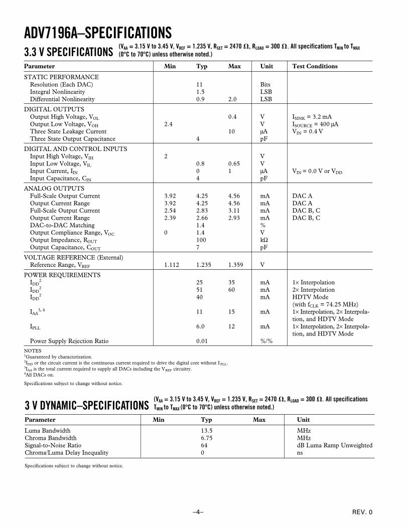
ADV7196A–SPECIFICATIONS3.3 V SPECIFICATIONSParameter Min Typ Max Unit Test Conditions
STATIC PERFORMANCEResolution (Each DAC) 11 BitsIntegral Nonlinearity 1.5 LSBDifferential Nonlinearity 0.9 2.0 LSB
DIGITAL OUTPUTSOutput High Voltage, VOL 0.4 V ISINK = 3.2 mAOutput Low Voltage, VOH 2.4 V ISOURCE = 400 µAThree State Leakage Current 10 µA VIN = 0.4 VThree State Output Capacitance 4 pF
DIGITAL AND CONTROL INPUTSInput High Voltage, VIH 2 VInput Low Voltage, VIL 0.8 0.65 VInput Current, IIN 0 1 µA VIN = 0.0 V or VDD
Input Capacitance, CIN 4 pF
ANALOG OUTPUTSFull-Scale Output Current 3.92 4.25 4.56 mA DAC AOutput Current Range 3.92 4.25 4.56 mA DAC AFull-Scale Output Current 2.54 2.83 3.11 mA DAC B, COutput Current Range 2.39 2.66 2.93 mA DAC B, CDAC-to-DAC Matching 1.4 %Output Compliance Range, VOC 0 1.4 VOutput Impedance, ROUT 100 kΩOutput Capacitance, COUT 7 pF
VOLTAGE REFERENCE (External)Reference Range, VREF 1.112 1.235 1.359 V
POWER REQUIREMENTSIDD
2 25 35 mA 1× InterpolationIDD
2 51 60 mA 2× InterpolationIDD
2 40 mA HDTV Mode(with fCLK = 74.25 MHz)
IAA3, 4 11 15 mA 1× Interpolation, 2× Interpola-
tion, and HDTV ModeIPLL 6.0 12 mA 1× Interpolation, 2× Interpola-
tion, and HDTV ModePower Supply Rejection Ratio 0.01 %/%
NOTES1Guaranteed by characterization.2IDD or the circuit current is the continuous current required to drive the digital core without I PLL.3IAA is the total current required to supply all DACs including the VREF circuitry.4All DACs on.
Specifications subject to change without notice.
(VAA = 3.15 V to 3.45 V, VREF = 1.235 V, RSET = 2470 , RLOAD = 300 . All specifications TMIN to TMAX
(0C to 70C) unless otherwise noted.)
3 V DYNAMIC–SPECIFICATIONSParameter Min Typ Max Unit
Luma Bandwidth 13.5 MHzChroma Bandwidth 6.75 MHzSignal-to-Noise Ratio 64 dB Luma Ramp UnweightedChroma/Luma Delay Inequality 0 ns
Specifications subject to change without notice.
(VAA = 3.15 V to 3.45 V, VREF = 1.235 V, RSET = 2470 , RLOAD = 300 . All specificationsTMIN to TMAX (0C to 70C) unless otherwise noted.)
REV. 0 –5–
ADV7196A
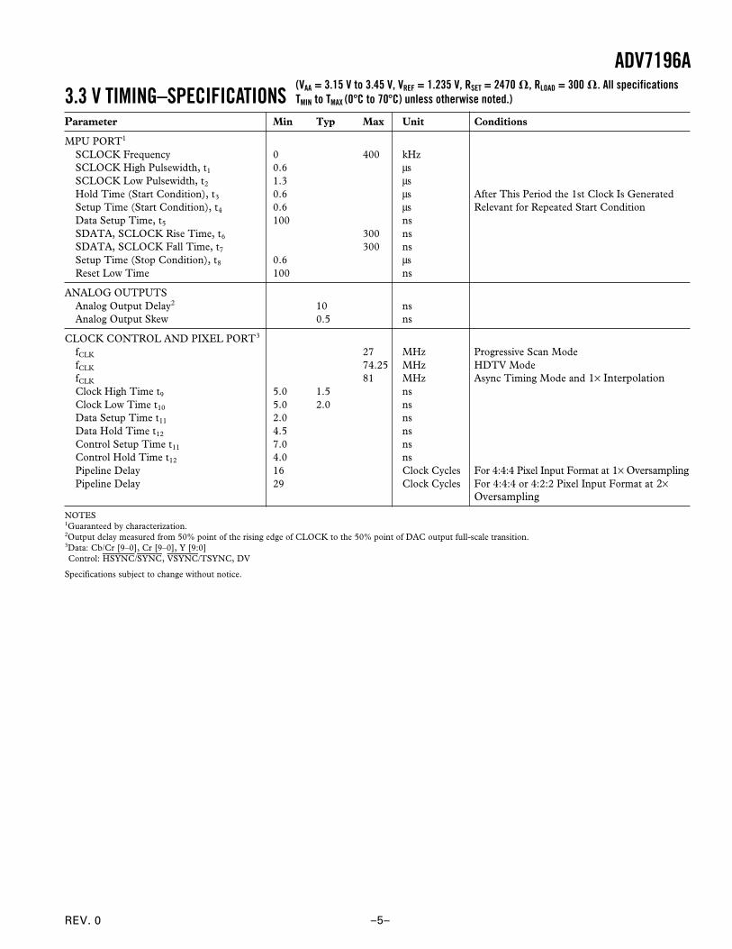
3.3 V TIMING–SPECIFICATIONSParameter Min Typ Max Unit Conditions
MPU PORT1
SCLOCK Frequency 0 400 kHzSCLOCK High Pulsewidth, t1 0.6 µsSCLOCK Low Pulsewidth, t2 1.3 µsHold Time (Start Condition), t3 0.6 µs After This Period the 1st Clock Is GeneratedSetup Time (Start Condition), t4 0.6 µs Relevant for Repeated Start ConditionData Setup Time, t5 100 nsSDATA, SCLOCK Rise Time, t6 300 nsSDATA, SCLOCK Fall Time, t7 300 nsSetup Time (Stop Condition), t8 0.6 µsReset Low Time 100 ns
ANALOG OUTPUTSAnalog Output Delay2 10 nsAnalog Output Skew 0.5 ns
CLOCK CONTROL AND PIXEL PORT3
fCLK 27 MHz Progressive Scan ModefCLK 74.25 MHz HDTV ModefCLK 81 MHz Async Timing Mode and 1× InterpolationClock High Time t9 5.0 1.5 nsClock Low Time t10 5.0 2.0 nsData Setup Time t11 2.0 nsData Hold Time t12 4.5 nsControl Setup Time t11 7.0 nsControl Hold Time t12 4.0 nsPipeline Delay 16 Clock Cycles For 4:4:4 Pixel Input Format at 1× OversamplingPipeline Delay 29 Clock Cycles For 4:4:4 or 4:2:2 Pixel Input Format at 2×
Oversampling
NOTES1Guaranteed by characterization.2Output delay measured from 50% point of the rising edge of CLOCK to the 50% point of DAC output full-scale transition.3Data: Cb/Cr [9–0], Cr [9–0], Y [9:0]Control: HSYNC/SYNC, VSYNC/TSYNC, DV
Specifications subject to change without notice.
(VAA = 3.15 V to 3.45 V, VREF = 1.235 V, RSET = 2470 , RLOAD = 300 . All specificationsTMIN to TMAX (0C to 70C) unless otherwise noted.)
REV. 0
ADV7196A
–6–
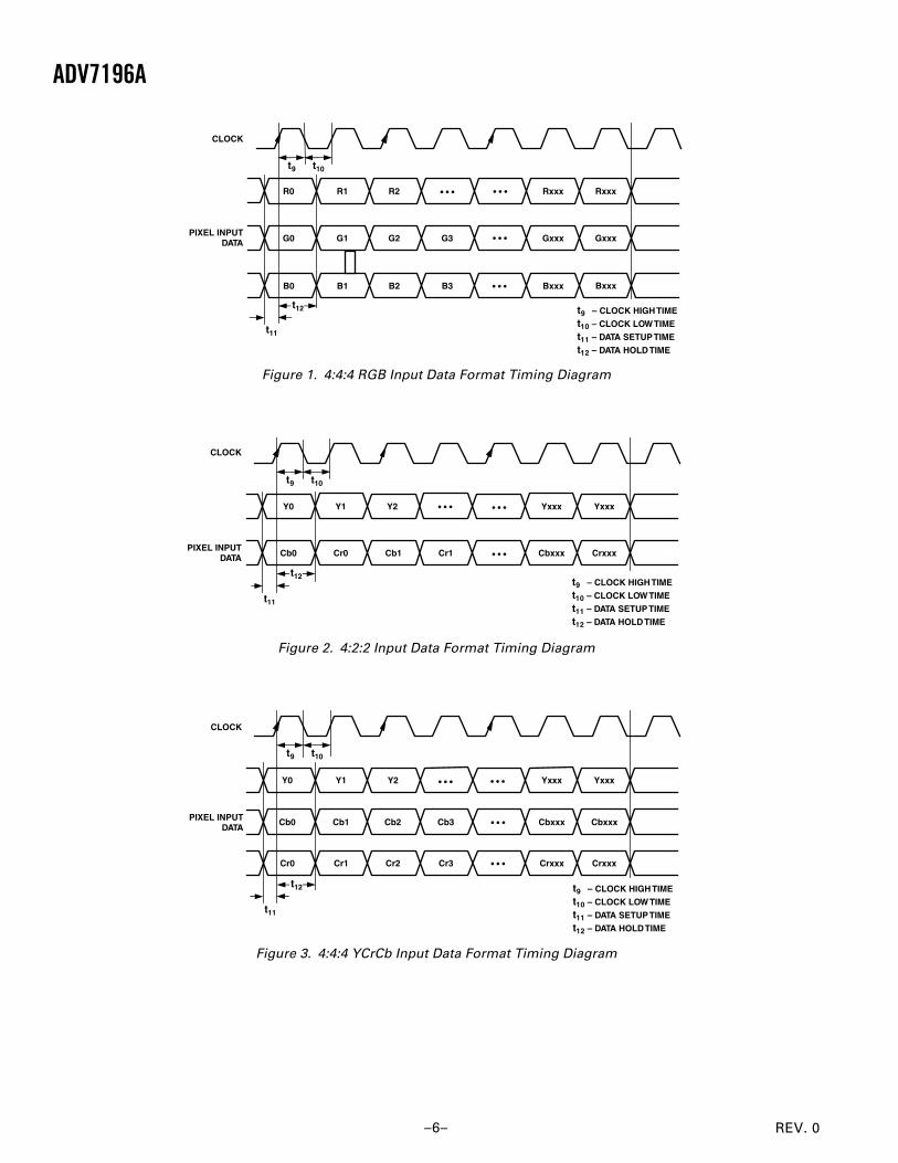
B0 B1 B2 B3 Bxxx Bxxx
CLOCK
PIXEL INPUTDATA
R0
G0
R1
G1
R2
G2 G3
Rxxx
Gxxx
Rxxx
Gxxx
t11
t12
t9 t10
t9 – CLOCK HIGH TIME
t10 – CLOCK LOW TIME
t11 – DATA SETUP TIME
t12 – DATA HOLD TIME
• • • • • •
• • •
• • •
Figure 1. 4:4:4 RGB Input Data Format Timing Diagram
CLOCK
PIXEL INPUTDATA
Y0
Cb0
Y1
Cr0
Y2
Cb1 Cr1
Yxxx
Cbxxx
Yxxx
Crxxx
t11
t12
t9 t10
t9 – CLOCK HIGH TIME
t10 – CLOCK LOW TIME
t11 – DATA SETUP TIME
t12 – DATA HOLD TIME
• • •
• • • • • •
Figure 2. 4:2:2 Input Data Format Timing Diagram
Cr0 Cr1 Cr2 Cr3 Crxxx
CLOCK
PIXEL INPUTDATA
Y0
Cb0
Y1
Cb1
Y2
Cb2 Cb3
Yxxx
Cbxxx
Yxxx
Cbxxx
t11
t12
t9 t10
Crxxx
t9 – CLOCK HIGH TIME
t10 – CLOCK LOW TIME
t11 – DATA SETUP TIME
t12 – DATA HOLD TIME
• • •
• • •
• • •• • •
Figure 3. 4:4:4 YCrCb Input Data Format Timing Diagram
REV. 0
ADV7196A
–7–
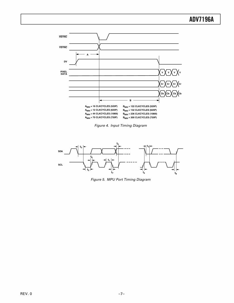
AMIN = 16 CLKCYCLES (525P)
AMIN = 12 CLKCYCLES (625P)
AMIN = 44 CLKCYCLES (1080I)
AMIN = 70 CLKCYCLES (720P)
PIXELDATA
DV
VSYNC
HSYNC
Y Y Y Y
Cr Cr Cr Cr
Cb Cb Cb Cb
B
A
BMIN = 122 CLKCYCLES (525P)
BMIN = 132 CLKCYCLES (625P)
BMIN = 236 CLKCYCLES (1080I)
BMIN = 300 CLKCYCLES (720P)
Figure 4. Input Timing Diagram
t3
t2
t6 t1
t7
t3
t4 t8
SDA
SCL
t5
Figure 5. MPU Port Timing Diagram
REV. 0
ADV7196A
–8–
CAUTIONESD (electrostatic discharge) sensitive device. Electrostatic charges as high as 4000 V readilyaccumulate on the human body and test equipment and can discharge without detection. Althoughthe ADV7196A features proprietary ESD protection circuitry, permanent damage may occur ondevices subjected to high-energy electrostatic discharges. Therefore, proper ESD precautions arerecommended to avoid performance degradation or loss of functionality.
WARNING!
ESD SENSITIVE DEVICE
ABSOLUTE MAXIMUM RATINGS1
VAA to GND . . . . . . . . . . . . . . . . . . . . . . . . . . . . . . . . . . . 7 VVoltage on Any Digital Pin . . . . GND – 0.5 V to VAA + 0.5 VAmbient Operating Temperature (TA) . . . . . –40°C to +85°CStorage Temperature (TS) . . . . . . . . . . . . . . –65°C to +150°CInfrared Reflow Soldering (20 secs) . . . . . . . . . . . . . . . 225°CVapor Phase Soldering (1 minute) . . . . . . . . . . . . . . . . 220°CIOUT to GND2 . . . . . . . . . . . . . . . . . . . . . . . . . . . . 0 V to VAA
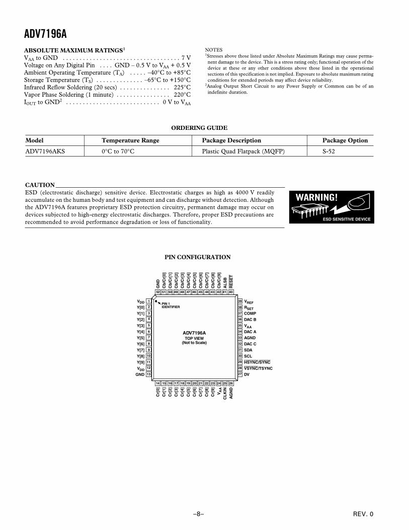
PIN CONFIGURATION
52 51 50 49 48 43 42 41 4047 46 45 44
14 15 16 17 18 19 20 21 22 23 24 25 26
1
2
3
4
5
6
7
8
9
10
11
13
12
PIN 1IDENTIFIER
TOP VIEW(Not to Scale)
39
38
37
36
35
34
33
32
31
30
29
28
27
ADV7196A
Cr[
0]
Cr[
1]
Cr[
2]
Cr[
3]
Cr[
4]
Cr[
5]
Cr[
6]
Cr[
7]
Cr[
8]
Cr[
9]
VA
AC
LK
IN
AG
ND
GN
D
Cb
/Cr[
0]
Cb
/Cr[
1]
Cb
/Cr[
2]
Cb
/Cr[
3]
Cb
/Cr[
4]
Cb
/Cr[
5]
Cb
/Cr[
6]
Cb
/Cr[
7]
Cb
/Cr[
8]
Cb
/Cr[
9]
AL
SB
RE
SE
T
VDD
Y[0]
Y[1]
Y[2]
Y[3]
Y[4]
Y[5]
Y[6]
Y[7]
Y[8]
Y[9]
VDDGND
VREFRSETCOMP
DAC B
VAADAC A
AGND
DAC C
SDA
SCL
HSYNC/SYNC
VSYNC/TSYNC
DV
ORDERING GUIDE
Model Temperature Range Package Description Package Option
ADV7196AKS 0°C to 70°C Plastic Quad Flatpack (MQFP) S-52
NOTES1Stresses above those listed under Absolute Maximum Ratings may cause perma-
nent damage to the device. This is a stress rating only; functional operation of thedevice at these or any other conditions above those listed in the operationalsections of this specification is not implied. Exposure to absolute maximum ratingconditions for extended periods may affect device reliability.
2Analog Output Short Circuit to any Power Supply or Common can be of anindefinite duration.
REV. 0
ADV7196A
–9–
PIN FUNCTION DESCRIPTIONS
Pin Mnemonic Input/Output Function
1, 12 VDD P Digital Power Supply2–11 Y0–Y9 I 10-Bit Progressive Scan/HDTV Input Port for Y Data. Input for G data when
RGB data is input.13, 52 GND G Digital Ground14–23 Cr0–Cr9 I 10-Bit Progressive Scan/HDTV Input Port for Color Data in 4:4:4 Input Mode.
In 4:2:2 mode this input port is not used. Input port for R data when RGB datais input.
24, 35 VAA P Analog Power Supply25 CLKIN I Pixel Clock Input. Requires a 27 MHz reference clock for standard operation in
Progressive Scan Mode or a 74.25 MHz (74.1758 MHz) reference clock inHDTV mode.
26, 33 AGND G Analog Ground27 DV I Video Blanking Control Signal Input28 VSYNC/ I VSYNC, Vertical Sync Control Signal Input or TSYNC Input Control Signal in
TSYNC Async Timing Mode29 HSYNC/ I HSYNC, Horizontal Sync Control Signal Input or SYNC Input Control Signal in
SYNC Async Timing Mode
30 SCL I MPU Port Serial Interface Clock Input31 SDA I/O MPU Port Serial Data Input/Output32 DAC C O Color Component Analog Output of Input Data on Cb/Cr9–0 Input Pins34 DAC A O Y Analog Output36 DAC B O Color Component Analog Output of Input Data on Cr9–Cr0 Input Pins37 COMP O Compensation Pin for DACs. Connect 0.1 µF capacitor from COMP pin to VAA.38 RSET I A 2470 Ω resistor (for input ranges 64–940 and 64–960; output standards
EIA-770.1–EIA-770.3) must be connected from this pin to ground and is used tocontrol the amplitudes of the DAC outputs. For input ranges 0–1023 (outputstandards RS-170, RS-343A) the RSET value must be 2820 Ω.
39 VREF I/O Optional External Voltage Reference Input for DACs or Voltage ReferenceOutput (1.235 V)
40 RESET I This input resets the on-chip timing generator and sets the ADV7196A intoDefault Register setting. Reset is an active low signal.
41 ALSB I TTL Address Input. This signal sets up the LSB of the MPU address. When thispin is tied high, the I2C filter is activated which reduces noise on the I2C interface.When this pin is tied low, the input bandwidth on the I2C interface is increased.
42–51 Cb/Cr9–0 I 10-Bit Progressive Scan/HDTV Input Port for Color Data. In 4:2:2 mode themultiplexed CrCb data must be input on these pins. Input port for B data whenRGB is input.
REV. 0
ADV7196A
–10–
FUNCTIONAL DESCRIPTIONDigital InputsThe digital inputs of the ADV7196A are TTL compatible. 30-bitYCrCb or RGB pixel data in 4:4:4 format or 20-bit YCrCb pixeldata in 4:2:2 format is latched into the device on the rising edgeof each clock cycle at 74.25 MHz or 74.1758 in HDTV mode.It is also possible to input 3 × 10 bit RGB data in 4:4:4 to theADV7196A. It is recommended to input data in 4:2:2 mode tomake use of the Chroma SSAFs on the ADV7196A. As can beseen in the figure below, this filter has a 0 dB pass band responseand prevents signal components being folded back in to the fre-quency band. In 4:4:4: input mode, the video data is alreadyinterpolated by the external input device and the Chroma SSAFsof the ADV7196A are bypassed.
RBW 10kHz VBW 300Hz SWP 17.0SECSTART 100kHz STOP 20.00MHz
RL –10.0dBm 10dB/ 3.18MHzATTEN 10dB VAVG 1 MKR 0dB
Figure 6. ADV7196A SSAF Response to a 2.5 MHz ChromaSweep Using 4:2:2 Input Mode
RBW 10kHz VBW 300Hz SWP 17.0SECSTART 100kHz STOP 20.00MHz
RL –10.0dBm 10dB/ 3.12MHzATTEN 10dB VAVG 4 MKR –3.00dB
Figure 7. Conventional Filter Response to a 2.5 MHz ChromaSweep Using 4:4:4 Input Mode
Control SignalsThe ADV7196A accepts sync control signals accompanied byvalid 4:2:2 or 4:4:4 data. These external horizontal, vertical andblanking pulses (or EAV/SAV codes) control the insertion ofappropriate sync information into the output signals.
Analog OutputsThe analog Y signal is output on the 11-Bit + Sync DAC A,the color component analog signals on the 11-Bit DACs B, Cconforming to EIA-770.1 or EIA-770.2 standards in PS modeor EIA-770.3 in HDTV mode. RSET has a value of 2470 Ω(EIA-770.1, EIA-770.2, EIA-770.3), RLOAD has a value of 300 Ω.For RGB outputs conforming to RS-170/RS-343A output standardsRSET must have a value of 2820 Ω.
I2C FiltersA selectable internal I2C filter allows significant noise reductionon the I2C interface. In setting ALSB high, the input bandwidthon the I2C lines is reduced and pulses of less than 50 ns are notpassed to the I2C controller. Setting ALSB low allows greaterinput bandwidth on the I2C lines.
Undershoot LimiterA limiter can be applied to the Y data before it is applied to the DACs.Available limit values are –1.5 IRE, –6 IRE, –11 IRE below blank-ing. This functionality is available in Progressive Scan mode only.
Internal Test Pattern GeneratorThe ADV7196A can generate a cross-hatch pattern (white linesagainst a black background). Additionally, the ADV7196A canoutput a uniform color pattern. The color of the lines or uniformfield/frame can be programmed by the user.
Y/CrCb DelayThe Y output and the color component outputs can be delayedwrt the falling edge of the horizontal sync signal by up to fourclock cycles.
Gamma CorrectionGamma correction may be performed on the luma data. Theuser has the choice to use either of two different gamma curves,A or B. At any one time one of these curves is operational if gammacorrection is enabled. Gamma correction allows the mapping ofthe luma data to a user-defined function.
54 MHz OperationIn Progressive Scan mode, it is possible to operate the three out-put DACs at 54 MHz or 27 MHz. The ADV7196A is suppliedwith a 27 MHz clock synced with the incoming data. If required, asecond stage interpolation filter interpolates the data to 54 MHzbefore it is applied to the three output DACs. The second stageinterpolation filter is controlled by MR36. After applying aReset it is recommended to toggle this bit. Before toggling this bit,3Ehex must be written to address 09hex.
PROGRAMMABLE SHARPNESS FILTERSharpness Filter Mode is applicable to the Y data only in Progres-sive Scan mode. The desired frequency response can be chosenby the user in programming the correct value via the I2C. Thevariation of frequency responses can be seen in the figures on thefollowing pages.
PROGRAMMABLE ADAPTIVE FILTER CONTROLIf the Adaptive Filter Mode is enabled (Progressive Scan mode only),it is possible to compensate for large edge transitions on theincoming Y data. Sensitivity and attenuation are all program-mable over the I2C. For further information refer to SharpnessFilter Control and Adaptive Filter Control section.
REV. 0
ADV7196A
–11–
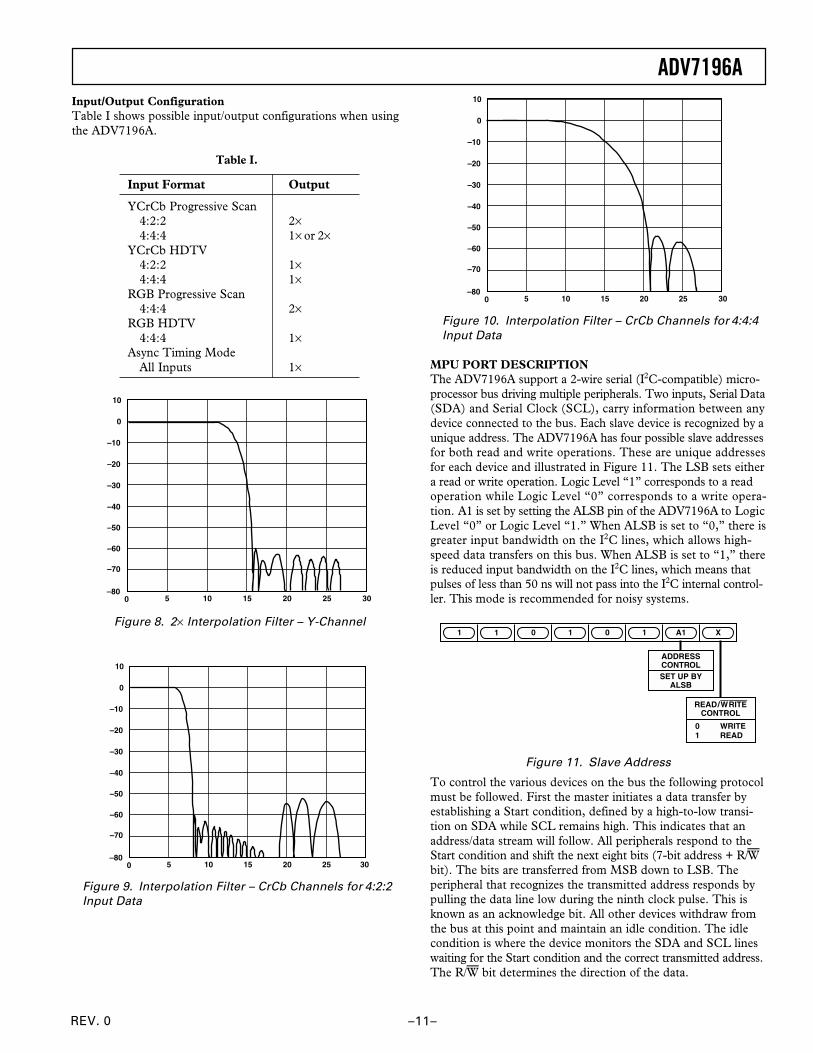
Input/Output ConfigurationTable I shows possible input/output configurations when usingthe ADV7196A.
Table I.
Input Format Output
YCrCb Progressive Scan4:2:2 2×4:4:4 1× or 2×
YCrCb HDTV4:2:2 1×4:4:4 1×
RGB Progressive Scan4:4:4 2×
RGB HDTV4:4:4 1×
Async Timing ModeAll Inputs 1×
10
0
–80
–40
–50
–60
–70
–20
–30
–10
5 10 15 20 250 30
Figure 8. 2× Interpolation Filter – Y-Channel
10
0
–80
–40
–50
–60
–70
–20
–30
–10
5 10 15 20 250 30
Figure 9. Interpolation Filter – CrCb Channels for 4:2:2Input Data
10
0
–80
–40
–50
–60
–70
–20
–30
–10
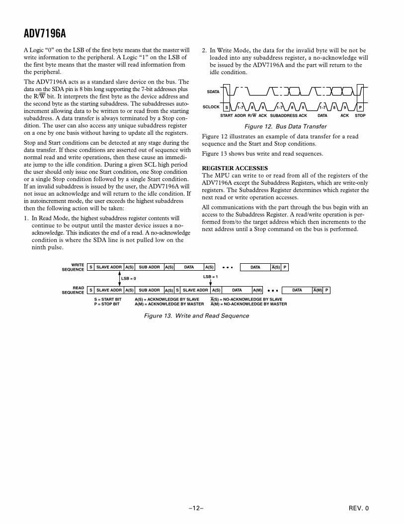
5 10 15 20 250 30
Figure 10. Interpolation Filter – CrCb Channels for 4:4:4Input Data
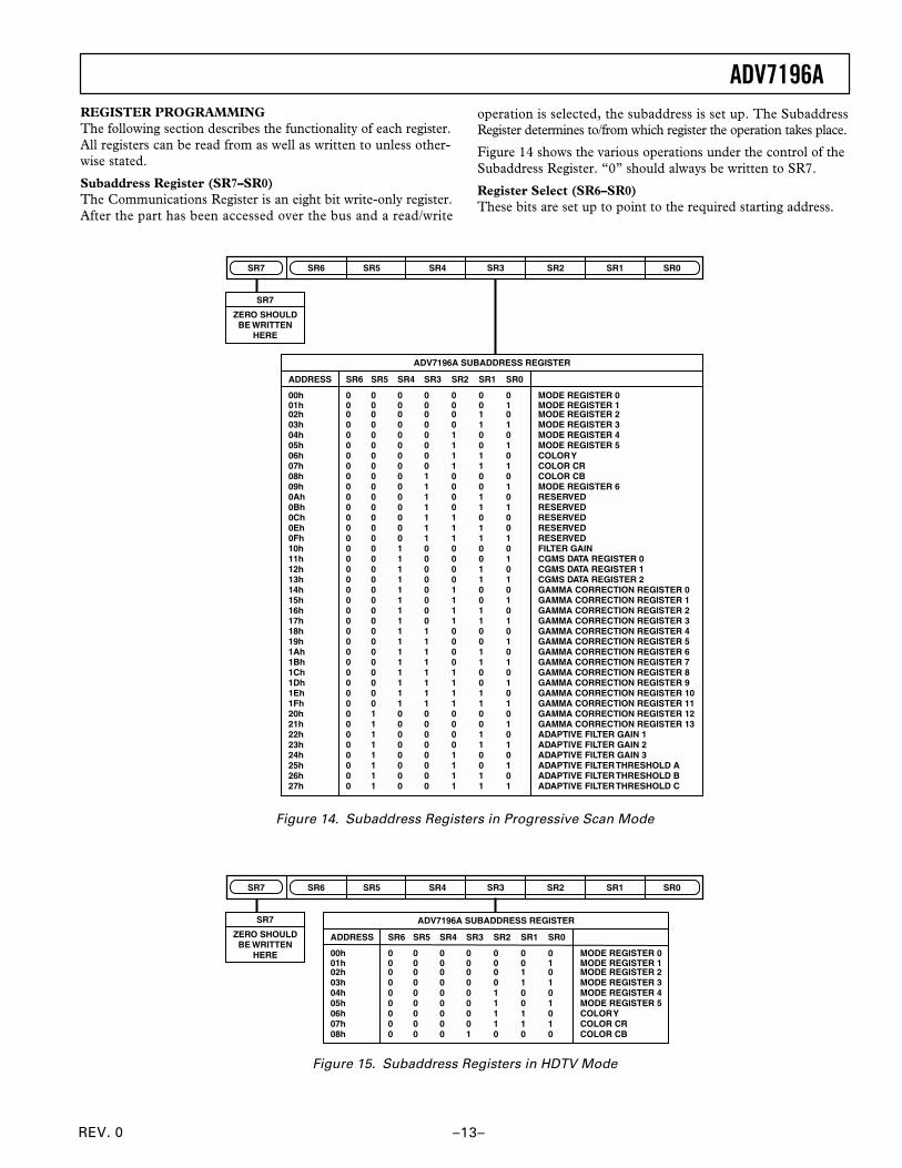
MPU PORT DESCRIPTIONThe ADV7196A support a 2-wire serial (I2C-compatible) micro-processor bus driving multiple peripherals. Two inputs, Serial Data(SDA) and Serial Clock (SCL), carry information between anydevice connected to the bus. Each slave device is recognized by aunique address. The ADV7196A has four possible slave addressesfor both read and write operations. These are unique addressesfor each device and illustrated in Figure 11. The LSB sets eithera read or write operation. Logic Level “1” corresponds to a readoperation while Logic Level “0” corresponds to a write opera-tion. A1 is set by setting the ALSB pin of the ADV7196A to LogicLevel “0” or Logic Level “1.” When ALSB is set to “0,” there isgreater input bandwidth on the I2C lines, which allows high-speed data transfers on this bus. When ALSB is set to “1,” thereis reduced input bandwidth on the I2C lines, which means thatpulses of less than 50 ns will not pass into the I2C internal control-ler. This mode is recommended for noisy systems.
1 X1 0 1 0 1 A1
ADDRESSCONTROLSET UP BY
ALSB
READ/WRITECONTROL
0 WRITE1 READ
Figure 11. Slave Address
To control the various devices on the bus the following protocolmust be followed. First the master initiates a data transfer byestablishing a Start condition, defined by a high-to-low transi-tion on SDA while SCL remains high. This indicates that anaddress/data stream will follow. All peripherals respond to theStart condition and shift the next eight bits (7-bit address + R/Wbit). The bits are transferred from MSB down to LSB. Theperipheral that recognizes the transmitted address responds bypulling the data line low during the ninth clock pulse. This isknown as an acknowledge bit. All other devices withdraw fromthe bus at this point and maintain an idle condition. The idlecondition is where the device monitors the SDA and SCL lineswaiting for the Start condition and the correct transmitted address.The R/W bit determines the direction of the data.
REV. 0
ADV7196A
–12–
A Logic “0” on the LSB of the first byte means that the master willwrite information to the peripheral. A Logic “1” on the LSB ofthe first byte means that the master will read information fromthe peripheral.
The ADV7196A acts as a standard slave device on the bus. Thedata on the SDA pin is 8 bits long supporting the 7-bit addresses plusthe R/W bit. It interprets the first byte as the device address andthe second byte as the starting subaddress. The subaddresses auto-increment allowing data to be written to or read from the startingsubaddress. A data transfer is always terminated by a Stop con-dition. The user can also access any unique subaddress registeron a one by one basis without having to update all the registers.
Stop and Start conditions can be detected at any stage during thedata transfer. If these conditions are asserted out of sequence withnormal read and write operations, then these cause an immedi-ate jump to the idle condition. During a given SCL high periodthe user should only issue one Start condition, one Stop conditionor a single Stop condition followed by a single Start condition.If an invalid subaddress is issued by the user, the ADV7196A willnot issue an acknowledge and will return to the idle condition. Ifin autoincrement mode, the user exceeds the highest subaddressthen the following action will be taken:
1. In Read Mode, the highest subaddress register contents willcontinue to be output until the master device issues a no-acknowledge. This indicates the end of a read. A no-acknowledgecondition is where the SDA line is not pulled low on theninth pulse.
2. In Write Mode, the data for the invalid byte will be not beloaded into any subaddress register, a no-acknowledge willbe issued by the ADV7196A and the part will return to theidle condition.
1–7 8 9 1–7 8 9 1–7 8 9 PS
START ADDR R/W ACK SUBADDRESS ACK DATA ACK STOP
SDATA
SCLOCK
Figure 12. Bus Data Transfer
Figure 12 illustrates an example of data transfer for a readsequence and the Start and Stop conditions.
Figure 13 shows bus write and read sequences.
REGISTER ACCESSESThe MPU can write to or read from all of the registers of theADV7196A except the Subaddress Registers, which are write-onlyregisters. The Subaddress Register determines which register thenext read or write operation accesses.
All communications with the part through the bus begin with anaccess to the Subaddress Register. A read/write operation is per-formed from/to the target address which then increments to thenext address until a Stop command on the bus is performed.
DATA A(S)S SLAVE ADDR A(S) SUB ADDR A(S)
LSB = 0 LSB = 1
DATA A(S) P
S SLAVE ADDR A(S) SUB ADDR A(S) S SLAVE ADDR A(S) DATA A(M) A(M)DATA P
WRITESEQUENCE
READSEQUENCE
S = START BIT A(S) = ACKNOWLEDGE BY SLAVE A(S) = NO-ACKNOWLEDGE BY SLAVEP = STOP BIT A(M) = ACKNOWLEDGE BY MASTER A(M) = NO-ACKNOWLEDGE BY MASTER
Figure 13. Write and Read Sequence
REV. 0
ADV7196A
–13–
REGISTER PROGRAMMINGThe following section describes the functionality of each register.All registers can be read from as well as written to unless other-wise stated.
Subaddress Register (SR7–SR0)The Communications Register is an eight bit write-only register.After the part has been accessed over the bus and a read/write
operation is selected, the subaddress is set up. The SubaddressRegister determines to/from which register the operation takes place.
Figure 14 shows the various operations under the control of theSubaddress Register. “0” should always be written to SR7.
Register Select (SR6–SR0)These bits are set up to point to the required starting address.
SR4 SR3 SR2 SR1 SR0SR7 SR6 SR5
ADDRESS SR6 SR5 SR4 SR3 SR2 SR1 SR0
00h 0 0 0 0 0 0 0 MODE REGISTER 001h 0 0 0 0 0 0 1 MODE REGISTER 102h 0 0 0 0 0 1 0 MODE REGISTER 203h 0 0 0 0 0 1 1 MODE REGISTER 304h 0 0 0 0 1 0 0 MODE REGISTER 405h 0 0 0 0 1 0 1 MODE REGISTER 506h 0 0 0 0 1 1 0 COLOR Y07h 0 0 0 0 1 1 1 COLOR CR08h 0 0 0 1 0 0 0 COLOR CB09h 0 0 0 1 0 0 1 MODE REGISTER 60Ah 0 0 0 1 0 1 0 RESERVED0Bh 0 0 0 1 0 1 1 RESERVED0Ch 0 0 0 1 1 0 0 RESERVED0Eh 0 0 0 1 1 1 0 RESERVED0Fh 0 0 0 1 1 1 1 RESERVED10h 0 0 1 0 0 0 0 FILTER GAIN11h 0 0 1 0 0 0 1 CGMS DATA REGISTER 012h 0 0 1 0 0 1 0 CGMS DATA REGISTER 113h 0 0 1 0 0 1 1 CGMS DATA REGISTER 214h 0 0 1 0 1 0 0 GAMMA CORRECTION REGISTER 015h 0 0 1 0 1 0 1 GAMMA CORRECTION REGISTER 116h 0 0 1 0 1 1 0 GAMMA CORRECTION REGISTER 217h 0 0 1 0 1 1 1 GAMMA CORRECTION REGISTER 318h 0 0 1 1 0 0 0 GAMMA CORRECTION REGISTER 419h 0 0 1 1 0 0 1 GAMMA CORRECTION REGISTER 51Ah 0 0 1 1 0 1 0 GAMMA CORRECTION REGISTER 61Bh 0 0 1 1 0 1 1 GAMMA CORRECTION REGISTER 71Ch 0 0 1 1 1 0 0 GAMMA CORRECTION REGISTER 81Dh 0 0 1 1 1 0 1 GAMMA CORRECTION REGISTER 91Eh 0 0 1 1 1 1 0 GAMMA CORRECTION REGISTER 101Fh 0 0 1 1 1 1 1 GAMMA CORRECTION REGISTER 1120h 0 1 0 0 0 0 0 GAMMA CORRECTION REGISTER 1221h 0 1 0 0 0 0 1 GAMMA CORRECTION REGISTER 1322h 0 1 0 0 0 1 0 ADAPTIVE FILTER GAIN 123h 0 1 0 0 0 1 1 ADAPTIVE FILTER GAIN 224h 0 1 0 0 1 0 0 ADAPTIVE FILTER GAIN 325h 0 1 0 0 1 0 1 ADAPTIVE FILTER THRESHOLD A26h 0 1 0 0 1 1 0 ADAPTIVE FILTER THRESHOLD B27h 0 1 0 0 1 1 1 ADAPTIVE FILTER THRESHOLD C
ADV7196A SUBADDRESS REGISTER
ZERO SHOULDBE WRITTEN
HERE
SR7
Figure 14. Subaddress Registers in Progressive Scan Mode
SR4 SR3 SR2 SR1 SR0SR7 SR6 SR5
ADDRESS SR6 SR5 SR4 SR3 SR2 SR1 SR0
00h 0 0 0 0 0 0 0 MODE REGISTER 001h 0 0 0 0 0 0 1 MODE REGISTER 102h 0 0 0 0 0 1 0 MODE REGISTER 203h 0 0 0 0 0 1 1 MODE REGISTER 304h 0 0 0 0 1 0 0 MODE REGISTER 405h 0 0 0 0 1 0 1 MODE REGISTER 506h 0 0 0 0 1 1 0 COLOR Y07h 0 0 0 0 1 1 1 COLOR CR08h 0 0 0 1 0 0 0 COLOR CB
ADV7196A SUBADDRESS REGISTER
ZERO SHOULDBE WRITTEN
HERE
SR7
Figure 15. Subaddress Registers in HDTV Mode
REV. 0
ADV7196A
–14–
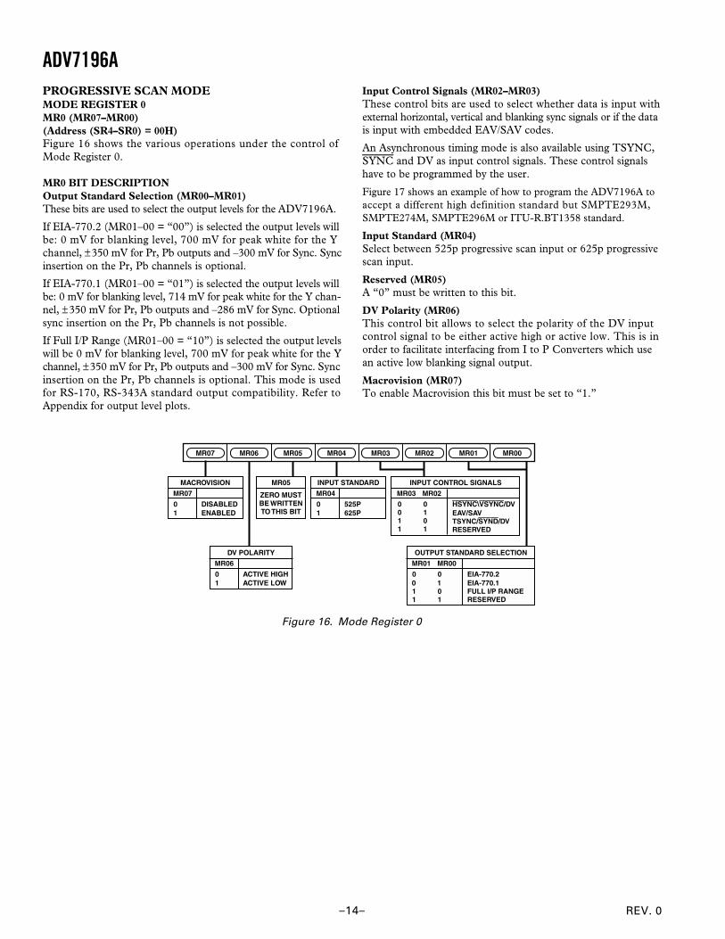
PROGRESSIVE SCAN MODEMODE REGISTER 0MR0 (MR07–MR00)(Address (SR4–SR0) = 00H)Figure 16 shows the various operations under the control ofMode Register 0.
MR0 BIT DESCRIPTIONOutput Standard Selection (MR00–MR01)These bits are used to select the output levels for the ADV7196A.
If EIA-770.2 (MR01–00 = “00”) is selected the output levels willbe: 0 mV for blanking level, 700 mV for peak white for the Ychannel, ±350 mV for Pr, Pb outputs and –300 mV for Sync. Syncinsertion on the Pr, Pb channels is optional.
If EIA-770.1 (MR01–00 = “01”) is selected the output levels willbe: 0 mV for blanking level, 714 mV for peak white for the Y chan-nel, ±350 mV for Pr, Pb outputs and –286 mV for Sync. Optionalsync insertion on the Pr, Pb channels is not possible.
If Full I/P Range (MR01–00 = “10”) is selected the output levelswill be 0 mV for blanking level, 700 mV for peak white for the Ychannel, ±350 mV for Pr, Pb outputs and –300 mV for Sync. Syncinsertion on the Pr, Pb channels is optional. This mode is usedfor RS-170, RS-343A standard output compatibility. Refer toAppendix for output level plots.
Input Control Signals (MR02–MR03)These control bits are used to select whether data is input withexternal horizontal, vertical and blanking sync signals or if the datais input with embedded EAV/SAV codes.
An Asynchronous timing mode is also available using TSYNC,SYNC and DV as input control signals. These control signalshave to be programmed by the user.
Figure 17 shows an example of how to program the ADV7196A toaccept a different high definition standard but SMPTE293M,SMPTE274M, SMPTE296M or ITU-R.BT1358 standard.
Input Standard (MR04)Select between 525p progressive scan input or 625p progressivescan input.
Reserved (MR05)A “0” must be written to this bit.
DV Polarity (MR06)This control bit allows to select the polarity of the DV inputcontrol signal to be either active high or active low. This is inorder to facilitate interfacing from I to P Converters which usean active low blanking signal output.
Macrovision (MR07)To enable Macrovision this bit must be set to “1.”
MR01MR07 MR02MR04MR05MR06
MR07
0 DISABLED1 ENABLED
MACROVISION
MR03 MR00
ZERO MUSTBE WRITTENTO THIS BIT
MR05
MR06
0 ACTIVE HIGH1 ACTIVE LOW
DV POLARITY
MR04
0 525P1 625P
INPUT STANDARD
MR03 MR02
HSYNC\VSYNC/DVEAV/SAVTSYNC/SYND/DVRESERVED
INPUT CONTROL SIGNALS
MR01 MR00
0 0 EIA-770.20 1 EIA-770.11 0 FULL I/P RANGE1 1 RESERVED
OUTPUT STANDARD SELECTION
0101
0011
Figure 16. Mode Register 0
REV. 0
ADV7196A
–15–
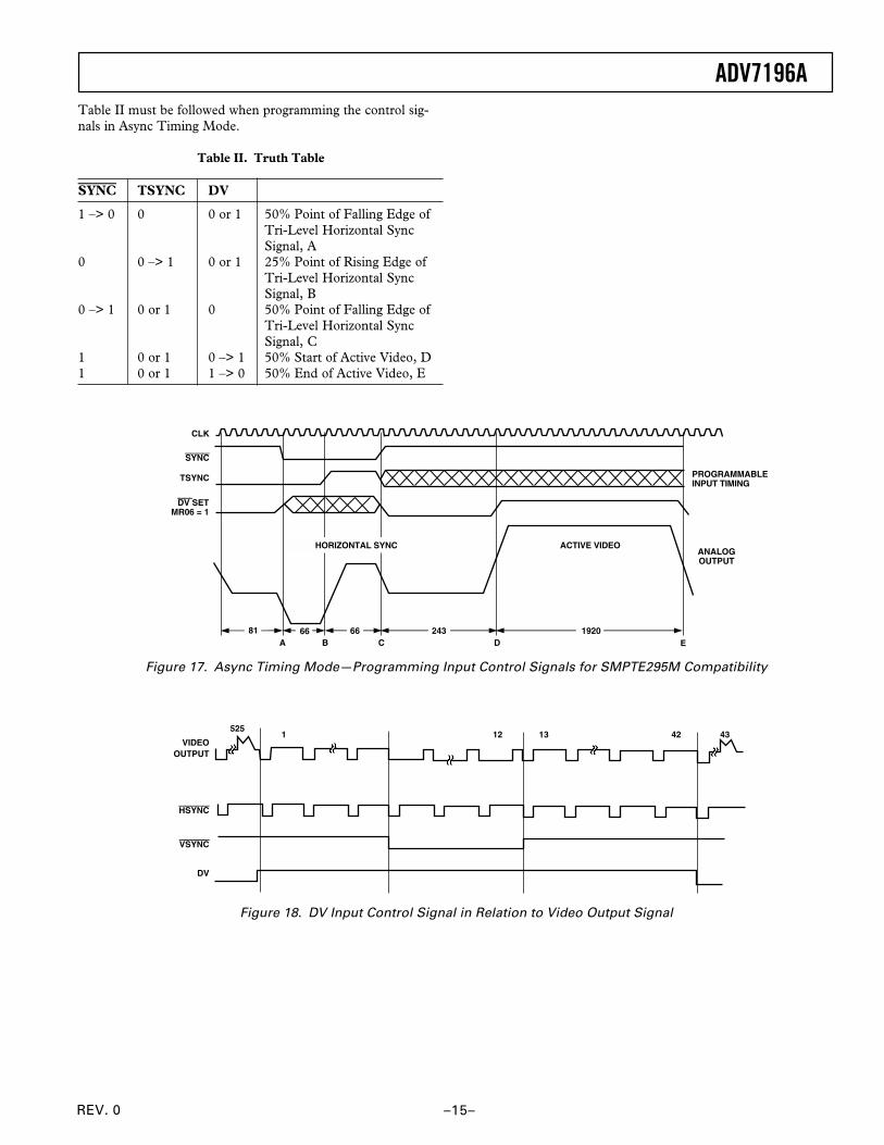
Table II must be followed when programming the control sig-nals in Async Timing Mode.
Table II. Truth Table
SYNC TSYNC DV
1 –> 0 0 0 or 1 50% Point of Falling Edge ofTri-Level Horizontal SyncSignal, A
0 0 –> 1 0 or 1 25% Point of Rising Edge ofTri-Level Horizontal SyncSignal, B
0 –> 1 0 or 1 0 50% Point of Falling Edge ofTri-Level Horizontal SyncSignal, C
1 0 or 1 0 –> 1 50% Start of Active Video, D1 0 or 1 1 –> 0 50% End of Active Video, E
A B C D E
CLK
SYNC
TSYNC
DV SET MR06 = 1
PROGRAMMABLEINPUT TIMING
ANALOGOUTPUT
ACTIVE VIDEOHORIZONTAL SYNC
6681 66 243 1920
Figure 17. Async Timing Mode—Programming Input Control Signals for SMPTE295M Compatibility
VIDEOOUTPUT
HSYNC
525
VSYNC
DV
1 12 13 42 43
Figure 18. DV Input Control Signal in Relation to Video Output Signal
REV. 0
ADV7196A
–16–
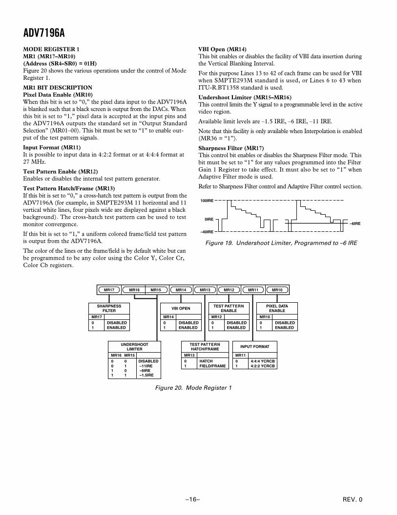
VBI Open (MR14)This bit enables or disables the facility of VBI data insertion duringthe Vertical Blanking Interval.
For this purpose Lines 13 to 42 of each frame can be used for VBIwhen SMPTE293M standard is used, or Lines 6 to 43 whenITU-R.BT1358 standard is used.
Undershoot Limiter (MR15–MR16)This control limits the Y signal to a programmable level in the activevideo region.
Available limit levels are –1.5 IRE, –6 IRE, –11 IRE.
Note that this facility is only available when Interpolation is enabled(MR36 = “1”).
Sharpness Filter (MR17)This control bit enables or disables the Sharpness Filter mode. Thisbit must be set to “1” for any values programmed into the FilterGain 1 Register to take effect. It must also be set to “1” whenAdaptive Filter mode is used.
Refer to Sharpness Filter control and Adaptive Filter control section.
–6IRE
100IRE
0IRE
–40IRE
Figure 19. Undershoot Limiter, Programmed to –6 IRE
MODE REGISTER 1MR1 (MR17–MR10)(Address (SR4–SR0) = 01H)Figure 20 shows the various operations under the control of ModeRegister 1.
MR1 BIT DESCRIPTIONPixel Data Enable (MR10)When this bit is set to “0,” the pixel data input to the ADV7196Ais blanked such that a black screen is output from the DACs. Whenthis bit is set to “1,” pixel data is accepted at the input pins andthe ADV7196A outputs the standard set in “Output StandardSelection” (MR01–00). This bit must be set to “1” to enable out-put of the test pattern signals.
Input Format (MR11)It is possible to input data in 4:2:2 format or at 4:4:4 format at27 MHz.
Test Pattern Enable (MR12)Enables or disables the internal test pattern generator.
Test Pattern Hatch/Frame (MR13)If this bit is set to “0,” a cross-hatch test pattern is output from theADV7196A (for example, in SMPTE293M 11 horizontal and 11vertical white lines, four pixels wide are displayed against a blackbackground). The cross-hatch test pattern can be used to testmonitor convergence.
If this bit is set to “1,” a uniform colored frame/field test patternis output from the ADV7196A.
The color of the lines or the frame/field is by default white but canbe programmed to be any color using the Color Y, Color Cr,Color Cb registers.
MR11MR17 MR12MR14MR15MR16
MR17
0 DISABLED1 ENABLED
SHARPNESSFILTER
MR13 MR10
MR14
0 DISABLED1 ENABLED
VBI OPEN
MR12
0 DISABLED1 ENABLED
TEST PATTERNENABLE
MR10
0 DISABLED1 ENABLED
PIXEL DATAENABLE
MR16 MR15
0 0 DISABLED0 1 –11IRE1 0 –6IRE1 1 –1.5IRE
UNDERSHOOTLIMITER
MR13
0 HATCH1 FIELD/FRAME
TEST PATTERNHATCH/FRAME
MR11
0 4:4:4 YCRCB1 4:2:2 YCRCB
INPUT FORMAT
Figure 20. Mode Register 1
REV. 0
ADV7196A
–17–
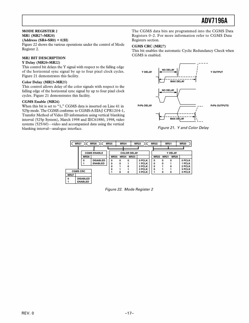
MODE REGISTER 2MR1 (MR27–MR20)(Address (SR4–SR0) = 02H)Figure 22 shows the various operations under the control of ModeRegister 2.
MR2 BIT DESCRIPTIONY Delay (MR20–MR22)This control bit delays the Y signal with respect to the falling edgeof the horizontal sync signal by up to four pixel clock cycles.Figure 21 demonstrates this facility.
Color Delay (MR23–MR25)This control allows delay of the color signals with respect to thefalling edge of the horizontal sync signal by up to four pixel clockcycles. Figure 21 demonstrates this facility.
CGMS Enable (MR26)When this bit is set to “1,” CGMS data is inserted on Line 41 in525p mode. The CGMS conforms: to CGMS-A EIA-J CPR1204-1,Transfer Method of Video ID information using vertical blankinginterval (525p System), March 1998 and IEC61880, 1998, videosystems (525/60)—video and accompanied data using the verticalblanking interval—analogue interface.
The CGMS data bits are programmed into the CGMS DataRegisters 0–2. For more information refer to CGMS DataRegisters section.
CGMS CRC (MR27)This bit enables the automatic Cyclic Redundancy Check whenCGMS is enabled.
MAX DELAY
NO DELAY
NO DELAY
MAX DELAY
PrPb DELAY
Y DELAY Y OUTPUT
PrPb OUTPUTS
Figure 21. Y and Color Delay
MR21MR27 MR22MR24MR25 MR23 MR20MR26
MR27
0 DISABLED1 ENABLED
CGMS CRC
MR26
0 DISABLED1 ENABLED
CGMS ENABLE
MR25 MR24 MR23
0 0 0 0 PCLK0 0 1 1 PCLK0 1 0 2 PCLK0 1 1 3 PCLK1 0 0 4 PCLK
COLOR DELAY
MR22 MR21 MR20
0 0 0 0 PCLK0 0 1 1 PCLK0 1 0 2 PCLK0 1 1 3 PCLK1 0 0 4 PCLK
Y DELAY
Figure 22. Mode Register 2
REV. 0
ADV7196A
–18–
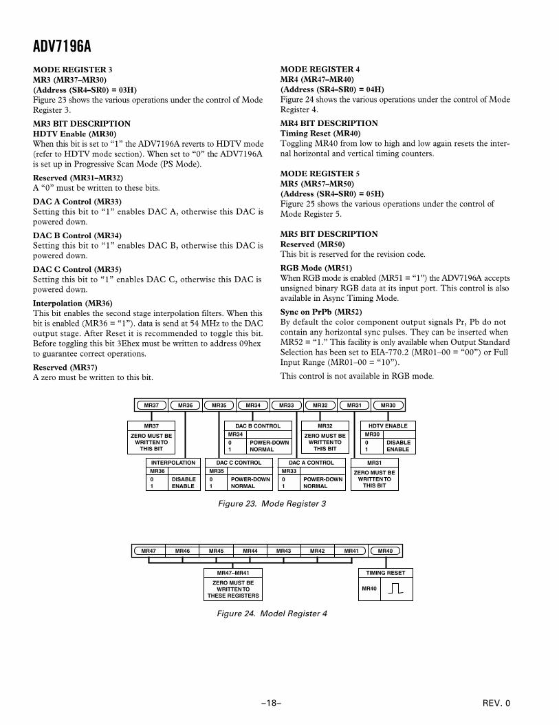
MODE REGISTER 4MR4 (MR47–MR40)(Address (SR4–SR0) = 04H)Figure 24 shows the various operations under the control of ModeRegister 4.
MR4 BIT DESCRIPTIONTiming Reset (MR40)Toggling MR40 from low to high and low again resets the inter-nal horizontal and vertical timing counters.
MODE REGISTER 5MR5 (MR57–MR50)(Address (SR4–SR0) = 05H)Figure 25 shows the various operations under the control ofMode Register 5.
MR5 BIT DESCRIPTIONReserved (MR50)This bit is reserved for the revision code.
RGB Mode (MR51)When RGB mode is enabled (MR51 = “1”) the ADV7196A acceptsunsigned binary RGB data at its input port. This control is alsoavailable in Async Timing Mode.
Sync on PrPb (MR52)By default the color component output signals Pr, Pb do notcontain any horizontal sync pulses. They can be inserted whenMR52 = “1.” This facility is only available when Output StandardSelection has been set to EIA-770.2 (MR01–00 = “00”) or FullInput Range (MR01–00 = “10”).
This control is not available in RGB mode.
MODE REGISTER 3MR3 (MR37–MR30)(Address (SR4–SR0) = 03H)Figure 23 shows the various operations under the control of ModeRegister 3.
MR3 BIT DESCRIPTIONHDTV Enable (MR30)When this bit is set to “1” the ADV7196A reverts to HDTV mode(refer to HDTV mode section). When set to “0” the ADV7196Ais set up in Progressive Scan Mode (PS Mode).
Reserved (MR31–MR32)A “0” must be written to these bits.
DAC A Control (MR33)Setting this bit to “1” enables DAC A, otherwise this DAC ispowered down.
DAC B Control (MR34)Setting this bit to “1” enables DAC B, otherwise this DAC ispowered down.
DAC C Control (MR35)Setting this bit to “1” enables DAC C, otherwise this DAC ispowered down.
Interpolation (MR36)This bit enables the second stage interpolation filters. When thisbit is enabled (MR36 = “1”). data is send at 54 MHz to the DACoutput stage. After Reset it is recommended to toggle this bit.Before toggling this bit 3Ehex must be written to address 09hexto guarantee correct operations.
Reserved (MR37)A zero must be written to this bit.
MR37 MR32MR34MR36
ZERO MUST BEWRITTEN TO
THIS BIT
MR37
MR34
0 POWER-DOWN1 NORMAL
DAC B CONTROL
MR35
MR36
0 DISABLE1 ENABLE
INTERPOLATION
MR35
0 POWER-DOWN1 NORMAL
DAC C CONTROL
MR33
ZERO MUST BEWRITTEN TO
THIS BIT
MR32
MR31
MR30
0 DISABLE1 ENABLE
HDTV ENABLE
MR30
MR33
0 POWER-DOWN1 NORMAL
DAC A CONTROL
ZERO MUST BEWRITTEN TO
THIS BIT
MR31
Figure 23. Mode Register 3
MR47 MR42MR44MR46
ZERO MUST BEWRITTEN TO
THESE REGISTERS
MR47–MR41
MR45 MR43 MR41 MR40
MR40
TIMING RESET
Figure 24. Model Register 4
REV. 0
ADV7196A
–19–
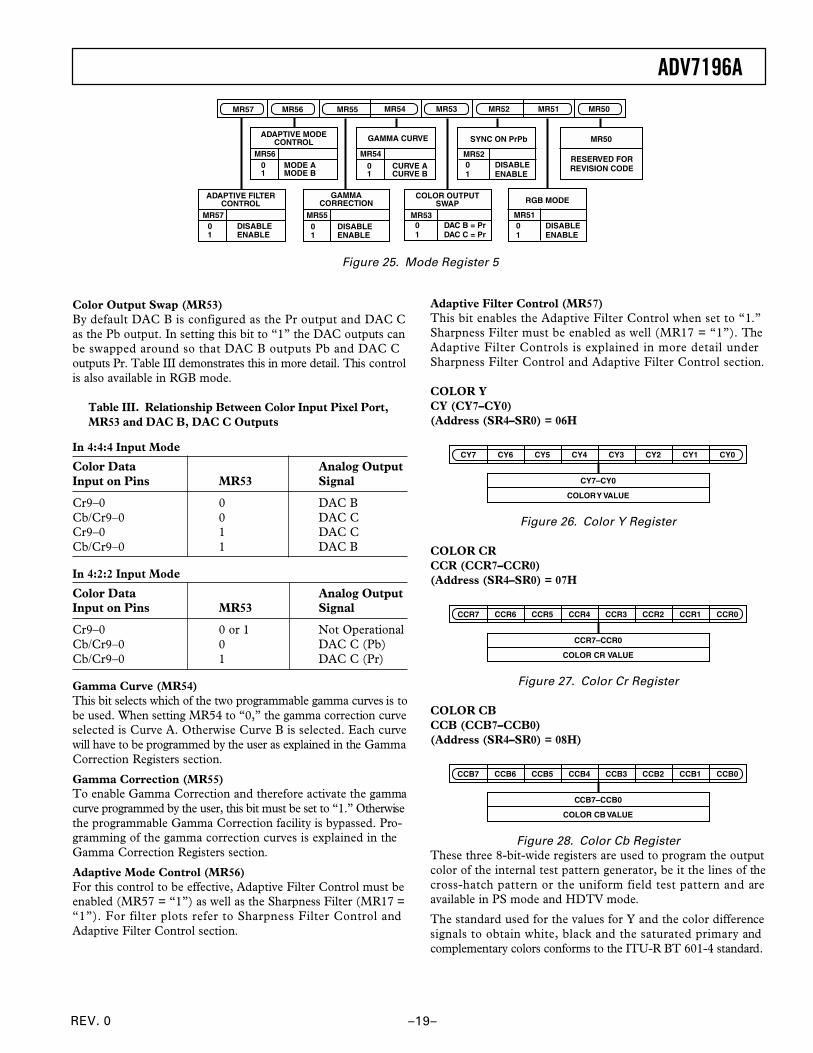
Color Output Swap (MR53)By default DAC B is configured as the Pr output and DAC Cas the Pb output. In setting this bit to “1” the DAC outputs canbe swapped around so that DAC B outputs Pb and DAC Coutputs Pr. Table III demonstrates this in more detail. This controlis also available in RGB mode.
Table III. Relationship Between Color Input Pixel Port,MR53 and DAC B, DAC C Outputs
In 4:4:4 Input Mode
Color Data Analog OutputInput on Pins MR53 Signal
Cr9–0 0 DAC BCb/Cr9–0 0 DAC CCr9–0 1 DAC CCb/Cr9–0 1 DAC B
In 4:2:2 Input Mode
Color Data Analog OutputInput on Pins MR53 Signal
Cr9–0 0 or 1 Not OperationalCb/Cr9–0 0 DAC C (Pb)Cb/Cr9–0 1 DAC C (Pr)
Gamma Curve (MR54)This bit selects which of the two programmable gamma curves is tobe used. When setting MR54 to “0,” the gamma correction curveselected is Curve A. Otherwise Curve B is selected. Each curvewill have to be programmed by the user as explained in the GammaCorrection Registers section.
Gamma Correction (MR55)To enable Gamma Correction and therefore activate the gammacurve programmed by the user, this bit must be set to “1.” Otherwisethe programmable Gamma Correction facility is bypassed. Pro-gramming of the gamma correction curves is explained in theGamma Correction Registers section.
Adaptive Mode Control (MR56)For this control to be effective, Adaptive Filter Control must beenabled (MR57 = “1”) as well as the Sharpness Filter (MR17 =“1”). For filter plots refer to Sharpness Filter Control andAdaptive Filter Control section.
Adaptive Filter Control (MR57)This bit enables the Adaptive Filter Control when set to “1.”Sharpness Filter must be enabled as well (MR17 = “1”). TheAdaptive Filter Controls is explained in more detail underSharpness Filter Control and Adaptive Filter Control section.
COLOR YCY (CY7–CY0)(Address (SR4–SR0) = 06H
CY7 CY6 CY5 CY4 CY3 CY2 CY1 CY0
CY7–CY0
COLOR Y VALUE
Figure 26. Color Y Register
COLOR CRCCR (CCR7–CCR0)(Address (SR4–SR0) = 07H
CCR7 CCR6 CCR5 CCR4 CCR3 CCR2 CCR1 CCR0
CCR7–CCR0
COLOR CR VALUE
Figure 27. Color Cr Register
COLOR CBCCB (CCB7–CCB0)(Address (SR4–SR0) = 08H)
CCB7 CCB6 CCB5 CCB4 CCB3 CCB2 CCB1 CCB0
CCB7–CCB0
COLOR CB VALUE
Figure 28. Color Cb RegisterThese three 8-bit-wide registers are used to program the outputcolor of the internal test pattern generator, be it the lines of thecross-hatch pattern or the uniform field test pattern and areavailable in PS mode and HDTV mode.
The standard used for the values for Y and the color differencesignals to obtain white, black and the saturated primary andcomplementary colors conforms to the ITU-R BT 601-4 standard.
COLOR OUTPUTSWAP
RESERVED FORREVISION CODE
MR50
MR57 MR56 MR55 MR54 MR53 MR52 MR51 MR50
0 MODE A1 MODE B
MR56
ADAPTIVE MODECONTROL
MR57
ADAPTIVE FILTERCONTROL
0 DISABLE 1 ENABLE
MR55
GAMMACORRECTION
0 DISABLE1 ENABLE
SYNC ON PrPb
MR52 0 DISABLE 1 ENABLE
0 CURVE A1 CURVE B
MR54
GAMMA CURVE
RGB MODE
MR51 0 DISABLE 1 ENABLE
MR53 0 DAC B = Pr 1 DAC C = Pr
Figure 25. Mode Register 5
REV. 0
ADV7196A
–20–
The Table IV shows sample color values to be programmed intothe color registers when Output Standard Selection is set toEIA-770.2 (MR01–00 = “00”).
Table IV. Sample Color Values for EIA 770.2 OutputStandard Selection
Sample Color Y Color Cr Color CbColor Value Value Value
White 235 (EB) 128 (80) 128 (80)Black 16 (10) 128 (80) 128 (80)Red 81 (51) 240 (F0) 90 (5A)Green 145 (91) 34 (22) 54 (36)Blue 41 (29) 110 (6E) 240 (F0)Yellow 210 (D2) 146 (92) 16 (10)Cyan 170 (AA) 16 (10) 166 (A6)Magenta 106 (6A) 222 (DE) 202 (CA)
MODE REGISTER 6MR6 (MR67–MR60)(Address (SR4–SR0) = 09H)Figure 29 shows the various operations under the control ofMode Register 6.
MR6 BIT DESCRIPTIONMR67–MR60The value 3Ehex must be written to this register before thePLL is reset (reset MR36) to guarantee correct operation ofthe ADV7196A.
MR67
ZERO MUST BEWRITTEN TO
THIS BIT
MR60
MR66 MR65 MR64 MR63 MR62 MR61 MR60
ONE MUST BEWRITTEN TO
THIS BIT
MR62
ONE MUST BEWRITTEN TO
THIS BIT
MR64
ZERO MUST BEWRITTEN TO
THIS BIT
MR66
ONE MUST BEWRITTEN TO
THIS BIT
MR61
ONE MUST BEWRITTEN TO
THIS BIT
MR63
ONE MUST BEWRITTEN TO
THIS BIT
MR65
ZERO MUST BEWRITTEN TO
THIS BIT
MR67
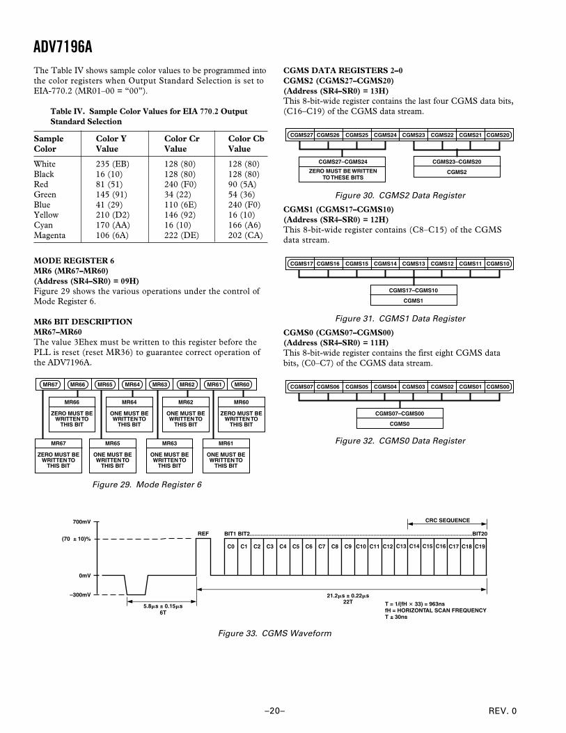
Figure 29. Mode Register 6
CGMS DATA REGISTERS 2–0CGMS2 (CGMS27–CGMS20)(Address (SR4–SR0) = 13H)This 8-bit-wide register contains the last four CGMS data bits,(C16–C19) of the CGMS data stream.
CGMS23–CGMS20
CGMS2
CGMS27 CGMS26 CGMS25 CGMS24 CGMS23 CGMS22 CGMS21 CGMS20
CGMS27–CGMS24
ZERO MUST BE WRITTENTO THESE BITS
Figure 30. CGMS2 Data Register
CGMS1 (CGMS17–CGMS10)(Address (SR4–SR0) = 12H)This 8-bit-wide register contains (C8–C15) of the CGMSdata stream.
CGMS17–CGMS10
CGMS1
CGMS17 CGMS16 CGMS15 CGMS14 CGMS13 CGMS12 CGMS11 CGMS10
Figure 31. CGMS1 Data Register
CGMS0 (CGMS07–CGMS00)(Address (SR4–SR0) = 11H)This 8-bit-wide register contains the first eight CGMS databits, (C0–C7) of the CGMS data stream.
CGMS07–CGMS00
CGMS0
CGMS07 CGMS06 CGMS05 CGMS04 CGMS03 CGMS02 CGMS01 CGMS00
Figure 32. CGMS0 Data Register
CRC SEQUENCE
21.2s 0.22s22T
REF
C0 C1 C2 C3 C4 C5 C6 C7 C8 C9 C10 C11 C12 C13 C14 C15 C16 C17 C18 C19
700mV
(70 10)%
0mV
–300mV
BIT1 BIT2................................................................................................................................................BIT20
5.8s 0.15s6T
T = 1/(fH 33) = 963nsfH = HORIZONTAL SCAN FREQUENCYT 30ns
Figure 33. CGMS Waveform
REV. 0
ADV7196A
–21–
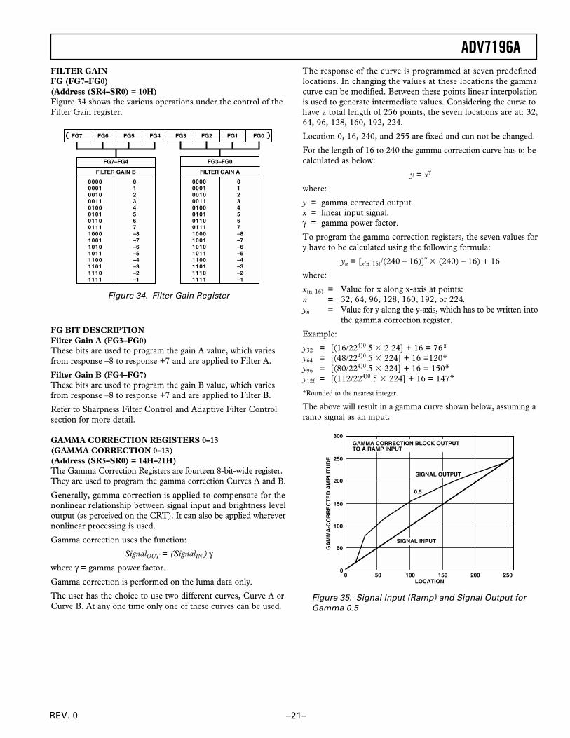
The response of the curve is programmed at seven predefinedlocations. In changing the values at these locations the gammacurve can be modified. Between these points linear interpolationis used to generate intermediate values. Considering the curve tohave a total length of 256 points, the seven locations are at: 32,64, 96, 128, 160, 192, 224.
Location 0, 16, 240, and 255 are fixed and can not be changed.
For the length of 16 to 240 the gamma correction curve has to becalculated as below:
y = xγ
where:
y = gamma corrected output.x = linear input signal.γ = gamma power factor.
To program the gamma correction registers, the seven values fory have to be calculated using the following formula:
yn = [x(n–16)/(240 – 16)]γ (240) – 16) + 16
where:
x(n–16) = Value for x along x-axis at points:n = 32, 64, 96, 128, 160, 192, or 224.yn = Value for y along the y-axis, which has to be written into
the gamma correction register.
Example:
y32 = [(16/224)0.5 2 24] + 16 = 76*y64 = [(48/224)0.5 224] + 16 =120*y96 = [(80/224)0.5 224] + 16 = 150*y128 = [(112/224)0.5 224] + 16 = 147*
*Rounded to the nearest integer.
The above will result in a gamma curve shown below, assuming aramp signal as an input.
250
200
150
100
50
0
300
SIGNAL OUTPUT
SIGNAL INPUT
0.5
GAMMA CORRECTION BLOCK OUTPUTTO A RAMP INPUT
GA
MM
A-C
OR
RE
CT
ED
AM
PL
ITU
DE
0 50 100 150 200 250LOCATION
Figure 35. Signal Input (Ramp) and Signal Output forGamma 0.5
FILTER GAINFG (FG7–FG0)(Address (SR4–SR0) = 10H)Figure 34 shows the various operations under the control of theFilter Gain register.
FG7 FG6 FG5 FG4 FG3 FG2 FG1 FG0
FG7–FG4
FILTER GAIN B
0000 00001 10010 20011 30100 40101 50110 60111 71000 –81001 –71010 –61011 –51100 –41101 –31110 –21111 –1
FG3–FG0
FILTER GAIN A
0000 00001 10010 20011 30100 40101 50110 60111 71000 –81001 –71010 –61011 –51100 –41101 –31110 –21111 –1
Figure 34. Filter Gain Register
FG BIT DESCRIPTIONFilter Gain A (FG3–FG0)These bits are used to program the gain A value, which variesfrom response –8 to response +7 and are applied to Filter A.
Filter Gain B (FG4–FG7)These bits are used to program the gain B value, which variesfrom response –8 to response +7 and are applied to Filter B.
Refer to Sharpness Filter Control and Adaptive Filter Controlsection for more detail.
GAMMA CORRECTION REGISTERS 0–13(GAMMA CORRECTION 0–13)(Address (SR5–SR0) = 14H–21H)The Gamma Correction Registers are fourteen 8-bit-wide register.They are used to program the gamma correction Curves A and B.
Generally, gamma correction is applied to compensate for thenonlinear relationship between signal input and brightness leveloutput (as perceived on the CRT). It can also be applied wherevernonlinear processing is used.
Gamma correction uses the function:
SignalOUT = (SignalIN ) γwhere γ = gamma power factor.
Gamma correction is performed on the luma data only.
The user has the choice to use two different curves, Curve A orCurve B. At any one time only one of these curves can be used.
REV. 0
ADV7196A
–22–
250
200
150
100
50
0
300
SIGNAL OUTPUTS
SIGNAL INPUT
0.5
GAMMA CORRECTION BLOCK OUTPUTTO A RAMP INPUT FOR VARIOUS GAMMA VALUES
GA
MM
A-C
OR
RE
CT
ED
AM
PL
ITU
DE
0 50 100 150 200 250LOCATION
0.3
1.5
1.8
Figure 36. Signal Input (Ramp) and Selectable GammaOutput Curves
The gamma curves shown above are examples only, any userdefined curve is acceptable in the range of 16–240.
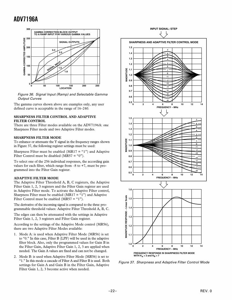
SHARPNESS FILTER CONTROL AND ADAPTIVEFILTER CONTROLThere are three Filter modes available on the ADV7196A: oneSharpness Filter mode and two Adaptive Filter modes.
SHARPNESS FILTER MODETo enhance or attenuate the Y signal in the frequency ranges shownin Figure 37, the following register settings must be used:
Sharpness Filter must be enabled (MR17 = “1”) and AdaptiveFilter Control must be disabled (MR57 = “0”).
To select one of the 256 individual responses, the according gainvalues for each filter, which range from –8 to +7, must be pro-grammed into the Filter Gain register.
ADAPTIVE FILTER MODEThe Adaptive Filter Threshold A, B, C registers, the AdaptiveFilter Gain 1, 2, 3 registers and the Filter Gain register are usedin Adaptive Filter mode. To activate the Adaptive Filter control,Sharpness Filter must be enabled (MR17 = “1”) and AdaptiveFilter Control must be enabled (MR57 = “1”).
The derivative of the incoming signal is compared to the three pro-grammable threshold values: Adaptive Filter Threshold A, B, C.
The edges can then be attenuated with the settings in AdaptiveFilter Gain 1, 2, 3 registers and Filter Gain register.
According to the settings of the Adaptive Mode control (MR56),there are two Adaptive Filter Modes available:
1. Mode A: is used when Adaptive Filter Mode (MR56) is setto “0.” In this case, Filter B (LPF) will be used in the adaptivefilter block. Also, only the programmed values for Gain B inthe Filter Gain, Adaptive Filter Gain 1, 2, 3 are applied whenneeded. The Gain A values are fixed and can not be changed.
2. Mode B: is used when Adaptive Filter Mode (MR56) is set to“1.” In this mode a cascade of Filter A and Filter B is used. Bothsettings for Gain A and Gain B in the Filter Gain, AdaptiveFilter Gain 1, 2, 3 become active when needed.
FREQUENCY – MHz
MA
GN
ITU
DE
1.5
1.4
1.3
1.2
1.1
1.0
0.9
0.8
0.7
0.6
0.50 2 4 6 8 10 12 14
–8
–7–6
–5
–4
–3
–2
–1
0
1
2
3
4
56
7
FREQUENCY – MHz
MA
GN
ITU
DE
1.5
1.4
1.3
1.2
1.1
1.0
0.9
0.8
0.7
0.6
0.50 2 4 6 8 10 12 14
–8
–7
–6
–5
–4
–3
–2
–1
0
1
2
3
4
5
6
7
SHARPNESS AND ADAPTIVE FILTER CONTROL MODE
INPUT SIGNAL: STEP
FREQUENCY – MHz
MA
GN
ITU
DE
RE
SP
ON
SE
– L
inea
r S
cale
1.6
1.5
1.4
1.3
1.2
1.1
1.00 2 4 6 8 10 12 14
FREQUENCY RESPONSE IN SHARPNESS FILTER MODEWITH KA = 3 and KB = 7
Figure 37. Sharpness and Adaptive Filter Control Mode
REV. 0
ADV7196A
–23–
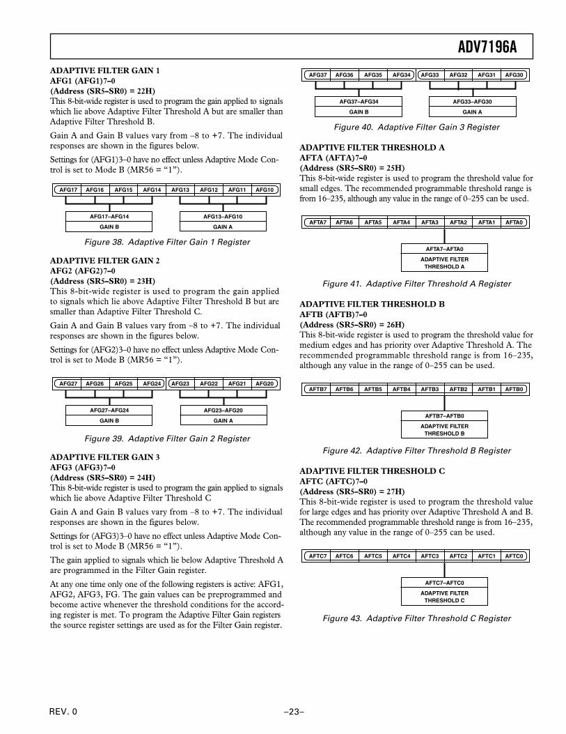
ADAPTIVE FILTER GAIN 1AFG1 (AFG1)7–0(Address (SR5–SR0) = 22H)This 8-bit-wide register is used to program the gain applied to signalswhich lie above Adaptive Filter Threshold A but are smaller thanAdaptive Filter Threshold B.
Gain A and Gain B values vary from –8 to +7. The individualresponses are shown in the figures below.
Settings for (AFG1)3–0 have no effect unless Adaptive Mode Con-trol is set to Mode B (MR56 = “1”).
AFG13–AFG10
GAIN A
AFG17 AFG16 AFG15 AFG14 AFG13 AFG12 AFG11 AFG10
AFG17–AFG14
GAIN B
Figure 38. Adaptive Filter Gain 1 Register
ADAPTIVE FILTER GAIN 2AFG2 (AFG2)7–0(Address (SR5–SR0) = 23H)This 8-bit-wide register is used to program the gain appliedto signals which lie above Adaptive Filter Threshold B but aresmaller than Adaptive Filter Threshold C.
Gain A and Gain B values vary from –8 to +7. The individualresponses are shown in the figures below.
Settings for (AFG2)3–0 have no effect unless Adaptive Mode Con-trol is set to Mode B (MR56 = “1”).
AFG23–AFG20
GAIN A
AFG27 AFG26 AFG25 AFG24 AFG23 AFG22 AFG21 AFG20
AFG27–AFG24
GAIN B
Figure 39. Adaptive Filter Gain 2 Register
ADAPTIVE FILTER GAIN 3AFG3 (AFG3)7–0(Address (SR5–SR0) = 24H)This 8-bit-wide register is used to program the gain applied to signalswhich lie above Adaptive Filter Threshold C
Gain A and Gain B values vary from –8 to +7. The individualresponses are shown in the figures below.
Settings for (AFG3)3–0 have no effect unless Adaptive Mode Con-trol is set to Mode B (MR56 = “1”).
The gain applied to signals which lie below Adaptive Threshold Aare programmed in the Filter Gain register.
At any one time only one of the following registers is active: AFG1,AFG2, AFG3, FG. The gain values can be preprogrammed andbecome active whenever the threshold conditions for the accord-ing register is met. To program the Adaptive Filter Gain registersthe source register settings are used as for the Filter Gain register.
AFG33–AFG30
GAIN A
AFG37 AFG36 AFG35 AFG34 AFG33 AFG32 AFG31 AFG30
AFG37–AFG34
GAIN B
Figure 40. Adaptive Filter Gain 3 Register
ADAPTIVE FILTER THRESHOLD AAFTA (AFTA)7–0(Address (SR5–SR0) = 25H)This 8-bit-wide register is used to program the threshold value forsmall edges. The recommended programmable threshold range isfrom 16–235, although any value in the range of 0–255 can be used.
AFTA7–AFTA0
ADAPTIVE FILTERTHRESHOLD A
AFTA7 AFTA6 AFTA5 AFTA4 AFTA3 AFTA2 AFTA1 AFTA0
Figure 41. Adaptive Filter Threshold A Register
ADAPTIVE FILTER THRESHOLD BAFTB (AFTB)7–0(Address (SR5–SR0) = 26H)This 8-bit-wide register is used to program the threshold value formedium edges and has priority over Adaptive Threshold A. Therecommended programmable threshold range is from 16–235,although any value in the range of 0–255 can be used.
AFTB7–AFTB0
ADAPTIVE FILTERTHRESHOLD B
AFTB7 AFTB6 AFTB5 AFTB4 AFTB3 AFTB2 AFTB1 AFTB0
Figure 42. Adaptive Filter Threshold B Register
ADAPTIVE FILTER THRESHOLD CAFTC (AFTC)7–0(Address (SR5–SR0) = 27H)This 8-bit-wide register is used to program the threshold valuefor large edges and has priority over Adaptive Threshold A and B.The recommended programmable threshold range is from 16–235,although any value in the range of 0–255 can be used.
AFTC7–AFTC0
ADAPTIVE FILTERTHRESHOLD C
AFTC7 AFTC6 AFTC5 AFTC4 AFTC3 AFTC2 AFTC1 AFTC0
Figure 43. Adaptive Filter Threshold C Register
REV. 0
ADV7196A
–24–
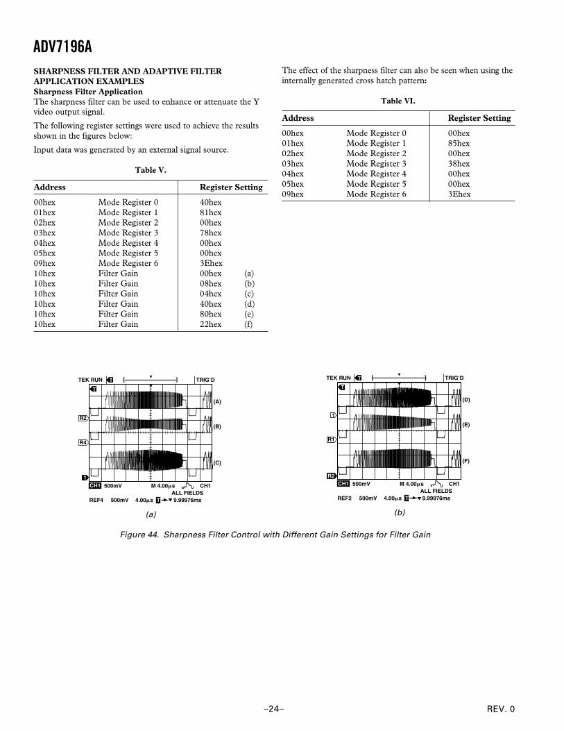
SHARPNESS FILTER AND ADAPTIVE FILTERAPPLICATION EXAMPLESSharpness Filter ApplicationThe sharpness filter can be used to enhance or attenuate the Yvideo output signal.
The following register settings were used to achieve the resultsshown in the figures below:
Input data was generated by an external signal source.
Table V.
Address Register Setting
00hex Mode Register 0 40hex01hex Mode Register 1 81hex02hex Mode Register 2 00hex03hex Mode Register 3 78hex04hex Mode Register 4 00hex05hex Mode Register 5 00hex09hex Mode Register 6 3Ehex10hex Filter Gain 00hex (a)10hex Filter Gain 08hex (b)10hex Filter Gain 04hex (c)10hex Filter Gain 40hex (d)10hex Filter Gain 80hex (e)10hex Filter Gain 22hex (f)
CH1
T
R2
R4
1
(B)
(C)
(A)
TEK RUN T TRIG’D
500mV M 4.00s
REF4 500mV 4.00s 9.99976msT
CH1ALL FIELDS
(a)
CH1
T
R2
R1
1
(E)
(F)
(D)
TEK RUN T TRIG’D
500mV M 4.00s
REF2 500mV 4.00s 9.99976msT
CH1ALL FIELDS
(b)
Figure 44. Sharpness Filter Control with Different Gain Settings for Filter Gain
The effect of the sharpness filter can also be seen when using theinternally generated cross hatch pattern:
Table VI.
Address Register Setting
00hex Mode Register 0 00hex01hex Mode Register 1 85hex02hex Mode Register 2 00hex03hex Mode Register 3 38hex04hex Mode Register 4 00hex05hex Mode Register 5 00hex09hex Mode Register 6 3Ehex
REV. 0
ADV7196A
–25–
In toggling MR17 (Sharpness Filter Enable/Disable) and settingthe Filter Gain register value to 99hex it can be seen that the linecontours of the cross hatch pattern change their sharpness.
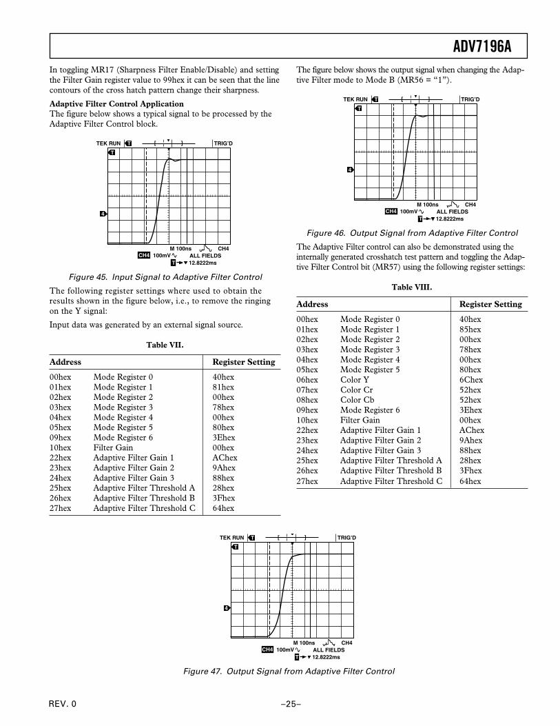
Adaptive Filter Control ApplicationThe figure below shows a typical signal to be processed by theAdaptive Filter Control block.
T
4
TEK RUN T TRIG’D
M 100ns
12.8222msT
CH4ALL FIELDSCH4 100mV
Figure 45. Input Signal to Adaptive Filter Control
The following register settings where used to obtain theresults shown in the figure below, i.e., to remove the ringingon the Y signal:
Input data was generated by an external signal source.
Table VII.
Address Register Setting
00hex Mode Register 0 40hex01hex Mode Register 1 81hex02hex Mode Register 2 00hex03hex Mode Register 3 78hex04hex Mode Register 4 00hex05hex Mode Register 5 80hex09hex Mode Register 6 3Ehex10hex Filter Gain 00hex22hex Adaptive Filter Gain 1 AChex23hex Adaptive Filter Gain 2 9Ahex24hex Adaptive Filter Gain 3 88hex25hex Adaptive Filter Threshold A 28hex26hex Adaptive Filter Threshold B 3Fhex27hex Adaptive Filter Threshold C 64hex
The figure below shows the output signal when changing the Adap-tive Filter mode to Mode B (MR56 = “1”).
T
4
TEK RUN T TRIG’D
M 100ns
12.8222msT
CH4ALL FIELDSCH4 100mV
Figure 46. Output Signal from Adaptive Filter Control
The Adaptive Filter control can also be demonstrated using theinternally generated crosshatch test pattern and toggling the Adap-tive Filter Control bit (MR57) using the following register settings:
Table VIII.
Address Register Setting
00hex Mode Register 0 40hex01hex Mode Register 1 85hex02hex Mode Register 2 00hex03hex Mode Register 3 78hex04hex Mode Register 4 00hex05hex Mode Register 5 80hex06hex Color Y 6Chex07hex Color Cr 52hex08hex Color Cb 52hex09hex Mode Register 6 3Ehex10hex Filter Gain 00hex22hex Adaptive Filter Gain 1 AChex23hex Adaptive Filter Gain 2 9Ahex24hex Adaptive Filter Gain 3 88hex25hex Adaptive Filter Threshold A 28hex26hex Adaptive Filter Threshold B 3Fhex27hex Adaptive Filter Threshold C 64hex
T
4
TEK RUN T TRIG’D
M 100ns
12.8222msT
CH4ALL FIELDSCH4 100mV
Figure 47. Output Signal from Adaptive Filter Control
REV. 0
ADV7196A
–26–
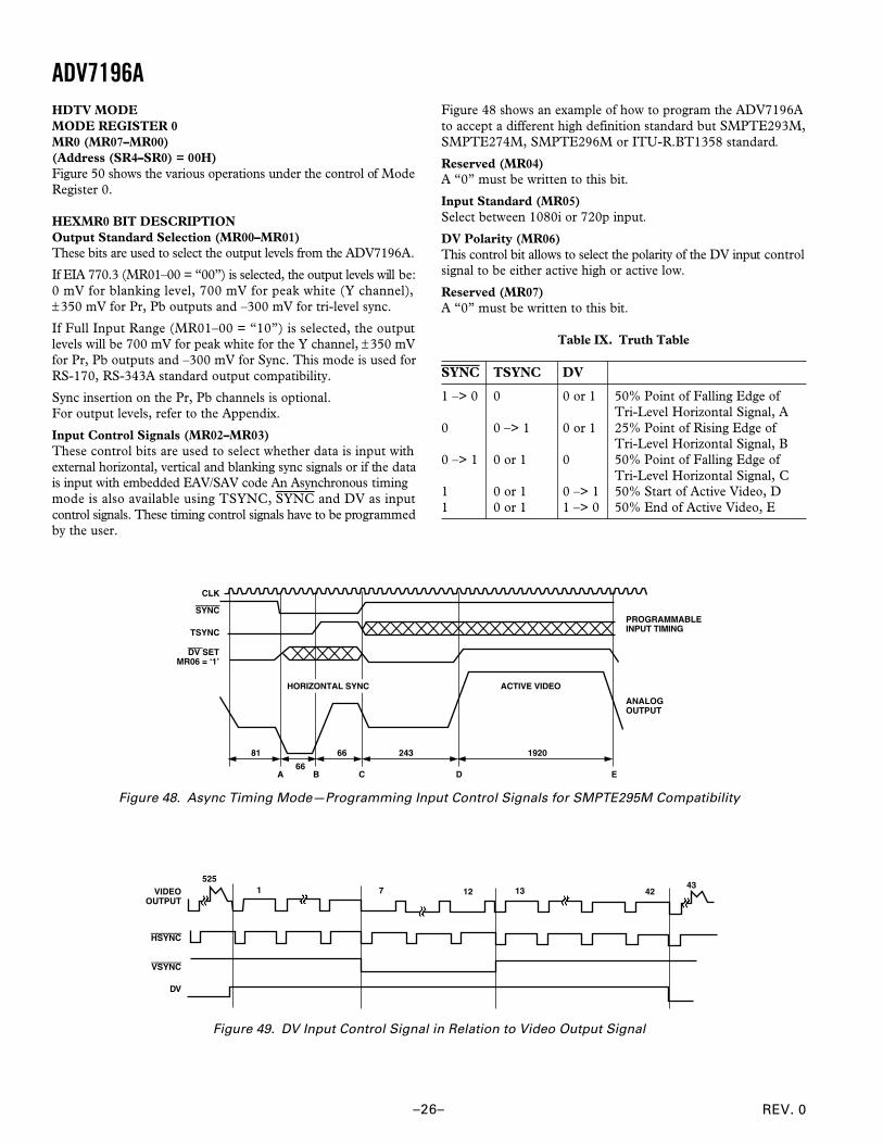
HDTV MODEMODE REGISTER 0MR0 (MR07–MR00)(Address (SR4–SR0) = 00H)Figure 50 shows the various operations under the control of ModeRegister 0.
HEXMR0 BIT DESCRIPTIONOutput Standard Selection (MR00–MR01)These bits are used to select the output levels from the ADV7196A.
If EIA 770.3 (MR01–00 = “00”) is selected, the output levels will be:0 mV for blanking level, 700 mV for peak white (Y channel),±350 mV for Pr, Pb outputs and –300 mV for tri-level sync.
If Full Input Range (MR01–00 = “10”) is selected, the outputlevels will be 700 mV for peak white for the Y channel, ±350 mVfor Pr, Pb outputs and –300 mV for Sync. This mode is used forRS-170, RS-343A standard output compatibility.
Sync insertion on the Pr, Pb channels is optional.For output levels, refer to the Appendix.
Input Control Signals (MR02–MR03)These control bits are used to select whether data is input withexternal horizontal, vertical and blanking sync signals or if the datais input with embedded EAV/SAV code An Asynchronous timingmode is also available using TSYNC, SYNC and DV as inputcontrol signals. These timing control signals have to be programmedby the user.
Figure 48 shows an example of how to program the ADV7196Ato accept a different high definition standard but SMPTE293M,SMPTE274M, SMPTE296M or ITU-R.BT1358 standard.
Reserved (MR04)A “0” must be written to this bit.
Input Standard (MR05)Select between 1080i or 720p input.
DV Polarity (MR06)This control bit allows to select the polarity of the DV input controlsignal to be either active high or active low.
Reserved (MR07)A “0” must be written to this bit.
Table IX. Truth Table
SYNC TSYNC DV
1 –> 0 0 0 or 1 50% Point of Falling Edge ofTri-Level Horizontal Signal, A
0 0 –> 1 0 or 1 25% Point of Rising Edge ofTri-Level Horizontal Signal, B
0 –> 1 0 or 1 0 50% Point of Falling Edge ofTri-Level Horizontal Signal, C
1 0 or 1 0 –> 1 50% Start of Active Video, D1 0 or 1 1 –> 0 50% End of Active Video, E
CLK
SYNC
TSYNC
DV SETMR06 = ‘1’
PROGRAMMABLEINPUT TIMING
ANALOGOUTPUT
A B C D E
243
ACTIVE VIDEO
192066
66
81
HORIZONTAL SYNC
Figure 48. Async Timing Mode—Programming Input Control Signals for SMPTE295M Compatibility
7VIDEOOUTPUT
HSYNC
525
VSYNC
DV
1 12 13 4243
Figure 49. DV Input Control Signal in Relation to Video Output Signal
REV. 0
ADV7196A
–27–
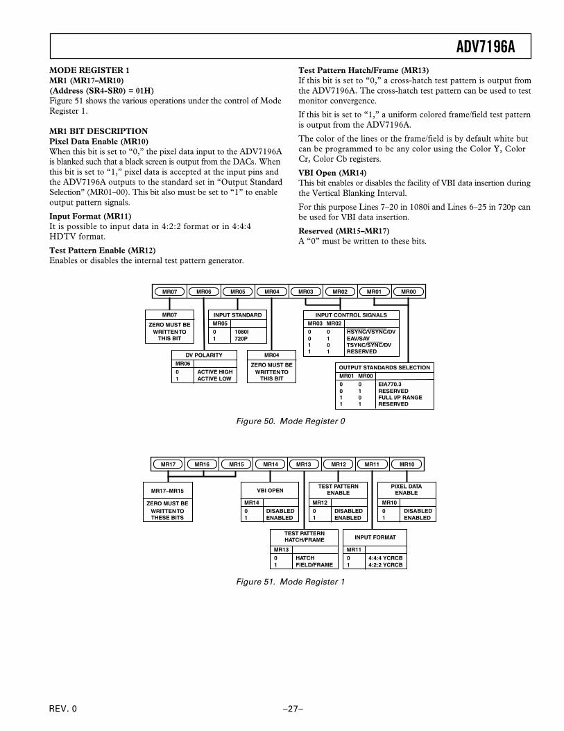
MODE REGISTER 1MR1 (MR17–MR10)(Address (SR4-SR0) = 01H)Figure 51 shows the various operations under the control of ModeRegister 1.
MR1 BIT DESCRIPTIONPixel Data Enable (MR10)When this bit is set to “0,” the pixel data input to the ADV7196Ais blanked such that a black screen is output from the DACs. Whenthis bit is set to “1,” pixel data is accepted at the input pins andthe ADV7196A outputs to the standard set in “Output StandardSelection” (MR01–00). This bit also must be set to “1” to enableoutput pattern signals.
Input Format (MR11)It is possible to input data in 4:2:2 format or in 4:4:4HDTV format.
Test Pattern Enable (MR12)Enables or disables the internal test pattern generator.
Test Pattern Hatch/Frame (MR13)If this bit is set to “0,” a cross-hatch test pattern is output fromthe ADV7196A. The cross-hatch test pattern can be used to testmonitor convergence.
If this bit is set to “1,” a uniform colored frame/field test patternis output from the ADV7196A.
The color of the lines or the frame/field is by default white butcan be programmed to be any color using the Color Y, ColorCr, Color Cb registers.
VBI Open (MR14)This bit enables or disables the facility of VBI data insertion duringthe Vertical Blanking Interval.
For this purpose Lines 7–20 in 1080i and Lines 6–25 in 720p canbe used for VBI data insertion.
Reserved (MR15–MR17)A “0” must be written to these bits.
MR01MR07 MR02MR04MR06
MR07
ZERO MUST BEWRITTEN TO
THIS BIT
MR03 MR00
MR03 MR02
0 0 HSYNC/VSYNC/DV0 1 EAV/SAV1 0 TSYNC/SYNC/DV1 1 RESERVED
INPUT CONTROL SIGNALS
MR05
MR06
0 ACTIVE HIGH1 ACTIVE LOW
DV POLARITY
MR05
0 1080I1 720P
INPUT STANDARD
MR04
ZERO MUST BEWRITTEN TO
THIS BIT MR01 MR00
0 0 EIA770.30 1 RESERVED1 0 FULL I/P RANGE1 1 RESERVED
OUTPUT STANDARDS SELECTION
Figure 50. Mode Register 0
MR11MR17 MR12MR14MR16 MR13 MR10
MR14
0 DISABLED1 ENABLED
VBI OPEN
MR12
0 DISABLED1 ENABLED
TEST PATTERNENABLE
MR10
0 DISABLED1 ENABLED
PIXEL DATAENABLE
MR13
0 HATCH1 FIELD/FRAME
TEST PATTERNHATCH/FRAME
MR11
0 4:4:4 YCRCB1 4:2:2 YCRCB
INPUT FORMAT
MR15
MR17–MR15
ZERO MUST BEWRITTEN TOTHESE BITS
Figure 51. Mode Register 1
REV. 0
ADV7196A
–28–
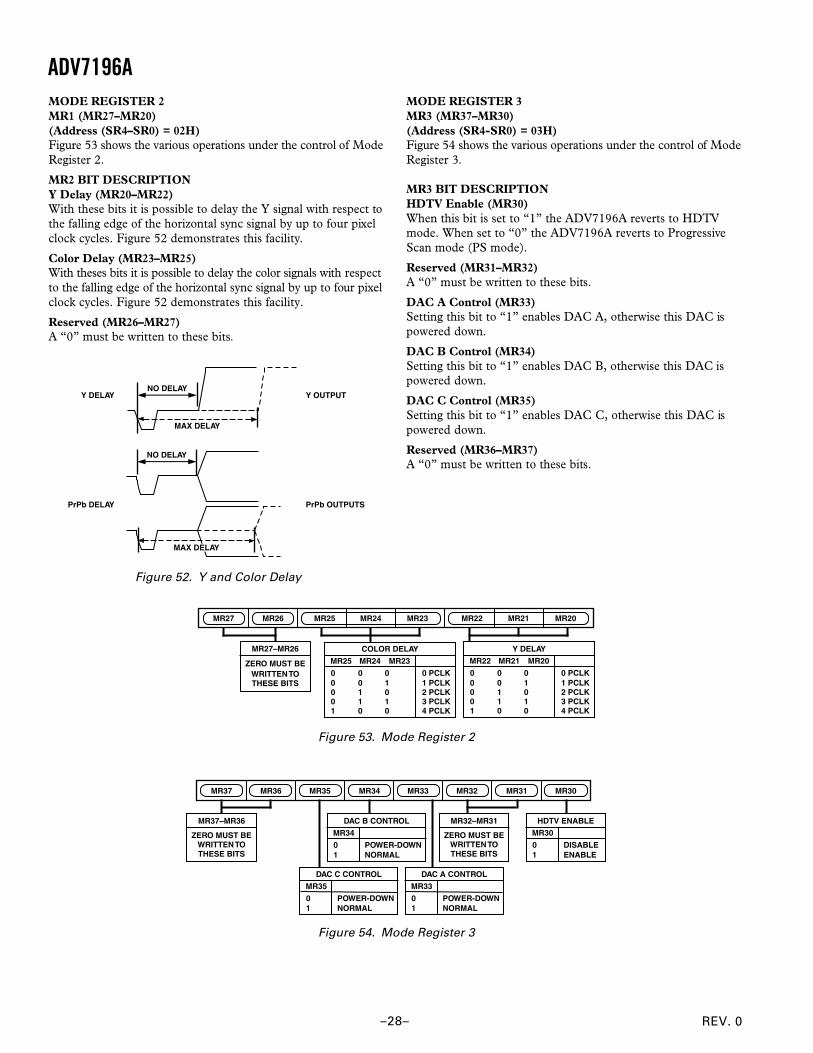
MODE REGISTER 2MR1 (MR27–MR20)(Address (SR4–SR0) = 02H)Figure 53 shows the various operations under the control of ModeRegister 2.
MR2 BIT DESCRIPTIONY Delay (MR20–MR22)With these bits it is possible to delay the Y signal with respect tothe falling edge of the horizontal sync signal by up to four pixelclock cycles. Figure 52 demonstrates this facility.
Color Delay (MR23–MR25)With theses bits it is possible to delay the color signals with respectto the falling edge of the horizontal sync signal by up to four pixelclock cycles. Figure 52 demonstrates this facility.
Reserved (MR26–MR27)A “0” must be written to these bits.
MAX DELAY
NO DELAY
NO DELAY
MAX DELAY
PrPb DELAY
Y DELAY Y OUTPUT
PrPb OUTPUTS
Figure 52. Y and Color Delay
MODE REGISTER 3MR3 (MR37–MR30)(Address (SR4-SR0) = 03H)Figure 54 shows the various operations under the control of ModeRegister 3.
MR3 BIT DESCRIPTIONHDTV Enable (MR30)When this bit is set to “1” the ADV7196A reverts to HDTVmode. When set to “0” the ADV7196A reverts to ProgressiveScan mode (PS mode).
Reserved (MR31–MR32)A “0” must be written to these bits.
DAC A Control (MR33)Setting this bit to “1” enables DAC A, otherwise this DAC ispowered down.
DAC B Control (MR34)Setting this bit to “1” enables DAC B, otherwise this DAC ispowered down.
DAC C Control (MR35)Setting this bit to “1” enables DAC C, otherwise this DAC ispowered down.
Reserved (MR36–MR37)A “0” must be written to these bits.
MR21MR27 MR22MR24MR25 MR23 MR20MR26
MR25 MR24 MR23
0 0 0 0 PCLK0 0 1 1 PCLK0 1 0 2 PCLK0 1 1 3 PCLK1 0 0 4 PCLK
COLOR DELAY
MR22 MR21 MR20
0 0 0 0 PCLK0 0 1 1 PCLK0 1 0 2 PCLK0 1 1 3 PCLK1 0 0 4 PCLK
Y DELAYMR27–MR26
ZERO MUST BEWRITTEN TOTHESE BITS
Figure 53. Mode Register 2
MR37 MR32MR34MR36
ZERO MUST BEWRITTEN TOTHESE BITS
MR37–MR36
MR34
0 POWER-DOWN1 NORMAL
DAC B CONTROL
MR35
MR35
0 POWER-DOWN1 NORMAL
DAC C CONTROL
MR33
ZERO MUST BEWRITTEN TOTHESE BITS
MR32–MR31
MR31
MR30
0 DISABLE1 ENABLE
HDTV ENABLE
MR30
MR33
0 POWER-DOWN1 NORMAL
DAC A CONTROL
Figure 54. Mode Register 3
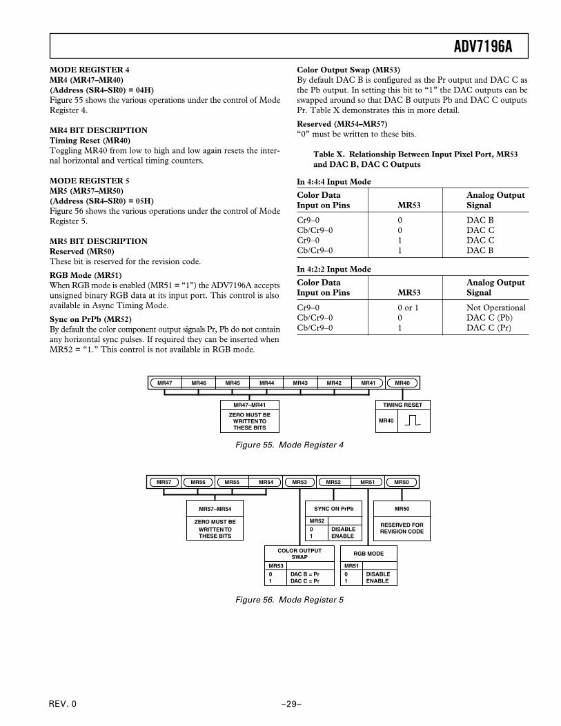
REV. 0
ADV7196A
–29–
MODE REGISTER 4MR4 (MR47–MR40)(Address (SR4–SR0) = 04H)Figure 55 shows the various operations under the control of ModeRegister 4.
MR4 BIT DESCRIPTIONTiming Reset (MR40)Toggling MR40 from low to high and low again resets the inter-nal horizontal and vertical timing counters.
MODE REGISTER 5MR5 (MR57–MR50)(Address (SR4–SR0) = 05H)Figure 56 shows the various operations under the control of ModeRegister 5.
MR5 BIT DESCRIPTIONReserved (MR50)These bit is reserved for the revision code.
RGB Mode (MR51)When RGB mode is enabled (MR51 = “1”) the ADV7196A acceptsunsigned binary RGB data at its input port. This control is alsoavailable in Async Timing Mode.
Sync on PrPb (MR52)By default the color component output signals Pr, Pb do not containany horizontal sync pulses. If required they can be inserted whenMR52 = “1.” This control is not available in RGB mode.
Color Output Swap (MR53)By default DAC B is configured as the Pr output and DAC C asthe Pb output. In setting this bit to “1” the DAC outputs can beswapped around so that DAC B outputs Pb and DAC C outputsPr. Table X demonstrates this in more detail.
Reserved (MR54–MR57)“0” must be written to these bits.
Table X. Relationship Between Input Pixel Port, MR53and DAC B, DAC C Outputs
In 4:4:4 Input Mode
Color Data Analog OutputInput on Pins MR53 Signal
Cr9–0 0 DAC BCb/Cr9–0 0 DAC CCr9–0 1 DAC CCb/Cr9–0 1 DAC B
In 4:2:2 Input Mode
Color Data Analog OutputInput on Pins MR53 Signal
Cr9–0 0 or 1 Not OperationalCb/Cr9–0 0 DAC C (Pb)Cb/Cr9–0 1 DAC C (Pr)
MR47 MR42MR44MR46
ZERO MUST BEWRITTEN TOTHESE BITS
MR47–MR41
MR45 MR43 MR41 MR40
MR40
TIMING RESET
Figure 55. Mode Register 4
MR57 MR52MR56
MR57–MR54
ZERO MUST BEWRITTEN TOTHESE BITS
MR55 MR53 MR51 MR50MR54
MR53
0 DAC B = Pr1 DAC C = Pr
COLOR OUTPUTSWAP
MR52
0 DISABLE1 ENABLE
SYNC ON PrPb
MR51
0 DISABLE1 ENABLE
RGB MODE
RESERVED FORREVISION CODE
MR50
Figure 56. Mode Register 5
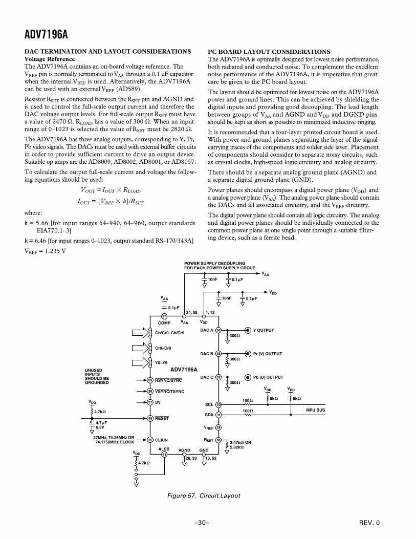
REV. 0
ADV7196A
–30–
DAC TERMINATION AND LAYOUT CONSIDERATIONSVoltage ReferenceThe ADV7196A contains an on-board voltage reference. TheVREF pin is normally terminated to VAA through a 0.1 µF capacitorwhen the internal VREF is used. Alternatively, the ADV7196Acan be used with an external VREF (AD589).
Resistor RSET is connected between the RSET pin and AGND andis used to control the full-scale output current and therefore theDAC voltage output levels. For full-scale output RSET must havea value of 2470 Ω. RLOAD has a value of 300 Ω. When an inputrange of 0–1023 is selected the value of RSET must be 2820 Ω.
The ADV7196A has three analog outputs, corresponding to Y, Pr,Pb video signals. The DACs must be used with external buffer circuitsin order to provide sufficient current to drive an output device.Suitable op amps are the AD8009, AD8002, AD8001, or AD8057.
To calculate the output full-scale current and voltage the follow-ing equations should be used:
VOUT = IOUT RLOAD
IOUT = [VREF k]/RSET
where:
k = 5.66 [for input ranges 64–940, 64–960, output standardsEIA770.1–3]
k = 6.46 [for input ranges 0–1023, output standard RS–170/343A]
VREF = 1.235 V
PC BOARD LAYOUT CONSIDERATIONSThe ADV7196A is optimally designed for lowest noise performance,both radiated and conducted noise. To complement the excellentnoise performance of the ADV7196A, it is imperative that greatcare be given to the PC board layout.
The layout should be optimized for lowest noise on the ADV7196Apower and ground lines. This can be achieved by shielding thedigital inputs and providing good decoupling. The lead lengthbetween groups of VAA and AGND and VDD and DGND pinsshould be kept as short as possible to minimized inductive ringing.
It is recommended that a four-layer printed circuit board is used.With power and ground planes separating the layer of the signalcarrying traces of the components and solder side layer. Placementof components should consider to separate noisy circuits, suchas crystal clocks, high-speed logic circuitry and analog circuitry.
There should be a separate analog ground plane (AGND) anda separate digital ground plane (GND).
Power planes should encompass a digital power plane (VDD) anda analog power plane (VAA). The analog power plane should containthe DACs and all associated circuitry, and the VREF circuitry.
The digital power plane should contain all logic circuitry. The analogand digital power planes should be individually connected to thecommon power plane at one single point through a suitable filter-ing device, such as a ferrite bead.
300
5k 5k
MPU BUS
4.7k
VDD
POWER SUPPLY DECOUPLINGFOR EACH POWER SUPPLY GROUP
ALSB
DV
RESET
CLKIN RSET
SDA
SCL
DAC A
VDD
VSYNC/TSYNC
ADV7196AUNUSEDINPUTSSHOULD BEGROUNDED
DAC B
100
HSYNC/SYNCDAC C
27MHz, 74.25MHz OR74.1758MHz CLOCK
4.7k
4.7F6.3V
300
300
100
2.47k OR2.82k
10nF 0.1F
Y OUTPUT
Pr (V) OUTPUT
Pb (U) OUTPUT
VREF
GND
13, 52
AGND
26, 33
Y0–Y9
Cr0–Cr9
Cb/Cr0–Cb/Cr9
0.1F
10nF 0.1F
24, 35 1, 12
VDD
VAA
COMP VAA
VAA
VDD
VDD VDD
Figure 57. Circuit Layout
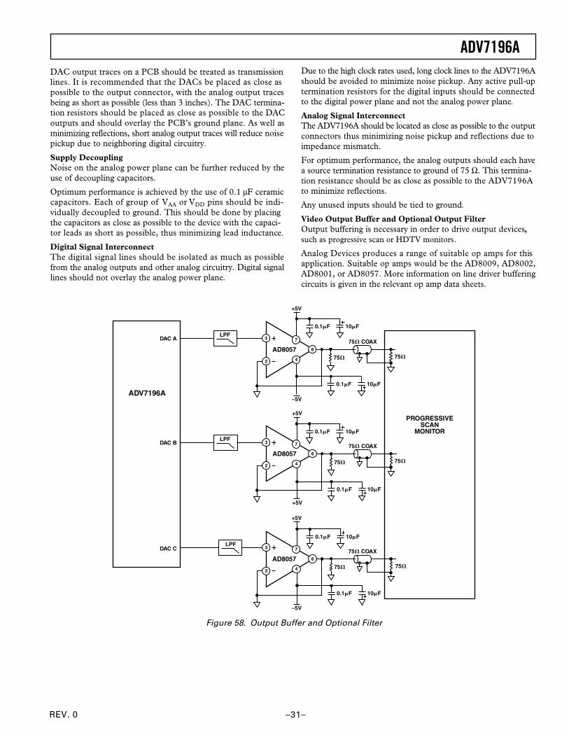
REV. 0
ADV7196A
–31–
ADV7196A
DAC A
DAC B
DAC C
AD8057
+5V
+5V
75 COAX
75
AD8057
–5V
0.1F 10F
+5V
75 COAX
75
AD8057
–5V
+5V
75 COAX
75
PROGRESSIVESCAN
MONITOR
75
LPF
LPF
LPF
0.1F 10F
0.1F 10F
0.1F 10F
0.1F 10F
0.1F 10F
75
75
Figure 58. Output Buffer and Optional Filter
DAC output traces on a PCB should be treated as transmissionlines. It is recommended that the DACs be placed as close aspossible to the output connector, with the analog output tracesbeing as short as possible (less than 3 inches). The DAC termina-tion resistors should be placed as close as possible to the DACoutputs and should overlay the PCB’s ground plane. As well asminimizing reflections, short analog output traces will reduce noisepickup due to neighboring digital circuitry.
Supply DecouplingNoise on the analog power plane can be further reduced by theuse of decoupling capacitors.
Optimum performance is achieved by the use of 0.1 µF ceramiccapacitors. Each of group of VAA or VDD pins should be indi-vidually decoupled to ground. This should be done by placingthe capacitors as close as possible to the device with the capaci-tor leads as short as possible, thus minimizing lead inductance.
Digital Signal InterconnectThe digital signal lines should be isolated as much as possiblefrom the analog outputs and other analog circuitry. Digital signallines should not overlay the analog power plane.
Due to the high clock rates used, long clock lines to the ADV7196Ashould be avoided to minimize noise pickup. Any active pull-uptermination resistors for the digital inputs should be connectedto the digital power plane and not the analog power plane.
Analog Signal InterconnectThe ADV7196A should be located as close as possible to the outputconnectors thus minimizing noise pickup and reflections due toimpedance mismatch.
For optimum performance, the analog outputs should each havea source termination resistance to ground of 75 Ω. This termina-tion resistance should be as close as possible to the ADV7196Ato minimize reflections.
Any unused inputs should be tied to ground.
Video Output Buffer and Optional Output FilterOutput buffering is necessary in order to drive output devices,such as progressive scan or HDTV monitors.
Analog Devices produces a range of suitable op amps for thisapplication. Suitable op amps would be the AD8009, AD8002,AD8001, or AD8057. More information on line driver bufferingcircuits is given in the relevant op amp data sheets.
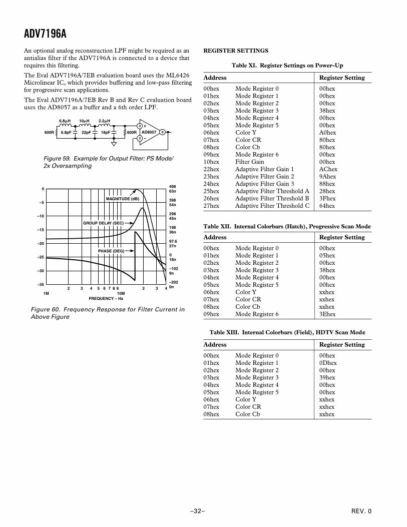
REV. 0
ADV7196A
–32–
REGISTER SETTINGS
Table XI. Register Settings on Power-Up
Address Register Setting
00hex Mode Register 0 00hex01hex Mode Register 1 00hex02hex Mode Register 2 00hex03hex Mode Register 3 38hex04hex Mode Register 4 00hex05hex Mode Register 5 00hex06hex Color Y A0hex07hex Color CR 80hex08hex Color Cb 80hex09hex Mode Register 6 00hex10hex Filter Gain 00hex22hex Adaptive Filter Gain 1 AChex23hex Adaptive Filter Gain 2 9Ahex24hex Adaptive Filter Gain 3 88hex25hex Adaptive Filter Threshold A 28hex26hex Adaptive Filter Threshold B 3Fhex27hex Adaptive Filter Threshold C 64hex
Table XII. Internal Colorbars (Hatch), Progressive Scan Mode
Address Register Setting
00hex Mode Register 0 00hex01hex Mode Register 1 05hex02hex Mode Register 2 00hex03hex Mode Register 3 38hex04hex Mode Register 4 00hex05hex Mode Register 5 00hex06hex Color Y xxhex07hex Color CR xxhex08hex Color Cb xxhex09hex Mode Register 6 3Ehex
Table XIII. Internal Colorbars (Field), HDTV Scan Mode
Address Register Setting
00hex Mode Register 0 00hex01hex Mode Register 1 0Dhex02hex Mode Register 2 00hex03hex Mode Register 3 39hex04hex Mode Register 4 00hex05hex Mode Register 5 00hex06hex Color Y xxhex07hex Color CR xxhex08hex Color Cb xxhex
An optional analog reconstruction LPF might be required as anantialias filter if the ADV7196A is connected to a device thatrequires this filtering.
The Eval ADV7196A/7EB evaluation board uses the ML6426Microlinear IC, which provides buffering and low-pass filteringfor progressive scan applications.
The Eval ADV7196A/7EB Rev B and Rev C evaluation boarduses the AD8057 as a buffer and a 6th order LPF.
AD8057600R18pF
2.2H
22pF
10H
6.8pF
6.8H
600R
Figure 59. Example for Output Filter: PS Mode/2x Oversampling
0
1M
–5
–10
–15
–20
–25
–30
–352 3 4 5 6 7 8 9
10MFREQUENCY – Hz
2 3 4
49863n
39854n
29845n
19836n
97.627n
018n
–1029n
–2020n
MAGNITUDE (dB)
PHASE (DEG)
GROUP DELAY (SEC)
Figure 60. Frequency Response for Filter Current inAbove Figure
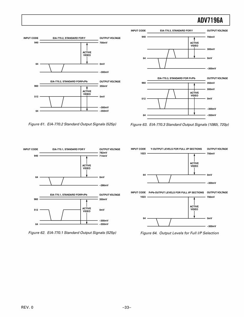
REV. 0
ADV7196A
–33–
940
64
ACTIVEVIDEO
700mV
0mV
–300mV
OUTPUT VOLTAGEINPUT CODE EIA-770.2, STANDARD FOR Y
960
64
ACTIVEVIDEO
350mV
–300mV–350mV
OUTPUT VOLTAGEEIA-770.2, STANDARD FORPr/Pb
0mV512
Figure 61. EIA-770.2 Standard Output Signals (525p)
940
64
714mV
0mV
–286mV
OUTPUT VOLTAGEINPUT CODE EIA-770.1, STANDARD FOR Y
ACTIVEVIDEO
782mV
960
64
ACTIVEVIDEO
350mV
–300mV–350mV
OUTPUT VOLTAGEEIA-770.1, STANDARD FORPr/Pb
0mV512
Figure 62. EIA-770.1 Standard Output Signals (525p)
940
64
ACTIVEVIDEO
700mV
300mV
–300mV
OUTPUT VOLTAGEINPUT CODE EIA-770.3, STANDARD FOR Y
0mV
960
64
ACTIVEVIDEO
350mV
300mV
–300mV
OUTPUT VOLTAGEEIA-770.3, STANDARD FOR Pr/Pb
0mV512
–350mV
Figure 63. EIA-770.3 Standard Output Signals (1080i, 720p)
1023
64
ACTIVEVIDEO
700mV
0mV
–300mV
OUTPUT VOLTAGEINPUT CODE Y-OUTPUT LEVELS FOR FULL I/P SECTIONS
1023
64
ACTIVEVIDEO
700mV
–300mV
OUTPUT VOLTAGEPrPb-OUTPUT LEVELS FOR FULL I/P SECTIONS
0mV
INPUT CODE
Figure 64. Output Levels for Full I/P Selection
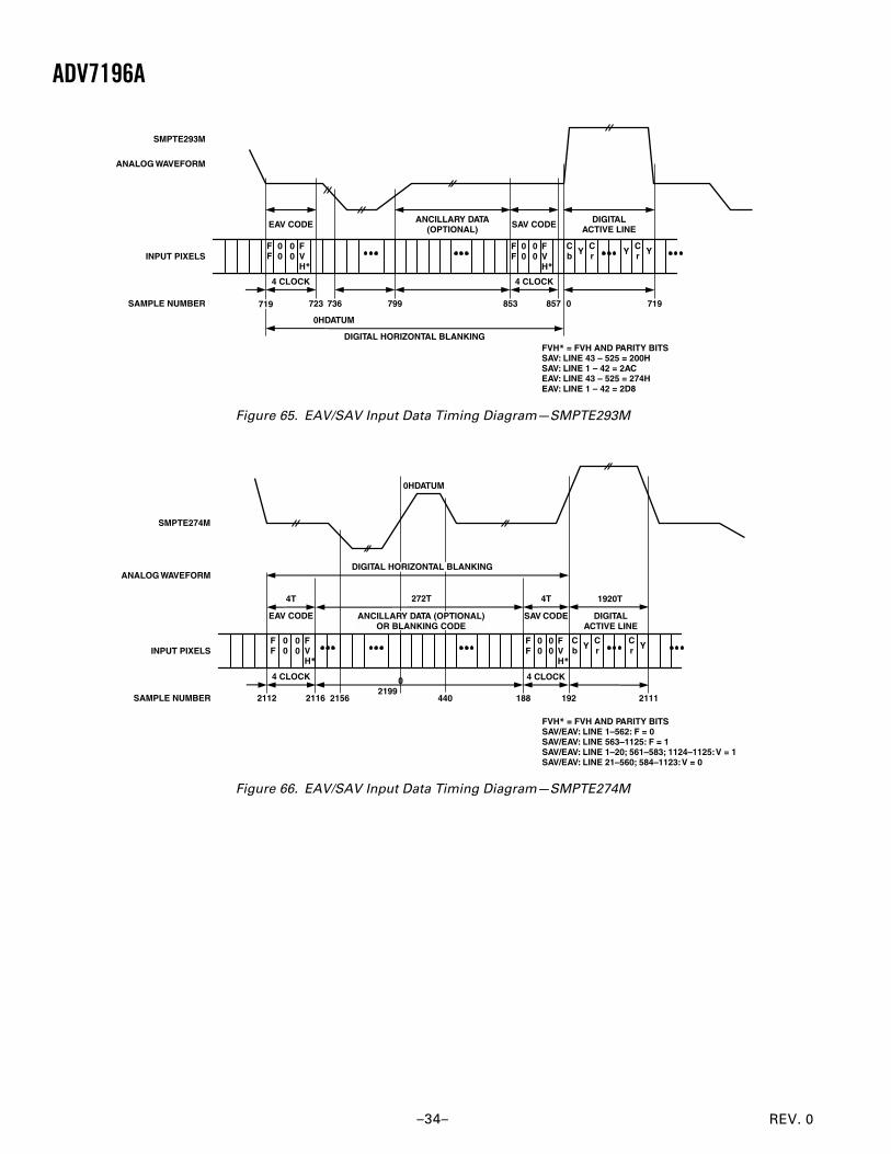
REV. 0
ADV7196A
–34–
FF
00INPUT PIXELS
00
FVH*
FF
00
FVH*
00
Cb Y
Cr Y
Cr Y
4 CLOCK
853799 857 0 719736723719
4 CLOCK
DIGITAL HORIZONTAL BLANKING
SAMPLE NUMBER
ANCILLARY DATA(OPTIONAL) SAV CODEEAV CODE DIGITAL
ACTIVE LINE
ANALOG WAVEFORM
SMPTE293M
0HDATUM
FVH* = FVH AND PARITY BITSSAV: LINE 43 – 525 = 200HSAV: LINE 1 – 42 = 2ACEAV: LINE 43 – 525 = 274HEAV: LINE 1 – 42 = 2D8
Figure 65. EAV/SAV Input Data Timing Diagram—SMPTE293M
FF
00INPUT PIXELS
00
FVH*
FF
00
FVH*
00
Cb Y
Cr
Cr Y
4 CLOCK
SAMPLE NUMBER
EAV CODE DIGITALACTIVE LINE
ANALOG WAVEFORM
SMPTE274M
4 CLOCK
2112 2116 21562199
440 188 192 2111
4T
SAV CODE
4T 1920T272T
ANCILLARY DATA (OPTIONAL)OR BLANKING CODE
DIGITAL HORIZONTAL BLANKING
0HDATUM
FVH* = FVH AND PARITY BITSSAV/EAV: LINE 1–562: F = 0SAV/EAV: LINE 563–1125: F = 1SAV/EAV: LINE 1–20; 561–583; 1124–1125: V = 1SAV/EAV: LINE 21–560; 584–1123: V = 0
0
Figure 66. EAV/SAV Input Data Timing Diagram—SMPTE274M
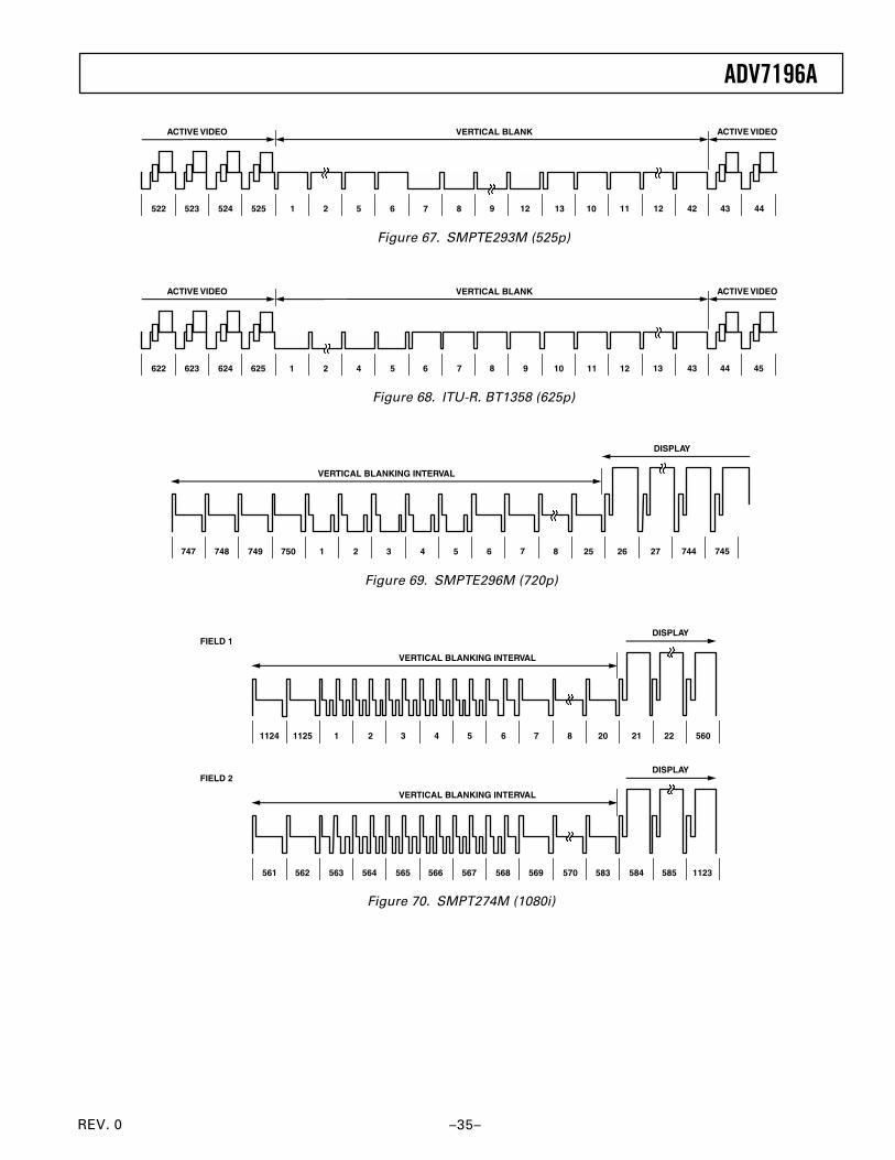
REV. 0
ADV7196A
–35–
522 523 524 525 1 2 5 6 7 8 9 12 13 10 11
ACTIVE VIDEO
12 42 43 44
ACTIVE VIDEOVERTICAL BLANK
Figure 67. SMPTE293M (525p)
622 623 624 625 1 2 4 5 6 7 8 9 10 11 12
ACTIVE VIDEO
13 43 44 45
ACTIVE VIDEOVERTICAL BLANK
Figure 68. ITU-R. BT1358 (625p)
747 748 749 750 1 2 3 4 5 6 7 8 25 26 27 744 745
DISPLAY
VERTICAL BLANKING INTERVAL
Figure 69. SMPTE296M (720p)
1124 1125 1 2 3 4 5 6 7 8 20 21 22 560
DISPLAY
VERTICAL BLANKING INTERVAL
FIELD 1
561 562 563 564 565 566 567 568 569 570 583 584 585 1123
DISPLAY
VERTICAL BLANKING INTERVAL
FIELD 2
Figure 70. SMPT274M (1080i)
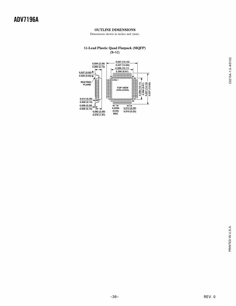
REV. 0
ADV7196A
–36–
52-Lead Plastic Quad Flatpack (MQFP)(S-52)
TOP VIEW(PINS DOWN)
1
1314
2726
394052
PIN 1
0.014 (0.35)0.010 (0.25)
0.557 (14.15)0.537 (13.65)0.398 (10.11)0.390 (9.91)
0.55
7 (1
4.15
)0.
537
(13.
65)
0.39
8 (1
0.11
)0.
390
(9.9
1)
0.0256(0.65)BSC
0.082 (2.09)0.078 (1.97)
0.012 (0.30)0.006 (0.15)0.008 (0.20)0.006 (0.15)
SEATINGPLANE
0.037 (0.95)0.026 (0.65)
0.094 (2.39)0.084 (2.13)
OUTLINE DIMENSIONSDimensions shown in inches and (mm).
C02
154–
1.5–
4/01
(0)
PR
INT
ED
IN U
.S.A
.