Embed Size (px)
Citation preview
5/14/2018 N Channel JFETs - slidepdf.com
http://slidepdf.com/reader/full/n-channel-jfets 1/6
J/SST201 SeriesVishay SiliconixNew Product
Document Number: 70233
S-03006—Rev. F, 17-Feb-03
www.vishay.com
6-1
N-Channel JFETs
J201 SST201
J202 SST202J204 SST204
PRODUCT SUMMARY
Part Number VGS(off) (V) V(BR)GSS Min (V) gfs Min (mS) IDSS Min (mA)
J/SST201 -0.3 to -1.5 -40 0.5 0.2
J/SST202 -0.8 to -4 -40 1 0.9
J/SST204 -0.3 to -2 -25 0.5 0.2
FEATURES BENEFITS APPLICATIONS
D Low Cutoff Voltage: J201 <1.5 V
DHigh Input Impedance
D Very Low Noise
D High Gain: AV = 80 @ 20 mA
D Full Performance from Low VoltagePower Supply: Down to 1.5 V
D Low Signal Loss/System Error
D High System Sensitivity
D High Quality Low-Level SignalAmplification
D High-Gain, Low-Noise Amplifiers
DLow-Current, Low-VoltageBattery-Powered Amplifiers
D Infrared Detector Amplifiers
D Ultra High Input ImpedancePre-Amplifiers
DESCRIPTION
The J/SST201 series features low leakage, very low noise,and low cutoff voltage for use with low-level power supplies.The J/SST201 is excellent for battery powered equipment andlow current amplifiers.
The J series, TO-226 (TO-92) plastic package, provides lowcost, while the SST series, TO-236 (SOT-23) package,provides surface-mount capabil ity. Both the J and SST series
are available in tape-and-reel for automated assembly (seePackaging Information).
For similar products in TO-206AA (TO-18) packaging, see the2N4338/4339/4340/4341 data sheet.
For applications information see AN102 and AN106.
TO-226AA(TO-92)
Top View
J201J202J204
D
G
S
1
2
3
D
S
G
TO-236(SOT-23)
2
3
1
Top View
SST201 (P1)*SST202 (P2)*SST204 (P4)*
*Marking Code for TO-236
5/14/2018 N Channel JFETs - slidepdf.com
http://slidepdf.com/reader/full/n-channel-jfets 2/6
J/SST201 Series
Vishay Siliconix New Product
www.vishay.com
6-2
Document Number: 70233
S-03006—Rev. F, 17-Feb-03
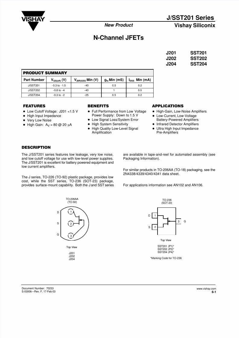
ABSOLUTE MAXIMUM RATINGS
Gate-Drain, Gate-Source Voltage -40 V. . . . . . . . . . . . . . . . . . . . . . . . . . . . . . .
Gate Current 50 mA. . . . . . . . . . . . . . . . . . . . . . . . . . . . . . . . . . . . . . . . . . . . . . . . .
Lead Temperature (1 / 16” from case for 10 sec.) 300_C. . . . . . . . . . . . . . . . . . .
Storage Temperature -55 to 150_C. . . . . . . . . . . . . . . . . . . . . . . . . . . . . . . . . . .
Operating Junction Temperature -55 to 150_C. . . . . . . . . . . . . . . . . . . . . . . . .
Power Dissipationa 350 mW. . . . . . . . . . . . . . . . . . . . . . . . . . . . . . . . . . . . . . . . .
Notesa. Derate 2.8 mW/ _C above 25_C
SPECIFICATIONS (T A = 25_C UNLESS OTHERWISE NOTED)
Limits
J/SST201 J/SST202 J/SST204c
Parameter Symbol Test Conditions Typa Min Max Min Max Min Max Unit
Static
Gate-SourceBreakdown Voltage
V(BR)GSS IG = - 1 mA , VDS = 0 V -40 -40 -25V
Gate-Source Cutoff Voltage VGS(off) VDS = 15 V, ID = 10 nA -0.3 -1.5 -0.8 -4 -0.3 -2
Saturation Drain Currentb IDSS VDS = 15 V, VGS = 0 V 0.2 1 0.9 4.5 0.2 3 mA
VGS = -20 V, VDS = 0 V -2 -100 -100 -100 pA
Gate Reverse Current IGSSTA = 125_C -1 nA
Gate Operating Current IG VDG = 10 V, ID = 0.1 mA -2
Drain Cutoff Current ID(off) VDS = 15 V, VGS = -5 V 2pA
Gate-Source Forward Voltage VGS(F) IG = 1 mA , VDS = 0 V 0.7 V
Dynamic
Common-SourceForward Transconductance
gfsVDS = 15 V, VGS = 0 V
f = 1 kHz0.5 1 0.5 mS
Common-SourceInput Capacitance
CissVDS = 15 V, VGS = 0 V
4.5
Common-SourceReverse Transfer Capacitance
Crss
,f = 1 MHz
1.3
pF
Equivalent Input Noise Voltage enVDS = 10 V, VGS = 0 V
f = 1 kHz6
nV ⁄ √Hz
Notesa. Typical values are for DESIGN AID ONLY, not guaranteed nor subject to production testing. NPA, NHb. Pulse test: PWv300 ms duty cyclev3%.c. See 2N/SST5484 Series for J204 typical characteristic curves.
5/14/2018 N Channel JFETs - slidepdf.com
http://slidepdf.com/reader/full/n-channel-jfets 3/6
J/SST201 SeriesVishay SiliconixNew Product
Document Number: 70233
S-03006—Rev. F, 17-Feb-03
www.vishay.com
6-3
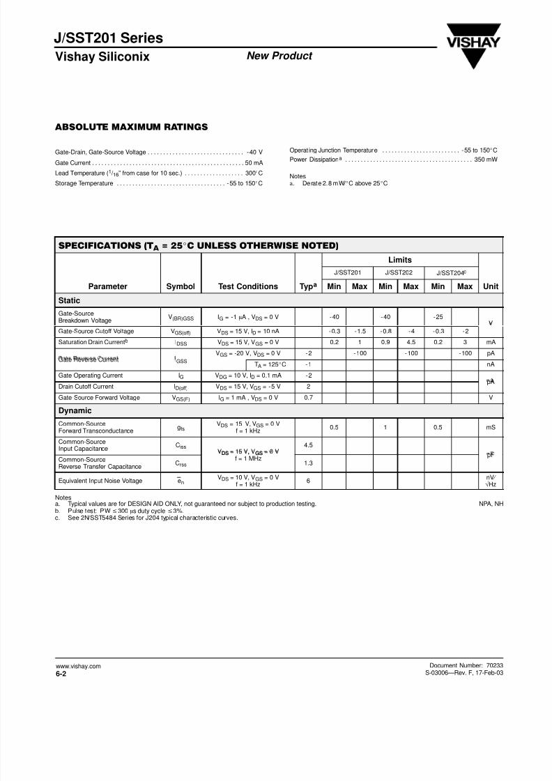
TYPICAL CHARACTERISTICS (T A = 25_C UNLESS OTHERWISE NOTED)
Gate Leakage Current
2
0 12 1684 20
1.6
1.2
0.8
0.4
0
Output Characteristics
VDS - Drain-Source Voltage (V)
VGS = 0 V
-0.6 V
-0.9 V
-0.3 V
VGS(off) = -1.5 V
-1.2 V
On-Resistance and Output Conductancevs. Gate-Source Cutoff Voltage
Drain Current and Transconductancevs. Gate-Source Cutoff Voltage
10
0.1 pA
1 pA
10 pA
100 pA
1 nA
10 nA
0 15 30
VDG - Drain-Gate Voltage (V)
IGSS @ 125_C
IGSS @ 25_C
TA = 125_C
TA = 25_C
ID = 100 mA
ID = 500 mA
IG @ ID = 500 mA
ID = 100 mA
0
8
6
4
2
0 -5-4-3-2-1
5
4
1
3
2
0
VGS(off) - Gate-Source Cutoff Voltage (V)
IDSS @ VDS = 10 V, VGS = 0 V
gfs @ VDS = 10 V, VGS = 0 Vf = 1 kHz
gfs
IDSS
1500
0 -3 -5-4-2-1
1200
900
600
300
0
0.01 0.1 1
2
1.6
0.8
0.4
0
10
8
4
2
0
400
0 12 164 20
360
160
80
0
Output Characteristics
Common-Source Forward Transconductancevs. Drain Current
ID - Drain Current (mA)VGS(off) - Gate-Source Cutoff Voltage (V)
VDS - Drain-Source Voltage (V)
TA = -55_C
125_C
-0.2 V
-0.4 V
-0.1 V
-0.3 V
rDS @ ID = 100 mA, VGS = 0 Vgos @ VDS = 10 V, VGS = 0 V, f = 1 kHz
rDS
gos
6 1.2
240
8
VGS(off) = -0.7 V
25_C
-0.5 V
VDS = 10 Vf = 1 kHz
VGS(off) = -1.5 V
VGS = 0 V
g o s - O u t p u t C on d u c t an c e ( m S )
I D S S
- S a t u r a t i o n D r a i n C u r r e n t ( m A )
r D S ( o n ) - D r a i n - S o u r c e O n - R e s i s t a n c e ( Ω )
g f s - F o r w a r d T r a n s c o n d u c t a n c e ( m S )
I D - D r a i n C u r r e n t (
m A )
I D - D r a i n C u r r e n t ( m A )
I G -
G a t e L e a k a g e ( A )
gf s
-F or w ar d T r an s c on d u c t an c e ( m S )
5/14/2018 N Channel JFETs - slidepdf.com
http://slidepdf.com/reader/full/n-channel-jfets 4/6
J/SST201 Series
Vishay Siliconix New Product
www.vishay.com
6-4
Document Number: 70233
S-03006—Rev. F, 17-Feb-03
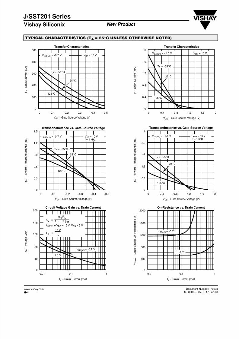
TYPICAL CHARACTERISTICS (T A = 25_C UNLESS OTHERWISE NOTED)
2
0 -1.2 -1.6 -2-0.8-0.4
1.6
1.2
0.8
0.4
0
Transfer Characteristics
VGS - Gate-Source Voltage (V)
TA = -55_C
125_C
25_C
VDS = 10 VVGS(off) = -1.5 V500
0 -0.3-0.2-0.1 -0.4 -0.5
400
300
200
100
0
Transfer Characteristics
VGS - Gate-Source Voltage (V)
TA = -55_C
125_C
25_C
VDS = 10 VVGS(off) = -0.7 V
0.1 10.01
4
-1.2 -2-1.6-0.8-0.40
3.2
2.4
1.6
0.8
0
0.01 0.1 1
200
160
120
80
40
0
2000
1600
1200
800
400
0
ID - Drain Current (mA)
Circuit Voltage Gain vs. Drain Current
Transconductance vs. Gate-Source Voltage
TA = -55_C
125_C
VGS - Gate-Source Voltage (V)
On-Resistance vs. Drain Current
ID - Drain Current (mA)
25_C
VGS(off) = -0.7 V
-1.5 VVGS(off) = -0.7 V
-1.5 V
1.5
0 -0.3 -0.4-0.2-0.1 -0.5
1.2
0.9
0.6
0.3
0
Transconductance vs. Gate-Source Voltage
TA = -55_C
125_C
VGS - Gate-Source Voltage (V)
25_C
VDS = 10 Vf = 1 kHz
VGS(off) = -0.7 V VDS = 10 Vf = 1 kHz
VGS(off) = -1.5 V
AV +
gfs RL
1 ) RLgos
Assume VDD = 15 V, VDS = 5 V
RL+
10 V
ID
g f s - F
o r w a r d T r a n s c o n d u c t a n c e ( m S )
g f s - F
o r w a r d T r a n s c o n d u c t a n c e ( m S )
r D S ( o n ) - D r a i n - S o u r c e O n - R e s i s t a n c e ( Ω )
I D - D r a i n C u r r e n t ( m A )
I D - D r a i n C u r r e n t ( m A )
A V
- V o l t a g e G a i n
5/14/2018 N Channel JFETs - slidepdf.com
http://slidepdf.com/reader/full/n-channel-jfets 5/6
J/SST201 SeriesVishay SiliconixNew Product
Document Number: 70233
S-03006—Rev. F, 17-Feb-03
www.vishay.com
6-5
TYPICAL CHARACTERISTICS (T A = 25_C UNLESS OTHERWISE NOTED)
Common-Source Input Capacitancevs. Gate-Source Voltage
10
0 -12 -16 -20-8-4
8
6
4
2
0
5
0 -12 -20-16-8-4
4
3
2
1
0
Common-Source Reverse Feedback Capacitancevs. Gate-Source Voltage
VGS - Gate-Source Voltage (V)
VDS = 0 V
10 V
f = 1 MHz
VGS - Gate-Source Voltage (V)
VDS = 0 V
10 V
f = 1 MHz
10 100 1 k 100 k10 k
20
16
12
8
4
0
Output Conductance vs. Drain Current
ID - Drain Current (mA)
TA = -55_C
125_C
Equivalent Input Noise Voltage vs. Frequency
f - Frequency (Hz)
VDS = 10 V
ID @ 100 mA
VGS = 0 V
3
2.4
1.8
0.8
0.4
0
0.01 0.1 1
25_C
Output Characteristics300
0 0.5
240
180
120
60
0
VDS - Drain-Source Voltage (V)
0.1 0.2 0.3 0.4
Output Characteristics1.0
0 1.0
0.8
0.6
0.4
0.2
0
VDS - Drain-Source Voltage (V)
0.2 0.4 0.6 0.8
VGS(off) = -0.7 VVGS = 0 V
-0.1
-0.2
-0.3
-0.4
-0.5
VGS(off) = -1.5 V
VGS = 0 V
-0.3
-0.6
-0.9
-1.2
VDS = 10 Vf = 1 kHz
VGS(off) = -1.5 V
e n
- N o i s e V o l t a g e
n V /
H z
I D - D r a i n C u r r e n
t ( m A )
I D - D r a i n C u r r e n
t ( µ A )
g o s
- O u t p u t C o n d u c t a n c e ( µ S )
C i s s - I n p u t C a p a c i t a n c e ( p F )
C r s s - R e v e r s e F e e d b a c k C a p a c i t a n c e ( p F
)

5/14/2018 N Channel JFETs - slidepdf.com
http://slidepdf.com/reader/full/n-channel-jfets 6/6
This datasheet has been download from:
www.datasheetcatalog.com
Datasheets for electronics components.


![FQP12N60C / FQPF12N60C 600V N-Channel · PDF fileFQP12N60C / FQPF12N60C 600V N-Channel MOSFET September 2007 QFET ... Case Temperature [ ]](https://img.pdfslide.net/doc/110x75/5aa9c8207f8b9a77188d4f43/fqp12n60c-fqpf12n60c-600v-n-channel-fqpf12n60c-600v-n-channel-mosfet-september.jpg)


![[SiC-En-2013-17] Challenges Regarding Parallel Connection of SiC JFETs](https://img.pdfslide.net/doc/110x75/577cda5a1a28ab9e78a57636/sic-en-2013-17-challenges-regarding-parallel-connection-of-sic-jfets.jpg)