Embed Size (px)
Citation preview

MEMS
NANO51
Foothill College


Overview
• What are MEMS/NEMS?
• History of MEMS
• Applications and examples
• Making MEMS
• Future of MEMS

What are MEMS/NEMS?
Acronym for:
MMicro EElectro MMechanical SSystems
NNano EElectro MMechanical SSystems
But what does this mean????
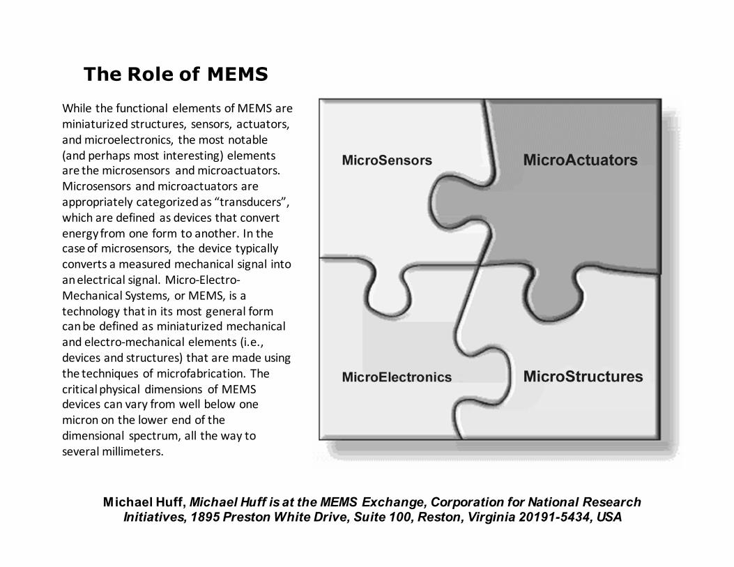
The Role of MEMS
While the functional elements of MEMS are
miniaturized structures, sensors, actuators,
and microelectronics, the most notable
(and perhaps most interesting) elements
are the microsensors and microactuators.
Microsensors and microactuators are
appropriately categorized as “transducers”,
which are defined as devices that convert
energy from one form to another. In the
case of microsensors, the device typically
converts a measured mechanical signal into
an electrical signal. Micro-Electro-
Mechanical Systems, or MEMS, is a
technology that in its most general form
can be defined as miniaturized mechanical
and electro-mechanical elements (i.e.,
devices and structures) that are made using
the techniques of microfabrication. The
critical physical dimensions of MEMS
devices can vary from well below one
micron on the lower end of the
dimensional spectrum, all the way to
several millimeters.
Michael Huff,Michael Huff is at the MEMS Exchange, Corporation for National Research Initiatives, 1895 Preston White Drive, Suite 100, Reston, Virginia 20191-5434, USA

MEMS – Smart Matter
• MEMS technology combines mechanical devices and electronics on a micro or nano scale
• Examples are sensors, valves, gears, mirrors, and actuators embedded in semiconductor chips.
• MEMS are sometimes referred to as smart matter.
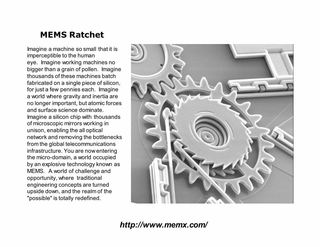
MEMS Ratchet
Imagine a machine so small that it is imperceptible to the human
eye. Imagine working machines no
bigger than a grain of pollen. Imagine
thousands of these machines batch
fabricated on a single piece of silicon, for just a few pennies each. Imagine
a world where gravity and inertia are
no longer important, but atomic forces
and surface science dominate.
Imagine a silicon chip with thousands of microscopic mirrors working in
unison, enabling the all optical
network and removing the bottlenecks
from the global telecommunications
infrastructure. You are now entering the micro-domain, a world occupied
by an explosive technology known as
MEMS. A world of challenge and
opportunity, where traditional
engineering concepts are turned upside down, and the realm of the
"possible" is totally redefined.
http://www.memx.com/
MEMS/NEMS
• Nanosystems and Micro-Electro-
Mechanical Systems (MEMS) are the
integration of mechanical elements,
sensors, actuators, and electronics on a
common silicon substrate through the
utilization of microfabrication
technology.

Foundational Technology
• Paul Saffo of the Institute for the Future
in Palo Alto, California, believes MEMS
or what he calls analog computing will
be "the foundational technology of the
next decade."

Other MEMS Terms
• Microengineering: the technologies and practice of making three dimensional structures and devices with dimensions in the order of micrometers.
• Micromachining: techniques used to produce the structures and moving parts of micro engineered devices
• Microsystems: The integration of microelectronic circuitry into micromachined structures, to produce completely systems
Source: Danny Banks http://www.dbanks.demon.co.uk

Micromachining/MEMS Applications
• Micro-sensors
– Light detectors, pressure sensors, strain gages,
temperature sensors7
• Micro-actuators
– Valves, gears, motors, resonators, cantilevers
• Structures
– Cavities, microneedles, fluidic channels, lenses,
membranes
• Lab-on-a-chip / micro-fluidics / diagnostics in
medicine / BioMEMS

What are Transducers?
A transducer is a medium for transforming
energy between 2 or more domains
A sensor measures something in its surrounding
environment and provides a response related to
the measured parameter
A mechanical actuator converts electrical signals
into a mechanical action
Source: Micromachined Transducers Sourcebook by Gregory Kovacs

MEMS Applications
• Automotive
• Telecommunications
• Sensors
• Actuators
• BioMEMS
http://www.memsnet.org/mems/applications.html

MEMS: Micromachines
As the name implies,
micromachines are very tiny
mechanisms. In fact, they are so
small that the unaided eye cannot
perceive them. Many different
types of professionals, such as
biologists, chemists, physicists,
and engineers, are involved in the
research and development of
these complex devices.
Micromachines can be a wide
variety of different mechanisms,
such as fluid channels, gears,
engines, tweezers, and mirrors -
all smaller than the width of a
human hair. So, what are these
micro-devices used for? Well,
many of them are creeping into
our everyday lives, in places
where you may not expect them.
http://webdocs.cs.ualberta.ca/~database/MEMS/sma_mems/mems.html

MEMS Sensors and Actuators(NTS: get pictures)
• Automotive Force, Pressure, Sound, and
Vibration
• Optical sensors (visible and IR / UV)
• Fluid flow (in micro environments)
• Industrial chemical and gas sensors
• Interfacing MEMS Sensors and Actuators
with Microcontrollers

Accelerometers
• NTS: get pictures and discuss how it
works
• MEMS accelerometers are used for air-
bag deployment in cars
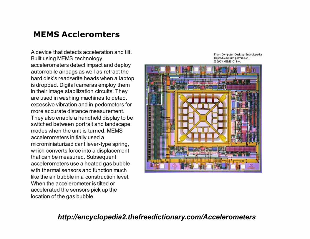
MEMS Accleromters
A device that detects acceleration and tilt. Built using MEMS technology,
accelerometers detect impact and deploy
automobile airbags as well as retract the
hard disk's read/write heads when a laptop
is dropped. Digital cameras employ them in their image stabilization circuits. They
are used in washing machines to detect
excessive vibration and in pedometers for
more accurate distance measurement.
They also enable a handheld display to be switched between portrait and landscape
modes when the unit is turned. MEMS
accelerometers initially used a
microminiaturized cantilever-type spring,
which converts force into a displacement that can be measured. Subsequent
accelerometers use a heated gas bubble
with thermal sensors and function much
like the air bubble in a construction level.
When the accelerometer is tilted or accelerated the sensors pick up the
location of the gas bubble.
http://encyclopedia2.thefreedictionary.com/Accelerometers

Microfabrica Accelerometer
The device at the bottom left with the C-shaped wings is an accelerometer. Built one metal layer at a time, Microfabrica's EFAB system was the first MEMS foundry
process to quickly turn customers' CAD files into micromachines. (Image courtesy
of Microfabrica Inc., www.microfabrica.com)
http://encyclopedia2.thefreedictionary.com/Accelerometers
More MEMS Pictures
• Gears
• Tweezers
• Springs
• Mirrors
• Cavities
• Comb drives
• Microneedles/tips

http://www.bacteria-world.com/mems-hinge.htm

BioMEMS Applications(NTS: get pictures)
• Lab-on-a-chip
• Micro fluidics
– DNA extraction / separation technology
– Protein separation / purification
– Electrophoresis, capillary flow measurements
• Biochips, microarrays, microsensors– In vivo diagnostic sensing
• ‘Smart-sensing’ in implantable devices

Bio-Microelectromechanical Systems
BYU BioMEMS research focuses on using microelectromechanical devices to move DNA and other molecules across biological cell boundaries. The effort uses a revolutionary
method based on nanoelectromechanical principles to place DNA inside of cells without
harming them. The research contributes to our understanding of many diseases, including
cancer, and has promise for future therapies for genetic disorders.

Computational MEMS
• Interfacing microcontrollers and MEMS
• Packaging issues of MEMS and CPU– interconnection reliability similar to standard
plastic IC packaging processes
– based on a standard flow for plastic packages
– applicable for a wide range of plastic packages (e.g. SOIC, QFP, PLCC, SSOP, BGA, CSP)
– can be applied with multi-chip concepts
– (sensors + ASIC)
– package cost for medium to high volumes

System on a Chip
http://www.genome.gov/pressDisplay.cfm?photoID=20017

Making MEMS

When does it make sense to Micromachine?
• Just because something can be built on
a micro or nano scale, doesn’t mean
that it should
• There has to be a significant advantage
over conventional designs

What are the Possible Advantages?
• Low cost from high volume fabrication (example: air bag sensors)
• Mechanical reliability
• Precise sensing techniques
• Access to areas/information where larger components can not reach
• Smaller components may provide convenience

Possible Disadvantages
• Lower tech solutions could be cheaper
• High development costs (motorization of R&D, packaging, and testing costs)
• Mechanical properties are different at the micro and macro scale
• Power supply may dwarf any advantages to smaller size
• Signal quality may be compromised at the microscale
• Thermal instability
• Difficulty in packaging
MEMS Materials / Environments
• Silicon technology
• Carbon based polymers
• Future working environments
– CNT integration
– Colloids / fluids
– Biological systems
– High pressure / reactive gas systems

MEMS Processing
Techniques
• Standard silicon technology (IC fab
techniques)
– Bulk micromachining
– Surface micromachining
• Polymers
• Electro Discharge Machining
• Molding
Micromachining
• Because silicon dominates the IC fabrication industry, it also dominates many of the fabrication techniques for nanotech forerunners such as MEMS and NEMS
• While the electronics are fabricated using IC process sequences, the micromechanical components are usually fabricated using compatible "micromachining" processes that selectively etch away parts of the silicon wafer or add new structural layers to form the mechanical and electromechanical devices

Bulk versus Surface Micromachining
• Bulk micromachining develops
structures by selectively etching a
silicon wafer
• Surface micromachining develops
structures by selectively adding thin
films and layers on the surface of a
silicon or other appropriate substrate

MEMS Processing
Techniques
• Deposition processes
• Lithography and photolithography
• Etching processes
• Surface treatments and coatings
• Packaging and CPU integration
• Metrology techniques for QA/QC
MEMS Application: Nanoindention for storage
• Discuss process to make,
• show end result, and
• what the advantages are and how it
would work
• Etc.

Current Trends and Future Directions in MEMS
• Downward cost pressure
• Increased / specialized functionality
• Integration in biological systems
• Integrating with CPUs / ASICS / RFID
• Mechanical ‘assembling’ functionality
– Rudimentary mechanical functioning
beyond simple sensors / actuators

MEMS Market Opportunities
• MEMS market size
– 2000 to 2005 (innovation)
– 2005 to 2010 (adoption / growth)
– 2010 to 2015 (maturation / mainstream)
– NTS: Get trend data

Challenges Facing MEMS
• Limits to silicon processing
– Three dimensions of exactness
– Cost and reliability of manufacturing
• Integration in biological systems
• Serviceability, design cycles
• Integration with CPUs / communications
• Needs an industry ‘sponsor’ (like RFID)
• PACKAGING

Micro-sensor
Micro-mirror Micro-gear
Micro-accelerometer
Self Assembly and Micro/Nano
Electronics

What are MEMS/NEMS?Micro-Electro-Mechanical Systems (MEMS) are the integration
of mechanical elements, sensors, actuators, and electronics on a
common silicon substrate through microfabrication technology.
Micro-sensor
Micro-mirror Micro-gear
Micro-accelerometer

MEMS vs. Integrated Circuits (IC’s)
• One way to look at it:
– IC’s move and sense electrons
– MEMS move and sense mass
• MEMS act as transducers (sensors) converting a
physical property into an electrical property (force to
voltage, etc…).
• MEMS can also actuate mechanical devices (switches,
mirrors, etc…)

• In the early 1980s Karlsruhe Nuclear
Research Center in Germany
developed LIGA
• LIGA is a German acronym for X-
ray lithography (X-ray
Lithographie), Electroplating
(Galvanoformung), and Molding
(Abformung)
• It allows for manufacturing of high
aspect ratio microstructures
• High aspect ratio structures are very
skinny and tall
• LIGA structures have precise
dimensions and good surface
roughness
Microfluidic device made using LIGA process
1982 LIGA Process Introduced1982 LIGA Process Introduced
Capacitive Comb drive also made using the LIGA process

• In 1986 IBM developed the atomic force microscope (AFM)
• The AFM maps the surface of an atomic structure
• Measures the force acting on the tip of a microscale cantilever
• It is a very high resolution type of scanning probe microscope with a resolution
of fractions of an Angstrom
1986 Invention of the AFM1986 Invention of the AFM

MEMS Applications
• Pressure Sensors
– Auto and Bio applications
• Ink Jet Print Heads
• Accelerometers
– (Inertial Sensors – “Crash Bags”, Navigation, Safety, iPhones)
• Micromachines
• Micro Fluidic Pumps
– Insulin Pump (drug delivery)
• Spatial Light Modulators (SLM’s)
– MOEM – Micro Optical Electro Mechanical Systems
– DMD – Digital Mirror Device
• Mass Storage Devices
• Chem Lab on a Chip
• Cantilever biosensors

MEMS Pressure Sensors
• Pressure Sensors
– Use piezoresistive silicon
sensors
– The silicon chip flexes as
pressure changes
– The amount the silicon
chip flexes determines the
output voltage signal.
These sensors help improve engine performance including gas mileage.

Pressure Sensors
TRW Commercial Gas Engine Sensor - 1985
Top view of the TRW (1985) pressure sensor, the metal components
are on top of the silicon membrane. The silicon membrane is
stressed when there is a pressure differential.

Intercardial catheter-tip sensors
These MEMS transducers are used in
intercardial catheter-tip sensors for
monitoring blood pressure during cardiac
catheterization.
Photo courtesy of Lucas NovaSensor, Fremont, CA.
0.15 x 0.4 x 0.9 mm

Disposable Blood Pressure SensorsDisposable sensors use MEMS transducers to measure changes in blood pressure.
Photo courtesy of Motorola, Sensor Products Div., Phoenix, AZ.
These $10 devices connect to a patient's
IV line and monitor blood pressure
through the IV solution.

This microphone is made from Silicon and is only
millimeters large. Photo Courtesy of EmKay
EmKay Sisonic Microphone

Ink JetInk jet printers are MEMS based – 1979 IBM and HP
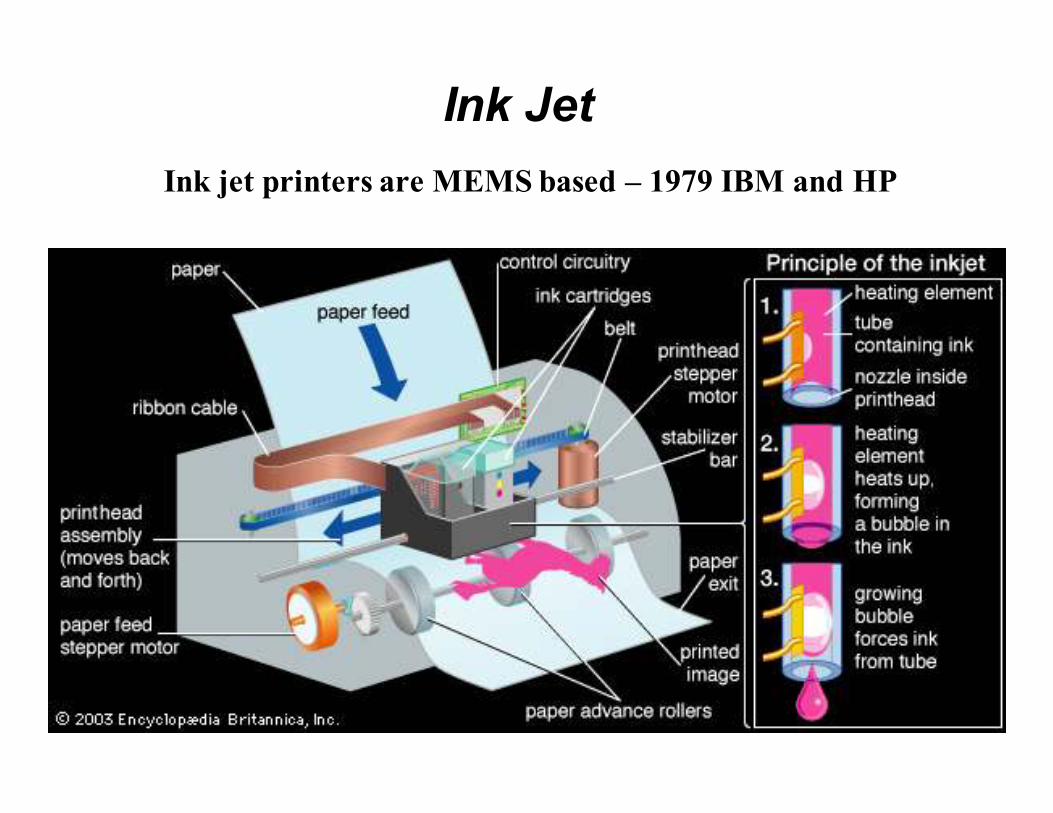
Ink jet printers are MEMS based – 1979 IBM and HP
Ink Jet

1979 HP Micromachined Inkjet Nozzle
Schematic of an array of inkjet
nozzles.
Close-up view of a
commercial inkjet printer
head illustrating the nozzles.This printing technique rapidly heats ink, creating tiny bubbles.
When the bubbles collapse, the ink squirts through an array of
nozzles onto paper and other media. Silicon micromachining
technology is used to manufacture the nozzles. The nozzles
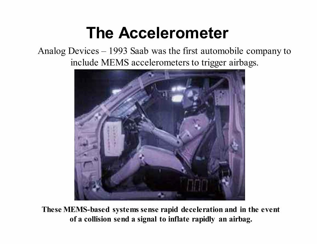
The AccelerometerAnalog Devices – 1993 Saab was the first automobile company to
include MEMS accelerometers to trigger airbags.
These MEMS-based systems sense rapid deceleration and in the event
of a collision send a signal to inflate rapidly an airbag.

The AccelerometerAn accelerometer is a sensor for testing the acceleration along a given axis.
The simplest MEMS accelerometer is an inertial mass suspended by springs.
Deflection of the mass is converted into an electrical signal.

iPhone
Nintendo Wii
IBM Thinkpad
http://www.youtube.com/watch?v=VmDnuqEOLps&feature=related
http://www.youtube.com/watch?v=Z24JP5TBnyE

The square in the middle of the chip is a resistor that heats up a gas
bubble. The next larger squares contain thermal couples that sense the
location of the heated bubble as the device is tilted or accelerated.
(Image courtesy of MEMSIC, Inc.)
MEMSIC's Dual-Axis Thermal Accelerator

MEMS as Machines
MEMS are often referred to as Micro Machines.
Tiny devices that move things.
Gear Train. Each gear tooth is
8 microns wide.
Mirror (popped up)

Micro Machines
• Surface Micromachining takes off in
the 1990’s.
• Sandia National Laboratories
This basically consists of alternating layers of structural materials (polycrystalline silicon) and
sacrificial layers (Silicon Dioxide). The sacrificial layer is a scaffold and acts as a temporary
support and spacing material. The last step of the process is the “release” step, where the
sacrificial layer is removed freeing the structural layers so they can move.
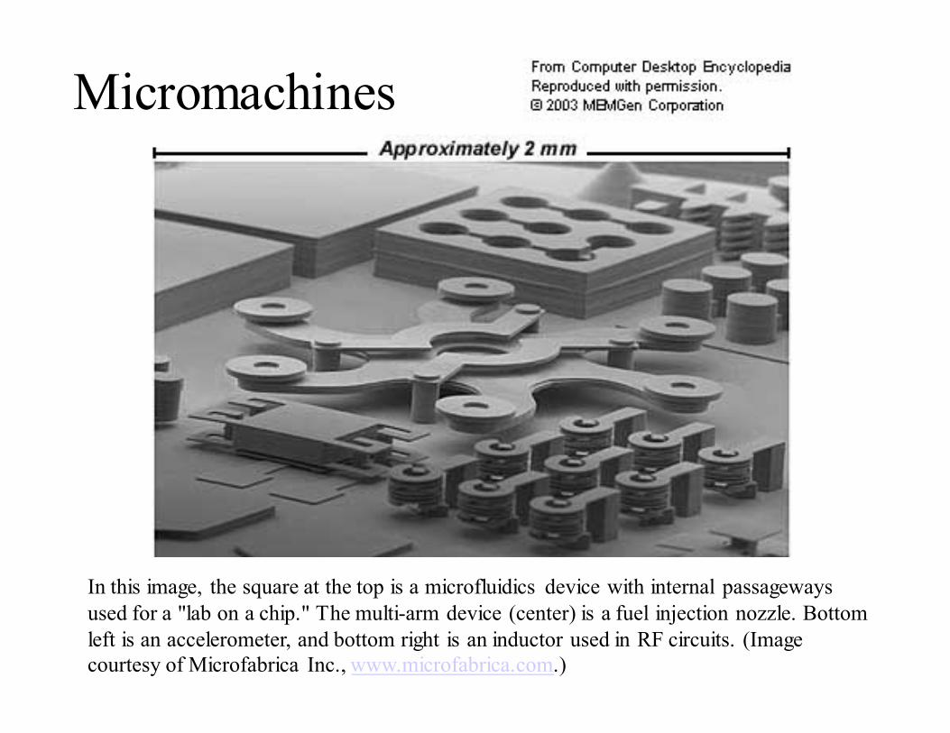
In this image, the square at the top is a microfluidics device with internal passageways
used for a "lab on a chip." The multi-arm device (center) is a fuel injection nozzle. Bottom
left is an accelerometer, and bottom right is an inductor used in RF circuits. (Image
courtesy of Microfabrica Inc., www.microfabrica.com.)
Micromachines

In this image, the square at the top is a microfluidics device with internal passageways
used for a "lab on a chip." The multi-arm device (center) is a fuel injection nozzle. Bottom
left is an accelerometer, and bottom right is an inductor used in RF circuits.
(Image courtesy of Microfabrica Inc., www.microfabrica.com.)
Micromachines
Microfluidics
Device

In this image, the square at the top is a microfluidics device with internal passageways
used for a "lab on a chip." The multi-arm device (center) is a fuel injection nozzle. Bottom
left is an accelerometer, and bottom right is an inductor used in RF circuits.
(Image courtesy of Microfabrica Inc., www.microfabrica.com.)
Micromachines
Fuel Injection
Nozzle
Microfluidics
Device

In this image, the square at the top is a microfluidics device with internal passageways
used for a "lab on a chip." The multi-arm device (center) is a fuel injection nozzle. Bottom
left is an accelerometer, and bottom right is an inductor used in RF circuits.
(Image courtesy of Microfabrica Inc., www.microfabrica.com.)
Micromachines
Accelerometer
Fuel Injection
Nozzle
Microfluidics
Device
Inducto
r

MEMS-based Optical Switch
These MEMS optical switches utilize micro mirrors to switch or reflect an
optical channel or signal from one location to another.
In 1999 Lucent Technologies developed the
first optical network switch
Micro Optical Electro Mechanical Systems (MOEMS)

Digital Mirror Device (DMD)
A DMD chip has on its surface several hundred thousand microscopic
mirrors which correspond to the pixels in the image to be displayed.
Digital Light Projector (DLP)

Digital Mirror Device (DMD)The mirrors can be individually rotated ±10-12°, to an on
or off state.

How Small are these Mirrors?
Each mirror is about 16µm square!
DMD mirrors – complete DLP units have over 2 million mirrors – all functioning!
Ant LegAnt Leg
Pin PointPin Point

Mass Storage - IBM
IBM’s “Millipede”
100 Tera Bit per square inch!
It works by making small indentations in a polymer
film.
Higher density data capability

Mass Storage - IBM
•A two-dimensional array of V-shaped silicon cantilevers, each 70
µm long.
•Writes divot into polymer by heating tip to 400°C
•Reads by looking at surface with 300°C tip (measures resistance
change with temp drop)
– if the tip is in a divot, the tip cools more than if it is not –
therefore, there is a change in resistivity which is measured by
the electronics.
•Erases by making an offset pit, which causes the nearby pit to
“pop up” and hence erases it.

BioMEMS
The overlap between microbiology and microsystem feature sizes
makes integration between the two possible
Atom
100 µm 10 µm 1 µm 0.1 µm 0.01 µm 0.001 µm
(1 nm)
Eukaryotic cells ProteinsVirusesBacteria
RibosomeNucleus
Gate of Leading
Edge Transistor
Visible Light
Surface Micromachining Features (MEMS)
Molecules
(10 nm)

Biomedical Applications
• Scientists are combining
sensors and actuators with
emerging biotechnology
• Applications include drug
delivery, DNA arrays, and
microfluidics
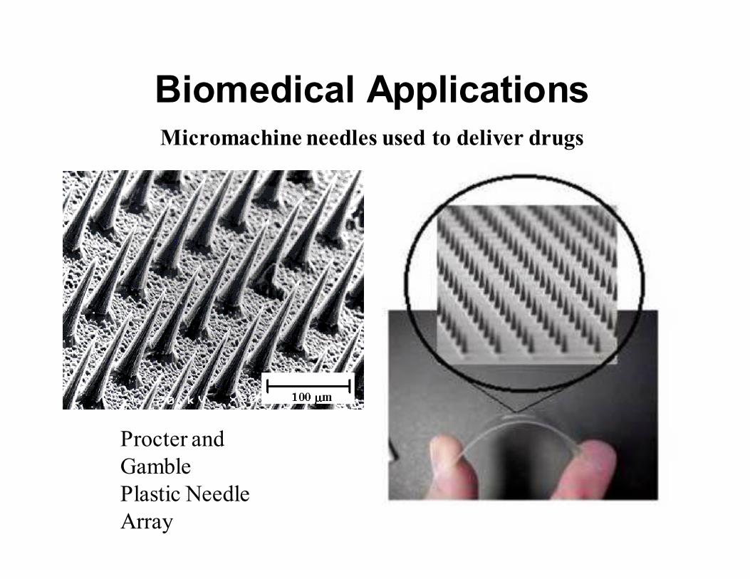
Biomedical ApplicationsMicromachine needles used to deliver drugs
Procter and
Gamble
Plastic Needle
Array
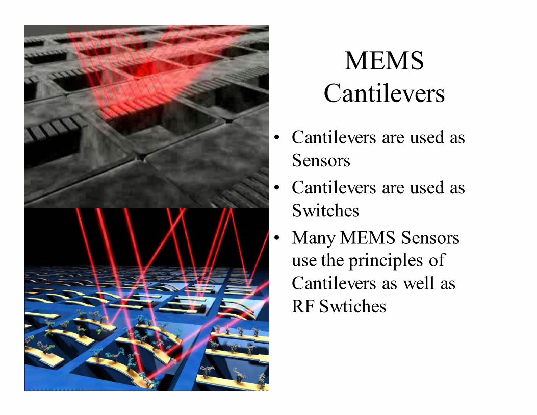
MEMS
Cantilevers
• Cantilevers are used as
Sensors
• Cantilevers are used as
Switches
• Many MEMS Sensors
use the principles of
Cantilevers as well as
RF Swtiches

What is a Cantilever?
Cantilevers have a resonant frequency that depends on the
length and the mass.

MEMS
Cantilever
sensors
• The ends of the cantilevers are coated with a layer of probe molecules.
• When a target molecule is present, it attaches to the probe molecule, thereby increasing the mass.
• The resonant frequency goes down.
• You just detected the presence of a molecule!

Cantilever Sensors
A gold dot, about 50 nanometers in diameter, fused to the end of a cantilevered
oscillator about 4 micrometers long.
A one-molecule-thick layer of a sulfur-containing chemical deposited on the gold
adds a mass of about 6 attograms (10-18 grams) , which is more than enough to
measure. Craighead Group/Cornell Univeristy
As mass is added to the cantilever shifts the resonance frequency.

Resonance Shift
5 x 15um Cantilever with an
E. Coli cell bound to
antibody layer.
Black is the response before cell attachment,
Red is after cell attachment.
School of Applied and Engineering Physics and the
Nanobiotechnology Center, Cornell University
http://www.news.cornell.edu/releases/April04/attograms.ws.html
Resonance Shift due to Single Cell

Resonance Frequency Shift as a
Function of Mass

Detection of Single DNA
http://www.hgc.cornell.edu/Nems%20Folder/Enumeration%20of%20Sin
gle%20DNA.html
By changing the coating
(Nano) one can functionalize
the cantilever to detect single
strands of DNA.
Mass resolution is on the
order of under 1 ato gram (10-
18grams)
Gold dot = 40nm
SiN thickness = 90nm

Future of MEMS
• Wireless / networked MEMS/BioMEMS
• Advanced biosensors / actuators
• Computational MEMS
• Advanced System on a Chip
• MEMS systems (networks of MEMS)

Summary
• What are MEMs?
• What do MEMs do?
• MEMs applications
• MEMs fabrication
• Future MEMs
– BioMEMS, NMEMS

MEMS References
• MEMS Clearinghouse -
http://www.memsnet.org/news/
• About MEMS – MEMX
http://www.memx.com/
• All about MEMS
http://www.allaboutmems.com/memsappli
cations-optical.html
• Sandia MEMS Homepage -
http://mems.sandia.gov/