Embed Size (px)
Citation preview
National Science and Technology Council Committee on TechnologyThe Interagency Working Group on Nanoscience, Engineering and Technology September 1999, Washington, D.C.
About the National Science and Technology Council
President Clinton established the National Science and Technology Council (NSTC) by ExecutiveOrder on November 23, 1993. This cabinet-level council is the principal means for the President tocoordinate science, space and technology policies across the Federal Government. NSTC acts as a“virtual” agency for science and technology (S&T) to coordinate the diverse parts of the Federalresearch and development (R&D) enterprise. The NSTC is chaired by the President. Membership con-sists of the Vice President, Assistant to the President for Science and Technology, CabinetSecretaries and Agency Heads with significant S&T responsibilities, and other White House officials.
An important objective of the NSTC is the establishment of clear national goals for Federal S&Tinvestments in areas ranging from information technologies and health research, to improving trans-portation systems and strengthening fundamental research. The Council prepares R&D strategiesthat are coordinated across Federal agencies to form an investment package that is aimed at accom-plishing multiple national goals.
To obtain additional information regarding the NSTC, contact 202-456-6100 or see the NSTC web site:http://www.whitehouse.gov/WH/EOP/OSTP/NSTC/html/NSTC_Home.html
Interagency Working Group on Nanoscience, Engineering and Technology (IWGN)
Chair: M.C. Roco, NSF.White House IWGN Co-chair: T.A. Kalil , Special Assistant to the President, WH Economic Council.Vice-chair: R. Trew, DOD.Executive Secretary: J.S. Murday, NRL.Members: K. Kirkpatrick (OSTP); J. Porter (NSTC), D. Radzanowski (OMB); P. Genther-Yoshida (DOC/TA); M.P. Casassa, R.D. Shull (DOC/NIST); G.S. Pomrenke (DOD/AFOSR);I.L. Thomas, R. Price, B.G. Volintine (DOE); R.R. John, A. Lacombe (DOT/Volpe Center); E. Murphy (DoTREAS); S. Venneri, G.H. Mucklow, M. Meyyappan, G. Krabach (NASA); J.A. Schloss, E. Kousvelari (NIH); T.A. Weber, M.P. Henkart (NSF).Public Affairs Consultant: J. Canton.
Acknowledgements:
Ivan Amato, WriterLiz Carroll, Design/LayoutGeoff Holdridge, Coordinator, WTEC Director, Loyola College
This report was prepared under the guidance of NSTC/CT. Any opinions, conclusions or recommendations expressed in this material are those of the authors, and do not necessarily reflect the views of the U.S. Government or individual funding agencies.
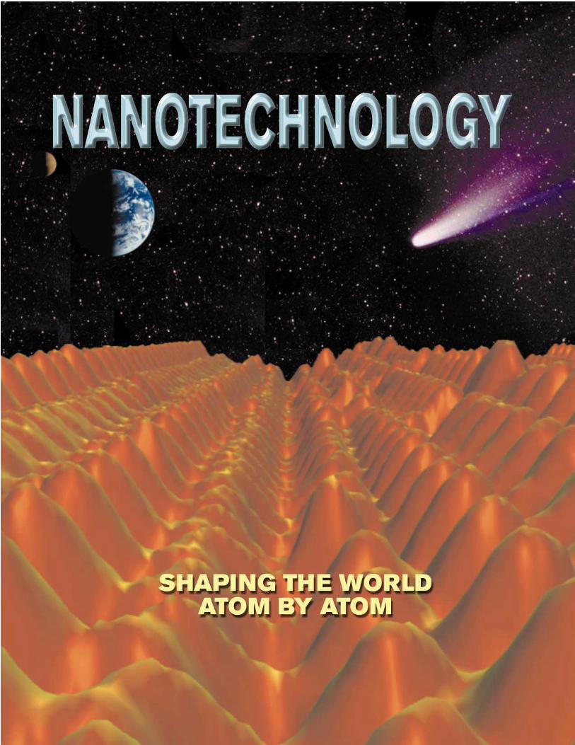
On the cover: This combination of a scanning tunneling micro-scope image of a siliconcrystal’s atomic sur-facescape with cosmicimagery evokes the vast-ness of nanoscience’spotential.
L. J
. W
hitm
an/N
aval
Res
earc
h La
bora
tory
.
f you were to deconstruct a humanbody into its most basic ingredients,
you’d get a little tank each of oxygen,hydrogen, and nitrogen. There would bepiddling piles of carbon, calcium, and salt.You’d squint at pinches of sulfur, phospho-rus, iron, and magnesium, and tiny dots of20 or so other chemical elements. Totalstreet value: not much.
With its own version of what scientistscall nanoengineering, nature transformsthese inexpensive, abundant, and inanimateingredients into self-generating, self-perpet-uating, self-repairing, self-aware creaturesthat walk, wiggle, swim, sniff, see, think,and even dream. Total value: immeasurable.
Now, a human brand of nanoengineer-ing is emerging. The field’s driving questionis this: What could we humans do if wecould assemble the basic ingredients of thematerial world with even a glint of nature’svirtuosity? What if we could build things theway nature does—atom by atom and mole-cule by molecule?
Scientists already are finding answers tothese questions. The more they learn, themore they suspect nanoscience and nano-engineering will become as socially trans-forming as the development of runningwater, electricity, antibiotics, and micro-electronics. The field is roughly where thebasic science and technology behind tran-sistors was in the late 1940s and 1950s.
In April 1998, Neal Lane, Assistant to the
President for Science and Technology andformer Director of the National ScienceFoundation (NSF), stated at a Congressionalhearing, “If I were asked for an area of sci-ence and engineering that will most likelyproduce the break-throughs of tomorrow, Iwould point tonanoscale science andengineering.”
Lane is not alone inthis view. Many scien-tists, including physicistand Nobel laureateHorst Stormer of LucentTechnologies andColumbia University,are themselves amazedthat the emerging nan-otechnology may pro-vide humanity withunprecedented controlover the material world.Says Stormer: “Nano-technology has given us the tools...to playwith the ultimate toy box of nature—atomsand molecules. Everything is made fromit...The possibilities to create new thingsappear limitless.”
So what do scientists like Lane andStormer mean by nanotechnology? In thelanguage of science, the prefix nanomeans one-billionth of something like asecond or a meter (see sidebar, p. 3).
Nanoscience and nanotechnology gener-ally refer to the world as it works on thenanometer scale, say, from one nanome-ter to several hundred nanometers. That’sthe natural spatial context for molecules
and their interactions,just as a 100 yard grid-iron is the relevantspatial context forfootball games. Nat-urally-occurring mole-cular players on thenanoscale field rangefrom tiny three-atomwater molecules tomuch larger proteinmolecules like oxy-gen-carrying hemo-globin with thousandsof atoms to giganticDNA molecules withmillions of atoms.Whenever scientistsand engineers push
their understanding and control over mat-ter to finer scales, as they now are doingon the nanoscale, they invariably discov-er qualitatively new phenomena andinvent qualitatively new technologies.“Nanotechnology is the builder's finalfrontier,” remarks Nobel laureate RichardSmalley, Rice University.
For years now, scientists have beendeveloping synthetic nanostructures that
1
Nanotechnology: Shaping The WorldAtom By Atom
The emerging fields of nanoscience and nanoengineering are leading to unprecedentedunderstanding and control over the fundamental building blocks of all physical things.
This is likely to change the way almost everything—from vaccines to computers to automobile tires to objects not yet imagined—is designed and made.
I
“If I were asked for anarea of science andengineering that willmost likely produce thebreakthroughs of tom-orrow, I would point tonanoscale science andengineering.”
–Neal LaneAssistant to the President
For Science and Technology
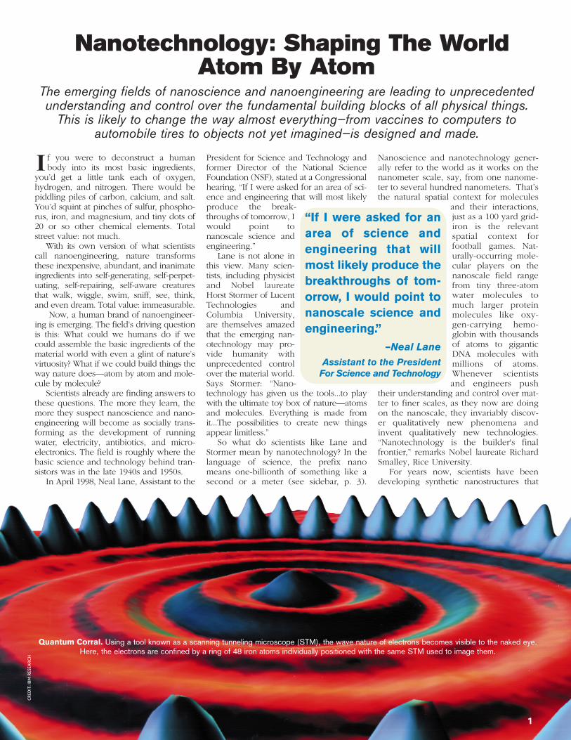
Quantum Corral. Using a tool known as a scanning tunneling microscope (STM), the wave nature of electrons becomes visible to the naked eye.Here, the electrons are confined by a ring of 48 iron atoms individually positioned with the same STM used to image them.
CR
ED
IT:I
BM
RES
EA
RC
H

2
could become the basis for countlessimproved and completely new technolo-gies. The way molecules of various shapesand surface features organize into patternson nanoscales determines importantmaterial properties, including electricalconductivity, optical properties, andmechanical strength. So by controllinghow that nanoscale patterning unfolds,researchers are learning to design newmaterials with new sets of properties.
Some of these nanostructures mayturn out to be useful as discrete nano-structures. New types of vaccines andmedicines come to mind here. Thevalue of others may emerge only asthey are assembled into larger struc-tures like particles or fibers, which thenwould be processed into yet largerstructures like textiles, films, coatings,bricks, and beams.
Forward looking researchersbelieve they could end up with syn-thetic creations with life-like behav-iors. Cover an airplane with paint con-taining nanoscale pigment particles thatinstantly reconfigure, chameleon-like, tomimic the aircraft’s surroundings. Youwould end up with an airplane indistin-guishable from the sky, that is, an invisi-ble plane. How about bricks and otherbuilding materials that can sense weatherconditions and then respond by alteringtheir inner structures to be more or lesspermeable to air and humidity? Thatwould go a long way toward improvingthe comfort and energy efficiency ofbuildings. And how about synthetic anti-body-like nanoscale drugs or devices thatmight seek out and destroy malignantcells wherever they might be in the body?
For many years futurists steeped in theculture of science fiction and prone tothinking in time frames that reach decadesahead have been dreaming up a fantasticfuture built using nanotechnologies. Morerecently, more cautious, establishedresearchers, who are developing the toolsand methods for a nanotechnologicalfuture, have been making projections oftheir own based on their expanding baseof knowledge and experience. “As weenter the 21st century, nanotechnology willhave a major impact on the health, wealthand security of the world’s people that willbe at least as significant in this century asantibiotics, the integrated circuit, and man-made polymers,” according to a committeeof leading scientists that convened inJanuary 1999 at the National ScienceFoundation to assess the potential roles ofnanotechnology in the coming years.
Not that it will be easy. Nanoscienceand nanoengineering remain in anexploratory phase. Scientists have yet tounderstand all of the scientific and engi-neering issues that define what can hap-pen and what can be done in the
nanoscale regime. Still, laboratory accom-plishments so far are making scientists inthis country and elsewhere bullish aboutthe future. So much so that the quest to
master the nanoscale is becoming a glob-al competition. New lightweight materialsfor future generations of more fuel effi-cient cars, military aircraft that can go far-ther and carry more payload, new classesof pharmaceuticals, materials that lastlonger and thereby reduce pollution frommanufacturing, are just a few of the goals.Companies and countries are experiment-ing with new organizational, industrialand budgetary models they hope willgive them the competitive edge towardthese ends.
The U.S. Government, for one, invest-ed approximately $116 million in fiscalyear 1997 in nanotechnology researchand development. For FY 1999, that fig-ure has risen to an estimated $260 mil-lion. Japan and Europe are making simi-lar investments. Whoever becomes mostknowledgeable and skilled on these
nanoscopic scales probably will findthemselves well positioned in the evermore technologically-based and global-ized economy of the 21st century.
That helps explain why the WhiteHouse National Science and Tech-nology Council (NSTC) created theInteragency Working Group onNanoscience, Engineering andTechnology (IWGN) in 1998. Withmembers from eight Federal agen-cies interacting closely with the aca-demic and industrial community, theIWGN’s charge has been to assessthe potential of nanotechnology andto formulate a national research anddevelopment plan. The Office ofScience and Technology Policy(OSTP) and the Office of Manage-ment and Budget (OMB) have sinceissued a joint memorandum toFederal agency heads that recom-mends nanotechnology as a researchpriority area for Federal investment
in FY 2001. The memorandum calls fora broad-based coalition in which acad-eme, the private sector, and local, state,and Federal governments work togetherto push the envelope of nanoscience andnanoengineering to reap nanotechnolo-gy’s potential social and economic bene-fits. The working group has recommend-ed a doubling of the annual investmentfor research in these areas to about a halfbillion dollars.
Some Deep Roots for a Nanotechnological Future
Nanotechnology is a new word, but it’snot an entirely new field. Chemical cataly-sis, which underlies a significant portion ofthe country’s gross national product, is anexample of “old nanotechnology.” Today,catalysts speed up thousands of chemicaltransformations like those that convert crude
oil into gasoline, small organicchemicals into life-saving drugsand polymers, and cheap graphiteinto synthetic diamond for makingindustrial cutting tools. They’reakin to biological catalysts—theenzymes in cells that orchestratethe chemistry of life. Most catalystswere discovered by trial anderror—by “shaking and baking”metals and ceramics and then see-ing how the result affects the reac-tions and their products. On closerexamination with modern tools,many of these catalysts turn out tobe highly organized metallicand/or ceramic nanostructureswhose specific architecturestrigger changes in molecules thattemporarily dock to them.Researchers expect this nanoscaleunderstanding of catalysis to lead
Natural nanotechnology: Much of the photosynthesisthat powers forests unfolds inside tiny cellular power hous-es called chloroplasts (above). These contain nanoscalemolecular machinery (including pigment molecules likechlorophyll) arranged inside stacked structures, called thy-lakoid disks, that convert light and carbon dioxide into bio-chemical energy.
1 micron
Inner membrane
Outermembrane
Thylakoiddisks
ILLU
ST
RA
TIO
N:L
IZ C
AR
RO
LL,A
DA
PT
ED
FR
OM
NA
NO
GEN
“Nanotechnology has given usthe tools...to play with the ulti-mate toy box of nature—atomsand molecules. Everything ismade from it...The possibilitiesto create new things appearlimitless.”
– Horst StormerLucent Technologies and
Columbia University,Physics Nobel Prize Winner
3
to better, cleaner, and more capable indus-trial processes.
Even an early instance of nanotechnol-ogy like catalysis really is young com-pared to nature’s own nanotechnology,which emerged billions of years agowhen molecules began organizing intothe complex structures that could supportlife. Photosynthesis, biology’s way of har-vesting the solar energy that runs so muchof the planet’s living kingdom, is one ofthose ancient products of evolution.Scientists often perceive photosynthesisas the result of brilliantly engineered mol-ecular ensembles—which include light-harvesting molecules such as chloro-phyll—arranged within cells on thenanometer and micrometer scales. Theseensembles capture light energy and con-vert it into the chemical energy (which isstored in chemical bonds) that drives thebiochemical machinery of plant cells.
The abalone, a mollusk, serves upanother perennial favorite in nature’sgallery of enviable nanotechnologies.These squishy creatures construct super-
tough shells with beautiful, iridescentinner surfaces. They do this by organizingthe same calcium carbonate of crumblyschoolroom chalk into tough nanostruc-tured bricks. For mortar, abalones concocta stretchy goo of protein and carbohy-drate. Cracks that may start on the outside
rarely make it all the way through; thestructure of the shell forces a crack to takea tortuous route around the tiny bricks,which dissipates the energy behind thedamage. Adding to the damage control isthat stretchy mortar. As a crack grows, themortar forms resilient nanostrings that tryto force any separating bricks backtogether. The result is a Lilliputian mason-ry that can withstand sharp beaks, teeth,even hammer blows.
This clever engineering of the abaloneshell reflects one of nanotechnology’smost enticing faces: by creating nanome-ter-scale structures, it’s possible to controlthe fundamental properties—like color,electrical conductivity, melting tempera-ture, hardness, crack-resistance, andstrength—of materials without changingthe materials’ chemical composition. Thestuff of soft chalk becomes hard shell.
Another feat of natural nanotechnolo-gy is in continuous operation every timeyou take a breath, move a muscle, liveanother second. Known antiseptically asF1-ATPase complexes, they’re actually
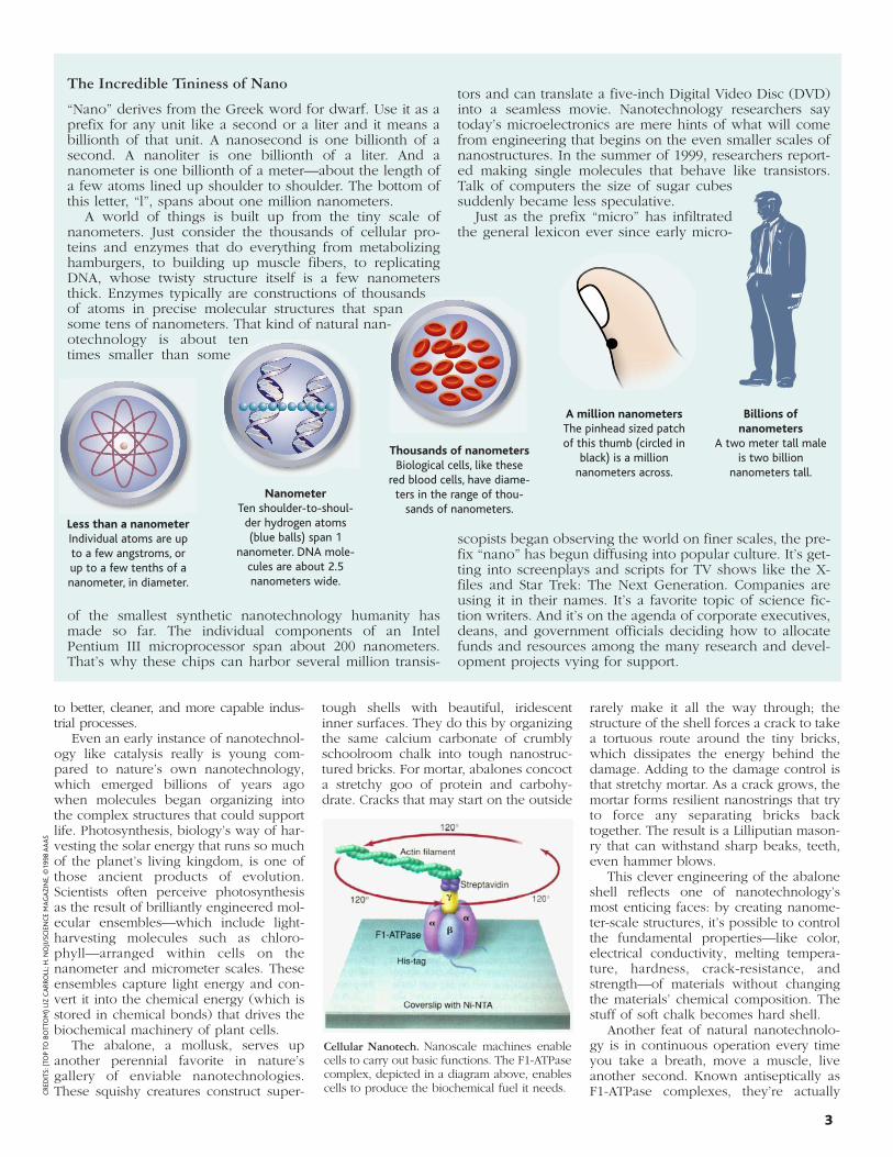
The Incredible Tininess of Nano
“Nano” derives from the Greek word for dwarf. Use it as aprefix for any unit like a second or a liter and it means abillionth of that unit. A nanosecond is one billionth of asecond. A nanoliter is one billionth of a liter. And ananometer is one billionth of a meter—about the length ofa few atoms lined up shoulder to shoulder. The bottom ofthis letter, “l”, spans about one million nanometers.
A world of things is built up from the tiny scale ofnanometers. Just consider the thousands of cellular pro-teins and enzymes that do everything from metabolizinghamburgers, to building up muscle fibers, to replicatingDNA, whose twisty structure itself is a few nanometersthick. Enzymes typically are constructions of thousandsof atoms in precise molecular structures that spansome tens of nanometers. That kind of natural nan-otechnology is about tentimes smaller than some
of the smallest synthetic nanotechnology humanity hasmade so far. The individual components of an IntelPentium III microprocessor span about 200 nanometers.That’s why these chips can harbor several million transis-
tors and can translate a five-inch Digital Video Disc (DVD)into a seamless movie. Nanotechnology researchers saytoday’s microelectronics are mere hints of what will comefrom engineering that begins on the even smaller scales ofnanostructures. In the summer of 1999, researchers report-ed making single molecules that behave like transistors.Talk of computers the size of sugar cubessuddenly became less speculative.
Just as the prefix “micro” has infiltratedthe general lexicon ever since early micro-
scopists began observing the world on finer scales, the pre-fix “nano” has begun diffusing into popular culture. It’s get-ting into screenplays and scripts for TV shows like the X-files and Star Trek: The Next Generation. Companies areusing it in their names. It’s a favorite topic of science fic-tion writers. And it’s on the agenda of corporate executives,deans, and government officials deciding how to allocatefunds and resources among the many research and devel-opment projects vying for support.
Less than a nanometer
Individual atoms are up
to a few angstroms, or
up to a few tenths of a
nanometer, in diameter.
Nanometer
Ten shoulder-to-shoul-
der hydrogen atoms
(blue balls) span 1
nanometer. DNA mole-
cules are about 2.5
nanometers wide.
Thousands of nanometers
Biological cells, like these
red blood cells, have diame-
ters in the range of thou-
sands of nanometers.
A million nanometers
The pinhead sized patch
of this thumb (circled in
black) is a million
nanometers across.
Billions of
nanometers
A two meter tall male
is two billion
nanometers tall.
Cellular Nanotech. Nanoscale machines enablecells to carry out basic functions. The F1-ATPasecomplex, depicted in a diagram above, enablescells to produce the biochemical fuel it needs.
CR
ED
ITS:(
TO
P T
O B
OT
TO
M)
LIZ
CA
RR
OLL
;H.N
OJI
/SC
IEN
CE M
AG
AZ
INE,©
19
98
AA
AS
CR
ED
IT:I
BM
RESEA
RC
H
4
molecular motors inside cells. Each ofthese motors is a complex of proteinsbound to the membranes of mitochon-dria, the cell’s bacteria-sized batteries.About 10 nanometers across, the F1-ATPase complexes are key players in thesynthesis of ATP—the molecular fuel forcellular activity. Scientists have found thatF1-ATPase complexes also generaterotary motion just like fan motorswhirring in summertime windows. Byattaching tiny protein filaments to thehub of F1-ATPase, researchers havevisualized this rotary action. And it setstheir own nanoengineering imaginationsinto motion with designs for human-made nanometer-scale machines.
Scientists using tools like electronmicroscopes to look at natural struc-tures like abalone shells and proteincomplexes hope to emulate some ofbiology’s nanoscale engineering. Theiraim is to create structural materials forstronger, lighter, more damage-resis-tant and otherwise better man-madeconstructions ranging from buildings
and cars to batteries and prosthetic limbs.From chalk to abalone shell . . . this is
the “alchemy” of natural nanotechnologywithout human intervention. And nowphysicists, chemists, materials scientists,biologists, mechanical and electrical engi-neers, and many other specialists arepooling their collective knowledge and
tools so that they too can tailor the worldon atomic and molecular scales. Abilitieslike this in the coming century couldmake the accomplishments of the 20thcentury seem quaint.
Even forty years ago, the physicistRichard Feynman envisioned a comingera of nanoscience and technology. In a
famous 1959 lecture titled,“There’s Plenty of Room atthe Bottom,” he outlinedwhat were then far-outpossibilities. They don’tseem quite so far-out any-more (see sidebar above).
What’s so Special About Nano
Nanotechnology stands outas a likely launch pad to anew technological erabecause it focuses on per-haps the final engineeringscales people have yet tomaster.
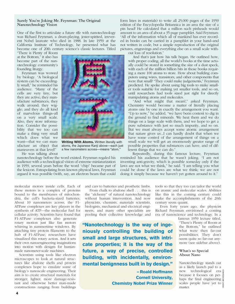
Surely You’re Joking Mr. Feynman: The Original Nanotechnology Vision
One of the first to articulate a future rife with nanotechnologywas Richard Feynman, a drum-playing, jester-spirited, irrever-ent Nobel laureate who died in 1988. In late 1959 at theCalifornia Institute of Technology, he presented what hasbecome one of 20th century science’s classic lectures. Titled“There is Plenty of Roomat the Bottom,” it also hasbecome part of the nan-otechnology community’sfounding liturgy.
Feynman was wowedby biology. “A biologicalsystem can be exceeding-ly small,” he reminded hisaudience. “Many of thecells are very tiny, butthey are active; they man-ufacture substances; theywalk around; they wig-gle; and they do all kindof marvelous things–allon a very small scale.Also, they store informa-tion. Consider the possi-bility that we too canmake a thing very smallwhich does what wewant—that we can man-ufacture an object thatmaneuvers at that level!”
He was talking aboutnanotechnology before the word existed. Feynman regaled hisaudience with a technological vision of extreme miniaturizationin 1959, several years before the word “chip” became part ofthe lexicon. Extrapolating from known physical laws, Feynmanargued it was possible (with, say, an electron beam that could
form lines in materials) to write all 25,000 pages of the 1959edition of the Encyclopedia Britannica in an area the size of apin head! He calculated that a million such pinheads wouldamount to an area of about a 35 page pamphlet. Said Feynman:“All of the information which all of mankind has ever record-ed in books can be carried in a pamphlet in your hand–andnot written in code, but a simple reproduction of the originalpictures, engravings and everything else on a small scale with-
out loss of resolution.”And that’s just how his talk began. He outlined how,
with proper coding, all the world’s books at the time actu-ally could be stored in something the size of a dust speck,with each of the million billion bits in those books requir-ing a mere 100 atoms to store. How about building com-puters using wires, transistors, and other components thatwere that small? “They could make judgements,” Feynmanpredicted. He spoke about using big tools to make small-er tools suitable for making yet smaller tools, and so on,until researchers had tools sized just right for directlymanipulating atoms and molecules.
“And what might that mean?,” asked Feynman.Chemistry would become a matter of literally placingatoms one by one in exactly the arrangement you want.“Up to now,” he added, “we have been content to dig inthe ground to find minerals. We heat them and we dothings on a large scale with them, and we hope to get apure substance with just so much impurity, and so on.But we must always accept some atomic arrangementthat nature gives us...I can hardly doubt that when wehave some control of the arrangement of things on asmall scale we will get an enormously greater range ofpossible properties that substances can have, and of dif-ferent things that we can do.”
Repeatedly, during this famous lecture, Feynmanreminded his audience that he wasn’t joking. “I am notinventing anti-gravity, which is possible someday only if thelaws are not what we think,” he said. “I am telling you whatcould be done if the laws are what we think; we are notdoing it simply because we haven’t yet gotten around to it.”
Writing With Atoms. Written literally withatoms, the Japanese Kanji above—each justa few nanometers across—means “atom.”
“Nanotechnology is the way of inge-niously controlling the building ofsmall and large structures, with intri-cate properties; it is the way of thefuture, a way of precise, controlledbuilding, with incidentally, environ-mental benignness built in by design.”
– Roald HoffmannCornell University,
Chemistry Nobel Prize Winner
CR
ED
ITS:(
TO
P T
O B
OT
TO
M)
HEW
LET
T-PA
CK
AR
D;R
ICH
AR
D S
IEG
EL
The pyramids in Egypt, the BrooklynBridge, and automobiles are conspicuousmonuments to how well and how longpeople have controlled matteron large scales of meters andmiles. The products of Swisswatchmakers even severalcenturies ago proved thathuman control over the mater-ial world had extended down-ward a thousandfold to themillimeter scale or so. Overthe past few decades,researchers have pushed thiscontrol down another hun-dredfold. Using microlitho-graphic techniques, they’velearned to inscribe silicon withultra-dense patterns of circuit-ry whose individual compo-nents now are only visiblewith powerful electron micro-scopes.
And all the while, chemistshave been learning to mix, blend, heat,react, and otherwise process chemicals toproduce millions of different specific mol-ecular structures. This is about the finestlevel of material structure relevant for mak-ing things. In so doing, researchers havedeveloped recipes and protocols for mak-ing the plastics, ceramics, semiconductors,metals, glass, fabrics, composites and othermaterials of the constructed landscape.
But there’s a big gap between the scaleof individual molecular structures madeby chemists and the the sub-microscopiccomponents on microprocessors made byelectrical engineers. That gap, whichspans from about one nanometer to sev-eral hundred nanometers, is where fun-damental properties are defined.
So with every advance researchersmake in nanotechnology, they stitchtogether an unbroken engineering nexusfrom atoms on up to skyscrapers. RoaldHoffmann, a chemist and Nobel Prizelaureate at Cornell University has put itthis way: “Nanotechnology is the way ofingeniously controlling the building ofsmall and large structures, with intricateproperties; it is the way of the future, away of precise, controlled building, withincidentally, environmental benignnessbuilt in by design.”
Going Quantum. Many researchers expectthat better control over the way atoms andmolecules assemble into tiny structurescould lead to a host of new technologiesbased on quantum phenomena thatbecome prevalent only at nanometer scales.
In the normal-sized realm of books,bricks, cars and houses, quantummechanics—the conceptual frameworkscientists use to describe and predict theproperties of matter on the levels ofatoms and electrons—doesn’t have much
direct relevance. As long as bricks holdup the house, who cares about theirquantum specifics? But now researchers
actually are creating nanoscale buildingblocks, such as metallic and ceramic par-ticles, and all-carbon “nanotubes,” thatare hundreds of millions of times smallerthan bricks used for houses and tubesused for plumbing. So scientists are find-ing themselves in the middle of quantummechanics territory.
In this nanoscale territory, electrons,for one, no longer flow through electricalconductors like rivers. On this scale, anelectron’s quantum mechanical natureexpresses itself as a wave. This behaviormakes it possible for electrons to doremarkable things, such as instantly tunnelthrough an insulating layer that normallywould have stopped it dead. The payoffof this behavior is that electronic devicesbuilt on nanoscales not only can packmore densely on a chip but also can oper-ate far faster—and with dramat-ically fewer electrons and lessenergy loss—than conventionaltransistors.
These characteristics ulti-mately could yield more power-ful computers that can help sci-entists mimic phenomena betterand engineers design productsbetter. In some speciallydesigned materials with nano-scale layers made of differentsemiconductor materials, elec-trons exhibit behaviors not pos-sible in less precisely organizedsettings. Researchers alreadyhave exploited this quantummechanical reality to designand build new solid state lasersthat emit light in wavelengthsgood for tasks like monitoringpollution, tracking chemicalreactions, and optical communi-cations.
What’s more, researchers already havetaken steps toward so-called quantum com-puters based on the energy states of atoms
and electrons. Theorists predictthat quantum computers, if theycan be realized, will be able tocalculate millions, even billions,of times faster than today’s super-computers. Nanotechnology maypropel early laboratory steps andtheoretical projections like thesetoward practical versions.
Surfaces Galore. Another majorfountain of new technology islikely to spout from a simple factof material reality: as objectsbecome smaller, the proportionof their constituent atoms at ornear the surface rises. Collectionsof very small particles, therefore,have high surface area comparedto their volume. This characteris-tic is profound because so much
of what happens in the world happens atsurfaces. Photosynthesis occurs on surfacesinside of cells. Catalysis happens on the sur-faces of particles. Ice in the atmosphereforms on the surfaces of floating dustspecks.
Smaller industrial catalysts, or ones withlabyrinthine interiors with nanoscale fea-tures, mean there’s more surface area forthousands of chemical transformations.Make a ceramic brick or a metal part, suchas a jet engine’s turbine blade, out ofnanoscale powder particles instead of con-ventional microscale powder particles andthe amount of internal surface goes up dra-matically. There’s no chemical differencebetween the two materials; only the size oftheir constituent particles differs. Yet, just forthat the nanostructured brick or metal piecemay be harder, less likely to crack, or
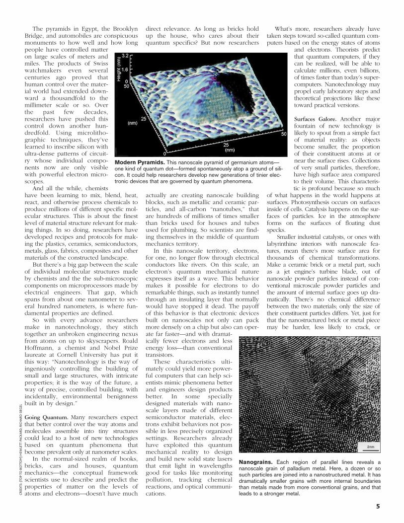
Modern Pyramids. This nanoscale pyramid of germanium atoms—one kind of quantum dot—formed spontaneously atop a ground of sili-con. It could help researchers develop new generations of tinier elec-tronic devices that are governed by quantum phenomena.
Nanograins. Each region of parallel lines reveals ananoscale grain of palladium metal. Here, a dozen or sosuch particles are joined into a nanostructured metal. It hasdramatically smaller grains with more internal boundariesthan metals made from more conventional grains, and thatleads to a stronger metal.
5
6
stronger at higher temperatures, than theconventional brick. That’s important for peo-ple who make things like armor or turbineblades for jet engines, which run more effi-ciently the hotter they become. The shift tonanoscale building blocks for making metal,ceramic, polymer and other material compo-nents is enabling researchers to “dial-in”many properties—like melting temperature,magnetic properties (e.g., the magneticdetection ability of materials in the readheads of hard disks), and color—that previ-ously were impossible to obtain for a partic-ular material.
Forty Years of Getting Around to It
Since Richard Feynman’s prescient lecture40 years ago about the opportunities har-bored in small scale engineering, thousandsof scientists have been developing theknowledge and means to intervene on thenanoscale. Now, human beings routinelysee and manipulate individual atoms andmolecules in their laboratories.
The tools and methods for making andtesting these diminutive objects havearcane names like scanning tunnelingmicroscopes, molecular beam epitaxy,and molecular self-assembly. Scientistsalso rely heavily on extremely powerfulcomputers to model and simulatenanoscale structures and phenomena.That helps them use their theories betterand to make sense of what they seethrough their microscopes. Simulationand modeling also help them evaluate theinfinite number of possible nanostruc-tures they could in principle try to build.Simulations can help steer researcherstoward fruitful directions and away fromdead ends. After all, on the nanoscale onemisplaced atom could make or break aquantum computer.
Here’s a sampling of some of the newtools available:
• Seeing Atoms. One of the biggest stepstoward nanoscale control was in 1981 when
researchers at IBM’s Research Center inSwitzerland—led by Gerd Binning andHeinrich Rohrer—told the world about theirscanning tunneling microscope, or STM. It’sessentially a superfine stylus that sweepsover a surface like a blind person’s walkingstick. But since the stylus is just a few atom-widths away and it has a molecularly or per-haps atomically fine tip, something quantummechanical happens. Electrons “tunnel”across the gap between the surface and thetip as the tip scans over the surface.
This technique enables a computer toconstruct fantastically enlarged images ofatomic or molecular landscapes normallyimpossible to see. The STM’s inventorsreceived a Nobel Prize because theirinvention quickly enabled thousands ofresearchers finally to “see” the atomic andmolecular landscapes of things.
So taken with the new view of thenanoworld STMs offered, scientists havedeveloped a raft of related instrumentsnow known collectively as scanningprobe microscopes (SPMs). Now, besidesSTM images of surface structures, scien-tists use SPMs like scanning tunnelingspectroscopes and near field scanningoptical microscopes to analyze the identi-ties of molecules andatoms on surfaces. Theyuse scanning thermalmicroscopes to see howheat travels on andthrough nanostructuressuch as solid-state lasers,made like a cake with tensor hundreds of nanoscalelayers of different semi-conductor materials. Theyuse scanning forcemicroscopy to examinemagnetic domains on stor-age media like hard disks.
• Moving Atoms. SPMs cando more than just peek inon previously hiddennanoscale environments.
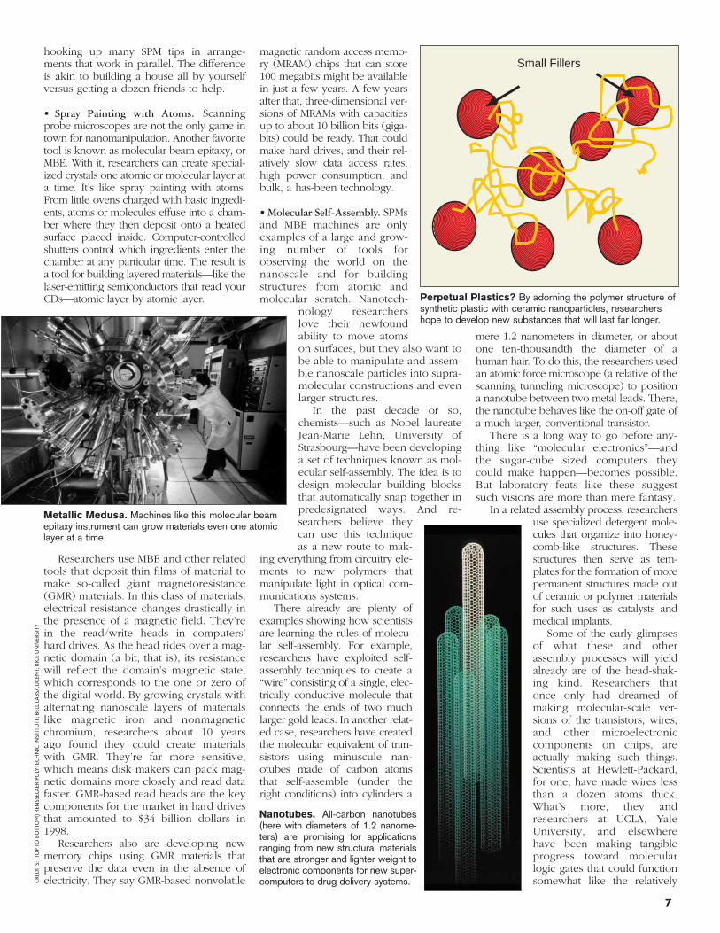
Donald Eigler of IBM’s Almaden ResearchCenter remembers the day in 1990 whenhe and Erhard K. Schweizer, who was vis-iting from the Fritz-Haber Institute inBerlin, moved individual atoms for thefirst time. In his laboratory notebookEigler used big letters and an exclamationmark to write THIS IS FUN! Using one ofthe most precise measuring and manipu-lating tools the world had ever seen, theresearchers slowly finessed 35 xenonatoms to spell out the three letter IBMlogo atop a crystal of nickel. To be sure,it only worked in a vacuum chamber keptat temperatures that make the North Poleseem tropical. But it was the kind of sub-microscopic manipulation that Feynmanwas talking about. The entire logospanned under three nanometers.
Since that feat, more researchers haveused STMs to create letters, pictures, as wellas exotic physical structures on surfaces oneatom at a time. And some researchers noware developing atom- and molecule-movingtools that are easier to use.
Consider a nanomanipulator that is beingdeveloped by a collaboration based at theUniversity of North Carolina, Chapel Hill.With it, people can manipulate nanostruc-tures in real time using what amounts to asophisticated joy stick that controls a scan-ning tunneling microscope. The developersof the system built it with force-feedback sooperators even “get a feel” for the atoms andmolecules they are moving. What’s more,the link between the joystick and the actualnanomanipulator is electronically mediated,which means it even can be controlled viathe Internet. Students in a nearby NorthCarolina high school used this nano-manipulator across the Internet to see, feeland modify individual virus particles.
These invaluable tools have openedmany new doors of discovery. But using asingle tip of a scanning probe microscopeeither for imaging or manipulating surfacesor tiny particles is painfully slow. In thepast few years, SPM developers have been
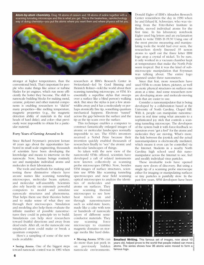
Atom-by-atom chemistry. Drag 18 atoms of cesium and 18 atoms of iodine together with ascanning tunneling microscope and this is what you get. This is the beakerless, nanotechnologyway of doing chemistry—you put the atoms where you want them and where physics will let you.
Smallest Writing. This famous set of images, now about 10years old, helped prove to the world that people indeed can moveatoms. The series shows how 35 atoms were moved to form afamous logo.
CR
ED
ITS:I
BM
RESEA
RC
H
CR
ED
ITS:(
TO
P T
O B
OT
TO
M)
REN
SSELA
ER
PO
LYT
EC
HN
IC I
NST
ITU
TE;B
ELL
LA
BS/L
UC
EN
T;R
ICE U
NIV
ER
SIT
Y
7
hooking up many SPM tips in arrange-ments that work in parallel. The differenceis akin to building a house all by yourselfversus getting a dozen friends to help.
• Spray Painting with Atoms. Scanningprobe microscopes are not the only game intown for nanomanipulation. Another favoritetool is known as molecular beam epitaxy, orMBE. With it, researchers can create special-ized crystals one atomic or molecular layer ata time. It’s like spray painting with atoms.From little ovens charged with basic ingredi-ents, atoms or molecules effuse into a cham-ber where they then deposit onto a heatedsurface placed inside. Computer-controlledshutters control which ingredients enter thechamber at any particular time. The result isa tool for building layered materials—like thelaser-emitting semiconductors that read yourCDs—atomic layer by atomic layer.
Researchers use MBE and other relatedtools that deposit thin films of material tomake so-called giant magnetoresistance(GMR) materials. In this class of materials,electrical resistance changes drastically inthe presence of a magnetic field. They’rein the read/write heads in computers’hard drives. As the head rides over a mag-netic domain (a bit, that is), its resistancewill reflect the domain’s magnetic state,which corresponds to the one or zero ofthe digital world. By growing crystals withalternating nanoscale layers of materialslike magnetic iron and nonmagneticchromium, researchers about 10 yearsago found they could create materialswith GMR. They’re far more sensitive,which means disk makers can pack mag-netic domains more closely and read datafaster. GMR-based read heads are the keycomponents for the market in hard drivesthat amounted to $34 billion dollars in1998.
Researchers also are developing newmemory chips using GMR materials thatpreserve the data even in the absence ofelectricity. They say GMR-based nonvolatile
magnetic random access memo-ry (MRAM) chips that can store100 megabits might be availablein just a few years. A few yearsafter that, three-dimensional ver-sions of MRAMs with capacitiesup to about 10 billion bits (giga-bits) could be ready. That couldmake hard drives, and their rel-atively slow data access rates,high power consumption, andbulk, a has-been technology.
• Molecular Self-Assembly. SPMsand MBE machines are onlyexamples of a large and grow-ing number of tools forobserving the world on thenanoscale and for buildingstructures from atomic andmolecular scratch. Nanotech-
nology researcherslove their newfoundability to move atomson surfaces, but they also want tobe able to manipulate and assem-ble nanoscale particles into supra-molecular constructions and evenlarger structures.
In the past decade or so,chemists—such as Nobel laureateJean-Marie Lehn, University ofStrasbourg—have been developinga set of techniques known as mol-ecular self-assembly. The idea is todesign molecular building blocksthat automatically snap together inpredesignated ways. And re-searchers believe theycan use this techniqueas a new route to mak-
ing everything from circuitry ele-ments to new polymers thatmanipulate light in optical com-munications systems.
There already are plenty ofexamples showing how scientistsare learning the rules of molecu-lar self-assembly. For example,researchers have exploited self-assembly techniques to create a“wire” consisting of a single, elec-trically conductive molecule thatconnects the ends of two muchlarger gold leads. In another relat-ed case, researchers have createdthe molecular equivalent of tran-sistors using minuscule nan-otubes made of carbon atomsthat self-assemble (under theright conditions) into cylinders a
mere 1.2 nanometers in diameter, or aboutone ten-thousandth the diameter of ahuman hair. To do this, the researchers usedan atomic force microscope (a relative of thescanning tunneling microscope) to positiona nanotube between two metal leads. There,the nanotube behaves like the on-off gate ofa much larger, conventional transistor.
There is a long way to go before any-thing like “molecular electronics”—andthe sugar-cube sized computers theycould make happen—becomes possible.But laboratory feats like these suggestsuch visions are more than mere fantasy.
In a related assembly process, researchersuse specialized detergent mole-cules that organize into honey-comb-like structures. Thesestructures then serve as tem-plates for the formation of morepermanent structures made outof ceramic or polymer materialsfor such uses as catalysts andmedical implants.
Some of the early glimpsesof what these and otherassembly processes will yieldalready are of the head-shak-ing kind. Researchers thatonce only had dreamed ofmaking molecular-scale ver-sions of the transistors, wires,and other microelectroniccomponents on chips, areactually making such things.Scientists at Hewlett-Packard,for one, have made wires lessthan a dozen atoms thick.What’s more, they andresearchers at UCLA, YaleUniversity, and elsewherehave been making tangibleprogress toward molecularlogic gates that could functionsomewhat like the relatively
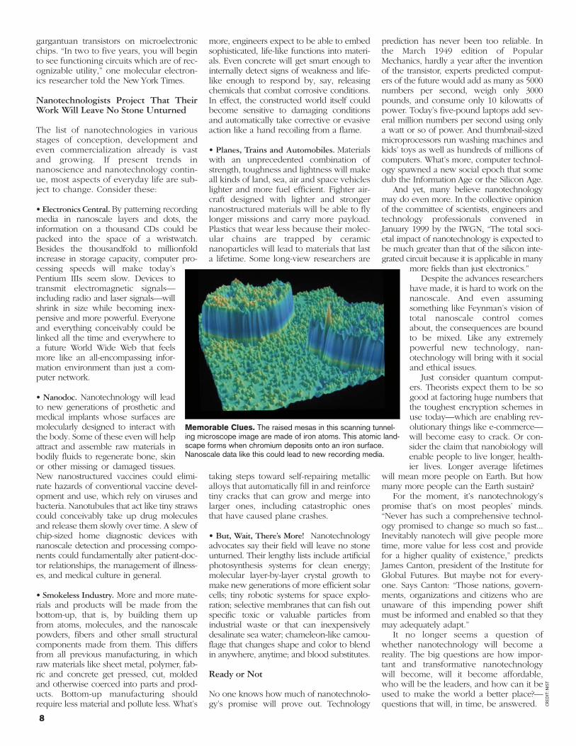
Metallic Medusa. Machines like this molecular beamepitaxy instrument can grow materials even one atomiclayer at a time.
Small Fillers
Perpetual Plastics? By adorning the polymer structure ofsynthetic plastic with ceramic nanoparticles, researchershope to develop new substances that will last far longer.
Nanotubes. All-carbon nanotubes(here with diameters of 1.2 nanome-ters) are promising for applicationsranging from new structural materialsthat are stronger and lighter weight toelectronic components for new super-computers to drug delivery systems.
CR
ED
IT:N
IST
8
gargantuan transistors on microelectronicchips. “In two to five years, you will beginto see functioning circuits which are of rec-ognizable utility,” one molecular electron-ics researcher told the New York Times.
Nanotechnologists Project That TheirWork Will Leave No Stone Unturned
The list of nanotechnologies in variousstages of conception, development andeven commercialization already is vastand growing. If present trends innanoscience and nanotechnology contin-ue, most aspects of everyday life are sub-ject to change. Consider these:
• Electronics Central. By patterning recordingmedia in nanoscale layers and dots, theinformation on a thousand CDs could bepacked into the space of a wristwatch.Besides the thousandfold to millionfoldincrease in storage capacity, computer pro-cessing speeds will make today’sPentium IIIs seem slow. Devices totransmit electromagnetic signals—including radio and laser signals—willshrink in size while becoming inex-pensive and more powerful. Everyoneand everything conceivably could belinked all the time and everywhere toa future World Wide Web that feelsmore like an all-encompassing infor-mation environment than just a com-puter network.
• Nanodoc. Nanotechnology will leadto new generations of prosthetic andmedical implants whose surfaces aremolecularly designed to interact withthe body. Some of these even will helpattract and assemble raw materials inbodily fluids to regenerate bone, skinor other missing or damaged tissues.New nanostructured vaccines could elimi-nate hazards of conventional vaccine devel-opment and use, which rely on viruses andbacteria. Nanotubules that act like tiny strawscould conceivably take up drug moleculesand release them slowly over time. A slew ofchip-sized home diagnostic devices withnanoscale detection and processing compo-nents could fundamentally alter patient-doc-tor relationships, the management of illness-es, and medical culture in general.
• Smokeless Industry. More and more mate-rials and products will be made from thebottom-up, that is, by building them upfrom atoms, molecules, and the nanoscalepowders, fibers and other small structuralcomponents made from them. This differsfrom all previous manufacturing, in whichraw materials like sheet metal, polymer, fab-ric and concrete get pressed, cut, moldedand otherwise coerced into parts and prod-ucts. Bottom-up manufacturing shouldrequire less material and pollute less. What’s
more, engineers expect to be able to embedsophisticated, life-like functions into materi-als. Even concrete will get smart enough tointernally detect signs of weakness and life-like enough to respond by, say, releasingchemicals that combat corrosive conditions.In effect, the constructed world itself couldbecome sensitive to damaging conditionsand automatically take corrective or evasiveaction like a hand recoiling from a flame.
• Planes, Trains and Automobiles. Materialswith an unprecedented combination ofstrength, toughness and lightness will makeall kinds of land, sea, air and space vehicleslighter and more fuel efficient. Fighter air-craft designed with lighter and strongernanostructured materials will be able to flylonger missions and carry more payload.Plastics that wear less because their molec-ular chains are trapped by ceramicnanoparticles will lead to materials that lasta lifetime. Some long-view researchers are
taking steps toward self-repairing metallicalloys that automatically fill in and reinforcetiny cracks that can grow and merge intolarger ones, including catastrophic onesthat have caused plane crashes.
• But, Wait, There’s More! Nanotechnologyadvocates say their field will leave no stoneunturned. Their lengthy lists include artificialphotosynthesis systems for clean energy;molecular layer-by-layer crystal growth tomake new generations of more efficient solarcells; tiny robotic systems for space explo-ration; selective membranes that can fish outspecific toxic or valuable particles fromindustrial waste or that can inexpensivelydesalinate sea water; chameleon-like camou-flage that changes shape and color to blendin anywhere, anytime; and blood substitutes.
Ready or Not
No one knows how much of nanotechnolo-gy’s promise will prove out. Technology
prediction has never been too reliable. Inthe March 1949 edition of PopularMechanics, hardly a year after the inventionof the transistor, experts predicted comput-ers of the future would add as many as 5000numbers per second, weigh only 3000pounds, and consume only 10 kilowatts ofpower. Today’s five-pound laptops add sev-eral million numbers per second using onlya watt or so of power. And thumbnail-sizedmicroprocessors run washing machines andkids’ toys as well as hundreds of millions ofcomputers. What’s more, computer technol-ogy spawned a new social epoch that somedub the Information Age or the Silicon Age.
And yet, many believe nanotechnologymay do even more. In the collective opinionof the committee of scientists, engineers andtechnology professionals convened inJanuary 1999 by the IWGN, “The total soci-etal impact of nanotechnology is expected tobe much greater than that of the silicon inte-grated circuit because it is applicable in many
more fields than just electronics.” Despite the advances researchers
have made, it is hard to work on thenanoscale. And even assumingsomething like Feynman’s vision oftotal nanoscale control comesabout, the consequences are boundto be mixed. Like any extremelypowerful new technology, nan-otechnology will bring with it socialand ethical issues.
Just consider quantum comput-ers. Theorists expect them to be sogood at factoring huge numbers thatthe toughest encryption schemes inuse today—which are enabling rev-olutionary things like e-commerce—will become easy to crack. Or con-sider the claim that nanobiology willenable people to live longer, health-ier lives. Longer average lifetimes
will mean more people on Earth. But howmany more people can the Earth sustain?
For the moment, it’s nanotechnology’spromise that’s on most peoples’ minds.“Never has such a comprehensive technol-ogy promised to change so much so fast...Inevitably nanotech will give people moretime, more value for less cost and providefor a higher quality of existence,” predictsJames Canton, president of the Institute forGlobal Futures. But maybe not for every-one. Says Canton: “Those nations, govern-ments, organizations and citizens who areunaware of this impending power shiftmust be informed and enabled so that theymay adequately adapt.”
It no longer seems a question ofwhether nanotechnology will become areality. The big questions are how impor-tant and transformative nanotechnologywill become, will it become affordable,who will be the leaders, and how can it beused to make the world a better place?—questions that will, in time, be answered.
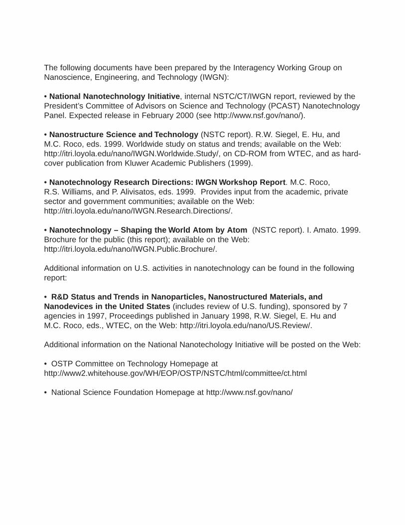
Memorable Clues. The raised mesas in this scanning tunnel-ing microscope image are made of iron atoms. This atomic land-scape forms when chromium deposits onto an iron surface.Nanoscale data like this could lead to new recording media.
The following documents have been prepared by the Interagency Working Group onNanoscience, Engineering, and Technology (IWGN):
• National Nanotechnology Initiative , internal NSTC/CT/IWGN report, reviewed by thePresident’s Committee of Advisors on Science and Technology (PCAST) NanotechnologyPanel. Expected release in February 2000 (see http://www.nsf.gov/nano/).
• Nanostructure Science and Technology (NSTC report). R.W. Siegel, E. Hu, andM.C. Roco, eds. 1999. Worldwide study on status and trends; available on the Web:http://itri.loyola.edu/nano/IWGN.Worldwide.Study/, on CD-ROM from WTEC, and as hard-cover publication from Kluwer Academic Publishers (1999).
• Nanotechnology Research Directions: IWGN Workshop Report . M.C. Roco,R.S. Williams, and P. Alivisatos, eds. 1999. Provides input from the academic, privatesector and government communities; available on the Web:http://itri.loyola.edu/nano/IWGN.Research.Directions/.
• Nanotechnology – Shaping the World Atom by Atom (NSTC report). I. Amato. 1999.Brochure for the public (this report); available on the Web:http://itri.loyola.edu/nano/IWGN.Public.Brochure/.
Additional information on U.S. activities in nanotechnology can be found in the followingreport:
• R&D Status and Trends in Nanoparticles, Nanostructured Materials, andNanodevices in the United States (includes review of U.S. funding), sponsored by 7agencies in 1997, Proceedings published in January 1998, R.W. Siegel, E. Hu andM.C. Roco, eds., WTEC, on the Web: http://itri.loyola.edu/nano/US.Review/.
Additional information on the National Nanotechology Initiative will be posted on the Web:
• OSTP Committee on Technology Homepage athttp://www2.whitehouse.gov/WH/EOP/OSTP/NSTC/html/committee/ct.html
• National Science Foundation Homepage at http://www.nsf.gov/nano/
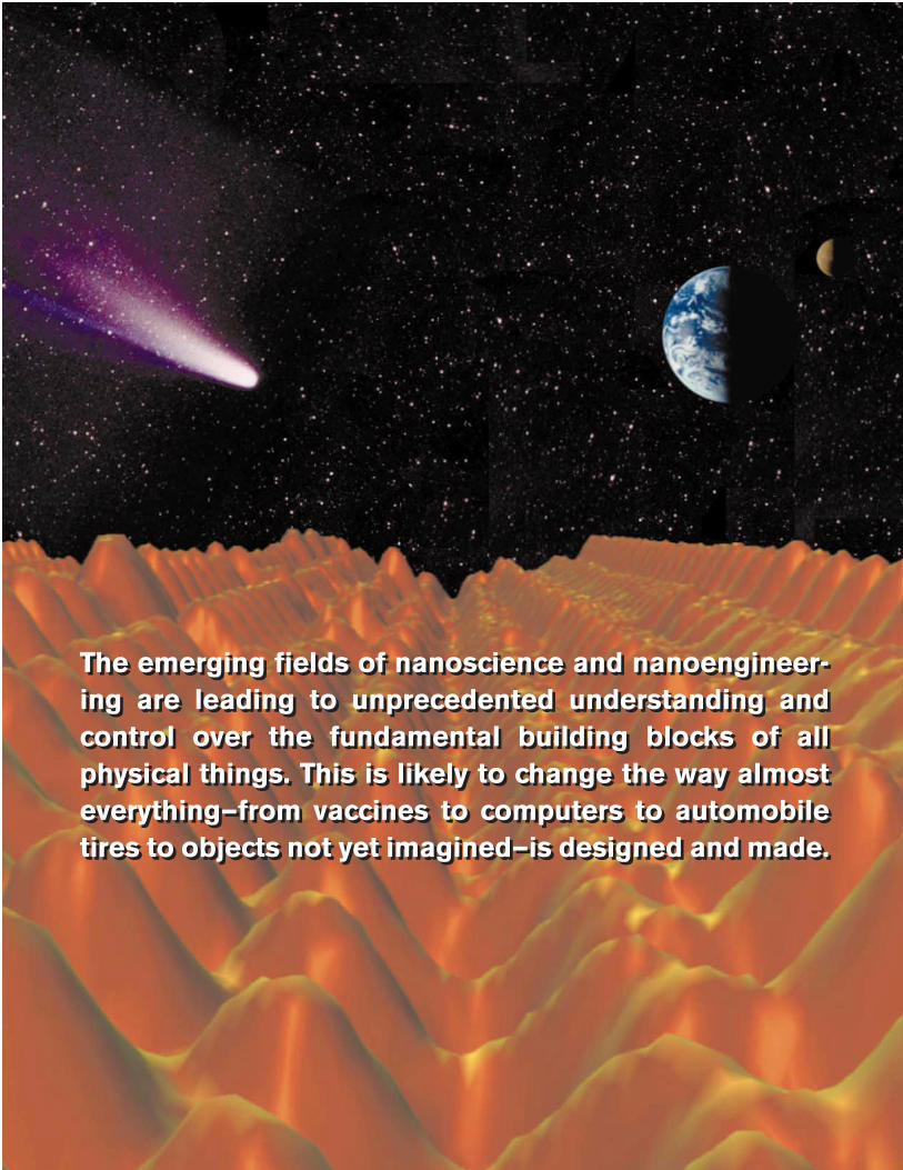
The emerging fields of nanoscience and nanoengineer-ing are leading to unprecedented understanding andcontrol over the fundamental building blocks of allphysical things. This is likely to change the way almosteverything—from vaccines to computers to automobiletires to objects not yet imagined—is designed and made.
The emerging fields of nanoscience and nanoengineer-ing are leading to unprecedented understanding andcontrol over the fundamental building blocks of allphysical things. This is likely to change the way almosteverything—from vaccines to computers to automobiletires to objects not yet imagined—is designed and made.