Embed Size (px)
Citation preview
158 IEEE TRANSACTIONS ON SEMICONDUCTOR MANUFACTURING, VOL. 9, NO. 2, MAY 1996
nchmarking Semiconductor Manufacturing Robert C. Leach” and David A. Hodges, Fellow, ZEEE
Abstract- We are studying the manufacturing performance of semiconductor wafer fabrication plants in the US, Asia, and Europe. There are great similarities in production equipment, manufacturing processes, and products produced at these plants. Nevertheless, data reported here show that important quantita- tive measures of productivity vary by factors of 3 to as much as 5 across an international sample of 16 plants.
We conducted on-site interviews with manufacturing personnel to better understand reasons for the observed wide variations in productivity. We have identified factors in the areas of infor- mation systems, organizational practices, process and technology improvements, and production control that correlate strongly with productivity.
I. INTRODUCTION
HE Competitive Semiconductor Manufacturing (CSM) T Program at the University of California, Berkeley, since April 1991, has been conducting a detailed study of quality, productivity, and competitiveness in semiconductor manufac- turing worldwide. The program is a joint activity of the College of Engineering, the Haas School of Business, and the Berkeley Roundtable on the International Economy at Berkeley, under sponsorship of the Alfred P. Sloan Foundation, and with the cooperation of semiconductor producers from Asia, Europe and the United States. The authors of tbls paper are the project’s CO-Directors. Other contributors are named in the Acknowledgments. This article is based on data and analysis drawn from the continuing program [l].
The CSM program is being conducted by faculty, graduate students and research staff from UC Berkeley’s schools of En- gineering and Business, and Department of Economics. Many of the participating firms are represented on the program’s Industry Advisory Board. The Board played an important role in defining the research agenda. A pilot study was conducted in 1991 with the cooperation of three semiconductor plants. The research plan and survey documents were thereby refined. The main phase of the CSM benchmarking study began in mid-1992 and will continue at least through 1997.
11. FOCUS OF THIS STUDY
Our study focuses on semiconductor wafer processing as needed to produce VLSI chips including memories, micro- processors, signal processors, other logic, and mixed-signal products. Wafer processing takes place in manufacturing plants known as “fabs”. Modern fabs require capital investment in
Manuscript received March 3, 1995; revised December 9, 1995. This work was supported by a grant from the Alfred P. Sloan Foundation, New York, as a part of the Foundation’s program of Manufacturing Industry Studies.
The authors are with the College of Engineering and the Engineering Systems Research Center, University of Califomia, Berkeley, CA 94720 USA.
Publisher Item Identifier S 0894-6507(96)03273-3.
plant and equipment of $500M to $lB each. They are the most costly manufacturing plants found in any industry today. The knowledge and skills required for efficient wafer fabrication require further large, ongoing investments. Manufacturing process sequences are exceedingly complex, with 400 or more sequential operations on a wafer over a span of 20 to 60 24-h days. A gross failure at any step can render a wafer worthless. The salable fraction of the total number of chips on a finished wafer, known as the “chip yield,” varies from zero to loo%, depending on the effectiveness of quality control in avoiding localized defects on chips.
Today’s principal VLSI products including memories, mi- croprocessors, digital signal processors, application-specific logic, etc. are manufactured worldwide using very similar manufacturing equipment and processes. In many cases, 5 to 15 firms world-wide compete in selling interchangeable final products to hundreds of customers. Economic success in wafer fabrication clearly requires maximizing the output of salable products from a large fixed investment. Despite these obvious facts, there is an amazingly large variation in the manufacturing performance of semiconductor firms. The present study is intended to quantify and benchmark manufacturing performance and to identify superior practices in manufacturing technology, factory operation, organization, and management.
Our study has addressed only the wafer fabrication element of the total semiconductor manufacturing cycle. This is the most complex and capital-intensive element. The technologies and processes of packaging semiconductor chips are, how- ever, growing in significance. Semiconductor packaging is the subject of a forthcoming report from another group [2].
m. SOURCES OF DATA AND LIMITATIONS ON ITS DISCLOSURE
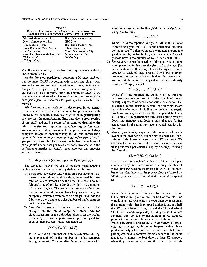
The data and analysis summarized in this report derive from measurements of manufacturing performance and investigation of underlying determinants of performance at 16 wafer fabrica- tion facilities in the United States, Europe, Japan and Taiwan. The companies operating these manufacturing facilities are listed in Table I. In selecting participants, we sought access to plants representing a cross-section of the industry, both internationally and in terms of business models and product mix. We asked for access to plants that had been in operation for at least three years. Substantial effort is required on the part of each participant. Some of those approached declined to participate. Participants who operate several semiconductor manufacturing lines generally opened one of their best lines to this study. Firms participate based on written agreement that we mask the relationship between individual firms and plants. We report results only in anonymous or aggregated forms.
0894-6507/96$05.00 0 1996 IEEE
LEACHMAN AND HODGES: BENCHMARKING SEMICONDUCTOR MANUFACTURING 159
TABLE I COMPANIES PARTICIPATING IN THE MAIN PHASE OF THE C O M P E ~ V E
SEMICONDUCTOR MANUFACTURING SURVEY (FIRST 18 MONTHS)
Advanced Micro Devices, Inc. Cypress Semiconductor, Inc. NEC Corp. Delco Electronics, Inc. Digital Equipment Corp. (2 sites) Intel Corporation Taiwan Semiconductor Mfg. Intemational Business Machines, Inc. ITT Intermetall Toshiba Corp. LSI Logic. Corp
Nihon Semiconductor, Inc.
Oki Electric Industry, Ltd. Silicon Systems, Inc.
Texas Instruments, Inc.
The Berkeley team signs nondisclosure agreements with all participating firms.
As the first step, participants complete a 70-page mail-out questionnaire (MOQ), reporting data concerning clean room size and class, staffing levels, equipment counts, wafer starts, die yields, line yields, cycle times, manufacturing systems, etc. over the last four years. From the completed MOQ’s, we calculate technical metrics of manufacturing performance for each participant. We then rank the participants for each of the metrics.
We observed a great variation in the scores. In an attempt to understand the factors that account for performance dif- ferences, we conduct a two-day visit at each participating site. We tour the manufacturing line, interview a cross-section of the staff, and hold a series of sessions to determine the fab’s strategies for improving manufacturing performance. We assess each fab’s resources for improvement including computer integrated manufacturing (CIM) and information systems, human resources development, deployment of work groups and teams, etc. These more qualitative evaluations of participants’ operational practices are then correlated with the performance metrics to identify those practices that underlie top performance.
Iv. METRICS OF MANUFACTURING PERFORMANCE
The technical metrics we use to measure manufacturing
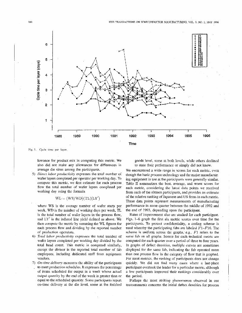
1) Cycle time per wafer layer measures the duration, ex- pressed in fractional working days, consumed by pro- duction lots of wafers from the time of release into the fab until time of exit from the fab, divided by the number of masking layers. The participants report cycle times for each of several process flows they may operate; we compute a weighted average cycle time per layer for the fab, where the weights are the number of wafer starts in each process flow.
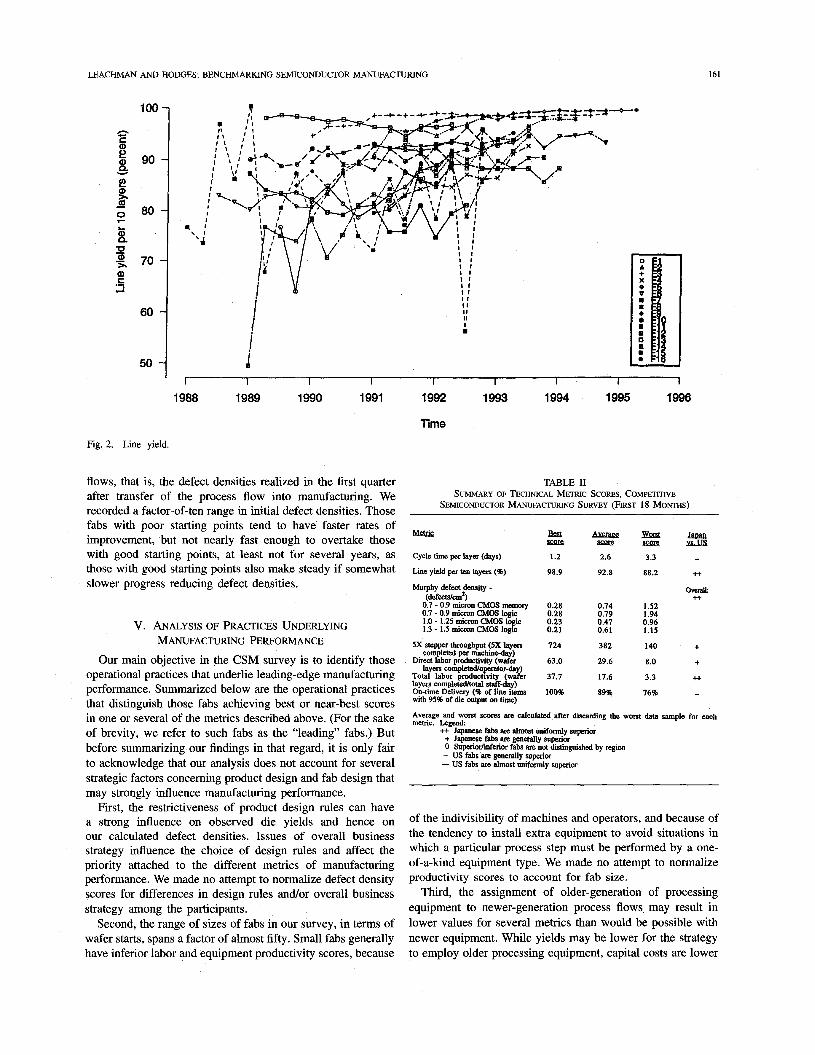
2) Line yield measures the fraction of wafers started that emerge from the fab as completed wafers ready for electrical testing of the individual circuits on the wafer. In monthly periods, the participants report line yield for each of their process flows, calculated as
performance of the participants are defined as follows:
where WO is the number of wafers completed during the month and SC is the number of wafers scrapped during the month. We normalize the reported line yields
into scores expressing the line yield per ten wafer layers using the formula
Lyle = L y ( l O / M L )
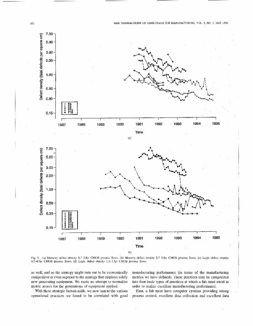
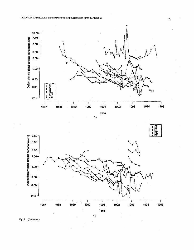
where LY is the reported line yield, ML is the number of masking layers, and LY 10 is the calculated line yield per ten layers. We then compute a weighted average line yield per ten layers for the fab, where the weight for each process flow is the number of wafer starts of the flow. Die yield expresses the fraction of the total whole die on a completed wafer that pass the electrical probe test. The participants report their die yields for the highest volume product in each of their process flows. For memory products, the reported die yield is that after laser repair. We convert the reported die yield into a defect density using the Murphy model
Y = ((1 - e -AD) /AD}2 where Y is the reported die yield, A is the die area in square centimeters, and D is the calculated defect density, expressed as defects per square centimeter. The calculated defect densities account for all yield losses remaining after repair, including spot defects, parametric problems, and any other losses. We compare defect den- sity scores of the participants only after sorting process flows into memory and logic groups that are further categorized by the minimum geometry achievable with the flow. Stepper productivity expresses the number of wafer layers completed per 5X stepper per calendar day (con- sidering only layers exposed using 5X steppers). We estimate the number of wafer operations in a process flow performed per calendar day by 5X steppers using the formula
SL = (WS/7)(NL)(LY’)
where SL is the calculated number of 5X stepper oper- ations per day, WS is the reported average number of wafer starts per week in the process flow, NL is the num- ber of masking layers in the process flow performed on 5X steppers, and LY’ is an inflated line yield computed as
LY’ = (1.0 + LY)/2
where LY is the reported line yield for the process flow. (This inflated line yield allows for half of the total line yield loss to load 5X steppers, or equivalently, it assumes the average wafer that is scrapped makes it through half the 5X layers before being discarded.) The calculated 5X stepper operations per day for all process flows are summed, then divided by the number of 5X steppers present in the fab to obtain the value of the metric. While participants processing a wide variety of prod- ucts must change reticles more frequently than those producing only a few products, we observed that some participants have automated reticle changes to the point that there is almost no lost time on their 5X steppers when they change reticles. We therefore make no al-
IEEE TRANSACTIONS ON SEMICONDUCTOR MANUFACTURING, VOL. 9, NO. 2, MAY 1996
I I I 1 I I I I 1 1988 1989 I990 1991 1992 1993 1994 1995 1996
Time Fig. 1. Cycle time per layer.
lowance for product mix in computing this metric. We also did not make any allowances for differences in average die sizes among the participants.
5 ) Direct labor productivity expresses the total number of wafer layers completed per operator per working day. To compute this metric, we first estimate for each process flow the total number of wafer layers completed per working day using the formula
WL = (WS/WD)(TL)(LY’)
where WS is the average number of wafer starts per week, WD is the number of working days per week, TL. is the total number of wafer layers in the process flow, and LY’ is the inflated line yield defined as above. We then compute the metric by summing the WL figures for each process flow and dividing by the reported number of production operators.
6) Total labor productivity expresses the total number of wafer layers completed per working day divided by the total head count. This metric is computed similarly, except the divisor is the reported total number of fab employees, including dedicated staff from equipment vendors.
7 ) On-time delivery measures the ability of the participants to meet production schedules. It expresses the percentage of items scheduled for output in a week whose actual output quantity by the end of the week is greater than or equal to the scheduled quantity. Some participants report on-time delivery at the die level, some at the finished
goods level, some at both levels, while others declined to state their performance or simply did not know.
We encountered a wide range in scores for each metric, even though the basic process technology and the major manufactur- ing equipment in use at the participants were generally similar. Table I1 summarizes the best, average, and worst scores for each metric, considering the latest data points we received from each of the sixteen participants, and provides an estimate of the relative ranking of Japanese and US firms in each metric. These data points represent measurements of manufacturing performance in some quarter between the middle of 1992 and the end of 1993, depending upon the participant.
Rates of improvement also are studied for each participant. Figs. 1-6 graph the first six metric scores over time for the participants. To protect confidentiality, a coding scheme is used whereby the participating fabs are labeled F1-F16. The scheme is uniform across the graphs, e.g., F1 refers to the same fab on all graphs. Scores for each technical metric are computed for each quarter over a period of three to four years. In graphs of defect densities, multiple curves are sometimes displayed for the same fab, indicating the fab operated more than one process flow in the category of flow that is graphed. For most metrics, the ranking of participants does not change quickly. We did not find many cases where a last-place participant overtook the leader for a particular metric, although a few participants improved their rankings considerably over the period.
Perhaps the most striking phenomenon observed in our measurements concerns the initial defect densities for process
LEACHMAN AND HODGES: BENCHMARKING SEMICONDUCTOR MANUFACTURING 161
100
60
50
. L f
I t 1 1 I t I I I t I 1
\ I
‘4
i I I I t
i II . I
I 1
1988 1989 1990 1991 1992 1993 1994 1995 1996
Time
Fig. 2. Line yield.
flows, that is, the defect densities realized in the first quarter after transfer of the process flow into manufacturing. We recorded a factor-of-ten range in initial defect densities. Those fabs with poor starting points tend to have faster rates of improvement, but not nearly fast enough to overtake those with good starting points, at least not for several years, as those with good starting points also make steady if somewhat slower progress reducing defect densities.
v. ANALYSIS OF PRACTICES UNDERLYING MANUFACTURING PERFORMANCE
Our main objective in the CSM survey is to identify those operational practices that underlie leading-edge manufacturing performance. Summarized below are the operational practices that distinguish those fabs achieving best or near-best scores in one or several of the metrics described above. (For the sake of brevity, we refer to such fabs as the “leading” fabs.) But before summarizing our findings in that regard, it is only fair to acknowledge that our analysis does not account for several strategic factors concerning product design and fab design that may strongly influence manufacturing performance.
First, the restrictiveness of product design rules can have a strong influence on observed die yields and hence on our calculated defect densities. Issues of overall business strategy influence the choice of design rules and affect the priority attached to the different metrics of manufacturing performance. We made no attempt to normalize defect density scores for differences in design rules and/or overall business strategy among the participants.
Second, the range of sizes of fabs in our survey, in terms of wafer starts, spans a factor of almost fifty. Small fabs generally have inferior labor and equipment productivity scores, because
TABLE I1 SUMMARY OF TECHNICAL METRIC SCORES, COMPETITIVE
SEMICONDUCTOR MANUFACTURING SURVEY (FIRST 18 MONTHS)
Cycle time per layer (days)
Line yield per ten layers (%)
Murphy defect density. (defecWc“) 0.7 - 0.9 micron CMOS mmory 0.7 - 0.9 micron CMOS logic 1.0 - 1.25 micron CMOS logic 1.3 - 1 .5 micron CMOS logic
5X stepper throughput (5X layers completed per machineda )
Diwt labor productivity ( w d r layers completed/opemtorday)
Total labor productivity (wafer layers completeahotal staff4ay) On-time Delivery (% of b e items with 95% of die output on time)
1.2 2.6
98.9 92.8
0.28 0.74 0.28 0.79 0.23 0.47 0.21 0.61
724 382
63.0 29.6
37.7 17.6
100% 89%
3.3 - 88.2 *
O d l : ++ 1.52 1.94 0.96 1.15
I40 + 8.0 + 3.3 * 76% -
Average and worst scores are calculated after discarding the worst data sample for each metric. Legend
++ Japanese fabs are almost unifonnly superior + Japanese fabs are genetally superior 0 Superiorhferior fabs are not distinguished by region - US fabs are geuerally superior - US fabs are almost uniformly superior
of the indivisibility of machines and operators, and because of the tendency to install extra equipment to avoid situations in which a particular process step must be performed by a one- of-a-kind equipment type. We made no attempt to normalize productivity scores to account for fab size.
Third, the assignment of older-generation of processing equipment to newer-generation process flows may result in lower values for several metrics than would be possible with newer equipment. While yields may be lower for the strategy to employ older processing equipment, capital costs are lower
162
- 7.50- !!? 5.00- E -
5: 3.00-
g 2.00- .e
?i - nr gj 1.00-
- 7.50 $ 5.00
$ 3.00
3 CT v)
n
Q 2.00 Q) Q) B .e
IEEE TRANSACTIONS ON SEMICONDUCTOR MANUFACTURING, VOL. 9, NO. 2, MAY 1996
I I I I I I I I I
1987 1988 1989 1990 1991 1992 1993 1994 1995
f 4
1 I I I I 1 I I I
1987 1988 1989 1990 1991 1992 1993 1994 1995
Time ~
(b) 1 I
Fig. 3. 0.7-0.9~ CMOS process flows. (d) Logic defect density 1.3-1.5~ CMOS process flows.
(a) Memory defect density 0.7-0.9~ CMOS process flows. (b) Memory defect density 0.7-0.9~ CMOS process flows. (c) Logic defect density
as well, and so the strategy might turn out to be economically competitive or even superior to the strategy that employs solely new processing equipment. We made no attempt to normalize metric scores for the generations of equipment applied.
With these strategic factors aside, we now turn to the various operational practices we found to be correlated with good
manufacturing performance (in terms of the manufacturing metrics we have defined). These practices may be categorized into four basic types of practices at which a fab must excel in order to realize excellent manufacturing performance.
First, a fab must have computer systems providing strong process control, excellent data collection and excellent data
LEACHMAN AND HODGES: BENCHMARKING SEMICONDUCTOR MANUFACTURING 163
1 O.O( E 7.50
22 5.00 3 & 3.00 n 6 2.00 $?
g g 1.00 .@
0
U v)
a, a -
U) c 0.50
8 0.30 c H
0.15
i 987 1988 1989 1990 1991 1992 1993 1994 1995
- 7.50 E !?2 5.00 3 U to
P 3.00
fj 2.00 w- a -U
1 g 1.00 - 2. E -8 0.50 w- 3 P" 0.30
0.15-
9 a '#' \
\ \
I I
I
,*-T,
II
1987 1988 1989 1990 1991 1992 1993 1994 1995
Time
(4 Fig. 3. (Continued.)
164 IEEE TRANSACTIONS ON SEMICONDUCTOR MANUFACTURING, VOL. 9, NO. 2, MAY 1996
8oo 1
L a,
P r 300
200
fn
100 i 0 J
I I I
I 0
lr '
"7
P 7
/
I I I I I 1 I I 1 1988 1989 1990 1991 1992 1993 1994 1995 1996
Time
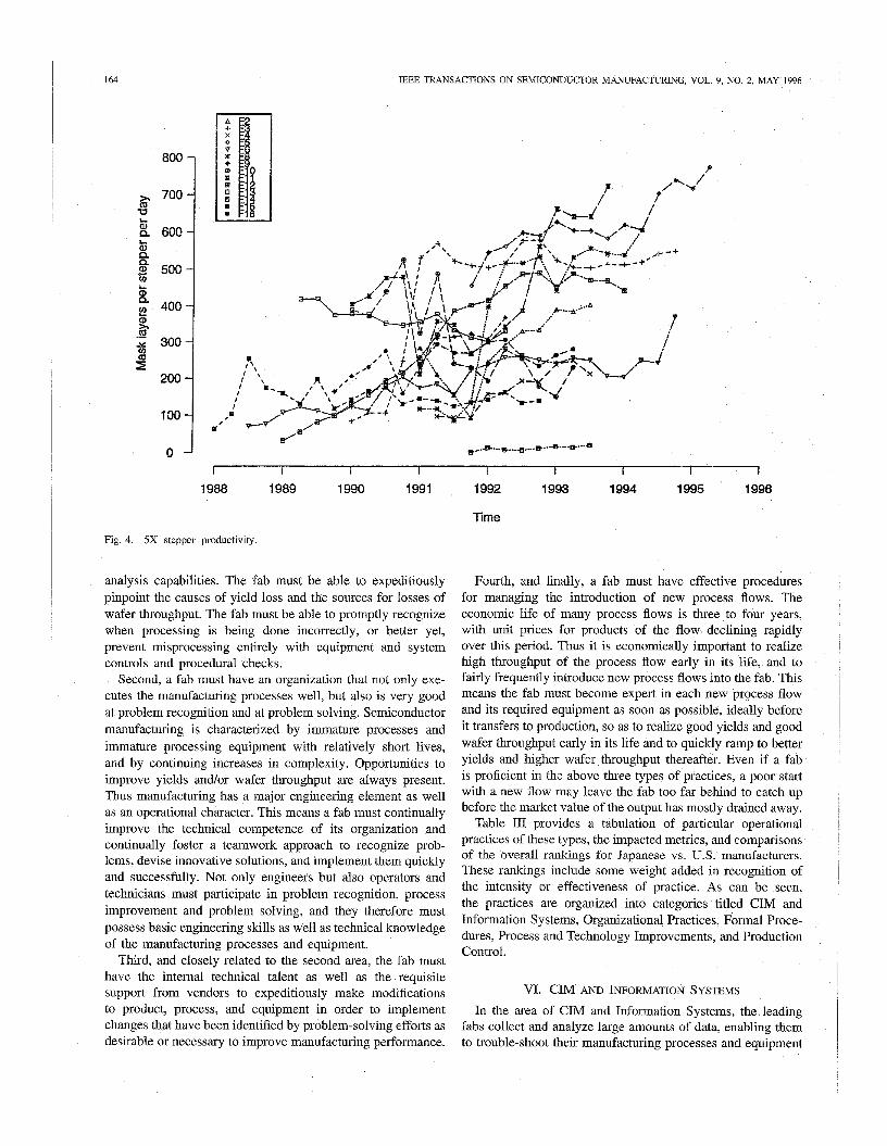
Fig. 4. 5X stepper productivity.
analysis capabilities. The fab must be able to expeditiously pinpoint the causes of yield loss and the sources for losses of wafer throughput. The fab must be able to promptly recognize when processing is being done incorrectly, or better yet, prevent misprocessing entirely with equipment and system controls and procedural checks.
Second, a fab must have an organization that not only exe- cutes the manufacturing processes well, but also is very good at problem recognition and at problem solving. Semiconductor manufacturing is characterized by immature processes and immature processing equipment with relatively short lives, and by continuing increases in complexity. Opportunities to improve yields and/or wafer throughput are always present. Thus manufacturing has a major engineering element as well as an operational character. This means a fab must continually improve the technical competence of its organization and continually foster a teamwork approach to recognize prob- lems, devise innovative solutions, and implement them quickly and successfully. Not only engineers but also operators and technicians must participate in problem recognition, process improvement and problem solving, and they therefore must possess basic engineering skills as well as technical knowledge of the manufacturing processes and equipment.
Third, and closely related to the second area, the fab must have the internal technical talent as well as the requisite support from vendors to expeditiously make modifications to product, process, and equipment in order to implement changes that have been identified by problem-solving efforts as desirable or necessary to improve manufacturing performance.
Fourth, and finally, a fab must have effective procedures for managing the introduction of new process flows. The economic life of many process flows is three to four years, with unit prices for products of the flow declining rapidly over this period. Thus it is economically important to realize high throughput of the process flow early in its life, and to fairly frequently introduce new process flows into the fab. This means the fab must become expert in each new process flow and its required equipment as soon as possible, ideally before it transfers to production, so as to realize good yields and good wafer throughput early in its life and to quickly ramp to better yields and higher wafer throughput thereafter. Even if a fab is proficient in the above three types of practices, a poor start with a new flow may leave the fab too far behind to catch up before the market value of the output has mostly drained away.
Table III provides a tabulation of particular operational practices of these types, the impacted metrics, and comparisons of the overall rankings for Japanese vs. US. manufacturers. These rankings include some weight added in recognition of the intensity or effectiveness of practice. As can be seen, the practices are organized into categories titled CIM and Information Systems, Organizational Practices, Formal Proce- dures, Process and Technology Improvements, and Production Control.
VI. CIM AND INFORMATION SYSTEMS
In the area of CIM and Information Systems, the leading fabs collect and analyze large amounts of data, enabling them to trouble-shoot their manufacturing processes and equipment
LEACHMAN AND HODGES: BENCHMARKING SEMICONDUCTOR MANUFACTI JRING 165
TABLE 111 (CONTINUED) TABLE 111 SUMMARY OF EFFECTIVE MANUFACTURING PRACTICES
F%!xiGs CZM and information systems
SPC
Equipment efficiency
Visual displays of SPC charts,
measurement
equipment tracking, etc.
Automation of data logging
Auto recipe download and/or display
Automated feedback control at photolithography
Yield correlation analysis
In-line electrical measurements
In-line particle measwments
Mevics
Defect Density, Line Yield
quipment throughput, cycle ume, labor productivity
Line yield, defect density, labor productivity, equipment throughput
productivity, equipment throughput
Line yield, cycle time, defect density, labor productivity, equipment throughput
Cycle time, defect density, labor
Defect density
Defect density
Defect density
Defect density
Jauan vs. US
++ ++
+
++
0
0
+t
+ +
Automated trouble messaging Cycle time, line yield, equipment - and automated assistance for trouble-shooting
throughput, labor productivity
TABLE 111 (CONTINUED)
€Bak.G Metrics Influenced , & # n vs. us Formal Procedures
Formal procedures for new Defect density, line yield, ++ process intrvductions equipment throughput
Equipment throughpuf cycle ++ time, line yield, defect density, labm productivity
Organizational Practices
Exchange. of engineers with Defect density, line yield, ++
Integration of engineering groups Defect density ++ Integration of enginwring and Quipment throughput, ++
Opaator and technician Equipment throughput, cycle ++
Mentoring by senior engineers Defect density, line yield, +i
Mentoring by senior operators Line yield, cycle time, ++
Extensive leadership training Defect density, line yield, ++
development fab equipment throughput
manufacturing staff
improvement teams time, lime yield
and supervisors equipment throughput
equipment throughput
equipment throughput
line yield, defect density
“Stretch” goals Defect density, line yield, ++ equipment throughput, labor producuvity
quickly and comprehensively. All participants in our study have embraced statistical process control (SPC) as a means of detecting manufacturing problems and improving process performance. Almost all provide automated notification of out- of-control conditions. The leading fabs rigorously manage their SPC programs, retiring unneeded control charts and adding
hactice Metrics Influenced Japan vs. US
Process and Technology Improvements:
Machine modifications to Line yield, cycle time, labor ++ automate loadlunload or wafer productivity, equipment handling mechanisms throughput
Machine modificatons to duce Defect density, cycle time, ++ particle counts labor productivity, equipment
throughput
yield, equipment throughput Process flow re-design Defect density, cycle time, line +
Product re-design Defect density ++ Machine lights and audio alarms Cycle time, equipment ++
Linked photolithography cells Defect density, cycle time, 0
Automated interbay Cycle time, labor productivity ++
throughput, labor productivity
equipment throughput
lot movement
Production Control
Kanban Cycle time, labor productivity -- Computerized dispatching Cycle time, labor productivity, --
on-time delivery
Production planning based on measured equipment capacity
On-time delivery
Legend: ++ Japanese fabs are almost uniformly more effective + Japanese fabs are generally more effective 0 The most effective practitioners are not distinguished by region - United States fabs are generally more effective - United States fabs are almost uniformly more effective
--
new ones recognized as desirable, adjusting control limits as appropriate, adjusting frequencies of measurements to focus efforts on the most critical areas, and maintaining an effective training program.
SPC measurements are made both of product wafers and of machine conditions, such as particle counts of machine exhaust flows or of blank wafers passed through the machine. The leading fabs have information systems that automatically provide assistance for responding to out-of-control situations, such as auto-display of corrective action guidelines, automatic disabling of equipment or process, automatic notification of the responsible engineers, etc. SPC measurements also are used to trigger preventive maintenance and tool or material replacements.
All of our participants have engineering databases to which they upload some amount of metrology data, SPC measure- ments, and production tracking data (such as which machine was used to process a lot, which operator attended to it, which batch of chemicals was used, etc.). The leading fabs upload more data, and they have automated the upload of much of these data using bar codes or magnetic cards and sensors.
The top fabs efficiently perform end-of-line yield analyzes by integrating their engineering database with the database of die yields and parametric measurements taken at the end of the manufacturing line. Automated statistical correlations are made between die yield results and the data uploaded to the engineering database described above, in order to ascertain what characteristics are common to low-yielding
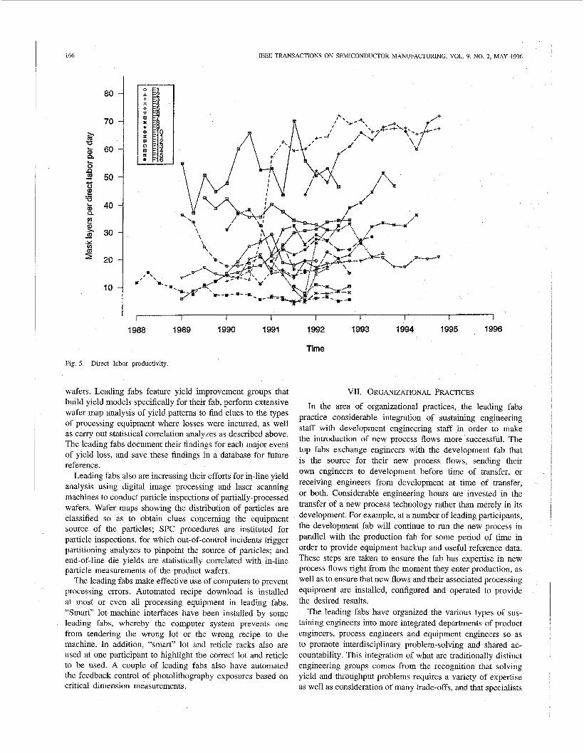
EEE TRANSACTIONS ON SEMICONDUCTOR MANUFACTURING, VOL. 9, NO. 2, MAY 1996
I I I I I I I I 1 1988 1989 1990 1991
Fig. 5. Direct labor productivity
wafers. Leading fabs feature yield improvement groups that build yield models specifically for their fab, perform extensive wafer map analysis of yield patterns to find clues to the types of processing equipment where losses were incurred, as well as carry out statistical correlation analyzes as described above. The leading fabs document their findings for each major event of yield loss, and save these findings in a database for future reference.
Leading fabs also are increasing their efforts for in-line yield analysis using digital image processing and laser scanning machines to conduct particle inspections of partially-processed wafers. Wafer maps showing the distribution of particles are classified so as to obtain clues concerning the equipment source of the particles; SPC procedures are instituted for particle inspections, for which out-of-control incidents trigger partitioning analyzes to pinpoint the source of particles; and end-of-line die yields are statistically correlated with in-line particle measurements of the product wafers.
The leading fabs make effective use of computers to prevent processing errors. Automated recipe download is installed at most or even all processing equipment in leading fabs. “Smart” lot-machine interfaces have been installed by some leading fabs, whereby the computer system prevents one from tendering the wrong lot or the wrong recipe to the machine. In addition, “smart” lot and reticle racks also are used at one participant to highlight the correct lot and reticle to be used. A couple of leading fabs also have automated the feedback control of photolithography exposures based on critical dimension measurements.
1992 1993 1994 1995 1996
Time
VII. ORGANIZATIONAL PRACTICES
In the area of organizational practices, the leading fabs practice considerable integration of sustaining engineering staff with development engineering staff in order to make the introduction of new process flows more successful. The top fabs exchange engineers with the development fab that is the source for their new process flows, sending their own engineers to development before time of transfer, or receiving engineers from development at time of transfer, or both. Considerable engineering hours are invested in the transfer of a new process technology rather than merely in its development. For example, at a number of leading participants, the development fab will continue to run the new process in parallel with the production fab for some period of time in order to provide equipment backup and useful reference data. These steps are taken to ensure the fab has expertise in new process flows right from the moment they enter production, as well as to ensure that new flows and their associated processing equipment are installed, configured and operated to provide the desired results.
The leading fabs have organized the various types of sus- taining engineers into more integrated departments of product engineers, process engineers and equipment engineers so as to promote interdisciplinary problem-solving and shared ac- countability. This integration of what are traditionally distinct engineering groups comes from the recognition that solving yield and throughput problems requires a variety of expertise as well as consideration of many trade-offs, and that specialists
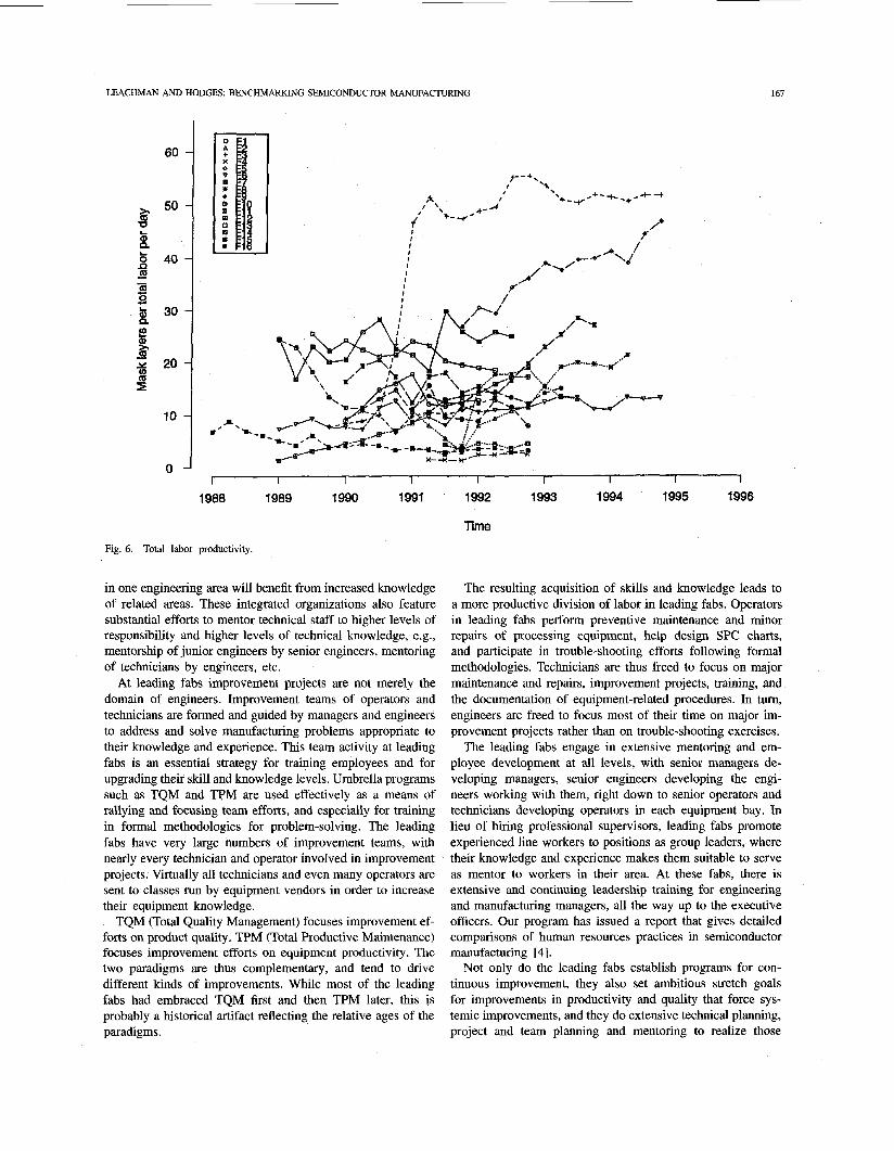
LEACHMAN AND HODGES: BENCHMARKING SEMICONDUCTOR MANUFACTURING
60 -
50 - 3 U
b 4 0 - .o lu lu - - c $2 f 30 - 9.
c P U 20- 3 E
10 -
0 -
167
I I I I I I I I 1 1988 1989 1990 1991 1992 1993 1994 1995 1996
Time
Fig. 6. Total labor productivity.
in one engineering area will benefit from increased knowledge of related areas. These integrated organizations also feature substantial efforts to mentor technical staff to higher levels of responsibility and higher levels of technical knowledge, e.g., mentorship of junior engineers by senior engineers, mentoring of technicians by engineers, etc.
At leading fabs improvement projects are not merely the domain of engineers. Improvement teams of operators and technicians are formed and guided by managers and engineers to address and solve manufacturing problems appropriate to their knowledge and experience. This team activity at leading fabs is an essential strategy for training employees and for upgrading their skill and knowledge levels. Umbrella programs such as TQM and TPM are used effectively as a means of rallying and focusing team efforts, and especially for training in formal methodologies for problem-solving. The leading fabs have very large numbers of improvement teams, with nearly every technician and operator involved in improvement projects. Virtually all technicians and even many operators are sent to classes run by equipment vendors in order to increase their equipment knowledge.
TQM (Totd Quality Management) focuses improvement ef- forts on product quality. TPM (Total Productive Maintenance) focuses improvement efforts on equipment productivity. The two paradigms are thus complementary, and tend to drive different kinds of improvements. While most of the leading fabs had embraced TQM first and then TPM later, this is probably a historical artifact reflecting the relative ages of the paradigms.
The resulting acquisition of skills and knowledge leads to a more productive division of labor in leading fabs. Operators in leading fabs perform preventive maintenance and minor repairs of processing equipment, help design SPC charts, and participate in trouble-shooting efforts following formal methodologies. Technicians are thus freed to focus on major maintenance and repairs, improvement projects, training, and the documentation of equipment-related procedures. In turn, engineers are freed to focus most of their time on major im- provement projects rather than on trouble-shooting exercises.
The leading fabs engage in extensive mentoring and em- ployee development at all levels, with senior managers de- veloping managers, senior engineers developing the engi- neers working with them, right down to senior operators and technicians developing operators in each equipment bay. In lieu of hiring professional supervisors, leading fabs promote experienced line workers to positions as group leaders, where their knowledge and experience makes them suitable to serve as mentor to workers in their area. At these fabs, there is extensive and continuing leadership training for engineering and manufacturing managers, all the way up to the executive officers. Our program has issued a report that gives detailed comparisons of human resources practices in semiconductor manufacturing [4].
Not only do the leading fabs establish programs for con- tinuous improvement, they also set ambitious stretch goals for improvements in productivity and quality that force sys- temic improvements, and they do extensive technical planning, project and team planning and mentoring to realize those
168 IEEE TRANSACTIONS ON SEMICONDUCTOR MANUFACTURING, VOL. 9, NO. 2, MAY 1996
goals. Many of the factors just mentioned closely parallel successful practices of world leaders in automobile assembly, as described in [3].
In the area of formal procedures, the leading fabs have established formal procedures governing the transfer and in- troduction of new process flows. There also are efforts at leading fabs to modularize process design, whereby new pro- cesses make use of proven modules from previous-generation processes, where feasible to do so. Such procedures serve to maximize the likelihood that new processes provide favorable yields in the first quarter of production, and that volume may be ramped quickly.
While all of our participants use SPC as a formal procedure for in-line measurement of quality, and all of our participants make efforts to measure equipment availability and utilization, the leading fabs have formal procedures for the measurement of true equipment productivity rather than merely its utiliza- tion. The leading fabs also have formalized the improvement of procedures for equipment maintenance, operation, analysis and training under the TPM paradigm.
VIII. PROCESS AND EQUIPMENT IMPROVEMENTS
In the area of process and equipment improvements, the leading fabs make useful modifications to processing equip- ment to reduce downtime, to reduce particles, to reduce wafer breakage or scratches, to reduce handling, to reduce machine setups, to reduce the need to process test or pilot wafers, and to reduce unit processing times. They have the necessary expertise on-site, they obtain support from equipment vendors as required, and they have an organizational structure that integrates process and equipment engineers so as to deduce the most prudent equipment modifications to make considering the desired process characteristics. The leading fabs have installed lights and audio alarms on the processing machines to focus attention on idle or malfunctioning machines. Photolithogra- phy at the leading fabs is performed in linked cells achieving superior die yields, low rates of rework, low cycle times and high throughput.
Sometimes, modifying the equipment is not the most effec- tive solution to a yield problem. The leading fabs also make changes to product designs or process flows for increased man- ufacturability. Such changes reflect an organizational structure that integrates product, process and equipment engineers, en- abling them to identify and make trade-offs between potential equipment and product changes.
IX. INTRODUCTION OF NEW PROCESSES AND PRODUCTS
Fig. 3(a)-(d) make it clear that manufacturing defect density at the time first production product is shipped to customers varies by a factor of 5 to 10 among the fabs studied. While learning rates for defect density vary somewhat, rarely is a bad start overcome by subsequent rapid improvement. This obser- vation underlines the critical importance of highly disciplined development activity, and of tight coupling between develop- ment and manufacturing when the transfer takes place. The best performers accomplish successful new process introduc- tions with temporary or permanent transfers of key personnel.
Special mention should be made of the application of stan- dafd mechanical interface (SMIF) technology, involving the implementation of portable micro-environments for processing equipment and lots [5]. We saw one participant, using an older and much more modest clean room than other participants operating comparable process flows, obtain world-class die yields. The introduction of SMIF technology clearly extended the economic life of this older fab and thus constitutes a very good technological improvement. The isolation of each machine from the rest of the fab also facilitated staged and selective upgrading of the equipment set in the fab.
Special mention also should be made with respect to the leading fab in terms of cycle time. Over several years, this fab has steadily rearranged its layout to break up the stan- dard farm-type layout in favor of smaller cells of equipment handling a smaller variety of operation sequences. While in the past cell-type layouts have been resisted by many fab designers for fear of lost equipment utilization, this same fab is also our leader in 5X stepper throughput. This fab has demonstrated that a more cell-type layout represents a technological improvement, in that cycle times can be reduced while achieving leading-edge equipment throughput.
Finally, in the area of production control, the leading fabs perform automated production planning based on measured equipment capacity and cycle times to achieve high levels of on-time delivery. Re-planning is performed frequently and swiftly to keep up with revised intelligence on market demand and customer orders. On the factory floor, both Kanban and computer-assisted dispatching (lot sequencing) are used by leading fabs to improve cycle time as well as on-time delivery.
,
I
X. SUMMARY
Japanese plants examined as a part of our semiconductor manufacturing study on the whole are more effective in imple- menting preferred manufacturing practices. Management and workers share a firm commitment to continuing improvements. As a consequence, quality and productivity measures for those plants are excellent and improve steadily. While a few US plants achieve similar excellence, many US plants in our survey fall far behind the leaders in these categories. On the other hand, US plants are generally more effective in terms of cycle time and on-time delivery performance.
Our prescription for improved US manufacturing competi- tiveness calls for the high quality management and leadership frequently exhibited by US firms in research, product defini- tion, finance, and marketing to be matched in manufacturing. While some readers may wonder if there may be social, cultural or legal barriers inhibiting implementation in US plants of leading-edge organizational practices described in this paper, we find nothing particularly “Japanese” about them. Indeed, the US plants achieving excellence similar to our Japanese participants tend to exhibit similar organizational practices.
ACKNOWLEDGMENT Many people contributed to the research summarized in
this paper. Those who authored sections of [l] (in addition
LEACHMAN AND HODGES: BENCHMARKING SEMICONDUCTOR MANUFACTURING 169
to the first author) include D. Bailey, R. Benson, M. Borms, S. Cunningham, N. Hatch, D. Mowery, B. Saeed, T. Sloan, C. Spanos, R. Srikanth, and K. Voros. Others who contributed importantly to the research are N. Berglund, C. Brown, S. Reichelstein, and V. Sohoni.
REFERENCES
[ 11 R. Leachman, Ed., The Competitive Semiconductor Manufacturing Sur- vey: Second Report on Results of the Main Phase, Rep. CSM-08, Eng. Syst. Res. Center, Univ. of California, Berkeley, Sept. 1994. (Report will be sent at no charge in response to email request to [email protected] or FAX to CSM at 510-642-1403.)
[2] M. Kelly et al., Electronic Manufacturing and Packaging in Japan, JTEC Panel Report, Int. Technol. Res. Inst., Loyola College, Baltimore, MD, forthcoming, 1995.
[3] Womak, Jones, and Roos, The Machine that Changed the World, Rawson Associates, 1990.
[4] C. Brown, Ed., The Competitive Semiconductor Manufacturing Human Resources Project, Rep. CSM-09, Eng. Syst. Res. Center, Univ. of California, Berkeley, Sept. 1994. (Report will be sent at no charge in response to email request to [email protected] or FAX to CSM at 510-642-1403.)
[SI M. Parikh and U. Kaempf, “SMIF: A technology for wafer cassette transfer in VLSI manufacturing,” Solid State Technol., vol. 27, no. 7, p. 111, July 1984.
Robert C. Leachman received the A.B. degee in physics and mathematics, and the M.S. and Ph.D. degrees in operations research, from the University of California, Berkeley.
He has been with the University of California, Berkeley since 1979 as CO-Director of the Com- petitive Semiconductor Manufacturing Program and Professor of Industrial Engineering and Operations Research. Since 1984 he has led Berkeley research efforts in production planning, scheduling and effi- ciency analysis of semiconductor manufacturing. In
particular, he is the author of the Berkeley Planning System (BPS), a software for automating company-wide production planning and delivery quotation in semiconductor manufacturing now in use at several large semiconductor firms.
Dr. Leachman was a recipient of the Franz Edelman Award for outstand- ing practice of the management sciences from the Institute for Operations Research and the Management Sciences (INFORMS).
David A. Hodges (S’59-M65-SM’7l-F‘77) re- ceived the B.E.E. degree from Cornell University, Ithaca, NY, and the M.S. and Ph.D. degrees from the University of California, Berkeley.
From 1966 to 1970, he worked at Bell Tele- phone Laboratories, first at Murray Hill, NJ, then as Head of the System Elements Research Department, Holmdel, NJ. He is now Professor of Electrical Engineering and Computer Sciences at the Univer- sity of California, Berkeley, where he has been a member of the faculty since 1970. Following service
as Chairman of the EECS Department, he became Dean of the College of Engineering on July 1, 1990. Since 1970 Professor Hodges has been active in teaching and research on microelectronics technology and design. Since 1984 his research has centered on semiconductor manufacturing systems.
Dr. Hodges was the founding Editor of the IEEE TRANSACTIONS ON SEMICONDUCTOR MANUFACTURING, a past Editor of the IEEE JOURNAL OF SOLID-STATE CIRCUITS, and a past Chairman of the Intemational Solid-state Circuits Conference. With R. W. Brodersen and P. R. Gray, he received the 1983 IEEE Moms N. Liebmann Award for pioneering work on switched- capacitor circuits. He is a Fellow of the AAAS, and a Member of the National Academy of Engineering.