Embed Size (px)
Citation preview

© Semiconductor Components Industries, LLC, 2016
July, 2016 − Rev. P01 Publication Order Number:
NCP1240G/D
NCP1240G
Product Preview
Fixed Frequency CurrentMode Controller for FlybackConverters
The NCP1240G is a new fixed−frequency current−mode controllerfeaturing the Dynamic Self−Supply. This function greatly simplifiesthe design of the auxiliary supply and the VCC capacitor by activatingthe internal startup current source to supply the controller duringstart−up, transients, latch, stand−by etc. This device contains a specialHV detector which detect the application unplug from the AC inputline and triggers the X2 discharge current. This HV structure allowsthe brown−out detection as well.
It features a timer−based fault detection that ensures the detection ofoverload and an adjustable compensation to help keep the maximumpower independent of the input voltage.
Due to frequency foldback, the controller exhibits excellentefficiency in light load condition while still achieving very lowstandby power consumption. Internal frequency jittering, rampcompensation, and a versatile latch input make this controller anexcellent candidate for the robust power supply designs.
A dedicated Off mode allows to reach the extremely low no loadinput power consumption via “sleeping” whole device and thusminimize the power consumption of the control circuitry.
Features• Fixed−Frequency Current−Mode Operation (65 kHz and 100 kHz
frequency options)• Frequency Foldback then Skip Mode for Maximized Performance in
Light Load and Standby Conditions• Timer−Based Overload Protection with Latched (Option G)
• High−voltage Current Source with Brown−Out Detection andDynamic Self−Supply, Simplifying the Design of the VCC Circuitry
• Frequency Modulation for Softened EMI Signature
• Adjustable Overpower Protection Dependant on the Bulk Voltage
• Latch−off Input Combined with the Overpower Protection SensingInput
• VCC Operation up to 28 V, With Overvoltage Detection
• 500/800 mA Source/Sink Drive Peak CurrentCapability
• 10 ms Soft−Start
• Internal Thermal Shutdown
• No−Load Standby Power < 30 mW
• X2 Capacitor in EMI Filter Discharging Feature
• These Devices are Pb−Free and Halogen Free/BFR Free
Typical Applications• AC−DC Adapters for Notebooks, LCD, and Printers
• Offline Battery Chargers
• Consumer Electronic Power Supplies
• Auxiliary/Housekeeping Power Supplies
• Offline Adapters for Notebooks
This document contains information on a product under development. ON Semiconductorreserves the right to change or discontinue this product without notice.
SOIC−7CASE 751U
MARKINGDIAGRAM
www.onsemi.com
40G065ALYWX
�1
8
40G065 = Specific Device CodeA = Assembly LocationL = Wafer LotY = YearW = Work Week� = Pb−Free Package
See detailed ordering and shipping information on page 43 ofthis data sheet.
ORDERING INFORMATION
1 8
5
3
4
(Top View)
Latch
CS
HV
PIN CONNECTIONS
6
2FB
GND DRV
VCC
NCP1240G
www.onsemi.com2
TYPICAL APPLICATION EXAMPLE
Figure 1. Flyback Converter Application Using the NCP1240G
GND
GND
GND
GND
NCP1240GND
GND
PC817
GND
GND
GND
GND
NCP431
GND GND
GND
L2 L1
Q1
D2 D1
COUT
RS
EN
SE
RC
LAM
P
CC
LAM
P
RLO
AD
CB
ULK
D7
D6
D5
D4
LATCH1
FB2
CS3
GND4 DRV 5VCC 6
HV 8IC1
TR
2
1
4
3
6
5D3
C1
ROPP
D8
NTC
OK11
23
4
C2
R1
R2
R4
R3
IC2
C3
D9
D10
RHV
CX1CX2
12
34
12
34
C4
+
+
W1
W2
W3
ac input
dc output
OPTIONS
Part Option Frequency OCP Fault
NCP1240 G 65 kHz Latched
PIN FUNCTION DESCRIPTION
Pin No Pin Name Function Pin Description
1 LATCH Latch−Off Input Pull the pin up or down to latch−off the controller. An internal current sourceallows the direct connection of an NTC for over temperature detection.
2 FB Feedback + Shutdown pin An optocoupler collector to ground controls the output regulation. The partgoes to the low consumption Off mode if the FB input pin is pulled to GND.
3 CS Current Sense This Input senses the Primary Current for current−mode operation, andoffers an overpower compensation adjustment.
4 GND − The controller ground
5 DRV Drive output Drives external MOSFET
6 VCC VCC input This supply pin accepts up to 28 Vdc, with overvoltage detection. The pin isconnected to an external auxiliary voltage. It is not allowed to connectanother circuit to this pin to keep low input power consumption.
8 HV High−voltage pin Connects to the rectified AC line to perform the functions of Start−upCurrent Source, Self−Supply, brown−out detection and X2 capacitordischarge function and the HV sensing for the overpower protectionpurposes. It is not allowed to connect this pin to DC voltage.

NCP1240G
www.onsemi.com3
SIMPLIFIED INTERNAL BLOCK SCHEMATIC
Figure 2. Simplified Internal Block Schematic
freq folback
jittering
Vsk
ip
Skip_CMP
SkipB
Vra
mp_
offs
et
1.4V
4uMho
Ramp_OTACSref
Div
isio
n ra
tio 4
Inte
rnal
res
itanc
e 40
k
Soft Start timer
Reset
QSet
Qb
Clamp
FB
CS
DRV
GND
VCC
Rfb
1
Rfb
2R
fb3
Fau
ltB
Latc
hB
PWM_CMP
Vfb(reg)
MAX_ton
Bro
wn_
Out
B
PWM
V to I
Iopc = 0.5u*(Vhv−125)
Vfb
(opc
)
Von
Off_mode_CMP1
ICstart
FBbuffer
Vhv
DC
sam
ple
2.2V
VCC
UVLO_CMP
Vcc
OF
F
9.3V
LATCH VccOVP
OTP
Vot
p
0.4V
Vov
p
2.5V
OTP_CMP
OVP_CMP
Vcl
amp
1.2V
Rcl
amp
1k
HV
Brown_Out
VccOVP_CMP
Vcc
OV
P
26V
Intc
Vdd
Intc
SS
_end
Set Q
Reset Qb
Latch
Brown_Out
RESET
OVPAC_Off
UVLO
VCC
5uA
Vcc_Int
IC stopB
Vhv DC sample
SG & X2 & Vcc
Vdd reg
Vdd
Vcc regulator
PowerOnReset_CMP
Vcc
(reg
)V
ccR
ES
ET
10.8
V5V
control
8 m
A
current source
ICst
artB
TSD
RESETON_CMP
STOP_CMP
Vcc
ON
Vcc
MIN
12V
8.4V
VccON
VccMIN
GoToOffMode timer 500ms
Set Q
Reset Qb
0.8V
Vof
f
Off_mode_CMP2
FM input
OSC 65kHz
PFM input
Square output
Saw output
ton_max output
3.0V
Vdd
1uA
Fault timer
TSD
Latc
h m
anag
emen
t
FaultIlimit_CMP
Vili
m
0.7V
LEB 120nsCSstop_CMP
VC
Sst
op
1.05
V
TSD
Latch
RESETIlimit
MAX_ton
Autorecovery timer
Brown_Out
Reset
QSet
Qb
IC stop
Transient timer up/downFault
Itran_CMP
Vcs
(tra
n)0.
5V
Itran
4 events timer
Reset
QSet
Qb
50 usFilter
350 usFilter
10 usFilter
Dual HVStart−up
SoftStart_CMP
Enable
SS_end

NCP1240G
www.onsemi.com4
MAXIMUM RATINGS
Rating Symbol Value Unit
DRV(pin 5)
Maximum voltage on DRV pin(Dc−Current self−limited if operated within the allowed range) (Note 1)
–0.3 to 20±1000 (peak)
VmA
VCC(pin 6)
VCCPower Supply voltage, VCC pin, continuous voltagePower Supply voltage, VCC pin, continuous voltage (Note 1)
–0.3 to 28±30 (peak)
VmA
HV(pin 8)
Maximum voltage on HV pin(Dc−Current self−limited if operated within the allowed range)
–0.3 to 500±20
VmA
Vmax Maximum voltage on low power pins (except pin 5, pin 6 and pin 8)(Dc−Current self−limited if operated within the allowed range) (Note 1)
–0.3 to 10±10 (peak)
VmA
R�J−A Thermal Resistance SOIC−7Junction-to-Air, low conductivity PCB (Note 2)Junction-to-Air, medium conductivity PCB (Note 3)Junction-to-Air, high conductivity PCB (Note 4)
162147115
°C/W
R�J−C Thermal Resistance Junction−to−Case 73 °C/W
TJMAX Operating Junction Temperature −40 to +150 °C
TSTRGMAX Storage Temperature Range −60 to +150 °C
ESD Capability, HBM model (All pins except HV) per JEDEC Standard JESD22,Method A114E
> 2000 V
ESD Capability, Machine Model per JEDEC Standard JESD22, Method A115A > 200 V
Stresses exceeding those listed in the Maximum Ratings table may damage the device. If any of these limits are exceeded, device functionalityshould not be assumed, damage may occur and reliability may be affected.1. This device contains latch-up protection and exceeds 100 mA per JEDEC Standard JESD78.2. As mounted on a 80 x 100 x 1.5 mm FR4 substrate with a single layer of 50 mm2 of 2 oz copper traces and heat spreading area. As specified
for a JEDEC 51-1 conductivity test PCB. Test conditions were under natural convection or zero air flow.3. As mounted on a 80 x 100 x 1.5 mm FR4 substrate with a single layer of 100 mm2 of 2 oz copper traces and heat spreading area. As specified
for a JEDEC 51-2 conductivity test PCB. Test conditions were under natural convection or zero air flow.4. As mounted on a 80 x 100 x 1.5 mm FR4 substrate with a single layer of 650 mm2 of 2 oz copper traces and heat spreading area. As specified
for a JEDEC 51-3 conductivity test PCB. Test conditions were under natural convection or zero air flow.
ELECTRICAL CHARACTERISTICS (For typical values TJ = 25°C, for min/max values TJ = −40°C to +125°C, VHV = 125 V, VCC = 11 V unless otherwise noted)
Characteristics Test Condition Symbol Min Typ Max Unit
HIGH VOLTAGE CURRENT SOURCE
Minimum Voltage for Current SourceOperation
VHV(min) − 30 40 V
Current Flowing Out of VCC Pin(X2 discharge current value is equal to Istart2)
VCC = 0 VVCC = VCC(on) − 0.5 V
Istart1Istart2
0.25
0.58
0.811
mA
Off−state Leakage Current VHV = 500 V, VCC = 15 V Istart(off) 10 25 50 �A
Off−mode HV Supply Current VHV = 141 V,VHV = 325 V,
VCC loaded by 4.7 �F cap
IHV(off) −−
4550
6070
�A
SUPPLY
HV Current Source Regulation Threshold VCC(reg) 8 11 − V
Turn−on Threshold Level, VCC Going UpHV Current Source Stop Threshold
VCC(on) 11.0 12.0 13.0 V
HV Current Source Restart Threshold VCC(min) 7.8 8.4 9.0 V
Turn−off Threshold (Note 5) VCC(off) 8.8 9.3 9.8 V
Overvoltage Threshold VCC(ovp) 25 26.5 28 V
5. VCC(off) < VCC(min) with the minimum gap 0.5 V.6. Internal supply current only, currents sourced via FB pin is not included (current is flowing in GND pin only).7. Guaranteed by design.8. CS pin source current is a sum of Ibias and IOPC, thus at VHV = 125 V is observed the Ibias only, because IOPC is switched off.
NCP1240G
www.onsemi.com5
ELECTRICAL CHARACTERISTICS (For typical values TJ = 25°C, for min/max values TJ = −40°C to +125°C, VHV = 125 V, VCC = 11 V unless otherwise noted)
Characteristics UnitMaxTypMinSymbolTest Condition
SUPPLY
Blanking Duration on VCC(off) and VCC(ovp)Detection
tVCC(blank) − 10 − �s
VCC Decreasing Level at Which the InternalLogic Resets
VCC(reset) 4.8 7.0 7.7 V
VCC Level for ISTART1 to ISTART2 Transition VCC(inhibit) 0.2 0.8 1.25 V
Internal Current Consumption (Note 6) DRV open, VFB = 3 V, 65 kHzDRV open, VFB = 3 V, 100 kHz
Cdrv = 1 nF, VFB = 3 V, 65 kHzCdrv = 1 nF, VFB = 3 V, 100 kHz
Off mode (skip or before start−up)
Fault mode (fault or latch)
ICC1ICC1
ICC2ICC2
ICC3
ICC4
1.31.3
1.82.0
0.5
0.35
1.851.85
2.62.9
0.65
0.5
2.22.2
3.03.2
0.8
0.7
mA
BROWN−OUT
Brown−Out Thresholds VHV going upVHV going down
VHV(start)VHV(stop)
10294
111103
120112
V
Timer Duration for Line Cycle Drop−out tHV 35 50 75 ms
X2 DISCHARGE
Comparator Hysteresis Observed at HV Pin VHV(hyst) 1.5 3.5 5 V
HV Signal Sampling Period Tsample − 1.0 − ms
Timer Duration for No Line Detection tDET 43 64 86 ms
Discharge Timer Duration tDIS 43 64 86 ms
OSCILLATOR
Oscillator Frequency fOSC 5887
65100
72109
kHz
Maximum On Time for TJ = 25°C to +125°COnly
fOSC = 65 kHzfOSC = 100 kHz
tONmax(65kHz)tONmax(100kHz)
11.57.5
12.38.0
13.18.5
�s
Maximum On Time fOSC = 65 kHzfOSC = 100 kHz
tONmax(65kHz)tONmax(100kHz)
11.37.4
12.38.0
13.18.5
�s
Maximum Duty Cycle (corresponding tomaximum on time at maximum switchingfrequency)
fOSC = 65 kHzfOSC = 100 kHz
DMAX − 80 − %
Frequency Jittering Amplitude, in Percentageof FOSC
Ajitter ±3 ±5.5 ±8 %
Frequency Jittering Modulation Frequency Fjitter 85 125 165 Hz
FREQUENCY FOLDBACK
Feedback Voltage Threshold Below WhichFrequency Foldback Starts
TJ = 25°C VFB(foldS) 2.35 2.5 2.6 V
Feedback Voltage Threshold Below WhichFrequency Foldback is Complete
TJ = 25°C VFB(foldE) 1.4 1.5 1.6 V
Minimum Switching Frequency VFB = Vskip(in) + 0.1 fOSC(min) 23 27 32 kHz
OUTPUT DRIVER
Rise Time, 10% to 90% of VCC VCC = VCC(min) + 0.2 V, CDRV = 1 nF
trise − 40 70 ns
5. VCC(off) < VCC(min) with the minimum gap 0.5 V.6. Internal supply current only, currents sourced via FB pin is not included (current is flowing in GND pin only).7. Guaranteed by design.8. CS pin source current is a sum of Ibias and IOPC, thus at VHV = 125 V is observed the Ibias only, because IOPC is switched off.
NCP1240G
www.onsemi.com6
ELECTRICAL CHARACTERISTICS (For typical values TJ = 25°C, for min/max values TJ = −40°C to +125°C, VHV = 125 V, VCC = 11 V unless otherwise noted)
Characteristics UnitMaxTypMinSymbolTest Condition
OUTPUT DRIVER
Fall Time, 90% to 10% of VCC VCC = VCC(min) + 0.2 V, CDRV = 1 nF
tfall − 40 70 ns
Current Capability VCC = VCC(min) + 0.2 V,CDRV = 1 nF
DRV high, VDRV = 0 VDRV low, VDRV = VCC
IDRV(source)IDRV(sink)
−−
500800
−−
mA
Clamping Voltage (maximum gate voltage) VCC = VCCmax – 0.2 V, DRV high,RDRV = 33 k�, Cload = 220 pF
VDRV(clamp) 11 13.5 16 V
High−state Voltage Drop VCC = VCC(min) + 0.2 V, RDRV = 33 k�, DRV high
VDRV(drop) − − 1 V
CURRENT SENSE
Input Pull−up Current VCS = 0.7 V Ibias − 1 − �A
Maximum Internal Current Setpoint VFB > 3.5 V VILIM 0.66 0.70 0.74 V
Propagation Delay from VIlimit Detection toDRV Off
VCS = VILIM tdelay − 80 110 ns
Leading Edge Blanking Duration for VILIM tLEB 200 250 340 ns
Threshold for Fast Fault Protection Activation VCS(stop) 0.95 1.05 1.15 V
Leading Edge Blanking Duration for VCS(stop)(Note 7)
tBCS 90 120 150 ns
Soft−start Duration From 1st pulse to VCS = VILIM tSSTART 8 11 14 ms
INTERNAL SLOPE COMPENSATION
Slope of the Compensation Ramp Scomp(65kHz)Scomp(100kHz)
−−
−32.5−50
−−
mV /�s
FEEDBACK
Internal Pull−up Resistor TJ = 25°C RFB(up) 30 40 50 k�
VFB to Internal Current Setpoint DivisionRatio
KFB − 4 − −
Internal Pull−up Voltage on the FB Pin(Note 7)
VFB(ref) 4.5 5 5.5 V
Feedback Voltage Below which the PeakCurrent is Frozen
TJ = 25°C VFB(off) − 0.8 − V
SKIP CYCLE MODE
Feedback Voltage Thresholds for Skip Mode VFB going down, TJ = 25°CVFB going up, TJ = 25°C
Vskip(in)Vskip(out)
1.11.2
1.21.3
1.31.4
V
REMOTE CONTROL ON FB PIN
The Voltage Above which the Part Enters theOn Mode
VCC > VCC(off), VHV = 60 V VON − 2.2 − V
The Voltage Below which the Part Enters theOff Mode
VCC > VCC(off) VOFF 0.5 0.6 0.7 V
Minimum Hysteresis Between the VON andVOFF
VCC > VCC(off), VHV = 60 V VHYST 500 − − mV
Pull−up Current in Off Mode VCC > VCC(off) IOFF − 5 − �A
Go To Off Mode Timer VCC > VCC(off) tGTOM 400 500 600 ms
5. VCC(off) < VCC(min) with the minimum gap 0.5 V.6. Internal supply current only, currents sourced via FB pin is not included (current is flowing in GND pin only).7. Guaranteed by design.8. CS pin source current is a sum of Ibias and IOPC, thus at VHV = 125 V is observed the Ibias only, because IOPC is switched off.

NCP1240G
www.onsemi.com7
ELECTRICAL CHARACTERISTICS (For typical values TJ = 25°C, for min/max values TJ = −40°C to +125°C, VHV = 125 V, VCC = 11 V unless otherwise noted)
Characteristics UnitMaxTypMinSymbolTest Condition
OVERLOAD PROTECTION
Fault Timer Duration tfault 44 64 84 ms
Autorecovery Mode Latch−off Time Duration tautorec 0.85 1.00 1.35 s
CS Threshold for Transient Peak TimerActivation
VCS(tran) 0.46 0.49 0.52 V
Transient Peak Power Timer Duration VCS(peak) = VCS(tran) + 0.1 V from 1st
time VCS > VCS(tran) to DRV stopttran 2.5 3.6 4.8 s
OVERPOWER PROTECTION
VHV to IOPC Conversion Ratio KOPC − 0.54 − �A / V
Current Flowing out of CS Pin (Note 8) VHV = 125 VVHV = 162 VVHV = 325 VVHV = 365 V
IOPC(125)IOPC(162)IOPC(325)IOPC(365)
−−−
105
020110130
−−−
150
�A
FB Voltage Above which IOPC is Applied VHV = 365 V VFB(OPCF) − 2.6 − V
FB Voltage Below which is No IOPC Applied VHV = 365 V VFB(OPCE) − 2.1 − V
LATCH−OFF INPUT
High Threshold VLatch going up VOVP 2.35 2.5 2.65 V
Low Threshold VLatch going down VOTP − 0.4 − V
OTP Resistance Threshold (TJ = 25°C)(TJ = 80°C)
(TJ = 110°C)
External NTC resistanceis going down
ROTP 6.6−−
7.78.59.5
8.6−−
k�
Current Source for Direct NTC ConnectionDuring Sormal OperationDuring Soft−start
VLatch = 0 VINTC
INTC(SSTART)
2060
50100
70140
�A
Blanking Duration On High Latch Detection 65 kHz version100 kHz version
tLatch(OVP) 3520
5035
7055
�s
Blanking Duration On Low Latch Detection tLatch(OTP) − 350 − �s
Clamping voltage ILatch = 0 mAILatch = 1 mA
Vclamp0(Latch)Vclamp1(Latch)
1.01.8
1.22.4
1.43.0
V
TEMPERATURE SHUTDOWN
Temperature shutdown TJ going up TTSD − 150 − °C
Temperature shutdown hysteresis TJ going down TTSD(HYS) − 30 − °C
5. VCC(off) < VCC(min) with the minimum gap 0.5 V.6. Internal supply current only, currents sourced via FB pin is not included (current is flowing in GND pin only).7. Guaranteed by design.8. CS pin source current is a sum of Ibias and IOPC, thus at VHV = 125 V is observed the Ibias only, because IOPC is switched off.
Product parametric performance is indicated in the Electrical Characteristics for the listed test conditions, unless otherwise noted. Productperformance may not be indicated by the Electrical Characteristics if operated under different conditions.

NCP1240G
www.onsemi.com8
TYPICAL CHARACTERISTIC
−50 −25 0 25 50 75 100 125
TEMPERATURE (°C)
Figure 3. Minimum Current Source OperationVHV(min)
VH
V(m
in) (
V)
20
22
24
26
28
30
32
−50 −25 0 25 50 75 100 125
TEMPERATURE (°C)
Figure 4. Off−State Leakage Current Istart(off)
I sta
rt(o
ff) (�A
)
20
25
30
35
40
45
50
TEMPERATURE (°C)
Figure 5. Off−Mode HV Supply Current IHV(off)
I HV
(off)
(�A
)
−50 −25 0 25 50 75 100 125
IHV(off) @ VHV = 325 V
8.1
8.2
8.3
8.4
8.5
8.6
8.7
8.8
TEMPERATURE (°C)
Figure 6. High Voltage Startup CurrentFlowing Out of VCC Pin Istart2
−50 −25 0 25 50 75 100 125
I sta
rt2
(mA
)
120
TEMPERATURE (°C)
Figure 7. Brown−out Device Start ThresholdVHV(start)
VH
V(s
tart
) (V
)
−50 −25 0 25 50 75 100 125
120
TEMPERATURE (°C)
Figure 8. Brown−out Device Stop ThresholdVHV(stop)
−50 −25 0 25 50 75 100 125
VH
V(s
top)
(V
)
16
18
20
22
24
26
28
30
115
110
105
100
95
115
110
105
100
95

NCP1240G
www.onsemi.com9
TYPICAL CHARACTERISTIC
0.65
0.66
0.67
0.68
0.69
0.70
0.71
0.72
0.73
0.74
0.75
TEMPERATURE (°C)
Figure 9. Maximum Internal Current SetpointVILIM
VIL
IM (
V)
−50 −25 0 25 50 75 100 125
TEMPERATURE (°C)
Figure 10. Threshold for Transient Peak PowerTimer Activation VCS(tran)
VC
S(t
ran)
(V
)
−50 −25 0 25 50 75 100 125
0.95
0.97
0.99
1.01
1.03
1.05
1.07
1.09
1.11
1.13
1.15
TEMPERATURE (°C)
Figure 11. Threshold for Immediate FaultProtection Activation VCS(stop)
VC
S(s
top)
(V
)
−50 −25 0 25 50 75 100 125
TEMPERATURE (°C)
Figure 12. Propagation Delay tdelay
t del
ay (
ns)
−50 −25 0 25 50 75 100 125
TEMPERATURE (°C)
Figure 13. Leading Edge Blanking DuarationtLEB
t LE
B (
ns)
−50 −25 0 25 50 75 100 125
TEMPERATURE (°C)
Figure 14. Maximum OverpowerCompensating Current IOPC(365) Flowing Out
of CS Pin
I OP
C(3
65) (�A
)
−50 −25 0 25 50 75 100 125
0.46
0.47
0.48
0.49
0.50
0.51
0.52
30
40
50
60
70
80
90
250
260
270
280
290
300
310
320
110
112
114
116
118
120
122
124
126
128
130

NCP1240G
www.onsemi.com10
TYPICAL CHARACTERISTIC
TEMPERATURE (°C)
Figure 15. FB Pin Internal Pull−up ResistorRFB(up)
RF
B(u
p) (
k�)
−50 −25 0 25 50 75 100 125
TEMPERATURE (°C)
Figure 16. FB Pin Open Voltage VFB(ref)
VF
B(r
ef) (
V)
−50 −25 0 25 50 75 100 125
TEMPERATURE (°C)
Figure 17. VFB to Internal Current SetpointDivision Ratio KFB
KF
B (
−)
−50 −25 0 25 50 75 100 125
TEMPERATURE (°C)
Figure 18. Offset Voltage VFB(off) betweenFB Pin and Internal FB Divider
VF
B(o
ff) (
V)
−50 −25 0 25 50 75 100 125
TEMPERATURE (°C)
Figure 19. Latch Pin High Threshold VOVP
VO
VP (
V)
−50 −25 0 25 50 75 100 125
TEMPERATURE (°C)
Figure 20. OTP Reistance Threshold ROTP atLatch Pin
RO
TP (
k�)
−50 −25 0 25 50 75 100 125
30
32
34
36
38
40
42
44
46
48
50
4.60
4.70
4.80
4.90
5.00
5.10
5.20
3.50
3.60
3.70
3.80
3.90
4.00
4.10
4.20
4.30
4.40
4.50
0.40
0.50
0.60
0.70
0.80
0.90
1.00
1.10
1.20
2.35
2.40
2.45
2.50
2.55
2.60
2.65
6
7
8
9
10
11
12

NCP1240G
www.onsemi.com11
TYPICAL CHARACTERISTIC
TEMPERATURE (°C)
Figure 21. Current INTC Sourced from theLatch Pin, Allowing Direct NTC Connection
I NT
C (�A
)
−50 −25 0 25 50 75 100 125
TEMPERATURE (°C)
I NT
C(S
STA
RT
) (�A
)
−50 −25 0 25 50 75 100 125
Figure 22. Current INTC(SSTART) Sourced fromthe Latch Pin, During Soft−Start
20
25
30
35
40
45
50
55
60
65
70
60
70
80
90
100
110
120
TEMPERATURE (°C)
Figure 23. Oscillator fOSC for the 65 kHzVersion
f OS
C (
kHz)
−50 −25 0 25 50 75 100 125
Figure 24. Maximum ON Time tONmax for the65 kHz Version
f OS
C (
kHz)
−50 −25 0 25 50 75 100 125
TEMPERATURE (°C)
90
91
92
93
94
95
96
97
98
99
100
7.5
7.6
7.7
7.8
7.9
8.0
8.1
8.2
8.3
8.4
8.5
TEMPERATURE (°C)
Figure 25. Maximum Duty Ratio DMAX
DM
AX (
%)
−50 −25 0 25 50 75 100 125
f OS
C(m
in) (�s)
TEMPERATURE (°C)
Figure 26. Minimum Switching FrequencyfOSC(min)
−50 −25 0 25 50 75 100 12572
73
74
75
76
77
78
79
80
81
82
22
23
24
25
26
27
28
29
30

NCP1240G
www.onsemi.com12
TYPICAL CHARACTERISTIC
TEMPERATURE (°C)
Figure 27. FB Pin Voltage Below WhichFrequency Foldback Starts VFB(foldS)
VF
B(f
oldS
) (V
)
−50 −25 0 25 50 75 100 125
Figure 28. FB Pin Voltage Below WhichFrequency Foldback Complete VFB(foldE)
VF
B(f
oldE
) (V
)
−50 −25 0 25 50 75 100 125
TEMPERATURE (°C)
Figure 29. FB Pin Skip−In Level Vskip(in)
Vsk
ip(in
) (V
)
−50 −25 0 25 50 75 100 125
TEMPERATURE (°C)
Figure 30. FB Pin Skip−Out Level Vskip(out)
Vsk
ip(o
n) (
V)
−50 −25 0 25 50 75 100 125
Figure 31. FB Pin Level VFB(OPCF) AboveWhich is the Overpower Compensation
Applied
TEMPERATURE (°C)
VF
B(O
PC
F) (
V)
−50 −25 0 25 50 75 100 125
Figure 32. FB Pin Level VFB(OPCE) BelowWhich is No Overpower Compensation
Applied
VF
B(O
PC
E) (
V)
TEMPERATURE (°C)
−50 −25 0 25 50 75 100 125
2.20
2.30
2.40
2.50
2.60
2.70
2.80
1.00
1.10
1.20
1.30
1.40
1.50
1.60
1.70
1.80
0.80
0.90
1.00
1.10
1.20
1.30
1.40
1.50
0.90
1.00
1.10
1.20
1.30
1.40
1.50
1.60
2.10
2.20
2.30
2.40
2.50
2.60
2.70
2.80
1.50
1.60
1.70
1.80
1.90
2.00
2.10
2.20
2.30
2.40
2.50
NCP1240G
www.onsemi.com13
TYPICAL CHARACTERISTIC
Figure 33. VCC Turn−on Threshold Level, VCCGoing Up HV Current Source Stop Threshold
VCC(on)
VC
C(o
n) (
V)
TEMPERATURE (°C)
−50 −25 0 25 50 75 100 125 −50 −25 0 25 50 75 100 125
Figure 34. HV Current Source RestartThreshold VCC(min)
VC
C(m
in) (
V)
TEMPERATURE (°C)
Figure 35. VCC Turn−off Threshold (UVLO)VCC(off)
VC
C(o
ff) (
V)
TEMPERATURE (°C)
−50 −25 0 25 50 75 100 125 −50 −25 0 25 50 75 100 125
Figure 36. VCC Decreasing Level at Which theInternal Logic Resets VCC(reset)
VC
C(r
eset
) (V
)
TEMPERATURE (°C)
Figure 37. Internal Current Consumption whenDRV Pin is Unloaded
I CC
1 (m
A)
TEMPERATURE (°C)−50 −25 0 25 50 75 100 125
I CC
2 (m
A)
Figure 38. Internal Current Consumption whenDRV Pin is Loaded by 1 nF
TEMPERATURE (°C)−50 −25 0 25 50 75 100 125
11.0
11.2
11.4
11.6
11.8
12.0
12.2
12.4
12.6
12.8
13.0
7.8
8.0
8.2
8.4
8.6
8.8
9.0
8.8
8.9
9.0
9.1
9.2
9.3
9.4
6.1
6.2
6.3
6.4
6.5
6.6
6.7
6.8
6.9
7.0
1.3
1.4
1.5
1.6
1.7
1.8
1.9
2.0
2.1
2.2
2.0
2.2
2.4
2.6
2.8
3.0
3.2
NCP1240G
www.onsemi.com14
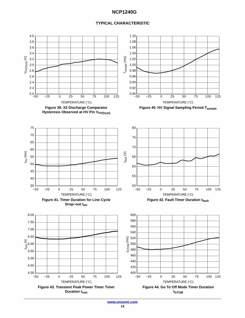
TYPICAL CHARACTERISTIC
Figure 39. X2 Discharge ComparatorHysteresis Observed at HV Pin VHV(hyst)
VH
V(h
yst) (
V)
TEMPERATURE (°C)
−50 −25 0 25 50 75 100 125 −50 −25 0 25 50 75 100 125
Figure 40. HV Signal Sampling Period Tsample
TEMPERATURE (°C)
T sam
ple
(ms)
−50 −25 0 25 50 75 100 125
Figure 41. Timer Duration for Line CycleDrop−out tHV
t HV (
ms)
TEMPERATURE (°C)
−50 −25 0 25 50 75 100 125
Figure 42. Fault Timer Duration tfault
t faul
t (V
)
TEMPERATURE (°C)
−50 −25 0 25 50 75 100 125
Figure 43. Transient Peak Power Timer TimerDuration ttran
t tran
(s)
TEMPERATURE (°C)
−50 −25 0 25 50 75 100 125
Figure 44. Go To Off Mode Timer DurationtGTOM
t GT
OM
(m
s)
TEMPERATURE (°C)
2.0
2.2
2.4
2.6
2.8
3.0
3.2
3.4
3.6
3.8
4.0
0.90
0.92
0.94
0.96
0.98
1.00
1.02
1.04
1.06
1.08
1.10
35
40
45
50
55
60
65
70
75
50
55
60
65
70
75
80
4.00
4.50
5.00
5.50
6.00
6.50
7.00
7.50
8.00
400
420
440
460
480
500
520
540
560
580
600
NCP1240G
www.onsemi.com15
APPLICATION INFORMATION
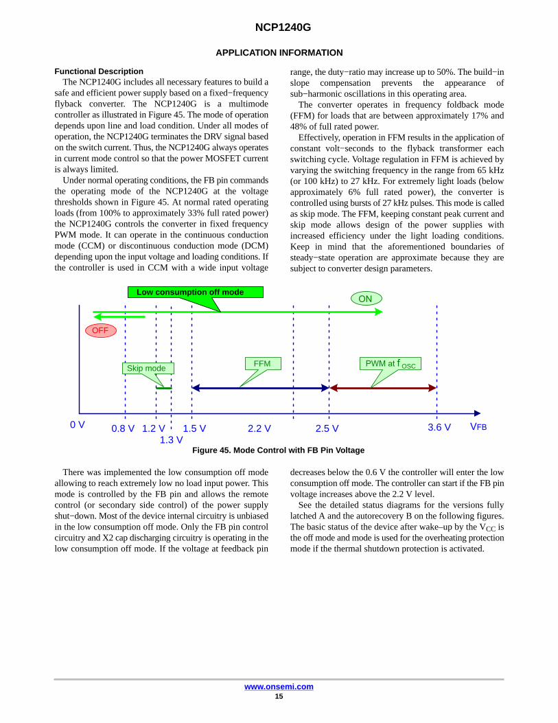
Functional DescriptionThe NCP1240G includes all necessary features to build a
safe and efficient power supply based on a fixed−frequencyflyback converter. The NCP1240G is a multimodecontroller as illustrated in Figure 45. The mode of operationdepends upon line and load condition. Under all modes ofoperation, the NCP1240G terminates the DRV signal basedon the switch current. Thus, the NCP1240G always operatesin current mode control so that the power MOSFET currentis always limited.
Under normal operating conditions, the FB pin commandsthe operating mode of the NCP1240G at the voltagethresholds shown in Figure 45. At normal rated operatingloads (from 100% to approximately 33% full rated power)the NCP1240G controls the converter in fixed frequencyPWM mode. It can operate in the continuous conductionmode (CCM) or discontinuous conduction mode (DCM)depending upon the input voltage and loading conditions. Ifthe controller is used in CCM with a wide input voltage
range, the duty−ratio may increase up to 50%. The build−inslope compensation prevents the appearance ofsub−harmonic oscillations in this operating area.
The converter operates in frequency foldback mode(FFM) for loads that are between approximately 17% and48% of full rated power.
Effectively, operation in FFM results in the application ofconstant volt−seconds to the flyback transformer eachswitching cycle. Voltage regulation in FFM is achieved byvarying the switching frequency in the range from 65 kHz(or 100 kHz) to 27 kHz. For extremely light loads (belowapproximately 6% full rated power), the converter iscontrolled using bursts of 27 kHz pulses. This mode is calledas skip mode. The FFM, keeping constant peak current andskip mode allows design of the power supplies withincreased efficiency under the light loading conditions.Keep in mind that the aforementioned boundaries ofsteady−state operation are approximate because they aresubject to converter design parameters.
VFB3.6 V2.2 V 2.5 V1.5 V1.3 V
1.2 V0.8 V
FFM PWM at f OSCSkip mode
0 V
Low consumption off mode
OFF
Figure 45. Mode Control with FB Pin Voltage
ON
There was implemented the low consumption off modeallowing to reach extremely low no load input power. Thismode is controlled by the FB pin and allows the remotecontrol (or secondary side control) of the power supplyshut−down. Most of the device internal circuitry is unbiasedin the low consumption off mode. Only the FB pin controlcircuitry and X2 cap discharging circuitry is operating in thelow consumption off mode. If the voltage at feedback pin
decreases below the 0.6 V the controller will enter the lowconsumption off mode. The controller can start if the FB pinvoltage increases above the 2.2 V level.
See the detailed status diagrams for the versions fullylatched A and the autorecovery B on the following figures.The basic status of the device after wake–up by the VCC isthe off mode and mode is used for the overheating protectionmode if the thermal shutdown protection is activated.

NCP1240G
www.onsemi.com16
Figure 46. Operating Status Diagram for the Fully Latched Versions A and E of the Device
Extra L
ow
Co
nsu
mp
tion
Pow
er On
Reset
Latch=0
Off M
ode
Latch=X
Latch
Latch=1
Stop
Reset
Latch=0
BO
+T
SD
BO
+T
SD
Soft
Start
Running
Skip
mode
Skip in
Skip out
SS
end
BO
BO
AC
present+
discharged
Efficien
t op
erating
mo
de
Dyn
amic S
elf−Su
pp
ly
(if not enoughgh auxiliary voltage ispresent)
Reg
ulated
Self−S
up
ply
VC
Cfault
X2 cap
Discharge
Latch=0
No A
C
VH
V > V
HV
(NO
AC
)
VC
C >
VC
Creset
VCC > VCCreset
(VF
B < V
OF
F ) * GT
OM
timer*(V
CC
> V
CC
off )(VF
B > V
ON
)*Latch
(VFB > VON)*Latch
OV
P+
OT
P+
VC
Covp +
VC
Sstop
(VILIM +MaxDC)*tfault
VC
C >
VC
Coff
(VC
C >
VC
Con )*B
O
(VC
C <
VC
Coff
(VC
C <
VC
Coff

NCP1240G
www.onsemi.com17
Figure 47. Operating Status Diagram for the Autorecovery Versions B and F of the Device
Extra L
ow
Co
nsu
mp
tion
Pow
er On
Reset
Latch=0
AutoR
ec=0
X2 cap
DischargeLatch=
0A
utoRec=
0
Off M
ode
Latch=X
AutoR
ec=X
Latch
Latch=1
Stop
Reset
Latch=0
AutoR
ec=0
Autorecovery
Latch
AutoR
ec=1
BO
+T
SD
BO
+T
SD
Soft
Start
Running
Skip
mode
Skip in
Skip out
SS
end
BO
BO
BO
AC
present+
discharged
Efficien
t op
erating
mo
de
Reg
ulated
Self−S
up
ply
Dyn
amic S
elf−Su
pp
ly (if not enough auxiliary voltage is
present)
VC
C
fault
No A
C
(VF
B < V
OF
F ) * GT
OM
timer*(V
CC
> V
CC
off )
VH
V > V
HV
(NO
AC
)
VC
C <
VC
Creset
VCC > VCCreset
(VFB > VON)*Latch
(VF
B > V
ON
)*Latch*AutoR
ec
(VF
B > V
ON
)*AutoR
ec
OV
P+
OT
P+
VC
Covp
BO+tautorec
VC
Sstop
VC
C <
VC
Coff
(VILIM + MaxDC)*tfault
(VC
C >
VC
Con )*B
O
VC
C <
VC
Coff
VC
C >
VC
Coff

NCP1240G
www.onsemi.com18
The information about the fault (permanent Latch orAutorecovery) is kept during the low consumption off modedue the safety reason. The reason is not to allow unlatch thedevice by the remote control being in off mode.
Start−up of the ControllerAt start−up, the current source turns on when the voltage
on the HV pin is higher than VHV(min), and turns off whenVCC reaches VCC(on), then turns on again when VCC reachesVCC(min), until the input voltage is high enough to ensure aproper start−up, i.e. when VHV reaches VHV(start). Thecontroller actually starts the next time VCC reaches VCC(on).The controller then delivers pulses, starting with a soft−startperiod tSSTART during which the peak current linearlyincreases before the current−mode control takes over.
Even though the Dynamic Self−Supply is able to maintainthe VCC voltage between VCC(on) and VCC(min) by turningthe HV start−up current source on and off, it can only be usedin light load condition, otherwise the power dissipation onthe die would be too much. As a result, an auxiliary voltagesource is needed to supply VCC during normal operation.
The Dynamic Self−Supply is useful to keep the controlleralive when no switching pulses are delivered, e.g. inbrown−out condition, or to prevent the controller fromstopping during load transients when the VCC might drop.The NCP1240G accepts a supply voltage as high as 28 V,with an overvoltage threshold VCC(ovp) that latches thecontroller off.
Figure 48. VCC Start−up Timing Diagram
time
VHV
time
VCC
time
DRV
VHV(start)
V HV(min)
VCC(on)
V CC(min)
HV current
source = Istart1
HV current
source = Istart2
Waits next VCC(on)before starting
VCC(inhibit)

NCP1240G
www.onsemi.com19
For safety reasons, the start−up current is lowered whenVCC is below VCC(inhibit), to reduce the power dissipation incase the VCC pin is shorted to GND (in case of VCC capacitorfailure, or external pull−down on VCC to disable thecontroller). There is only one condition for which the currentsource doesn’t turn on when VCC reaches VCC(inhibit): thevoltage on HV pin is too low (below VHV(min)).
HV Sensing of Rectified AC VoltageThe NCP1240G features on its HV pin a true ac line
monitoring circuitry. It includes a minimum start−up
threshold and an autorecovery brown−out protection; bothof them independent of the ripple on the input voltage. It isallowed only to work with an unfiltered, rectified ac input toensure the X2 capacitor discharge function as well, which isdescribed in following. The brown−out protectionthresholds are fixed, but they are designed to fit most of thestandard ac−dc conversion applications.
When the input voltage goes below VHV(stop), abrown−out condition is detected, and the controller stops.The HV current source maintains VCC at VCC(min) level untilthe input voltage is back above VHV(start).

NCP1240G
www.onsemi.com21
time
VCC
time
DRV
VCC(on)
VCC(off)
Overloadapplied
time
VOUT
VOUT(typ)
Controllerlatches off
Autorecoverytimer starts
Controllerrestarts
VCC(min)
tautorecAutorecoverytimer elapses
Waits nextVccON before
Figure 50. VCC Collapses After Overload and Its Recovery

NCP1240G
www.onsemi.com22
time
HV stop
time
VCC
time
DRV
VCC(on)
VCC(min)
Waits nextVccON before
starting
time
VHVHV timer elapsed
VHV(start)
VHV(stop)
Brown−outconditionresets the
Internal Latch
tHV
Brown−outdetected
Spike induced byresidual energy in
Figure 51. Ac Line Drop−out Timing Diagram with Parasitic Spike
When VHV crosses the VHV(start) threshold, the controllercan start immediately. When it crosses VHV(stop), it triggersa timer of duration tHV, this ensures that the controllerdoesn’t stop in case of line cycle drop−out. The device restartafter the ac line voltage drop-out is protected to the parasiticrestart initiated e.g. the spikes induced at HV pin
immediately after the device is stopped by the residualenergy in the EMI filter. The device restart is allowed onlyafter the 1st watch dog signal event. The basic principle isshown at Figure 49 and detail of the device restart is shownat Figure 52.

NCP1240G
www.onsemi.com23
Figure 52. Detailed Timing Diagram of the Device Restart After the Short ac Line Drop−out

NCP1240G
www.onsemi.com24
X2 Cap Discharge FeatureThe X2 capacitor discharging feature is offered by usage
of the NCP1240G. This feature saves approximately 16 mW− 25 mW input power depending on the EMI filter X2capacitors volume and it saves the external componentscount as well. The discharge feature is ensured via thestart−up current source with a dedicated control circuitry forthis function. The X2 capacitors are being discharged bycurrent defined as Istart2 when this discharge event isdetected.
There is used a dedicated structure called ac line unplugdetector inside the X2 capacitor discharge control circuitry.See the Figure 53 for the block diagram for this structure andFigures 54, 55, 56 and 57 for the timing diagrams. The basicidea of ac line unplug detector lies in comparison of thedirect sample of the high voltage obtained via the highvoltage sensing structure with the delayed sample of the highvoltage. The delayed signal is created by the sample & holdstructure.
The comparator used for the comparison of these signalsis without hysteresis inside. The resolution between theslopes of the ac signal and dc signal is defined by thesampling time TSAMPLE and additional internal offset NOS.These parameters ensure the noise immunity as well. Theadditional offset is added to the picture of the sampled HVsignal and its analog sum is stored in the C1 storagecapacitor. If the voltage level of the HV sensing structureoutput crosses this level the comparator CMP output signalresets the detection timer and no dc signal is detected. Theadditional offset NOS can be measured as the VHV(hyst) onthe HV pin. If the comparator output produces pulses itmeans that the slope of input signal is higher than setresolution level and the slope is positive. If the comparatoroutput produces the low level it means that the slope of inputsignal is lower than set resolution level or the slope isnegative. There is used the detection timer which is reset byany edge of the comparator output. It means if no edgecomes before the timer elapses there is present only dc signalor signal with the small ac ripple at the HV pin. This type ofthe ac detector detects only the positive slope, which fulfilsthe requirements for the ac line presence detection.
In case of the dc signal presence on the high voltage input,the direct sample of the high voltage obtained via the highvoltage sensing structure and the delayed sample of the highvoltage are equivalent and the comparator produces the lowlevel signal during the presence of this signal. No edges arepresent at the output of the comparator, that’s why thedetection timer is not reset and dc detect signal appears.
The minimum detectable slope by this ac detector is givenby the ration between the maximum hysteresis observed atHV pin VHV(hyst),max and the sampling time:
Smin �VHV(hyst),max
Tsample
(eq. 1)
Than it can be derived the relationship between theminimum detectable slope and the amplitude and frequencyof the sinusoidal input voltage:
Vmax �VHV(hyst),max
2 � � � f � Tsample
�5
2 � � � 35 � 1 � 10−3 (eq. 2)
� 22.7 V
The minimum detectable AC RMS voltage is 16 V atfrequency 35 Hz, if the maximum hysteresis is 5 V andsampling time is 1 ms.
The X2 capacitor discharge feature is available in anycontroller operation mode to ensure this safety feature. Thedetection timer is reused for the time limiting of thedischarge phase, to protect the device against overheating.The discharging process is cyclic and continues until the acline is detected again or the voltage across the X2 capacitoris lower than VHV(min). This feature ensures to dischargequite big X2 capacitors used in the input line filter to the safelevel. It is important to note that it is not allowed toconnect HV pin to any dc voltage due this feature. e.g.directly to bulk capacitor.
During the HV sensing or X2 cap discharging the VCC netis kept above the VCC(off) voltage by the Self−Supply in anymode of device operation to supply the control circuitry.During the discharge sequence is not allowed to start−up thedevice.

NCP1240G
www.onsemi.com25
Figure 53. The ac Line Unplug Detector Structure Used for X2 Capacitor Discharge System
Figure 54. The ac Line Unplug Detector Timing Diagram
NCP1240G
www.onsemi.com26
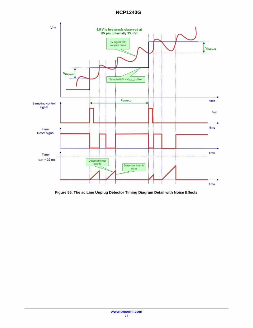
Figure 55. The ac Line Unplug Detector Timing Diagram Detail with Noise Effects

NCP1240G
www.onsemi.com27
Figure 56. HV Pin ac Input Timing Diagram with X2 Capacitor Discharge Sequence When the Application isUnplugged Under Extremely Low Line Condition

NCP1240G
www.onsemi.com28
Figure 57. HV Pin ac Input Timing Diagram with X2 Capacitor Discharge Sequence When the Application isUnplugged Under High Line Condition
The Low Consumption Off ModeThere was implemented the low consumption off mode
allowing to reach extremely low no load input power asdescribed in previous chapters. If the voltage at feedback pindecreases below the 0.6 V the controller enters the off mode.The internal VCC is turned−off, the IC consumes extremelylow VCC current and only the voltage at external VCCcapacitor is maintained by the Self−Supply circuit. TheSelf−Supply circuit keeps the VCC voltage at the VCC(reg)level. The supply for the FB pin watch dog circuitry and FBpin bias is provided via the low consumption current sourcesfrom the external VCC capacitor. The controller can onlystart, if the FB pin voltage increases above the 2.2 V level.See Figure 58 for timing diagrams.
Only the X2 cap discharge and Self−Supply features isenabled in the low consumption off mode. The X2 capdischarging feature is enable due the safety reasons and theSelf−Supply is enabled to keep the VCC supply, but onlyvery low VCC consumption appears in this mode. Any otherfeatures are disabled in this mode.
The information about the latch status of the device is keptin the low consumption off mode and this mode is used forthe TSD protection as well. The protection timerGoToOffMode tGTOM is used to protect the applicationagainst the false activation of the low consumption off modeby the fast drop outs of the FB pin voltage below the 0.6 Vlevel. E.g. in case when is present high FB pin voltage rippleduring the skip mode.
NCP1240G
www.onsemi.com29
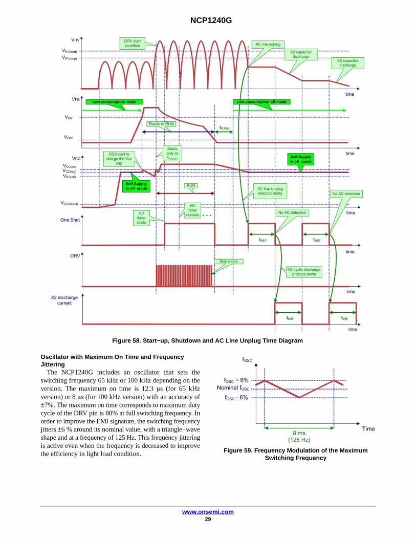
Figure 58. Start−up, Shutdown and AC Line Unplug Time Diagram
Oscillator with Maximum On Time and FrequencyJittering
The NCP1240G includes an oscillator that sets theswitching frequency 65 kHz or 100 kHz depending on theversion. The maximum on time is 12.3 �s (for 65 kHzversion) or 8 �s (for 100 kHz version) with an accuracy of±7%. The maximum on time corresponds to maximum dutycycle of the DRV pin is 80% at full switching frequency. Inorder to improve the EMI signature, the switching frequencyjitters ±6 % around its nominal value, with a triangle−waveshape and at a frequency of 125 Hz. This frequency jitteringis active even when the frequency is decreased to improvethe efficiency in light load condition. Figure 59. Frequency Modulation of the Maximum
Switching Frequency

NCP1240G
www.onsemi.com30
Low Load Operation Modes: Frequency FoldbackMode (FFM) and Skip Mode
In order to improve the efficiency in light load conditions,the frequency of the internal oscillator is linearly reducedfrom its nominal value down to fOSC(min). This frequencyfoldback starts when the voltage on FB pin goes below
VFB(foldS), and is complete when VFB reaches VFB(foldE).The maximum on−time duration control is kept during thefrequency foldback mode to provide the natural transformercore anti−saturation protection. The frequency jittering isstill active while the oscillator frequency decreases as well.
Figure 60. Frequency Foldback Mode Characteristic
When the FB voltage reaches Vskip(in) while decreasing,skip mode is activated: the driver stops, and the internalconsumption of the controller is decreased. While VFB is
below Vskip(out), the controller remains in this state; but assoon as VFB crosses the skip out threshold, the DRV pinstarts to pulse again.
Figure 61. Skip Mode Timing Diagram

NCP1240G
www.onsemi.com31
Figure 62. Technique Preventing Short Pulses in Skip Mode
Clamped DriverThe supply voltage for the NCP1240G can be as high as
28 V, but most of the MOSFETs that will be connected to theDRV pin cannot accept more than 20 V on their gate. Thedriver pin is therefore clamped safely below 16 V. Thisdriver has a typical capability of 500 mA for source currentand 800 mA for sink current.
Current−Mode Control With Slope Compensation andSoft−Start
NCP1240G is a current−mode controller, which meansthat the FB voltage sets the peak current flowing in theinductance and the MOSFET. This is done through a PWMcomparator: the current is sensed across a resistor and the
resulting voltage is applied to the CS pin. It is applied to oneinput of the PWM comparator through a 250 ns LEB block.On the other input the FB voltage divided by 5 sets thethreshold: when the voltage ramp reaches this threshold, theoutput driver is turned off. The maximum value for thecurrent sense is 0.7 V, and it is set by a dedicated comparator.
Each time the controller is starting, i.e. the controller wasoff and starts – or restarts – when VCC reaches VCC(on), asoft−start is applied: the current sense setpoint is increasedby 15 discrete steps from 0 (the minimum level can behigher than 0 because of the LEB and propagation delay)until it reaches VILIM (after a duration of tSSTART), or untilthe FB loop imposes a setpoint lower than the one imposedby the soft−start (the two comparators outputs are OR’ed).
NCP1240G
www.onsemi.com32
Figure 63. Soft−Start Feature
Under some conditions, like a winding short−circuit forinstance, not all the energy stored during the on time istransferred to the output during the off time, even if the ontime duration is at its minimum (imposed by the propagationdelay of the detector added to the LEB duration). As a result,the current sense voltage keeps on increasing above VILIM,because the controller is blind during the LEB blankingtime. Dangerously high current can grow in the system ifnothing is done to stop the controller. That’s what theadditional comparator, that senses when the current sensevoltage on CS pin reaches VCS(stop) ( = 1.5 x VILIM ), does:the controller enters the protection mode as soon as thiscomparator toggles four times consecutively.
In order to allow the NCP1240G to operate in CCM witha duty cycle above 50%, the fixed slope compensation isinternally applied to the current−mode control. The slopeappearing on the internal voltage setpoint for the PWMcomparator is −32.5 mV/�s typical for the 65 kHz version,and −50 mV/�s for the 100 kHz version. The slopecompensation can be observable as a value of the peakcurrent at CS pin.
The internal slope compensation circuitry uses a sawtoothsignal synchronized with the internal oscillator is subtractedfrom the FB voltage divided by KFB.

NCP1240G
www.onsemi.com33
Figure 64. Slope Compensation Block Diagram
Figure 65. Slope Compensation Timing Diagram
Internal Overpower ProtectionThe power delivered by a flyback power supply is
proportional to the square of the peak current indiscontinuous conduction mode:
POUT �1
2� � � LP � FSW � IP
2 (eq. 3)
Unfortunately, due to the inherent propagation delay ofthe logic, the actual peak current is higher at high inputvoltage than at low input voltage, leading to a significantdifference in the maximum output power delivered by thepower supply.

NCP1240G
www.onsemi.com34
Figure 66. Needs for Line Compensation For True Overpower Protection
To compensate this and have an accurate overpowerprotection, an offset proportional to the input voltage isadded on the CS signal by turning on an internal currentsource: by adding an external resistor in series between thesense resistor and the CS pin, a voltage offset is createdacross it by the current. The compensation can be adjustedby changing the value of the resistor.
But this offset is unwanted to appear when the currentsense signal is small, i.e. in light load conditions, where itwould be in the same order of magnitude. Therefore thecompensation current is only added when the FB voltage ishigher than VFB(OPCE). However, because the HV pin isbeing connected to ac voltage, there is needed an additionalcircuitry to read or at least closely estimate the actual voltageon the bulk capacitor.
Figure 67. Overpower Protection Current Relation to Feedback Voltage
Figure 68. Overpower Protection Current Relation to Peak of Rectified Input Line AC voltage

NCP1240G
www.onsemi.com35
Figure 69. Block Schematic of Overpower Protection Circuit
Div
isio
n ra
tio 4
Inte
rnal
res
itanc
e 40
k
FB
CS
Rfb
1
Rfb
2R
fb3
PWM_CMP
LEB 250ns
Vfb(reg)
PWM
I generator
Ictrl
Vfb
(opc
f)
FBbuffer
A/D 3 bitConverter
Peak detector+
3 bit
Register
HV
CMP
Lo frq OSCOut sq
Detection timerreset
R1
DC detect
Sample & Hold
R2
Q1
C1Nos
OP
C c
ontr
ol
Positive slope

NCP1240G
www.onsemi.com36
A 3 bit A/D converter with the peak detector senses the acinput, and its output is periodically sampled and reset, inorder to follow closely the input voltage variations. Thesample and reset events are given by the output from the acline unplug detector. The sensed HV pin voltage peak valueis validated when no HV edges from comparator are presentafter last falling edge during two sample clocks. SeeFigure 70 for details.
Overcurrent Protection with Fault timerThe overload protection depends only on the current
sensing signal, making it able to work with any transformer,even with very poor coupling or high leakage inductance.
When an overcurrent event occurs on the output of thepower supply, the FB loop asks for more power than thecontroller can deliver, and the CS setpoint reaches VILIM.
When this event occurs, an internal tfault timer is started:once the timer times out, DRV pulses are stopped and thecontroller is either latched off (latched protection, options Aand E) or this latch is released by the autorecovery mode(options B and F), the controller tries to restart after tautorec.Other possibilities of the latch release are the brown−outcondition or the VCC power on reset. The timer is reset whenthe CS setpoint goes back below VILIM before the timerelapses. The fault timer is also started if the driver signal isreset by the maximum on time. The controller also enters thesame protection mode if the voltage on the CS pin reaches1.5 times the maximum internal setpoint VCS(stop) (allows todetect winding short−circuits) or there appears low VCCsupply. See Figures 71 and 72 for the timing diagram.
In autorecovery mode if the fault has gone, the supplyresumes operation; if not, the system starts a new burst cycle.
NCP1240G
www.onsemi.com37
time
VHVSAMPLE
time
ComparatorOutput
TSAMPLE
2nd sample clockpulse after last
HV edge initiatesthe watch dog
signal
VHV(hyst)
time
Sample clock
time
Watch dogsignal
1st HV edgeresets the watchdog and starts
the peakdetection of HV
pin signal
SampleSample
Reset
2nd sample clockpulse after last
HV edge initiatesthe watch dog
signal
time
Peak detector
time
IOPC
Figure 70. Overpower Compensation Timing Diagram
Reset
NCP1240G
www.onsemi.com38
PROTECTION MODES AND THE LATCH MODE RELEASES
Event Timer Protection Next Device Status Release to Normal Operation Mode
OvercurrentVILIM > 0.7 V
Fault timer Latch Brown−outVCC < VCC(reset)
Peak powerVILIM > 0.5 V
Transient timer Latch Brown−outVCC < VCC(reset)
Maximum on time Fault timer Latch Brown−outVCC < VCC(reset)
Winding shortVsense > VCS(stop)
4consecutive pulses Latch Brown−outVCC < VCC(reset)
Low supplyVCC < VCC(off)
10 �s timer Latch Autorecovery – B and F versionsBrown−out
VCC < VCC(reset)
External OTP, OVP 55 �s (35 �s at 100 kHz) Latch Brown−outVCC < VCC(reset)
High supplyVCC > VCC(ovp)
10 �s timer Latch Brown−outVCC < VCC(reset)
Brown−outVHV < VHV(stop)
HV timer Device stops (VHV > VHV(start)) & (VCC > VCC(on))
Internal TSD 10 �s timer Device stops, HV start−upcurrent source stops
(VHV > VHV(start)) & (VCC > VCC(on)) & TSDb
Off modeVFB < VOFF
150 ms timer Device stops and internalVCC is turned off
(VHV > VHV(start)) & (VCC > VCC(on)) & (VFB > VON)

NCP1240G
www.onsemi.com39
Figure 71. Latched Timer−Based Overcurrent Protection (Option G)
VCC(on)
VCC(min)
Duel−Level Overcurrent ProtectionFor some applications (e.g. limited power supplies), it is
necessary that the controller maintains regulation while ithas detected a first level of overload. This is to authorize atransient peak power higher than the maximum continuousoutput power. This is implemented by adding another
comparator whose threshold is VCS(tran), a CS voltage levellower than VILIM, which starts the counting of another timer,with a duration ttran longer than tfault (3.6 s is the typicalvalue). If the timer reaches its maximum duration, thecontroller enters protection mode which is latched orautorecovery released depending on the option.

NCP1240G
www.onsemi.com40
Figure 72. Too Long Transient Peak Power Delivery
If the conditions change from transient power delivery to overload, the overload timer starts to count. The timing diagramcould look like the one in Figure 73.

NCP1240G
www.onsemi.com41
Figure 73. Transient Peak Power Followed by Overload
NCP1240G
www.onsemi.com42
Latch−Off Input
Figure 74. Latch Detection Schematic
The Latch pin is dedicated to the latch−off function: itincludes two levels of detection that define a workingwindow, between a high latch and a low latch: within thesetwo thresholds, the controller is allowed to run, but as soonas either the low or the high threshold is crossed, thecontroller is latched off. The lower threshold is intended tobe used with an NTC thermistor, thanks to an internal currentsource INTC.
An active clamp prevents the voltage from reaching thehigh threshold if it is only pulled up by the INTC current. Toreach the high threshold, the pull−up current has to be higherthan the pull−down capability of the clamp (typically1.5 mA at VOVP).
To avoid any false triggering, spikes shorter than 50 �s(for the high latch and 65 kHz version) or 350 �s (for the lowlatch) are blanked and only longer signals can actually latchthe controller.
Reset occurs when a brown−out condition is detected orthe VCC is cycled down to a reset voltage, which in a realapplication can only happen if the power supply isunplugged from the ac line.
Upon startup, the internal references take some timebefore being at their nominal values; so one of thecomparators could toggle even if it should not. Therefore theinternal logic does not take the latch signal into accountbefore the controller is ready to start: once VCC reachesVCC(on), the latch pin High latch state is taken into accountand the DRV switching starts only if it is allowed; whereasthe Low latch (typically sensing an over temperature) istaken into account only after the soft−start is finished. Inaddition, the NTC current is doubled to INTC(SSTART) duringthe soft−start period, to speed up the charging of the Latchpin capacitor. The maximum value of Latch pin capacitor isgiven by the following formula (The standard start−upcondition is considered and the NTC current is neglected):
CLATCH max �tSSTART min � INTC(SSTART) min
Vclamp0 min
�8.0 � 10−3 � 130 � 10−6
1.0F � 1.04 �F (eq. 4)

NCP1240G
www.onsemi.com43
Figure 75. Latch Timing Diagram
VCC(on)
VCC(min)
Temperature ShutdownThe NCP1240 includes a temperature shutdown
protection with a trip point typically at 150°C and the typicalhysteresis of 30°C. When the temperature rises above thehigh threshold, the controller stops switchinginstantaneously, and goes to the off mode with extremely
low power consumption. There is kept the VCC supply tokeep the TSD information. When the temperature fallsbelow the low threshold, the start−up of the device is enabledagain, and a regular start−up sequence takes place. See thestatus diagrams at the Figure 46.
ORDERING INFORMATION
Ordering Part No. Overload Protection Switching Frequency Package Shipping†
NCP1240GD065R2G Latched 65 kHz SOIC−7(Pb−Free)
2500 / Tape & Reel
†For information on tape and reel specifications, including part orientation and tape sizes, please refer to our Tape and Reel PackagingSpecifications Brochure, BRD8011/D.
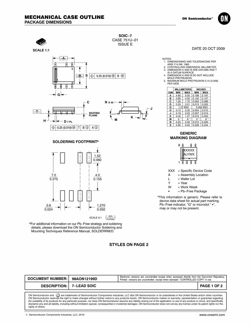
SOIC−7CASE 751U−01
ISSUE EDATE 20 OCT 2009
SEATINGPLANE
14
58
R
J
X 45�
K
NOTES:1. DIMENSIONING AND TOLERANCING PER
ANSI Y14.5M, 1982.2. CONTROLLING DIMENSION: MILLIMETER.3. DIMENSION A AND B ARE DATUMS AND T
IS A DATUM SURFACE.4. DIMENSION A AND B DO NOT INCLUDE
MOLD PROTRUSION.5. MAXIMUM MOLD PROTRUSION 0.15 (0.006)
PER SIDE.
S
DH
C
SCALE 1:1
DIMA
MIN MAX MIN MAXINCHES
4.80 5.00 0.189 0.197
MILLIMETERS
B 3.80 4.00 0.150 0.157C 1.35 1.75 0.053 0.069D 0.33 0.51 0.013 0.020G 1.27 BSC 0.050 BSCH 0.10 0.25 0.004 0.010J 0.19 0.25 0.007 0.010K 0.40 1.27 0.016 0.050M 0 8 0 8 N 0.25 0.50 0.010 0.020S 5.80 6.20 0.228 0.244
−A−
−B−
G
MBM0.25 (0.010)
−T−
BM0.25 (0.010) T S A S
M
XXX = Specific Device CodeA = Assembly LocationL = Wafer LotY = YearW = Work Week� = Pb−Free Package
GENERICMARKING DIAGRAM
7 PL� � � �
*This information is generic. Please refer todevice data sheet for actual part marking.Pb−Free indicator, “G” or microdot “ �”,may or may not be present.
XXXXXALYWX
�1
8
STYLES ON PAGE 2
1.520.060
7.00.275
0.60.024
1.2700.050
4.00.155
� mminches
�SCALE 6:1
*For additional information on our Pb−Free strategy and solderingdetails, please download the ON Semiconductor Soldering andMounting Techniques Reference Manual, SOLDERRM/D.
SOLDERING FOOTPRINT*
MECHANICAL CASE OUTLINE
PACKAGE DIMENSIONS
ON Semiconductor and are trademarks of Semiconductor Components Industries, LLC dba ON Semiconductor or its subsidiaries in the United States and/or other countries.ON Semiconductor reserves the right to make changes without further notice to any products herein. ON Semiconductor makes no warranty, representation or guarantee regardingthe suitability of its products for any particular purpose, nor does ON Semiconductor assume any liability arising out of the application or use of any product or circuit, and specificallydisclaims any and all liability, including without limitation special, consequential or incidental damages. ON Semiconductor does not convey any license under its patent rights nor therights of others.
98AON12199DDOCUMENT NUMBER:
DESCRIPTION:
Electronic versions are uncontrolled except when accessed directly from the Document Repository.Printed versions are uncontrolled except when stamped “CONTROLLED COPY” in red.
PAGE 1 OF 27−LEAD SOIC
© Semiconductor Components Industries, LLC, 2019 www.onsemi.com

SOIC−7CASE 751U−01
ISSUE EDATE 20 OCT 2009
STYLE 4:PIN 1. ANODE
2. ANODE3. ANODE4. ANODE5. ANODE6. ANODE7. NOT USED8. COMMON CATHODE
STYLE 1:PIN 1. EMITTER
2. COLLECTOR3. COLLECTOR4. EMITTER5. EMITTER6.7. NOT USED8. EMITTER
STYLE 2:PIN 1. COLLECTOR, DIE, #1
2. COLLECTOR, #13. COLLECTOR, #24. COLLECTOR, #25. BASE, #26. EMITTER, #27. NOT USED8. EMITTER, #1
STYLE 3:PIN 1. DRAIN, DIE #1
2. DRAIN, #13. DRAIN, #24. DRAIN, #25. GATE, #26. SOURCE, #27. NOT USED8. SOURCE, #1
STYLE 6:PIN 1. SOURCE
2. DRAIN3. DRAIN4. SOURCE5. SOURCE6.7. NOT USED8. SOURCE
STYLE 5:PIN 1. DRAIN
2. DRAIN3. DRAIN4. DRAIN5.6.7. NOT USED8. SOURCE
STYLE 7:PIN 1. INPUT
2. EXTERNAL BYPASS3. THIRD STAGE SOURCE4. GROUND5. DRAIN6. GATE 37. NOT USED8. FIRST STAGE Vd
STYLE 8:PIN 1. COLLECTOR (DIE 1)
2. BASE (DIE 1)3. BASE (DIE 2)4. COLLECTOR (DIE 2)5. COLLECTOR (DIE 2)6. EMITTER (DIE 2)7. NOT USED8. COLLECTOR (DIE 1)
STYLE 9:PIN 1. EMITTER (COMMON)
2. COLLECTOR (DIE 1)3. COLLECTOR (DIE 2)4. EMITTER (COMMON)5. EMITTER (COMMON)6. BASE (DIE 2)7. NOT USED8. EMITTER (COMMON)
STYLE 10:PIN 1. GROUND
2. BIAS 13. OUTPUT4. GROUND5. GROUND6. BIAS 27. NOT USED8. GROUND
STYLE 11:PIN 1. SOURCE (DIE 1)
2. GATE (DIE 1)3. SOURCE (DIE 2)4. GATE (DIE 2)5. DRAIN (DIE 2)6. DRAIN (DIE 2)7. NOT USED8. DRAIN (DIE 1)
ON Semiconductor and are trademarks of Semiconductor Components Industries, LLC dba ON Semiconductor or its subsidiaries in the United States and/or other countries.ON Semiconductor reserves the right to make changes without further notice to any products herein. ON Semiconductor makes no warranty, representation or guarantee regardingthe suitability of its products for any particular purpose, nor does ON Semiconductor assume any liability arising out of the application or use of any product or circuit, and specificallydisclaims any and all liability, including without limitation special, consequential or incidental damages. ON Semiconductor does not convey any license under its patent rights nor therights of others.
98AON12199DDOCUMENT NUMBER:
DESCRIPTION:
Electronic versions are uncontrolled except when accessed directly from the Document Repository.Printed versions are uncontrolled except when stamped “CONTROLLED COPY” in red.
PAGE 2 OF 27−LEAD SOIC
© Semiconductor Components Industries, LLC, 2019 www.onsemi.com

onsemi, , and other names, marks, and brands are registered and/or common law trademarks of Semiconductor Components Industries, LLC dba “onsemi” or its affiliatesand/or subsidiaries in the United States and/or other countries. onsemi owns the rights to a number of patents, trademarks, copyrights, trade secrets, and other intellectual property.A listing of onsemi’s product/patent coverage may be accessed at www.onsemi.com/site/pdf/Patent−Marking.pdf. onsemi reserves the right to make changes at any time to anyproducts or information herein, without notice. The information herein is provided “as−is” and onsemi makes no warranty, representation or guarantee regarding the accuracy of theinformation, product features, availability, functionality, or suitability of its products for any particular purpose, nor does onsemi assume any liability arising out of the application or useof any product or circuit, and specifically disclaims any and all liability, including without limitation special, consequential or incidental damages. Buyer is responsible for its productsand applications using onsemi products, including compliance with all laws, regulations and safety requirements or standards, regardless of any support or applications informationprovided by onsemi. “Typical” parameters which may be provided in onsemi data sheets and/or specifications can and do vary in different applications and actual performance mayvary over time. All operating parameters, including “Typicals” must be validated for each customer application by customer’s technical experts. onsemi does not convey any licenseunder any of its intellectual property rights nor the rights of others. onsemi products are not designed, intended, or authorized for use as a critical component in life support systemsor any FDA Class 3 medical devices or medical devices with a same or similar classification in a foreign jurisdiction or any devices intended for implantation in the human body. ShouldBuyer purchase or use onsemi products for any such unintended or unauthorized application, Buyer shall indemnify and hold onsemi and its officers, employees, subsidiaries, affiliates,and distributors harmless against all claims, costs, damages, and expenses, and reasonable attorney fees arising out of, directly or indirectly, any claim of personal injury or deathassociated with such unintended or unauthorized use, even if such claim alleges that onsemi was negligent regarding the design or manufacture of the part. onsemi is an EqualOpportunity/Affirmative Action Employer. This literature is subject to all applicable copyright laws and is not for resale in any manner.
PUBLICATION ORDERING INFORMATIONTECHNICAL SUPPORTNorth American Technical Support:Voice Mail: 1 800−282−9855 Toll Free USA/CanadaPhone: 011 421 33 790 2910
LITERATURE FULFILLMENT:Email Requests to: [email protected]
onsemi Website: www.onsemi.com
Europe, Middle East and Africa Technical Support:Phone: 00421 33 790 2910For additional information, please contact your local Sales Representative
◊