Embed Size (px)
Citation preview
DATA SHEETwww.onsemi.com
© Semiconductor Components Industries, LLC, 2017
February, 2022 − Rev. 81 Publication Order Number:
NCP12400/D
Fixed Frequency CurrentMode Controller for FlybackConverters
NCP12400The NCP12400 is a new fixed−frequency current−mode controller
featuring the Dynamic Self−Supply. This function greatly simplifiesthe design of the auxiliary supply and the VCC capacitor by activatingthe internal startup current source to supply the controller duringstart−up, transients, latch, stand−by etc. This device contains a specialHV detector which detects the application unplug from the ac inputline and triggers the X2 discharge current. This HV structure allowsthe brown−out detection as well.
It features a timer−based fault detection that ensures the detection ofoverload and an adjustable compensation to help keep the maximumpower independent of the input voltage.
Due to frequency foldback, the controller exhibits excellentefficiency in light load condition while still achieving very lowstandby power consumption. Internal frequency jittering, rampcompensation, and a versatile latch input make this controller anexcellent candidate for the robust power supply designs.
A dedicated Off Mode allows to reach the extremely low no loadinput power consumption via “sleeping” whole device and thusminimize the power consumption of the control circuitry.
Features
• Fixed−Frequency Current−Mode Operation 65 kHz or 100 kHzFrequency Options
• Frequency Foldback then Skip Mode for Maximized Performance in Light Load and Standby Conditions
• Timer−Based Overload Protection with Latched (Option A) orAutorecovery (Option B) Operation
• High−Voltage Current Source with Brown−Out Detection andDynamic Self−Supply, Simplifying the Design of the VCC Circuitry
• Frequency Modulation for Softened EMI Signature• Adjustable Overpower Protection Dependant on the Mains Voltage• Fault Input for Overvoltage and Over Temperature Protection• VCC Operation up to 28 V, with Overvoltage Detection• 300/500 mA Source/Sink Drive Peak Current Capability• 4/10 ms Soft−Start• Internal Thermal Shutdown• No−Load Standby Power < 30 mW• X2 Capacitor in EMI Filter Discharging Feature• These are Pb−Free Devices
Typical Applications• Offline Adapters for Notebooks, LCD, and Printers• Offline Battery Chargers• Consumer Electronic Power Supplies• Auxiliary/Housekeeping Power Supplies• Offline Adapters for Notebooks
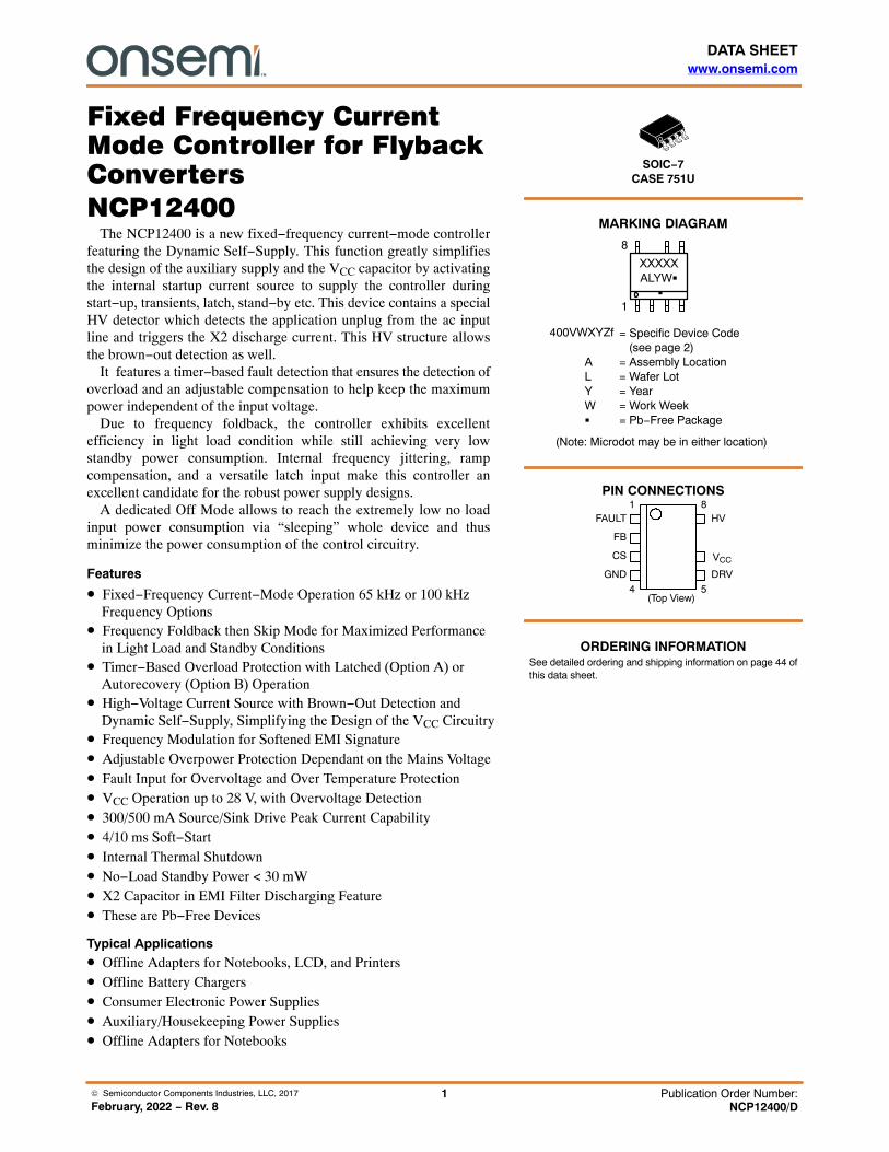
SOIC−7CASE 751U
MARKING DIAGRAM
(Note: Microdot may be in either location)
PIN CONNECTIONS
400VWXYZf
FAULT
FB
CS
GND DRV
HV
(Top View)
= Specific Device Code (see page 2)
A = Assembly LocationL = Wafer LotY = YearW = Work Week� = Pb−Free Package
XXXXXALYW�
�1
8
VCC
1
4
8
5
See detailed ordering and shipping information on page 44 ofthis data sheet.
ORDERING INFORMATION
NCP12400
www.onsemi.com2
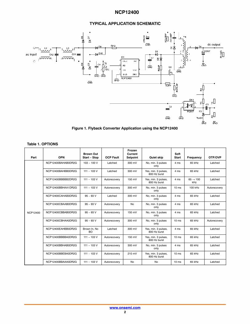
TYPICAL APPLICATION SCHEMATIC
Figure 1. Flyback Converter Application using the NCP12400
Table 1. OPTIONS
Part OPNBrown OutStart − Stop OCP Fault
FrozenCurrentSetpoint Quiet skip
SoftStart Frequency OTP/OVP
NCP12400
NCP12400BAHAB0DR2G 103 − 100 V Latched 300 mV No, min. 3 pulsesonly
4 ms 65 kHz Latched
NCP12400BAHBB0DR2G 111 − 103 V Latched 300 mV Yes, min. 3 pulses,800 Hz burst
4 ms 65 kHz Latched
NCP12400BBBBB2DR2G 111 − 103 V Autorecovery 150 mV Yes, min. 3 pulses,800 Hz burst
4 ms 65 → 100kHz
Latched
NCP12400BBHAA1DR2G 111 − 103 V Autorecovery 300 mV No, min. 3 pulsesonly
10 ms 100 kHz Autorecovery
NCP12400CAHAB0DR2G 95 − 93 V Latched 300 mV No, min. 3 pulsesonly
4 ms 65 kHz Latched
NCP12400CBAAB0DR2G 95 − 93 V Autorecovery No No, min. 3 pulsesonly
4 ms 65 kHz Latched
NCP12400CBBAB0DR2G 95 − 93 V Autorecovery 150 mV No, min. 3 pulsesonly
4 ms 65 kHz Latched
NCP12400CBHAA0DR2G 95 − 93 V Autorecovery 300 mV No, min. 3 pulsesonly
10 ms 65 kHz Autorecovery
NCP12400EAHBB0DR2G Brown In, NoBO
Latched 300 mV Yes, min. 3 pulses,800 Hz burst
4 ms 65 kHz Latched
NCP12400BBBBA0DR2G 111 − 103 V Autorecovery 150 mV Yes, min. 3 pulses,800 Hz burst
10 ms 65 kHz Latched
NCP12400BBHAB0DR2G 111 − 103 V Autorecovery 300 mV No, min. 3 pulsesonly
4 ms 65 kHz Latched
NCP12400BBEBA0DR2G 111 − 103 V Autorecovery 210 mV Yes, min. 3 pulses,800 Hz burst
10 ms 65 kHz Latched
NCP12400BBAAA0DR2G 111 − 103 V Autorecovery No No 10 ms 65 kHz Latched
NCP12400
www.onsemi.com3
Table 2. SPECIFIC DEVICE CODE KEY
400 V W X Y Z f
Part BO OCP Fault Frozen CurrentSetpoint
Quiet Skip Soft Start Frequency
A − 229−211 VB − 111−103 VC − 95−93 VD − No BO
E − Brown In, no BO
A − LatchedB − Autorecovery
A −NoB − 150 mVC − 170 mVD − 190 mVE − 210 mVF − 230 mVG − 250 mVH − 300 mV
A − No, min. 3pulses
B − Yes, min. 3pulses,
800 Hz burst
A − 10 msB − 4 ms
0 − 65 kHz1 − 100 kHz
2 − 65 → 100 kHz
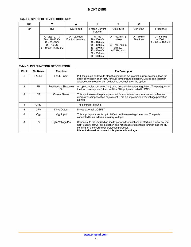
Table 3. PIN FUNCTION DESCRIPTION
Pin # Pin Name Function Pin Description
1 FAULT FAULT Input Pull the pin up or down to stop the controller. An internal current source allows the direct connection of an NTC for over temperature detection. Device can restart in autorecovery mode or can be latched depending on the option.
2 FB Feedback + ShutdownPin
An optocoupler connected to ground controls the output regulation. The part goes to the low consumption Off mode if the FB input pin is pulled to GND.
3 CS Current Sense This input senses the primary current for current−mode operation, and offers an overpower compensation adjustment. This pin implements over voltage protection as well.
4 GND The controller ground.
5 DRV Drive Output Drives external MOSFET.
6 VCC VCC Input This supply pin accepts up to 28 Vdc, with overvoltage detection. The pin is connected to an external auxiliary voltage.
8 HV High−Voltage Pin Connects to the rectified ac line to perform the functions of start−up current source, Self−Supply, brown−out detection and X2 capacitor discharge function and the HV sensing for the overpower protection purposes. It is not allowed to connect this pin to a dc voltage.
NCP12400
www.onsemi.com4
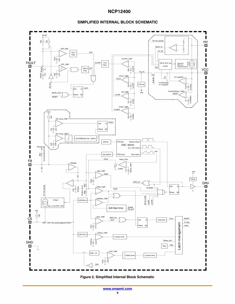
SIMPLIFIED INTERNAL BLOCK SCHEMATIC
Figure 2. Simplified Internal Block Schematic
freq folback
jittering
Vsk
ip
Skip _CMP
SkipB
Vra
mp
_of
fse
t
1.4
V4uMho
Ramp_OTACSref
Div
isio
nra
tio
4
Inte
rnal
resi
tanc
e40
k
Soft Start timer
Reset
QSet
Qb
Clamp
Fault timer
TSD
Lat
chm
anag
emen
t
FB
CS
DRV
GND
VCC
FaultIlimit_CMP
Rfb
2R
fb3
Vil
im
0.7
V
Fa
ultB
Lat
chB
PWM_CMP
SoftStart_CMPLEB 250 ns
LEB 120 nsCSstop_CMP
VC
Ss
top
1.0
5V
TSD
Latch
Enable
RESET
SS_end
Ilimit
Vfb(reg)
MAX_ton
MAX_ton
Bro
wn
_Ou
tB
Brown_Out
Reset
QSet
Qb
PWM
IC stop
V to I
Iopc = 0.5u*(Vhv −125)
Vfb
(opc
)
2.6V
Von
Off_mode_CMP1
ICstart
FBbuffer
Vh
vD
Csa
mp
le
2.2
V
VCC
UVLO_CMP
Vc
cOF
F
9.5
V
FAULT VccOVP
OTP
Vo
tp
0.4
V
Vo
vp
2.5V
OTP_CMP
OVP_CMP
Vcl
am
p
1.2
V
Rc
lam
p
1k
HVBrown_In
VccOVP_CMP
Vc
cOV
P
26V
Intc
Vdd
Intc
SS
_en
d
Set Q
Rese t Qb
Latch
Brown_Out
RESET
OVPAC_Off
UVLO
VCC
5uA
Vcc_Int
IC stopB
Vhv DC sample
OM & X2 & Vcc
Vdd reg
Vdd
Vcc regulator
PowerOnReset _CMP
Vc
c(re
g)
Vc
cRE
SE
T
10
.8V
7V
control
8m
A
Dual HVstart−upcurrent source
ICst
art
B
TSD
RESET
Vfb < 1.64 V fix current setpoint 210mV
X 2 discharge11 V regulator
ON_CMP
STOP_CMP
Vcc
ON
Vc
cMIN
12
V10
.5V
VccON
VccMIN
GoToOffMode timer 500ms
Set Q
Reset Qb
0.6V
Vo
ff
Off_mode_CMP2
FM input
OSC 65kHz
PFM input
Square output
Saw output
ton_max output
3. 0V
Vdd
1uA
4 events timer
LEB 1 usOVP_CMP
Vo
vp
1.0
5V
DRV
4 events timer600ns timer
55 usFilter
300 usFilter
10 usFilter
Rfb
1
NCP12400
www.onsemi.com5
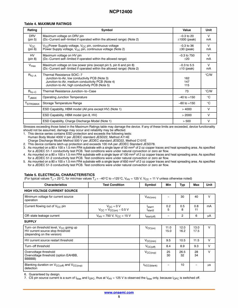
Table 4. MAXIMUM RATINGS
Rating Symbol Value Unit
DRV(pin 5)
Maximum voltage on DRV pin(Dc−Current self−limited if operated within the allowed range) (Note 2)
–0.3 to 20±1000 (peak)
VmA
VCC(pin 6)
VCCPower Supply voltage, VCC pin, continuous voltagePower Supply voltage, VCC pin, continuous voltage (Note 2)
–0.3 to 36±30 (peak)
VmA
HV(pin 8)
Maximum voltage on HV pin(Dc−Current self−limited if operated within the allowed range)
–0.3 to 750±20
VmA
Vmax Maximum voltage on low power pins (except pin 5, pin 6 and pin 8)(Dc−Current self−limited if operated within the allowed range) (Note 2)
–0.3 to 5.5±10 (peak)
VmA
R�J−A Thermal Resistance SOIC−7Junction-to-Air, low conductivity PCB (Note 3)Junction-to-Air, medium conductivity PCB (Note 4)Junction-to-Air, high conductivity PCB (Note 5)
162147115
°C/W
R�J−C Thermal Resistance Junction−to−Case 73 °C/W
TJMAX Operating Junction Temperature −40 to +150 °C
TSTRGMAX Storage Temperature Range −60 to +150 °C
ESD Capability, HBM model (All pins except HV) (Note 1) > 4000 V
ESD Capability, HBM model (pin 8, HV) > 2000 V
ESD Capability, Charge Discharge Model (Note 1) > 500 V
Stresses exceeding those listed in the Maximum Ratings table may damage the device. If any of these limits are exceeded, device functionalityshould not be assumed, damage may occur and reliability may be affected.1. This device series contains ESD protection and exceeds the following tests:
Human Body Model 4000 V per JEDEC standard JESD22, Method A114ECharge Discharge Model Method 500 V per JEDEC standard JESD22, Method C101E
2. This device contains latch-up protection and exceeds 100 mA per JEDEC Standard JESD78.3. As mounted on a 80 x 100 x 1.5 mm FR4 substrate with a single layer of 50 mm2 of 2 oz copper traces and heat spreading area. As specified
for a JEDEC 51-1 conductivity test PCB. Test conditions were under natural convection or zero air flow.4. As mounted on a 80 x 100 x 1.5 mm FR4 substrate with a single layer of 100 mm2 of 2 oz copper traces and heat spreading area. As specified
for a JEDEC 51-2 conductivity test PCB. Test conditions were under natural convection or zero air flow.5. As mounted on a 80 x 100 x 1.5 mm FR4 substrate with a single layer of 650 mm2 of 2 oz copper traces and heat spreading area. As specified
for a JEDEC 51-3 conductivity test PCB. Test conditions were under natural convection or zero air flow.
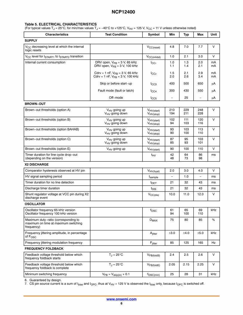
Table 5. ELECTRICAL CHARACTERISTICS (For typical values TJ = 25°C, for min/max values TJ = −40°C to +125°C, VHV = 125 V, VCC = 11 V unless otherwise noted)
Characteristics Test Condition Symbol Min Typ Max Unit
HIGH VOLTAGE CURRENT SOURCE
Minimum voltage for current sourceoperation
VHV(min) − 30 40 V
Current flowing out of VCC pin VCC = 0 VVCC = VCC(on) − 0.5 V
Istart1Istart2
0.25
0.58
0.811
mA
Off−state leakage current VHV = 750 V, VCC = 15 V Istart(off) − 2 6 �A
SUPPLY
Turn−on threshold level, VCC going upHV current source stop threshold(depending on the version)
VCC(on) 11.015.0
12.016.2
13.017.5
V
HV current source restart threshold VCC(min) 9.5 10.5 11.5 V
Turn−off threshold VCC(off) 8.4 8.9 9.3 V
Overvoltage thresholdOvervoltage threshold (option EAHBB,BBBBB)
VCC(ovp) 2530
26.532
2834
V
Blanking duration on VCC(off) and VCC(ovp)detection
tVCC(blank) − 10 − �s
6. Guaranteed by design.7. CS pin source current is a sum of Ibias and IOPC, thus at VHV = 125 V is observed the Ibias only, because IOPC is switched off.
NCP12400
www.onsemi.com6
Table 5. ELECTRICAL CHARACTERISTICS (For typical values TJ = 25°C, for min/max values TJ = −40°C to +125°C, VHV = 125 V, VCC = 11 V unless otherwise noted)
Characteristics UnitMaxTypMinSymbolTest Condition
SUPPLY
VCC decreasing level at which the internallogic resets
VCC(reset) 4.8 7.0 7.7 V
VCC level for ISTART1 to ISTART2 transition VCC(inhibit) 1.0 2.1 3.0 V
Internal current consumption DRV open, VFB = 3 V, 65 kHzDRV open, VFB = 3 V, 100 kHz
Cdrv = 1 nF, VFB = 3 V, 65 kHzCdrv = 1 nF, VFB = 3 V, 100 kHz
Skip or before start−up
Fault mode (fault or latch)
Off−mode
ICC1
ICC2
ICC3
ICC4
ICC5
1.01.1
1.52.0
400
300
−
1.31.4
2.12.6
500
430
25
2.02.1
2.93.4
650
550
−
mAmA
mAmA
�A
�A
�A
BROWN−OUT
Brown−out thresholds (option A) VHV going upVHV going down
VHV(start)VHV(stop)
210194
229211
248228
V
Brown−out thresholds (option B) VHV going upVHV going down
VHV(start)VHV(stop)
10294
111103
120116
V
Brown−out thresholds (option BAHAB) VHV going upVHV going down
VHV(start)VHV(stop)
9390
103100
113110
V
Brown−out thresholds (option C) VHV going upVHV going down
VHV(start)VHV(stop)
8785
9593
103101
V
Brown−out thresholds (option E) VHV going up VHV(start) 90 100 110 V
Timer duration for line cycle drop−out(depending on the version)
tHV 4248
6473
8698
ms
X2 DISCHARGE
Comparator hysteresis observed at HV pin VHV(hyst) 2.0 3.0 4.0 V
HV signal sampling period tsample − 1.0 − ms
Timer duration for no line detection tDET 21 32 43 ms
Discharge timer duration tDIS 21 32 43 ms
Shunt regulator voltage at VCC pin during X2discharge event
VCC(dis) 10.0 11.0 12.0 V
OSCILLATOR
Oscillator frequency 65 kHz versionOscillator frequency 100 kHz version
fOSC 6194
65100
69110
kHz
Maximum duty−ratio (corresponding tomaximum on time at maximum switchingfrequency)
DMAX 75 80 85 %
Frequency jittering amplitude, in percentageof FOSC
Ajitter ±3.0 ±4.0 ±5.0 kHz
Frequency jittering modulation frequency Fjitter 85 125 165 Hz
FREQUENCY FOLDBACK
Feedback voltage threshold below whichfrequency foldback starts
TJ = 25°C VFB(foldS) 2.4 2.5 2.6 V
Feedback voltage threshold below whichfrequency foldback is complete
TJ = 25°C VFB(foldE) 2.05 2.15 2.25 V
Minimum switching frequency VFB = Vskip(in) + 0.1 fOSC(min) 25 28 31 kHz
6. Guaranteed by design.7. CS pin source current is a sum of Ibias and IOPC, thus at VHV = 125 V is observed the Ibias only, because IOPC is switched off.
NCP12400
www.onsemi.com7
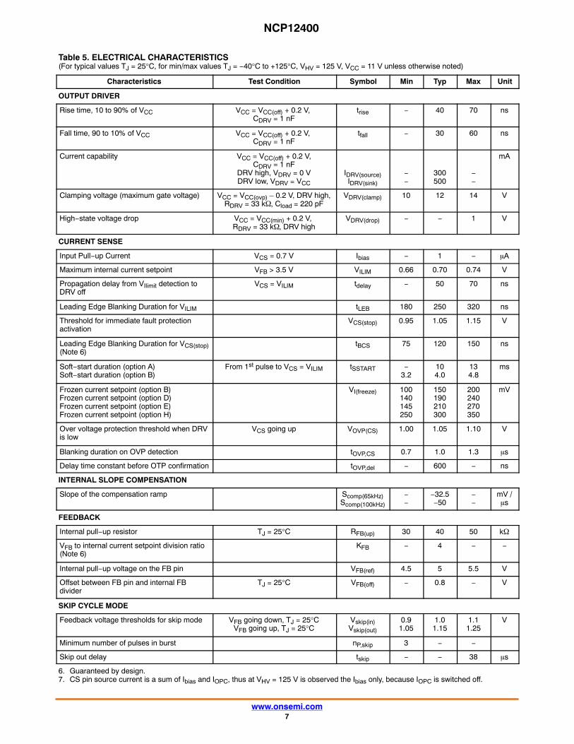
Table 5. ELECTRICAL CHARACTERISTICS (For typical values TJ = 25°C, for min/max values TJ = −40°C to +125°C, VHV = 125 V, VCC = 11 V unless otherwise noted)
Characteristics UnitMaxTypMinSymbolTest Condition
OUTPUT DRIVER
Rise time, 10 to 90% of VCC VCC = VCC(off) + 0.2 V, CDRV = 1 nF
trise − 40 70 ns
Fall time, 90 to 10% of VCC VCC = VCC(off) + 0.2 V, CDRV = 1 nF
tfall − 30 60 ns
Current capability VCC = VCC(off) + 0.2 V,CDRV = 1 nF
DRV high, VDRV = 0 VDRV low, VDRV = VCC
IDRV(source)IDRV(sink)
−−
300500
−−
mA
Clamping voltage (maximum gate voltage) VCC = VCC(ovp) – 0.2 V, DRV high,RDRV = 33 k�, Cload = 220 pF
VDRV(clamp) 10 12 14 V
High−state voltage drop VCC = VCC(min) + 0.2 V, RDRV = 33 k�, DRV high
VDRV(drop) − − 1 V
CURRENT SENSE
Input Pull−up Current VCS = 0.7 V Ibias − 1 − �A
Maximum internal current setpoint VFB > 3.5 V VILIM 0.66 0.70 0.74 V
Propagation delay from VIlimit detection toDRV off
VCS = VILIM tdelay − 50 70 ns
Leading Edge Blanking Duration for VILIM tLEB 180 250 320 ns
Threshold for immediate fault protectionactivation
VCS(stop) 0.95 1.05 1.15 V
Leading Edge Blanking Duration for VCS(stop)(Note 6)
tBCS 75 120 150 ns
Soft−start duration (option A)Soft−start duration (option B)
From 1st pulse to VCS = VILIM tSSTART −3.2
104.0
134.8
ms
Frozen current setpoint (option B)Frozen current setpoint (option D)Frozen current setpoint (option E)Frozen current setpoint (option H)
VI(freeze) 100140145250
150190210300
200240270350
mV
Over voltage protection threshold when DRVis low
VCS going up VOVP(CS) 1.00 1.05 1.10 V
Blanking duration on OVP detection tOVP,CS 0.7 1.0 1.3 �s
Delay time constant before OTP confirmation tOVP,del − 600 − ns
INTERNAL SLOPE COMPENSATION
Slope of the compensation ramp Scomp(65kHz)Scomp(100kHz)
−−
−32.5−50
−−
mV /�s
FEEDBACK
Internal pull−up resistor TJ = 25°C RFB(up) 30 40 50 k�
VFB to internal current setpoint division ratio(Note 6)
KFB − 4 − −
Internal pull−up voltage on the FB pin VFB(ref) 4.5 5 5.5 V
Offset between FB pin and internal FBdivider
TJ = 25°C VFB(off) − 0.8 − V
SKIP CYCLE MODE
Feedback voltage thresholds for skip mode VFB going down, TJ = 25°CVFB going up, TJ = 25°C
Vskip(in)Vskip(out)
0.91.05
1.01.15
1.11.25
V
Minimum number of pulses in burst nP,skip 3 − −
Skip out delay tskip − − 38 �s
6. Guaranteed by design.7. CS pin source current is a sum of Ibias and IOPC, thus at VHV = 125 V is observed the Ibias only, because IOPC is switched off.
NCP12400
www.onsemi.com8
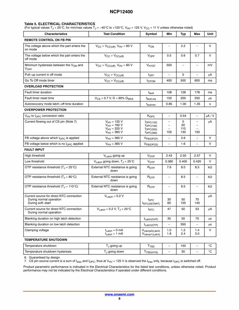
Table 5. ELECTRICAL CHARACTERISTICS (For typical values TJ = 25°C, for min/max values TJ = −40°C to +125°C, VHV = 125 V, VCC = 11 V unless otherwise noted)
Characteristics UnitMaxTypMinSymbolTest Condition
REMOTE CONTROL ON FB PIN
The voltage above which the part enters theon mode
VCC > VCC(off), VHV = 60 V VON − 2.2 − V
The voltage below which the part enters theoff mode
VCC > VCC(off) VOFF 0.5 0.6 0.7 V
Minimum hysteresis between the VON andVOFF
VCC > VCC(off), VHV = 60 V VHYST 500 − − mV
Pull−up current in off mode VCC > VCC(off) IOFF − 5 − �A
Go To Off mode timer VCC > VCC(off) tGTOM 400 500 600 ms
OVERLOAD PROTECTION
Fault timer duration tfault 108 128 178 ms
Fault timer reset time VCS < 0.7 V, D < 90% DMAX tfault,res 150 200 250 �s
Autorecovery mode latch−off time duration tautorec 0.85 1.00 1.35 s
OVERPOWER PROTECTION
VHV to IOPC conversion ratio KOPC − 0.54 − �A / V
Current flowing out of CS pin (Note 7) VHV = 125 VVHV = 162 VVHV = 325 VVHV = 365 V
IOPC(125)IOPC(162)IOPC(325)IOPC(365)
−−−
105
020110130
−−−
150
�A
FB voltage above which IOPC is applied VHV = 365 V VFB(OPCF) − 2.6 − V
FB voltage below which is no IOPC applied VHV = 365 V VFB(OPCE) − 1.6 − V
FAULT INPUT
High threshold VLatch going up VOVP 2.43 2.50 2.57 V
Low threshold VLatch going down, TJ = 25°C VOTP 0.380 0.400 0.420 V
OTP resistance threshold (TJ = 25°C) External NTC resistance is goingdown
ROTP 7.6 8.0 8.5 k�
OTP resistance threshold (TJ = 80°C) External NTC resistance is goingdown
ROTP − 8.5 − k�
OTP resistance threshold (TJ = 110°C) External NTC resistance is goingdown
ROTP − 9.5 − k�
Current source for direct NTC connectionDuring normal operationDuring soft−start
VLatch = 0.2 VINTC
INTC(SSTART)
3060
50100
70140
�A
Current source for direct NTC connectionDuring normal operation
VLatch = 0.2 V, TJ = 25°C INTC 47 50 53 �A
Blanking duration on high latch detection tLatch(OVP) 35 50 70 �s
Blanking duration on low latch detection tLatch(OTP) − 350 − �s
Clamping voltage ILatch = 0 mAILatch = 1 mA
Vclamp0(Latch)Vclamp1(Latch)
1.01.8
1.22.4
1.43.0
V
TEMPERATURE SHUTDOWN
Temperature shutdown TJ going up TTSD − 150 − °C
Temperature shutdown hysteresis TJ going down TTSD(HYS) − 30 − °C
6. Guaranteed by design.7. CS pin source current is a sum of Ibias and IOPC, thus at VHV = 125 V is observed the Ibias only, because IOPC is switched off.
Product parametric performance is indicated in the Electrical Characteristics for the listed test conditions, unless otherwise noted. Productperformance may not be indicated by the Electrical Characteristics if operated under different conditions.
NCP12400
www.onsemi.com9
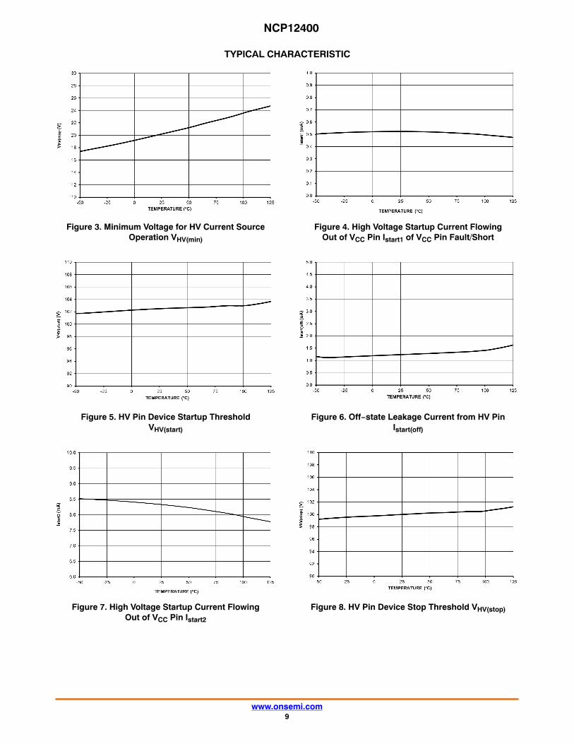
TYPICAL CHARACTERISTIC
Figure 3. Minimum Voltage for HV Current SourceOperation VHV(min)
Figure 4. High Voltage Startup Current FlowingOut of VCC Pin Istart1 of VCC Pin Fault/Short
Figure 5. HV Pin Device Startup ThresholdVHV(start)
Figure 6. Off−state Leakage Current from HV PinIstart(off)
Figure 7. High Voltage Startup Current FlowingOut of VCC Pin Istart2
Figure 8. HV Pin Device Stop Threshold VHV(stop)
NCP12400
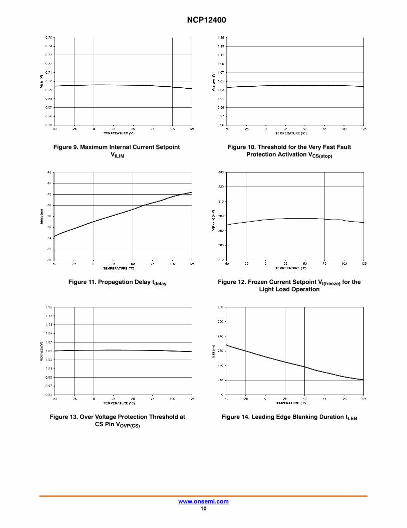
www.onsemi.com10
Figure 9. Maximum Internal Current Setpoint VILIM
Figure 10. Threshold for the Very Fast FaultProtection Activation VCS(stop)
Figure 11. Propagation Delay tdelay Figure 12. Frozen Current Setpoint VI(freeze) for theLight Load Operation
Figure 13. Over Voltage Protection Threshold atCS Pin VOVP(CS)
Figure 14. Leading Edge Blanking Duration tLEB
NCP12400
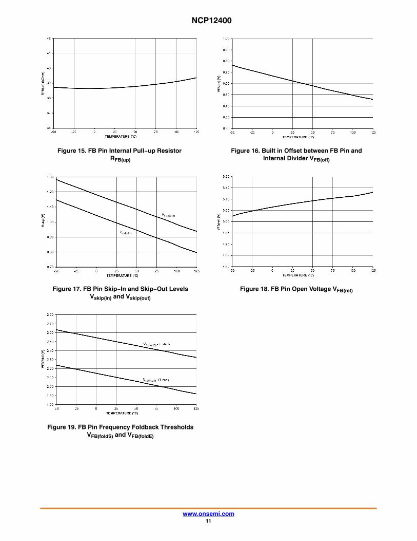
www.onsemi.com11
Figure 15. FB Pin Internal Pull−up Resistor RFB(up)
Figure 16. Built in Offset between FB Pin andInternal Divider VFB(off)
Figure 17. FB Pin Skip−In and Skip−Out LevelsVskip(in) and Vskip(out)
Figure 18. FB Pin Open Voltage VFB(ref)
Figure 19. FB Pin Frequency Foldback ThresholdsVFB(foldS) and VFB(foldE)
NCP12400
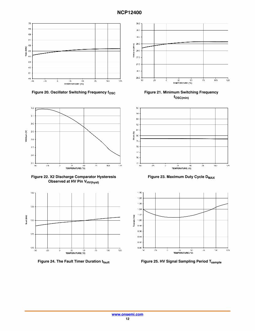
www.onsemi.com12
Figure 20. Oscillator Switching Frequency fOSC Figure 21. Minimum Switching FrequencyfOSC(min)
Figure 22. X2 Discharge Comparator HysteresisObserved at HV Pin VHV(hyst)
Figure 23. Maximum Duty Cycle DMAX
Figure 24. The Fault Timer Duration tfault Figure 25. HV Signal Sampling Period Tsample
NCP12400
www.onsemi.com13
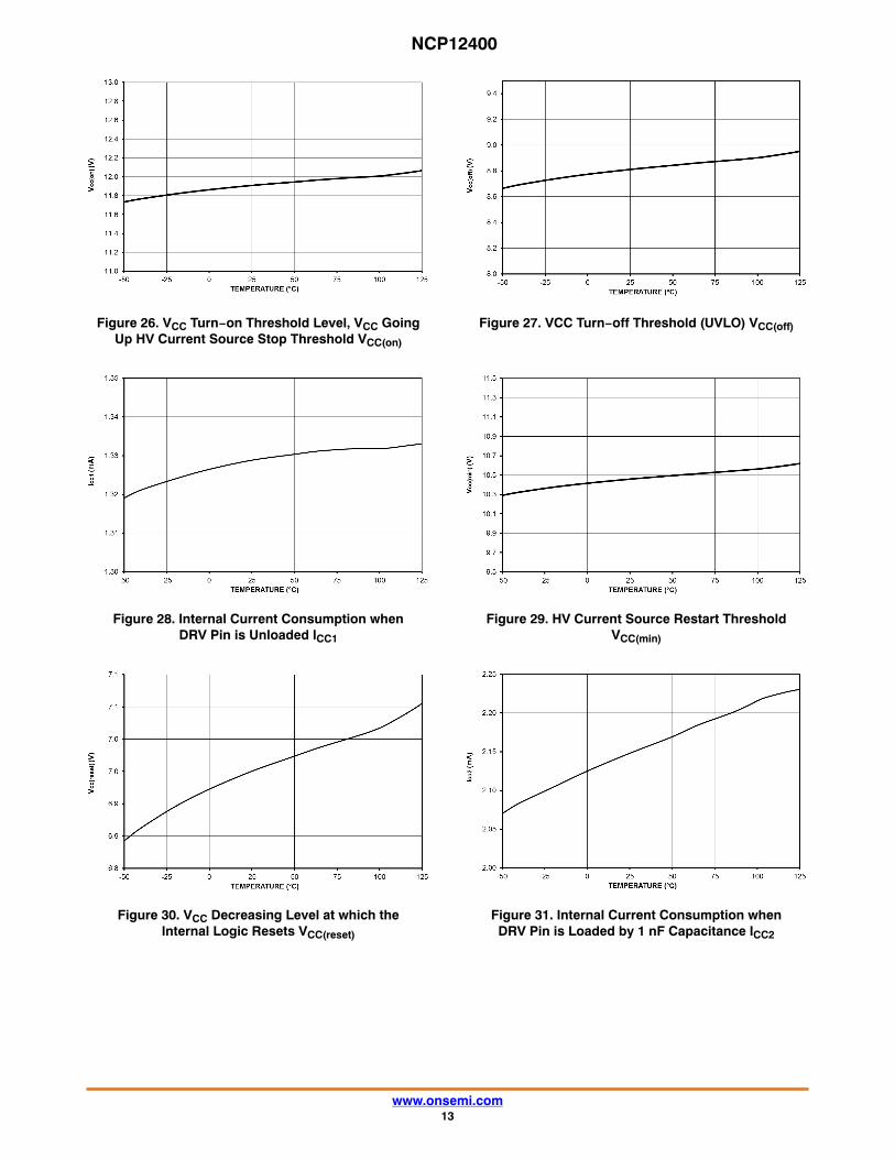
Figure 26. VCC Turn−on Threshold Level, VCC GoingUp HV Current Source Stop Threshold VCC(on)
Figure 27. VCC Turn−off Threshold (UVLO) VCC(off)
Figure 28. Internal Current Consumption whenDRV Pin is Unloaded ICC1
Figure 29. HV Current Source Restart ThresholdVCC(min)
Figure 30. VCC Decreasing Level at which theInternal Logic Resets VCC(reset)
Figure 31. Internal Current Consumption whenDRV Pin is Loaded by 1 nF Capacitance ICC2
NCP12400
www.onsemi.com14
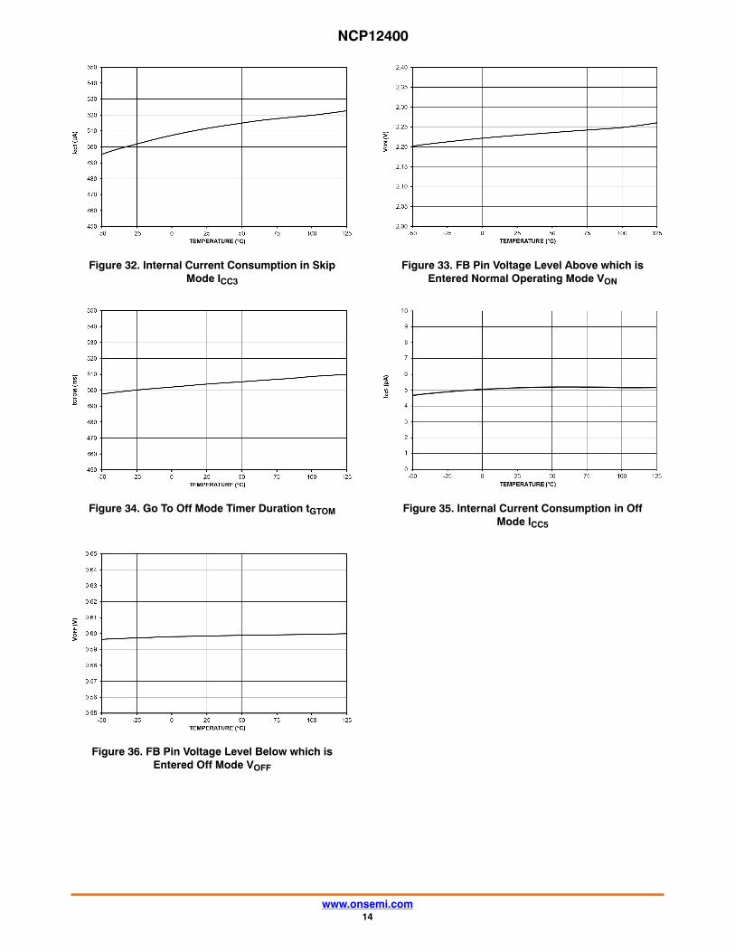
Figure 32. Internal Current Consumption in SkipMode ICC3
Figure 33. FB Pin Voltage Level Above which isEntered Normal Operating Mode VON
Figure 34. Go To Off Mode Timer Duration tGTOM Figure 35. Internal Current Consumption in OffMode ICC5
Figure 36. FB Pin Voltage Level Below which isEntered Off Mode VOFF
NCP12400
www.onsemi.com15
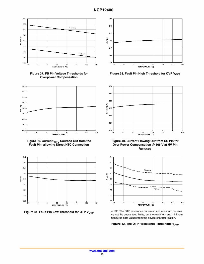
Figure 37. FB Pin Voltage Thresholds forOverpower Compensation
Figure 38. Fault Pin High Threshold for OVP VOVP
Figure 39. Current INTC Sourced Out from theFault Pin, allowing Direct NTC Connection
Figure 40. Current Flowing Out from CS Pin forOver Power Compensation @ 365 V at HV Pin
IOPC(365)
Figure 41. Fault Pin Low Threshold for OTP VOTP
Figure 42. The OTP Resistance Threshold ROTP
NOTE: The OTP resistance maximum and minimum coursesare not the guaranteed limits, but the maximum and minimummeasured data values from the device characterization.
NCP12400
www.onsemi.com16
APPLICATION INFORMATION
Functional DescriptionThe NCP12400 includes all necessary features to build a
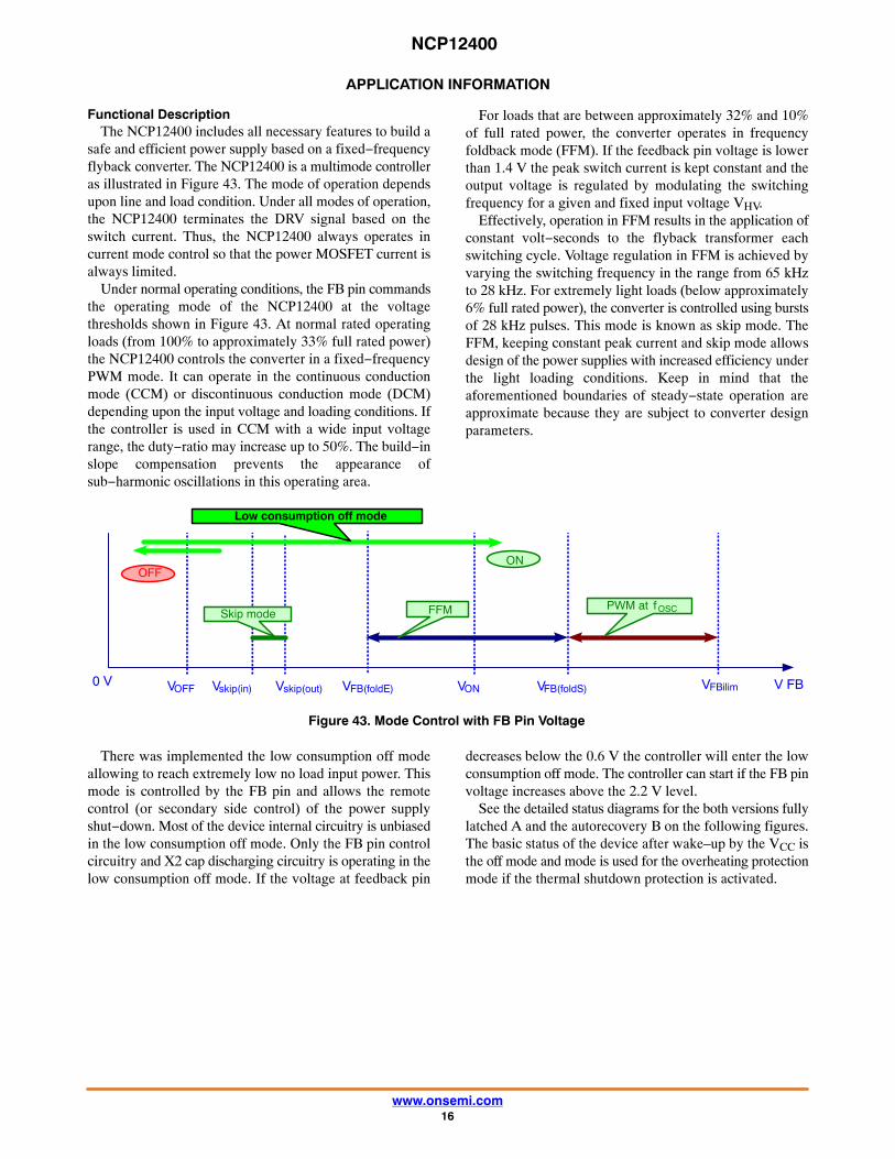
safe and efficient power supply based on a fixed−frequencyflyback converter. The NCP12400 is a multimode controlleras illustrated in Figure 43. The mode of operation dependsupon line and load condition. Under all modes of operation,the NCP12400 terminates the DRV signal based on theswitch current. Thus, the NCP12400 always operates incurrent mode control so that the power MOSFET current isalways limited.
Under normal operating conditions, the FB pin commandsthe operating mode of the NCP12400 at the voltagethresholds shown in Figure 43. At normal rated operatingloads (from 100% to approximately 33% full rated power)the NCP12400 controls the converter in a fixed−frequencyPWM mode. It can operate in the continuous conductionmode (CCM) or discontinuous conduction mode (DCM)depending upon the input voltage and loading conditions. Ifthe controller is used in CCM with a wide input voltagerange, the duty−ratio may increase up to 50%. The build−inslope compensation prevents the appearance ofsub−harmonic oscillations in this operating area.
For loads that are between approximately 32% and 10%of full rated power, the converter operates in frequencyfoldback mode (FFM). If the feedback pin voltage is lowerthan 1.4 V the peak switch current is kept constant and theoutput voltage is regulated by modulating the switchingfrequency for a given and fixed input voltage VHV.
Effectively, operation in FFM results in the application ofconstant volt−seconds to the flyback transformer eachswitching cycle. Voltage regulation in FFM is achieved byvarying the switching frequency in the range from 65 kHzto 28 kHz. For extremely light loads (below approximately6% full rated power), the converter is controlled using burstsof 28 kHz pulses. This mode is known as skip mode. TheFFM, keeping constant peak current and skip mode allowsdesign of the power supplies with increased efficiency underthe light loading conditions. Keep in mind that theaforementioned boundaries of steady−state operation areapproximate because they are subject to converter designparameters.
Figure 43. Mode Control with FB Pin Voltage
V FBVFBilimVON VFB(foldS)VFB(foldE)Vskip(out)Vskip(in)VOFF
FFM PWM at f OSCSkip mode
0 V
Low consumption off mode
OFFON
There was implemented the low consumption off modeallowing to reach extremely low no load input power. Thismode is controlled by the FB pin and allows the remotecontrol (or secondary side control) of the power supplyshut−down. Most of the device internal circuitry is unbiasedin the low consumption off mode. Only the FB pin controlcircuitry and X2 cap discharging circuitry is operating in thelow consumption off mode. If the voltage at feedback pin
decreases below the 0.6 V the controller will enter the lowconsumption off mode. The controller can start if the FB pinvoltage increases above the 2.2 V level.
See the detailed status diagrams for the both versions fullylatched A and the autorecovery B on the following figures.The basic status of the device after wake–up by the VCC isthe off mode and mode is used for the overheating protectionmode if the thermal shutdown protection is activated.
NCP12400
www.onsemi.com17
Figure 44. Operating Status Diagram of the Device
Extra Low
Consum
ption
Pow
er On
Reset
Latch=
0A
utoRec
=0
(VF
B <V
OF
F )*GT
OM
timer
*(VC
C >V
CC
off )
Off M
ode
Latch=
XA
utoRec
=X
AutoR
ec
Latch
Latch=
1
Stop
Reset
Latch=
0A
utoRec
=0
Autorecovery
Latch
AutoR
ec=
1
VC
C <V
CC
reset
BO
+T
SD
BO
+T
SD
(VC
C >V
CC
on )*BO
Soft
Start
Running
Skip
mode S
kip in
SS
end
BO
BO
BO
VC
Sstop
Efficient operating m
ode
Dynam
ic Self−
Supply
Dynam
ic Self−
Supply
(if not enoughgh auxiliary voltage ispresent)
VC
C
fault
VC
C <V
CC
off
VC
C >V
CC
off
X2
capD
ischarge
Latch=
0A
utoRec
=0
No A
C
VH
V >V
HV
(min
)
Check
Latch=
XA
utoRec
=X
Latch*A
utoRec
VF
B >V
ON
Skip in
Skip outdelay
AutorecoveryC
ondition=
(VC
Sstop
*4clk
) + (
VILIM
+M
axDC
)*tfault+
(VC
C <V
CC
off )*tVC
C(blank
)
LatchCondition
=O
VP
+O
TP
+V
CC
ovp*tV
CC
(blank)
Co
nd
ition
s for A
uto
recovery versio
n (B
)
LatchCondition =
OV
P+
OT
P+
VC
Covp *tV
CC
(blank)
+ (V
CS
stop*4
clk) +
(V
ILIM+
MaxD
C)*tfault
Co
nd
ition
s for L
atched
version
(A)
LatchCondition
VC
C <V
CC
reset
NCP12400
www.onsemi.com18
Figure 45. VCC Management Timing Diagram
time
VC
C
HV
currentsource=
Istart1
VC
C(on)
VC
C(m
in)
VC
C(inhibit)
VC
C(off)
VC
C(dis)
X2
discharge
Before start
Lo
w co
nsu
mp
tion
off m
od
eN
ormal m
odeO
verloadF
ault mode
tauto
rec
HV
currentsource=
Istart2
UV
LO level
VC
C(off)
is trigged before OC
P tim
er elapsed
The information about the fault (permanent Latch orAutorecovery) is kept during the low consumption off modedue the safety reason. The reason is not to allow unlatch thedevice by the remote control being in off mode.
Start−up of the ControllerAt start−up, the current source turns on when the voltage
on the HV pin is higher than VHV(min), and turns off whenVCC reaches VCC(on), then turns on again when VCC reaches
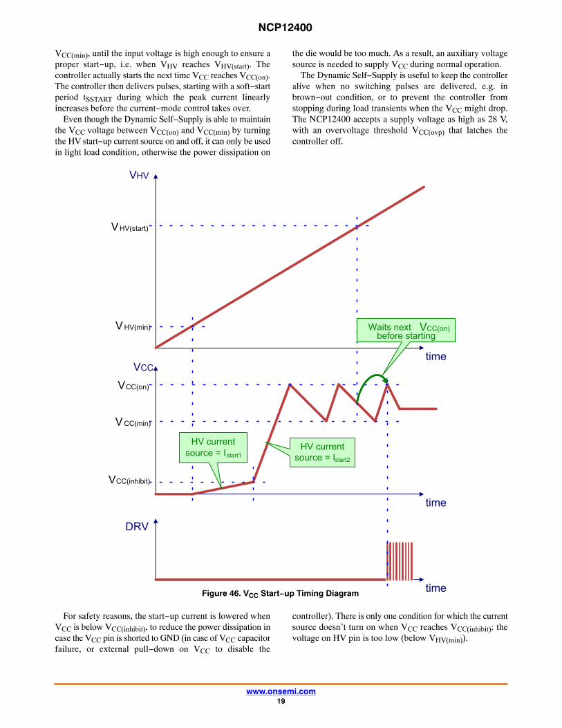
NCP12400
www.onsemi.com19
VCC(min), until the input voltage is high enough to ensure aproper start−up, i.e. when VHV reaches VHV(start). Thecontroller actually starts the next time VCC reaches VCC(on).The controller then delivers pulses, starting with a soft−startperiod tSSTART during which the peak current linearlyincreases before the current−mode control takes over.
Even though the Dynamic Self−Supply is able to maintainthe VCC voltage between VCC(on) and VCC(min) by turningthe HV start−up current source on and off, it can only be usedin light load condition, otherwise the power dissipation on
the die would be too much. As a result, an auxiliary voltagesource is needed to supply VCC during normal operation.
The Dynamic Self−Supply is useful to keep the controlleralive when no switching pulses are delivered, e.g. inbrown−out condition, or to prevent the controller fromstopping during load transients when the VCC might drop.The NCP12400 accepts a supply voltage as high as 28 V,with an overvoltage threshold VCC(ovp) that latches thecontroller off.
Figure 46. VCC Start−up Timing Diagram
time
VHV
time
VCC
time
DRV
VHV(start)
V HV(min)
VCC(on)
V CC(min)
HV current
source = Istart1
HV current
source = Istart2
Waits next VCC(on)before starting
VCC(inhibit)
For safety reasons, the start−up current is lowered whenVCC is below VCC(inhibit), to reduce the power dissipation incase the VCC pin is shorted to GND (in case of VCC capacitorfailure, or external pull−down on VCC to disable the
controller). There is only one condition for which the currentsource doesn’t turn on when VCC reaches VCC(inhibit): thevoltage on HV pin is too low (below VHV(min)).
NCP12400
www.onsemi.com20
Figure 47. Latch After the Preshort
time
VHV
time
VCC
time
DRV
VHV(start)
VHV(min)
VCC(on)
VCC(min)
HV currentsource = Istart1
HV currentsource = Istart2
Device starts atVCC(on) event
VCC(inhibit)
VCC(off)
UVLO level VCC (off )
is trigged before OCP timer elapsed
Device stops thanksto pre−short protection
HV Sensing of Rectified AC VoltageThe NCP12400 features on its HV pin a true ac line
monitoring circuitry. It includes a minimum start−upthreshold and an autorecovery brown−out protection; bothof them independent of the ripple on the input voltage. It isallowed only to work with an unfiltered, rectified ac input toensure the X2 capacitor discharge function as well, which isdescribed in following. The brown−out protection
thresholds are fixed, but they are designed to fit most of thestandard ac−dc conversion applications.
When the input voltage goes below VHV(stop), abrown−out condition is detected, and the controller stops.The HV current source maintains VCC between VCC(on) andVCC(min) levels until the input voltage is back aboveVHV(start).
NCP12400
www.onsemi.com21
Figure 48. Ac Line Drop−out Timing Diagram
time
HV stop
time
VCC
time
DRV
VCC(on)
VCC(min)
Waits nextVccON before
starting
Brown−outdetected
time
VHVHV timer elapsed
VHV (start )
VHV(stop)
Brown−outconditionresets the
Internal Latch
tHV
When VHV crosses the VHV(start) threshold, the controllercan start immediately. When it crosses VHV(stop), it triggersa timer of duration tHV, this ensures that the controllerdoesn’t stop in case of line cycle drop−out.
When VHV crosses the VHV(start) threshold, the controllerstarts when the VCC crosses the next VCC(on) event. Whenit crosses VHV(stop), it triggers a timer of duration tHV, thisensures that the controller doesn’t stop in case of line cycle
drop−out. The device restart after the ac line voltagedrop−out is protected to the parasitic restart initiated e.g. thespikes induced at HV pin immediately after the device isstopped by the residual energy in the EMI filter. The devicerestart is allowed only after the 1st watch dog signal event.The basic principle is shown at Figure 49 and detail of thedevice restart is shown at Figure 50.
NCP12400
www.onsemi.com22
Figure 49. Ac Line Drop−out Timing Diagram with the Parasitic Spike
time
HV stop
time
VCC
time
DRV
VCC(on)
VCC(min)
Waits nextVccON before
starting
time
VHVHV timer elapsed
VHV(start)
VHV(stop)
Brown−outconditionresets the
Internal Latch
tHV
Brown−outdetected
Spike induced byresidual energy in
EMI filter
NCP12400
www.onsemi.com23
Figure 50. Detailed Timing Diagram of the Device Restart after the Short ac Line Drop−out
time
VHV SAMPLE
ComparatorOutput
TSAMPLE
2 nd sample clockpulse after last
HV edge initiatesthe watch dog
signal
VHV (hyst )
Sample clock
Watch dogsignal
1st HV edgeresets the watch
dog and startsthe peak
detection of HVpin signal
2nd sample clockpulse after last
HV edge initiatesthe watch dog
signal
HV stop
DRV
tHV
Brown−outdetected
VHV(start )
VHV(stop )
time
VCC
VCC (on )
VCC(mini)
Device can restart after1st Watch dog signal
when HV signalcrosses V HV(start ) level
Device is stopped Device restarts
time
time
time
time
time
NCP12400
www.onsemi.com24
X2 Cap Discharge FeatureThe X2 capacitor discharging feature is offered by usage
of the NCP12400. This feature save approx. 16 mW –25 mW input power depending on the EMI filter X2capacitors volume and it saves the external componentscount as well. The discharge feature is ensured via thestart−up current source with a dedicated control circuitry forthis function. The X2 capacitors are being discharged bycurrent defined as Istart2 when this need is detected.
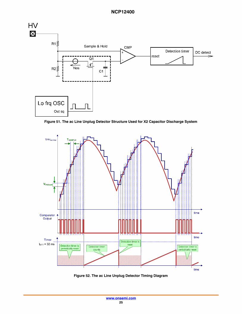
There is used a dedicated structure called ac line unplugdetector inside the X2 capacitor discharge control circuitry.See the Figure 51 for the block diagram for this structure andFigures 52, 53, 54 and 55 for the timing diagrams. The basicidea of ac line unplug detector lies in comparison of thedirect sample of the high voltage obtained via the highvoltage sensing structure with the delayed sample of the highvoltage. The delayed signal is created by the sample & holdstructure.
The comparator used for the comparison of these signalsis without hysteresis inside. The resolution between theslopes of the ac signal and dc signal is defined by thesampling time TSAMPLE and additional internal offset NOS.These parameters ensure the noise immunity as well. Theadditional offset is added to the picture of the sampled HVsignal and its analog sum is stored in the C1 storagecapacitor. If the voltage level of the HV sensing structureoutput crosses this level the comparator CMP output signalresets the detection timer and no dc signal is detected. Theadditional offset NOS can be measured as the VHV(hyst) onthe HV pin. If the comparator output produces pulses itmeans that the slope of input signal is higher than setresolution level and the slope is positive. If the comparatoroutput produces the low level it means that the slope of inputsignal is lower than set resolution level or the slope isnegative. There is used the detection timer which is reset byany edge of the comparator output. It means if no edgecomes before the timer elapses there is present only dc signalor signal with the small ac ripple at the HV pin. This type ofthe ac detector detects only the positive slope, which fulfilsthe requirements for the ac line presence detection.
In case of the dc signal presence on the high voltage input,the direct sample of the high voltage obtained via the highvoltage sensing structure and the delayed sample of the highvoltage are equivalent and the comparator produces the lowlevel signal during the presence of this signal. No edges arepresent at the output of the comparator, that’s why thedetection timer is not reset and dc detect signal appears.
The minimum detectable slope by this ac detector is givenby the ration between the maximum hysteresis observed atHV pin VHV(hyst),max and the sampling time:
Smin �
VHV(hyst),max
Tsample
(eq. 1)
Than it can be derived the relationship between theminimum detectable slope and the amplitude and frequencyof the sinusoidal input voltage:
Vmax �
VHV(hyst),max
2 � � � f � Tsample
�
5
2 � � � 35 � 1 � 10−3�
(eq. 2)� 22.7 V
The minimum detectable AC RMS voltage is 16 V atfrequency 35 Hz, if the maximum hysteresis is 5 V andsampling time is 1 ms.
The X2 capacitor discharge feature is available in anycontroller operation mode to ensure this safety feature. Thedetection timer is reused for the time limiting of thedischarge phase, to protect the device against overheating.The discharging process is cyclic and continues until the acline is detected again or the voltage across the X2 capacitoris lower than VHV(min). This feature ensures to dischargequite big X2 capacitors used in the input line filter to the safelevel. It is important to note that it is not allowed toconnect HV pin to any dc voltage due this feature. e.g.directly to bulk capacitor.
During the HV sensing or X2 cap discharging the VCC netis kept above the VCC(off) voltage by the Self−Supply in anymode of device operation to supply the control circuitry.During the discharge sequence is not allowed to start−up thedevice.
NCP12400
www.onsemi.com25
Figure 51. The ac Line Unplug Detector Structure Used for X2 Capacitor Discharge System
Figure 52. The ac Line Unplug Detector Timing Diagram
NCP12400
www.onsemi.com26
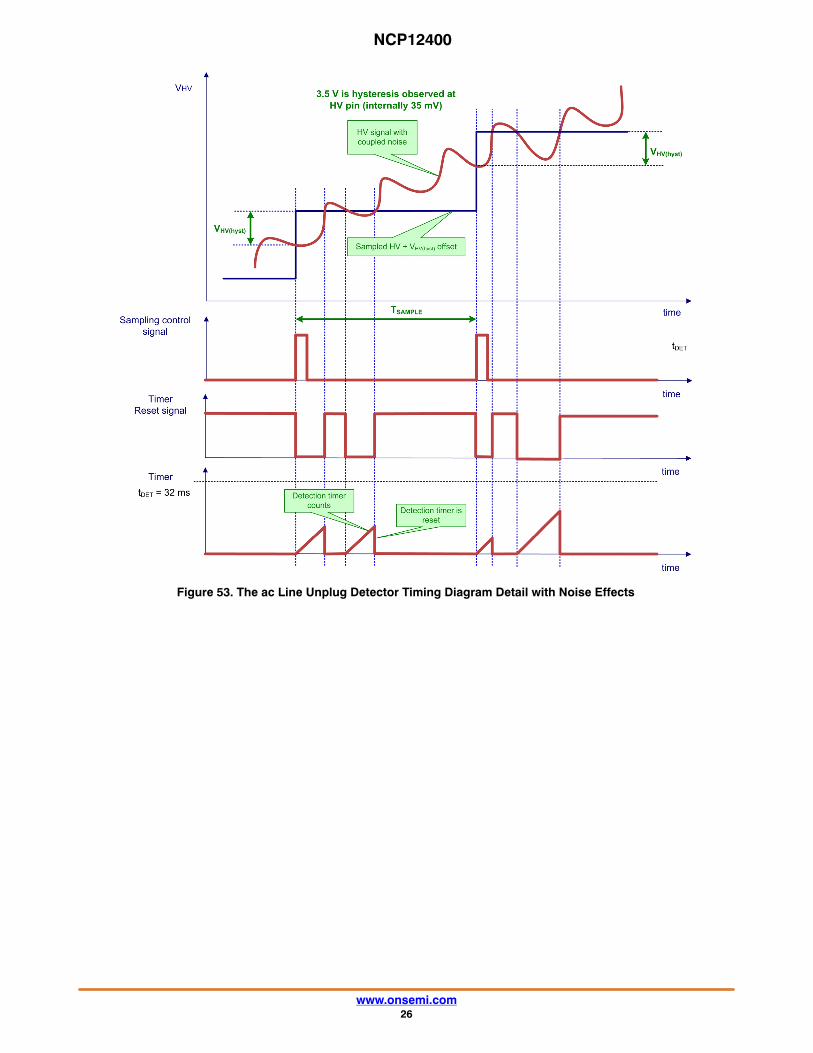
Figure 53. The ac Line Unplug Detector Timing Diagram Detail with Noise Effects

NCP12400
www.onsemi.com27
Figure 54. HV Pin ac Input Timing Diagram with X2 Capacitor Discharge Sequence when the Application isUnplugged Under Extremely Low Line Condition
time
VHV
One Shot
time
DRV
VHV(start)
Startsonly atVCC(on)
VHV(stop)
HVtimerstarts
tDET
Brown−out
HVtimer
restarts
tHV
X2 dischargecurrent
tDIS
X2 discharge
No AC detection
AC line unplug X2 capacitordischarge
AC line Unplugdetector starts
time
VCCVCC(on)
VCC(min)
VCC(dis)
time
time
NCP12400
www.onsemi.com28
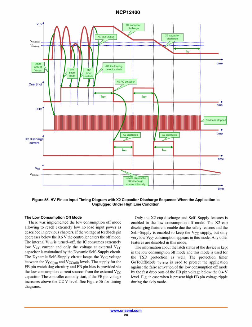
Figure 55. HV Pin ac Input Timing Diagram with X2 Capacitor Discharge Sequence When the Application isUnplugged Under High Line Condition
time
VHV
One Shot
time
DRV
VHV(start)
VHV(stop)
tDET
time
X2 dischargecurrent
t DIS
X2 discharge
AC line unplug
X2 capacitordischarge
AC line Unplugdetector starts
tDET
tDIS
X2 capacitordischarge
Device is stopped
No AC detection
HVtimer
restarts
HVtimerstarts
X2 discharge
Startsonly atVCC(on)
VCC
VCC(dis)
tHV
Device shunts theX2 discharge
current internally
time
time
The Low Consumption Off ModeThere was implemented the low consumption off mode
allowing to reach extremely low no load input power asdescribed in previous chapters. If the voltage at feedback pindecreases below the 0.6 V the controller enters the off mode.The internal VCC is turned−off, the IC consumes extremelylow VCC current and only the voltage at external VCCcapacitor is maintained by the Dynamic Self−Supply circuit.The Dynamic Self−Supply circuit keeps the VCC voltagebetween the VCC(on) and VCC(off) levels. The supply for theFB pin watch dog circuitry and FB pin bias is provided viathe low consumption current sources from the external VCCcapacitor. The controller can only start, if the FB pin voltageincreases above the 2.2 V level. See Figure 56 for timingdiagrams.
Only the X2 cap discharge and Self−Supply features isenabled in the low consumption off mode. The X2 capdischarging feature is enable due the safety reasons and theSelf−Supply is enabled to keep the VCC supply, but onlyvery low VCC consumption appears in this mode. Any otherfeatures are disabled in this mode.
The information about the latch status of the device is keptin the low consumption off mode and this mode is used forthe TSD protection as well. The protection timerGoToOffMode tGTOM is used to protect the applicationagainst the false activation of the low consumption off modeby the fast drop outs of the FB pin voltage below the 0.4 Vlevel. E.g. in case when is present high FB pin voltage rippleduring the skip mode.
NCP12400
www.onsemi.com29
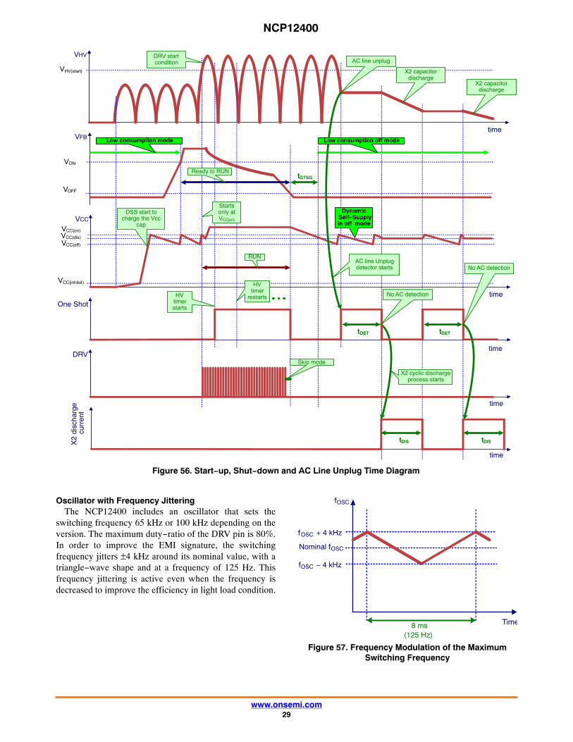
Figure 56. Start−up, Shut−down and AC Line Unplug Time Diagram
time
VHV
time
One Shot
time
DRV
VHV(start)
tDET
X2
disc
harg
ecu
rren
t
time
VCC
VCC(on)
VCC(off)
VCC(inhibit)
VFB
VOFF
VON
Low consumption mode
Ready to RUN
DRV startcondition
DSS start tocharge the Vcc
cap
HVtimerstarts
HVtimer
restarts
AC line Unplugdetector starts
RUN
AC line unplug
X2 capacitordischarge
Startsonly atVCC(on)
VCC(dis)
tDIS
X2 cyclic dischargeprocess starts
tDET
No AC detection
X2 capacitordischarge
tDIS
No AC detection
Low consumption off mode
Skip mode
tGTSG
DynamicSelf−Supplyin off mode
time
Oscillator with Frequency JitteringThe NCP12400 includes an oscillator that sets the
switching frequency 65 kHz or 100 kHz depending on theversion. The maximum duty−ratio of the DRV pin is 80%.In order to improve the EMI signature, the switchingfrequency jitters ±4 kHz around its nominal value, with atriangle−wave shape and at a frequency of 125 Hz. Thisfrequency jittering is active even when the frequency isdecreased to improve the efficiency in light load condition.
Figure 57. Frequency Modulation of the MaximumSwitching Frequency
Time
fOSC
fOSC
8 ms(125 Hz)
Nominal fOSC
fOSC
+ 4 kHz
− 4 kHz
NCP12400
www.onsemi.com30
Low Load Operation Modes: Frequency FoldbackMode (FFM) and Skip Mode
In order to improve the efficiency in light load conditions,the frequency of the internal oscillator is linearly reducedfrom its nominal value down to fOSC(min). This frequencyfoldback starts when the voltage on FB pin goes belowVfb(foldS), and is complete when Vfb reaches Vfb(foldE).The maximum on−time duration control is kept during the
frequency foldback mode to provide the natural transformercore anti−saturation protection. The frequency jittering isstill active while the oscillator frequency decreases as well.The current setpoint is fixed to 300 mV in the frequencyfoldback mode if the feedback voltage decreases below theVfb(freeze) level. This feature increases efficiency underthe light loads conditions as well.
Figure 58. Frequency Foldback Mode Characteristic
FB
Fsw
f OSC
Vskip(in) VFB(foldS)
f OSC(min)
Voffset + K FB X VILIMVFB(foldE)
Vskip(out)
Skip
VFB(freeze)
Fixed I peak
Figure 59. Current Setpoint Dependency on the Feedback Pin Voltage
VFB
Internal current setpoint
VILIMFixed I peak
VI(freeze)
Vskip(in) VFB(foldS)VFB(foldE)
Vskip(out)
VFB(freeze) KFB X VILIM
When the FB voltage reaches Vskip(in) while decreasing,skip mode is activated: the driver stops, and the internalconsumption of the controller is decreased. While VFB isbelow Vskip(out), the controller remains in this state; but assoon as VFB crosses the skip out threshold, the DRV pinstarts to pulse again.
The NCP12400 device includes logic which allows goinginto skip mode after the DRV cycle is finished by reachingof the peak current value. This technique eliminates the lastshort pulses in skip mode, which increases the systemefficiency at light loads and makes easier the application ofactive secondary rectification circuitry.
NCP12400
www.onsemi.com31
Figure 60. Skip Mode Timing Diagram
Figure 61. Technique Preventing Short Pulses in Skip Mode
time
FB
OSC(internal signal)
time
CS
VI(freeze)
Skip signal doesnot immediatelystop the pulse
Vskip(in)
Vskip(out)
Entersskip
time
NCP12400
www.onsemi.com32
Quiet−SkipTo further avoid acoustic noise, the circuit prevents the
burst frequency during skip mode from entering the audiblerange by limiting it to a maximum of 800 Hz. This isachieved via a timer tquiet that is activated duringQuiet−Skip. The start of the next burst cycle is preventeduntil this timer has expired. As the output power decreases,the switching frequency decreases. Once it hits minimumswitching frequency fOSC(min), the skip−in threshold isreached and burst mode is entered − switching stops as soonas the current drive pulses ends – it does not stopimmediately.
Once switching stops, FB will rise. As soon as FB crossesthe skip−exit threshold, drive pulses will resume, but thecontroller remains in burst mode. At this point, a 1250 �s(typ) timer tquiet is started together with a count to nP,skippulses counter. This nP,skip pulses counter ensures theminimum number of DRV signal pulses in burst. The nexttime the FB voltage drops below the skip−in threshold, DRVpulses stop at the end of the current pulse as long as nP,skip
drive pulses have been counted (if not, they do not stop untilthe end of the nP,skip −th pulse). They are not allowed to startagain until the timer expires, even if the skip−exit thresholdis reached first. It is important to note that the timer will notforce the next cycle to begin – i.e. if the natural skipfrequency is such that skip−exit is reached after the timerexpires, the drive pulses will wait for the skip−exitthreshold.
This means that during no−load, there will be a minimumof nP,skip drive pulses, and the burst−cycle period will likelybe much longer than 1250 �s. This operation helps toimprove efficiency at no−load conditions.
In order to exit burst mode, the FB voltage must rise higherthan Vskip(tran) level. If this occurs before tquiet expires, thedrive pulses will resume immediately – i.e. the controllerwon’t wait for the timer to expire. Figure 63 provides anexample of how Quiet−Skip works, while Figure 62 showsthe immediate leaving the quiet skip mode by crossing thetransient enhancement level Vskip(tran).
NCP12400
www.onsemi.com33
Figure 62. Leaving the Quiet−Skip Mode during Load Transient
Figure 63. Quiet−Skip Timing Diagram − option
VFB
Time
DRV
Entersskip
Entersskip
Exits skipafter quiet
timerexpires
Crossing the transientenhancement levelstops the quiet skip
immediatelyVskip(in)
Vskip(out)
Vskip(tran)
tquiet tquiet
Time
DRV
DRV pulses doesnot start because
V FB<V skip (in)
VFB
time
Vskip(out)
Vskip(in)
DRV
VFB
time
Vskip(out)
Vskip(in)
tquiet tquiet
DRVtime
Vskip(out)
Vskip(in)
tquiet tquiet
1
2
3
Sequence of events1 ; 2 ; 3 starts the quiet
skip mode
The DRV pulses does notstart even when VFB >Vskip(out)
in the quiet skip mode
VFB
Vskip(tran)
nP,skip nP,skip
nP,skip
When V FB >Vskip (tran ) the quiet skipmode immediately finishes
Quiet skip modeforces at least n p,skip
pulses in skip modeburst
nP,skipnP,skip
Running just above skipmode with fsw = f osc(min)
time
time
time
NCP12400
www.onsemi.com34
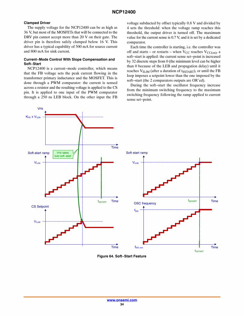
Clamped DriverThe supply voltage for the NCP12400 can be as high as
36 V, but most of the MOSFETs that will be connected to theDRV pin cannot accept more than 20 V on their gate. Thedriver pin is therefore safely clamped below 16 V. Thisdriver has a typical capability of 500 mA for source currentand 800 mA for sink current.
Current−Mode Control With Slope Compensation andSoft−Start
NCP12400 is a current−mode controller, which meansthat the FB voltage sets the peak current flowing in thetransformer primary inductance and the MOSFET. This isdone through a PWM comparator: the current is sensedacross a resistor and the resulting voltage is applied to the CSpin. It is applied to one input of the PWM comparatorthrough a 250 ns LEB block. On the other input the FB
voltage subducted by offset typically 0.8 V and divided by4 sets the threshold: when the voltage ramp reaches thisthreshold, the output driver is turned off. The maximumvalue for the current sense is 0.7 V, and it is set by a dedicatedcomparator.
Each time the controller is starting, i.e. the controller wasoff and starts – or restarts – when VCC reaches VCC(on), asoft−start is applied: the current sense set−point is increasedby 32 discrete steps from 0 (the minimum level can be higherthan 0 because of the LEB and propagation delay) until itreaches VILIM (after a duration of tSSTART), or until the FBloop imposes a setpoint lower than the one imposed by thesoft−start (the 2 comparators outputs are OR’ed).
During the soft−start the oscillator frequency increasefrom the minimum switching frequency to the maximumswitching frequency following the ramp applied to currentsense set−point.
Figure 64. Soft−Start Feature
Time
CS Setpoint
Soft−start ramp VFB takesover soft −start
tSSTART
Time
VFB
VILIM
VILIM
KFB x VILIM
Time
OSC frequency
Soft−start ramp
tSSTART
VILIM
fSW
tSSTART
fSW ,min
TimeTime
NCP12400
www.onsemi.com35
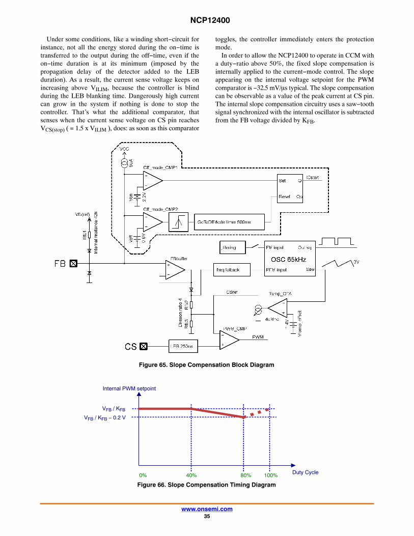
Under some conditions, like a winding short−circuit forinstance, not all the energy stored during the on−time istransferred to the output during the off−time, even if theon−time duration is at its minimum (imposed by thepropagation delay of the detector added to the LEBduration). As a result, the current sense voltage keeps onincreasing above VILIM, because the controller is blindduring the LEB blanking time. Dangerously high currentcan grow in the system if nothing is done to stop thecontroller. That’s what the additional comparator, thatsenses when the current sense voltage on CS pin reachesVCS(stop) ( = 1.5 x VILIM ), does: as soon as this comparator
toggles, the controller immediately enters the protectionmode.
In order to allow the NCP12400 to operate in CCM witha duty−ratio above 50%, the fixed slope compensation isinternally applied to the current−mode control. The slopeappearing on the internal voltage setpoint for the PWMcomparator is −32.5 mV/�s typical. The slope compensationcan be observable as a value of the peak current at CS pin.The internal slope compensation circuitry uses a saw−toothsignal synchronized with the internal oscillator is subtractedfrom the FB voltage divided by KFB.
Figure 65. Slope Compensation Block Diagram
Figure 66. Slope Compensation Timing Diagram
Duty Cycle
Internal PWM setpoint
40% 100%80%0%
VFB / KFB − 0.2 V
VFB / KFB
NCP12400
www.onsemi.com36
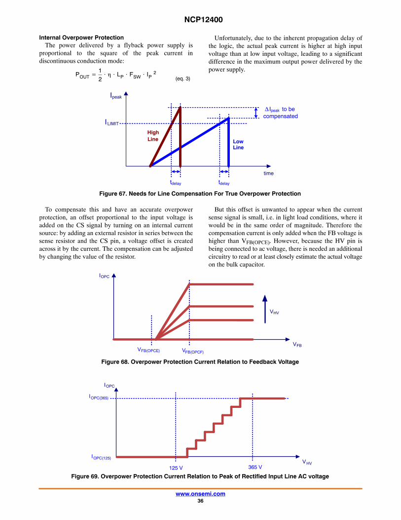
Internal Overpower ProtectionThe power delivered by a flyback power supply is
proportional to the square of the peak current indiscontinuous conduction mode:
POUT �
1
2� � � LP � FSW � IP
2(eq. 3)
Unfortunately, due to the inherent propagation delay ofthe logic, the actual peak current is higher at high inputvoltage than at low input voltage, leading to a significantdifference in the maximum output power delivered by thepower supply.
Figure 67. Needs for Line Compensation For True Overpower Protection
time
Ipeak
HighLine Low
Line
ILIMIT
tdelay tdelay
� Ipeak to becompensated
To compensate this and have an accurate overpowerprotection, an offset proportional to the input voltage isadded on the CS signal by turning on an internal currentsource: by adding an external resistor in series between thesense resistor and the CS pin, a voltage offset is createdacross it by the current. The compensation can be adjustedby changing the value of the resistor.
But this offset is unwanted to appear when the currentsense signal is small, i.e. in light load conditions, where itwould be in the same order of magnitude. Therefore thecompensation current is only added when the FB voltage ishigher than VFB(OPCE). However, because the HV pin isbeing connected to ac voltage, there is needed an additionalcircuitry to read or at least closely estimate the actual voltageon the bulk capacitor.
Figure 68. Overpower Protection Current Relation to Feedback Voltage
VFB
IOPC
VFB(OPCE) VFB(OPCF)
VHV
Figure 69. Overpower Protection Current Relation to Peak of Rectified Input Line AC voltage
VHV
IOPC
365 V125 V
IOPC(125)
IOPC(365)
NCP12400
www.onsemi.com37
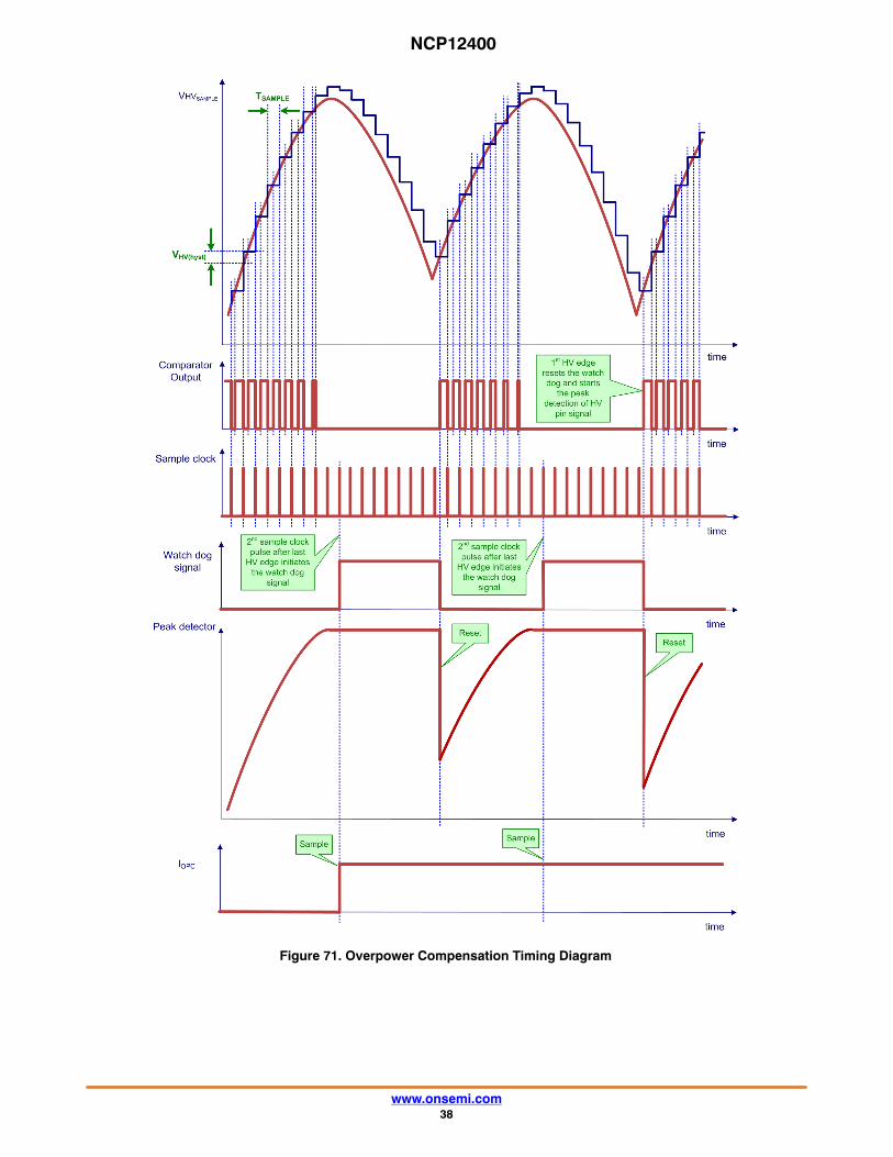
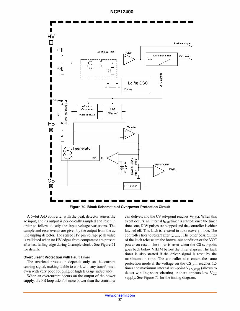
Figure 70. Block Schematic of Overpower Protection Circuit
A 5−bit A/D converter with the peak detector senses theac input, and its output is periodically sampled and reset, inorder to follow closely the input voltage variations. Thesample and reset events are given by the output from the acline unplug detector. The sensed HV pin voltage peak valueis validated when no HV edges from comparator are presentafter last falling edge during 2 sample clocks. See Figure 71for details.
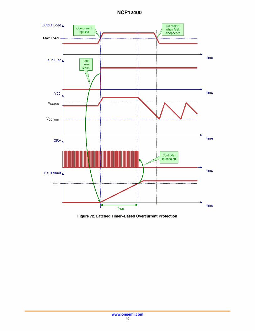
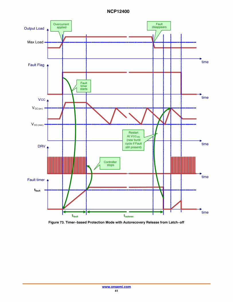
Overcurrent Protection with Fault TimerThe overload protection depends only on the current
sensing signal, making it able to work with any transformer,even with very poor coupling or high leakage inductance.
When an overcurrent occurs on the output of the powersupply, the FB loop asks for more power than the controller
can deliver, and the CS set−point reaches VILIM. When thisevent occurs, an internal tfault timer is started: once the timertimes out, DRV pulses are stopped and the controller is eitherlatched off. This latch is released in autorecovery mode. Thecontroller tries to restart after tautorec. The other possibilitiesof the latch release are the brown−out condition or the VCCpower on reset. The timer is reset when the CS set−pointgoes back below VILIM before the timer elapses. The faulttimer is also started if the driver signal is reset by themaximum on time. The controller also enters the sameprotection mode if the voltage on the CS pin reaches 1.5times the maximum internal set−point VCS(stop) (allows todetect winding short−circuits) or there appears low VCCsupply. See Figure 71 for the timing diagram.
NCP12400
www.onsemi.com39
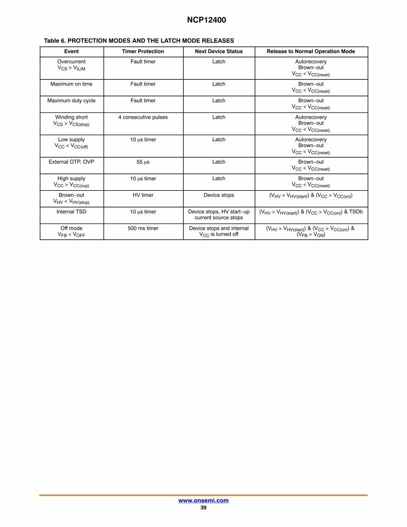
Table 6. PROTECTION MODES AND THE LATCH MODE RELEASES
Event Timer Protection Next Device Status Release to Normal Operation Mode
OvercurrentVCS > VILIM
Fault timer Latch AutorecoveryBrown−out
VCC < VCC(reset)
Maximum on time Fault timer Latch Brown−outVCC < VCC(reset)
Maximum duty cycle Fault timer Latch Brown−outVCC < VCC(reset)
Winding shortVCS > VCS(stop)
4 consecutive pulses Latch AutorecoveryBrown−out
VCC < VCC(reset)
Low supplyVCC < VCC(off)
10 �s timer Latch AutorecoveryBrown−out
VCC < VCC(reset)
External OTP, OVP 55 �s Latch Brown−outVCC < VCC(reset)
High supplyVCC > VCC(ovp)
10 �s timer Latch Brown−outVCC < VCC(reset)
Brown−outVHV < VHV(stop)
HV timer Device stops (VHV > VHV(start)) & (VCC > VCC(on))
Internal TSD 10 �s timer Device stops, HV start−upcurrent source stops
(VHV > VHV(start)) & (VCC > VCC(on)) & TSDb
Off modeVFB < VOFF
500 ms timer Device stops and internalVCC is turned off
(VHV > VHV(start)) & (VCC > VCC(on)) & (VFB > VON)
NCP12400
www.onsemi.com40
VCC(on)
VCC(min)
Figure 72. Latched Timer−Based Overcurrent Protection
NCP12400
www.onsemi.com41
Figure 73. Timer−based Protection Mode with Autorecovery Release from Latch−off
time
Fault Flag
time
VCC
time
DRV
VCC (on )
VCC (min)
Overcurrentapplied
time
Output Load
Max Load
time
Fault timer
Faulttimerstarts
Controllerstops
Faultdisappears
tfault tautorec
RestartAt VCC ON
(new burstcycle if Faultstill present)
tfault
NCP12400
www.onsemi.com42
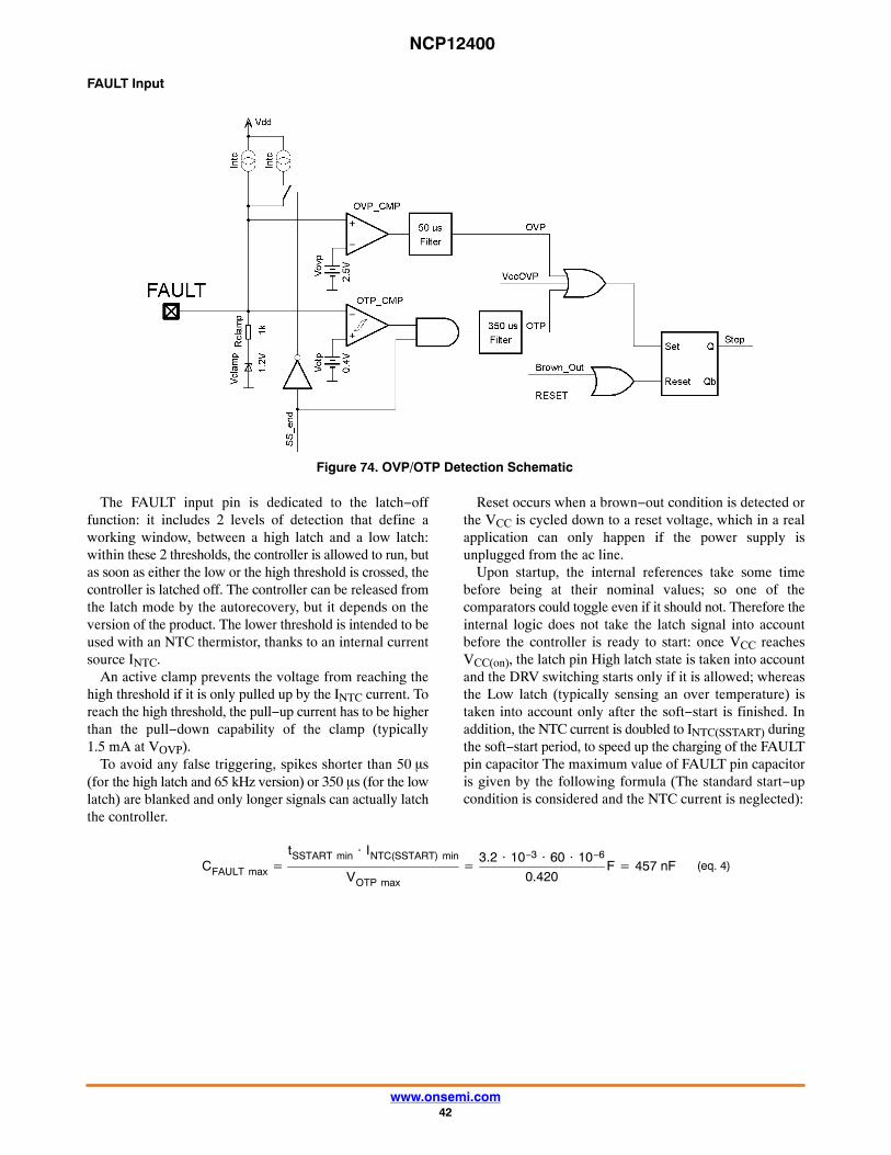
FAULT Input
Figure 74. OVP/OTP Detection Schematic
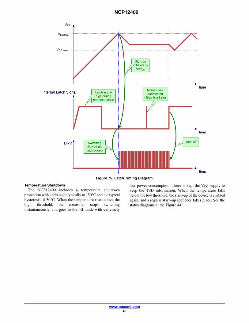
The FAULT input pin is dedicated to the latch−offfunction: it includes 2 levels of detection that define aworking window, between a high latch and a low latch:within these 2 thresholds, the controller is allowed to run, butas soon as either the low or the high threshold is crossed, thecontroller is latched off. The controller can be released fromthe latch mode by the autorecovery, but it depends on theversion of the product. The lower threshold is intended to beused with an NTC thermistor, thanks to an internal currentsource INTC.
An active clamp prevents the voltage from reaching thehigh threshold if it is only pulled up by the INTC current. Toreach the high threshold, the pull−up current has to be higherthan the pull−down capability of the clamp (typically1.5 mA at VOVP).
To avoid any false triggering, spikes shorter than 50 �s(for the high latch and 65 kHz version) or 350 �s (for the lowlatch) are blanked and only longer signals can actually latchthe controller.
Reset occurs when a brown−out condition is detected orthe VCC is cycled down to a reset voltage, which in a realapplication can only happen if the power supply isunplugged from the ac line.
Upon startup, the internal references take some timebefore being at their nominal values; so one of thecomparators could toggle even if it should not. Therefore theinternal logic does not take the latch signal into accountbefore the controller is ready to start: once VCC reachesVCC(on), the latch pin High latch state is taken into accountand the DRV switching starts only if it is allowed; whereasthe Low latch (typically sensing an over temperature) istaken into account only after the soft−start is finished. Inaddition, the NTC current is doubled to INTC(SSTART) duringthe soft−start period, to speed up the charging of the FAULTpin capacitor The maximum value of FAULT pin capacitoris given by the following formula (The standard start−upcondition is considered and the NTC current is neglected):
CFAULT max �
tSSTART min � INTC(SSTART) min
VOTP max
�
3.2 � 10−3� 60 � 10−6
0.420F � 457 nF (eq. 4)
NCP12400
www.onsemi.com43
Figure 75. Latch Timing Diagram
VCC(on)
VCC(min)
Temperature ShutdownThe NCP12400 includes a temperature shutdown
protection with a trip point typically at 150°C and the typicalhysteresis of 30°C. When the temperature rises above thehigh threshold, the controller stops switchinginstantaneously, and goes to the off mode with extremely
low power consumption. There is kept the VCC supply tokeep the TSD information. When the temperature fallsbelow the low threshold, the start−up of the device is enabledagain, and a regular start−up sequence takes place. See thestatus diagrams at the Figure 44.
NCP12400
www.onsemi.com44
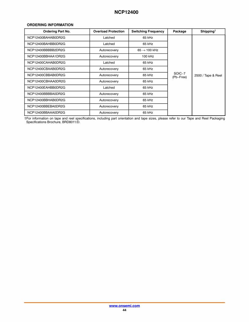
ORDERING INFORMATION
Ordering Part No. Overload Protection Switching Frequency Package Shipping†
NCP12400BAHAB0DR2G Latched 65 kHz
SOIC−7(Pb−Free) 2500 / Tape & Reel
NCP12400BAHBB0DR2G Latched 65 kHz
NCP12400BBBBB2DR2G Autorecovery 65 → 100 kHz
NCP12400BBHAA1DR2G Autorecovery 100 kHz
NCP12400CAHAB0DR2G Latched 65 kHz
NCP12400CBAAB0DR2G Autorecovery 65 kHz
NCP12400CBBAB0DR2G Autorecovery 65 kHz
NCP12400CBHAA0DR2G Autorecovery 65 kHz
NCP12400EAHBB0DR2G Latched 65 kHz
NCP12400BBBBA0DR2G Autorecovery 65 kHz
NCP12400BBHAB0DR2G Autorecovery 65 kHz
NCP12400BBEBA0DR2G Autorecovery 65 kHz
NCP12400BBAAA0DR2G Autorecovery 65 kHz
†For information on tape and reel specifications, including part orientation and tape sizes, please refer to our Tape and Reel PackagingSpecifications Brochure, BRD8011/D.
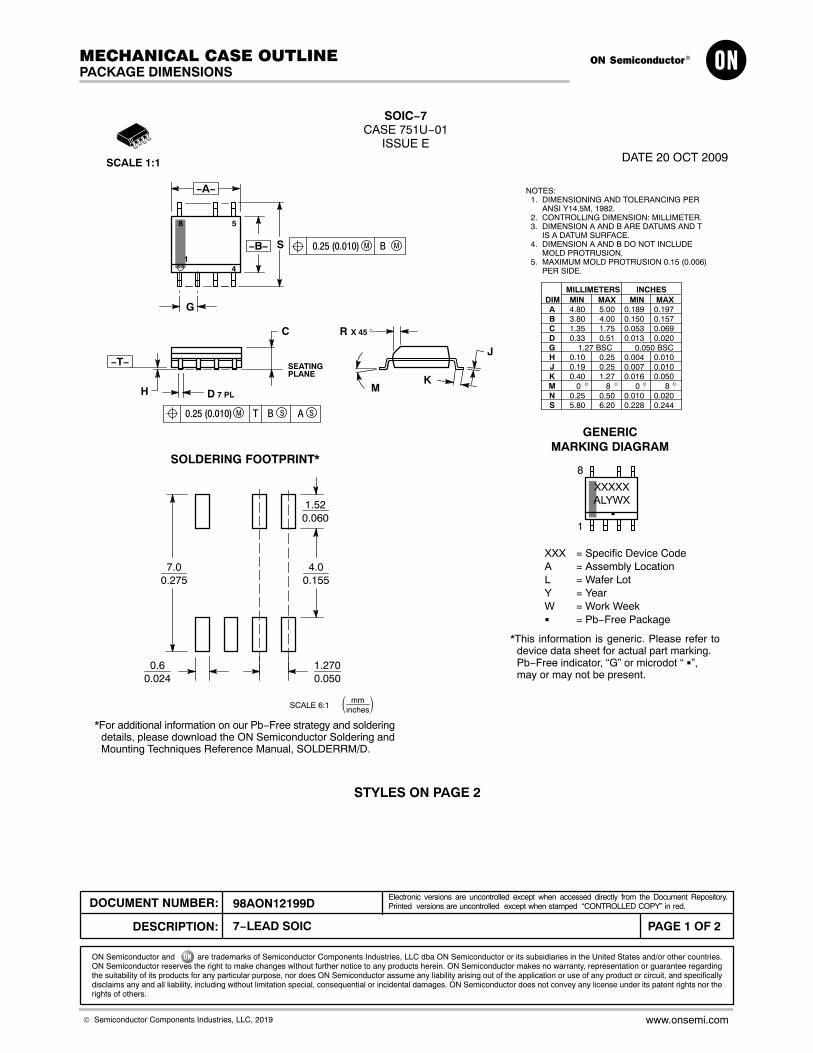
SOIC−7CASE 751U−01
ISSUE EDATE 20 OCT 2009
SEATINGPLANE
14
58
R
J
X 45�
K
NOTES:1. DIMENSIONING AND TOLERANCING PER
ANSI Y14.5M, 1982.2. CONTROLLING DIMENSION: MILLIMETER.3. DIMENSION A AND B ARE DATUMS AND T
IS A DATUM SURFACE.4. DIMENSION A AND B DO NOT INCLUDE
MOLD PROTRUSION.5. MAXIMUM MOLD PROTRUSION 0.15 (0.006)
PER SIDE.
S
DH
C
SCALE 1:1
DIMA
MIN MAX MIN MAXINCHES
4.80 5.00 0.189 0.197
MILLIMETERS
B 3.80 4.00 0.150 0.157C 1.35 1.75 0.053 0.069D 0.33 0.51 0.013 0.020G 1.27 BSC 0.050 BSCH 0.10 0.25 0.004 0.010J 0.19 0.25 0.007 0.010K 0.40 1.27 0.016 0.050M 0 8 0 8 N 0.25 0.50 0.010 0.020S 5.80 6.20 0.228 0.244
−A−
−B−
G
MBM0.25 (0.010)
−T−
BM0.25 (0.010) T S A S
M
XXX = Specific Device CodeA = Assembly LocationL = Wafer LotY = YearW = Work Week� = Pb−Free Package
GENERICMARKING DIAGRAM
7 PL� � � �
*This information is generic. Please refer todevice data sheet for actual part marking.Pb−Free indicator, “G” or microdot “ �”,may or may not be present.
XXXXXALYWX
�1
8
STYLES ON PAGE 2
1.520.060
7.00.275
0.60.024
1.2700.050
4.00.155
� mminches
�SCALE 6:1
*For additional information on our Pb−Free strategy and solderingdetails, please download the ON Semiconductor Soldering andMounting Techniques Reference Manual, SOLDERRM/D.
SOLDERING FOOTPRINT*
MECHANICAL CASE OUTLINE
PACKAGE DIMENSIONS
ON Semiconductor and are trademarks of Semiconductor Components Industries, LLC dba ON Semiconductor or its subsidiaries in the United States and/or other countries.ON Semiconductor reserves the right to make changes without further notice to any products herein. ON Semiconductor makes no warranty, representation or guarantee regardingthe suitability of its products for any particular purpose, nor does ON Semiconductor assume any liability arising out of the application or use of any product or circuit, and specificallydisclaims any and all liability, including without limitation special, consequential or incidental damages. ON Semiconductor does not convey any license under its patent rights nor therights of others.
98AON12199DDOCUMENT NUMBER:
DESCRIPTION:
Electronic versions are uncontrolled except when accessed directly from the Document Repository.Printed versions are uncontrolled except when stamped “CONTROLLED COPY” in red.
PAGE 1 OF 27−LEAD SOIC
© Semiconductor Components Industries, LLC, 2019 www.onsemi.com
SOIC−7CASE 751U−01
ISSUE EDATE 20 OCT 2009
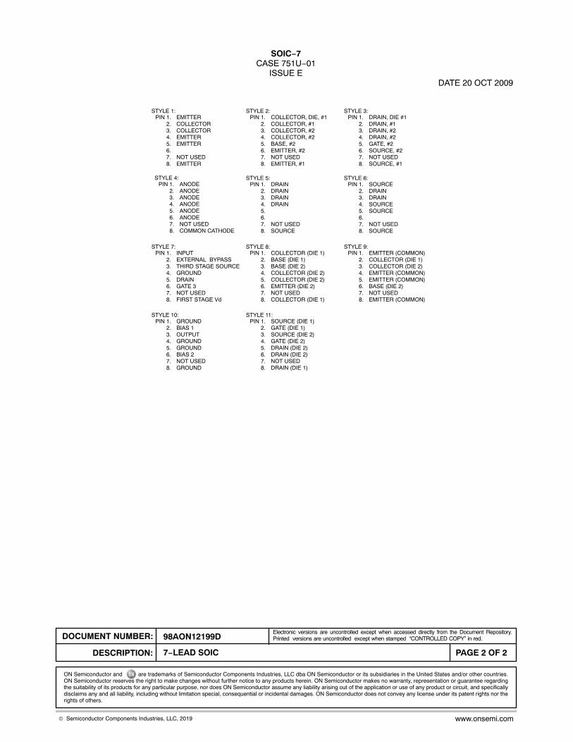
STYLE 4:PIN 1. ANODE
2. ANODE3. ANODE4. ANODE5. ANODE6. ANODE7. NOT USED8. COMMON CATHODE
STYLE 1:PIN 1. EMITTER
2. COLLECTOR3. COLLECTOR4. EMITTER5. EMITTER6.7. NOT USED8. EMITTER
STYLE 2:PIN 1. COLLECTOR, DIE, #1
2. COLLECTOR, #13. COLLECTOR, #24. COLLECTOR, #25. BASE, #26. EMITTER, #27. NOT USED8. EMITTER, #1
STYLE 3:PIN 1. DRAIN, DIE #1
2. DRAIN, #13. DRAIN, #24. DRAIN, #25. GATE, #26. SOURCE, #27. NOT USED8. SOURCE, #1
STYLE 6:PIN 1. SOURCE
2. DRAIN3. DRAIN4. SOURCE5. SOURCE6.7. NOT USED8. SOURCE
STYLE 5:PIN 1. DRAIN
2. DRAIN3. DRAIN4. DRAIN5.6.7. NOT USED8. SOURCE
STYLE 7:PIN 1. INPUT
2. EXTERNAL BYPASS3. THIRD STAGE SOURCE4. GROUND5. DRAIN6. GATE 37. NOT USED8. FIRST STAGE Vd
STYLE 8:PIN 1. COLLECTOR (DIE 1)
2. BASE (DIE 1)3. BASE (DIE 2)4. COLLECTOR (DIE 2)5. COLLECTOR (DIE 2)6. EMITTER (DIE 2)7. NOT USED8. COLLECTOR (DIE 1)
STYLE 9:PIN 1. EMITTER (COMMON)
2. COLLECTOR (DIE 1)3. COLLECTOR (DIE 2)4. EMITTER (COMMON)5. EMITTER (COMMON)6. BASE (DIE 2)7. NOT USED8. EMITTER (COMMON)
STYLE 10:PIN 1. GROUND
2. BIAS 13. OUTPUT4. GROUND5. GROUND6. BIAS 27. NOT USED8. GROUND
STYLE 11:PIN 1. SOURCE (DIE 1)
2. GATE (DIE 1)3. SOURCE (DIE 2)4. GATE (DIE 2)5. DRAIN (DIE 2)6. DRAIN (DIE 2)7. NOT USED8. DRAIN (DIE 1)
ON Semiconductor and are trademarks of Semiconductor Components Industries, LLC dba ON Semiconductor or its subsidiaries in the United States and/or other countries.ON Semiconductor reserves the right to make changes without further notice to any products herein. ON Semiconductor makes no warranty, representation or guarantee regardingthe suitability of its products for any particular purpose, nor does ON Semiconductor assume any liability arising out of the application or use of any product or circuit, and specificallydisclaims any and all liability, including without limitation special, consequential or incidental damages. ON Semiconductor does not convey any license under its patent rights nor therights of others.
98AON12199DDOCUMENT NUMBER:
DESCRIPTION:
Electronic versions are uncontrolled except when accessed directly from the Document Repository.Printed versions are uncontrolled except when stamped “CONTROLLED COPY” in red.
PAGE 2 OF 27−LEAD SOIC
© Semiconductor Components Industries, LLC, 2019 www.onsemi.com
onsemi, , and other names, marks, and brands are registered and/or common law trademarks of Semiconductor Components Industries, LLC dba “onsemi” or its affiliatesand/or subsidiaries in the United States and/or other countries. onsemi owns the rights to a number of patents, trademarks, copyrights, trade secrets, and other intellectual property.A listing of onsemi’s product/patent coverage may be accessed at www.onsemi.com/site/pdf/Patent−Marking.pdf. onsemi reserves the right to make changes at any time to anyproducts or information herein, without notice. The information herein is provided “as−is” and onsemi makes no warranty, representation or guarantee regarding the accuracy of theinformation, product features, availability, functionality, or suitability of its products for any particular purpose, nor does onsemi assume any liability arising out of the application or useof any product or circuit, and specifically disclaims any and all liability, including without limitation special, consequential or incidental damages. Buyer is responsible for its productsand applications using onsemi products, including compliance with all laws, regulations and safety requirements or standards, regardless of any support or applications informationprovided by onsemi. “Typical” parameters which may be provided in onsemi data sheets and/or specifications can and do vary in different applications and actual performance mayvary over time. All operating parameters, including “Typicals” must be validated for each customer application by customer’s technical experts. onsemi does not convey any licenseunder any of its intellectual property rights nor the rights of others. onsemi products are not designed, intended, or authorized for use as a critical component in life support systemsor any FDA Class 3 medical devices or medical devices with a same or similar classification in a foreign jurisdiction or any devices intended for implantation in the human body. ShouldBuyer purchase or use onsemi products for any such unintended or unauthorized application, Buyer shall indemnify and hold onsemi and its officers, employees, subsidiaries, affiliates,and distributors harmless against all claims, costs, damages, and expenses, and reasonable attorney fees arising out of, directly or indirectly, any claim of personal injury or deathassociated with such unintended or unauthorized use, even if such claim alleges that onsemi was negligent regarding the design or manufacture of the part. onsemi is an EqualOpportunity/Affirmative Action Employer. This literature is subject to all applicable copyright laws and is not for resale in any manner.
PUBLICATION ORDERING INFORMATIONTECHNICAL SUPPORTNorth American Technical Support:Voice Mail: 1 800−282−9855 Toll Free USA/CanadaPhone: 011 421 33 790 2910
LITERATURE FULFILLMENT:Email Requests to: [email protected]
onsemi Website: www.onsemi.com
Europe, Middle East and Africa Technical Support:Phone: 00421 33 790 2910For additional information, please contact your local Sales Representative
◊