Embed Size (px)
Citation preview

NOTE TO USERS
This reproduction is the best copy available.
muD

An Assessrnent of VLSI and Embedded Software Implementations
for Reed-Solomon Decoders
Ted S. Fill
A Thesis submitted in conformity with the requirements for the degree of Master of Applied Scienpe,
Edward S. Rogers Sr. Department of Electrical and Cornputer Engineering, University of Toronto
O Copyright by Ted S. Fill2001
National Library 1+1 ,,da Bibliothèque nationale du Canada
Acquisitions and Acquisitions et Bibliographie Services services bibliographiques 385 WeYingîcm Street 395, rue Wellington OfrawaON KlAON4 OîtawaûN K 1 A W Canada canada
The author has granted a non- exclusive licence dowing the National Library of Canada to reproduce, Ioan, distribute or seii copies of this thesis in microfom, paper or electronic formats.
The author retains ownership of the copyright in this thesis. Neither the îhesis nor substantial extracts fiorn it may be printed or otherwise reproduced without the author's permission.
L'auteur a accordé me licence non exclusive permettant à la Bibliothèque nationale du Canada de reproduire, prêter, distribuer ou vendre des copies de cette thèse sous la forme de microfiche/film, de reproduction sur papier ou sur format électronique.
L'auteur conserve la propriété du droit d'auteur qui protège cette thèse. Ni la thèse ni des extraits substantiels de celle-ci ne doivent être imprimés ou autrement reproduits sans son autorisation.
An Assessrnent of
VLSI and Embedded Software Implementations
for
Red-Solomon Decoders
Ted Stanley Fil1
Master of Applied Science, 200 1
Edward S. Rogers Sr. Department of Electrical and Cornputer Engineering
University of Toronto
Abstract
Reed-Solomon decoders are used extensively in numerous applications ranging from cellular
telephones to deep-space communications. This thesis examined Reed-Solomon time-domain
and frequency-domain decoder implementations in both software and hardware. Thus far,
there have been no clear, definitive statements in the published literature about the relative
merits and limitations of each type of decoder implementation. In response, a detailed
cornparison is presented through tangible results from dedicated hardware and software
implementations. The focus was on designing area-efficient, low-power and iow-complexity
decoders suitable for today's moderate rate applications. Two decoder chips were designed in
a 0.18pm CMOS process and they targeted a decoding rate of 160 Mbps. The time-domain
decoder was fabricated and had a core area of 1.50 mm2 and an overall silicon die area of
3.54 mm2.

iii

Acknowledgments
At times it seemed unreachable and unending, but this thesis is b d y complete. It would
not have been possible without the help and generosity of many people.
Sincere thanks to rny advisor Professor Glenn Gulak for his ideas, support and
encouragement throughout this thesis. Th&-you Glenn for your guidance and advice.
Financial assistance from NSERC as well as fabrication support f?om CMC were greatly
appreciated.
Special mention goes out to Kostas Pagiamtzis for all his help with the memory cores and
suggestions for the design flow. Thanks Kos. 1 would also like to thank Vincent Gaudet for
his much appreciated help and with the chip testing . May the West be strong.
Thanks to al1 my fkiends in PT392 and EECG induding: Ahmad, Ajay, Amy, Andy, Dave,
Derek, Elias, Guy, Leslie, Mark, Marcus, Nirmal, Paul, Peter, Roman, Shahriar, Sirish, Tor,
Tooraj, Warren, William, and Yadi.
Peace to the Westside UofX boyz fkom Edmonton: Brad, Dan, Erik, Jax, Kelly, Matt, Michael,
Rob, and Vinesh. City of Champions forever.
Most of d, 1 am extremely grateful to my family for their love, understanding and support.
It's finally done! Thanks Gerty for all your help and dl tha t you have done for me in Toronto.
To my sisters Carolin and Teresa: thanks so much for your continued support which helped
me get through this. I would especially like to express my utmost sincere appreciation,
thanks and love to my Mom and Dad for their never-ending encouragement. Dreams are
possible with loving parents like you.

Contents C-R 1 Introduction 1
1.1 Motivation ............................................................................................................. 1
............................................................................................................. 1.2 Objectives 2
................................................................................................... 1.3 Thesis O v e ~ e w -3
CHAPTER 2 Reed-Solomon Decoding 5 ............................................................................................................ 2.1 Block Codes 5
........................................................................... 2.1.1 Forward Error Correction 7 ................................................................................... 2.1.2 Reed-Solomon Codes 8
.................................................................................................. 2.1.3 Applications 11 .................................................................... 2.2 Reed-Solomon Decoding Algorithms 13 .................................................................... 2.2.1 Berlekamp-Massey Algorithm 15 .................................................................... 2.2.2 Modified Euclidean Algorithm 16
......................................................................... 2.2.3 Other Decoding Algorithms 17 ............................................ 2.3 Previous Reed-Solomon Decoder Implementations 19
.............................................................................................................. 2.4 Summary 2 9
CHAPTER 3 Reed-Solomon Decoder Design 31 ................................................................................... 3.1 Implementation Overview 3 1
......................................................................................... 3.2 Syndrome Calculation 3 4 ................................................................................................. 3.3 Erasure Handling 35
......................................................................................... 3.4 Polynomial Generation 36 ........................................................................ 3.4.1 Erasure Locator Polynomial 36
..................................................................... 3.4.2 Forney Syndrome Polynomial 37 ............................................................................ 3.5 Modified Euclidean Algorithm 3 8 ............................................................................. 3.6 Time-Domain Decoder Output 39
.................................................................... 3.7 Frequency-Domain Decoder Output 42 ...................................................................... 3.7.1 Remaining Error Transform 4 2
............................................................................ 3.7.2 Inverse Error Transform 4 3 ............................................................................................................... 3.8 Summary 44
CHAPTER 4 Reed-Solomon Hardware Implementation 47 ................................................................ 4.1 Reed-Solomon Time-Domain Decoder 4 7
....................................................................................... 4.1.1 VLSI Architecture 4 8 .............................................................................. 4.1.2 Implementation Results 56 ........................................................................... 4.1.3 ASIC Fabrication Testing 5 9
........................................................ 4.2 ReedSolomon Frequency-Domain Decoder 59
....................................................................................... 4.2.1 VLSI Architecture 6 0 ............................................................................. 4.2.2 Implementation Results 6 2
.......................................................................................................... 4.2.3 Testing 64
4.3 Comparative Analysis of Time and Frequency Domain Irnplementations ....... 64
............................................................................................................... 4.4 Summary 70
CHAPTER 5 Reed-Solomon Software Implementation 73
........................................................................................... 5.1 System Specifications 73
........................................................................... 5.2 Tirne-Domain Decoding Results 74
.................................................................. 5.3 Frequency-Domain Decoding Results 77
................................................................. 5.4 Comparative Analysis and Summary 79
CBAPTER 6 Conclusions 83
............................................................................................................... 6.1 Summary 83
........................................................................................................... 6.2 Conclusions 84
6.3 Contributions of this Thesis ................................................................................. 85
6.4 Future Research ................................................................................................... 85 ........................................................... 6.4.1 Reed-Solomon Decoding Algorithms 85 ......................................................... 6.4.2 ASIC Design Methodology and Flow 8 6
..................................................... 6.4.3 Galois Field Architecture Cornparisons 8 6
References 87
APPENDIX A Galois Field Primer 93
APPENDIX B Reed-Solomon MATLAB Code 97
APPENDIX C Software Profiling Results 117
v i i
List of Tables 2-1 RS Code Modifiers ............................................................................................................ 9
2-2 Applications and their Corresponding RS Code Specifications ..................................... 13
2-3 RS Decoder Implementation Literature Summary ........................................................ 27
3-1 Decoder Elements as a Function of Code Parameters .................................................. 44
4-1 Non-Optimized Hardware Requirements for (255, 239) RS Decoders ........................... 48
4-2 RS Decoder y0 Pin Description ..................................................................................... 57
4-3 Reed-Solomon TDD VLSI Results ................................................................................... 58
4-4 Reed-Solomon FDD VLSI Results ................................................................................... 63
........................................................................... 4-5 Reed-Solomon Decoder Cornparison 6 5
4-6 RS Decoder Thesis Summary for Table 2-3 .................................................................... 69
5-1 TDD Software Implementation Results ......................................................................... 74
5-2 Compiler Optimization Methods ..................................................................................... 75
5-3 TDD Software Static Memory Usage Results ................................................................ 77
5-4 FDD Software Implementation Results .......................................................................... 78
................................................................. 5-5 FDD Software Static Memory Usage Results 79
................................................ 5-6 Summary of Software Implementation of RS Decoders 8 1
4 3 A-1 G F ( ~ ~ ) Based on the Primitive Polynomial x + x + 1 ................................................. 95
............................................................................ C-1 Profiler Process Name Explanations 117
........................................................................... C-2 Sample TDD gprof Profiling Session 118
C m 3 Sample FDD gprof Profiling Session ......................................................................... 120
viii

List of Figures 1-1 Comparing the Performance of Two Platforms and Two Domains ............................... 3
2-1 Mode1 for an additive noisy communication chanael Wick19951 ................................. 6
................................................................ 2-2 Reed-Solomon Decoder Outline and Timeline 29
3-1 Structural O v e ~ e w of the Time Domain Decoder ................................................... 32
3-2 Structural Overview of the Frequency Domain Decoder .......................................... 33
.............................................................................. 3-3 Generic Syndrome Calculation Unit 3 5
k ............................................................................................. 3-4 Generic a Generation Unit 36
............................................ 3-5 Erasure Locator Polynomial Generation Unit [HsTr1988] 36
......................................... 3-6 Forney Syndrome Polynomial Generation Unit msTr19881 37
.............................................................................. 3-7 One Recursive MEA Ce11 [Shao1988] 40
.......................................................... 3-8 Polynomial Evaluation Circuit for o ( x ) and o B ( x ) 41
................................................................................. 3-9 Remaining Error Transform Block 42
..................................................................................... 3-10 Inverse Error Transform Block 43
................................................................................................... 4-1 Memory Block Partition 50
................................................................................................ 4-2 Memory Interface Circuit 51
............................................................................................. 4-3 Syndrome Calculation Unit 51
k ......................................................................................................... 4-4 cc Generation Block 52
.............................................. 4-5 Modified Erasure Locator Polynomial Generation Block 53
........................................... 4-6 Modified Forney Syndrome Polynomial Generation Block 5 3
4-7 Modified Chien Search Block .......................................................................................... 54
................................................................................................................. 4-8 TDD Die Photo 59
4-9 Error Transform Block ..................................................................................................... 60
.............................................................................................. 4-10 Inverse Transform Block 6 1
........................................................................................ 4-1 1 FDD Pre-Fabrication Layout 6 4

List of Symbols Reed-Solomon Codeword.
Minimum distance of an error correction code.
ith coefficient of the inverse transform of the error pattern (for the FDD).
ith errata pattern magnitude (for the TDD).
Number of information symbols in a Reed-Solomon Code.
Size in bits of the Galois Field.
Codeword length, in symbols, of a Reed-Solomon Code.
Received Reed-Solomon input codeword.
ith received input symbol.
Error correcting capability of an Reed-Solomon code.
Number of erasures.
ith output codeword symbol.
ith e m transfo- coefficient.
Syndrome polynomial.
kth coefficient of the syndrome polynomial.
Forney syndrome polynomial
kth coefficient of the Forney syndrome polynomial.
Primitive element in a Galois Field.
Errata locator polynomial.
Errata magnitude polynomial.
Erasure locator polynomial.
xii

List of Acronyms ADSL
ARQ
ASIC
BER
BM
CCSDS
CD
CDMA
CLB
CMOS
DFT
DG
DOCSIS
DVB
DVD
DSM
FD
FDD
FEC
FPGA
GCD
Asymmetrical Digital Subscriber Line
Automatic Repeat Request
Application Specific Integrated Circuit
Bit Error Rate
Berlekamp-Massey
Consultative Committee for Space Data Systems
Compact Disc
Code Division Multiple Access
Configurable Logic Block
Complement ary Metal Oxide Semiconductor
Discrete Fourier Trausform
Dependence Graph
Data-Over-Cable Service Interface Specification
Digital Video Broadcasting
Digital Versatile Disc
Deep Submicron
Frequency-Domain
Frequency-Domain Decoder
Forward Error Correction
Field-Programmable Gate Array
Greatest Common Divisor
GF
GFFT
HDD
HDTV
HDL
LFSR
LM
Mbps
MDS
os
&AM
ROM
RS
SDD
Sm
SOC
SPDM
TD
TDD
VDSL
VIS
VLSI
W B
Galois Field
Galois Field Fourier Transform
Hard-Decision Decoder
High Definition Television
Hardware Description Language
Linear Feedback Shift Register
Layer Met al
Mega-bits per second
Maximum-Distance Separable
Operating System
Quadrature Amplitude Modulation
Read-Only-Memory
Reed-Solomon
SofZ-Decision Decoder
Signal-to-Noise Ratio
System-On-a-Chip
Single-Poly Double Metal
Time-Domain
Time-Domain Decoder
Very-High-Speed Digital Subscriber Line
Virtual Instruction Set
Very Large Scale Integration
Welsh-Berlekamp
Chaptev W Introduction
Motivation
Globalization, the Internet, and a technological revolution have coalesced the world; thus
accentuating the importance of telecommunications in society. The need to establish and
sustain reliable methods of sending information has become imperative. Noisy
communication channels corrupt transmitted data streams such t hat a receiver may
interpret the information incorrectly This situation is mitigated through the use of powerful
error correction codes.
Error correction codes dramatically improve the probability of receiving error-free
information by encoding the message data with redundancy and then decoding the data at
the receiver. Reed-Solomon (RS) codes and decoders are extremely powerful error correction
tools that greatly enhance transmission quality These inconspicuous techniques have
proliferated in the marketplace and are used in a diverse assortment of applications ranging
from the compact discTh' (CD) player to the Hubble space telescope. One of the first
implementations of RS codes was in the Voyager spacecraft for deep-space communications
[Wick1994].
In recent years there has been a shift from large-scale, high-speed uses to small, moderate
data rate applications such as the ubiquitous ce11 phone. Wireless and cellular technology
have progressed at a tumultuous rate, and have inundated the marketplace with a
preporiderance of products. Driving this euphoric development is the insatiable demand for
lighter and smaller devices with greater capabilities. There is a need therefore, to focus on
area and power considerations rather than solely on speed.
Another area of interest to RS codes is the home networking concept, which is still in its
infancy. Greater accessibility to the Internet and an increase in the number of electronic
devices in the average home have made home networking a practical technological
application. Consider the following:
Forecasters predict that nearly 30 million North American households will own two or more cornputers by the end of 2002 [3Com2000].
Home networks for communications and entertainment will find their way into over six million US. households by 2003 [Dabi1995].
A precipitous fall in PC prices in the past five years has made cornputers available for $999 or less iRusn19971.
Therefore, it seems highly probable that home networking has a future as a viable industry.
Currently, there are at least three competing technologies in this area. These are phone line
or asymmetrical digital subscriber line (ADSL), wireless, and powerline communications.
The versatility of RS decoders make them amenable to a diverse nunber of applications,
including the aforementioned technologies. This thesis concentrates on two specific areas
that have identicai RS code parameters: powerline and ADSL communications. However, the
resdts are not strictly limited to these two concepts. Other applications that ernploy RS codes can certainly benefit from the findings and concepts elaborated on in this thesis.
What has become increasingly clear however, is that Reed-Solomon decoders have been
subject to over-design for their given applications. A Herculean emphasis has been placed on
achieving aggressive decoding speeds; with less attention on optimizing area and power.
Moreover, there has yet to be a presentation in the literature of a concise documented
comparison of the various VLSI decoder implementations. Thus, a qualitative and
quantitative comparison of RS decoders is needed. The design emphasis here will focus on
reducing area and power consumption rather than on achieving high speed alone.
Consequently, this thesis establishes and discusses this comparison.
1.2 Objectives
A global and integrated economy has escalated the importance of tirne-to-market for
products in a voraciously cornpetitive marketplace. Therefore, choosing the most efficient
and cost-effective VLSI architecture becomes imperative as organizations strive to remain

cornpetitive. This thesis closely examines and compares the various Reed-Solomon decoding
architectures and implementation approaches.
An RS decoder can either be implemented in hardware as an application specific integrated
circuit (ASIC), or in embedded software that resides in memory as part of a system-on-a-chip
(SOC) implementation. Furthennore, another division can be made between these two
implementations. An RS decoder can be designed in either the fkequency-domain or the
time-domain. Both approaches have advantages and inherent trade-oEs. Consequently, a
four quadrant qualitative cornparison of RS decoders in a hardwardembedded software
platfom and the frequency/time domain is the primary objective of this thesis. An
illustration of this concept is shown below in Fig. 1-1.
Fig. 1-1: Comparing the Performance of Two Platforms and Two Domains
g
In the hardware implementations, the time-domain decoder (TDD) and the fkequency-
domain decoder (FDD) will be compared in tenns of the decoding speed, silicon area and
power consumption. Conversely, the software implementation will examine executable size,
memory usage and execution tirne. In short, the central objective of this thesis is to
juxtapose the implementations of the four R S decoding approaches and then provide a
definitive comparative st atement.
1.3 Thesis Overview
DOMAIN
Frequency Domain
& Software Platform
Frequency Domain
8 2
Hardware Platform
The organization of this thesis is stmctured as follows. Chapter 2 begins by introducing RS codes and subsequently compares the various known decoding methodologies. Then the
merits and limitations of previous RS decoder implementations are discussed. Following this
is Chapter 3, which elaborates on the underlying theory, mathematics and stmcture used to
constmct RS decoders. Chapter 4 presents the tirne and frequency domain hardware
Time Domain
& Software Platform
Time Domain
& Hardware Platform
implementations of the RS decoder. All of the VLSI test results are documented in this
chapter, and an analytical cornparison between the two approaches is presented. Next is
Chapter 5, where the embedded software implementation of the RS decoder is discussed.
Results h m both domains are analyzed and compared. Chapter 6 then presents the
conclusions of this thesis, which are also accompanied by suggestions for possible future
work. Following the main chapters are the cited references for the thesis. Appendix A
contains a succinct primer of the area of Galois fields, upon which Reed-Solomon codes are
based on. Then, Appendix B includes the MATLAB code describing the functional behaviour
of both the time and frequency domain RS decoders. Finall~', Appendix C contains a sample
of the software profilhg session for both decoders.
Chapter rn Reed-Solomon Decoding
This chapter begins by defining the basics of Reed-Solomon codes. Then, the usefuùiess of
the codes is corroborated by illustrating the vast array of applications that use RS codes.
Actual decoding methods and previous decoder implementations are discussed. The history
of RS decoders dates back several decades, so there has been a great deal of research in this
area. However, it will be shown that although the literature is extensive it does not provide
any concrete definitive statements on RS decoder implementation comparisons. This thesis
attempts to clarify this ambiguity.
2.1 Block Codes
Before the actual Reed-Solomon codes are described in M l detail, it is necessary to explain
the basic communication concepts pertaining to RS codes. The intention of any digital
communication system is to deliver a message from the transmitter to the receiver. Reed-
Solomon codes are a set of extremely powerful error correcting block codes that serve to
improve the quality of this transmission. A block error control code starts with a stream of
binary message data and subsequently breaks it up into distinct blocks of fixed length. Each
message block u, consists of k information bits, which correspond to a total of 2k distinct
messages. At this stage, the codes introduce a certain amount of redundancy into the
message by using an encoder mapping. The blocks are mapped into a binary n-tuple c,
referred to as the codeword, with n > k. Since there are 2k messages, there must be a set of
2k codewords, which is called the block code. Each of the encoded blocks are denoted as
symbols. The next property of interest to block codes, and hence RS codes, is linearity.
A bloek d e of length n with zk codewords is called a linear (n,k) code if its 2k codewords
form a k-dimensional vector subspace of all the n-tuples over the Galois Field GF(2). The
reader interested in a brief description of Galois fields (GF) is referred to the GF Primer in
Appendix A. I t follows then, that the dimension of a linear code is the dimension of the
correspondhg vector space. A more detailed description of linear block codes and their
properties can be found in Lin19831.
The purpose of block codes is to provide an effective means of correcting received data that
differs fkom the original transmitted data. This is important because data on a t rmmiss ion
channel is continually corrupted. Codeword corruption occurs when additive noise is
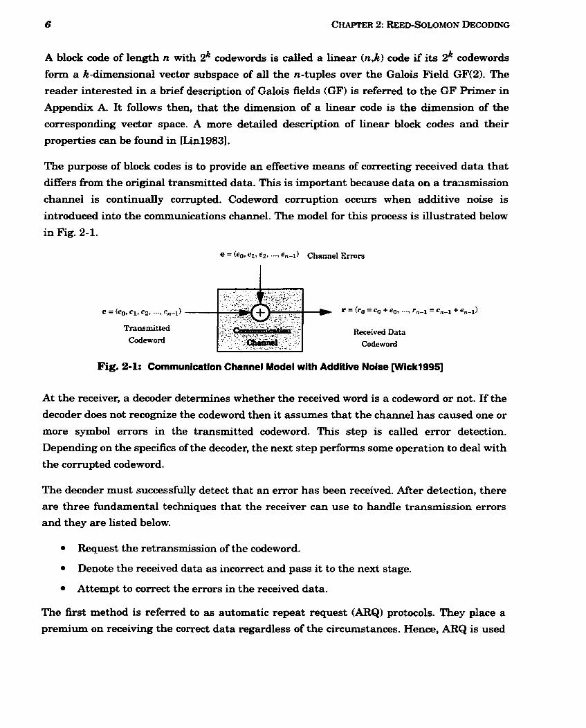
introduced into the communications channel. The mode1 for this process is illustrated below
in Fig. 2-1.
Trammitted
Codeword Received Data
Codeword
Fig. 2-1: Communication Channel Model with Additive Noise [Wick1995]
At the receiver, a decoder determines whether the received word is a codeword or not. If the
decoder does not recognize the codeword then it assumes that the channel has caused one or
more symbol errors in the transmitted codeword. This step is called error detection.
Depending on the specifics of the decoder, the next step performs some operation to deal with
the corrupted codeword.
The decoder must successfully detect that an error has been received. After detection, there
are three fundamental techniques that the receiver can use to handle transmission errors
and they are listed below.
Rques t the retransmission of the codeword.
Denote the received data as incorrect cuid pass it to the next stage.
Attempt to correct the errors in the received data.
The first method is referred to as automatic repeat request (ARQ) protocols. Tbey place a
premium on receiving the correct data regardless of the circumstances. Hence, ARQ is used
where an extremely low bit-error rate (BER) is demmded. It can be extremely slow if there
are numerous errors at the receiver. The next option is used in situations that require a high
throughput rate. When the decoder receives and detects the data error, it will flag the data
as king incorrect. This data is passed to the next stage, but it is marked as being an error. A
hi& BER must be tolerated in this case since there is no attempt at correcting the error. The
last method is known as forward error correction (FEC). FEC systems determine the validity
of the received data and can correct it based on the arithmetic or algebraic structure of the
code. RS codes are a type of FEC method.
2 . . Forward Error Correction
There are several characteristics of FEC codes that need to be discussed before the concept
of RS decoders can be described. First, if the decoder accepts the received word as being
valid, but it is a codeword different from the one that was initially transmitted then this is
known as an undetectable error pattern. This occurs when the channel inundates the data
with an inordinate amount of errors; thereby changing the original codeword into a
completely different but valid codeword. Recognizing the word as being a valid codeword, the
decoder assumes it to be correct and does not attempt to correct it. If there are a total of M
codewords then there will be (M - 1) such undetectable error patterns.
Second, one of the inherent limitations of FEC is that it is possible for the decoder to commit
a decoding error. This occurs when the decoder recognizes that the received word is in error,
but it incorrectly selects a codeword other than the one which was transmitted.
Unfortunately, if this occurs it is impossible for the decoder to indicate that it has failed to
correct the word. This phenornenon typically occurs when the number of errors in the
codeword exceeds the error correcting capability of the decoder (i.e., it exceeds the distance
properties of the code).
To characterize the error correction capabilities of FEC block codes, a few concepts must first
be defined. The number of nonzero positions in a codeword or error pattern is called its
weight. In addition, the Harnrning distance between two symbols of a word is the number of
coordinates or bit positions in which the two blocks differ. The shortest Hamming distance
between al1 distinct pairs of codewords in a block code C, is the minimum distance of the
code. This is sigdcant because a code with a minimum distance d,, can detect al1 error
patterns of weight less than or equal to (d,, - 1). Although it is important to detect errors.
the main function of the FEC decoder is to correct received error patterns. Therefore, a code
with a minimum distance d& can correct all error patterns of weight less than or equal to
L(d,,, - 1)/2 J . This equation represents the upper bound on the weight for which one can
correct all error patterns. I t is possible, but highly improbable, that one more error than
given by the upper error bound can be corrected in certain received blocks.
Finally, FEC decoders are susceptible to committing a decoder failure, which are completely
detectable unlike decoder errors. Let a tsrror correcting decoder receive a word r. The
decoder then tries to select a codeword c that minimizes the distance between the two. A
decoder failure occurs when no such c exists that satisfies the following:
minimum distance between (c, r) 5 t . Nevertheless, detecting the failure for RS codes is not trivial especidly in hardware
implementations of the decoder. It involves testing a polynomial generated by the decoding
algorithm to ensure that there are no repeated roots.
Using the preceding discussion as a basis, it now becomes possible to fully elaborate on
Reed-Solomon codes, which is one of the fundamental topics of this thesis.
2.1.2 Reed-Solomon Codes
Reed-Solomon codes are special types of FEC block codes. They are based on the same
fundamentals as other block codes. However, RS codes are an extremely powerfd set of error
correcting codes that are based on symbols rather than on bits. The general structure of an
RS code can be described as follows. Each code is composed of n symbols with a certain
number of message symbols k and redundant symbols (n - k). The code is referred to as an
(n,k) Reed-Solomon code of length n, and dimension k over a Galois field GF(q), where q is
the power of a prime number q = pm. It has a minimum distance of d, where d = n - k + 1 and
n = q - 1, and an error correction capability of t = (n - k)/2 errors.
Codewords are generated by a set of polynomials with degree k - 1 and coefficients from
GF(q). Al1 of the RS codes that are relevant to digital communications are based on the
binary extension field GF(2m), where each symbol is an m-bit word. Conveniently, if m = 8
then each symbol is an 8-bit word or byte, which is suitable for applications of digital
communications. RS codes are also defined to be maximum-distance separable (MDS) codes,
which means they satisfy with equality an axiom known as the Singleton bound dmi, I n - k + 1 . Thus, their minimum distance is always one more than the number of
redundant symbols [Cos t 19981.
RS codes me suited for communication channels that are susceptible to burst errors. To
elaborate, the RS decoder operates on symbols rather than on individual bits of the data
stream. Therefore, the decoder corrects the entire received rn-bit symbol regardless if there
is one bit error or rn-bit errors caused by a burst noise error event. Conversely, if there are a
srnattering of bit errors throughout the code word, then the decoder's resources are not being
put to optimal usage. In perspective, the bit-error correcting capability can thus range from
rn bits (bit errors are dispersed) to rn2 bits (the bit errors are contiguous).
Furthemore, the use of erasures enhances the error correcting capability of an RS code.
Erasures provide the decoder with more information about the errors in the codeword. An
erasure location is a symbol location in the codeword, which the decoder recognizes as being
incorrect. Howerer, the decoder does not know which bits are in error or what the correct
syrnbol is. This differs fkom an error in that the decoder does not know where or what
magnitude the error is when it receives a corrupted codeword. Since erasures provide
additional information, they increase the error correcting capability of a code. If there are v
erased coordinates then it is possible to correct t = (Ld,,, - v - 1 J)/2 errors in the unerased
coordinates of the received word. Hence, the decoder can correct e errors and u erasures as
long as (2r -; v ) < clmi, . A decoder is thus able to correct twice as many erasures as errors
becauae of the additionai location information.
The applicability of RS codes is greatly augmented through the use of linear code modifiers.
There are several implementations where extemal constraints determine the allowed length
of the error control code. If the original code construction is not suitable for a particular
application, then the code may be altered without changing its basic functionality. These
slight codeword deviations are punctwlng, extending, shortening, lengthening, expurgating
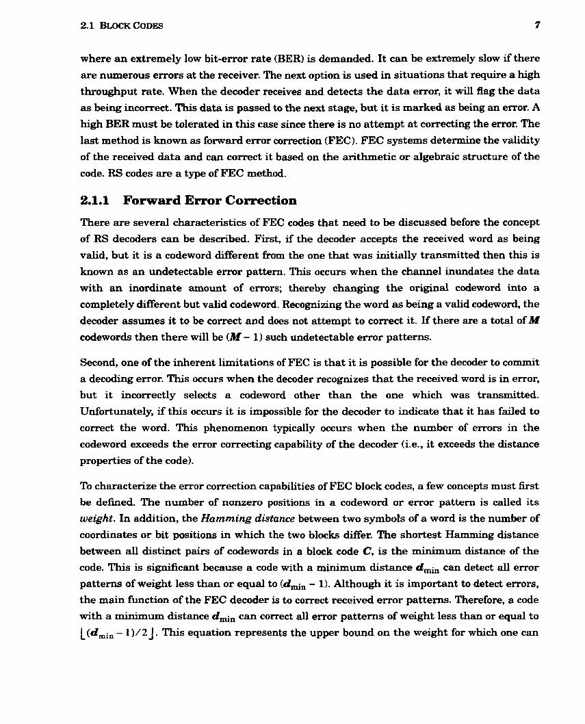
and augmenting. The effects on the original (n,k) code are siimmarized in Table 2-1.
'Igble 2-1: RS Code Modifiers 1
Explanation
x parity coordinate(s) deleted
Add x redundant coordinate(s)
x message coordinate(s) deleted from the encoding process
Add x message coordinate(s)
x code word(s) deleted
x new code word(s) added
Modification
, Puncturing
Extending
Shortening
Lengthening
Expurgating
Augmenting
New Form of (n, k) Code
(n - x, k)
(n + x, k )
(n - x, k - X)
(n + x , k +XI
(n, k -XI
(n, k +XI
To illustrate, digital video broadcasting (DVB) is based on a (255,239) RS code with a
primitive polynomial m ( x ) = x8 + x4 + x3 + x2 + I [Sohi2000]. However, in order to form the
actual code that is used by DVB, the original RS code is shortened by x = 51 symbols
resulting in a (204,188) code. The use of these modifiers is quite pervasive and they are
found in a myriad of applications. This will become apparent in Section 2.1.3, which
discusses the areas that use RS codes.
Time-Domain and kequency-Domain Interpretations in GFs
As previously stated, Reed-Solomon codes can either be decoded using a tirne-domain (TD) or a eequency-domain (FD) approach. Therefore a succinct discussion now follows, which
relates the FD to the TD in the context of GF arithmetic. This serves to facilitate the
understanding of the two RS decohg approaches.
If c is a vector over GF(q) then it is related to its transform C by the following equations:
where the character a is a primitive element in GF(2m) (see Appendix A for a detailed
description). The preceding transforrn is a generalization of the discrete Fourier transform
(DFT) to finite fields. Hence, the same properties of the DFT are tme for the Galois field
Fourier transform (GFFT) in Equation 2-1. A few example properties are linearity, shifting
and convolution.
Codewords are generally transmitted as a sequence of symbols indexed in tirne. Therefore,
the GFFT is a convenient method for translating TD characteristics into FD characteristics.
The FD equivalent or spectrum of the TD polynomial ch) = co + c p + ... + ~,-~x"-l is the
GFFT of the vector c = (co, cl, ..., c ~ - ~ ) . From this relation, two more theorems can be
defined. First, d is considered a zero of the polynomial c(x) if and only û the jth frequency
component of the spectrum of c(x) equals zero Wick19951. Conversely, a J is a zero of the
polynomial C(x) if and only if the i& time component ci of the inverse transform c of C equals
zero. These principles can be applied to RS codes in order to achieve FD decoding. A full
explanation of the implementation of the FD and TD decoders is presented in Chapter 3.
2.1.3 Applications
RS decoders can be found in a wide array of applications. Mthough the majority of RS decoder applications have k e n in the last decade or so, implementations which used the
code became apparent shortly afker their discovery in the early 1960's.
One of the first areas to use RS codes as a means of error correction was deep-space
communication in the early 1970s Wick19941. The Mariner Mars orbiter mission in 1971
used a (6,4) RS code over ~ ~ ( 2 9 . However, it could be argued that this was not really a true
implementation of the code, but rather ody a very special case. The code had a redundancy
of two so it could only correct one error. Hence, it was more aptly called a generalized
Hamming code. It was not until1977 that the Voyager mission made full use of the powerful
error correcting abilities of RS codes. The spacecraft was fitted with a concatenated 8 4 3 2 (255,233) RS code with a primitive polynomial m(x) = x + x + x + x + 1. In a concatenated
system, an inner and outer decoder are used in conjunction with one another. The inner
decoder is set adjacent to the noisy communication channel and it occasiondy makes errors
that tend to be bursty and hard-quantized. These are exactly the types of errors that an
outer RS decoder is proficient a t correcting.
The most recent standard Wick19941 on RS codes for deep-space applications was set out in
1984 by the Consultative Committee for Space Data Systems (CCSDS). It has been adopted
for use in several planetary and deep-space missions. The standard is a (255,223) RS code
over GF(~') and is represented by the polynomial m(x) = x8 + x7 + x2 + x + 1. Therefore, the
search for more efficient RS decoding implementations is reinforced by the continued
exploration of the depths of the universe.
Probably the most widely known application of RS codes is the CD player. What is
interesting here is that it makes use of RS code modifiers. It uses two shortened RS codes
with &bit symbols taken fkom ~ ~ ( 2 ' 1 . The two codes are cross-interleaved together with the
first code being a (32,28) code and the second a (28,241 code.
In addition, the digital versatile disc (DVD) standard is based on a (255,239) RS code with
symbols h m ~ ~ ( 2 ~ 1 and primitive polynomial m(x) = x8 + x4 + x3 + x2 + 1. It makes use of
the code modifiers in an innovative row-column configuration. The column RS-code is
shortened by 47 symbols to form a (208,192) code. Next, the row RS-code is shortened by 67
symbols and punctured by 6 symbols resulting in a (182,172) code.
DVB has three standards that use identical RS code parameters, which were first described
in Section 2.1.2. These are satellite (DVB-S), cable (DVB-C) and terrestrial (DVB-T) transmission. The most widely used of the three protocols is DVB-S [Sohi20001.
The two applications that are targeted in this thesis are G.lite (ADSL) and powerline
communications. Both standards use a (255,239) RS code, have an error correcthg 8 4 3 ' capability of t = 8, and are based on the primitive polynomial m(x) = x + x + x + x' + 1. A
maximum decoding speed of 20 MBps is required for these applications. This speed
comfortably accommodates G.lite (1 MBps) [ITU1999], very-high-speed digital subscriber
line (VDSL) (13 MBps) [Coop2000], and powerline communications (13.75 MBps). The
reasons for choosing these standards are three-fold. First, these code parameters are one of
the most widely used RS codes to date. If the research focus of this thesis is targeted to these
RS codes, then the results will be applicable to a greater number of applications. Second, the
RS code parameters are amenable to VLSI design. The codeword symbols are 8-bits or one
byte and the primitive polynomial facilitates the design of GF arithmetic circuits. Finally, these standards are both applicable to the concept of home networking, which is rapidly
increasing in popularity
However, the Data-Over-Cable Service Interface Specification (DOCSIS) standard could be a
possible target of this thesis as well. DOCSIS, popularly known as a cable modem, has a
variable error correction capability in the standard, which ranges from t = 1 to t = 10 errors.
If t = 8, then the DOCSIS RS specifications would be identical to those of powerline
communications and G.lite. Other applications where RS codes are used include cornputer
memory, wideband code division multiple access (WCDMA), and magnetic dis k storage.
Table 2-2 provides a summary of some of the more relevant applications that use RS codes.
The numerous applications serve to reidorce that there is a need for conducting research
into the area of RS codes and RS decoders. Nevertheless, the difficulty in choosing the
appropriate RS code lies with the development of an efficient, but yet simple decoding
algorithm.

able 2-2: Applications and their Corresponding RS Code Specifications
I I RS Code Specification
(n, k) -- --
Shortened & Cross- Interleaved Dual Code
(32,281 & (28,241
Application Primitive Polynomial
Column - Shortened (208,192)
Row - Shortened & Punctured (182,172)
DVD [SohiZOOO]
Shortened (204,188)
8 4 3 ' m(x) = x + x +x +x'+ 1
DOCSIS [RF119991
8 4 3 2 m(x) = x +x + x + x + 1
CCSDS [Wick1994]
Varies (144,128) or (240,224). Other (n,k)
are possible but n 1 255.
8 7 2 m(x) = x + x + x + x + 1
Powerline Communications
1
a. Ranges depend on the desired size of the error correcting capability of the codes t , which can range from r = 1 tor= 10.
m(x) = x + x + x + x + 1 8 4 3 2 1
2.2 Reed-Solomon Decoding Algorithms
The most challenging aspect of RS codes is finding efficient techniques for decoding the
received symbols. There are several problematic issues that arise with decoding RS codes.
For instance, how to minimize the occurrence of undetectable errors and how to reduce the
number of decoder failures, which were both explained in Section 2.1.
Research in this area has led to the development of a few relatively reliable decoding
dgorithms. This section succinctly discusses ihese algorithms. Hence, the goal here is to
provide the reader with a basic understanding of the mathematical steps each algorithm
requires, rather than a theoretical in-depth explanation. The reader who is interested in the
latter is directed to mick19941 and [Wick1995].
Before the ensuing discussion, some concepts are required to be defined for some of the
algorithms. First, let the error vector be e = (e,, e ,, . . .en -, ) , which has a polynomial
representation
If the original encoded codeword is c and it has a correspondhg polynomial ch) , then the
received polynomial a t the decoder is
This polynomial can be evaluated a t a, a2, ..., aP, which are the roots of the generator
polpomial g(x). Therefore, a set of 2t equations must be solved in order to obtain what are
known as the syndromes Sk, k = 1,2, ..., 2t where
The syndrome polynomial can then be defined as
where Si are the syndromes from Equation 2-5. Furthemore, let there be v errors, at u
iinknown error location numbers XI, X2, ..., X, with v unknown error values Yi, Yz, ..., Y, An error evaluator polynomial is related to the error locations and error values as follows:
Now define the error locator polynomial Ab), to be
A ( x ) = I +A,x+ ... + A u x u . (2-8)
This polynomial has as its roots the inverse error location numbers X;', for 2 = 1,2, ..., o. So
AU of the preceding polynomials can be related by means of a key equation defined as
Therefore, it is the function of the decoding algorithm to solve the key equation for Nx). In
FD decoding, the same key equation is used, but there is a different interpretation of the
results. Hence, its subsequent treatment is quite different. This will be M y elaborated on in
Chapter 3.
2.2.1 Berlekamp-Massey Algorithm
The Berlekamp-Massey (BM) algorithm is an efficient method used for correcting a large
number of errors. Its complexity increases linearly, which allows for the constmction of
efficient decoders.
A linear feedback shift register (LFSR) can be used to find A(x), where the coefficients of A(x)
are taken to be the taps of the LFSR. The algorithm uses five parameters: a length k LFSR
A(~)(X), the correction polynomial nx) , the discrepancy A ( ~ ) , the length L of the shiR register,
and an indexing variable K. The decoding process [Wickl995] is as follows:
(i) Cornpute the syndromes &, S I , .. ., S2 for the received word.
(ii) BM algorithm initialization is: k = O, d0)(x) = 1, L = 0, and Th) = x.
(iü) Set k = k + 1. Then calculate the discrepancy by subtracting the kth output of the LFSR defined by - ')(x) from the kth syndrome as follows:
(iv) 1f A ( ~ ) = O, then go to (viii).
(vi) If 2L 1 k , then go to (viii).
(vii) Else set L = k - L and T(x) = - "(x) / then go to (viii).
( v 3 Set T(x) = x * n x ) .
(ix) Ifk > Zt, thengo to (iii).
(x) Else if roots are NOT distinct then go to (xii).
Else (as part if statement in step (ix)) roots are distinct so determine the mots of A(%) = A(?x) by fmding the error magnitudes which are defined as
Correct the corresponding locations in the received word by adding the corresponding error magnitude and STOP.
Declare a decoder failure and STOP.
This concludes the explanation of the BM decoding algorithm.
2.2.2 Modified Euclidean Algorithm
The Modified Euclidean Algorithm (MEA) is based on the Euclidean algorithm, which
iteratively finds the greatest common divisor (GCD) of two elements in a Euclidean domain.
Mathematically, the original Euclidean algorithm proceeds as follows:
(i) Define two Euclidean elements (a,b) and the initial conditions: r-l= a , ro= b, s-l= 1, s0= 0, t-l= O and to= 1.
(ii) Recursively compute si, 4, and ri (while ri < r i - l ) as follows:
At any given time in the algorithm, the recursion relations in (ii) guarantee that the relation
sia + tib = ri is tme. This relation corresponds to the key equation stated in Equation 2-10.
However, the original Euclidean algorithm is not suitable for RS VLSI design because each
iteration requires a division to be computed [Shao1985]. Finite-field inverses are used in the
division calculation. Unfortunately, they are area intensive operations. The original
algorithm can be modified though to eliminate the computation of inverses during the
iterations, which in turn reduces the hardware complexity. This modification makes the
MEA comparable to the BM algorithm in terms of VLSI implementation feasibility
[Wick1995]. The benefit of the MEA though is its low complexity and simplicity with which it
is understood and applied. Furthermore because of its structure, the MEA finds both the
error locator and the error evaluator polynomials.
Consequently for practical reasons, the MEA rather than the original algorithm is used for
decoding the key equation. AU implementations that are based on Euclid's GCD algorithm
use the modified version. Thus, a thorough presentation of the MEA will be provided in
Sedion 3.5 of Chapter 3, and the original version will not be discussed further in this thesis.
The reader who would like a more detailed explanation of the Euclidean algorithm in terms
of RS decoding is referred to [Wick1995].
The MEA was chosen to be the decoding algorithm for this thesis. Hence, a cornprehensive
discussion of the MEA is deferred to the next chapter in Section 3.5. A greater emphasis will
be placed on the MEA as opposed to the BM algorithm. The reasons for choosing the MEA
are as follows. First, it can be argued that both algorithms are comparable in terms of
efficiency. However, the MEA is conceptudly easier to understand and stmcturally less
cornplex. This translates into less design tirne, which is crucial in meeting today's intense
time-to-market demands. Second, there were more architectural enhancements suggested
for the MEA than for the BM algorithm such as those found in [Shao1985], lHsTr19881,
[Kwon1997] and [Ohl997]. By examining certain key designs, it was ascertained that the
MEA codd be modified so that it was applicable to the targets of this thesis. Various blocks
of the MEA were found to be structured in such a way as to minimize area and reduce power
consumption. In addition, finding an implementation that was optimal in terms of silicon
area was integral to this thesis. GF multiplication and division are two arithmetic
operations that are area intensive. Therefore, it became imperative to use the MEA
implementation, which reduced the number of GF operations used in the decoder's iterative
procedure.
Finally, after reviewing previous implementations, it became apparent that the MEA was
used more often [Shao1985], [ShTr1985], fHsTr19881, [Shao1988], [Truo19881, Wh1t19911,
[Chen1995], [Jeon1995], [Kwon1997], [Ohl997], [Jenn1998], Wilh19991 and Buan19991
than the BM algorithm [Reed1991], Wsu19961, [Ragh1997], mtz19981, [Jeng1999] and
[ChanZOOl]. Research that uses the MEA and offers a definitive qualitative and quantitative
cornparison would thus be of greater value to the field of RS decoders. In short, it is believed
that the MEA provides the most optimal decoder architecture that focuses on the goals of
this thesis.
2.2.3 Other Decoding Algorithms
The MEA and the BM algorithm are the two decoding approaches found most fkequently in
applications using RS decoders. They are straightforward to understand and their
structures are suitable for VLSI design. However, research is being conducted into more

abstract, but efficient methods of RS decoding. These are the areas of soft-decision decoding
and remainder-based decoding. A brief discussion of these methods is included for
thoroughness.
Remainder-based decoding does not require the computation of the syndromes from
Equation 2-5. Instead the algorithm uses a remainder polyno~nial r(x), which is obtained
from the division of the received polynomial u(x) by the generator polynomial g(x), as
r ( x ) = r O + r l x + ... + r n - k - l p z - k - 1
r(x) = U ( X ) mod g(x).
The algorithm was developed by Welch and Berlekamp and is aptly narned the Welsh-
Berlekamp (WB) algorithm. In terms of hardware realization, there is no circuitry required
for syndrome calculation. The WB algorithm involves the use of four polynomials instead of
the usual two found in either the MEA or the BM algorithm Wick19941. Therefore,
additional registers, multipliers and adders are needed for the decoder block. Nevertheless,
the algorithm can be implemented using systolic arrays and is similar in complexity to both
the BM algorithm and the MEA [Dabi1995]. This thesis did not consider implementing a WB
algorithm because of the lack of existing practical applications that use this approach. The
reader is referred to [Ber11986], [Wick1994] and [Dabi1995] for a more engaged description
of the algorithm and the associated architecture.
Each of the algorithms discussed thus far can be classified as being a hard-decision decoder
(HDD). The detection circuit requires that its inputs be fi-om the same symbol alphabet as
the channel input [Wick1994]. However in certain instances, the received signal may not
offer a clear choice as to which of the possible s p b o l s has been transmitted. The receiver
then must guess as to which of the symbols the received value most closely resembles. On
the other hand, a sofk-decision decoder !SDD) accepts an actual vector of noisy channel
output samples and estimates the vector of channel input symbols that was transmitted.
Unlike the HDD, the SDD does not force a decision which is likely to be incorrect. Therefore,
SDDs can provide a coding gain of about 2dB more than that provided by HDDs.
The decoder can be supplied with soft-decision data quite readily, but the difficulty is
obtaining an optimal SDD that is not prohibitively cornplex. Current algorithms are non-
algebraic and run in time that scales exponentially with the length of the code. However, in
[KoetZOOO], a new algebraic soft-decision decoding technique is developed. Currently, the
research focus in this area is in devising an efficient decoding algorithm that c m be
practically implemented in VLSI applications.
2.3 Previous Reed-Solomon Decoder Implementations
The foundation for RS decoder VLSI research can be found in [Shao1985] where for the first
tirne, an efficient hardware implementation of an RS FDD was discussed. Before this
approach, the decoder design was extremely complicated and it occupied an prohibitively
large silicon area. To its credit, [Shao 19851 developed a regular pipelined architecture that
was suitable for VLSI design. Nevertheless, there was no mention of fabricated silicon. Thus,
no predefined benchmark was provided for other researchers in this area to compare their
work against. In addition, the technique did not incorporate erasure correction into the
decoder. The ability of an RS decoder to support erasures dramatically improves the
correction capability of the decoder.
Subsequent to [Shao1985], the same authors reported an actual silicon implementation in
fShTr19851. Several modifications were made such as including erasures, and performing
tirne-domain based decoding. In addition, the TDD was stated as being superior because it
was simpler, more regular, had less area and operated equally as fast as the FDD in
[Shao1985]. However, there were no specifics aven about the actual area which was saved or
the speed of operation of either decoder. The statement about the TDD having a more
regular structure was incorrect as well. One of the apparent advantages, if ans of the FDD
over the TDD is that its structure is simple, repetitive, and therefore less complex than the
TDD.
Following this groundbreaking work, a comparison between the two decoding methods is
made in MsTr19881. Hardware architectures are illustrated for both methods and the
design of each approach is clearly shown. AU stages of the decoder are compared and
contrasted using both methodologies. The FDD is lauded as being superior to the TDD
because the FDD is stated as being considerably less complex. Moreover, the only apparent
trade-off is that the FDD occupies a larger silicon area, but for most of the codes in use today
the extra area is insignificant. However, stating that an FDD is less complex than a TDD
gives no substantiated information on the performance of the decoder. No numbers are
provided for how much larger an area the FDD occupies or how fast each of the decoders
opergte. In fact, there is no mention of any results &om silicon. So although [HsTr1988]
established some preliminary distinctions between the two decoding approaches, no
definitive results were published.
Finally [Shao1988] elucidated the comparison of chip area that each decoder required,
through the use of a comparison table. Various decoder stages from each implementation
were compared based on the area that a polynomial multiplication circuit used. It showed

for the first tirne that the FDD occupied prohibitively more area than its time domain
counterpart. In fact, the TDD was extolled for having lower area, lower power consumption,
higher reliability and higher yield [Shao1988], ail of which lead to lower costs. Arnbiguity
nevertheless obfuscates the definitiveness of the results. For example, multiplier m a was
stated as king the unit of comparison for area. However, there was no mention of the exact
area or speed of the multiplier. This approach fadeci to show a meriningful analogy because it
lacked any tangible results f?om a fabricated chip. In short, an ameliorated view of the TDD
and FDD was brought to light, but [Shao1988] failed to provide unambiguous evidence to
support their claims. The TDD implementation was reiterated in [Truo1988] with no new
information.
Nevertheless, the publications previously discussed were the inflection point for an
exponential growth in RS decoder research. There were extensive research contributions to
this area over the past decade and they are referenced in the ensuing discussion. However,
al1 of them have failed to produce a definitive statement that is quantitatively supported.
[Reed1991] designed a VLSI RS decoder using an inverse-free Berlekamp-Massey algorithm.
The stated benefits of this algorithm were that it was less complex than the Euclidean
algorithm. However, again there was no accompanying VLSI support for this statement.
Although the algorithm managed to eliminate an area intensive inverse calculation, it used
a significantly large number of multipliers. No hardware results were provided.
VLSI results were reported in [Whit1991] for an RS tirne-domain codec. This
implementation used the MEA and was based on a (167,147) shortened RS code. The chip
contained 200 000 transistors, had an area of 68.88mm2, operated at a data rate of 80 Mbps,
consumed 500mW of power and was fabricated in a 1.6pm CMOS process. Erasures were
supported and it could correct up to and including t = 10 errors. This chip was strictly
targeted to advanced television and several limitations existed. First, the design was done
using a full-custom process. Thus, it had a high degree of complexity and the design time
was sigdcant. Today's intense tirne-to-market demands however require designs to be
expeditious. Second, large memory buffers were used extensively, which contributed to the
high silicon area. Next, the reasoning as to why the TDD approach was chosen was that it
could be implemented as a small array of identical cells. This statement could be said about
the FDD as well. Finally, this design could not be used as a pure decoder benchmark since it
incorporated the encoder design as well.
[Cho019921 discussed a VLSI architecture and offered a comparison between the TDD and
the FDD. No hardware was produced and the designs did not include any erasure handling
capability. The discussion is strictly based on the algebra behind the decoding and can use
either the MEA or the BM algorithm for decoding. In addition, the proposed algorithm used
more multipliers than several known implementations. There were several key comparisons
stated in this paper, and they are discussed shortly. Keep in mind however, that these
comparisons were assumptions based on the theory of the algorithm. No tangible results
were given because there was no accompanying silicon. First, the TDD algorithm was said to
require twice as many multiplications as the FDD algorithm. Thus, the TDD would not be
suitable for high-speed applications (> 200 Mbps), which require numerous multipliers.
However, for medium speed applications, the TDD would be superior because the
architecture would then be more dependent upon other criteria. These include regularity,
control complexity and flexibility. In addition, the time domain algorithm was lauded
because it could be implemented as a regdar amay of identical cells. However, this was
known to be tme for the FDD as well. Finally, the TDD is deemed to be better suited for
decoding truncated RS codes. In short, numerous comparative statements were made about
the two approaches to RS decoding, but they were all based exclusively on the mathematics
of the algorithm. A hardware implementation would have provided a truly conclusive
cornparison.
[Chi19931 designed an RS decoder which eliminated the Chien search block in order to
achieve a higher speed. The Chien search block was replaced by a redesigned block of
hardware that was faster. However, this new block occupied a larger silicon area as
compared to the Chien search block. In addition, the decoding algorithm was modified to
accommodate this new approach. Unfortunately, it was slower than both the MEA and the
BM algorithm. Overall, the decoder was stated as being faster, but this was at the expense of
an increase in area. No hardware was actually produced in this implementation either.
The design in [Chen19951 used a modified Euclidean algorithm (MEA) for the decoder. This
design was developed and tested with Verilog, which is a hardware description language
(HDL). However, no specific numbers from either software or hardware were mentioned. In
addition, the circuit used an area intensive read-only-memory (ROM) to store all the
required inverses.
[Jeon19951 presented what is probably the best comparison to date of the TDD and FDD. However, the goal here was to accomplish this juxtaposition without fabricating any
hardware. It used a variation of Euclid's GCD algorithm for solving the key equation.
Comparisons were made using a dependency graph (DG) and an entirely mathematical
approach. These comparisons were based on derived dependency structures in terms of total
computation (DG size) and critical path delay. It presented a good o v e ~ e w on RS decoders,
which could be used as a preliminary estimate before doing the actual hardware design. It
showed that the TDD is superior to the FDD in terms of delay and area. This was done
strictly in C-programming software and no HDLs were used. However, there were some
conspicuous limitations. Most importantly, the approach did not provide a method for
reporting power dissipation for either decoder. This is oRen the single most significant factor
in determining the feasibility and efficiency of a VLSI design. In addition, adding to the
complexity and ambiguity of the estirnates were the numerous factors that had to be
considered for the study. These included choosing appropriate mathematical strategies,
types of multipliers and dividers, and finite-field polynomials. Not al1 of these factors were
fully specified in the discussion.
An algebraic comparison of a Euclidean based algorithm and a Berlekarnp-Massey
algorithm was presented in [Saka1995]. Although no silicon was produced in this
publication, a prominent conclusion was stated. The results provided a proof of the
equivalence between the Berlekamp-Massey algorithm and the Euclidean algorithm in the
sense that both methods yielded distinct but similar paralle1 architectures with the same
optimal complexity.
In [Hsu1996], an RS decoder based on the Berlekamp-Massey algorithm was designed. No
hardware was fabricated but it was assumed, based on several coarse estimations, that the
design would have 406 000 transistors for a t = 8 error correcting code. The area was
significant because of several multipliers that were used in repeated cells in the decoding
algorithm. No other tangible specifications were mentioned.
[Ragh1997] developed a low power RS decoder design that was targeted towards portable
wireless receivers. However, it had double the area of traditional RS decoder
implementations and achieved a speed that was clearly in excess of what the target
applications required. The chip was still in the stages of testing and was not fabricated at
the time of publication. It used the Berlekamp-Massey decoding algorithm and it was
synthesized using a 2pm library. Estimated numbers from the design showed a bit rate of
343Mbps with 13945 gates. However, in order to achieve the lower power of the design the
preceding bit rate had to be rduced.
[Kwon1997] designed a combined RS decodedencoder for digital VCRs using a modified
Euclidean algorithm. This approach combined the encoder with the decoder in order to Save
hardware. Therefore, [Kwon19971 cannot be used as a benchmark for comparing other
decoders. No silicon was fabricated and the results were based on approximations deduced
solely from the algorithm. This proposed method included eraswe hanclhg, used 35 000
gates and targeted a speed of l8MHz. An important feature was its superior implementation
of the Chien search for saving area at the expense of speed. The design combined two large
computational blocks that are usually implemented separately. Although this lowered the
speed of the search block, it optimizd the area occupied by this traditiondy large block.
The reduction in speed should not bc an issue for meeting the design parameters of the
target applications in this thesis. Thus, this approach was used for the VLSI implementation
of the Chien search block in the TDD designed in this thesis.
[Oh19971 designed a similar RS decoder structure to that in [Truo1988]. The design
implemented a (207,187) RS code on an field-programmable gate array (FPGA) that had an
equivalent gate count of 50 O00 and a decoding speed of 10 Mbps. Target applications for this
decoder were DVDs and high definition television (HDTV). A comparison between the
proposed architecture and the one developed in [Truo1988] was made. There were some
interesting improvements that were applicable to this thesis. First, the overall decoder
complexity was reduced by about 30% to that found in [Truo1988]. Complexity in this case,
referred to the irnplementation area. The reduction was achieved by changing the parallel
structure of the polynomial expansion block to a serial architecture to Save area at the
expense of speed. However, the Chien search and the MEA that were used had a greater
degree of complexity than the previous approach. Nevertheless, the idea developed in the
polynomial expansion block can be incorporated into this thesis. The decoding speed was too
slow for the targeted applications of this thesis though. It was also difficult to compare this
decoder with other hardware designs because it was implemented in an FPGA not as an
ASIC.
EFitz19981 developed an alternative to the traditional RS decoder algorithms called the
Fitzpatrick algorithm, and compared it to the Berlekamp-Massey algorithm. This comparison was strictly theoretical and offered no sigdicant information about a hardware
implementation. The Fitzpatrick algorithm was viewed as having a lower degree of
complexitx but it used 2t2 multipliers for the decoding process. Designs with significantly
fewer multipliers have been realized, including the ones in this thesis.
[Jenn1998] offered an area/power comparison of an RS decoder based on a Euclidean
algorithm and the Fitzpatrick algorithm. The latter algorithm was CO-devised by one of the
authors in [ Je~1998] . However, the algorithm was not amenable to VLSI design. It was
stated that to just find the error locator polynomial alone required at most 2t2
multiplications and 2t divisions. This wodd amount to a prohibitively large area. In fact,
[Jenn1998] showed that the area was almost double that found in a Euclidean based
algorithm. The large increase in area was accounted for by the large amount of code required
for the Fitzpatrick algorithm. Therefore, a higher degree of complexity can be said to be
associated with that algorithm. A meager improvement in power dissipation was realized,
but with significant trade-offs in area and control complexit~ The implementation was only
simulated in software and no fabrication of silicon was attempted. In addition, the
cornparisons were made with RS codes of code length n = 24 and n = 32. This coding scheme
is not applicable to many of today's implementations. The design did not incorporate erasure
handling either.
A VLSI chip with published resdts was discussed in [Chan19991 and [ChSul999], which
used the Euclidean algorithm for the decoder. The chip had a total of 31 000 gates, operated
a t 40 MHz in the worst case and was fabricated in a 0 . 6 ~ process. There were significant
limitations with this implementation though. A maximum of t = 6 errors could be corrected
and the highest RS code it could accommodate was (200,188). It used area intensive ROMs
as inverse lookup tables. However, it boasted a 16% improvement in hardware complexity
over a previous approach Wwon19971. The results do not refer to actual silicon area because
the references to which this design is compared against do not fabricate any hardware.
Finally, the chip's design was too focused on speed with little emphasis placed on area
optimization. The applications to which it is targeted, simply do not require decoding speeds
in excess of 40 MHz.
A highly efficient, but extremely complex design in terms of control complexity, timing and
layout was presented in Wilh19991. A time-domain Euclidean algorithm was used for the
decoder. The chip was not fabricated, but the results of the proposed design were estimated
from a 0.5pm technology. This design had a speed of 620 Mbps, an error correcting capability
of t = 8, and an area of 1.6mm2 using 43 000 transistors and additional memory. It was
estimated that the design could be scaled to operate at 1280 Mbps, which corresponded to an
area of 3.0mm2 with 120 000 transistors plus memory. The design was Ml-custom however,
with a high degree of control complexity. Therefore, time-to-market could be an issue. The
decoding speeds were also exceedingly high for most practical applications today.
[Huan1999] designed an RS decoder targeted at ADSL applications. No hardware was
produced and al1 performance parameters were estimated. This design operated at a bit-rate
of 48 Mbps, had a gate count of 43 987, and had an error correcting capability of t = 8.
However, the design did not incorporate the ability to handle erasures. Thus, there would be
an increase in the silicon area and degree of complexity if' this design was to be used in a
pradical ADSL application. The design was a TDD that was based on the Euclidean
dgonthm. There was no reasoning given as to why the design was chosen to be a TDD
instead of an FDD though.
[Jeng1999] presented an RS decoder that used an inverse-fkee Berlekamp-Massey
algorithm. The design was implemented in software using C++, but no hardware was
fabricated. A (255,239) RS code was used to illustrate the benefits of the algorithm. However,
it was shown that the pmposed structure used a total of 113 multipliers. This was quite a
large number for the given code parameters. In addition, a finite-field divider was still
required by the Chien search block. The decoding algorithm did not use division, but it is
possible to use the modified Euclidean algorithm without performing a division as well.
An RS decoder for DVDs, which used a Berlekamp-Massey decoding algorithm was
presented in [Chan1998], (ChSh19991 and [Chan2001]. A chip was fabricated in a 0 . 6 ~
CMOS process for this implementation. It had a total area of 4.22x3.64mm2, a core area of
2.90x2.88mm2, a gate count of -26 000, an operating speed of 33MHz, and a power
dissipation of 102mW. The contribution fkom this implementation was sigdcant. A serial
architecture which had only three finite-field multipliers was used to implement the
algorithm efficiently. However, the finite-field multipliers used in this design were not as
optimal as other implementations. In this design, the multiplier was constmcted from 73
XOR gates and 64 AND @es. However in [Solj1996], a multiplier for G F ( ~ ~ ) was formulated
which essentially used only 48 AND gates and 62 XOR gates. RS decoders use numerous
multipliers so the design in [Solj1996] was more suitable for the area sensitive design in this
thesis. In addition, [Chan1998], [ChSh1999] and [Chan20011 used an area intensive look-up
table for the inverse calculations required by the Chien search. However, [Solj19961
presented an area optimized inverter. When used in conjunction with the multiplier, it
offered a considerable savings in area over a look-up table. In short, this design offered an
efficient decoding algorithm design, but the finite-field mathematical structures were not
the most optimal in terms of area efficiency.
To complete this discussion, a few examples of commercial RS decoder implementations will
be presented. Radyne ComStream developed an RS Codec [Rady1999] that was DVB
compatible. It was based on a (204,188) code, with an error correcting capability of t = 8.
Furthemore, it supportcd data rates ranging from 4.8 kbps to 8.5 Mbps. This DVB compatible chip met al1 DVB specifications.
Texas Instruments developed a software approach [Texa2000] of an RS decoder using C code.
It used the BM algorithm and was based on a (204,188) RS code with t = 8. The entire
decoding process took 2180 machine cycles to complete. This s o h a r e was targeted to run on
the Texas Instruments' CM00 digital signal processor.
e-MDT Inc. markets a programmable RS codec [eMDT2000]. Its code length was variable
between n = 85 and n = 255. It was implemented in a 0.8pm technology, operated a t a speed
of 80 Mbps, and had an ermr correcting capability of t = 8. In addition, the encoder and
decoder operated independently for full duplex operation. It was encased in a 68 pin package
and used one clock cycle per byte of processing. The device is suitable for magnetic recording
systems and other high-performance storage media applications. It may be adapted to a
wide range of wireless applications as well.
LSI Logic has developed a DVB Quadrature Amplitude Modulation (QAM) Modulator
[LSIL20001 which used an RS decoder. The modulator can accommodate a (204,188) RS code
and it can correct up to t = 8 errors. These parameters sa t i se the DVB standard
specification.
Finally, Advanced Hardware Architectures (AHA), developed a 100 Mbps RS emor correction
device. It supports several programmable parameters including block size, error threshold,
number of check bytes, and order of output. In addition, it can be programmed to correct
from 1 to 10 error bytes or 20 erasure bytes per block. These block lengths are
programmable f?om 3 to 255 bytes. It was encased in a 44 pin package and its target
applications include HDTV, ADSL, high performance modems, and global positioning
systems. A single-phase clock synchronized al1 chip fiuictions.
Table 2-3 quantitatively summarizes the results from the literature to date. It illustrates the
conspicuous lack of implementation detail in published RS decoder research. In addition,
none of the publications mention or describe any details about indicating a decoder failure.
Al1 of the designs appear to be focused on the decoding algonthm and there was no mention
of how to indicate or detect a decoder failure. As can be seen from the ensuing table, there
are a srnattering of test results which do not provide definitive answers in terms of
comparing the TDD and the FDD in hardware. .Much of the published literature failed to
discuss several important design parameters. This can be seen by the numerous blank
entries found in the table.

Iiable 2-3: RS Decoder Implementation Literature Summary
Power hW)
~ o r m ~ Area (mm2) -
-
RS Code Parametersa Tran sist
& Domain ors
Line Ares Width (-2) (m)
Speed
(15.9) FDD EA
Eraswes EA ( 3 1 3 ) Both
Erasures EA (255,223) Both
Erasures EA (255,223) Both
rrruo19881 Ir- Erasures EA
(255,223) Both I ( n i ) TDD BM 1 C-code [Reedlgg 11
W t 19911
[Cho019921
[Chi 19931
[Chen19951
[Jeon19951
[Hsu19961
IKwon19971
[Oh 19971
Erasures EA 200 k Full ( 167,147) TDD Custom
t = 10
(nt) TDD NIA 1 C-code
Erasures 1 C-code
TDD EA I l t l l O
40 MHz clock e.g.
Verilog (Func- tional)
TDD & FDD EA n = 255
l l n - h l 3 0 e.g., k = 231
n = 255 TDD EA 226k to 5 1 t 1 1 0 1 546k
C-code e.g. =
150 848
- -
36 MHz dock
- -
Erasures TDD EA (14,9), (85,77),
(149,138)
-
35kgates including encoder
Erasure TDD (207,187) t = 10
EA
FLEXlOK 50 FPGA 50k gates
Table 2-3: RS Decoder lmplementation Literature Summary
0.18 and square the quotient. Then divide the area by this result to find the nomalized area in O. I8pm. Note however that the number of layers of metal were not factored into this calculation. c. The number of metal layers was not provided in the publication.
Reference
[Ra&19971
[Chan19981
Fitz1998)
[Jenn19981
[Chan19991 [ChSul9991
[Huan1999]
[Jeng1999]
[Wilh1999]
[ChSh1999] [Chan20011
a. Algorithm
2.4 Summary
To put the history of RS decoding in perspective, a succinct outline of the progression of RS
decoder research is presented in Fig. 2-2. It shows a timeline of when RS codes originated
and then the subsequent research contributions towards finding the most efficient decoding
approach. Furthemore, it also shows when each of the major decoding approaches was first
discovered.
b. Area normalized to a O. 18pm CMOS technology and was calculated as follows. Divide the line width by
RS Code Parametersa & Domain
(63,57) TDD t = 3 BM
(208,192) TDD t = 8 BM
(n k ) TDD BM
(24,20) & (32,26) TDDt=3
EA
(200,188),(60,40) (120,108),(40,28)
t = 6 E A
(255,k) TDD t = 8 E A
Er asures (255,239) TDD
t = 8 B M
Erasures (167,147) TDD
t=10EA
(208,192) & (182,172) TDD
t = 8 B M
used in decoder BM -
Transist ors
48 570, 13 945 gates
21910 gates
algorithm
-
-31k gates
43 987 ga tes
C++ Code
73 000
-26 000 gates
99 pins
Berlekamp-Massey
Power (mW)
-
-
-
280 (n J)
-
-
-
-
102 @3V
or EA -
Speed
343 Mbps
16.67 M H z clock
-
111 kHz clock
40 MHz clock
48 M ~ P S
-
256 M ~ P S
33 MHz clock
Eudidean
Line Width (Pm)
2 2LM
0.6 SPDM
-
-
0.6 2LM
-
-
---
0.5'
0.6 SPDM
Based Algorithm
(-2)
-
12.35
-
-
-
-
-
1.7
15.36
or NIA
~ o n a ~ Area (mm2)
-
1.11
-
-
-
-
-
0.612
1.38
Fig. 2-2: Reed-Solomon Decoder Outline and Timeline (FDD Indicated by Dashed Oval - - = )
Chapter 2 has shown that attempts thus far have failed to give palpable evidence of the
superiority of one RS decoder implementation over the other. This has served as the
motivational precedence for this thesis. To recapitulate the essential points of this chapter:
Reed-Solomon codes were described as a specific type of forward error correcting block
code.
The parameters and properties that d e h e an RS code were thoroughly presented.
Applications that use RS codes, encompassing the target applications of this thesis, were
presented. The widespread use of the RS decoder motivates the research behind this
thesis.
The various RS decoding algorithms were explained, including the rationale behind
choosing to implement the MEA in this thesis.
A literature review of previous implementation proposais was presented. It illustrated
the inherent lack of tangible evidence to support the VLSI implementation of either the
TDD or the FDD.
Consequently, a TDD and an FDD will be designed and fabricated in this thesis to finally provide an authoritative statement on each of the RS decoding approaches. The next chapter
describes the mathematics and structures associated with the RS TDD and FDD.

Chapter H Reed-Solomon Decoder Design
The general structure of RS codes and the algorithms used in decoding them were described
in Chapter 2. This chapter goes into further detail and explains the mathematics and
methodology involved in designing an RS decoder. The design of an RS decoder c m
essentially be divided into several distinct functions or blocks. It has a pipelined stmcture,
meaning that the received codeword moves through the various stages until it is decoded
and ready to be output. In addition, included in the description will be an explanation of
erasure handling. This adds some complexity to the decoder, but at the same time it provides
a greater error correcting capabdity. Nevertheless, erasures can be ornitted fxom the decoder
design if the specinc application does not require it. Before elaborating on each block though,
a brief o v e ~ e w of the general structure of both the TDD and the FDD will be given.
3.1 Implementation Overview
TDD and FDD designs are developed in [Shao1985], [Shao1988], and [HsTr1988], which
serve as the basis for this discussion. To begin, the RS code is constmcted from GF(Zm) with
2" elements. Each codeword has a length of n = 2m - 1 and a minimum distance d. The
nurnber of message symbols k, that are encoded can be expressed as k = n - (d - 1). This
forms an (n,k) RS code with k m-bit message symbols and (d - 1) parity symbols. Throughout
the rest of the discussion, the following five vectors will be used:
c = (cg, c l, . . . C, - ), codeword vector
r = (rO, rl , . . . rn - , ), received vector
e = (eo,el, ... en- ,), error vector
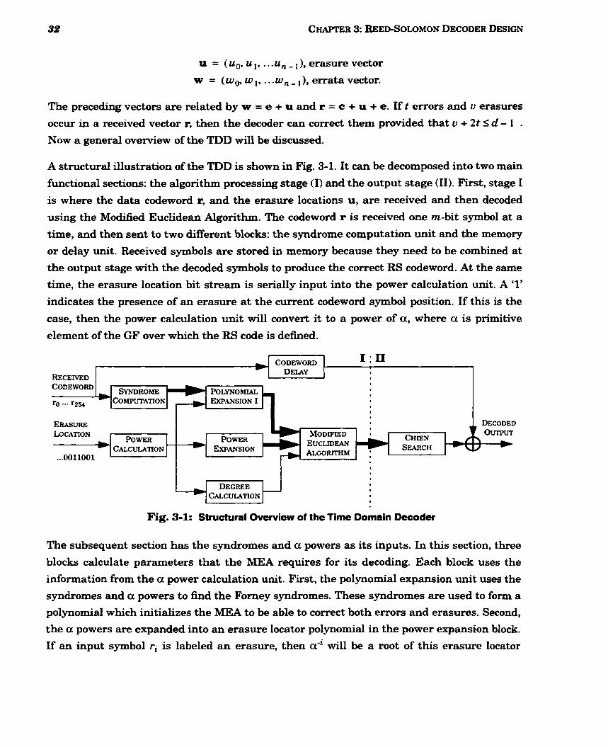
u = (u0, u,, ... u n _ ,), erasure vector
w = (w O, w , , . . . w , - , ), errata vector.
The preceding vectors are related by w = e + u and r = c + u + e. If t errors and v erasures
occur in a received vector r, then the decoder can correct them provided that v + 2 t I d - 1 . Now a general ovemiew of the TDD will be discussed.
A structural illustration of the TDD is shown in Fig. 3-1. It can be decomposed into two main
functional sections: the algorithm processing stage (1) and the output stage (II). First, stage 1 is where the data codeword r, and the erasure locations u, are received and then decoded
using the Modified Euclidean Algorithm. The codeword r is received one m-bit symbol at a
time, and then sent to two different blocks: the syndrome computation unit and the memory
or delay unit. Received symbols are stored in memory because they need to be combined at
the output stage with the decoded symbols to produce the correct RS codeword. At the same
tirne, the erasure location bit stream is serially input into the power calculation unit. A '1'
indicates the presence of an erasure at the current codeword symbol position. If this is the
case, then the power calculation unit will convert it to a power of a, where a is primitive
element of the GF over which the RS code is dehed .
Fig. 3-1: Structural Overview of the Time Domain Decoder
The subsequent section bas the syndromes and a powers as its inputs. In this section, three
blocks calculate parameters that the MEA requires for its decoding. Each block uses the
information fi'om the a power calculation unit. First, the polynomial expansion unit uses the
syndromes and a powers to find the Fomey syndromes. These syndromes are used to form a
polynomial which initializes the MEA to be able to correct both errors and erasures. Second,
the a powers are expanded into an erasure locator polynomial in the power expansion block.
If an input symbol ri is labeled an erasure, then a-' will be a root of this erasure locator
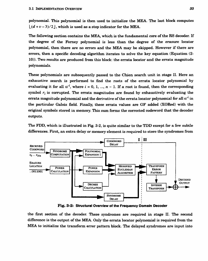
polynomial. This polynomial is then used to initialize the MEA. The last block computes
L(d + u - 3)/2 J , whieh is used as a stop indicator for the MEA.
The following section contains the MEA, which is the fùndamental core of the RS decoder. If
the degree of the Forney polynomial is less than the degree of the erasure locator
polynomial, then there are no errors and the MEA may be skipped. However if there are
errors, then a specific decoding algorithm iterates to solve the key equation (Equation (2-
10)). Two results are produced fkom this block.: the errata locator and the errata magnitude
polynomials.
These polynomials are subsequently passed to the Chien search unit in stage II. Here an
exhaustive search is performed to fbd the roots of the errata locator polynomial by
evaluating it for d l a-', where i = 0, 1, ..., n - 1. If a root is found, then the corresponding
symbol ri is compted. The errata magnitudes are found by exhaustively evaluating the
errata magnitude polynomial and the derivative of the errata locator polynomial for all a-' in
the particular Galois field. Finally, these errata values are GF added (XORed) with the
original symbols stored in memory. This sum forms the corrected codeword that the decoder
outputs.
The FDD, which is illustratecl in Fig. 3-2, is quite similar to the TDD except for a few subtle
differences. First, an extra delay or memory element is required to store the syndromes from
Fig. 3-2: Structural Overview of the Frequency Domain üecoder
the first section of the decoder. These syndromes are required in stage II. The second
difference is the output of the MEA. Only the errata locator polynomial is required from the
MEA to initialize the transform error pattern block. The delayed syndromes are input into
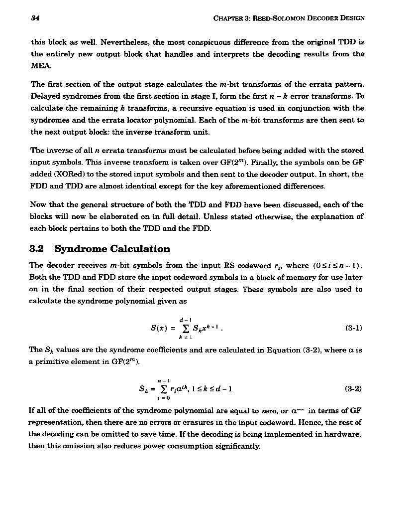
this block as well. Nevertheless, the most conspicuous difference fkom the original TDD is
the entirely new output block that handles and interprets the decoding results from the
MEA.
The fmst section of the output stage calculates the m-bit transfonns of the errata pattern.
Delayed syndromes from the f h t section in stage 1, form the flrst n - k error transforms. To
calculate the remaining k transforms, a recursive equation is used in conjunction with the
syndromes and the errata locator polynomial. Each of the n-bit transforms are then sent to
the next output block: the inverse transform unit.
The inverse of d n errata transforms must be calculated before being added with the stored
input symbols. This inverse transform is taken over GF(2m). Finally, the symbols can be GF
added (XORed) to the stored input symbols and then sent to the decoder output. In short, the
FDD and TDD are almost identical except for the key aforementioned ciifferences.
Now that the general structure of both the TDD and FDD have been discussed, each of the
blocks will now be elaborated on in fidl detail. Unless stated otherwise, the explanation of
each block pertains to both the TDD and the FDD.
3.2 Syndrome Calculation
The decoder receives m-bit symbols from the input RS codeword ri, where (O 5 i 5 n - 1) . Both the TDD and FDD store the input codeword symbols in a block of memory for use later
on in the final section of their respected output stages. These symbols are also used to
calculate the syndrome polynomial given as
The Sk values are the syndrome coefficients and are calculated in Equation (3-2), where a is
a primitive element in GF(Sm).
If al1 of the coefficients of the syndrome polynornial are equal to zero, or a- in terms of GF
representation, then there are no errors or erasures in the input codeword. Hence, the rest of
the decoding can be omitted to save time. If the decoding is being implemented in hardware,
then this omission also reduces power consumption significantly.
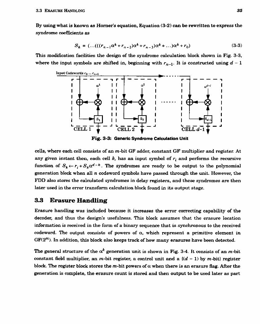
By using what is known as Horner's equation, Equation (3-2) can be rewritten to express the
syndrome coefficients as
Sk = (. . .(((rn - ,ak + r,, - ,)ak + r,, -,)ak + . . . )ak + rO) (3-3)
This modification facilities the design of the syndrome calculation block shown in Fig. 3-3,
where the input symbols are shifted in, beginning with r,-l. It is constructed using d - 1
Input Codewords ro ... r,,-~
1 1
L,- CELLI CËLLZ$-~ L - -
CELL d ~ i $ Fig. 3-3: Generic Syndrome Calculation Unit
cells, where each cell consists of an rn-bit GF adder, constant GF multiplier and register. At
any given instant then, each cell k, has an input symbol of ri and performs the recursive
fiinction of Sb c ri + S k a d - & . The syndromes are ready to be output to the polynomial
generation block when al1 n codeword symbols have passed through the unit. However, the
FDD also stores the calculated syndromes in delay registers, and these syndromes are then
later used in the error transform calculation block found in its output stage.
3.3 Erasure Handling
Erasure handling was included because it increases the error comecting capability of the
decoder, and thus the design's usehlness. This block assumes that the erasure location
information is received in the form of a binary sequence that is synchronous to the received
codeword. The output consists of powers of a, which represent a primitive element in
GF(2m). In addition, this block also keeps track of how many erasures have been detected.
The general structure of the cik generation unit is shown in Fig. 3-4. It consists of an rn-bit
constant field multiplier, an rn-bit register, a control unit and a ((d - 1) by rn-bit) register
block. The register block stores the rn-bit powers of ar when there is an eraswe flag. After the
generation is complete, the erasure count is stored and then output to be used later as part
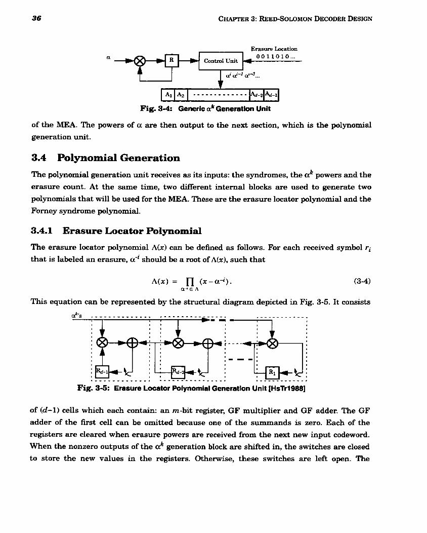
Erasure Lmation a! 0011010 ...
C o n h l Unit
Fig. 3-4: Generic a* Generation Unit
of the MEA. The powers of a are then output to the next section, which is the polynomial
generation unit.
3.4 Polynomial Generation
The polynomial generation unit receives as its inputs: the syndromes, the ak powers and the
erasure count. At the same tirne, two different interna1 blocks are used to generate two
polynomials that will be used for the MEA. These are the erasure locator polynomial and the
Forney syndrome polynomid.
3.4.1 Erasure Locator Polynomial
The erasure locator polynomial A(x) can be defined as follows. For each received symbol ri
that is labeled an erasure, üL should be a root of A(x), such that
This equation can be represented by the stmctural diagram depicted in Fig. 3-5. It consists
Fig. 3-5: Erasure Locator Polynomial Generation Unit [HsTr1988]
of (d-1) cells which each contain: an m-bit register, GF multiplier and GF adder. The GF
adder of the first ce11 can be omitted because one of the summands is zero. Each of the
registers are cleared when erasure powers are received from the next new input codeword.
When the nonzero outputs of the ak generation block are shif3ed in, the switches are closed
to store the new values in the registers. Otherwise, these switches are left open. The
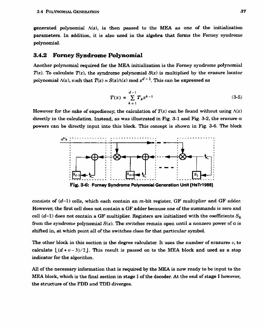
generated polynomial A(x), is then passed to the MEA as one of the initialization
parameters. In addition, it is also used in the algebra that forms the Forney syndrome
polynomial.
3.4.2 Forney Syndrome Polynomial
Another polynomial required for the MEA initialization is the Forney syndrome polynomial
nx). To calculate T(x), the syndrome polynomial S(x) is multiplied by the erasure locator
polynomial Nx), such that T(r) = S(x)A(x) mod 8 - ? This can be expressed as
However for the sake of expediency, the calculation of T(x) can be found without using A h )
directly in the calculation. Instead, as was illustrated in Fig. 3-1 and Fig. 3-2, the erasure a
powers can be directly input into this block. This concept is shown in Fig. 3-6. The block
Fig. 3-6: Forney Syndrome Polynomial Generstion Unit [HsTr1988]
consists of (d-1) cells, which each contain an m-bit register, GF multiplier and GF adder.
However, the first cell does not contain a GF adder because one of the suinmands is zero and
ce11 (d-1) does not contain a GF multiplier. Registers are initialized with the coefficients Sk from the syndrome polynomial S(x). The switches remain open until a nonzero power of ai. is
shifted in, a t which point al1 of the switches close for that particular symbol.
The other block in this section is the degree calculator. It uses the number of erasures v, to
calculate l ( d + v - 3)/2J. This result is passed on to the MEA block and used as a stop
indicator for the algorithm.
Al1 of the necessary information that is required by the JbEA is now ready to be input to the
MEA block, which is the final section in stage 1 of the decoder. At the end of stage 1 however,
the stmcture of the FDD and TDD diverges.
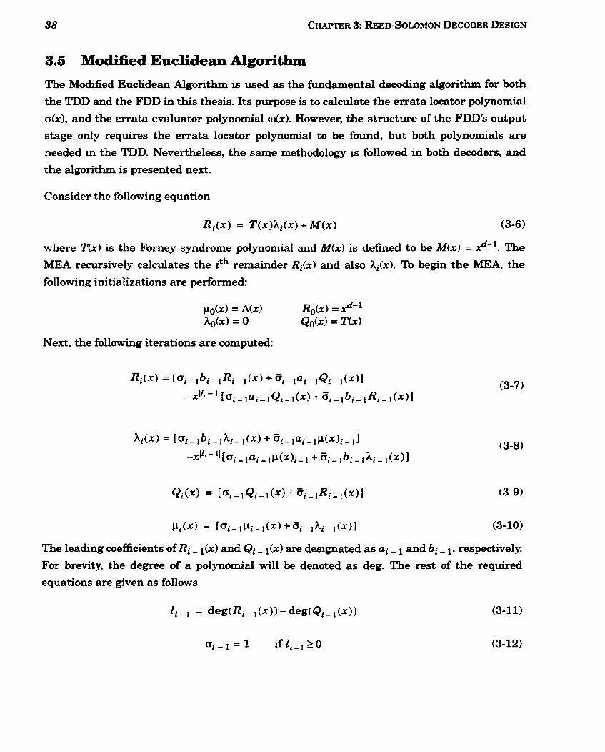
3.5 Modified Euclidean Algorithm
The Modified Euclidean Algorithm is used as the fundamental decoding algorithm for both
the TDD and the FDD in this thesis. Its purpose is to calculate the errata locator polynomial
a(x), and the errata evaluator polynomial dx) . However, the structure of the FDD's output
stage only requires the errata locator polynomial to be found, but both polynomials are
needed in the TDD. Nevertheless, the same methodology is followed in both decoders, and
the algorithm is presented next.
Consider the following equation
Ri(x) = T(x)hi(x) + M(x) (3-6)
where Th) is the Forney syndrome polynomial and M(x) is defined to be M(x) = xd-l. The
MEA recursively calculates the ith remainder Ri(x) and also Ai(x). To begin the MEA, the
following initializations are performed:
Next , the following iterations are computed:
pi(x) = [ ~ i - l ~ i - I ( ~ ) + Q i - I ~ i - l ( ~ ) I (3-10)
The leading coefficients of Ri _ l(x) and Qi - l(x) are designated as ai - 1 and bi - 1, respectively.
For brevity, the degree of a polynomial will be denoted as deg. The rest of the required
equations are given as follows
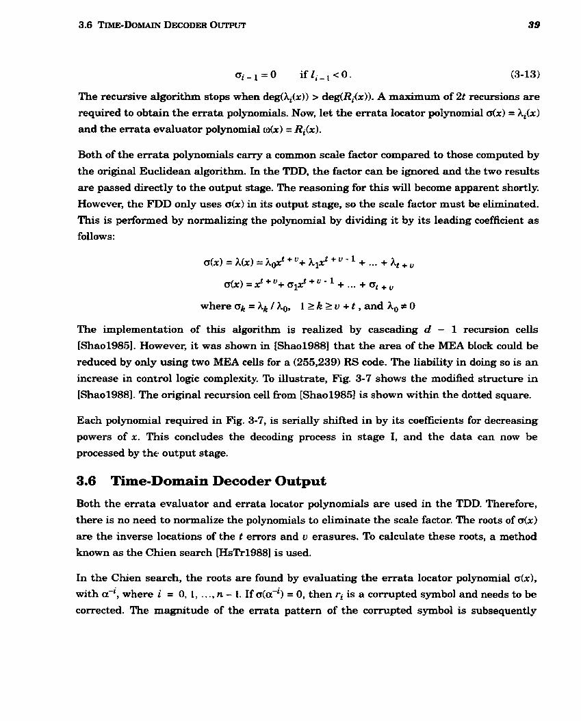
The recursive algorithm stops when deg(Ai(x)) > deg(Ri(x)). A maximum of 2t recursions are
required to obtain the errata polynomials. Now, let the errata locator polynomial dx) = Ai(x)
and the errata evaluator polynomial o ( x ) = Ri(x).
Both of the errata polynomials carry a common scale factor compared to those computed by
the original Euclidean algorithm. In the TDD, the factor can be ignored and the two results
are passed directly to the output stage. The reasoning for this will become apparent shortly.
However, the FDD only uses a(x) in its output stage, so the scale factor must be eliminated.
This is performed by normalizing the polynomial by dividing it by its leading coefficient a s
follows :
The implementation of this algorithm is realized by cascading d - 1 recursion cells
[Shao1985]. However, it was shown in Esha019881 that the area of the MEA block could be
reduced by only using two MEA cells for a (255,239) R S code. The liability in doing so is an
increase in control logic complexity. To illustrate, Fig. 3-7 shows the modified stmcture in
[Shao19881. The original recursion ce11 fkom [Shao19851 is shown within the dotted square.
Each polynomial required in Fig. 3-7, is serially shifted in by its coefficients for decreasing
powers of x. This concludes the decoding process in stage 1, and the data can now be
processed by the output stage.
3.6 Tirne-Domain Decoder Output
Both the errata evaluator and errata locator polynomials are used in the TDD. Therefore,
there is no need to normalize the polynomials to eliminate the scde factor. The roots of a(x)
are the inverse locations of the t errors and u erasures. To calculate these roots, a method
known as the Chien search [WsTr1988] is used.
In the Chien search, the roots are found by evaluating the errata locator polynomial cr(x),
with a-i, where i = 0, 1, . . ., n - 1. If a(a-i) = O, then ri is a corrupted symbol and needs to be
corrected. The magnitude of the errata pattern of the compted symbol is subsequently
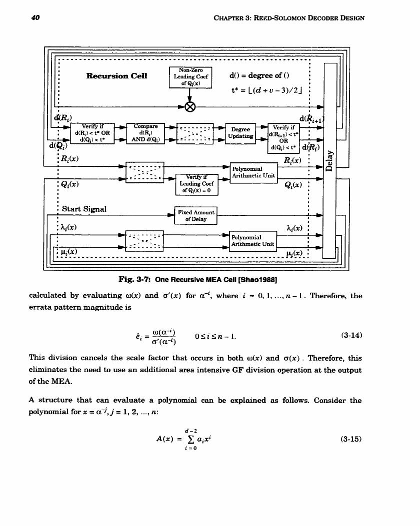
I 8
8 Non-km 8
rn Recursion Cell Leading coef dO = degree of O 8 of Qi(x) I
I
I t*= L(d+v-3 ) /2 j : 8 a I 8
I a
8 I
mi) Verifyii Corn-+.=. . - - - -; k d@i+ I
- - +- ; r : d(RJc t*OR d(R;) - . - - Updating d(Ri+i) t* - - - - - - - - - - - a d(Q$ c t* + AND d!Q$ -). OR r
- - d ( ~ ~ ) c t* ~ ( R ~ Y
8 C C - _ . . Arithmetic Unit Vedy if
: Qib) Leading Coef of QiW = O
a a I a I I
Start Signal a
Fixed Amount a a
I 8
8 of Delay a
hi(x) : a 8
8
* ~oiynomiai a Anthmetic Unit a
Fig. 3-7: One Recursive MEA Cell [Shao1988]
calculated by evaluating o(x) and d(x ) for à', where i = O, 1, . . ., n - 1 . Therefore,
errata pattern magnitude is
the
This division cancels the scale factor that occws in both o(x) and a(x) . Therefore, this
eliminates the need to use an additional area intensive GF division operation at the output
of the MEA.
A structure that can evaluate a polynomial can be explained as follows. Consider the
polynomial for x = ad, j = 1, 2, ..., n:
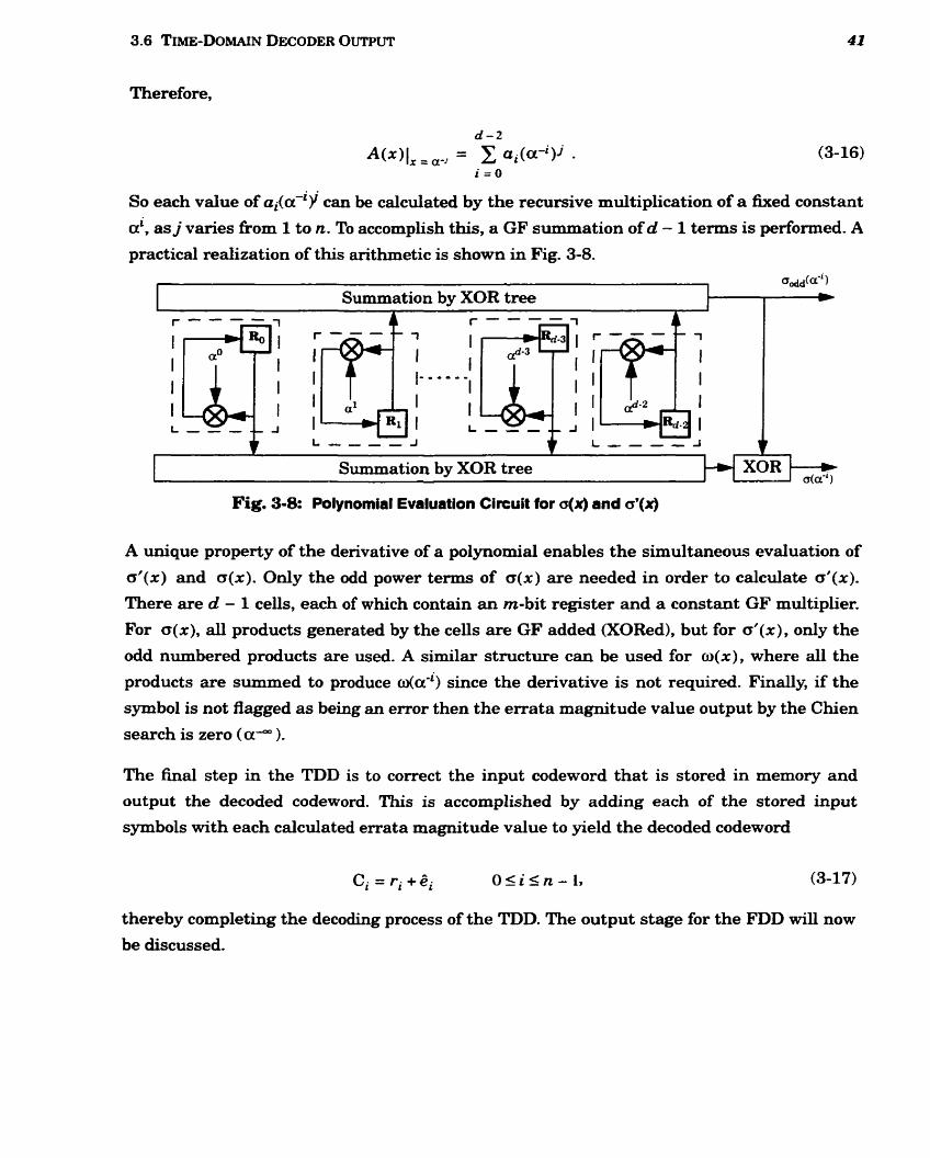
3.6 Tm-DOMAIN DECODER OUTPUT
Therefore,
d - 2
A ( x ) lx = - , = a,(a-l)j . (3- 16) i = O
So each value of ai(a-iy can be calculated by the recursive multiplication of a fixed constant
ai, as j varies fkom 1 to n. To accomplish this, a GF summation of d - 1 terms is performed. A
practical realization of this arithmetic is shown in Fig. 3-8.
1 Summation by XOR tree
- - -
Fig. 3-8: Polynomial Evaluation Circuit for o(x) and o'(x)
A unique property of the derivative of a polynomial enables the simultaneous evaluation of
a'(x) and o ( x ) . Only the odd power terms of a(x) are needed in order to calculate o' (x) .
There are d - 1 cells, each of which contain an rn-bit register and a constant GF multiplier.
For a(x), all products generated by the cells are GF added (XORed), but for o ' ( x ) , only the
odd numbered products are used. A similar structure can be used for o ( x ) , where all the
products are summed to produce da-') since the derivative is not required. Finally, if the
symbol is not flagged as being an error then the errata magnitude value output by the Chien
search is zero (cc- ).
The final step in the TDD is to correct the input codeword that is stored in memory and
output the decoded codeword. This is accomplished by adding each of the stored input
symbols with each calculated errata magnitude value to yield the decoded codeword
thereby completing the decoding process of the TDD. The output stage for the FDD will now
be discussed.

3.7 kequency-Domain Decoder Output
The FDD requires the errata locator polynomial a(x) , to be input from the MEA and not the
errata magnitude polynomial. However, o ( x ) must first be normalized in order to be in the
correct format for the remaining error transform block. The normalized version of o ( x )
dong with the stored syndromes corn stage 1 are used to calculate al1 of the errata
transforms.
3.7.1 Remaining Error Transform
The first d - 1 terms of the error transform Ek, are already known and they are the
syndromes £kom stage 1. To calculate the remaining transforms a recursive equation is used.
The remaining d 5 k 5 n elements of Ek are found by
For practical implementations, this equation can be realized with the configuratioc shown in
Fig. 3-9. The syndromes are serially input and form the first d - 1 elements of ER. There are
Syndromes .. -, S2, SI E m r Transform Sn,o,. Sn-l, ..., S2, S1
Fig. 3-9: Remaining Error Transform Block
d - 1 cells each containing two m-bit registers, an rn-bit GF multiplier and an m-bit GF
adder. However, in ce11 d - 1, the adder is omitted because one of the siimmands is zero. The
values shifted out of register RI are the error transforms after the d - 1 syndromes are
shified through. Nonzero coefficients from the normalized errata transform polynomial
a @ ) , initialize the second register in each cell. Once al1 n error transforms have been
sbifted out, the next step in the FDD is to calculate the inverse error transforms that will be
used to correct the input codeword.
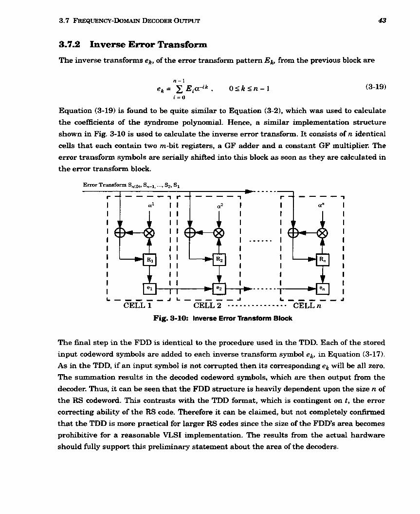
3.7.2 Inverse E m r Transforni
The inverse transforms ek, of the error transform pattern Ek, fsom the previous block are
Equation (3-19) is found to be quite similar to Equation (3-Z), which was used to calculate
the coefficients of the syndrome polynornid. Hence, a similar implementation structure
shown in Fig. 3-10 is used to calculate the inverse error transform. It consists of n identical
ceUs that each contain two m-bit registers, a GF adder and a constant GF multiplier. The
error transform symbols are serially shifted into this block as soon as they are calculated in
the error transform block.
Fig. 3-10: Inverse Error Transform Block
The final step in the FDD is identical to the procedure used in the TDD. Each of the stored
input codeword symbots are added to each inverse transform symbol e b in Equation (3-17).
As in the TDD, if an input symbol is not corrupted then its corresponding ek will be all zero.
The siimmation results in the decoded codeword symbols, which are then output fkom the
decoder. Thus, it can be seen that the FDD structure is heavily dependent upon the size n of
the RS codeword. This contrasts with the TDD format, which is contingent on t, the error
correcting abiiity of the RS code. Therefore it can be claimed, but not completely confiinied
that the TDD is more practical for larger RS codes since the size of the FDD's area becomes
prohibitive for a reasonable VLSI implementation. The results from the actual hardware
should fully support this preliminary statement about the area of the decoders.
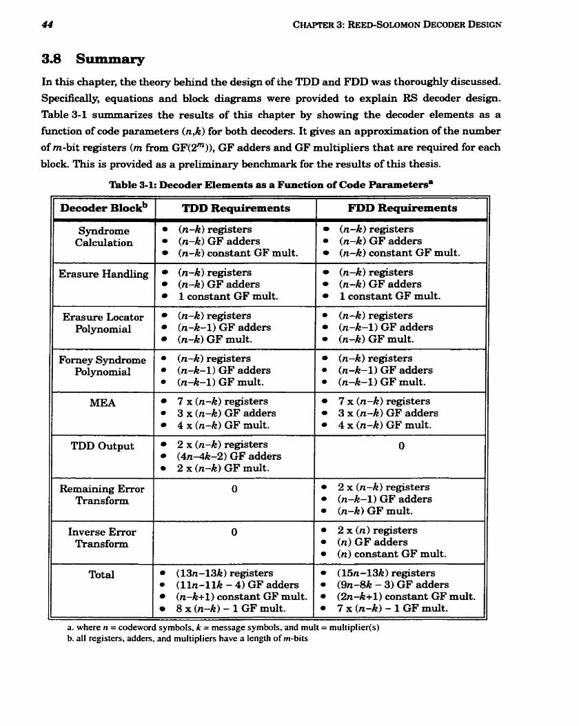
3.8 Summary
In this chapter, the theory behind the design of the TDD and FDD was thoroughly discussed.
Specifically, equations and block diagrams were provided to explain RS decoder design.
Table 3-1 slimmarizes the results of this chapter by showing the decoder elements as a
function of code parameters (n,k) for both decoders. It gives an approximation of the number
of rn-bit registers (rn from GF(2m)), GF adders and GF multipliers that are required for each
block. This is provided as a preliminary benchmark for the results of this thesis.
a b l e 3-1: Decoder Elements as a Function of Code Parametersa
Syndrome Calculation
Erasure Handling
Erasure Locator Polynomial
--
Forney Syndrome Polynomial
TDD Output
-
Remaining Error Transform
Inverse Error Transform
Tot al
TDD Requirements 1 FDD Requirements
(n-k) registers (n-k) GF adders 1 constant GF mult.
(n-k) registers (n-k) GF adders (n-k) constant GF mult.
(n-k) registers (n-k) GF adders 1 constant GF mult.
(n-k) registers (n-k) GF adders (n-k) constant GF mult.
(n-k) registers (n-k-1) GF adders (n-k) GF mult.
(n-k) registers (n-k-1) GF adders (n-k) GF mult.
-- -
(n-k) registers (n-k-1) GF adders (n-k-1) GF mult.
- - - - - - - - -
(n-k) registers (n-k-1) GF adders (n-k-1) GF mult.
7 x (n-k) registers 3 x (n-k) GF adders 4x(n-k)GFmult.
7 x (n-k) registers 3 x (n-k) GF adders 4 x (n-k) GF mult.
2 x (n-k) registers (4n-4k-2) GF adders 2 x(n-k)GFmult.
- - - - - - - -
2 x ( n - k ) registers (n-k-1) GF adders (n-k) GF mult.
2 x (n) registers (n) GF adders (n) constant GF mult.
a. where 12 = codeword symbols, k = message symbols, and mult = multiplier(s) b. a11 registers, adders, and multipliers have a length of ni-bits
(13n-13k) registers ( l ln - l lk - 4) GF adders (n-k+1) constant GF mult. 8 x (n-k) - 1 GF mult.
(15n-13k) registers (9n-8k - 3) GF adders (2n-k+l) constant GF mult. 7x(n-k)-1GFmult .
3.8 SUMMARY
In short:
A basic implementation overview of both the TDD and FDD was shown, which divided the decoding process into distinct stages and blocks.
The mathematical theory governing the designs of an RS TDD and FDD were presented,
including a general explanation of how to practically realize each section.
It was shown that both decoders are essentially identical up to the Modified Euclidean Algorithm. The main difference is the structure of the output stages of each decoder.
The following chapter presents the VLSI design and peliormance results of each of the RS decoder implementations.

Chapter El Hardware Implementation
One of the fiindamental objectives of this thesis was to implement both the FDD and TDD in
VLSI hardware in order to ascertain a defmitive statement about the two RS decoder
implementations. Chapter 3 elaborated on the algebra and theory that are used to constmct
RS decoders. Both the TDD and the FDD were discussed in terms of the mathematics and
structure involved in each approach.
In this chapter the hardware design, VLSI methodology, and final test results for each
decoder will be presented. A silicon implementation of the TDD was produced and the FDD was designed up to the point of, but not including actual fabrication. Chapter 4 is divided
into three sections. First, the TDD VLSI approach is explained, which is then followed by the
FDD hardware presentation. Finally, the last section offers a comparative analysis of the
two decoding approaches.
4.1 Reed-Solomon Tirne-Domain Decoder
The design of the RS TDD followed the structure outlined in the previous chapter. However,
this thesis attempted to achieve the most optimal RS decoder in terms of area and power
consumption while maintaining a sufficient speed to meet the target application's timing
requirements. Therefore, some modifications were made to improve the efficiency of the
design.

4.11 VLSI Architecture
The structure of the RS decoder chip was chosen to be comparable to existing products
available today such as those in [Core2000], ~ 2 0 0 0 1 and [4i2i2000]. The RS design in
[Core2000] was only preliminary and no real specifications were provided as to its
performance. However, it required two extemal synchronous double-port RAM blocks with a
dock input, an active-low write-enable input, an address input and an active-low chip-
enable input. Another HDL RS core implementation was found in [4i2i2000J. This design
included the encoder, optional erasure decoding, parameterizable (n,k) RS code size, and
other optional features. An estimate of the number of gates for a maximum t = 8 RS encoder/
decoder was given as 47 000 gates, of which 35 000 were used for the decoder. For a (255,239)
RS code, the decoding speed was stated as being 4500 clocks per codeword. No specific rates
were provided though. Finally, [Xili2000] markets an FPGA realization of an RS decoder. It
can implement a variety of codes including symbol sizes ranging from three to twelve bits. In
addition, it can support erasures and different primitive polynomials. For a (204,188) RS code for DVB, the following specifications were provided for the XC4000/Spartan FPGA: no
erasure support, 8-bit symbols, 702 configurable logic blocks (CLBs) with 82 unused CLBs,
and a maximum dock frequency of 47MHz.
The designs in this thesis target a (255,239) RS code that incorporates erasure handling.
These decoders have an error correcting capability of t = m = 8 errors. Overall the decoder
can correct e errors and v erasures provided that v + 2e Id - 1, where d - 1 = 16. Although
the structure of the TDD resembles that presented in the previous chapter, it is
architect urally different .
As a preliminary estimate, the results from Table 3-1 in Chapter 3 are used to compare the
hardware requirements of a TDD and an FDD before any optimizations are performed.
Based on the target (255,239) RS code, the following components are required:
Table 4-1: Non-Optimized Hardware Requirements for (255,239) RS Decoders
Hardware
Registers @-bit)
GF Adders (8-bit)
Constant GF Multiplier (8-bit)
GF Multiplier (8-bit)
TDD
208
172
17
127
FDD
718
386
272
111
These hardware requirements are for a general case RS decoder and do not take into
consideration a r c h i t e c t d optimizations, control logic or required memory blocks. In
particular, the TDD has added area and complexity to that shown in the table with its
memory requirement. At this early stage however, it can be seen that the TDD appears to be
superior to the FDD in terms of the siücon area requirement. Yet a t this point, it is difEcult
to quantitatively estimate the relative area benefits of one irnplementation over the other
one. Modifications were made in order to achieve an optimal area for each design.
The design was partitioned into the following four pipelined stages:
(il Syndrome calculation block, ak generation block and input symbol memory block.
(ii) Forney syndrome polynomial calculation block, degree calculation block, erasure locator polynomial generation block, and MEA block.
(iii) Chien search unit.
(iv) Decoding status determination (Success/Failure?) and GF addition of the decoded symbols with the delayed input symbols.
This design used two clocks: clock and symbol-clock. The dock was chosen to be four times
the speed of syrnbol-clock and both clocks were completely in phase. Moreover, syrnbolclock
was responsible for driving Aip-flops that had the codeword symbols as inputs and was
targeted to operate a t 20MHz. The clock was used everywhere else in order to be able to
achieve the speeds of the target applications. For instance, symbol-dock clocked the received
symbols into the decoder and the decoded symbols out of the decoder. However, dock was
used in areas such as controller blocks. The length of time required for each pipeline stage
was 255 synbol-dock cycles. This was the amount of time required to shiR in one RS
codeword.
The reasons for choosing the preceding clock scheme were as follows. First, an attempt was
made to have the decoder be consistent with current implementations, such as those found
in [Core2000]. This would increase the applicability of the results fkom this thesis. Second,
the optimized area design of the modined Chien search block from [Kwon1997] was used
instead of the traditional approach in [Shao1988]. A significant savings in area was realized
by using the modified design, but the trade-off was that a faster clock was needed to meet
the timing requirements. This approach was taken because area was an important design
parameter that this thesis focused on optimizing. Finally, this clocking scheme was suitable
for the available memory core modules. The division of the pipeline stages and
implementation of the memory cores were facilitated by using these clock rates. This will be
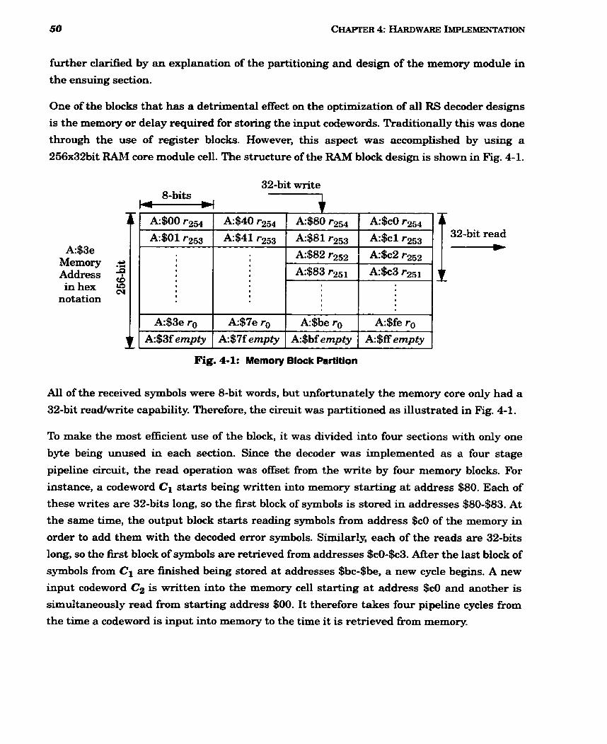
W h e r clarified by an explanation of the partitioning and design of the memory module in
the ensuing section.
One of the blocks that has a detrimental effect on the optimization of al1 RS decoder designs
is the memory or delay required for storing the input codewords. Traditionally this was done
through the use of register blocks. However, this aspect was accomplished by using a
256x32bit RAn4 core module cell. The stmcture of the RAM block design is shown in Fig. 4-1.
A:$3e Memory a q Address in hex
notation
Fig. 4-1: Memory Block Partition
32-bit write 8-bits -
AU of the received symbols were 8-bit words, but unfortunately the memory core only had a
32-bit read/wnte capability. Therefore, the circuit was partitioned as illustrated in Fig. 4-1.
A:$OO r254
A:$01 r253
1
I
8
8
I
8
8
I
A:$3e ro A:$3f empty
To make the most efficient use of the block, it was divided into four sections with only one
byte being unused in each section. Since the decoder was implemented as a four stage
pipeline circuit, the read operation was offset from the write by four memory blocks. For
instance, a codeword Cl starts being written into memory starting a t address $80. Each of
these writes are 32-bits long, so the first block of symbols is stored in addresses $80-$83. At
the same time, the output block starts reading symbols from address $CO of the memory in
order to add them with the decoded error symbols. Similady, each of the reads are 32-bits
long, so the first block of symbols are retrieved from addresses $CO-$c3. m e r the last block of
symbols from Ci are finished being stored at addresses $bc-$be, a new cycle begins. A new
input codeword C2 is written into the memory cell starting a t address $CO and another is
simultaneously read from starting address $00. It therefore takes four pipeline cycles from
the tirne a codeword is input into memory to the time it is retrieved fkom memory.
A:$40 î254
A:$41 r253
8
I
I
I
8
8
A:$7e ro A:$7f empty
A:$80 r2s4
A : $ 8 1 r ~ ~ ~
A:$82 r252
A:$83 ~ 5 1
I
I
8
A:$be ro A:$bf empty
A:$cO r254
A:$cl r253 32-bit read - A:$c2 rzs2 A:$c3 rzsi
l
I
A:$fe ro A:$ ff empty
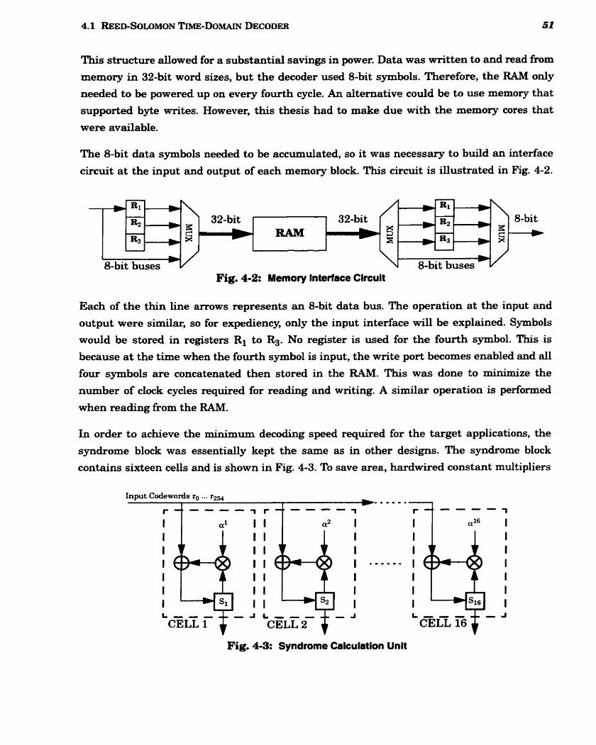
This structure allowed for a substantial savings in power. Data was written to and read f?om
memory in 32-bit word sizes, but the decoder used 8-bit symbols. Therefore, the RAM only
needed to be powered up on every fourth cycle. An alternative could be to use memory that
supported byte writes. However, this thesis had to make due with the memory cores that
were available.
The 8-bit data symbols needed to be accumulated, so it was necessary to build an interface
circuit at the input and output of each memory block. This circuit is illustrated in Fig. 4-2.
Each of the thin line arrows represents an 8-bit data bus. The operation at the input and
* Rl rn R1
output were similar, so for expediency, only the input interface will be explained. Symbols
would be stored in registers Ri to R3. No register is used for the fourth symbol. This is
- R2 32-bit
because at the t h e when the fourth symbol is input, the write port becomes enabled and al1
-
four symbols are concatenated then stored in the RAM. This was done to minimize the
number of clock cycles required for reading and writing. A similar operation is performed
32-bit
when reading from the RAM.
- R3 . -
In order to achieve the minimum decoding speed required for the target applications, the
syndrome block was essentially kept the same as in other designs. The syndrome block
8-bit buses Fige 4-2: Memory Interface Circuit
RAM
contains sixteen cells and is shown in Fig. 4-3. To Save area, hardwired constant multipliers
1 ) S - 2 1 rn R3 :
Fige 4-3: Syndrome Calculation Unit
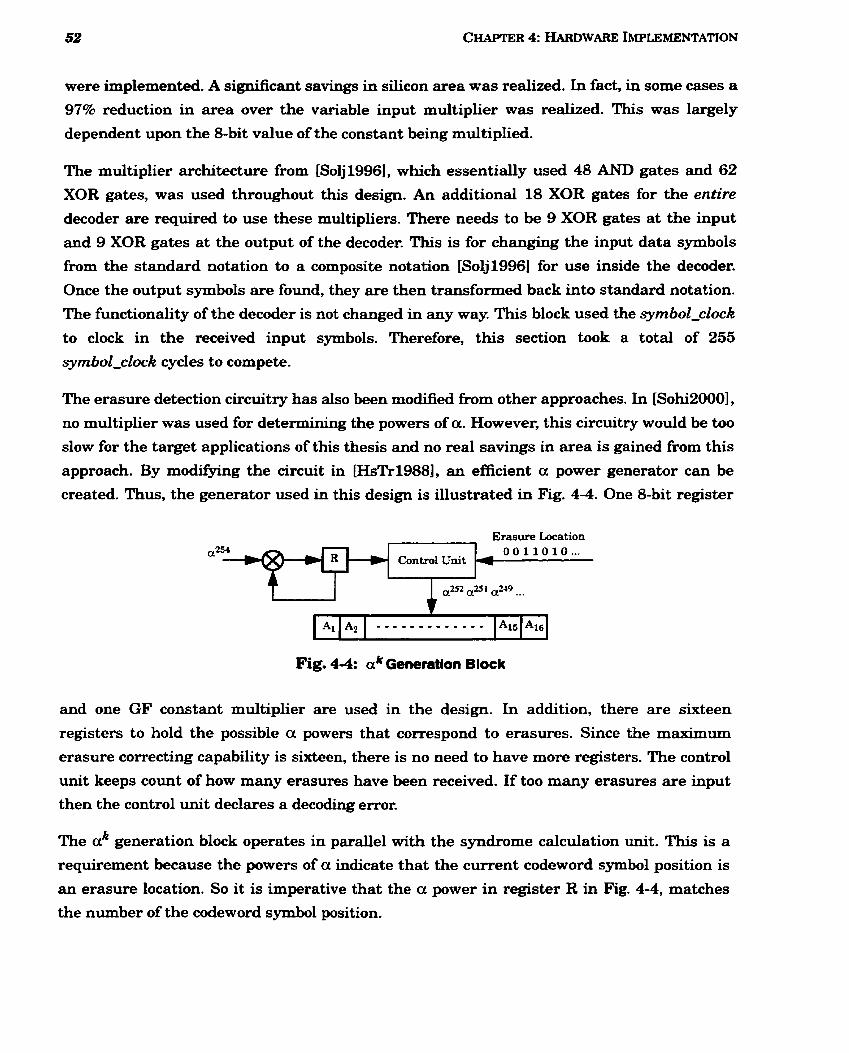
were implemented. A significant savings in silicon area was realized. In fact, in some cases a
97% reduction in area over the variable input multiplier was realized. This was largely
dependent upon the &bit value of the constant king multiplied.
The multiplier architecture corn [Solj1996], which essentially used 48 AND gates and 62
XOR gates, was used throughout this design. An additional 18 XOR gates for the entire
decoder are required to use these multipliers. There needs to be 9 XOR gates at the input
and 9 XOR gates at the output of the decoder. This is for changing the input data symbols
from the standard notation to a composite notation [Solj1996] for use inside the decoder.
Once the output symbols are found, they are then transformed back into standard notation.
The hctionality of the decoder is not changed in any way This block used the syrnbol-dock
to clock in the received input symbols. Therefore, this section took a total of 255
syrnbol-dock cycles to compete.
The erasure detection circuitry has also been modified fkom other approaches. In [Sohi2000],
no multiplier was used for determining the powers of a. However, this circuitry would be too
slow for the target applications of this thesis and no real savings in area is gained Fom this
approach. By mo+g the circuit in [HsTr1988], an efficient a power generator can be
created. Thus, the generator used in this design is illustrated in Fig. 4-4. One &bit register
Erasure Location
Fig. 4-4: ak Generation Block
Control Unit
and one GF constant multiplier are used in the design. In addition, there are sixteen
registers to hold the possible a powers that correspond to erasures. Since the maximum
erasure correcting capability is sixteen, there is no need to have more registers. The control
unit keeps count of how many erasures have been received. If too many erasures are input
then the control unit declares a decoding error.
0011010 ... 4
The ak generation block operates in parallel with the syndrome calcdation unit. This is a
requirement because the powers of a indicate that the current codeword symbol position is
an erasure location. So it is imperative that the a power in register R in Fig. 4-4, matches
the number of the codeword symbol position.
,252 ,ZS 1 a249 .-.
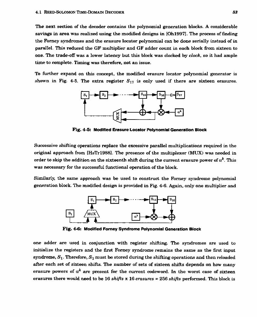
The next section of the decoder contains the polynomial generation blocks. A considerable
savings in area was realized using the modified designs in [0h1997]. The process of finding
the Forney syndromes and the erasure locator polynomial can be done serially instead of in
parallel. This reduced the GF multiplier and GF adder count in each block fkom sixteen to
one. The trade-off was a lower latency but this block was clocked by dock , so it had ample
time to complete. Timing was therefore, not an issue.
To W h e r expand on this concept, the m d e d erasure locator polynomial generator is
shown in Fig. 4-5. The extra register SIS is only used if there are sixteen erasures.
Fig. 4-5: Modif ied Erasure Locator Polynomial Generation Block
Successive sbifting operations replace the excessive parallel multiplications required in the
original approach from [HsTr1988]. The presence of the multiplexor (MUXI was needed in
order to skip the addition on the sixteenth shift during the m e n t erasure power of ak. This
was necessary for the successful functional operation of the block.
Similaris the same approach was be used to construct the Forney syndrome polynomial
generation block. The modified design is provided in Fig. 4-6. Again, only one multiplier and
Fig. 4 4 Modified Forney Syndrome Polynomial Generation Block
one adder are used in conjunction with register shifting. The syndromes are used to
initialize the registers and the e s t Forney syndrome remains the same as the fmst input
syndrome, SI. Therefore, SI must be stored during the shifting operations and then reloaded
aRer each set of sixteen shifts. The number of sets of sixteen shiRs depends on how many
erasure powers of cik are present for the current codeword. In the worst case of sixteen
erasures there would need to be 16 shifts x 16 erasures = 256 shifts performed. This block is

clocked with dock and the number of cycles that it takes to complete Vary with the number
of erasures present in the input codeword.
The next architectural improvement was with the MEA. [Shao1988] suggested that for a
(255,239) RS decoder, two MEA cells can be used repetitively instead of using sixteen
cascaded cells. The savings in area was offset by the increased complexity of the control
module for this block. However, it was found that only one MEA cell was needed to meet the
timing requirements of the target applications if clwk was used. The outputs of the MEA cell
are delayed and then fed back as inputs. Therefore by using a single MEA cell, the decoder
area is dramatically reduced and the overd complexity is simpliiied as well. The completion
time is highly irregular and varies according to the codeword and the number of errors and
erasures that are present. However, there was always sdc i en t time for the decoding to
complete because of the timing requirements of the preceding and succeeding pipeline
stages.
As previously mentioned, the Chien search unit was also modified from the traditional
approach in [Shao1988]. By using the suggested architecture in [0h1997], the area of this
block was reduced significantly. The new structure is illustrated in Fig. 4-7. Hardware blocks
I uodd(a~i)
.)
"O
. . -. . . . .
V o(a-'
Summation by XOR tree XOR h Fig. 4-7: Modified Chien Search Block
are shared to compute aWi), oaodd(a-') and ~ ( a - ~ ) . The results can be summarized as follows:
(il Reduction from 4 XOR tree summation blocks to 2.
(ii) Reduction from 33 GF multipliers to 17.
(iii) Completion time was doubled.
Timing was not an issue since dock was used, The main objective here was to reduce the
area for the RS decoder. During even dock cycles, a(&) and ~ ~ ~ ( a - ~ ) are computed, while

during odd cycles, is computed. In addition, a memory cell was used to store the error
symbol results fkom the Chien search block. The memory module architecture and design
were similar to the ones used for storing the input codewords (Fig. 4-1 and Fig. 4-2). The
non-zero error pattern symbols that are generated from the Chien search are counted, and
then used to determine if a decoder failure has occurred.
The Chien search block involved calculating the errata pattern magnitudes, which were
stated previously in Equation 3-14 as being
o(~- ' ) O s i l n - 1. 4 = a'o
This step involved a GF division. A hite-field division can be partitioned into two separate
operations: an inversion and a multiplication. Instead of using an area intensive 255xSbit
look-up table for inverses, a much more optimal approach from [Solj1996] was used. The
inverter used 58 AND and 71 XOR gates. Furthemore, this divider implementation also
reduced the complexity involved with a GF division. Using a look-up table would require
additional complicated control circuitry to retrieve the correct inverse symbol. Designs can
be facilitated by using the simple, but yet highly efficient architecture in [Solj 19961.
Power consumption in the RS decoder was attempted to be reduced as well. This was
accomplished by using the error and erasure information generated by the decoder. For
instance, if the sixteen syndromes are all calculated to be zero then there are no errors, and
the entire decoding process c m be skipped. Thus, registers invo1ved in decoding are not
enabled, which reduces the power consumption.
In addition, memory cores were used where possible to reduce the n u b e r of register
shifting operations. Moreover, the memory blocks were disabled when not reading or writing
to them. In fact, the memory blocks were only powered on one out of every four clock cycles.
The data bus was 32-bits wide, but the data of the decoder was 8-bits wide. This means that
data needs to be accumulated for a write and partitioned for a read.
The following is a description of a write operation that serves to illustrate the power
conservation operation of the memory. To begin, the term "clock" in the following explanation
wiU refer to either the ctock or syrnbol-dock. The write operation is the same regardless of
which clock is comected to the memory's clock ports. Three bytes of data are stored in three
temporary &bit registers over a duration of three "clock" cycles. Then upon the fourth "clock"
cycle, the last byte of data is concatenated to the first three bytes of data. The memory is
enabled and the 32-bits of data are written in at this time. A similar procedure was used for
reading data h m the memory as well. In that case, data is shiRed out in 32-bit lengths and
then partitioned and stored in temporary registers.
The memory approach eliminates the need of having 255 &bit registers, which are switching
at the same tirne on every "clock" cycle. In addition, a m h e r reduction in power
consurnption was achieved by using the 32-bit read/write size of the memory data bus. This
allowed the RAM to be powered down for three out of every four "clock" cycles. The address
decoding and word lines did not have to be powered up continually. This is important
because these two blocks could substantially increase the power requirement if they were
required to be powered up continuously. Thus, a considerable savings in power was realized
by powering down the memories when they were not in use.
An improved RS TDD design in terms of area optimization and power reduction was
achieved by implementing the preceding architectural modifications. The next section
presents the VLSI results fkom the fabrication of this decoder design.
4.1.2 Implementation Results
The fùnctionality of the RS TDD was verified through the use of MATLAB code, which is
provided in Appendix B. Once the algorithm operated correctly, the design was implemented
using Verilog. The testing procedure was based on a bottom-up approach. Each lower level
module was designed, coded and then tested with separate testbenches. Then, this
methodology was repeated when these blocks were combined to form a new level of
hierarchy. To increase the likelihood of a successfd fabrication, testing occurred at several
stages of the design. Once the HDL coding of the entire decoder was complete, it was verified
to operate correctly through the use of a global testbench. Then aiter synthesis in Synopsys,
the gate-level netlist was tested with the same testbench and verified. The last test
confirmed that the post-layout, gate-level netlist fùnctioned correctly. This was the TDD design that was fabricated. For static timing analysis, Pearl was used to verify that there
were no setup or hold violations for the decoder.
The RS TDD was implemented in a six-metal layer 0.18pm CMOS process technology. A
standard-cell automated place-and-route was used to generate the layout in order to reduce
design tirne. The pins on the chip are listed and described in Table 4-2. Both the TDD and
the FDD used the same pin configuration. Similarly, for both decoders, there were several
pins which were not used. The reasoning for this is explained in Section 4.1.3.
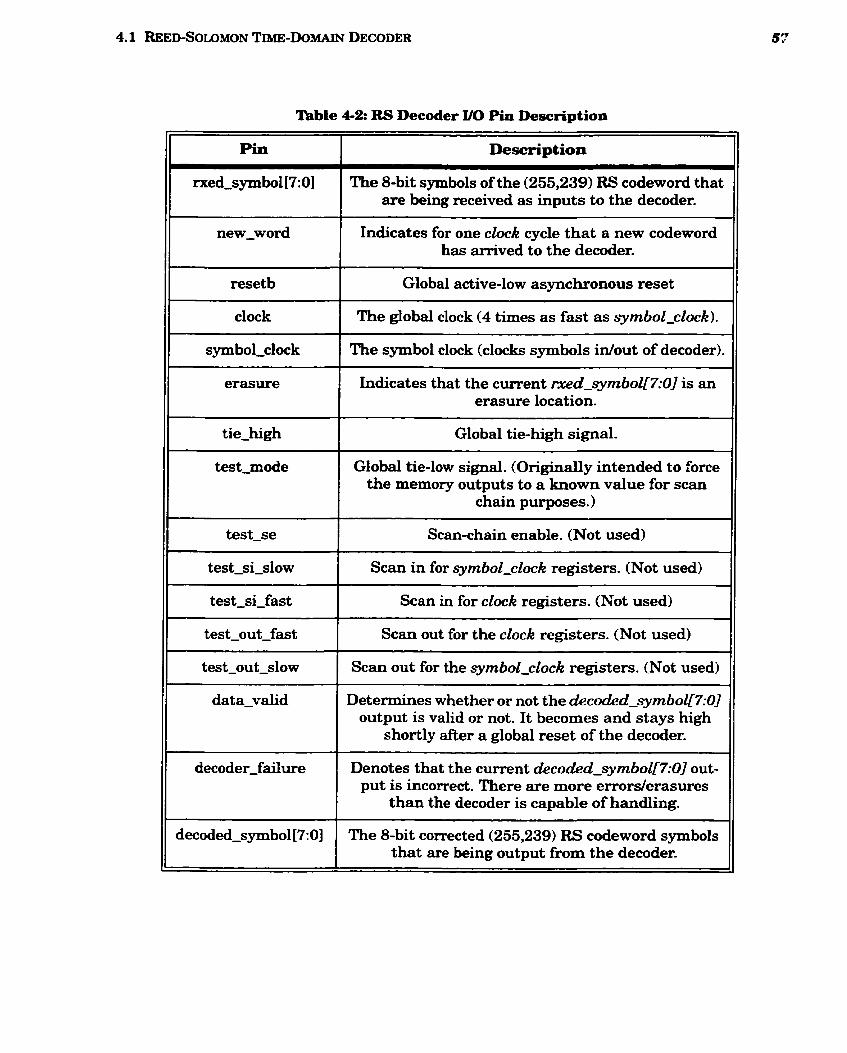
Table 42: RS Decoder UO Pin Description
II Pin
II resetb
II clock
1) symbol-clock
II erasure
tes t-mode
l l test-se
II test-si-slow
II test-si-fast
II test-out-fast
dat a-valid
decoderfailure
Description
The $-bit symbols of the (255,239) RS codeword that are king received as inputs to the decoder.
Indicates for one clock cycle that a new codeword has arrived to the decoder.
Global active-low asynchronous reset -- - -
The global clock (4 times as fast as symbol-dock).
The symbol clock (clocks symbols idou t of decoder).
Indicates that the current rxed-symbol[7:0] is an erasure location.
Global tie-high signal. - -
Global tie-low signal. (Originally intended to force the memory outputs to a known value for scan
c h a h purposes.) -
Scan-chain enable. (Not used)
Scan in for syrnbol-clock registers. (Not usedl
Scan in for clock registers. (Not used)
Scan out for the dock registers. (Not used)
Scan out for the symbol-clock registers. (Not used)
Determines whether or not the decocïedcEsymbolf7:0] output is valid or not. It becornes and stays high
shortly after a global reset of the decoder.
Denotes that the cu ren t decoded-symbol[7:0. out- put is incorrect. There are more errorderasures
than the decoder is capable of handling.
The 8-bit corrected (255,239) RS codeword symbols that are being output from the decoder.
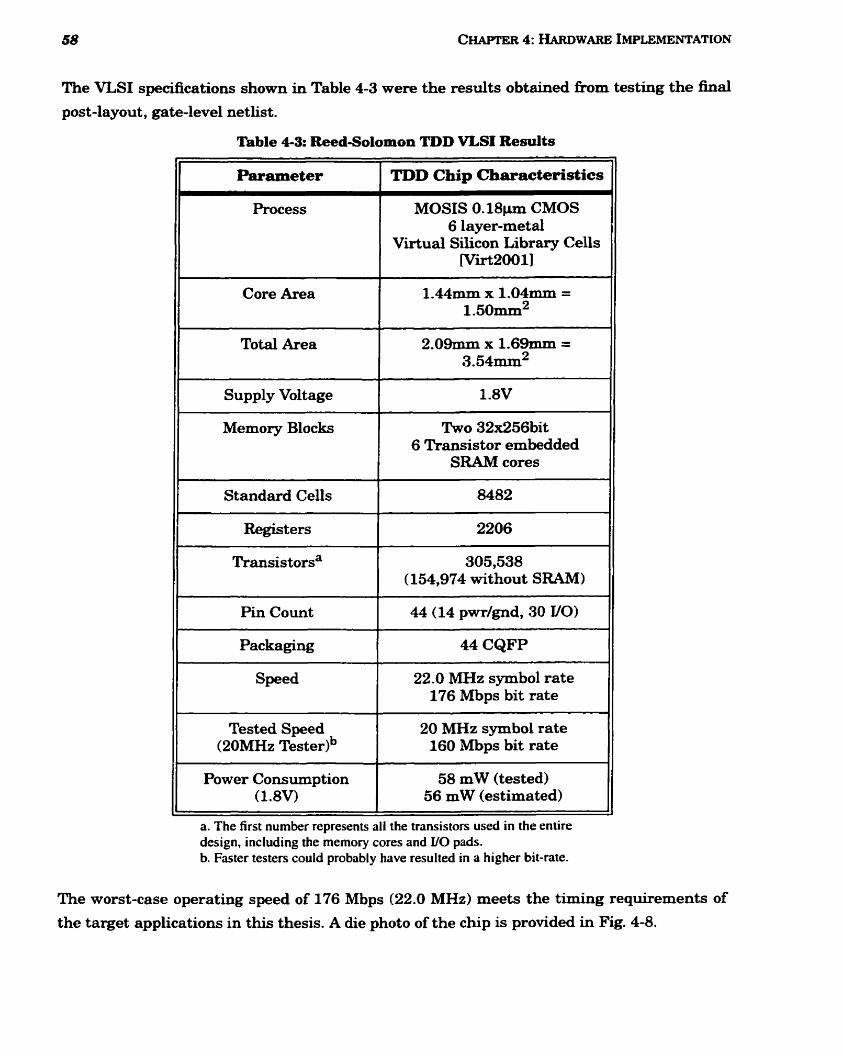
58 CHAPTER 4: HARDWARE IMPLEMENTATION
The VLSI speQfications shown in Table 4-3 were the results obtained 60m testing the final post-layout, gate-level netlist.
Table 4-3: Reed-Solomon TDD VLSI R e d t s
1 Parameter 1 TDD Chip Characteristics
MOSIS O.18pm CMOS 6 layer-metd
Virtual Silicon Library Cells [VirtZOOl]
Core Area
Total Area
supply Voltage 1 Memory Blocks Two 32x256bit
6 Transistor embedded SRAM cores
-- 1) Standard Cells 7 8482
I / Regist ers I 2206
II Transis torsa 305,538 (154,974 without SRAM)
Pin Count
Packaging 44 CQFP
Speed
Tested Speed (20MHz ester)^
The worst-case operating speed of 176 Mbps (22.0 MHz) meets the timing requirements of
the target applications in this thesis. A die photo of the chip is provided in Fig. 4-8.
22.0 MHz symbol rate 176 Mbps bit rate
20 MHz symbol rate 160 Mbps bit rate
Power Consumption (1.8V)
58 mW (tested) 56 mW (estimatedl
a. The first number represents all the transistors used in the entire design, including the memory cores and il0 pads. b. Faster testers could probably have resulted in a higher bit-rate.
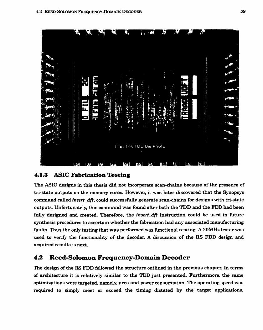
4.1.3 ASIC Fabrication Testing
The ASIC designs in this thesis did not incorporate scan-chains because of the presence
tri-state outputs on the memory cores. However, it was later discovered that the Synopsys
command called insert-dft, could successfully generate scan-chahs for designs with tri-state
outputs. Wortunately, this command was found after both the TDD and the FDD had been
fully designed and created. Therefore, the insert-dft instruction could be used in future
synthesis procedures to ascertain whether the fabrication had any associated manufaduring
faults. Thus the only testing that was performed was fiinctional testing. A 20MHz tester was
used to verify the fundionality of the decoder. A discussion of the RS FDD design and
acquired results is next.
4.2 Reed-Solomon Frequency-Domain Decoder
The design of the FU FDD followed the structure outlined in the previous chapter. In terms
of architecture it is relatively sirnilar to the TDD just presented. Furthemore, the same
optimizations were targeted, namely, area and power consumption. The operating speed was
required to simply meet or exceed the timing dictated by the target applications.
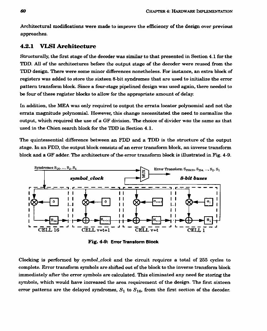
Architectural modifications were made to improve the efficiency of the design over previous
approaches.
4.2.1 VLSI Architecture
Structurally, the first stage of the decoder was similar to that presented in Section 4.1 for the
TDD. AU of the architectures before the output stage of the decoder were reused from the
TDD design. There were some minor differences nonetheless. For instance, an extra block of
registers was added to store the sixteen 8-bit syndromes that are used to initialize the error
pattern transfonn block. Since a four-stage pipelined design was used again, there needed to
be four of these register blocks to allow for the appropriate amount of delay.
In addition, the MEA was only required to output the errata locator polynomial and not the
errata magnitude polynomial. However, this change necessitated the need to normalize the
output, which required the use of a GF division. The choice of divider was the same as that
used in the Chien search block for the TDD in Section 4.1.
The quintessential difference between an FDD and a TDD is the structure of the output
stage. In an FDD, the output block consists of an error transform block, an inverse transfonn
block and a GF adder. The architecture of the error transform block is illustrated in Fig. 4-9.
Fig. 4-9: Error Transform Block
Clocking is performed by symbol-dock and the circuit requires a total of 255 cycles to
complete. Error transform symbols are shifted out of the block to the inverse transform block
immediately after the error symbols are caiculated. This eliminated any need for storing the
symbols, which would have increased the area requirement of the design. The f is t sixteen
error patterns are the delayed syndromes, S1 to S16, eom the first section of the decoder.
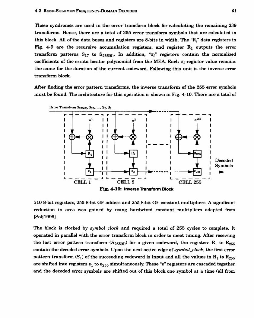
These syndromes are used in the error transform block for calculating the remRining 239
transforms. Hence, there are a total of 255 error transfonn symbols that are calculatecl in
this block. All of the data buses and registers are 8-bits in width. The qn data registers in
Fig. 4-9 are the recursive accumulation registers, and register RI outputs the error
transform patterns SI7 to S255(0p In addition, "oin registers contain the normalized
coefficients of the errata locator polynomial from the MEA. Each ai register value remains
the same for the duration of the current codeword. Following this unit is the inverse error
transform block.
m e r finding the error pattern transforms, the inverse transform of the 255 error symbols
must be found. The architecture for this operation is shown in Fig. 4-10. There are a total of
I I I I I I I I I I I I I I I Decoded
I Symbols I
I
Fig. 4-10: Inverse Transform Block
510 &bit registers, 255 &bit GF adders and 255 &bit GF constant multipliers. A significant
reduction in area was gained by using hardwired constant multipliers adapted from
[solj 19961.
The block is clocked by syrnbol-clock and required a total of 255 cycles to complete. It
operated in parallel with the error transform block in order to meet timing. M e r receiving
the last error pattern transform (S255to)) for a given codeword, the registers Ri to R255 contain the decoded error symbols. Upon the next active edge of syrnbol-dock, the first error
pattern transform (Si) of the succeeding codeword is input and al1 the values in RI to R255 are &Red into registers el to e255 simultaneously. These "en registers are cascaded together
and the decoded error symbols are shiRed out of this block one symbol at a time (al1 from

e2&. These symbols are then GF added with the stored input symbols to produce the
decoded output symbols.
An exhaustive attempt was made in order to somehow replace the 510 registers with a
memory core cell. However, it was ascertained that this section can only be practically
implemented with registers. Using memory prohibitively increased the complexity of the
design. In addition, it was not at al l feasible to use memory for this block because of the need
to perform the required operations in pardel. A serial implementation would have been
ridiculously slow, and thus the FDD would not have met the timing requirements of the
design.
This RS FDD design was optimized as much as possible, such that a meanin- cornparison
with its TDD counterpart could be ascertained. The next section presents the VLSI
implementation results Fom the FDD decoder design.
4.2.2 Implementation Results
The behaviowal fiuictionality of the FDD was verified through the use of MATLAB code,
which can be found in Appendix B. Furthemore, the Verilog coding and testing methodology
used for the TDD was again repeated for the FDD design.
Testing occurred at several stages of the design process to ensure a smooth design flow and
successful firnctionality. This involved testing in the HDL coding stage, the Synopsys
synthesis stage, and finally the pst-layout fabrication-ready stage. In the end, the gate-level
netlist fkom the final FDD layout was successfûlly verified to be fùnctioning correctly. Since
the FDD used a memory core, it too was not able to support scan-chains because of the
presence of tri-state outputs.
The FDD RS decoder was implemented in a six-metal layer 0.18pm CMOS process
technology. A standard-ce11 automated place-and-route was used to generate the layout in
order to reduce design tirne. The pins on the chip are the same as those for the TDD, which
were listed and explained in Table 4-2.
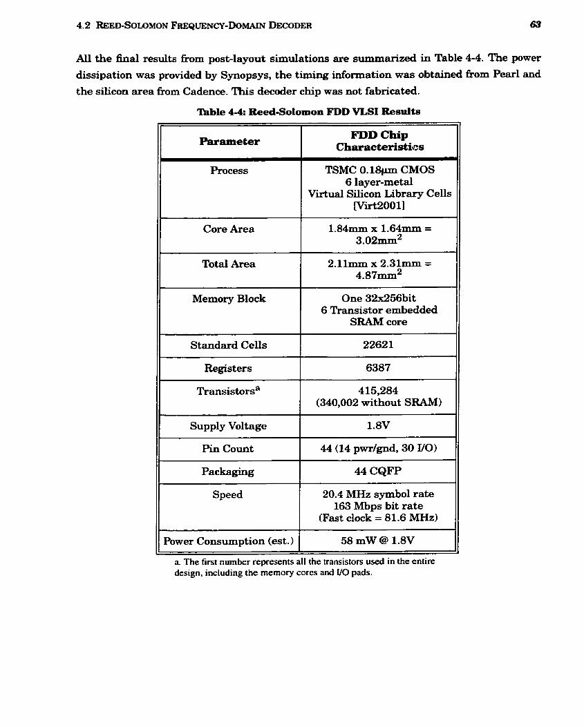
AU the final results fkom post-layout simulations are summarized in Table 4-4. The power
dissipation was provided by Synopsys, the timing information was obtained from Pearl and
the silicon area fiom Cadence. This decoder chip was not fabricated.
Table 4-4: Reed-Solomon FDD VLSI R e d t s
FDD Chip Characteristics
TSMC 0 . 1 8 ~ CMOS 6 layer-metal
Virtual Silicon Library Cells [VirtZOOll
Core Area
Total Area
Mernory Block One 32x256bit 6 Transistor embedded
SRAM core
II Standard Cells 1 22621
II Regist ers I 6387
415,284 (340,002 without SRAM)
II Pin Count 1 44(14p~r/gnd,3OYO)
II Packaging I 44 CQFP
Speed 20.4 MHz symbol rate 163 Mbps bit rate
(Fast clock = 81.6 MHz) - -
Power Consumption (est.) 58 mW @ 1.8V
a. The first number represents al1 the transistors used in the entire design, including the memory cores and if0 pads.
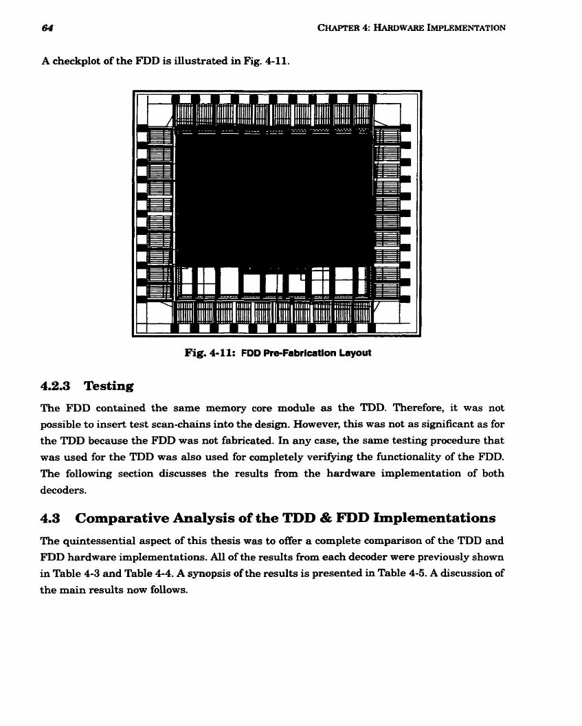
64
A checkplot of the FDD is illustrated in Fig. 4-1 1.
Fig. 4-11: FDD PreFabrication Layout
4.2.3 Testing
The FDD contained the same memory core module as the TDD. Therefore, it was not
possible to insert test scan-chains into the design. However, this was not as significant as for
the TDD because the FDD was not fabricated. In any case, the same testing procedure that
was used for the TDD was also used for completely venfying the functionality of the FDD.
The following section discusses the results h m the hardware implementation of both
decoders.
4.3 Comparative Analysis of the TDD & FDD Implementations
The quintessential aspect of this thesis was to offer a complete cornparison of the TDD and
FDD hardware implementations. Al1 of the results from each decoder were previously shown
in Table 4-3 and Table 4-4. A synopsis of the results is presented in Table 4-5. A discussion of
the main results now follows.
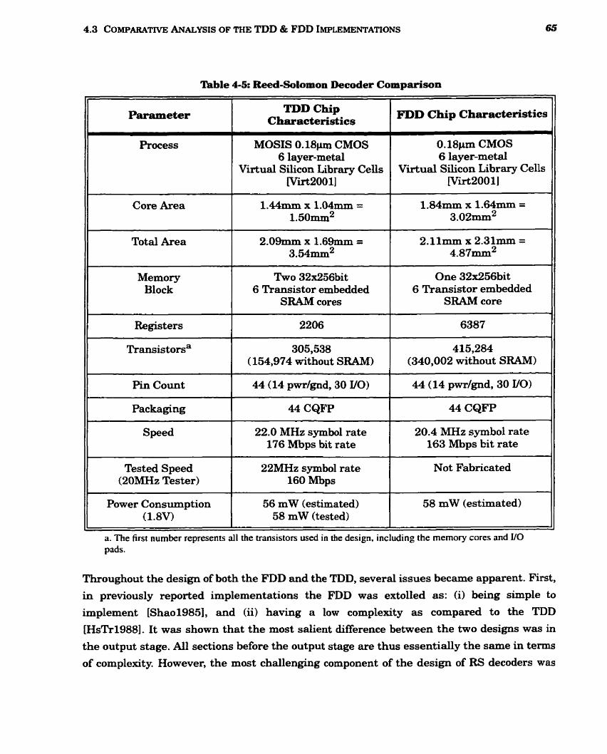
4.3 COMPARATIVE ANALYSIS OF THE TDD & FDD IMPLEMENTATIONS
'iàble 44% Red-Solomon Decoder Cornparison
Parameter - - .-
Rocess MOSIS 0.18pm CMOS 6 layer-met al
Virtual Silicon Library Cells [Vù.t2001]
Core Area 1.44mm x 1.04mm = 1. 50mm2
O.18p CMOS 6 layer-metal
Virtual Silicon Library Cells [virt2001]
Total Area 2.09mm x 1.69mm = 2.11mm x 2.3lmm = 3 .54mm2 4.87mm2
Memory Block
Two 32x256bit 6 Transistor embedded
SRAM cores
One 32~256bit 6 Transistor embedded
SRAM core
Registers 1 2206 1 6387
Transistorsa 305,538 415,284 1 (154,974 without SRAM) 1 (340,002 without SRAM)
Pin Count 1 44 (14 pwrlgnd, 30 I/O) 1 44 (14 pwrlgnd, 30 YO)
Packaging 1 44 CQFP 1 44 CQFP
Speed 22.0 MHz symbol rate 20.4 MHz symbol rate 176 Mbps bit rate 163 Mbps bit rate
Tested Speed 22MHz symbol rate Not Fabricated (20MHz Tester) 160 Mbps
Power Consumption 56 mW (estimated) 58 mW (estimated) (1.8V) 58 mW (tested)
a. The first number represents al1 the transistors used in the design, including the memory cores and VO pads.
Throughout the design of both the FDD and the TDD, several issues becarne apparent. First,
in previously reported implementations the FDD was extolled as: (i) being simple to
implement (Shao19851, and (ii) having a low complexity as compared to the TDD [HsTr1988]. It was shown that the most salient difference between the two designs was in
the output stage. Al1 sections before the output stage are thus essentially the same in terms
of complexity. However, the most challenging component of the design of RS decoders was
found to be the actual decoding a lgor i th , which in this case is the MEA. Both decoders
required the MEA block, so each one is e q u d y as complex up to that point of the output
stage. The complexity of the output stages of the decoders is comparable as well.
Architectures used for the Chien search block in the TDD facilitate the design of the output
block. The output stage of the FDC is trivial to implement, but this simplicity is offset by the
high area requirement. Nevertheless, both the TDD and the FDD have a regular and well
stmctured output stage. The control logic was ascertained to be comparable as well.
Therefore, each of the decoders can be said to have the same degree of design complexity
This is because both approaches contained the MEA, which was found to be the most
diflicult RS decoder block to design efficiently.
In addition, it was discovered that the s ~ N c ~ W ~ of the TDD facilitated the detection of
decoding failures. The structure of the Chien search block allowed the TDD to implement
more criteria for determining if the decoded output codeword sequence was incorrect. This
could be done in mal-time. So when the first symbol was output, the decoderfailure pin
indicated if the current upcoming sequence of codeword symbols was successfully decoded.
However, the output structure of the FDD complicated this procedure. Unfortunately, an
efficient and reliable method for indicating a decoding failure for the FDD could not be found
in the published literature. Hence, the reliability of the decoding failure output signal is
s igdcant ly higher in the TDD.
FinaUy, the VLSI results provided in Table 4-5 indicate that the performance of the decoders
were for the most part quite comparable. Both decoders were designed using the same
0.18gm CMOS standard-ce11 library components and they had the same operating voltage of
1.8V. A low overall power consumption was achieved with both designs, but nonetheless the
TDD was still lower in this aspect of the design. The slightly lower power requirement of the
TDD is believed to be the result of using memory blocks instead of register blocks where
possible.
Both decoders used a memory block for staring the input codeword symbols. The TDD used
an additional memory block to store the results from the Chien search algorithm. This was
done in order to check if there had been a decoder failure. However, this was not required in
the FDD since the inverse transform block immediately required the data from the
remaining error transform block. Using a memory block for the inverse transform block was
not feasible either.
Each decoder was designed to operate at approximately the same speed so that a mesningfid
comparison could be made. However, the TDD still proved to be slightly faster than the FDD.
4.3 COMP.~RAT~VE ANALYSIS OF THE TDD & FDD IMPLEMENTATIONS 67
The TDD and FDD had worst case symbol rates of 22.0 MHz and 20.4 MHz, respectively
Each symbol was &bits, which translated into a TDD bit-rate of 176 Mbps and an FDD bit-
rate of 163 Mbps. The additional latency in the FDD can be contributed to the long
computation times required by its output stage.
Nevertheless, the most conspicuous difference between the decoders is the significantly
higher area r e q d by the FDD implementation. A thorough undertaking to optimize the
FDD in terms of area was attempted. However, even the most minimal area FDD design was
precipitously worse than its TDD counterpart. In fact, the core area of the FDD was more
than double that of the TDD. This was due to the hardware requirements of the output
stages. In the non-optimized design, the FDD needed 2n more registers, 2n-3k-1 less GF
adders, n-k less GF multipliers, and n more constant rnultipliers than the TDD. The extra
registers and constant multipliers in the FDD increase the area substantially. Thus, there is
a signîficant area advantage in terms of implementing a TDD over an FDD as was
foreshadowed by the data in Table 3-1 and Table 4-1. A way to further optimize the output
stage of the FDD beyond IShao19851 and WsTr19881 could not be found, such that it would
more suitable for VIS1 design.
An RS encoder was not considered for this thesis because the encoding of RS codes is
relatively simple. The fundamental arithmetic operation is a polynomial modulo operation
which can be efficiently implemented by a LFSR [Jeon1995]. In addition, the designs in this
thesis targeted a (255,239) RS code because of the numerous applications that used this
code. However, it is believed that the results from this thesis, in terms of the TDD versus the
FDD, could apply to RS codes with smaller n and k values. Different architectures would
nevertheless have to be used for some of the blocks, including the multipliers, if the bit size
of the symbols were different than the current 8-bits. Nonetheless, judging by the
applications listed in Section 2.1 this should not be an issue. The majority of the standards
for RS codes that have been released in the past few years al1 seem to be based on 8-bit
codeword symbols. Most of the optimizations in the literature also target this codeword size.
A use for RS codes larger than (255,239) could not be ascertained from examining the code
stnicture of any practical applications of RS codes.
CMOS process technologies are continually improving and new design issues would have to
be considered for a O.13pm CMOS process. Tirne sharing certain blocks of hardware could
further reduce the die area, and still meet the specifications of the target applications if the
designs were to be implemented in a 0.13pm CMOS process. In addition, the design in this
thesis could have been improved through the use of resowce sharing in Synopsys. This
technique provided a 5.4% redudion in area in the same TDD design used in this thesis.
Hence, possible fiirther reductions in area and power could have k e n achieved if this
optimization was used at the beginnXng of the design process.
This design is for the m ~ s t part operating at its maximum bit rate. Pearl was used to obtain
the critical path timing information for both designs. The critical path for the TDD had a
total delay of 28.71 ns. It occurred in the recursive MEA block shown in Fig. 3-7 fiom
Chapter 3. Conversely, the critical path for the FDD had a total delay of 31.29 ns. It occurred
in the polynomial expansion unit illustrated in Fig. 4-6. There was a control signal called
GO, which had to go to several registers. This signal was responsible for causing the critical
path delay in the FDD.
Therefore, it might be possible through the synthesis process to decrease the speed of the
decoder to try and reduce the die area slightly. Nevertheless, the majonty of the design
emphasis was on the minimization of die area and power reduction. However, if future
applications require more speed, then the design would need to have more parallelism. This
would require different architectures for some of the blocks that minimized the area of the
design at the expense of speed.
In short, in terms of VLSI hardware the TDD defmitely has a more efficient and cost
effective architecture than the FDD. Each kas a comparable degree of design complexity.
However, the TDD was superior in terms of area, speed, power consumption and decoding
failure reliability.
Refemng back to Chapter 2, Table 2-3 presented an RS decoder implementation literature
summary. Revious implementations of RS decoders were discussed in terms of several
performance parameters including area, power and speed. The results fi-om this thesis can
be added to the List and are summarized in Table 4-6. Some of the designs in Table 2-3 do
present an implementation with better normalized area. However, some publications used
full-custom designs, they did not incorporate erasures and they did not accommodate as high
of an RS In,k) code as in the synthesizable designs of this thesis. In addition, the transistor
count is lower in a few designs, but these publications do not include memory blocks in the
transistor count and they do not accommodate as high of an RS (n,k) code as the designs in
this thesis.
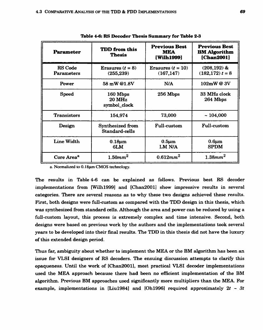
4.3 COMPARATIVE ANALYSIS OF THE TDD & FDD IMPLEMENTATIONS
The results in Table 4-6 can be explained as follows. Revious best RS decoder
implementations from [Wilh1999] and [Chan200 11 show irnpressive results in sever al
categories. There are several reasons as to why these two designs achieved these results.
First, both designs were fÙU-custom as compared with the TDD design in this thesis, which
was synthesized fiom standard cells. Although the area and power can be reduced by using a
fa-custom layout, this process is extremely complex and tirne intensive. Second, both
designs were based on previous work by the authors and the implementations took several
years to be developed into their final results. The TDD in this thesis did not have the luxury
of this extended design period.
Table 4-6: RS Decoder Thesis Summary for Table 2-3
Thus far, ambiguity about whether to implement the MEA or the BM algorithm has been an
issue for VLSI designers of RS decoders. The ensuing discussion attempts to clarifjr this
opaquenesw Unt l the work of [Chan2001], most practical VLSI decoder implementations
used the MEA approach because there had been no efficient implementation of the BM algorithm. Revious BM approaches used significantly more multipliers than the MEA. For
example, implementations in [Liu19843 and [Oh19961 required approximately 2t - 3t
Parameter
RS Code Paramet ers
Power
S ~ e e d
Transistors
Design
Line Width
Core Areaa
a. Normalized to O. 18pm CMOS technology.
TDD h m this Thesis
Erasures (t = 8) (255,239)
58 mW @1.8V
160 Mbps 20 MHz
s ymbol-clock
154,974
Synthesized fkom Standard-ceUs
0.18pm 6LM
1.50mm2
Previous Best MEA
[WilhlsSS]
Erasures (t = 10) ( 167,147)
N/A
256 Mbps
73,000
Full-cust om
0.5pm LM N/A
0.612mm2
Previous Best BM Algorithm [Chan2001 1
(208,192) & (182,172) t = 8
102mW @ 3V
33 MHz clock 264 Mbps
- 104,000 - - -
Full-custom
0.6pm SPDM
1.38nm2
multipliers for the BM algorithm decoding, where t is the number of correctable errors.
However, [Chan20011 developed an iterative time sharing algorithm which essentially made
the VLSI implementation of the BM algorithm comparable to the MEA. The design reduced
the number of finite field multipliers h m 2t - 3t to three multipliers in the decoding
algorithm, which is comparable to the four used in the standard MEA.
In addition, although the BM implementation in [Chan20011 is attractive in terms of its
performance, it does have a drawback because there is a patent on the design. Conversely,
the patent on the MEA has expired and can now be freely implemented by al1 designers.
Furthermore, two independent perspectives corroborate the use of either algorithm. An
algorithmic cornparison was presented in [Saka1995]. The conclusion was that both methods
yield distinct but siinilar parallel architectures with the same optimal complexity T ' e n in
[Chi 19931, the two algorithms were compared in terms of machine cycles. It was ascertained
that both algorithms required the exact same amount of cycles to complete for the syndrome
calculation, key equation, Chien search, error value evaluation and overall decoding.
Finally, the memory requirements can be said to be equivalent for both algorithms. Each one
requires the storage of the input codewords, which will then be used in their respective
output stages to form the decoded codewords. Therefore, these two algorithms can be said to
be equivalent, and the choice to implement one versus the other becomes a matter of
personal preference for the RS decoder designer.
4.4 Summary
The contributions of this chapter are as follows.
An optimized Reed-Solomon TDD and FDD were constructed using a combination of
area-efficient and low power VLSI architectures.
Two RS decoders were designed and built in a 0.18pm CMOS standard-cell technology.
The TDD was fabricated.
An FDD and a TDD were analyzed and compared in terms of their respeded VLSI
hardware implementations with the following results: - The decoding algorithm, in this case the MEA, is the largest contributor to design complexity. Each decoder is essentially identical up to and including the Ml?,A. Therefore, the decoders are comparable in design and implementation complexity.
The TDD was proven to be superior to the FDD because the TDD chip had a smaller area, faster decoding speed, lower power consumption and a more reliable decoder failure indicator.
* The prohibitive area of the FDD was its most prominent limitation to practical applications. - The BM algorithm and the MEA are essentially identical, and the choice as to which one
should be implemented for an RS decoder is arbitrary.
The next chapter presents the results from the C code implementation of both RS decoders
for use in embedded software applications.

Chapter H Software Implementation
The previous chapter discussed the hardware implementations of the TDD and the FDD.
Chapter 5 now presents the results obtained from implementing each decoder in s o h e
using C code. The purpose of this section is to present a straightforward software
comparison of the two decoders for the sake of thoroughness. This approach was intended to
determine which decoder would be more suitable in a system containing an embedded
processor core that is part of a larger SOC implementation.
There were several important parameters from the software implementation that needed to
be obtained for comparing the two decoders. The executable size of the program and static
memory allocation were of special interest to this thesis. Processor cores are small and the
memory area dominates the overall die area in SOC implementations. For the sake of design
expediency, no dynamic memory allocation was used in this implementation of RS decoders.
Hence there was a slight loss in efficiency, but the reduction in design complexity offset this
loss. In addition, the various computing times required by each decoder block were
compared. This information would determine the specific blocks that had the highest
computational requirements. Finally, several compiler optimization options were used to
obtain the most efficient RS decoder software implementation.
5.1 System Specifications
The fiinctionality of the (255,239) RS codes for both the TDD and FDD were verified through
exhaustive simulations. Several hundred thousand test codewords and various error and
erasure combinations were used in these simulations for both decoders.
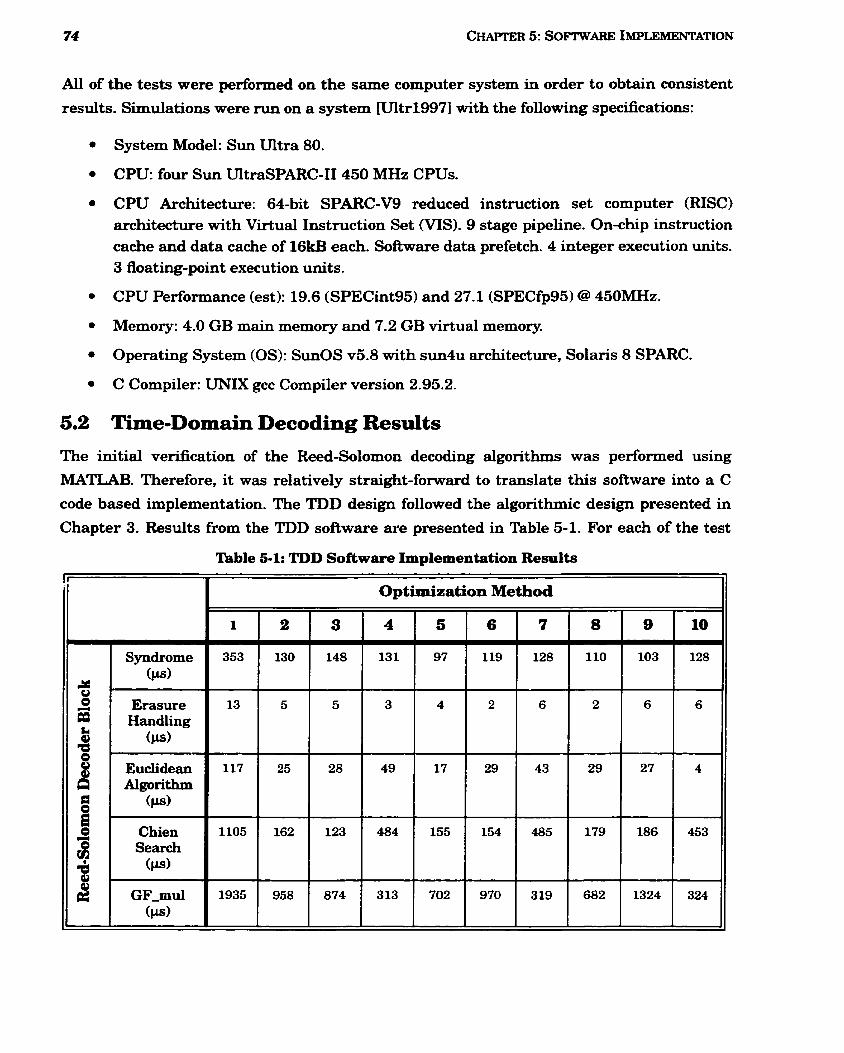
Al1 of the tests were performed on the same computer system in order to obtain consistent
results. Simulations were run on a system [Ultr1997] with the following specifications:
System Model: Sun Ultra 80.
CPU: four Sun UltraSPARC-II 450 MHz CPUs.
CPU Architecture: 64-bit SPARC-V9 reduced instruction set computer (RISC) architecture with Virtual Instmction Set (VIS). 9 stage pipeline. On-chip instmction cache and data cache of 16kB each. Software data prefetch. 4 integer execution units. 3 floating-point execution units.
CPU Performance (est): 19.6 (SPECint95) and 27.1 (SPECfp95) @ 450MHz.
Memory: 4.0 GB main memory and 7.2 GB virtual memory.
Operating System (OS): SunOS v5.8 with sun4u architecture, Solaris 8 SPARC.
C Compiler: UNIX gcc Compiler version 2.95.2.
Time-Domain Decoding Results
The initial vedcation of the Reed-Solomon decoding algorithms was performed using
MATLAB. Therefore, it was relatively straight-forward to translate this software into a C
code based implementation. The TDD design followed the algorithmic design presented in
Chapter 3. Results from the TDD software are presented in Table 5-1. For each of the test
mble 5-1: TDD Software Implementation Results
Optirnization Method
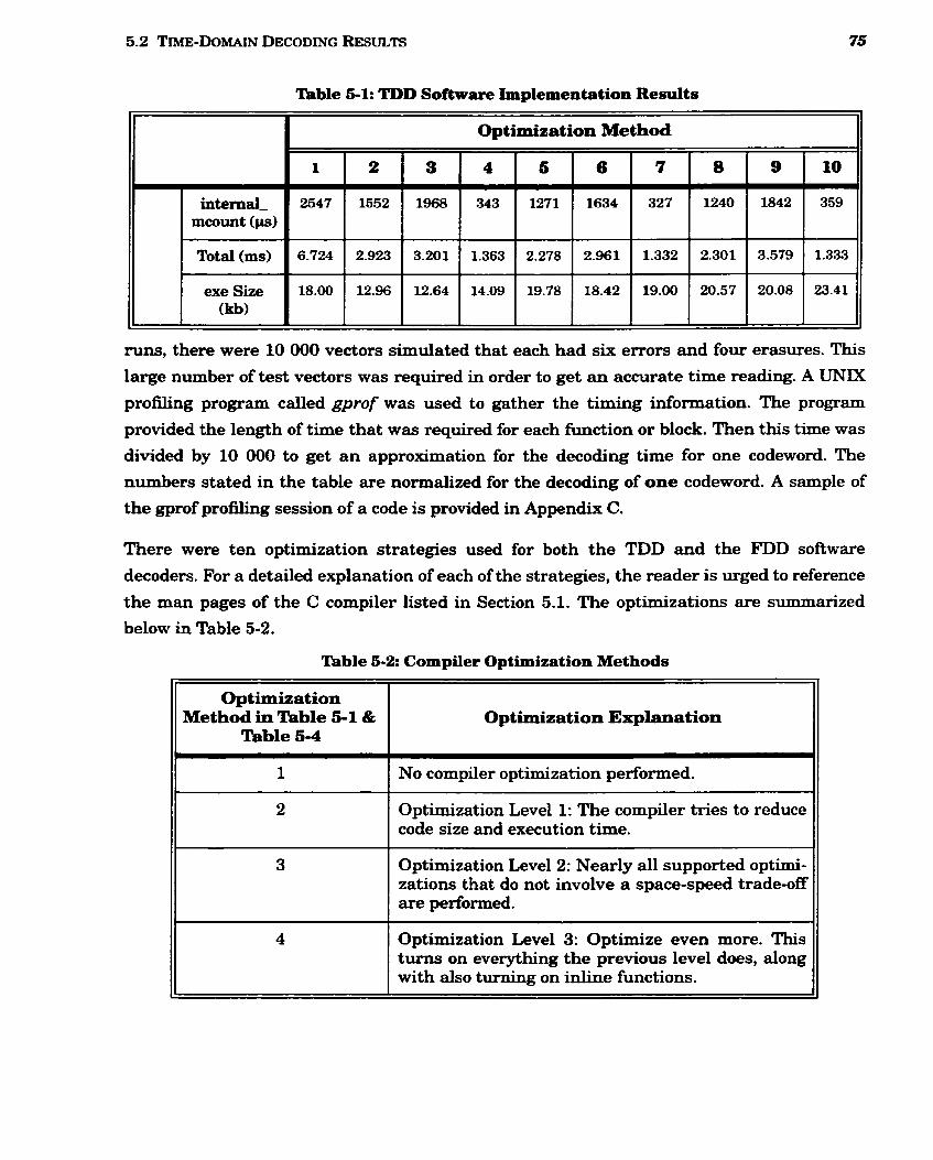
'hble 5-1: TDD Sofhvai.e Implementation Results
II I Optimization Method II
-
runs, there were 10 000 vectors simulated that each had six errors and four erasures. This
large number of test vectors was required in order to get an accurate tirne reading. A U N E
profiling program called gprof was used to gather the timing information. The program
provided the length of time that was required for each function or block. Then this time was
divided by 10 000 to get an approximation for the decoding time for one codeword. The
numbers stated in the table are normalized for the decoding of one codeword. A sample of
the gprof profiling session of a code is provided in Appendix C.
intemai_ mcount (ps)
Total (ms)
exe size (W
There were ten optimization strategies used for both the TDD and the FDD software
decoders. For a detailed explanation of each of the strategies, the reader is urged to reference
the man pages of the C compiler listed in Section 5.1. The optimizations are s-arized
below in Table 5-2.
1 No compiler optimization performed.
9
1842
3.579
20.08
8
1240
2.301
20.57
1
2547
6.724
18.00
Table 5-2: Compiler Optimization Methods
Optimization Level 1: The compiler tries to reduce code size and execution time.
10
359
1.333
23.41
Optimization Method in Table 5-1 &
Table 5-4
Optimization Level2: Nearly al1 supported optimi- zations that do not involve a space-speed trade-off are performed.
2
1552
2.923
12.96
Optimization Explanation
Optimization Level 3: Optirnize even more. This turns on everything the previous level does, dong with also turning on inline functions.
3
1968
3.201
12.64
7
327
1.332
19.00
4
343
1.363
14.09
6
1271
2.278
19.78
6
1634
2.961
18.42
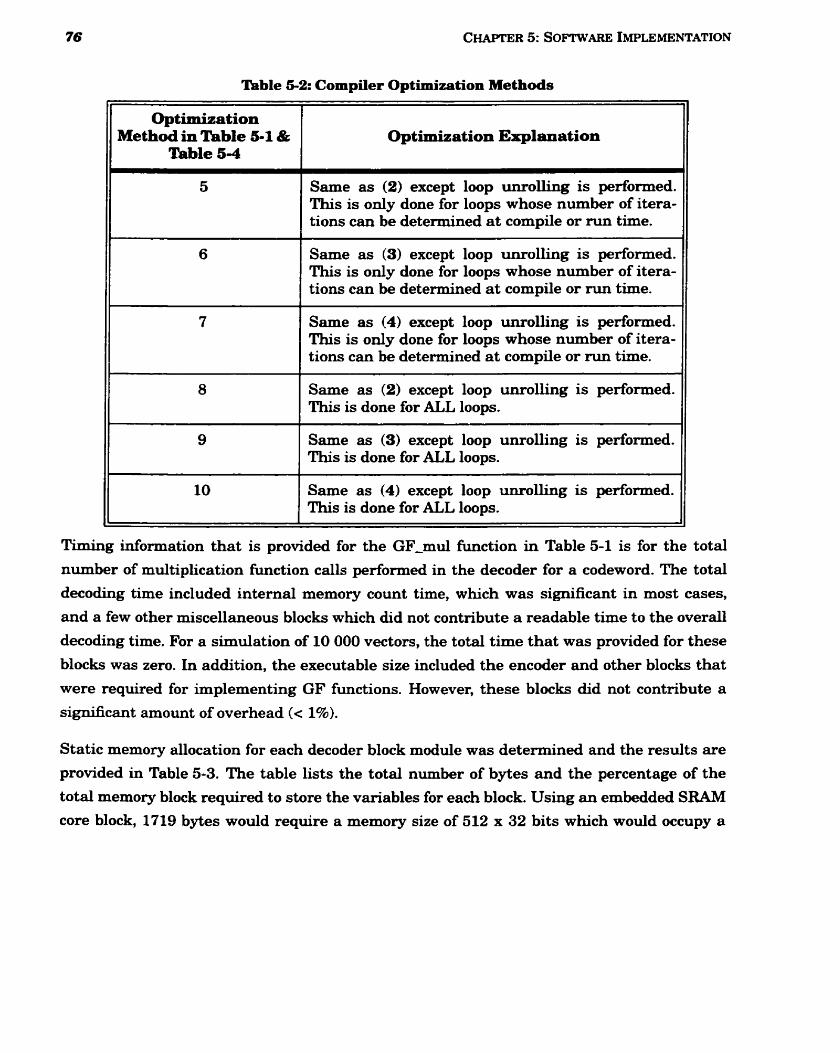
Same as (2) except loop unrolling is performed. This is only done for loops whose number of itera- tions can be determined at compile or run time.
Table 5-2: Compiler Optimization Methods
Same as (3) except loop unrolling is performed. This is only done for loops whose number of itera- tions can be determined at compile or run time.
Optimization Method in Table 5-1 &
Table 5-4
II 7 1 Same as (4) except loop unrolling is performed.
Optimization Exphnation
This is only done for loops whose number of itera- tions can be determined a t compile or run tirne.
Same as (2) except loop unrolling is performed. This is done for ALL loops.
Same as (3) except loop unrolling is performed. This is done for ALL loops.
'Piming information that is provided for the GF-mul function in Table 5-1 is for the total
number of multiplication function calls performed in the decoder for a codeword. The total
decoding time included interna1 memory count time, which was significant in most cases,
and a few other miscellaneous blocks which did not contribute a readable time to the overall
decoding time. For a simulation of 10 000 vectors, the total time that was provided for these
blocks was zero. In addition, the executable size included the encoder and other blocks that
were required for irnplementing GF functions. However, these blocks did not contribute a
significant amount of overhead (< 1%).
10
Static memory allocation for each decoder block module was determined and the results are
provided in Table 5-3. The table lists the total number of bytes and the percentage of the
total memory block required to store the variables for each block. Using an embedded SRAM core block, 1719 bytes would require a memory size of 512 x 32 bits which would occupy a
Same as (4) except loop unrolling is perforxned. This is done for ALL loops.
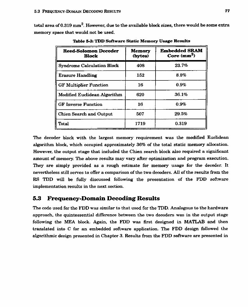
total area of 0.3 19 mm2. However, due to the available block sizes, there would be some extra
memory space that would not be used.
The decoder block with the largest memory requirement was the modified Euclidean
algorithm block, which occupied approximately 36% of the total static memory allocation.
mble 5% TDD Software Static Memory Usage ResuIts
However, the output stage that included the Chien search block also required a significant
amount of memory. The above results may vary after optimization and program execution.
Embedded SRAM Core (mm2)
23.7%
8.8%
0.9%
36.1%
0.9%
29.5%
0.319
Reed-Solomon Decoder BIock
1 Syndrome Calculation Block
Erasure Handling
GF Multiplier Function
Modified Euclidean Algorithm
GF Inverse Fundion
Chien Search and Output
Total
They are simply provided as a rough estimate for memory usage for the decoder. It
nevertheless still serves to offer a comparison of the two decoders. Al1 of the results fiom the
RS TDD will be fully discussed following the presentation of the FDD software
Memory (bytes)
408
152
16
620
16
507
1719
implementation results in the next section.
5.3 Frequency-Domain Decoding Results
The code used for the FDD was similar to that used for the TDD. Analogous to the hardware
approach, the quintessential ciifference between the two decoders was in the output stage
following the MEA block. Again, the FDD was first designed in MATLAB and then
translated into C for an embedded software application. The FDD design followed the
algorithmic design presented in Chapter 3. Results from the FDD software are presented in
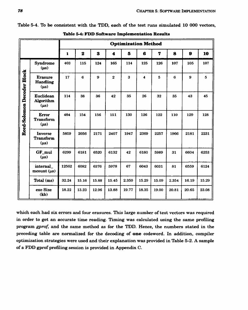
78 CHAPTER 5: SOFTWARE IMPLEMENTATION
Table 5-4. To be consistent with the TDD, each of the test runs simulated 10 000 vectors,
Table 5-4: FDD Software Implementation Results
Erasure Handling
(w)
Euclidean Algorithm
(w)
Inverse Transform
(w)
intemal- mcount (ps)
Total (ms)
Optimization Method
which each had six errors and four erasures. This large number of test vectors was required
in order to get an accwate time reading. Timing was calculated using the same profiling
program gprof, and the same method as for the TDD. Hence, the numbers stated in the
preceding table are normalized for the decoding of one codeword. In addition, compiler
optimization strategies were used and their explanation was provided in Table 5-2. A sample
of a FDD gprof profiling session is provided in Appendix C.
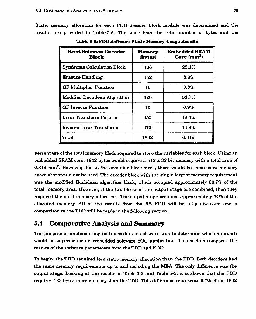
5.4 COMPARATIVE ANALYSE AND SUMMARY 79
Static memory allocation for each FDD decoder block module was determined and the
results are provided in Table 5-5. The table lists the total number of bytes and the
Ikible 6-5: FDD Software Static Memory Usage Results
Syndrome Calculation Block 1 408 1 22.1% I
Reed-Solomon Decoder Block
Erasure Handling 1 152 1 8.3% 1 GF Multiplier Function 1 l6 1 0.9% I
Memory (bytes)
Embedded SRAM tore (mm2)
GF Inverse Function
Error Transform Pattern
Inverse Error Transforms
percentage of the total memory block required to store the variables for each block. Using an
embedded SRAM core, 1842 bytes would require a 512 x 32 bit memory with a total area of
0.319 mm2. However, due to the available block sizes, there would be some extra memory
space tkst would not be used. The decoder block with the single largest memory requirement
was the mot-Xîed Euclidean algorithm block, which occupied approximately 33.7% of the
total memory area. However, if the two blocks of the output stage are combined, then they
required the most memory allocatior;.. The output stage occupied approximately 34% of the
allocated memory. AI1 of the results from the RS FDD will be M y discussed and a
comparison to the TDD will be made in the following section.
1 1
16
-- --
Total
5.4 Comparative Analysis and Summary
0.9%
355
275
The purpose of implementing both decoders in software was to determine which approach
would be superior for an embedded software SOC application. This section compares the
results of the software parameters from the TDD and FDD.
19.3%
14.9%
1842
To begin, the TDD required less static memory allocation than the FDD. Both decoders had
the same memory requirements up to and including the MEA. The only difference was the
output stage. Looking at the results in Table 5-3 and Table 5-5, it is shown that the FDD
requires 123 bytes more memory than the TDD. This difference represents 6.7% of the 1842
0.319

total bytes required by the FDD. The variance is entirely due to the large mernory required
for the error transform output stage of the FDD. In fact, this was the same issue that
plagued the FDD hardware implementation. Hence, it can be said that the TDD is more
efficient in terms of memory usage.
Executable size of the entire Reed-Solomon program was compared. Again, the TDD was
vastly superior to the FDD. To elaborate, each decoder was able to achieve a minimum
executable size of 12.96kbytes through the use of various compiler optimization options.
However, the decoding times for the TDD and the FDD were 2.923111s and 15.88ms,
respectively. For the same area, the FDD was over five times as slow as the TDD. The source
of the rather large latency in the FDD was the inverse transform block. It becomes
unquestionably clear then, that the TDD is the decoder of choice for trying to achieve a more
compact and thus cost-effective embedded software implementation.
F'indy, the decoding times of each of the decoders were compared. Once again the FDD was
proved to be inferior to the TDD. For most of the results, the FDD perfonned drarnatically
worse than the TDD. However by unrolling loops in the code, the compiler was able to devise
a relatively fast implementation of the FDD. Nonetheless, the fastest FDD a t 2.35ms was
still twice as slow when compared to the fastest TDD at 1.332111s. These times correspond ta
decoding speeds of 868kpbs for the FDD and 1.53Mbps for the TDD on the given CPU. The
TDD even had a smaller executable size than the FDD at these speeds. Table 5-1 and
Table 5-4 show that the executable sizes for the faster TDD and FDD are 19.00kbytes and
19.77kbytes, respectively. In short, the TDD is undoubtedly more efficient for SOC
applications in terms of rninimizing executable size.
The most significant problem with the FDD approach, that caused such a precipitous
degradation in performance, was the inverse transform block. It was computationally
intensive and required s i g d c a n t memory allocation. As an analogy, the inverse transform
block can be considered as being the Achilles heel of fiequency-domain RS decoding. There
have been essentidy no proposais in the literature to ameliorate this issue. It seems then
that the algorithrnic structure of the output block makes it difficult to design a practical
implementation of the FDD.
In terms of design complexity, the two decoders were found to be almost equivalent. The
design of the decoders is essentially the same up to their respective output stages.
Nevertheless, the most complicated aspect of decoding is the MEA decoding algorithm,
which is present in both implementations. The output stage of the FDD is slightly more
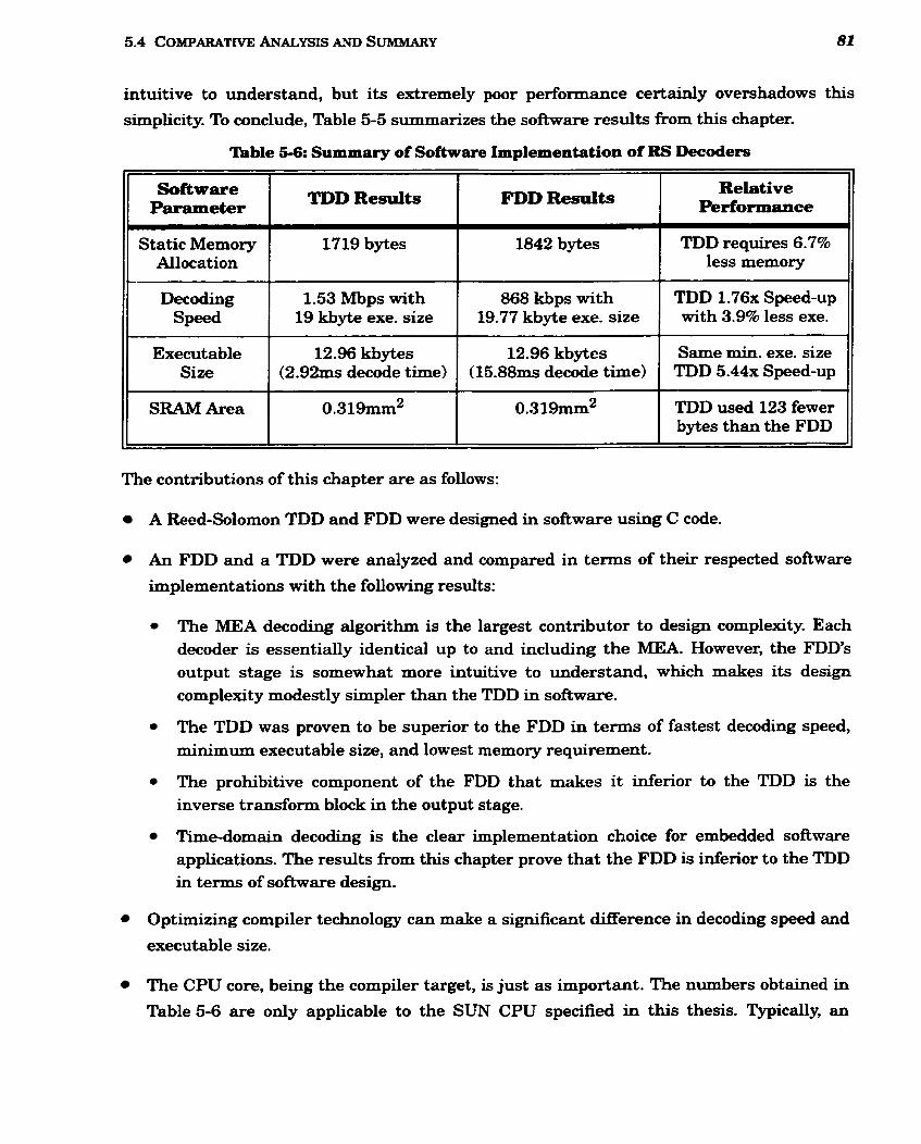
5.4 COMPARAT~VE ANALYSIS AND SUMMARY 81
intuitive to understand, but its extremely poor performance certainly overshadows this
simplicity. To conclude, Table 5-5 summarizes the software results from this chapter.
Table 5-6: Summary of Software Implementation of RS Decoders
Static Memory Allocation
Software 1 TDD Results Parameter - - -- - - -
1719 bytes
Relative Performance
- -
1842 bytes TDD requires 6.7% less memory
- -- .-
Decoding 1.53 Mbps with 19 kbyte exe. size
868 kbps with 19.77 kbyte exe. size
TDD 1 . 7 6 ~ Speed-up with 3.9% less exe.
Executable Size
12.96 kbytes (292x11s decode tirne)
12.96 kbytes (15.88ms decode time)
The contributions of this chapter are as follows:
Same min. exe. size TDD 5 . 4 4 ~ Speed-up
SRAM Area
A Reed-Solomon TDD and FDD were designed in software using C code.
An FDD and a TDD were analyzed and compared in terms of their respected sofiware
implementations with the following results:
0.319mm2
The MEA decoding algorithm is the largest contributor to design complexity. Each decoder is essentially identical up to and including the MEA. However, the FDD's output stage is somewhat more intuitive to understand, which makes its design complexity modestly simpler than the TDD in software.
The TDD was proven to be superior to the FDD in te- of fastest decoding speed, minimum executable size, and lowest memory requirement.
0.3 19mm2
The prohibitive component of the FDD that makes it iderior to the TDD is the inverse transform block in the output stage.
TDD used 123 fewer bytes than the FDD
Time-domain decoding is the clear implementation choice for embedded software applications. The resdts from this chapter prove that the FDD is inferior to the TDD in terms of s o h a r e design.
Optimizing compiler technology can make a significant clifference in decoding speed and
executable size.
The CPU core, being the compiler target, is just as important. The numbers obtained in
Table 5-6 are only applicable to the SUN CPU specified in this thesis. Typically, an

ARM7 or -9 CPU would be used and the exact same numbers cannot be expected for
either of these irnplementations.
The concluding chapter is presented next.

Chapter rn Conclusions
This thesis examined Reed-Solomon tirne-domain and fkequency-domain decoder
implementations in s o h e and hardware. The focus was on designing an area-efficient,
low-power and low-complexity RS decoder.
Chapter 2 discussed the basics of error correction codes, including Reed-Solomon codes. The
prolific use of RS decoders was c o h e d by presenting some of the applications that use RS
codes. In addition, decoding algorithms were presented and the reasoning of why the MEA was chosen for this thesis was defended. Finally, an extensive review of the literature
pertairùng to RS codes, decoders, and mathematics was presented. It showed that there are
no cornparisons of VLSI implementations of RS TDDs and FDDs that provide a definitive
encompassing statement about the merits of either decoder in VLSI. This served as the
primary motivation for the work presented in this thesis.
In chapter 3, the theory and arithmetic behind the design of an RS decoder was presented.
AU of the required equations for decoding in the tirne-domain or the frequency-domain were
explained. In addition, each decoder was partitioned into its constituent blocks. Each block
was then fùlly explained and block diagrams were provided to illustrate how to realize
various equations in hardware. It was shown that both decoders were for the most part quite
similar in architecture. However, the quintessential difference between the two was in the
structure of the output stage.
Chapter 4 presented the hardware implementation of the RS decoders. The TDD was
presented first and its architectural modifications were discussed. Various architectures
were combined in order to achieve the most optimal design in terms of area and power
consumption. It was shown that the design complexity was reduced s igdcant ly fiom
previous approaches. The results from testing the hal TDD ASIC design were also
presented. Subsequently, the FDD design was discussed and its results were illustrated.
Most important, the VLSI results from the two decoder implementations were compared and
contrasted. This showed that the decoders are similar in terms of design complexity. The
TDD was slightly better in terms of power consumption and decoding speed. Nonetheless,
the FDD was found to be drastically inferior to the TDD in terms of area usage. The FDD
had double the area compared to the TDD. Actual VLSI results corroborated the definitive
statements made in this chapter.
In chapter 5, the sofkware implementation of the two RS decoders was docwnented. The
purpose of comparing the two decoders in software was to ascertain which approach would
be better suited for use in a SOC realization. Hence, the areas that were examined were the
executable size, static memory allocation and decoding speed. In all areas, the TDD
performed s igdcant ly better than the FDD. The only advantage to using an FDD was that
its output stage was more intuitive to understand. Nonetheless, this was not the most
complex block in the decoder. In both cases, the block with the highest design complexity was
the MEA. Finally, the degradation in performance of the FDD was attributed to the
inefficiency of the inverse transforxn block.
6.2 Conclusions
Reed-Solomon decoders were shown to errist in a multitude of practical applications, thus
establishing the need for performing further research in this area. Thus far, ody ambiguous
and uncorroborated statements about R S decoder implementations have been made.
Virtually no remarks have been made on deep submicron (DSM) implementations
synthesized from HDL. Based on the results from this thesis, the following definitive
statement s serve to clarify this ambiguity.
Time-domain RS decoding is a better approach for VLSI implementations than frequency-
domain decoding. The FDD has double the silicon area for a slower decoding speed than the
TDD. Power consumption is shown to be quite similar, with the TDD requiring slightly less
power than the FDD. Moreover, the two decoders are comparable in terms of design
complexity. Each decoder is essentially the same up to and including the decoding algorithm,
which was the most complicated block of the decoder. Hence based on the VLSI results, it is
6.4 FUTURE RESEARCH 85
said with unequivocal confidence that the TDD is superior to the FDD for hardware
applications.
In terms of software, the TDD is superior to the FDD. The TDD required less memory, had
faster decoding speeds and had smaller executable sizes than the FDD. However, the only
merit of the FDD was that its output stage was more intuitive to understand. It was
ascertained that the detrimental factor of the FDD was the inverse transform block of the
output stage. This block clearly degraded the FDD's performance such that it made the TDD the only feasible choice for software-based applications.
6.3 Contributions of this Thesis
The contributions of this thesis were:
The presentation of a review of RS decoder literature, which up to this point has been ambiguous about which decoder approach (TDD or FDD) is superior.
A low-power, low-complexity and area optimized Red-Solomon decoder architecture for both a tirne-domain and a frequency-domain implementation.
A O.18pm ASIC implementation of the optimized RS TDD synthesized fiom a Verilog HDL description.
Definitive statements comparing the TDD and FDD in both hardware and software.
Future Research
The search for more efficient algorithrns, faster design times, and better implementations is
a continual process. Whether it be from market demands or personal ambition,
improvements over previous approaches will always be attempted. The field of Reed-
Solomon decoder VLSI design is no exception. Hence, there are still several unanswered
questions that remain and are thus open for fiiture research.
6.4.1 Reed-Solomon Decoding Algorithms
Although hard-decision decoders dominate VLSI RS error correction applications, there are
theoretically more efficient and powerfd decoders. These are the algebraic soft-decision
decoders [Koet2000] that are able to provide a lower BER at a given SNR. However, their
complexity makes practical VLSI implementation prohibitively difficult at this time.
Research into deriving algorithnis that are suitable for VLSI design is currently under way.
6.45 ASIC Design Methodology and Flow
ASIC design methodology and flow becomes an integral issue with increasing time-to-
market demands. Moore's Law states that approximately every eighteen to twenty-four
months the number of transistors per unit of die area doubles, so new design flows must be
developed and utilized quickly. The learning cume is precipitous and this considerably
increases the design tirne. Moreover, bugs in the design Aow cause a greater effort to be
placed on debugging the vendor tools rather than on the design itself.
In an academic setting, i t would be beneficial to have ASIC designers work in parallel while
proceeding through the new design flow. This way, these researchers could collaborate and
discuss design flow issues when they accu. Design time could be reduced and the focus of
academic ASIC design could be placed back on the design and not on constmcting a design
flow.
6.4.3 Galois Field Architecture Cornparisons
When designing an ASIC at the RTL design stage, it can be quite difEcult to be able to
predict desiw parameters such as proposed area, timing and power consumption. Therefore,
it would be interesting if a chart of data could be constructed that provided preliminary
information about these design parameters. A designer could simply count up how many
registers, memory cells, and GF arithmetic structures there were in the design to get a lower
bound estimate of the chip's performance.
Constmcting this chart of data for GF arithmetic structures would be straightforward.
Variable bit multipliers, adders and inverters would be synthesized from their respected
HDL codes. Then each component would be placed, routed and verified. At that point,
numbers for power consumption, timing and area could be ascertained. Findly, the designer
could reference these nwnbers and estimate the ASIC's performance based on the number of
components in the design.
References [AHA2000]
[Berl 19681
[Berl19861
[Berl 19871
[Berl 19891
[Blah1979]
IBurt 197 11
[Chan19981
[ChSh1999]
[Chan19991
[ChSu19991
[Chan200 11
Advanced Hardware Architectures (AHA) Inc., "http: / / www.aha.com / Publications /pb4013b-0600.pdf", 2000.
E. R. Berlekamp, Algebraic Coding Theory, New York: McGraw-Hill, 1968. (Revised edition, Laguna Hills: Aegean Park Press, 1984).
E. R. Berlekamp, and L. R. Welch, "Error Correction for Algebraic Block Codes," US. Patent US4633470,1986.
E. R. Berlekamp, R. E. Peile, and S. P. Pope, The Application of Error Control to Communication," IEEE Comm. Magazine, vol. 25, pp. 44-57, 1987.
E. R. Berlekamp, "Soft Decision Reed-Solomon Decoder," US. Patent US4821268,1989.
R. E. Blahut, "Transform Techniques for Error Control Codes," ZBM Journal of Research and Development, vol. 23, pp. 299-315, 1979.
H. O. Burton, "Inversionless Decoding of Binary BCH Codes," IEEE Trans., vol. IT-71, pp. 464-466, 1971.
H. -C. Chang, and C. B. Shung, "A(208,192;8) Reed-Solomon Decoder for DVD Application," IEEE Int. Conference on Communications, vol. 2, pp. 957-960, June 1998.
H. -C. Chang, and C. B. Shung, "New Serial Architecture for the Berlekamp- Massey Algorithm," IEEE Trans. on Communications, vol. 47, issue 4, pp. 481- 483, A p d 1999.
H. Chang, and M. H. Sunwoo, "A Low-Complexity Reed-Solomon Architecture Using the Euclid's Algorithrn," IEE'E Proc. of the International Symposium on Circuits and Systems, ISCAS '99., vol. 1, pp. 513-516, May 1999.
W. Chang, and M. H. Sunwoo, "Design of an Area Efficient Reed-Solomon Decoder ASIC Chip", IEEE Workshop on Signal Processing Systems, 1999. SiPS 99., pp. 578-585, Oct. 1999.
H. -C. Chang, C. B. Shung, and C. -Y. Lee, "A Reed-Solomon Product-Code (RS- PC) Decoder Chip for DVD Applications," IEEE Journal of Solid-State Circuits, vol. 36, issue 2, pp. 229-238, Feb. 2001.
[Chen19951 H. -W. Chen, J. -C. Wu, G. -S. Huang, J. -C. Lee, and S. -S. Chang, "A New VLSI Architecture of Red-Solomon Decoder with Eraswe Function," IEEE Global Telecornmunications Conference, GLOBECOM '95., vol. 2, pp. 1455-1459, Nov. 1995.
[Chi19931 D. Chi, "A New Fast Reed-Solomon Decoding Algorithm Without Chien Search," IEEE Conference Record of Cornmunications on the Moue, vol. 3, pp. 948-952, Oct. 1993.
[Chie19641 R. T. Chien, "Cyclic Decoding Procedure for the Bose-Chaudhuri- Hocquenghem Codes," IEEE Bans. on Information Theory, vol. IT-10, pp. 357- 363, Oct. 1964.
[Cho019921 S. Choomchuay, and B. Arambepola, "An Algorithm and a VLSI Architecture for Reed-Solomon Decoding," IEEE Proc. of the International Symposium on Circuits and Systerns, ISCAS '92., vol. 5, pp. 2120-2123, May 1992.
[Coop2000] 1. R. Cooper, and M. A. Bramhall, "ATM Passive Optical Networks and Integrated VDSL," ZEEE Comm. Magazine, vol. 38, issue 3, pp. 174-179, March 2000.
[Core2000] CorePool, "http: / / www.corepool.com /products lfhg_rs-dec. htm", 2000.
[Cost1998] D. J. Costello Jr., J. Hagenauer, H. Irnai., and S.B. Wicker, "Applications of Error-Control Coding," IEEE Zkans. on Inform. Theory, vol. 44 no. 6, Oct. 1998, pp. 2531-2560.
[Dabi1995] D. Dabiri, and 1. E Blake, "Fast Parallel Algorithms for Decoding Reed- Solomon Codes Based on Remainder Polynomials," IEEE Tkans. on Information Theory, vol. 41, no. 4, pp. 873-875, July 1995.
[Dutt 19991 A. Dutta-Roy, "Networks for Homes", IEEE Spectrurn, vol. 26, issue 9, pp. 26- 33, Dec. 1999.
[eMDT2000] e-MDT Inc. ,''http: / / www.e-rndt.com /communication.Atm", 2000.
[ETSI20011 ETSI standard, "Transmission and Mult iplehg (TM); Access transmission systems on metallic access cables; Very high speed Digital Subscriber Line (VDSL); Part 2: Transceiver specification," ETSI TS 101 270-2 VI. 1.1,2001.
[Fitz1998] P. Fitzpatrick, and S. M. Jennings, "Cornparison of Two Algorithms for Decoding Alternant Codes," Applicable Algebra in Eng., Commun., and Computing, vol. 9, pp. 211-220, 1998.
[Forn1965] G. D. Forney, "On Decoding BCH Codes," IEEE Pans. on Information Theory, vol. IT-11, pp. 549-557, Oct. 1965.
[4i2i2000] 4i2i Communications Ltd., http: / / w ww. disi. corn / reed-solomon-codes. htm, 2000.
[Gore1961] D. Gorenstein, and N. Zierler, "A Class of Error Correcting Codes in pm Symbols," Journal of the Society of Industrial and Applied Mathernatics, vol 9., pp. 207-214, June 1961.

[Guo 19981
[Lin19831
[Liu 19841
J. -H. Guo, and C. -L. Wang, "Hardware-efficient Systolic Architecture for Inversion and Division in GF(2m)," IEE Proc. on Computers and Digital Techniques, vol. 145, no. 4, pp. 272-278, July 1998.
1. S. Hsu, T. K. TRiong, L. J. Deutsch, E. H. Satorious, and 1. S. Reed, "A Comparison of VLSI Architectures for Time and Transform Domain Decoding of Red-Solomon Codes," Jet Ropulsion Laboratory, Pasadena, CA, TDA Progress Rep. 42-92, Oct-Dec. 1989, pp. 63-81, J a n 1988.
1. S. Hsu, T. K. Truong, L. J. Deutsch, and I.S. Reed, "A Comparison of VLSI Architecture of Finite Field Multipliers Using Dual, Normal, or Standard Basis," IEEE Dans. on Computers, vol. 37, no. 6, June 1988.
J.- M. Hsu, and C.-L. Wang, "An Area-Efficient VLSI Architecture for Decoding of Reed-Solomon Codes," IEEE Int. Conference on Acoustics, Speech and Signal Processing, vol. 6, pp. 3291-3294, May 1996.
J. -C. Huang, C. -M. Wu, M. -D. Shieh and C. -H. Wu, "An Area-Efficient Versatile Reed-Solomon Decoder for ADSL," IEEE Proc. of the 1999 International Symposium on Circuits and Systerns, ISCAS '99., vol. 1, pp. 517- 520, June 1999.
ITU Draft Recommendation G.992.2 G.lite Standard, http: / / www. itu. int / itudoc / itu-t /rec /glg800up /g-992.2. htrnl, 1999.
J. H. Jeng, J. M. Kuo, and T. K. Truong, "A High Efficient Multiplier for the RS Decoder," International Symposium on VZSI Technology, Systems, and Applications, pp 116-118, June 1999.
J. H. Jeng, and T. K. Truong, "On Decoding of Both Errors and Erasures of a Reed-Solomon Code Using an Inverse-Free Berlekamp-Massey Algorith," IEEE Trans. Commun., vol. 47, pp. 1488-1494, Oct. 1999.
S. M. Jennings, and J. Kessels, "Comparison of the VIS1 CosüPerformance Properties of Two Reed-Solomon Decoding Algorithms," Integration the VZSZ Journal, vol. 25, pp. 103-110, Jwie 1998.
Y. Jeong, and W. Burleson, "High-Level Estimation of High-Performance Architectures for Reed-Solomon Decoding," IEEE Int. Symposium on Circuits and Systems, vol. 1, pp. 720-723, May 1995.
R. Koetter, and A. Vard3r, "Algebraic SoR-Dwision Decoding of Reed-Solomon Codes," Laboratoire I3S, C.N.R.S., France Paper, May 2000.
S. Kwon, and H. Shin, "An Area-efficient VLSI Architecture of a Reed-Solomon Decoder/Encoder for Digital VCRs," IEEE Dans. on Consumer Electronics, vol 434, pp. 1019-1027, NOV. 1997.
S. Lin, and D. Costello, Error Control Coding, Prentice-Hall, 1983.
K. Y. Liu, "Architecture for VLSI Design of Reed-Solomon Decoders," IEEE lYans. Computers, vol. C-33. pp. 178-179, Feb. 1984.
[Shao 19851
LSI Logic Corp., "h'http: 1 1 www.Zsi2ogic.com 1 techlib Itechdocs 1 digi*tal-tu 1 CableModen / 777ds3.pdf", 2000.
J. L. Massey, "Shift Register Synthesis and BCH Decoding," IEEE Trans. on Information Theory, vol. IT-15, no. 1, pp. 122-127, Jan. 1969.
Mitsubishi M64403FP IC datasheet, http: 1 1 www.mitsubishichips.com /data 1 datashets lassps Iassppdflds 1 rn64403e.pa 1999.
Y. U. Oh, and D. Y. Kim, "Method and Apparatus for Computing Error Locator Polynomial for use in a Reed-Solomon Decoder," US. Patent 4 663 470,1996.
K. Oh, and W. Sung, Efficient Reed-Solomon Decoder VLSI with Erasure Correction," 1997 lEEE Workshop On, Signal Processing Systems, 1997.SZPS 97 - Design and Implementation, pp. 193-201, Nov. 1997.
Opencores.org, http: 1 1 ww w-opencores. org lcores 1 reedsolomon 12001.
Radyne ComStream, Reed-Solomon Codec, "http: 1 1 WWW. radynecornstrearn .corn lpdf / reedsol.pdf", 1999.
A. Raghupathy, and K. J. Ray Liu, "Low Power 1 High Speed Design of a Reed- Solomon Decoder," IEEE Proc. Int. Symposium on Circuits and Systems, vol 3. pp. 2060-2063, June 1997.
1. S. Reed, and G. Solomon, "Polynomial Codes over Certain Finite Fields," SLAM Journal of Applied Mathematics, vol. 8, pp. 300-304,1960.
1. S. Reed, and M. T. Sh i . , %SI Design of Inverse-free Berlekamp-Massey Algor i t he IEE Proc. Computers and Digital Techniques, vol. 138, issue 5, Sept. 1991, pp. 295-298.
RF1 Standard, "Data-Over-Cable Service Interface Specifications," Radio Frequency Interface Specification, SP-RFI-105-991105.
J. G. Rusnak, "Anywhere in the Home*, IEEE Fourth Int. Workshop on Community Networking Proceedings, pp. 19-24, Sept. 1997.
S. Sakata, and M. Kurihara, "A Fast Parallel Implementation of the Berlekamp-Massey Algorithm with a 1D Systolic Array Architecture," AAECC-2 I Proc., l 1th International Symposium, Paris, France, pp. 415-426, July 1995.
H. M. Shao, 'I! Troung, L. Deutsch, J. Yuen, and 1. S. Reed, "A VLSI Design of a Pipeline Reed-Solomon Decoder," IEEE Dans. on Cornputers, vol. C-34, no. 5, pp. 393-403, May 1985.
H. M. Shao, T. K. Tniong, 1. S. Hsu, L. J. Deutsch, and 1. S. Reed, "A Single Chip VLSI Reed-Solomon Decoder," Jet Propulsion Laboratory, Pasadena, CA, TDA Progress Rep. 42-84, pp. 73-81, Oct-Dec. 1985.
[Shao 19891
H. M. Shao, and 1. S. R e d , "On the VIS1 Design of a Pipeline Reed-Solomon Decoder Using Systolic Arrays," IEEE Dans. on Computers, vol. 37, no. 10, pp. 1273-1280, Oct 1988.
H. M. Shao, T. K. Truong, 1. S. Hsu, and L. J. Deutsch, "Architecture for Time or Transform Domain Decoding of Reed-Solomon Codes," US. Patent US4868828,1989.
N. Sohi, "A Multi-Standard Set-top Box Channel Decoder", MASc thesis, University of Toronto, 2000.
E. Soljanin, and R. Urbanke, "An Efficient Architecture for Implementation of a Multiplier and Inverter in ~ ~ ( 2 9 , " Bell-Labs Technical Memo, BL011217- 960308-08TM, 1996.
L. Song, K. K. Parhi, 1. Kuroda, and T. Nishitani, "Hardware/SoRware Codesign of Finite Field Datapath for Low-Energy Reed-Solomon Codecs," IEEE Trans. on VLSI Systems, vol. 8, no. 2, April2000.
M. Sudan, "Decoding of Reed-Solomon Codes Beyond the Error Correction Bound," c/: Complexity, vol. 12, pp. 180-193, 1997.
Y. Sugiyama, Y. Kasahara, S. Hirasawa, and T. Namekawa, "A Method for Solving Key Equation for Goppa Codes," Information and Control, vol. 27, pp. 87-99, 1975.
3Com Corp., "http: 1 1 www.3corn.com / technology 1 tech-net 1 whitegapers 1 503052a. html", 2000.
Texas Instruments Corp., "http: / / www.ti.com /SC Idocs lpsheets /abstract / apps lspra686. htn", 2000.
T. K. Truong, W. L. Eastman, 1. S. Reed, and 1. S. Hsu, "SimpIified Procedure for Correcting Both Errors and Erasures of Red-Solomon Code Using Euclidean Algori thm," IE% Proc. on Computers and Digital Techniques, vol. 135, no.6 pp. 318-324, Nov. 1988.
UltraSPARCII User's Manual, "http: / / www.sun.com / microelectr~nics / rnanuals / in&x.html", 1997.
A. Vardy, and Y. Be'ery, "Bit-level $O&-decision Decoding of Reed-Solomon Codes," IEEE Dans. Comm., vol. 39, pp. 440-445, Mar. 1991.
Virtual Silicon Technology Inc., Standard CeU Products "http: / 1 w ww. uirtual- silicon.com /procl lpd-SC. html", 2001.
L. R. Welch, and E. R. Berlekamp, "Error Correction for Algebraic Block Codes," US. Patent US4633470,1986.
S. R. Whitaker, J. A. Canaris, and K. B. Cameron, "Reed-Solomon VLSI Codec For Advanced Television," IEEE Dans. Circuits Syst., vol. 1, no. 2, pp. 230- 236, June 1991.
CWickl9941 S. Wicker, and V. K. Bhargava, Reed-Solomon Codes and Their Applications. IEEE Press, 1994.
lWick19951 S. Wicker, Ermr Control Systerns for Digital Communication and Storage, Rentice-Hall, 1995.
lWilh19991 W. Wilhelm, "A New Scalable VIS1 Architecture for Reed-Solomon Decoders," I%EE J: of Solid-State Circuits, vol. 34, no. 3, pp. 388-396, March 1999.
[Xili2000] Xilinx Inc., "http: / / ww w.xilinx.com / ipcenter / reed_solomon / ", 2000.

Appendix rn Galois Field Primer
Galois fields (GFs) constitute the fhdamental mathematical basis for Reed-Solomon (RS) codes. However, the theory and principles behind this algebra is quite extensive, and most of
it is beyond the scope of this thesis. Nevertheless, the purpose of describing GFs here is to
provide the reader with a modicum of elementary information in order to understand the
basic principles of RS codes. The reader who is interested in an in-depth treatment of the
subject is referred to min19831 and [Wick1995], which are the sources for most of the
material that follows.
A GF is a specialization of various mathematical definitions that are much broader in scope.
To begin with the most general concept, a set G is an arbitrary collection of elements that do
not contain any predefined operations between its elements. A set's cardinality is defined to
be the number of elements in the set, which may be finite or infinite. Now let a binary
operation "*" be a rule, which when applied to two elements of G, generates a unique third
element also in G. Hence, a set G where the binary operation "*" is defined is considered a
group if the following conditions are satisfied:
(i) Associativity: (a * b) * c = a * (b * c ) for all a, b, c E G.
(ii) Identity: an identity element e E G exists, such that a * e = e * a = a for al1 a E G.
(iii) Inverse: for any a E G, there exists another unique element a-' EG, such that a * a-1 = a-1 * a = e.
(iv) Commutativity (only commutative or abelian group): for dl a, b E G, a * b = b* a.
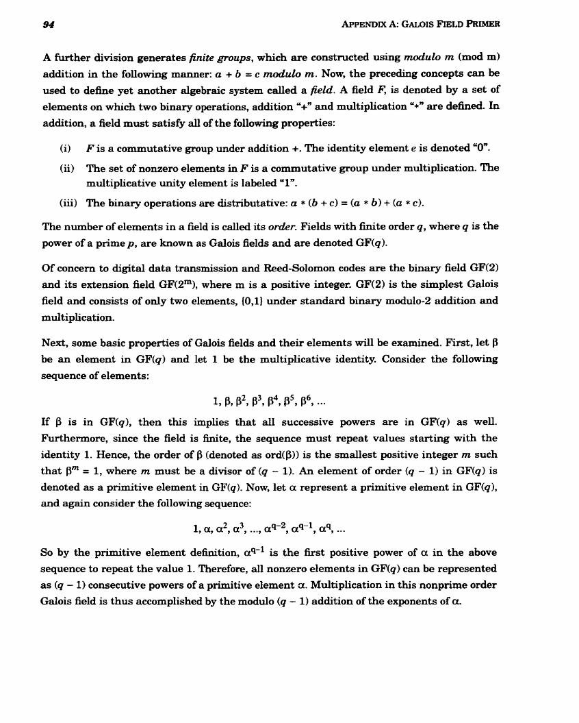
A further division generates finite groups, which are constmcted using modulo m (mod m)
addition in the following manner: a + b = c modulo m. Now, the preceding concepts can be
used to define yet another algebraic system called a field. A field F, is denoted by a set of
elements on which two binary operations, addition u+" and multiplication '*" are defined. In
addition, a field must satise al1 of the following properties:
(i) F is a commutative group under addition +. The identity element e is denoted "O*.
(ii) The set of nonzero elements in F is a commutative group under multiplication. The multiplicative unity element is labeled "1".
(iii) The binary operations are distributative: a * (b + c ) = (a * b ) + (a * c).
The number of elements in a field is called its order. Fields with finite order q, where q is the
power of a prime p, are known as Galois fields and are denoted GF(q).
Of concem to digital data transmission and Reed-Solomon codes are the binary field GF(2)
and its extension field GF(2m), where m is a positive integer. GF(2) is the simplest Galois
field and consists of only two elements, (0,l) under standard binary modulo-2 addition and
multiplication.
Next, some basic properties of Galois fields and their elements will be examined. First, let $
be an element in GF(q) and let 1 be the multiplicative identity. Consider the following
sequence of elements:
If f3 is in GF(q), then this implies that d successive powers are in GF(q) as well.
Furthermore, since the field is finite, the sequence must repeat values starting with the
identity 1. Hence, the order of P (denoted as ord(B)) is the smallest positive integer rn such
that firn = 1, where m must be a divisor of (q - 1). An element of order (q - 1) in GF(q) is
denoted as a primitive element in GF(q). Now, let a represent a primitive element in GF(q),
and again consider the following sequence:
So by the primitive element definition, aq-l is the fkst positive power of a in the above
sequence to repeat the value 1. Therefore, all nonzero elements in GF(q) can be represented
as (q - 1) consecutive powers of a primitive element a. Multiplication in this nonprime order
Galois field is thus accomplished by the modulo (q - 1) addition of the exponents of a.
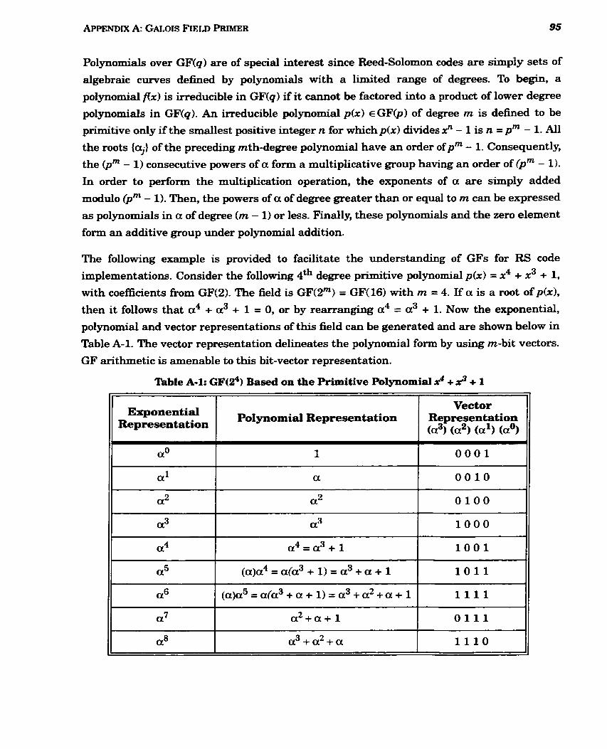
Polynomials over GF(q) are of special interest since Reed-Solomon codes are simply sets of
algebraic c w e s defined by polynomials with a limited range of degrees. To begin, a
polynomial m) is irreducible in GF(q) if it cannot be factored into a product of lower degree
polynomials in GF(q). An irreducible polynomial p(x) E GF@) of degree m is defined to be
primitive only if the smallest positive integer n for which p(x) divides x" - 1 is n = pm - 1. Al1
the mots (aj) of the preceding mth-degree polynomial have an order of pm - 1. Consequently,
the @" - 1) consecutive powers of a form a multiplicative group having an order of @* - 1) .
In order to perform the multiplication operation, the exponents of a are simply added
modulo (pm - 1). Then, the powers of a of degree greater than or equal to rn can be expressed
as plynomials in a of degree (rn - 1) or less. Finally, these polynomials and the zero element
form an additive group under polynomial addition.
The following example is provided to facilitate the understanding of GFs for RS code
implementations. Consider the following 4th degree primitive polynomial p(x) = x4 + x3 + 1,
with coefficients fkom GF(2). The field is GF(2m) = GF(16) with m = 4. If a is a root of p(x),
then it follows that a4 + a3 + 1 = O, or by remanging a4 = a3 + 1. Now the exponential,
polynomial and vector representations of this field can be generated and are shown below in
Table A-1. The vector representation delineates the polynomial form by using m-bit vectors.
GF arithmetic is amenable to this bit-vector representation.
Table A-1: OF(@) Based on the Primitive Polynomial x4 + 2 + 1
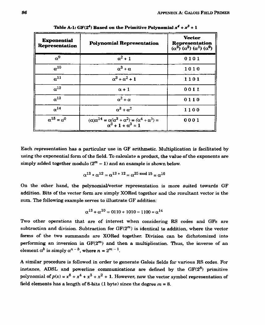
Table A-1: GF@) Based on the Primitive Polynomial x4 + 3 + 1
Each representation has a particular use in GE' arithmetic. Multiplication is facilitated by
using the exponential form of the field. To calculate a product, the value of the exponents are
simply added together modulo (2m - 1) and an example is shown below.
Exponential Representation
On the other hand, the polynomidvector representation is more suited towards GF
addition. Bits of the vector form are simply XORed together and the resultant vector is the
sum. The following example serves to illustrate GF addition:
' h o other operations that are of interest when considering RS codes and GFs are
subtraction and division. Subtraction for GF(2m) is identical to addition, where the vector
forms of the two summands are XORed together. Division can be dichotomized into
performing an inversion in GF(2m) and then a multiplication. Thus, the inverse of an
element ab is simply an - ', where n = 2m - l.
Polynomial Representation
A similar procedure is followed in order to generate Galois fields for various RS codes. For
instance, ADSL and powerline communications are defined by the ~ ~ ( 2 ~ 1 primitive
polynomial of p(x) = x8 + x4 + x3 + xZ + 1. However, now the vector symbol representation of
field elements has a length of 8-bits (1 byte) since the degree rn = 8.
Vector Representation (a3) (a2) (a1) (a0)
Appendix Ea Reed-Solomon MATLAB Code
B.1 Time-Domain Code
B.l.l Syndrome Calculation Oh TITLE: Syndrome Calculation % DESCRIPTION: Calculate Syndromes for an input received word YO This program does not use time sharing, it calculates YO 2t syndromes where t is defined below. Y0 % function synd = synCalc(r,n,t,tp) Y0 % Parameters Oh r: input received codeword as coefficients of xm-1, xAn-2, ..., x"O. % n: block length defined as (2%1)-1 % t: code's error correcting capability Oh tp: vector tuple containing al1 elements of GF(2Arn)
function synd = synCalc(r,n,t,tp)
O/O define alpha registers from ah1 to aA2't alpha = 1 :2Y;
% initialize registers to zero (alphaLlnf = zero) A(1:2*t) = -Inf; B(1:2*t) = -1nf;
O h Calculate 2t syndromes %for timestep = 1 :n, % for non-script purposes (simukte manually) for timestep = n:-1 :ln % have to reverse rx word input order [O .. . 141
for i = 1 :2*t,
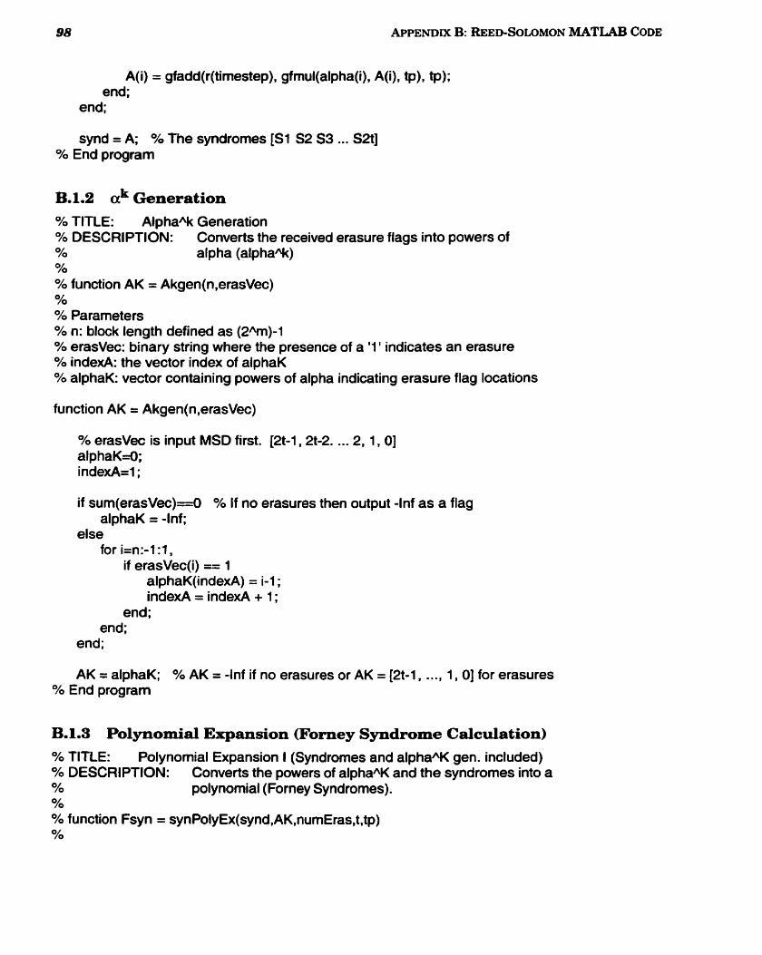
APPEND~X B: REED-SOLLIMON MATLAB CODE
A(i) = gfadd(r(timestep), gfmul(alpha(i), A(i), tp), tp); end;
end;
synd = A; % The syndromes [SI S2 S3 ... S2t] % End program
B.1.2 ak Generation % TITLE: Alpha* Generation % DESCRIPTION: Converts the received erasure flags into powers of % alpha (alpha*) Y0 % function AK = Akgen(n,erasVec) % % Parameters % n: block length defined as (2411)-1 % erasvec: binary string where the presence of a '1 ' indicates an erasure % index& the vector index of alphaK O h alphaK: vector containing powers of alpha indicating erasure flag locations
function AK = Akgen(n,erasVec)
% erasVec is input MSD first. [2t-1,2t-2. ... 2, 1, O] alphaK4; indexA=l ;
if sum(erasVec)==û % If no erasures then output -Inf as a flag alphaK = -Inf;
else for i=n:-1 :f ,
if erasVec(i) == 1 alphaK(indexA) = i-1 ; indexA = indexA + 1 ;
end; end;
end;
AK = alphaK; % AK = -1nf if no erasures or AK = [2t-1, ..., 1, O] for erasures % End program
B. 1.3 Polynomial Expansion (Forney Syndrome Calculation) % TITLE: Polynomial Expansion I (Syndromes and alphaAK gen. inctuded) % DESCRIPTION: Converts the powers of alphaAl( and the syndromes into a % polynomial (Forney Syndromes). =!A0
% function Fsyn = synPolyEx(synd,AK,nurnEras,t.tp) %
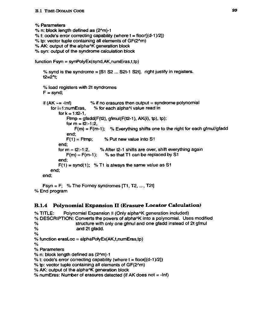
% Parameters % n: block length defined as (2%)-1 % t: code's error comting capability (where t = floor((d-1)/2]) Oh tp: vector tuple containing al1 elements of GF(2W) % AK: output of the alpha* generation block % syn: output of the syndrome calculation block
function Fsyn = synPolyEx(synd,AK,numEras,t,tp)
% synd is the syndrome = [SI S2 ... S2t-f S2t]. right justify in registers. t2=2*t;
% load registers with 2t syndromes F = synd;
if (AK -= -Inf) % if no erasures then output = syndrome polynomial for i=l :numEras, % for each alphaAi value read in
for k = 1 :t2-1, Ftmp = gfadd(F(t2), gfmul(F(t2-l ), AK(i), tp), tp); for m = t2:-1:2,
F(m) = F(m-1); Oh Everything shifts one to the right for each gfmul/gfadd end; F(l) = Ftmp; Oh Put new value into S1
end; for rn = t2:-1:2, % After t2-1 shifts are over, shift everything again
F(m) = F(m-1); % so that T l can be replaced by S1 end; F(1) = synd(1); % T l is always the sarne value as S I
end; end;
Fsyn = F; % The Forney syndromes [Tl, T2, ..., TZt] % End program
B.1.4 Polynomial Expansion II (Erasure Locator Cdculation)
% TITLE: Polynomial Expansion II (Only alphaAK generation included) Oh DESCRIPTION: Converts the powers of alpha")< into a polynomial. Uses modified YO structure with only one gfmul and one gfadd instead of 2t gfmul YO and 2t gfadd. Y0 Oh function erasLoc = alphaPolyEx(AK,t,numEras,tp) Y0 % Parameters % n: block length defined as (2%)-1 % t: code's error correcting capability (where t = floor[(d-l)/2]) % tp: vector tuple containing al1 elements of GF(2W) % AK: output of the alphaAK generation block % numEras: Number of erasures detected (if AK does not = -Inf)
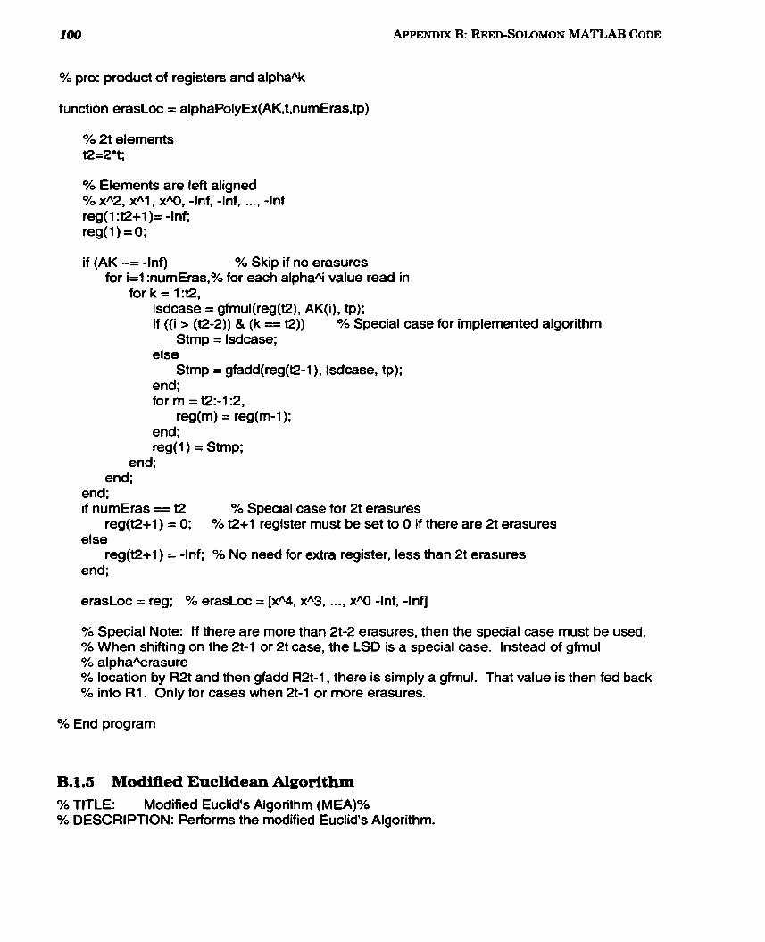
O/O pro: product of registers and alpha*
function erasLoc = alphaPolyEx(AK,t,numEras,tp)
% 2t elements t2=2*t;
% Elements are left aligned % xA2, xAl, x q , -Inf, -Inf, ..., -Inf reg(1 :t2+1)= -Inf; reg(1) = 0;
if (AK -= -Inf) % Skip if no erasures for i=l :numEras,% for each alphaq value read in
for k = 1 :t2, lsdcase = gfmul(reg(t2), AK(i), tp); if ((i > (t2-2)) & (k = t2)) O h Special case for implernented algorithm
Stmp = Isdcase; else
Stmp = gfadd(reg(t2-l ), Isdcase, tp); end; for m = t.2:-1:2,
reg(m) = reg(m-1); end; reg(1) = Stmp;
end; end;
end; if numEras -. t2 % Special case for 2t erasures
reg(t2+1) = 0; O h t2+1 register must be set to O if there are 2t erasures else
reg(t2+1) = -Inf; % No need for extra register, less than 2t erasures end;
erasLoc = reg; % erasLoc = [x*, xA3, ..., xW -inf, -Infl
% Special Note: If there are more than 2t-2 erasures, then the special case rnust be used. % When shifting on the 2t-1 or 2t case, the LSD is a special case. lnstead of gfmul O h alpha-rasure O h location by R2t and then gfadd R2t-1, there is simply a gfmul. That value is then fed back O h into R I . Only for cases when 2t-1 or more erasures.
% End prograrn
B.1.5 Modified Euclidean Algorithm % TITLE: Modified Euclid's Algorithm (MEA)% % DESCRI PTION: Perforrns the modified Euclid's Algorithm.

% % function eu = MEA(Fsyn,t,tp,numEras,erasLoc) % O/O Parameters Oh t: code's error correcting capability (where t = flwr[(d-l)/2]) % tp: vector tuple containing al1 elements of GF(2%) % numEras: Number of erasures detected (if AK does not = -Inf) % Fsyn: Forney syndrome corresponding to the received vector. Obtained from YO synPolyEx function. Oh erasloc: Erasure locator polynomial. Obtained from alphaPolyEx function.
function eu = MEA(Fsyn,t,tp,numEras,erasLoc)
% initializations maxShift=l; % extra space added to length of lambda and mu to accomodate shifting t2 = 2*t; sz = 2*t+l; % size of fields: 2t is max. degree, +1 for x'Y3 sr2 = 2't+l+maxShift; % mu could be sz long if t2 eras. could be shifted by
% maxShift if dR>>dQ doneFlag = 0;
% Power representation of field elements Q(1 ,sz) = -Inf; Q(1,1:12) = Fsyn;
mu(1 :sz2) = -Inf; for j=t2+1:-1:1,
if erasLoc(j) -= -Inf firstNonZ=j; break;
end; end; for j = 1 :firstNonZ,
rnu(j) = erasLoc(firstNonZ -j+l); end;
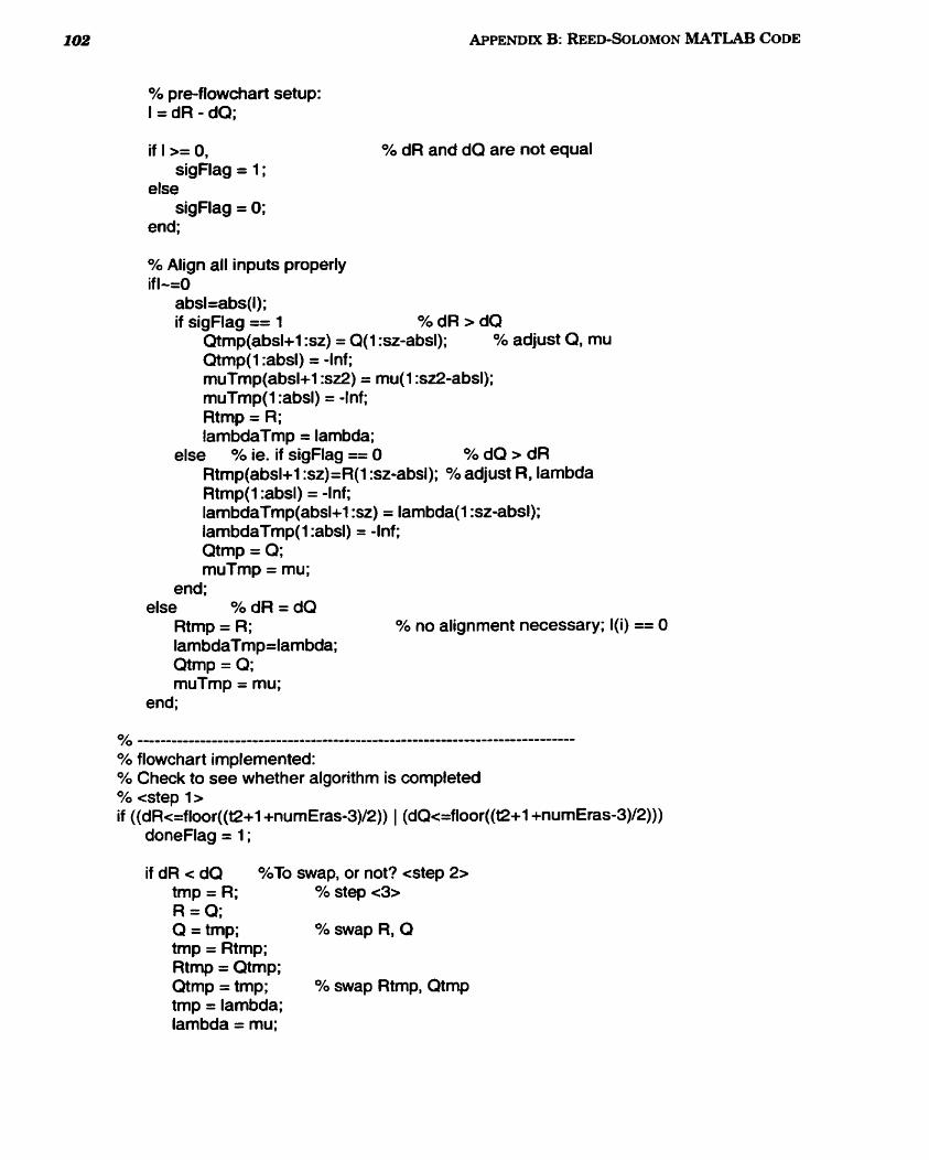
% pre-flowchart setup: I=dR-dQ;
if I >= 0, sigFlag = 1 ;
else sigFlag = 0;
end;
% dR and dQ are not equal
O h Align al1 inputs properly if l -=O
absl=abs(l); if sigFlag = 1 %dR>dQ
Qtmp(absl+l :sz) = Q(l :sz-absl); % adjust Q, mu Qtmp(1 :absl) = -Inf; muTmp(absl+l :sz2) = mu(1 :sa-absl); muTmp(1 :absl) = -1nf; Rtmp = R; IambdaTmp = lambda;
else % ie. if sigFlag == O %dQ>dR Rtmp(absl+l :sz)=R(1 :sr-absl); % adjust R, lambda Rtmp(1 :absl) = -Inf; lambdaTmp(absl+l :sz) = lambda(1 :sz-absl); lambdaTmp(1 :ab@ = -Inf; Qtmp = Q; muTmp = mu;
end; else %dR=dQ
Rtmp = R; % no alignment necessary; I(i) == O lambdaTmp=lambda; Qtmp = Q; muTmp = mu;
end;
% flowchart implemented: O h Check to see whether algorithm is completed '/O <step 1 > if ((dR<=floor((t2+1 +numEras-3)/2)) 1 (dQ<=floor((t2+1 +numEras-3)/2)))
doneFlag = 1 ;
if dR < dQ %To swap, or not? estep 2> tmp = R; % step <3> R = Q; Q = tmp; % swap R, Q tmp = Rtmp; Rtmp = Qtmp; Qtmp = tmp; O h swap Rtmp, Qtmp tmp = lambda; lambda = mu;
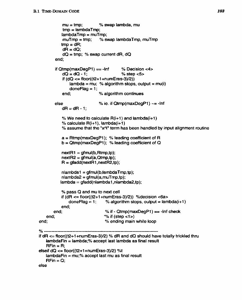
mu = tmp; % swap lambda, mu tmp = IambdaTmp; IambdaTmp = muimp; muTmp = tmp; % swap IambdaTmp, muTmp
tmp = dR; dR = dQ; dQ = tmp; % swap current dR, dQ
end;
if Qtmp(maxDegP1) = -Inf % Decision <4> dQ=dQ-1; % step <5> if (dQ c= floor((t2+1 +numEras-3)/2))
lambda = mu; O h algorithm stops, output = mu(i) doneFlag = 1 ;
end; % algorithm continues
else % ie. if Qtmp(maxDegP1) -= -Inf dR=dR-1;
% We need to calculate R(i+l ) and lambda(i+l) O h calculate R(i+l ), lambda(i+l ) O/O assume that the "xW term has been handled by input alignrnent routine
a = Rtmp(maxDegP1); % leading coefficient of R b = Qtmp(maxDegP1); % leading coefficient of Q
nlambdal = gfmul(b,lambdaTmp,tp); nlambda2 = gfmul(a,muTmp,tp); lambda = gfadd(nlambda1 ,nlambda2,tp);
O h pass Q and mu to next cefl if (dR <= floor((t2+1 +numEras-3)/2)) %decision <6a>
doneFlag = 1 ; O/O algorithm stops, output = larnbda(i+l ) end;
end; % if - Qtmp(maxDegP1) == -1nf check end; '% if (step < 1 >)
end; O h ending main white loop
........................................................................... if dR <= floor((t2+1 +numiEras-3)/2) % dR and dQ should have totally trkkled thru
lambdaFin = lambda;% accept last lambda as final result RFin = R;
elseif dQ <= floor((t2+1 +numEras-3)/2) Yot IambdaFin = mu;% accept last mu as final result RFin = Q;
else

'modEuc error - done all cells, but one of the degrees is still not < t' end; % if
tauleadingco = lambdaFin(1); AleadingCo = RFin(1);
if tauleadingco == -Inf 'modEuc error: IambdaFin is empty'
elseif AleadingCo = -Inf 'modEuc error: RFin is empty'
end;
eutmp(1,:) = lambdaFin(1 :sz); %tau = sigma errata lacator polynomial eutmp(2,:) = RFin; %A = omega errata evaluator polynomial eu = eutmp;
% End program
% TITLE: Chien search algorithm % DESCRIPTION: Performs the Chien search for finding the roots of the errata YO locator and evaluator polynomials o(x) and w(x) respectively. YO Does an exhaustive search and evaluates alphahi hi), o8(alpha&i) YO and w(alpha4) for O<= i <= n-1. % % function CS = Chien(eu,numEras,n,t,tp) % % Parameters O h euc: received errata locator and evaluator polynomials with coefficients of O h xw, x"1, ... xA2t-1. Oh n: block length defined as (2Am)-1 Oh t: code's error correcting capability (where t = floor[(d-1)/2]) % tp: vector tuple containing al1 efements of GF(2'hn) % deg: degree + 1 of input polynomial
function CS = Chien(eu,numEras,n,t,tp)
t2 = t'2; ohmflag = 0;
% Special case if maximum amount of erasures present if numEras -- t2
choice=t2 + 1; else
choice = t2; end;
O h define alpha registers from a q to aA2't becuase of case with 2t erasures alpha = 032;
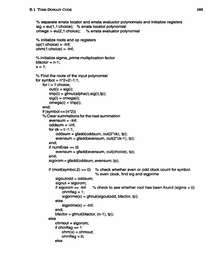
% separate errata locator and errata evaluator polynomials and initialize registers sig = eu(1,l :choice); % errata locator polynomial omega = eu(2,f :choice); % errata evaluator polynornial
% initialize roots and op registers op(1 :choice) = -Inf; ohm(1 :choice) = -Inf;
% initialize sigmajrime multiplication factor bfactor = n-1 ; x = 1;
% Find the roots of the input polynomial for symbol = ne2+2:-1 :1,
for i = 1 :choice, out(i) = sig(i); tmp(i) = gfmul(alpha(i),sig(i),tp) ; sig(i) = ornega(i); omega(i) = tmp(i);
end; if (symbol <= (n'2)) % Clear summations for the next summation
evensum = -Int oddsum = -Inf; for ck = t:-t :1,
oddsurn = gfadd(oddsum, out(2*ck), tp); evensum = gfadd(evensum, out(2'ck-l ), tp);
end; if numEras = t2
evensum = gfadd(evensum, out(choice), tp); end; sigorom = gfadd(oddsum, evensum, tp);
if (mod(symbol,2) == 0) % check whether even or odd dock count for symbol. O h even clock, find sig and sigprime
sigoutodd = oddsum; sigout = sigorom; if sigorom == -Inf % check to see whether root has been found (sigma = 0)
ohmflag = 1 ; sigprime(x) = gfmul(sigoutodd, bfactor, tp);
else sigprime(x) = -Inf;
end; bfactor = gfmul(bfactor, (n-1 ), tp);
else ohmout = sigorom; if ohrnflag = 1
ohrn(x) = ohmout; ohrnflag = 0;
else
ohm(x) = -Inf; end; x=x+1 ;
end; end;
end;
for i = n:-1 :l , if sigprime(i) -= -Inf
cser(n-i+l ) = gfdiv(ohm(i),sigprime(i),îp)'; else
cser(n-i+l ) = -Inf; end;
end;
CS = cser; % End program
B. 1.7 Polynomial Degree Determination % TITLE: Polynomial Degree Determination % DESCRIPTION: Determines the degree of the input polynomial
% Parameters % poly: Input polynornial % sr: length of the input polynomial vector
function degree = deg(poly,sz)
i = sz; degrf = 0; while i > 0,
if poly(i) -= -Inf degrf = i-1 ; i = l ;
end; i= i -1 ;
end; degree = degrf;
% End program
B.1.8 Sample Testbench % Tests only one error case with various erasure combinations.
% intialization of default parameters m = 8; % bits per message symboi p =2; % base of Galois field GF(p'9-n) n = 2Am-1 ; 5% codeword length

k = 239; % message length t = floor((n - k)/2); % error correction capability of RS code eflag = 0; 5% error flag initially O; x = 1; O/O error detector counter t2 = t*2;
tp = gftuple([-1 : pnm-2I1,m,p); % generate al1 elements in GF(2'Vn) Pg = rspoly(n, k,tp); % generator polynomial
NUM-ROW = 1 ; % Number of codewords that the program will correct MSG = randint(NUM-ROW,k, [-1 ,n-11, 1008); % 4 errors 8 erasures in this case
c = rsencode(MSG,Pg,n,tp); O h generation of RS codewords from message words erasV = randbit(1,255,(1 1 1 1 )/4, 901 ); % generation of 4 random errors erasVec = randbit(l,255,[1 1 1 1 1 1 1 ly8, 8); % generation of 8 random erasures
O h change -1 in c to -Inf for our algorithm for i=l :NUM-ROW,
for j=l :n, if c(i,j) = -1
c(i,j) = -1nf; elseif c(i,j) == n
c(i,j) =O; end;
end; end;
synd = synCalc(r,n,t,tp); numEras = sum(erasVec); AK = Akgen(n,erasVec); erasloc = alphaPolyEx(AK,t,numEras,tp); Fsyn = synPolyEx(synd,AK,numEras,t,tp); eu = M EA(Fsyn,t,tp,numEras,erasLoc); CS = Chien(eu,numEras,n,t,tp); rtmp = gfadd(cs,r,tp); isequal(rtmp,c)
% calculate the syndromes % finds the nurnber of erasures (if any) % finds the alpha powers from the erasure vector % calculate the errata locator polynomial % calculate the Forney syndromes % find omega and sigma polynomials Oh Chien search % add the corrected symbols with the input symbols % is the decoded codeword = generated codeword?
B.2 Frequency - Domain Code
B.2.l Syndrome Calculation % See Tirne-Domain Code (Section B.l.l) for Description function syn = synCalcBW(r,n,t,tp)
% load alpha registers for i = 1 :2't,
alpha(i)=i; end
% intialize registers to zero (alphah-lnf) A(f :2*t) = -Inf; B(1:2't) = -Inf;
%update each register for timestep = 1 :n,
for i = 1 :2't, A(i) = r(timestep); B(i) = gfadd(A(i), gfmul(alpha(i), B(i), tp), tp);
end; end
syn = B; % End Program
%alphaKgen: we're working in the power notation of GF elements % if the 1 st few elements of the input erasure flag sequence are 0, 1, 0, 1 ,.. % (ie. a '1' in positions that are erased) we should output alphaAl, aIphaA3,..
function aK = alphaKgen(n,erasVec)
if sum(erasVec)=O alphaK=O;
else for i=l :n
if erasVec(i) == 1 alphaK(indexA) = i-1 ; indexA = indexA + 1 ;
end %if end %for
end %if aK=alphaK;
% End Program
B.2.3 Erasure b a t o r Polynomial Calculation % See Tirne-Domain Code (Section B.1.4) for description function elp = alphaExp2(numEras,alph, t, tp)
%2t elements.
if numEras>O for i=l :nurnAtph % for each alphaAi value read in
pro=gfmul(alph(i), reg, tp); for j=l :t2 % for each register
reg(j)=gfadd(pro(j),reg(j+l ),tp); end reg(t2+1 )=pro(t2+f );
end end; elp = reg;
% End Program
Be2.4 Forney Syndrome Polynomial Calculation % See Time-Domain Code (Section 8.1.3) for explanation Y0 % numEras: number of erasures in codeword % syn: syndrome calculated from the syndrome unit % alph: powers of alpha correspondign to erasures % t: error correcting capability O/O tp: fist of al1 elements in GF(256), generated from tp = gftuple([-1 :ml]', m)
function Fsyn = polyExp2(numEras,syn, alph, t, tp)
%syn is the syndrome = SI S2 S3 S4 S5 S6. right justify in registers. t2=2*t; numAlph=length(alph); S=syn;
if numEras>O for i=l :numAlph % for each erasure (alpha+) input
prod=gfmul(alph(i), S(l :t2-l ), tp); for j=t2:-1:2 O h SI remains the sarne throughout caiculation
S(j)=gfadd(prod(j-1 ),S(j),tp); end
end end Fsyn=S;
% End Program
B.2.5 Modified Euclidean Algorithm % See Time-Domain Code (Section B.1.5) for Description Y0 % Fsyn: Forney syndrome corresponding to received vector % t: error correcting capability % tp: list of al1 elements in GF(256), generated from tp = gftuple([-1 :n-l]', m) O h numEras: number of erasures Oh erasloc: output of alphaExp: erasure locator polynomial
function sig = modEuc(Fsyn,t,tp,numEras,erasLoc)
% initializations maxShift=l ; % extra space added to length of lambda and mu to accomodate shifting i = l ; t2 = 2't; sz = 2'tcl; % size of fields: 2t is max. degree, +1 for xW sz2 = 2*t+l +maxShift; % mu could be sz long if t2 eras, could be shifted by
% maxShift if dR>>dQ
O h we are using the power representation of field elements Q = zeros(sz); Q(:,:) = -Inf; Q(1,l :t2) = Fsyn;
lambda = zeros(sz,sz2); lambda(:) = -Inf;
mu = zeros(sz,sz2); mu(:) = -Inf; for j=1 :t2+1
if eraslocfi) -= -Inf firstNonZ=j; break;
end; end; mu(l.1 :(t%firstNonZ+2)) = erasLoc(firstNonZ:t2+1);
%main cell loop (input to each cell is R, Q, start, lambda, and mu) for i = 1:t2,
maxDegPl = max(dR(i), dQ(i)) + 1 ;
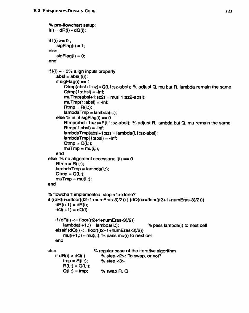
% pre-flowchart setup: l(i) = dR(i) - dQ(i);
if I(i) >= O , sigFlag(i) = 1 ;
else sigFlag(i) = 0;
end
if I(i) -= 0% align inputs properly absl = abs(l(i)); if sigFlag(i) == 1
Qtmp(absl+l :sz)=Q(i,l :sz-absl); % adjust Q, mu but R, lambda remain the same Qtmp(1 :absl) = 4nf; muTmp(absl+l :sz2) = mu(i, 1 :sz2-absl); muTmp(1 :absl) = -Inf; Rtmp = R(i,:); IambdaTmp = lambda(i, :);
else % ie. if sigFlag(i) == O Rtmp(absl+l :sz) =R(i, 1 :sz-absl); % adjust R, lambda but Q, mu remain the same Rtmp(1 :absl) = -Inf; lambdaTmp(absl+l :sz) = lambda& 1 :sz-absl); lambdaTmp(1 :absl) = -Inf; Qtmp = Q ( i , : ) ; muTmp = rnu(i,:);
end else Oh no alignment necessary; f(i) == O
Rtmp = R(i,:); IambdaTmp = lambda(i,:); Qtmp = Q(i,:); muTmp = mu(i,:);
end
% flowchart implernented: step c l >:done? if ((dR(i)<=floor((t2+1 +numErasS)/2)) 1 (dQ(i)<=floor((t2+1 +numEras-3)/2)))
dR(i+l ) = dR(i); dQ(i+l ) = dQ(i);
if (dR(i) <= floor((t2+1 +numEras-3)/2)) lambda(i+l ,:) = lambda(i,:); % pass lambda(i) to next cell
elseif (dQ(i) c= floor((t2+1 +numEras-3)/2)) mu(i+l ,:) = mu(i,:); % pass mu(i) to next cell
end
else % regular case of the iterative algorithm if dR(i) < dQ(i) % step Q>: To swap, or not?
tmp = R(i,:); O/O step <3> R(i,:) = Q(i,:); Q(i,:) = tmp; % swap R, Q
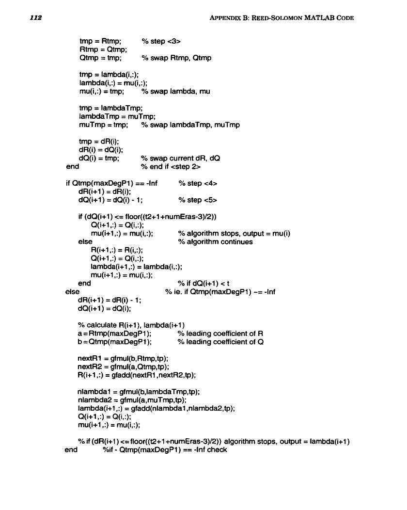
tmp = Rtmp; O h step <3> Rtmp = Qtmp; Qtmp = tmp; o/, swap Rtmp, Qtmp
trnp = lambda(i,:); lambda(i,:) = mu(i,:); mu(i,:) = tmp; % swap lambda, mu
trnp = IambdaTmp; IambdaTmp = muTmp; muTmp = trnp; % swap lambdafmp, muTmp
trnp = dR(i); dR(i) = dQ(i); dQ(i) = tmp; % swap current dR, dQ
end % end if cstep 2 w
if Qtmp(maxDegP1) == -Inf % step c4> dR(i+l ) = dR(i); dQ(i+l ) = dQ(i) - 1 ; % step c5>
if (dQ(i+l ) C= floor((t2+1 +numiiras-3)/2)) Q(i+1 ,:) = Q(i,:); mu(i+l ,:) = mu(i,:); % algorithm stops, output = mu(i)
else % algorithm continues R(i+l,:) = R(i,:); Q(i+l ,:) = Q(i,:); lambda(i+l ,:) = lambda(&:); mu(i+l ,:) = mu&:);
end % if dQ(i+l) c t else % ie. if Qtrnp(maxDegP1) -= -Inf
dR(i+l ) = dR(i) - 1 ; dQ(i+l ) = dQ(i);
Oh calculate R(i+l ), larnbda(i+l ) a = Rtmp(maxDegP1); % leading coefficient of R b = Qtmp(rnaxDegP1); O' leading coefficient of Q
nlambdal = gf mul(b,lambdaTmp,tp); nlambda2 = gfmul(a,muTmp,tp); lambda(i+l ,:) = gfadd(nlambda1 ,nlambda2,tp); Q(i+l , :) = Q(i,:); mu(i+l ,:) = mu(i,:);
% if (dR(i+l ) <= floor((t2+1 +numEras-3)/2)) algorithm stops, output = lambda(i+l ) end Ohif - Qtmp(maxDegP1) == -Inf check
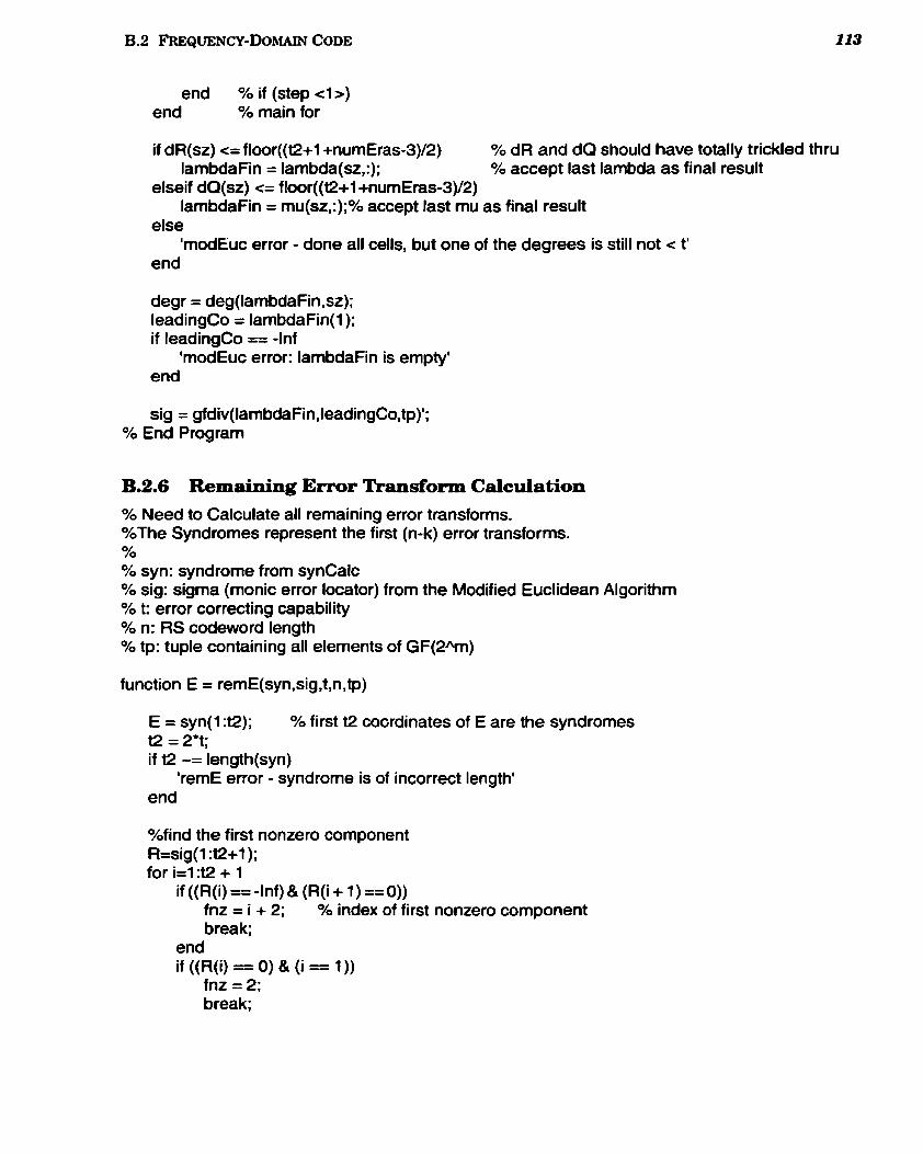
end % if (step e l w) end % main for
if dR(sz) <= floor((t2+1 +numEras-3)/2) % dR and dQ should have totally trickled thru IambdaFin = lambda(sz,:); % accept last lambda as final result
elseif dO(sz) <= f loor((t2+1 +numEras-3)/2) IambdaFin = rnu(sz,:);% accept last mu as final result
else 'modEuc error - done ail cells, but one of the degrees is still not < t'
end
degr = deg(1arnbdaFin.s~); IeadingCo = lambdaFin(1); if IeadingCo = -Inf
'modEuc error: IambdaFin is empty' end
sig = gfdiv(lambdaFin,leadingCo,tp)'; O h End Program
% Need to Calculate al1 remaining error transforms. OhThe Syndromes represent the first (n-k) error transforms. Y0 % syn: syndrome from synCalc % sig: sigma (monic error locator) from the Modified Euclidean Algorithm O h t: error correcting capability O h n: RS codeword length O h tp: tuple containing al1 elements of GF(24n)
function E = remE(syn,sig,t,n,tp)
E = syn(1 :t2); % first t2 co~rdinates of E are the syndromes t2 = 29; if t2 -= length(syn)
'remE error - syndrome is of incorrect length' end
%find the first nonzero component R=sig(l :t2+1); for i=1:t2 + 1
if ((R(i) == -1 nf) & (R(i + 1 ) == 0)) fnz = i + 2; Oh index of first nonzero component break;
end if ((R(i) == O) & (i = 1))
fnz = 2; break;
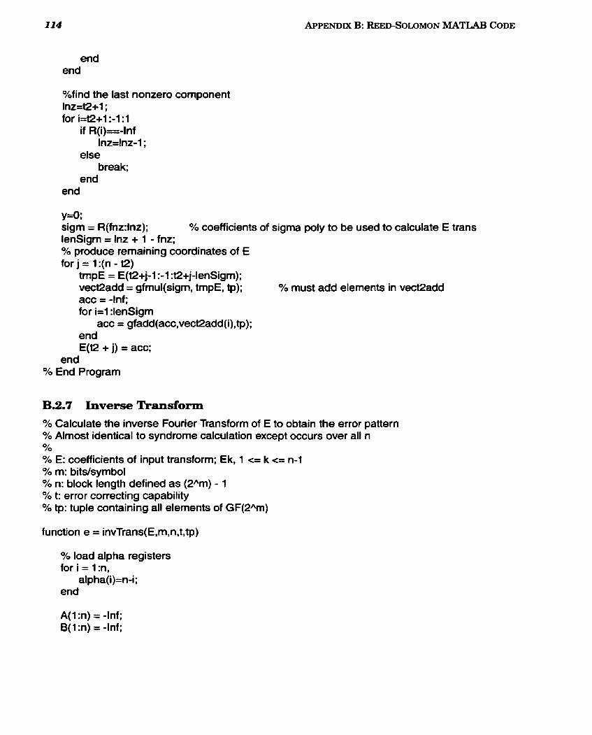
end end
Ohfind the last nonzero component Inz=t2+1; for i=t2+1:-1: 1
if R(i)=- l nf Inz=lnz-1 ;
else break;
end end
y=a sigm = R(fnz:lnz); % coefficients of sigma poly to be used to calculate E trans IenSigm = Inz + 1 - fnz; % produce remaining coordinates of E forj = l:(n - t2)
tmpE = E(t2+j-l :-l :t2+j-IenSigm); vect2add = gfmul(sigm, tmpE, tp); Oh must add elements in vect2add acc = -Inf; for i=l :lenSigm
acc = gfadd(acc1vect2add(i),tp); end E(t2 + j) = acc;
end O h End Program
Bm2,7 Inverse Transform % Calculate the inverse Fourier Transform of E to obtain the error pattern % Almost identical to syndrome calculation except occurs over al1 n Y0 % E: coefficients of input transform; Ek, 1 <= k <= n-1 % m: bits/symbol % n: block length defined as ( 2 h ) - 1 % t: error correcting capabitity % tp: tuple containing al1 elements of GF(2Am)
function e = invTrans(E,m,n,t,tp)
% load alpha registers for i = 1 :n,
alpha(i)=n-i; end
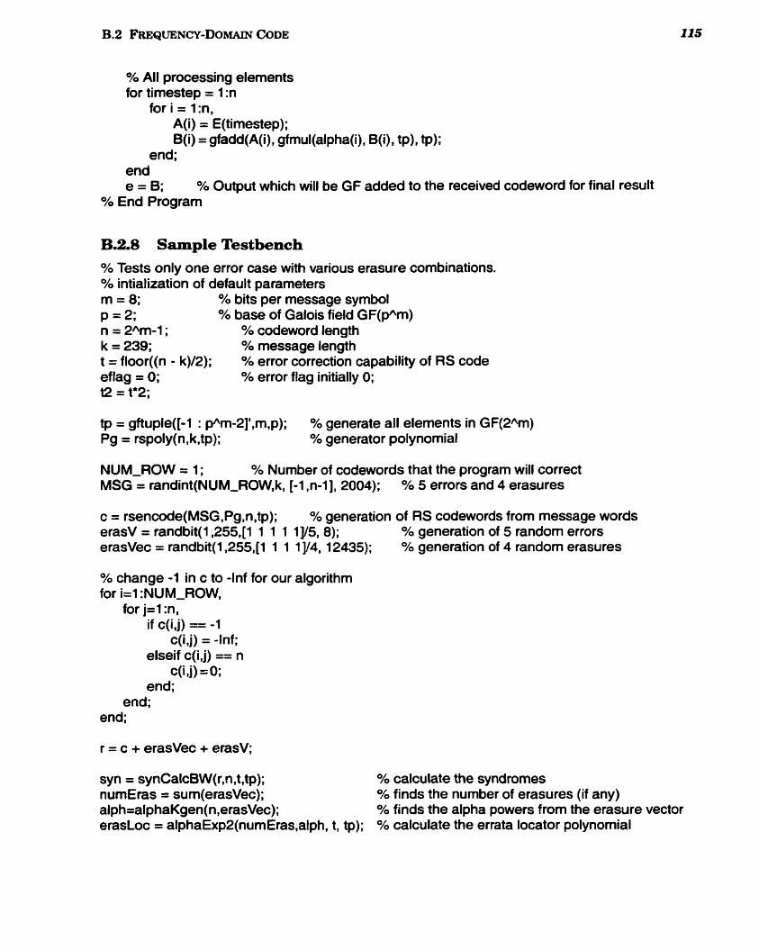
% All processing elements for timestep = 1 :n
for i = l:n, A(i) = E(timestep); B(i) = gfadd(A(i), gfmul(alpha(i), B(i), tp), tp);
end; end e = 6; % Output which will be GF added to the received codeword for final result
% End Program
B.2.8 Sample Testbench % Tests only one error case with various erasure combinations. % intialization of default parameters m = 8; % bits per message symbol p = 2; % base of Galois field GF(p"m) n = 2%-1; % codeword length k = 239; % message length t = floor((n - k)/2); % error correction capability of RS code eflag = 0; % error flag initially O; t2 = t'2;
tp = gftuple([-1 : Pm-2I8,rn,p); % generate al1 elements in GF(2hm) Pg = rspoly(n,k,tp); % generator polynomial
NUM-ROW = 1; % Number of codewords that the program will correct MSG = randint(NUM-ROW,k, [-1 ,n-11, 2004); % 5 errors and 4 erasures
c = rsencode(MSG ,Pg,n,tp); % generation of RS codewords from message words erasV = randbit(1,255,[1 1 1 1 1 YS, 8); % generation of 5 random errors erasvec = randbit(1,255,[1 1 1 1 y4, 12435); % generation of 4 random erasures
% change -1 in c to -1nf for our algorithm for i=l :NUM-ROW,
for j=l :n, if c(i,j) == -1
c(i,j) = -Inf; elseif c(i,j) == n
c(i,j) =O; end;
end; end;
syn = synCalcBW(r,n,t,tp); O h calculate the syndromes nurnEras = sum(erasVec); % finds the number of erasures (if any) alph=alphaKgen(n,erasVec); % finds the alpha powers from the erasure vector erasLoc = alphaExp2(numEras,alph, t, tp); O h calculate the errata locator polynomial
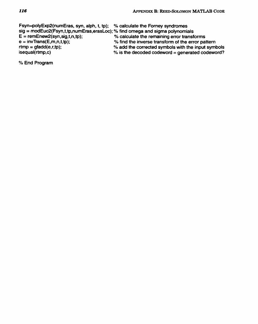
Fsyn=polyExp2(numEras, syn, alph, t, tp); % calculate the Fomey syndromes sig = modEuc2(Fsyn,t,tp.numEras,erasLoc); % find ornega and sigma polynomials E = remEnew2(syn,sig,t,n,tp); % calculate the remaining error transforms e = invTrans(E,m,n,t,tp); % find the inverse transform of the error pattern rtmp = gfadd(e, r,tp); % add the corrected symbols with the input symbols isequal(rtmp,c) % is the decoded codeword = generated codeword?
% End Prograrn

Appendix
Software Profiling Results
C.l Tirne-Domain Profiking Session
The following profiling session was obtained using the gprof program. First, some of the
more relevant process names found in Table C-2 and Table C-3 are explained as follows:
'Iàble C-1: Profiler Rocess Name Explanations 1
Process Name
II syndrome
Explanation 1 Evaluate the errata polynomials by performing the
Chien search algorithm. II AU multiplication functions. 1 I
Initialize interna1 CPU memory for the given program. II Syndrome calculation unit.
Modified Euclidean algorithm. - - --
Initialize all polynomials and variables for the modified Euclidean decoding algorithm. II
Overall decoder program which calls the above functions.
FDD inverse transform calculation unit.
FDD remaining error transform calculation unit.
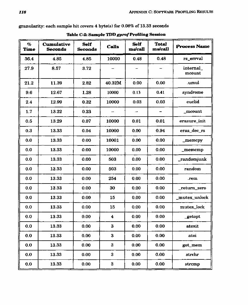
granularity: each sample hit covers 4 byte(s) for 0.08% of 13.33 seconds
Rofess Name
rserrval
intemal- mcount
.umd
syndrome
euclid
- mcount
erasure-init
eras-dec-rs
-memcpy
- memcmp
- randomjunk
random
.rem - --
- return-zero
- mutex-dock
mutex-lock
xetopt
atexit
atoi
get-mem
strchr
s trcmp
% Tirne
36.4
, 27.9
21.2
9.6
2.4
1.7
0.5
0.3
0.0
0.0
0.0
0.0
0.0
0.0
0.0
0.0
0.0
0.0
0.0
0.0
0.0
0.0
TIlD gpmf
10000
-
40.32M
1OOOO
10000
-
10000
10000
10001
10000
503
503
254
30
15
15
4
3
3
3
3
3
Table
Cumulative Seconds
4.85
8.57
11.39
12.67
12.99
13.22
13.29
13.33
13.33
13.33
13.33
13.33
13.33
13.33
13.33
13.33
13.33
13.33
13.33
13.33
13.33
13.33
Profiling
Self malcd
0.48
-
0.00
0.13
0.03
-
0.01
0.00
0.00
0.00
0.00
0.00
0.00
0.00
0.00
0.00
0.00
0.00
0.00
0.00
0.00
0.00
(3-2: Sample
' Self Seconds
4.85
3.72
2.82
1.28
0.32
0.23
0.07
0.04
0.00
0.00
0.00
0.00
0.00
0.00
0.00
0.00
0.00
0.00
0.00
0.00
0.00
0.00
Session
mslcd
0.48
-
0.00
0.4 1
0.03
-
0.01
0.94
0.00
0.00
0.00
0.00
0.00
0.00
0.00
0.00
0.00
0.00
0.00
0.00
0.00
0.00
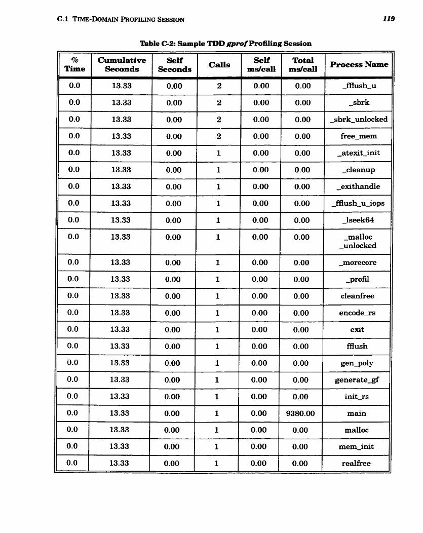
% Time
0.0
0.0
0.0
0.0
0.0
0.0
0.0
0.0
0.0
0.0
0.0
0.0
0.0
0.0
0.0
0.0
0.0
0.0
0.0
0.0
0.0
0.0
0.0
'iàble
Cumulative Seconds
13.33
13.33
13.33
13.33
13.33
13.33
13.33
13.33
13.33
13.33
13.33
13.33
13.33
13.33
13.33
13.33
13.33
13.33
13.33
13.33
13.33
13.33
13.33
C-2= Sample
Self Seconds
0.00
0.00
0.00
0.00
0.00
0.00
0.00
0.00
0.00
0.00
0.00
0.00
0.00
0.00
0.00
0.00
0.00
0.00
0.00
O. O0
0.00
0.00
0.00
Profiling
Self ms /cd
0.00
0.00
0.00
0.00
0.00
0.00
0.00
0.00
0.00
0.00
0.00
0.00
0.00
0.00
0.00
0.00
0.00
0.00
0.00
0.00
0.00
0.00
0.00
TDD gpmf
Caus
2
2
2
2
1
1
1
1
1
1
1
1
1
1
1
1
1
1
1
1
1
1
1
Session
rns/cd
0.00
0.00
0.00
0.00
0.00
0.00
0.00
0.00
0.00
0.00
0.00
0.00
0.00
0.00
0.00
0.00
0.00
0.00
0.00
9380.00
0.00
0.00
0.00
Process Name
- fflush-u
- sbrk
- sbrk-unlocked
free-mem
- atexitinit
- cleanup
- exithandle
- fflush-u-iops
- lseek64
malloc - hocked
- morecore
- profil
cleanhe
encoders
exit
fflush
gen-poly
generates
init-rs
main
mdloc
meminit
realfi.ee
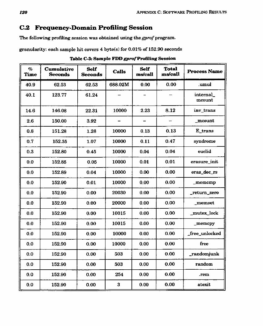
C.2 Frequency-Domain Profiling Session
The following profiling session was obtained using the gprof program.
grandarity: each sample hit covers 4 byteCs) for 0.01% of 152.90 seconds
ab le C-3: Sample FDD gpmf Proiiiing Session
..
h c e s s ~ a m e
.umd
intemal- mcount
inv-tram
- mcount
E-tram
syndrome
euclid
erasure-init
eras-dec-rs
- memcmp
- ret-zero
- memset
- mutex-lock
- memcpy
- fkee-unlocked
free
- randornjunk
random
.rem
atexit
% Time
40.9
40.1
14.6
2.6
0.8
0.7
0.3
0.0
0.0
0.0
0.0
0.0
0.0
0.0
0.0
0.0
0.0
0.0
0.0
0.0
688.02M
-
10000
-
10000
10000
10000
10000
10000
10000
20030
20000
10015
10015
10000
10000
503
503
254
3
Cumulative Seconds
62.53
123.77
146.08
150.00
151.28
152.35
152.80
152.85
152.89
152.90
152.90
152.90
152.90
152.90
152.90
152.90
152.90
152.90
152.90
152.90 l
Self ms/calï
0.00
-
2.23
-
O. 13
O. 11
0.04
0.01
0.00
0.00
0.00
0.00
0.00
0.00
0.00
0.00
0.00
0.00
0.00
0.00
Self Seconds
62.53
61.24
22.31
3.92
1.28
1.07
0.45
0.05
0.04
0.01
0.00
0.00
0.00
0.00
0.00
O. O0
0.00
0.00
0.00
0.00
ms/call
0.00
-
8.12
-
O. 13
0.47
0.04
0.01
0.00
0.00
0.00
0.00
0.00
0.00
0.00
0.00
0.00
0.00
0.00
0.00
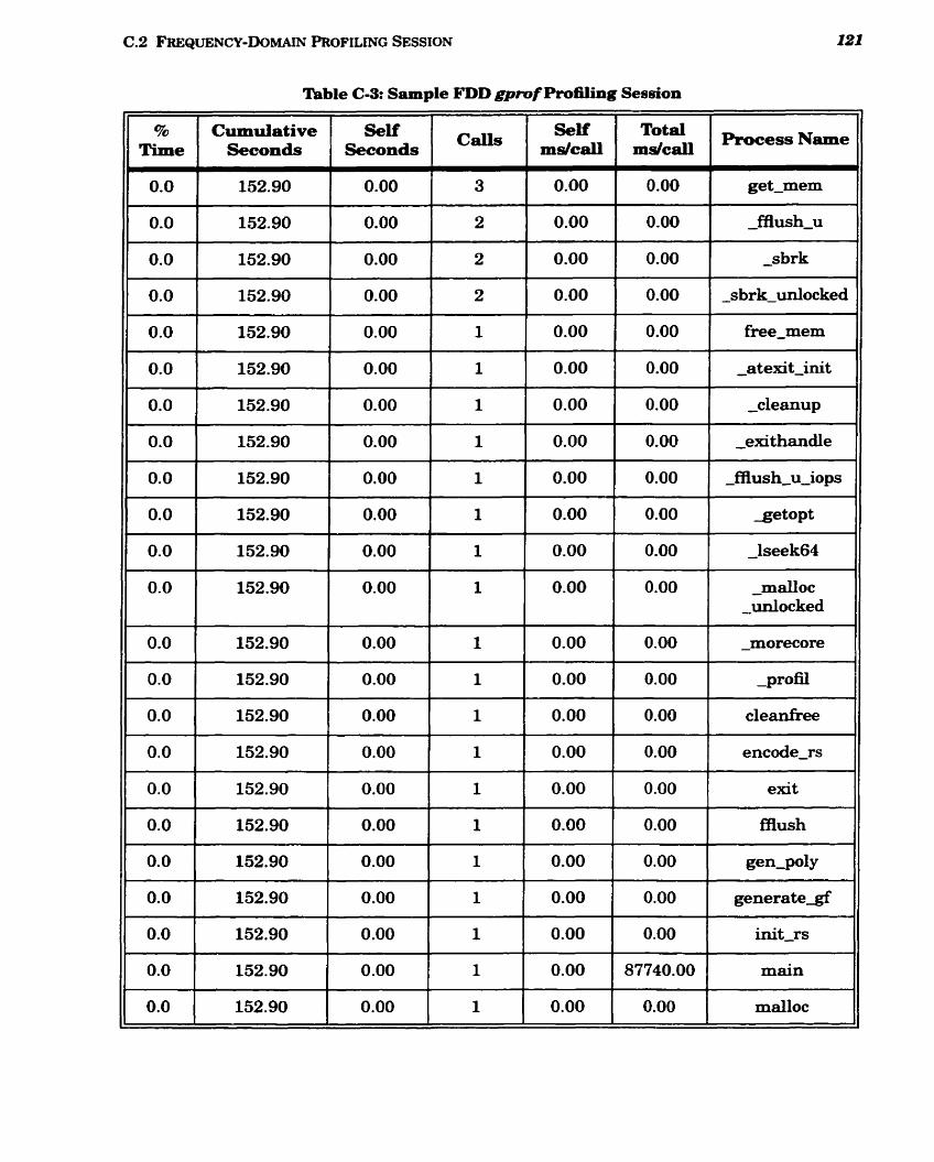
Session
m s / d
0.00
0.00
0.00
0.00
0.00
0.00
0.00
0.00
0.00
0.00
0.00
0.00
0.00
0.00
0.00
0.00
0.00
0.00
0.00
0.00
0.00
87740.00
0.00
FDD gpmf
3
2
2
2
1
1
1
1
1
1
1
1
1
1
1
1
1
1
1
1
1
1
1
Process N-= I
get-mem
- fflush-u
- sbrk
- sbrk-unlocked
free-mem
- atexit-init
- cleanup
- exit handle
- fflushuiops
zetopt
- lseek64
malloc - Locked
morecore -
- profil
cle8Ilfree
encoders
exit
fflush
g e n - ~ l ~
generated
init-rs
main
malloc
C-3: Sample
Self Seconds
0.00
0.00
0.00
0.00
0.00
0.00
0.00
0.00
0.00
0.00
0.00
0.00
0.00
0.00
0.00
0.00
0.00
0.00
0.00
0.00
0.00
0.00
0.00
% Time
0.0
0.0
0.0
0.0
0.0
0.0
0.0
0.0
0.0
0.0
0.0
0.0
0.0
0.0
0.0
0.0
0.0
0.0
O. O
0.0
0.0
0.0
0.0
Proiiling
Self rns/ca
0.00
0.00
0.00
0.00
0.00
0.00
0.00
0.00
0.00
0.00
0.00
0.00
0.00
0.00
0.00
0.00
0.00
0.00
0.00
0.00
0.00
0.00
0.00
a b l e
Cumulative Seconds
152.90
152.90
152.90
152.90
152.90
152.90
152.90
152.90
152.90
152.90
152.90
152.90
152.90
152.90
152.90
152.90
152.90
152.90
152.90
152.90
152.90
152.90
152.90
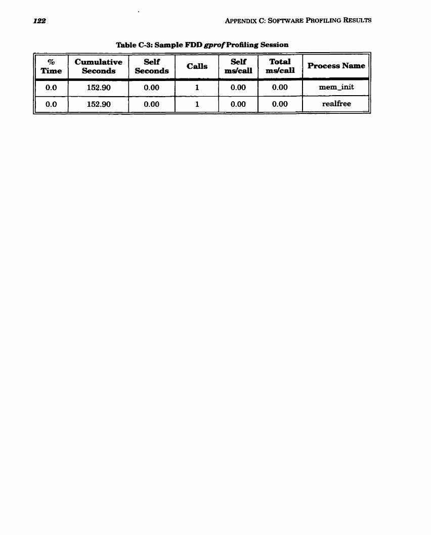
APPENDIX C: SOFTWARE PROFILING RESULTS
a b l e C-3: Sarnple FDD gpmf Profiiing Session
70 Time
0.0
0.0
Cumulative Seconds
152.90
152.90
Self Seconds
0.00
0.00
1
1
Seif msicall
0.00
0.00
msicaU
0.00
0.00
PmeesgName
mem-init
reabee