Embed Size (px)
Citation preview
Octal LNA/VGA/AAF/ADC and Crosspoint Switch
AD9271
Rev. B Information furnished by Analog Devices is believed to be accurate and reliable. However, no responsibility is assumed by Analog Devices for its use, nor for any infringements of patents or other rights of third parties that may result from its use. Specifications subject to change without notice. No license is granted by implication or otherwise under any patent or patent rights of Analog Devices. Trademarks and registered trademarks are the property of their respective owners.
One Technology Way, P.O. Box 9106, Norwood, MA 02062-9106, U.S.A.Tel: 781.329.4700 www.analog.com Fax: 781.461.3113 ©2007–2009 Analog Devices, Inc. All rights reserved.
FEATURES 8 channels of LNA, VGA, AAF, and ADC Low noise preamplifier (LNA)
Input-referred noise = 1.1 nV/√Hz @ 5 MHz typical, gain = 18 dB
SPI-programmable gain = 14 dB/15.6 dB/18 dB Single-ended input; VIN maximum = 400 mV p-p/
333 mV p-p/250 mV p-p Dual-mode active input impedance matching Bandwidth (BW) > 70 MHz Full-scale (FS) output = 2 V p-p differential
Variable gain amplifier (VGA) Gain range = −6 dB to +24 dB Linear-in-dB gain control
Antialiasing filter (AAF) 3rd-order Butterworth cutoff Programmable from 8 MHz to 18 MHz
Analog-to-digital converter (ADC) 12 bits at 10 MSPS to 50 MSPS SNR = 70 dB SFDR = 80 dB Serial LVDS (ANSI-644, IEEE 1596.3 reduced range link) Data and frame clock outputs
Includes crosspoint switch to support continuous wave (CW) Doppler
Low power, 150 mW per channel at 12 bits/40 MSPS (TGC) 90 mW per channel in CW Doppler Single 1.8 V supply (3.3 V supply for CW Doppler output bias) Flexible power-down modes Overload recovery in <10 ns Fast recovery from low power standby mode, <2 μs 100-lead TQFP
APPLICATIONS Medical imaging/ultrasound Automotive radar
GENERAL DESCRIPTION The AD9271 is designed for low cost, low power, small size, and ease of use. It contains eight channels of a variable gain amp-lifier (VGA) with low noise preamplifier (LNA); an antialiasing filter (AAF); and a 12-bit, 10 MSPS to 50 MSPS analog-to-digital converter (ADC).
Each channel features a variable gain range of 30 dB, a fully differential signal path, an active input preamplifier termination, a maximum gain of up to 40 dB, and an ADC with a conversion rate of up to 50 MSPS. The channel is optimized for dynamic performance and low power in applications where a small package size is critical.
FUNCTIONAL BLOCK DIAGRAM
SER
IAL
POR
TIN
TER
FAC
E
REFERENCE
FCO+FCO–DCO+DCO–
LNA
LO-HLOSW-H
LI-HLG-H
12-BITADC
SERIALLVDS
DOUTH+DOUTH–
LNA
LO-GLOSW-G
LI-GLG-G
12-BITADC
SERIALLVDS
DOUTG+DOUTG–
LNA
LO-FLOSW-F
LI-FLG-F
12-BITADC
SERIALLVDS
DOUTF+DOUTF–
LNA
LO-ELOSW-E
LI-ELG-E
12-BITADC
SERIALLVDS
DOUTE+DOUTE–
LNA
LO-DLOSW-D
LI-DLG-D
12-BITADC
SERIALLVDS
DOUTD+DOUTD–
LNA
LO-CLOSW-C
LI-CLG-C
12-BITADC
SERIALLVDS
DOUTC+DOUTC–
LNA
LO-BLOSW-B
LI-BLG-B
LNA
LO-ALOSW-A
LI-ALG-A
12-BITADC
SERIALLVDS
DOUTB+DOUTB–
12-BITADC
SERIALLVDS
DOUTA+DOUTA–
AVD
D
STB
Y
DR
VDD
PDW
N
CLK
–C
LK+
SDIO
SCLK
CSB
RB
IAS
REF
TR
EFB
VREF
SEN
SE
GA
IN+
GA
IN–
CW
D[5
:0]+
/–C
WVD
D
SWITCHARRAY
DA
TAR
ATE
MU
LTIP
LIER
0630
4-00
1
AAF
AAF
AAF
AAF
AAF
AAF
AAF
AAF
AD9271
VGA
VGA
VGA
VGA
VGA
VGA
VGA
VGA
Figure 1.
The LNA has a single-ended-to-differential gain that is selectable through the SPI. The LNA input noise is typically 1.2 nV/√Hz, and the combined input-referred noise of the entire channel is 1.4 nV/√Hz at maximum gain. Assuming a 15 MHz noise bandwidth (NBW) and a 15.6 dB LNA gain, the input SNR is roughly 86 dB. In CW Doppler mode, the LNA output drives a transconductance amp that is switched through an 8 × 6 differential crosspoint switch. The switch is programmable through the SPI.
AD9271
Rev. B | Page 2 of 60
TABLE OF CONTENTS Features .............................................................................................. 1 Applications ....................................................................................... 1 General Description ......................................................................... 1 Functional Block Diagram .............................................................. 1 Revision History ............................................................................... 2 Product Highlights ........................................................................... 3 Specifications ..................................................................................... 4
AC Specifications .......................................................................... 4 Digital Specifications ................................................................... 7 Switching Specifications .............................................................. 8 ADC Timing Diagrams ............................................................... 9
Absolute Maximum Ratings .......................................................... 10 Thermal Impedance ................................................................... 10 ESD Caution ................................................................................ 10
Pin Configuration and Function Descriptions ........................... 11 Equivalent Circuits ......................................................................... 14 Typical Performance Characteristics ........................................... 16 Theory of Operation ...................................................................... 20
Ultrasound ................................................................................... 20 Channel Overview ...................................................................... 21 Input Overdrive .......................................................................... 23 CW Doppler Operation ............................................................. 24
TGC Operation ........................................................................... 25 ADC ............................................................................................. 27 Clock Input Considerations ...................................................... 28
Serial Port Interface (SPI) .............................................................. 35 Hardware Interface ..................................................................... 35
Memory Map .................................................................................. 37 Reading the Memory Map Table .............................................. 37 Reserved Locations .................................................................... 37 Default Values ............................................................................. 37 Logic Levels ................................................................................. 37
Applications Information .............................................................. 41 Design Guidelines ...................................................................... 41
Evaluation Board ............................................................................ 42 Power Supplies ............................................................................ 42 Input Signals................................................................................ 42 Output Signals ............................................................................ 42 Default Operation and Jumper Selection Settings ................. 43 Quick Start Procedure ............................................................... 44 Schematics and Artwork ........................................................... 45
Outline Dimensions ....................................................................... 58 Ordering Guide .......................................................................... 58
REVISION HISTORY 5/09—Rev. A to Rev. B
Changes to Figure 27 ...................................................................... 17 Changes to Figure 40 and Figure 41 ............................................. 21 Changes to Ordering Guide .......................................................... 58
12/07—Rev. 0 to Rev. A
Change to AC Specifications Text .................................................. 4 Added Input Noise Current ............................................................ 4 Added Noise Figure .......................................................................... 4 Changes to Signal-to-Noise Ratio Units ........................................ 4 Changes to Harmonic Distortion Units ........................................ 5 Added Endnote 3 .............................................................................. 6 Changes to Table 6 .......................................................................... 11 Inserted Figure 19 and Figure 21 .................................................. 16 Changes to Figure 20 ...................................................................... 16 Changes to Theory of Operation Section .................................... 20 Changes to Figure 40 and Figure 41 ............................................. 21 Change to Active Impedance Matching Section ........................ 22
Changes to LNA Noise Section .................................................... 22 Changes to Figure 43 ...................................................................... 22 Change to Input Overload Protection Section ........................... 23 Changes to TGC Operation Section ............................................ 25 Changes to Gain Control Section ................................................. 26 Changes to Figure 52 ...................................................................... 26 Change to Table 11 ......................................................................... 33 Changes to Serial Interface Port (SPI) Section ........................... 35 Changes to Hardware Interface Section ...................................... 35 Changes to Reading the Memory Map Table Section ............... 37 Added Applications Information and Design Guidelines Sections ...................................................... 41 Change to Input Signals Section ................................................... 42 Changes to Figure 73 ...................................................................... 42 Changes to Table 16 ....................................................................... 55
6/07—Revision 0: Initial Version
AD9271
Rev. B | Page 3 of 60
The AD9271 requires a LVPECL-/CMOS-/LVDS-compatible sample rate clock for full performance operation. No external reference or driver components are required for many applications.
The ADC automatically multiplies the sample rate clock for the appropriate LVDS serial data rate. A data clock (DCO±) for capturing data on the output and a frame clock (FCO±) trigger for signaling a new output byte are provided.
Powering down individual channels is supported to increase battery life for portable applications. There is also a standby mode option that allows quick power-up for power cycling. In CW Doppler operation, the VGA, AAF, and ADC are powered down. The power of the TGC path scales with selectable speed grades.
The ADC contains several features designed to maximize flexibility and minimize system cost, such as a programmable clock, data alignment, and programmable digital test pattern generation. The digital test patterns include built-in fixed patterns, built-in pseudorandom patterns, and custom user-defined test patterns entered via the serial port interface.
Fabricated in an advanced CMOS process, the AD9271 is available in a 16 mm × 16 mm, RoHS compliant, 100-lead TQFP. It is specified over the industrial temperature range of −40°C to +85°C.
PRODUCT HIGHLIGHTS 1. Small Footprint. Eight channels are contained in a small,
space-saving package. Full TGC path, ADC, and crosspoint switch contained within a 100-lead, 16 mm × 16 mm TQFP.
2. Low Power of 150 mW per Channel at 40 MSPS. 3. Integrated Crosspoint Switch. This switch allows numerous
multichannel configuration options to enable the CW Doppler mode.
4. Ease of Use. A data clock output (DCO±) operates up to 300 MHz and supports double data rate (DDR) operation.
5. User Flexibility. Serial port interface (SPI) control offers a wide range of flexible features to meet specific system requirements.
6. Integrated Third-Order Antialiasing Filter. This filter is placed between the TGC path and the ADC and is programmable from 8 MHz to 18 MHz.
AD9271
Rev. B | Page 4 of 60
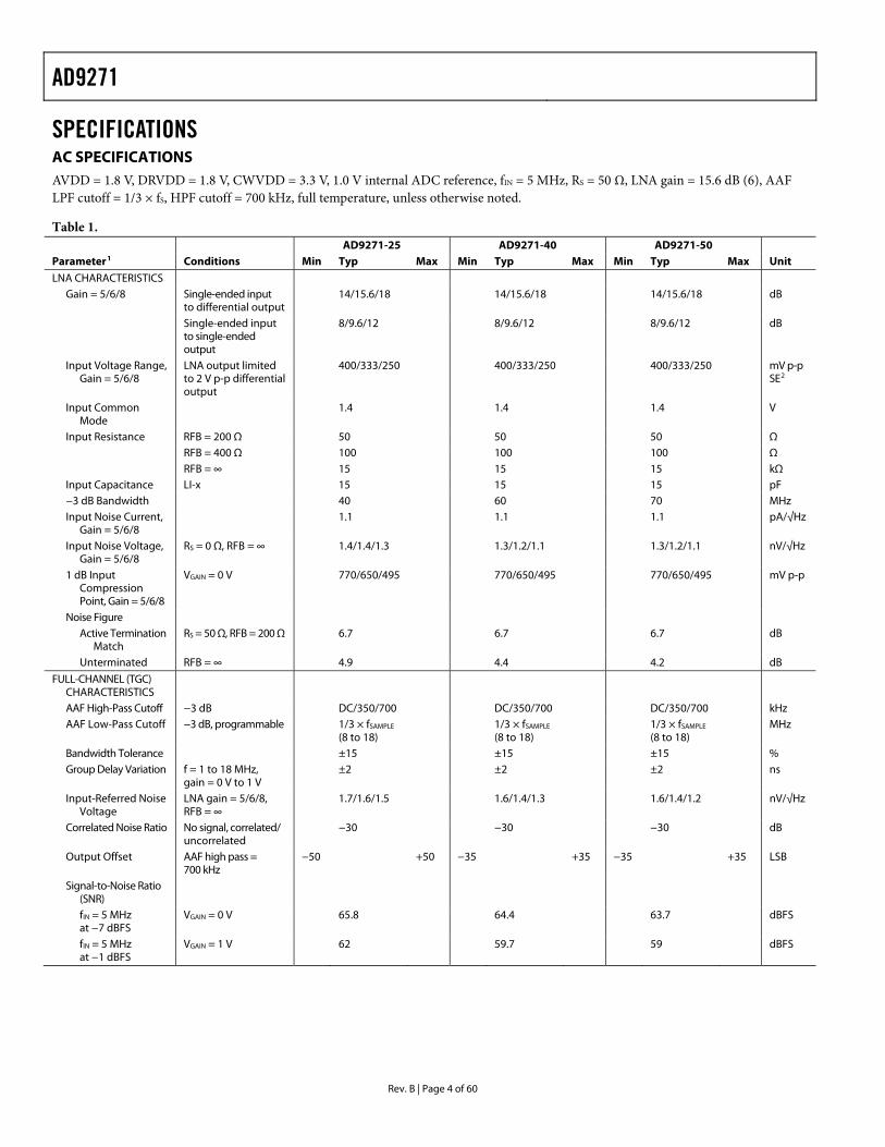
SPECIFICATIONS AC SPECIFICATIONS AVDD = 1.8 V, DRVDD = 1.8 V, CWVDD = 3.3 V, 1.0 V internal ADC reference, fIN = 5 MHz, RS = 50 Ω, LNA gain = 15.6 dB (6), AAF LPF cutoff = 1/3 × fS, HPF cutoff = 700 kHz, full temperature, unless otherwise noted.
Table 1. AD9271-25 AD9271-40 AD9271-50 Parameter1 Conditions Min Typ Max Min Typ Max Min Typ Max Unit
LNA CHARACTERISTICS Gain = 5/6/8 Single-ended input
to differential output 14/15.6/18 14/15.6/18 14/15.6/18 dB
Single-ended input to single-ended output
8/9.6/12 8/9.6/12 8/9.6/12 dB
Input Voltage Range, Gain = 5/6/8
LNA output limited to 2 V p-p differential output
400/333/250 400/333/250 400/333/250 mV p-p SE2
Input Common Mode
1.4 1.4 1.4 V
Input Resistance RFB = 200 Ω 50 50 50 Ω RFB = 400 Ω 100 100 100 Ω RFB = ∞ 15 15 15 kΩ Input Capacitance LI-x 15 15 15 pF −3 dB Bandwidth 40 60 70 MHz Input Noise Current,
Gain = 5/6/8 1.1 1.1 1.1 pA/√Hz
Input Noise Voltage, Gain = 5/6/8
RS = 0 Ω, RFB = ∞ 1.4/1.4/1.3 1.3/1.2/1.1 1.3/1.2/1.1 nV/√Hz
1 dB Input Compression Point, Gain = 5/6/8
VGAIN = 0 V 770/650/495 770/650/495 770/650/495 mV p-p
Noise Figure Active Termination
Match RS = 50 Ω, RFB = 200 Ω 6.7 6.7 6.7 dB
Unterminated RFB = ∞ 4.9 4.4 4.2 dB
FULL-CHANNEL (TGC) CHARACTERISTICS
AAF High-Pass Cutoff −3 dB DC/350/700 DC/350/700 DC/350/700 kHz AAF Low-Pass Cutoff −3 dB, programmable 1/3 × fSAMPLE
(8 to 18) 1/3 × fSAMPLE
(8 to 18) 1/3 × fSAMPLE
(8 to 18) MHz
Bandwidth Tolerance ±15 ±15 ±15 % Group Delay Variation f = 1 to 18 MHz,
gain = 0 V to 1 V ±2 ±2 ±2 ns
Input-Referred Noise Voltage
LNA gain = 5/6/8, RFB = ∞
1.7/1.6/1.5 1.6/1.4/1.3 1.6/1.4/1.2 nV/√Hz
Correlated Noise Ratio No signal, correlated/ uncorrelated
−30 −30 −30 dB
Output Offset AAF high pass = 700 kHz
−50 +50 −35 +35 −35 +35 LSB
Signal-to-Noise Ratio (SNR)
fIN = 5 MHz at −7 dBFS
VGAIN = 0 V 65.8 64.4 63.7 dBFS
fIN = 5 MHz at −1 dBFS
VGAIN = 1 V 62 59.7 59 dBFS
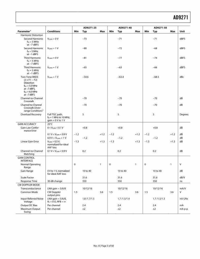
AD9271
Rev. B | Page 5 of 60
AD9271-25 AD9271-40 AD9271-50 Parameter1 Conditions Min Typ Max Min Typ Max Min Typ Max Unit
Harmonic Distortion Second Harmonic
fIN = 5 MHz at −7 dBFS
VGAIN = 0 V −73 −71 −71 dBFS
Second Harmonic fIN = 5 MHz at −1 dBFS
VGAIN = 1 V −80 −72 −68 dBFS
Third Harmonic fIN = 5 MHz at −7 dBFS
VGAIN = 0 V −81 −77 −74 dBFS
Third Harmonic fIN = 5 MHz at −1 dBFS
VGAIN = 1 V −65 −63 −66 dBFS
Two-Tone IMD3 (2 × F1 − F2) Distortion fIN1 = 5.0 MHz at −7 dBFS, fIN2 = 6.0 MHz at −7 dBFS
VGAIN = 1 V −54.6 −63.4 −68.5 dBc
Channel-to-Channel Crosstalk
−70 −70 −70 dB
Channel-to-Channel Crosstalk (Over-range Condition)3
−70 −70 −70 dB
Overload Recovery Full TGC path, fIN = 1 MHz to 10 MHz, gain = 0 V to 1 V
5 5 5 Degrees
GAIN ACCURACY 25°C Gain Law Confor-
mance Error 0 < VGAIN < 0.1 V +0.8 +0.8 +0.8 dB
0.1 V < VGAIN < 0.9 V −1.2 +1.2 −1.2 +1.2 −1.2 +1.2 dB 0.9 V < VGAIN < 1 V −1.2 −1.2 −1.2 dB
Linear Gain Error VGAIN = 0.5 V, normalized for ideal AAF loss
−1.3 +1.3 −1.3 +1.3 −1.3 +1.3 dB
Channel-to-Channel Matching
0.1 V < VGAIN < 0.9 V 0.2 0.2 0.2 dB
GAIN CONTROL INTERFACE
Normal Operating Range
0 1 0 1 0 1 V
Gain Range 0 V to 1 V, normalized for ideal AAF loss
10 to 40 10 to 40 10 to 40 dB
Scale Factor 31.6 31.6 31.6 dB/V Response Time 30 dB change 350 350 350 ns
CW DOPPLER MODE Transconductance LNA gain = 5/6/8 10/12/16 10/12/16 10/12/16 mA/V Common Mode CW Doppler
output pins 1.5 3.6 1.5 3.6 1.5 3.6 V
Input-Referred Noise Voltage
LNA gain = 5/6/8, RS = 0 Ω, RFB = ∞
1.8 /1.7/1.5 1.7 /1.5/1.4 1.7 /1.5/1.3 nV/√Hz
Output DC Bias Per channel 2.4 2.4 2.4 mA Maximum Output
Swing Per channel ±2 ±2 ±2 mA p-p
AD9271
Rev. B | Page 6 of 60
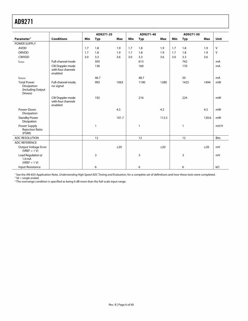
AD9271-25 AD9271-40 AD9271-50 Parameter1 Conditions Min Typ Max Min Typ Max Min Typ Max Unit
POWER SUPPLY AVDD 1.7 1.8 1.9 1.7 1.8 1.9 1.7 1.8 1.9 V DRVDD 1.7 1.8 1.9 1.7 1.8 1.9 1.7 1.8 1.9 V CWVDD 3.0 3.3 3.6 3.0 3.3 3.6 3.0 3.3 3.6 IAVDD Full-channel mode 505 613 742 mA CW Doppler mode
with four channels enabled
136 160 170 mA
IDRVDD 46.7 48.7 50 mA Total Power
Dissipation (Including Output Drivers)
Full-channel mode, no signal
993 1063 1190 1280 1425 1494 mW
CW Doppler mode with four channels enabled
192 216 224 mW
Power-Down Dissipation
4.5 4.5 4.5 mW
Standby Power Dissipation
101.7 112.5 120.6 mW
Power Supply Rejection Ratio (PSRR)
1 1 1 mV/V
ADC RESOLUTION 12 12 12 Bits
ADC REFERENCE Output Voltage Error
(VREF = 1 V) ±20 ±20 ±20 mV
Load Regulation @ 1.0 mA (VREF = 1 V)
3 3 3 mV
Input Resistance 6 6 6 kΩ 1 See the AN-835 Application Note, Understanding High Speed ADC Testing and Evaluation, for a complete set of definitions and how these tests were completed. 2 SE = single ended. 3 The overrange condition is specified as being 6 dB more than the full-scale input range.
AD9271
Rev. B | Page 7 of 60
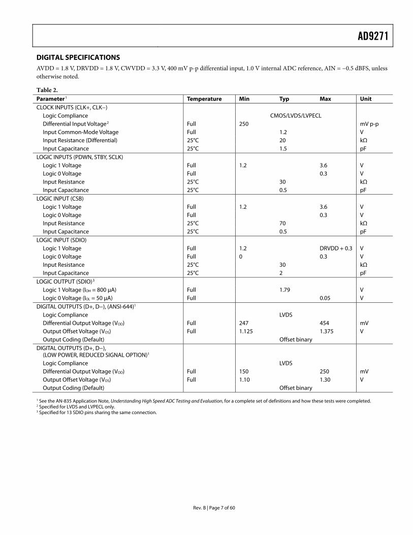
DIGITAL SPECIFICATIONS AVDD = 1.8 V, DRVDD = 1.8 V, CWVDD = 3.3 V, 400 mV p-p differential input, 1.0 V internal ADC reference, AIN = −0.5 dBFS, unless otherwise noted.
Table 2. Parameter1 Temperature Min Typ Max Unit CLOCK INPUTS (CLK+, CLK−)
Logic Compliance CMOS/LVDS/LVPECL Differential Input Voltage2
Full 250 mV p-p Input Common-Mode Voltage Full 1.2 V Input Resistance (Differential) 25°C 20 kΩ Input Capacitance 25°C 1.5 pF
LOGIC INPUTS (PDWN, STBY, SCLK) Logic 1 Voltage Full 1.2 3.6 V Logic 0 Voltage Full 0.3 V Input Resistance 25°C 30 kΩ Input Capacitance 25°C 0.5 pF
LOGIC INPUT (CSB) Logic 1 Voltage Full 1.2 3.6 V Logic 0 Voltage Full 0.3 V Input Resistance 25°C 70 kΩ Input Capacitance 25°C 0.5 pF
LOGIC INPUT (SDIO) Logic 1 Voltage Full 1.2 DRVDD + 0.3 V Logic 0 Voltage Full 0 0.3 V Input Resistance 25°C 30 kΩ Input Capacitance 25°C 2 pF
LOGIC OUTPUT (SDIO)3
Logic 1 Voltage (IOH = 800 μA) Full 1.79 V Logic 0 Voltage (IOL = 50 μA) Full 0.05 V
DIGITAL OUTPUTS (D+, D−), (ANSI-644)1
Logic Compliance LVDS Differential Output Voltage (VOD) Full 247 454 mV Output Offset Voltage (VOS) Full 1.125 1.375 V Output Coding (Default) Offset binary
DIGITAL OUTPUTS (D+, D−), (LOW POWER, REDUCED SIGNAL OPTION)1
Logic Compliance LVDS Differential Output Voltage (VOD) Full 150 250 mV Output Offset Voltage (VOS) Full 1.10 1.30 V Output Coding (Default) Offset binary
1 See the AN-835 Application Note, Understanding High Speed ADC Testing and Evaluation, for a complete set of definitions and how these tests were completed. 2 Specified for LVDS and LVPECL only. 3 Specified for 13 SDIO pins sharing the same connection.
AD9271
Rev. B | Page 8 of 60
SWITCHING SPECIFICATIONS AVDD = 1.8 V, DRVDD = 1.8 V, CWVDD = 3.3 V, 400 mV p-p differential input, 1.0 V internal ADC reference, AIN = −0.5 dBFS, unless otherwise noted.
Table 3. Parameter1 Temp Min Typ Max Unit CLOCK2
Maximum Clock Rate Full 50 MSPS Minimum Clock Rate Full 10 MSPS Clock Pulse Width High (tEH) Full 10.0 ns Clock Pulse Width Low (tEL) Full 10.0 ns
OUTPUT PARAMETERS2, 3
Propagation Delay (tPD) Full 1.5 2.3 3.1 ns Rise Time (tR) (20% to 80%) Full 300 ps Fall Time (tF) (20% to 80%) Full 300 ps FCO Propagation Delay (tFCO) Full 1.5 2.3 3.1 ns DCO Propagation Delay (tCPD)4
Full tFCO + (tSAMPLE/24)
ns
DCO to Data Delay (tDATA)4 Full (tSAMPLE/24) − 300 (tSAMPLE/24) (tSAMPLE/24) + 300 ps
DCO to FCO Delay (tFRAME)4 Full (tSAMPLE/24) − 300 (tSAMPLE/24) (tSAMPLE/24) + 300 ps
Data-to-Data Skew (tDATA-MAX − tDATA-MIN) Full ±50 ±200 ps Wake-Up Time (Standby), VGAIN = 0.5 V 25°C 1 μs Wake-Up Time (Power-Down) 25°C 1 ms Pipeline Latency Full 8 Clock
cycles APERTURE
Aperture Uncertainty (Jitter) 25°C <1 ps rms 1 See the AN-835 Application Note, Understanding High Speed ADC Testing and Evaluation, for a complete set of definitions and how these tests were completed. 2 Can be adjusted via the SPI interface. 3 Measurements were made using a part soldered to FR-4 material. 4 tSAMPLE/24 is based on the number of bits divided by 2, because the delays are based on half duty cycles.
AD9271
Rev. B | Page 9 of 60
ADC TIMING DIAGRAMS
DCO–
DCO+
DOUTx–
FCO–
FCO+
AIN
CLK–
CLK+
MSB D10 D9 D8 D7 D6 D5 D4 D3 D2 D1 D0 D10MSB
DOUTx+
N – 9 N – 9 N – 9 N – 9 N – 9 N – 9 N – 9 N – 9 N – 9 N – 9 N – 9 N – 9 N – 8N – 8
0630
4-00
N – 1
N
tDATA
tFRAMEtFCO
tPD
tEH
tA
2
tCPD
tEL
Figure 2. 12-Bit Data Serial Stream (Default)
DCO–
DCO+
DOUTx–
DOUTx+
FCO–
FCO+
AIN
CLK–
CLK+
LSBN – 9
D0N – 9
D1N – 9
D2N – 9
D3N – 9
D4N – 9
D5N – 9
D6N – 9
D7N – 9
D8N – 9
D9N – 9
D10N – 9
D0N – 8
LSBN – 8
N – 1
tA
N
tDATA
tFRAMEtFCO
tPD
tEH
0630
4-00
4
tCPD
tEL
Figure 3. 12-Bit Data Serial Stream, LSB First
AD9271
Rev. B | Page 10 of 60
ABSOLUTE MAXIMUM RATINGS Table 4. Stresses above those listed under Absolute Maximum Ratings may cause permanent damage to the device. This is a stress rating only; functional operation of the device at these or any other conditions above those indicated in the operational section of this specification is not implied. Exposure to absolute maximum rating conditions for extended periods may affect device reliability.
Parameter With Respect To Rating
ELECTRICAL AVDD GND −0.3 V to +2.0 V DRVDD GND −0.3 V to +2.0 V CWVDD GND −0.3 V to +3.9 V GND GND −0.3 V to +0.3 V AVDD DRVDD −2.0 V to +2.0 V Digital Outputs
(DOUTx+, DOUTx−, DCO+, DCO−, FCO+, FCO−)
GND −0.3 V to +2.0 V
CLK+, CLK− GND −0.3 V to +3.9 V LI-x LG-x −0.3 V to +2.0 V LO-x LG-x −0.3 V to +2.0 V LOSW-x LG-x −0.3 V to +2.0 V CWDx−, CWDx+ GND −0.3 V to +3.9 V SDIO, GAIN+, GAIN− GND −0.3 V to +2.0 V PDWN, STBY, SCLK, CSB GND −0.3 V to +3.9 V REFT, REFB, RBIAS GND −0.3 V to +2.0 V VREF, SENSE GND −0.3 V to +2.0 V
ENVIRONMENTAL Operating Temperature
Range (Ambient) −40°C to +85°C
Storage Temperature Range (Ambient)
−65°C to +150°C
Maximum Junction Temperature
150°C
Lead Temperature (Soldering, 10 sec)
300°C
THERMAL IMPEDANCE
Table 5. Air Flow Velocity (m/s) θJA
1 θJB θJC Unit 0.0 20.3 °C/W 1.0 14.4 7.6 4.7 °C/W 2.5 12.9 °C/W 1 θJA for a 4-layer PCB with solid ground plane (simulated). Exposed pad
soldered to PCB.
ESD CAUTION
AD9271
Rev. B | Page 11 of 60
LI-FLG-F
LO-F
LI-GLG-G
LO-G
AVDD
CLK–CLK+
AVDD
AVDD
AVDD
AVDD
LI-ELG-E
AVDD
AVDD
LI-HLG-H
LO-H
AVDDAVDD
LOSW-F
LOSW-
PIN CONFIGURATION AND FUNCTION DESCRIPTIONS
G
LOSW-H
0630
4-00
5
AD9271TOP VIEW
(Not to Scale)
EXPOSED PADDLE, PIN 0(BOTTOM OF PACKAGE)
PIN 1INDICATOR
1
2
3
4
5
6
7
8
9
10
11
12
13
14
15
16
17
18
19
20
21
22
23
24
25
5026 27 28 29 30 31 32 33 34 35 36 37 38 39 40 41 42 43 44 45 46 47 48 49
100
99 98 97 96 95 94 93 92 91 90 89 88 87 86 85 84 83 82 81 80 79 78 77 76A
VDD
74
75
PDW
N
73
STB
Y
72
DR
VDD
71
DO
UTA
+
70
DO
UTA
–
69
DO
UTB
+
68
DO
UTB
–
67
DO
UTC
+
66
DO
UTC
–
65
DO
UTD
+
64
DO
UTD
–
63
FCO
+
62
FCO
–61
DC
O+
60
DC
O–
59
DO
UTE
+
58
DO
UTE
–
57
DO
UTF
+
56
DO
UTF
–
55
DO
UTG
+
54
DO
UTG
–
53
DO
UTH
+
52
DO
UTH
–
51
DR
VDD
AVDD
LI-ALG-A
LOSW-A
LI-BLG-B
LO-B
AVDD
SDIOSCLK
CSB
AVDD
AVDD
LI-CLG-C
LO-C
AVDDAVDD
LI-DLG-D
AVDDAVDD
LO-A
LOSW-B
LOSW-C
LOSW
-DLO
-DC
WD
0–C
WD
0+C
WD
1–C
WD
1+C
WD
2–C
WD
2+C
WVD
DG
AIN
–G
AIN
+R
BIA
SSE
NSE
VREF
REF
BR
EFT
AVD
DC
WD
3–C
WD
3+C
WD
4–C
WD
4+C
WD
5–C
WD
5+LO
-ELO
SW-E
Figure 4. 100-Lead TQFP Pin Configuration
Table 6. Pin Function Descriptions Pin No. Name Description 0 GND Ground (exposed paddle should be tied to a quiet analog ground) 3, 4, 9, 10, 15, 16, 21, 22, 25, 50, 54, 55, 60, 61, 66, 67, 72, 73, 92
AVDD 1.8 V Analog Supply
26, 47 DRVDD 1.8 V Digital Output Driver Supply 84 CWVDD 3.3 V Analog Supply 1 LI-E LNA Analog Input for Channel E 2 LG-E LNA Ground for Channel E 5 LO-F LNA Analog Output for Channel F 6 LOSW-F LNA Analog Output Complement for Channel F 7 LI-F LNA Analog Input for Channel F 8 LG-F LNA Ground for Channel F 11 LO-G LNA Analog Output for Channel G 12 LOSW-G LNA Analog Output Complement for Channel G 13 LI-G LNA Analog Input for Channel G 14 LG-G LNA Ground for Channel G 17 LO-H LNA Analog Output for Channel H
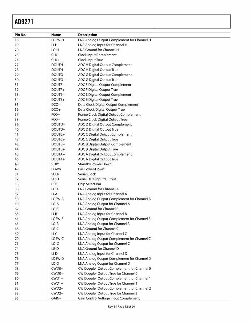
AD9271
Rev. B | Page 12 of 60
Pin No. Name Description 18 LOSW-H LNA Analog Output Complement for Channel H 19 LI-H LNA Analog Input for Channel H 20 LG-H LNA Ground for Channel H 23 CLK− Clock Input Complement 24 CLK+ Clock Input True 27 DOUTH− ADC H Digital Output Complement 28 DOUTH+ ADC H Digital Output True 29 DOUTG− ADC G Digital Output Complement 30 DOUTG+ ADC G Digital Output True 31 DOUTF− ADC F Digital Output Complement 32 DOUTF+ ADC F Digital Output True 33 DOUTE− ADC E Digital Output Complement 34 DOUTE+ ADC E Digital Output True 35 DCO− Data Clock Digital Output Complement 36 DCO+ Data Clock Digital Output True 37 FCO− Frame Clock Digital Output Complement 38 FCO+ Frame Clock Digital Output True 39 DOUTD− ADC D Digital Output Complement 40 DOUTD+ ADC D Digital Output True 41 DOUTC− ADC C Digital Output Complement 42 DOUTC+ ADC C Digital Output True 43 DOUTB− ADC B Digital Output Complement 44 DOUTB+ ADC B Digital Output True 45 DOUTA− ADC A Digital Output Complement 46 DOUTA+ ADC A Digital Output True 48 STBY Standby Power-Down 49 PDWN Full Power-Down 51 SCLK Serial Clock 52 SDIO Serial Data Input/Output 53 CSB Chip Select Bar 56 LG-A LNA Ground for Channel A 57 LI-A LNA Analog Input for Channel A 58 LOSW-A LNA Analog Output Complement for Channel A 59 LO-A LNA Analog Output for Channel A 62 LG-B LNA Ground for Channel B 63 LI-B LNA Analog Input for Channel B 64 LOSW-B LNA Analog Output Complement for Channel B 65 LO-B LNA Analog Output for Channel B 68 LG-C LNA Ground for Channel C 69 LI-C LNA Analog Input for Channel C 70 LOSW-C LNA Analog Output Complement for Channel C 71 LO-C LNA Analog Output for Channel C 74 LG-D LNA Ground for Channel D 75 LI-D LNA Analog Input for Channel D 76 LOSW-D LNA Analog Output Complement for Channel D 77 LO-D LNA Analog Output for Channel D 78 CWD0− CW Doppler Output Complement for Channel 0 79 CWD0+ CW Doppler Output True for Channel 0 80 CWD1− CW Doppler Output Complement for Channel 1 81 CWD1+ CW Doppler Output True for Channel 1 82 CWD2− CW Doppler Output Complement for Channel 2 83 CWD2+ CW Doppler Output True for Channel 2 85 GAIN− Gain Control Voltage Input Complement
AD9271
Rev. B | Page 13 of 60
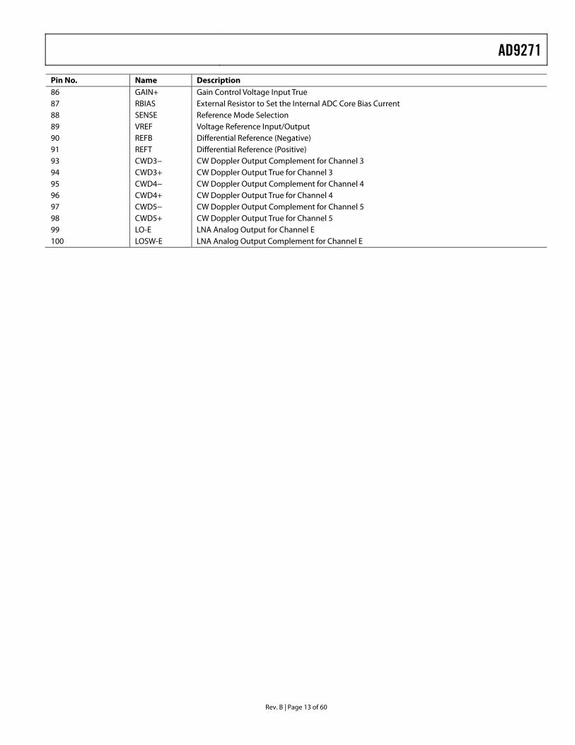
Pin No. Name Description 86 GAIN+ Gain Control Voltage Input True 87 RBIAS External Resistor to Set the Internal ADC Core Bias Current 88 SENSE Reference Mode Selection 89 VREF Voltage Reference Input/Output 90 REFB Differential Reference (Negative) 91 REFT Differential Reference (Positive) 93 CWD3− CW Doppler Output Complement for Channel 3 94 CWD3+ CW Doppler Output True for Channel 3 95 CWD4− CW Doppler Output Complement for Channel 4 96 CWD4+ CW Doppler Output True for Channel 4 97 CWD5− CW Doppler Output Complement for Channel 5 98 CWD5+ CW Doppler Output True for Channel 5 99 LO-E LNA Analog Output for Channel E 100 LOSW-E LNA Analog Output Complement for Channel E
AD9271
Rev. B | Page 14 of 60
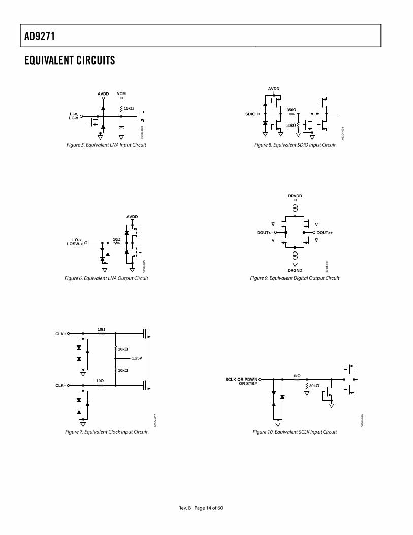
LI-x,LG-x
15kΩ
EQUIVALENT CIRCUITS
AVDD VCM
0630
4-07
3
Figure 5. Equivalent LNA Input Circuit
LO-x,LOSW-x
10Ω
0630
4-07
5
AVDD
Figure 6. Equivalent LNA Output Circuit
10Ω
10kΩ
10kΩ
CLK–10Ω
1.25V
CLK+
0630
4-00
7
Figure 7. Equivalent Clock Input Circuit
SDIO350Ω
30kΩ
0630
4-00
8
AVDD
Figure 8. Equivalent SDIO Input Circuit
DRVDD
DRGND
DOUTx– DOUTx+
V
V
V
V
0630
4-00
9
Figure 9. Equivalent Digital Output Circuit
SCLK OR PDWNOR STBY 30kΩ
1kΩ
0630
4-01
0
Figure 10. Equivalent SCLK Input Circuit
AD9271
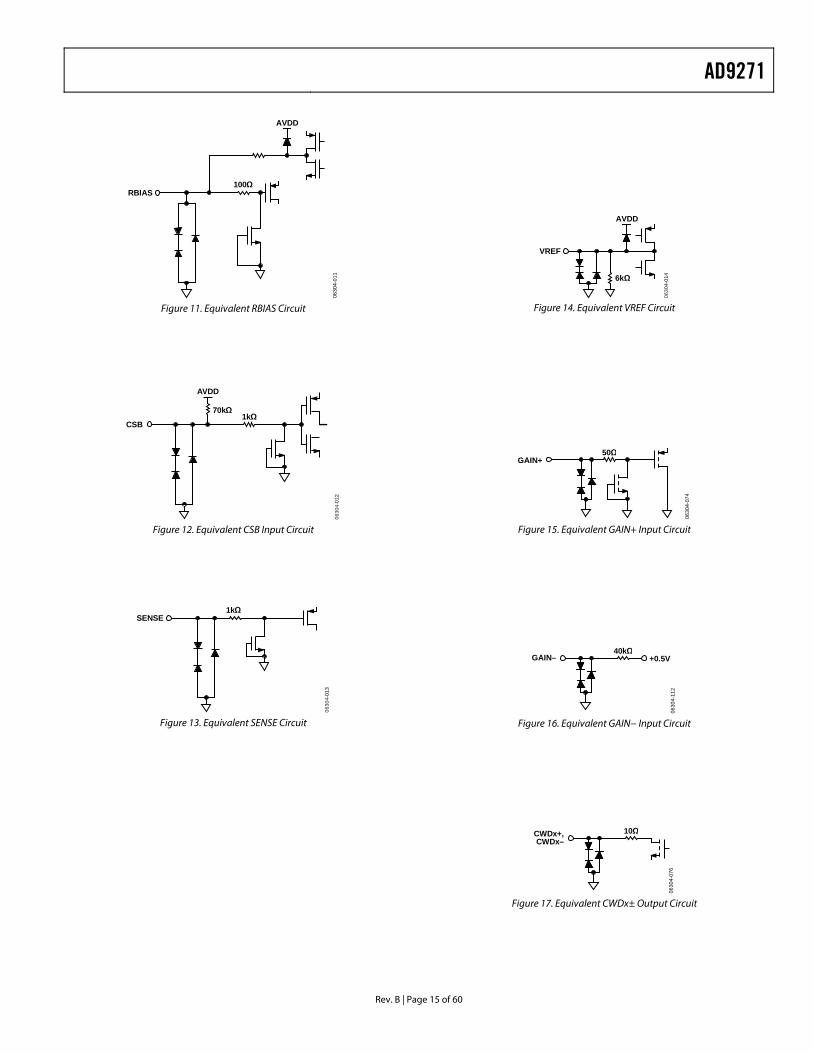
Rev. B | Page 15 of 60
100ΩRBIAS
AVDD
Figure 11. Equivalent RBIAS Circuit
CSB
70kΩ1kΩ
AVDD
0630
4-01
106
304-
012
Figure 12. Equivalent CSB Input Circuit
SENSE1kΩ
0630
4-01
3
Figure 13. Equivalent SENSE Circuit
VREF
6kΩ
0630
4-01
4
AVDD
Figure 14. Equivalent VREF Circuit
GAIN+50Ω
0630
4-07
4
Figure 15. Equivalent GAIN+ Input Circuit
GAIN– +0.5V40kΩ
0630
4-11
2
Figure 16. Equivalent GAIN− Input Circuit
CWDx+,CWDx–
10Ω
0630
4-07
6
Figure 17. Equivalent CWDx± Output Circuit
AD9271
Rev. B | Page 16 of 60
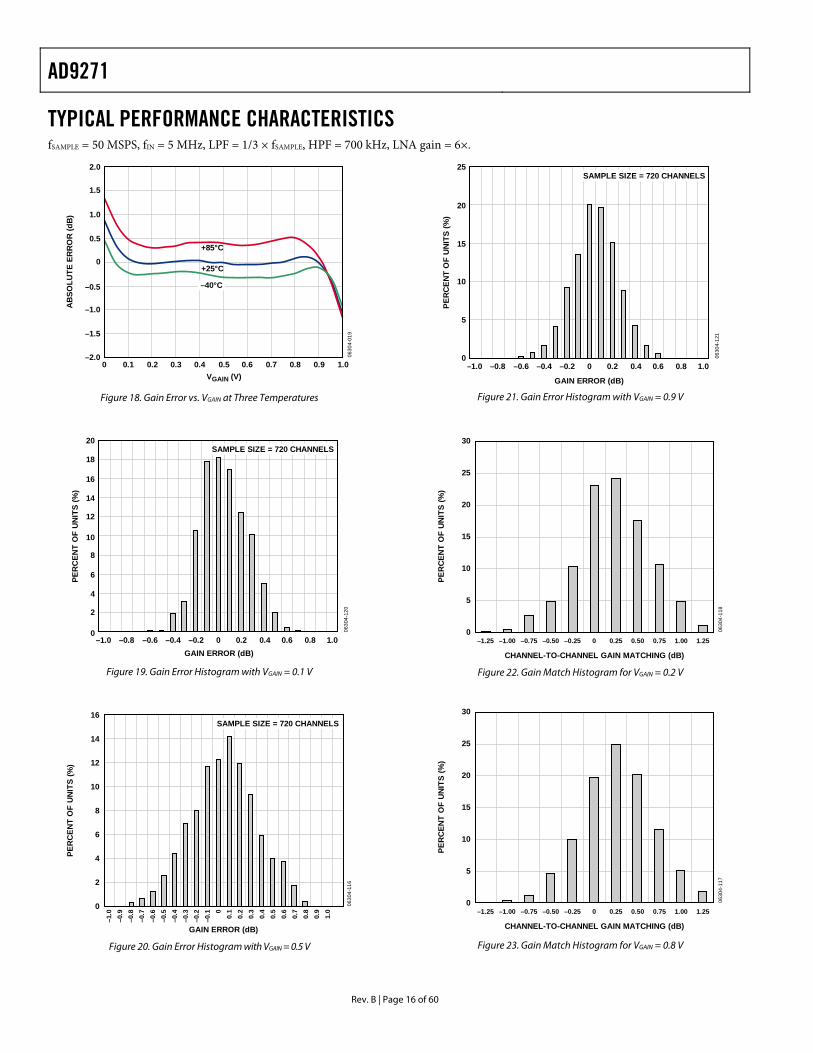
–2.0 0630
VGAIN (V)
TYPICAL PERFORMANCE CHARACTERISTICS fSAMPLE = 50 MSPS, fIN = 5 MHz, LPF = 1/3 × fSAMPLE, HPF = 700 kHz, LNA gain = 6×.
2.0
1.0
1.5
–1.0
–0.5
0
0.5
–1.5
4-01
9
AB
SOLU
TE E
RR
OR
(dB
)
0 0.1 0.2 0.3 0.4 0.5 0.6 0.7 0.8 0.9 1.0
+85°C
+25°C
–40°C
Figure 18. Gain Error vs. VGAIN at Three Temperatures
20
10
4-12
0
PER
CEN
T O
F U
NIT
S (%
)
18
16
14
12
8
6
4
2
–1.0 –0.6
0630
GAIN ERROR (dB)
0–0.8 –0.4 –0.2 0 0.40.2 0.6 0.8 1.0
SAMPLE SIZE = 720 CHANNELS
Figure 19. Gain Error Histogram with VGAIN = 0.1 V
06
GAIN ERROR (dB)
–1.0
–0.9
–0.8
–0.7
–0.6
–0.5
–0.4
–0.3
–0.2
–0.1 0
0.1
0.2
0.3
0.4
0.5
0.6
0.7
0.8
0.9
1.00
304-
116
PER
CEN
T O
F U
NIT
S (%
)
16
14
12
10
8
6
4
2
SAMPLE SIZE = 720 CHANNELS
Figure 20. Gain Error Histogram with VGAIN = 0.5 V
25
0–1.0 –0.6
0630
4-12
1
GAIN ERROR (dB)
PER
CEN
T O
F U
NIT
S (%
)
20
15
10
5
–0.8 –0.4 –0.2 0 0.40.2 0.6 0.8 1.0
SAMPLE SIZE = 720 CHANNELS
Figure 21. Gain Error Histogram with VGAIN = 0.9 V
0630
4-11
8
PER
CEN
T O
F U
NIT
S (%
)
CHANNEL-TO-CHANNEL GAIN MATCHING (dB)
0
30
25
20
15
10
–1.25 –1.00 –0.75 –0.50 –0.25 0 0.25 0.50 0.75 1.00 1.25
5
Figure 22. Gain Match Histogram for VGAIN = 0.2 V
0630
4-11
7
PER
CEN
T O
F U
NIT
S (%
)
CHANNEL-TO-CHANNEL GAIN MATCHING (dB)
0
30
25
20
15
10
–1.25 –1.00 –0.75 –0.50 –0.25 0 0.25 0.50 0.75 1.00 1.25
5
Figure 23. Gain Match Histogram for VGAIN = 0.8 V
AD9271
Rev. B | Page 17 of 60
0630
4-02
2
CODES
NU
MB
ER O
F H
ITS
–5 –4 –3 –2 –1 0 1 2 3 4 50
200000
0630
4-02
3
CODES–5 –4 –3 –2 –1 0 1 2 3 4 5
0
400000
600000
800000
1000000
1200000
1400000
1600000
1800000
2000000
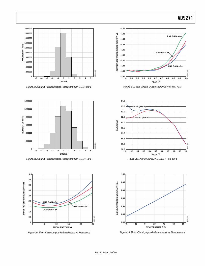
Figure 24. Output-Referred Noise Histogram with VGAIN = 0.0 V
NU
MB
ER O
F H
ITS
200000
400000
600000
800000
1000000
1200000
Figure 25. Output-Referred Noise Histogram with VGAIN = 1.0 V
0630
4-02
5
FREQUENCY (MHz)0 5 10 15 20 25
0
0.5
INPU
T-R
EFER
RED
NO
ISE
(nV/
Hz)
1.0
1.5
2.0
2.5
3.0
3.5
4.0
4.5
LNA GAIN = 5×
LNA GAIN = 8×LNA GAIN = 6×
Figure 26. Short-Circuit, Input-Referred Noise vs. Frequency
0630
4-02
1OU
TPU
T-R
EFER
RED
NO
ISE
(dB
FS/
Hz)
VGAIN (V)0 0.1 0.2 0.3 0.4 0.5 0.6 0.7 0.8 0.9 1.0
–140
–139
–138
–137
–136
–135
–134
–133
–132
–131
LNA GAIN = 5×
LNA GAIN = 6×
LNA GAIN = 8×
Figure 27. Short-Circuit, Output-Referred Noise vs. VGAIN
0 0.1 0.2 0.3 0.4 0.5 0.6 0.7 0.8 0.9 1.0
0630
4-02
0
SNR
/SIN
AD
VGAIN (V)
59.5
60.0
60.5
61.0
61.5
62.0
62.5
63.0
63.5
64.0
SNR (dBFS)
SINAD (dBFS)
Figure 28. SNR/SINAD vs. VGAIN, AIN = −6.5 dBFS
0630
4-02
4
INPU
T-R
EFER
RED
NO
ISE
(nV/
Hz)
TEMPERATURE (°C)–40 –20 0 20 40 60 80
1.40
1.45
1.50
1.55
1.60
1.65
1.70
Figure 29. Short-Circuit, Input-Referred Noise vs. Temperature
AD9271
Rev. B | Page 18 of 60
0
–15
–10
–5
–25
–20
–30
FUN
DA
MEN
TAL
(dB
FS)
–35
–400 2.5 5.0 7.5 10.0 12.5 15.0 17.5 20.0 22.5 25.0
0630
4-03
0
FREQUENCY (MHz)
–3dB LINE (1/3) × 50MSPS
(1/3) × 40MSPS
(1/3) × 25MSPS
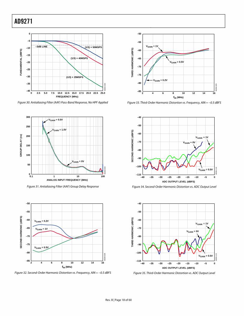
Figure 30. Antialiasing Filter (AAF) Pass-Band Response, No HPF Applied
300
50
100
150
200
250
GR
OU
P D
ELA
Y (n
s)
00.1 1 10 100
0630
4-03
3
ANALOG INPUT FREQUENCY (MHz)
VGAIN = 0V
VGAIN = 1.0V
VGAIN = 0.5V
Figure 31. Antialiasing Filter (AAF) Group Delay Response
0630
4-02
8
fIN (MHz)
2 4 6 8 10 12 14 16–85
SEC
ON
D H
AR
MO
NIC
(dB
FS)
–80
–75
–70
–65
–60
–55
–50
VGAIN = 0.2V
VGAIN = 0.5V
VGAIN = 1V
Figure 32. Second-Order Harmonic Distortion vs. Frequency, AIN = −0.5 dBFS
0630
4-02
9
THIR
D H
AR
MO
NIC
(dB
FS)
fIN (MHz)
2 4 6 8 10 12 14 1–85
–80
–75
–70
–65
–60
–55
6
–50
VGAIN = 0.2V
VGAIN = 1V
VGAIN = 0.5V
Figure 33. Third-Order Harmonic Distortion vs. Frequency, AIN = −0.5 dBFS
0630
4-11
4
SEC
ON
D H
AR
MO
NIC
(dB
FS)
ADC OUTPUT LEVEL (dBFS)
–110
–40
–50
–60
–70
–80
–90
–100
–40 0–5–10–15–20–25–30–35
VGAIN = 0V
VGAIN = 0.5V
VGAIN = 1V
Figure 34. Second-Order Harmonic Distortion vs. ADC Output Level
0630
4-11
5
THIR
D H
AR
MO
NIC
(dB
FS)
ADC OUTPUT LEVEL (dBFS)
–110
–40
–50
–60
–70
–80
–90
–100
–40 0–5–10–15–20–25–30–35
VGAIN = 0V
VGAIN = 0.5V
VGAIN = 1V
Figure 35. Third-Order Harmonic Distortion vs. ADC Output Level
AD9271
Rev. B | Page 19 of 60
–110
–100
–90
–80
–70
–60
–50
–40
–30
–20
–10
0
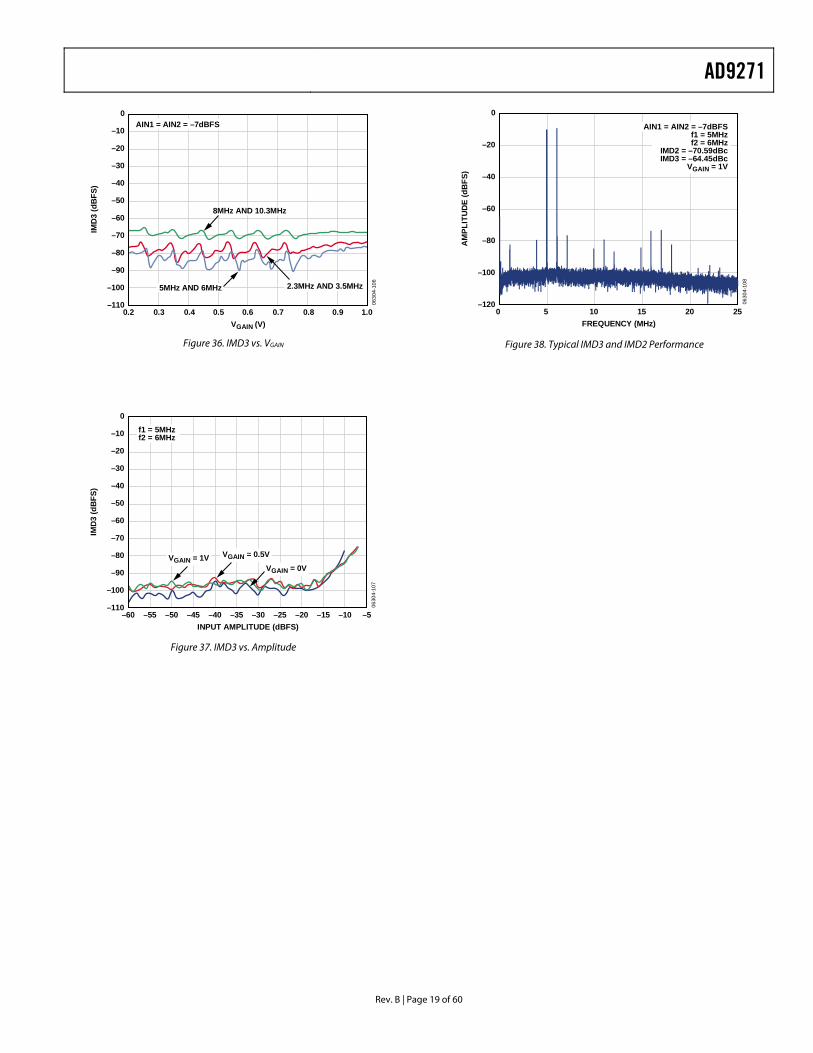
2.3MHz AND 3.5MHz 5MHz AND 6MHz
8MHz AND 10.3MHz
0.2 1.00.90.80.70.60.50.40.3
0630
4-10
6
VGAIN (V)
IMD
3 (d
BFS
)
AIN1 = AIN2 = –7dBFS
Figure 36. IMD3 vs. VGAIN
–110
–100
–60 –20 –15 –10 –5–25–30–35–40–45–50–55
0630
4-10
7
INPUT AMPLITUDE (dBFS)
–90
–80
–70
–60
–50
–40
–30
–20
–10
0
IMD
3 (d
BFS
)
VGAIN = 1V VGAIN = 0.5V
VGAIN = 0V
f1 = 5MHzf2 = 6MHz
Figure 37. IMD3 vs. Amplitude
–120
–100
–80
–60
–40
–20
0
0 22015105
0630
4-10
8
AM
PLIT
UD
E (d
BFS
)
FREQUENCY (MHz)5
AIN1 = AIN2 = –7dBFSf1 = 5MHzf2 = 6MHz
IMD2 = –70.59dBcIMD3 = –64.45dBc
VGAIN = 1V
Figure 38. Typical IMD3 and IMD2 Performance
AD9271
Rev. B | Page 20 of 60
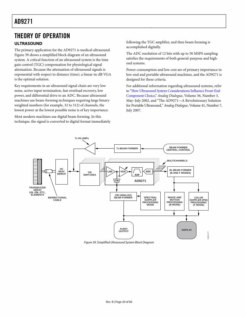
THEORY OF OPERATION ULTRASOUND The primary application for the AD9271 is medical ultrasound. Figure 39 shows a simplified block diagram of an ultrasound system. A critical function of an ultrasound system is the time gain control (TGC) compensation for physiological signal attenuation. Because the attenuation of ultrasound signals is exponential with respect to distance (time), a linear-in-dB VGA is the optimal solution.
Key requirements in an ultrasound signal chain are very low noise, active input termination, fast overload recovery, low power, and differential drive to an ADC. Because ultrasound machines use beam-forming techniques requiring large binary-weighted numbers (for example, 32 to 512) of channels, the lowest power at the lowest possible noise is of key importance.
Most modern machines use digital beam forming. In this technique, the signal is converted to digital format immediately
following the TGC amplifier, and then beam forming is accomplished digitally.
The ADC resolution of 12 bits with up to 50 MSPS sampling satisfies the requirements of both general-purpose and high-end systems.
Power consumption and low cost are of primary importance in low-end and portable ultrasound machines, and the AD9271 is designed for these criteria.
For additional information regarding ultrasound systems, refer to “How Ultrasound System Considerations Influence Front-End Component Choice,” Analog Dialogue, Volume 36, Number 3, May–July 2002, and “The AD9271—A Revolutionary Solution for Portable Ultrasound,” Analog Dialogue, Volume 41, Number 7, July 2007.
Tx HV
BEAM FORMERCENTRAL CONTROL
Rx BEAM FORMER(B AND F MODES)
COLORDOPPLER (PW)PROCESSING
(F MODE)
IMAGE ANDMOTION
PROCESSING(B MODE)
SPECTRALDOPPLER
PROCESSINGMODE
DISPLAYAUDIOOUTPUT
Tx BEAM FORMER
CW (ANALOG)BEAM FORMER
AMPs
MULTICHANNELS
TRANSDUCERARRAY
128, 256, ETC.,ELEMENTS
BIDIRECTIONALCABLE
HVMUX/
DEMUX T/RSWITCHES
0630
4-07
7
AD9271
AAFVGA ADCLNA
CW
Figure 39. Simplified Ultrasound System Block Diagram
AD9271
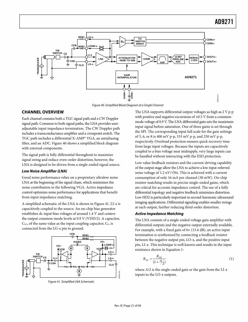
Rev. B | Page 21 of 60
LNALI-x
LG-x
LO-x
DOUTx+
DOUTx–CS
T/RSWITCH
CLG
CFB RFB2
CSH
GAININTERPOLATOR
LOSW-x
RFB1TO
SWITCHARRAY
gmCDWx+CDWx–
ATTENUATOR–30dB TO 0dB
12-BITPIPELINE
ADCSERIALLVDS+24dB
GA
IN–
0630
4-07
1
AAF
GA
IN+
AD9271
TRA
NSD
UC
ER
Figure 40. Simplified Block Diagram of a Single Channel
CHANNEL OVERVIEW Each channel contains both a TGC signal path and a CW Doppler signal path. Common to both signal paths, the LNA provides user-adjustable input impedance termination. The CW Doppler path includes a transconductance amplifier and a crosspoint switch. The TGC path includes a differential X-AMP® VGA, an antialiasing filter, and an ADC. Figure 40 shows a simplified block diagram with external components.
The signal path is fully differential throughout to maximize signal swing and reduce even-order distortion; however, the LNA is designed to be driven from a single-ended signal source.
Low Noise Amplifier (LNA)
Good noise performance relies on a proprietary ultralow noise LNA at the beginning of the signal chain, which minimizes the noise contribution in the following VGA. Active impedance control optimizes noise performance for applications that benefit from input impedance matching.
A simplified schematic of the LNA is shown in Figure 41. LI-x is capacitively coupled to the source. An on-chip bias generator establishes dc input bias voltages of around 1.4 V and centers the output common-mode levels at 0.9 V (VDD/2). A capacitor, CLG, of the same value as the input coupling capacitor, CS, is connected from the LG-x pin to ground.
LI-xCS
CLG
CFB
CSH
LG-x
LO-x
LOSW-xVCMVCM
VO+VO–
RFB1RFB2
0630
4-10
1
T/RSWITCH
TRA
NSD
UC
ER
AVDD2
Figure 41. Simplified LNA Schematic
The LNA supports differential output voltages as high as 2 V p-p with positive and negative excursions of ±0.5 V from a common-mode voltage of 0.9 V. The LNA differential gain sets the maximum input signal before saturation. One of three gains is set through the SPI. The corresponding input full scale for the gain settings of 5, 6, or 8 is 400 mV p-p, 333 mV p-p, and 250 mV p-p, respectively. Overload protection ensures quick recovery time from large input voltages. Because the inputs are capacitively coupled to a bias voltage near midsupply, very large inputs can be handled without interacting with the ESD protection.
Low value feedback resistors and the current-driving capability of the output stage allow the LNA to achieve a low input-referred noise voltage of 1.2 nV/√Hz. This is achieved with a current consumption of only 16 mA per channel (30 mW). On-chip resistor matching results in precise single-ended gains, which are critical for accurate impedance control. The use of a fully differential topology and negative feedback minimizes distortion. Low HD2 is particularly important in second-harmonic ultrasound imaging applications. Differential signaling enables smaller swings at each output, further reducing third-order distortion.
Active Impedance Matching
The LNA consists of a single-ended voltage gain amplifier with differential outputs and the negative output externally available. For example, with a fixed gain of 6× (15.6 dB), an active input termination is synthesized by connecting a feedback resistor between the negative output pin, LO-x, and the positive input pin, LI-x. This technique is well known and results in the input resistance shown in Equation 1:
)21( AR
R FBIN += (1)
where A/2 is the single-ended gain or the gain from the LI-x inputs to the LO-x outputs.
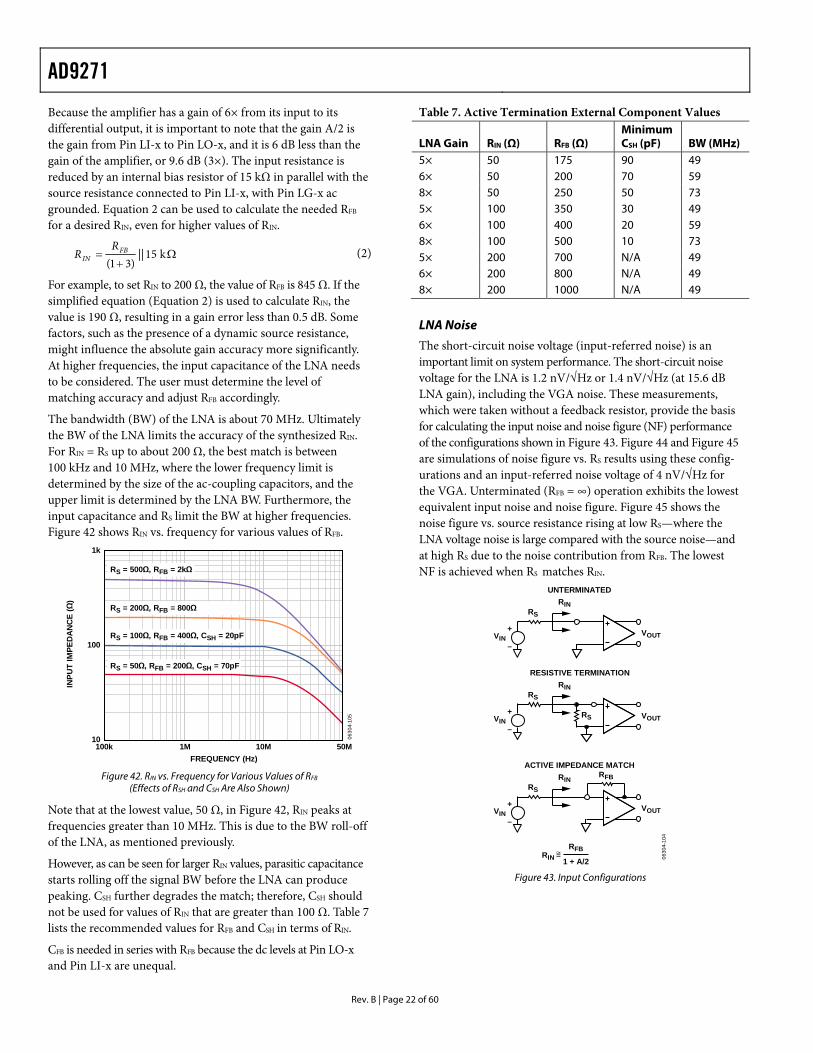
AD9271
Rev. B | Page 22 of 60
Because the amplifier has a gain of 6× from its input to its differential output, it is important to note that the gain A/2 is the gain from Pin LI-x to Pin LO-x, and it is 6 dB less than the gain of the amplifier, or 9.6 dB (3×). The input resistance is reduced by an internal bias resistor of 15 kΩ in parallel with the source resistance connected to Pin LI-x, with Pin LG-x ac grounded. Equation 2 can be used to calculate the needed RFB for a desired RIN, even for higher values of RIN.
Ω+
= k15||)31(
FBIN
RR (2)
For example, to set RIN to 200 Ω, the value of RFB is 845 Ω. If the simplified equation (Equation 2) is used to calculate RIN, the value is 190 Ω, resulting in a gain error less than 0.5 dB. Some factors, such as the presence of a dynamic source resistance, might influence the absolute gain accuracy more significantly. At higher frequencies, the input capacitance of the LNA needs to be considered. The user must determine the level of matching accuracy and adjust RFB accordingly.
The bandwidth (BW) of the LNA is about 70 MHz. Ultimately the BW of the LNA limits the accuracy of the synthesized RIN. For RIN = RS up to about 200 Ω, the best match is between 100 kHz and 10 MHz, where the lower frequency limit is determined by the size of the ac-coupling capacitors, and the upper limit is determined by the LNA BW. Furthermore, the input capacitance and RS limit the BW at higher frequencies. Figure 42 shows RIN vs. frequency for various values of RFB.
0630
4-10
10100k 1M 10M 50M
FREQUENCY (Hz)
5
100
1k
INPU
T IM
PED
AN
CE
(Ω)
RS = 50Ω, RFB = 200Ω, CSH = 70pF
RS = 100Ω, RFB = 400Ω, CSH = 20pF
RS = 200Ω, RFB = 800Ω
RS = 500Ω, RFB = 2kΩ
Figure 42. RIN vs. Frequency for Various Values of RFB
(Effects of RSH and CSH Are Also Shown)
Note that at the lowest value, 50 Ω, in Figure 42, RIN peaks at frequencies greater than 10 MHz. This is due to the BW roll-off of the LNA, as mentioned previously.
However, as can be seen for larger RIN values, parasitic capacitance starts rolling off the signal BW before the LNA can produce peaking. CSH further degrades the match; therefore, CSH should not be used for values of RIN that are greater than 100 Ω. Table 7 lists the recommended values for RFB and CSH in terms of RIN.
CFB is needed in series with RFB because the dc levels at Pin LO-x and Pin LI-x are unequal.
Table 7. Active Termination External Component Values
LNA Gain RIN (Ω) RFB (Ω) Minimum CSH (pF) BW (MHz)
5× 50 175 90 49 6× 50 200 70 59 8× 50 250 50 73 5× 100 350 30 49 6× 100 400 20 59 8× 100 500 10 73 5× 200 700 N/A 49 6× 200 800 N/A 49 8× 200 1000 N/A 49
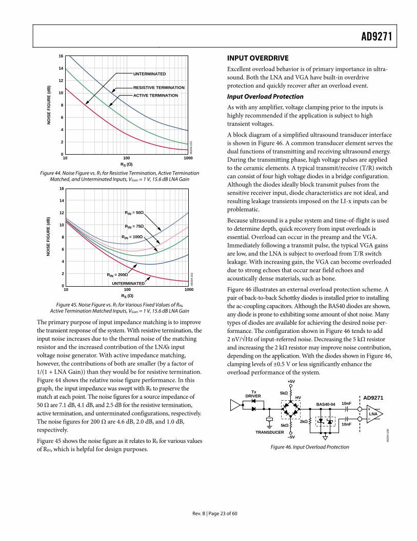
LNA Noise
The short-circuit noise voltage (input-referred noise) is an important limit on system performance. The short-circuit noise voltage for the LNA is 1.2 nV/√Hz or 1.4 nV/√Hz (at 15.6 dB LNA gain), including the VGA noise. These measurements, which were taken without a feedback resistor, provide the basis for calculating the input noise and noise figure (NF) performance of the configurations shown in Figure 43. Figure 44 and Figure 45 are simulations of noise figure vs. RS results using these config-urations and an input-referred noise voltage of 4 nV/√Hz for the VGA. Unterminated (RFB = ∞) operation exhibits the lowest equivalent input noise and noise figure. Figure 45 shows the noise figure vs. source resistance rising at low RS—where the LNA voltage noise is large compared with the source noise—and at high RS due to the noise contribution from RFB. The lowest NF is achieved when RS matches RIN.
VOUT
UNTERMINATED
+
–VIN
RINRS
VOUT
RESISTIVE TERMINATION
+
–VIN
RINRS
RS
VOUT
ACTIVE IMPEDANCE MATCH
+
–VIN
RINRFB
RFB
1 + A/2
RS
RIN = 0630
4-10
4
Figure 43. Input Configurations
AD9271
Rev. B | Page 23 of 60
0 0630
4-10
3
NO
ISE
FIG
UR
E (d
B)
2
4
6
8
10
12
14
16
10 100 1000RS (Ω)
UNTERMINATED
RESISTIVE TERMINATION
ACTIVE TERMINATION
Figure 44. Noise Figure vs. RS for Resistive Termination, Active Termination
Matched, and Unterminated Inputs, VGain = 1 V, 15.6 dB LNA Gain
0630
4-1
010 100 1000
RS (Ω)
022
4
6
8
10
12
14
16
NO
ISE
FIG
UR
E (d
B)
RIN = 50Ω
RIN = 100Ω
RIN = 75Ω
R = 200ΩIN
UNTERMINATED
Figure 45. Noise Figure vs. RS for Various Fixed Values of RIN,
Active Termination Matched Inputs, VGain = 1 V, 15.6 dB LNA Gain
The primary purpose of input impedance matching is to improve the transient response of the system. With resistive termination, the input noise increases due to the thermal noise of the matching resistor and the increased contribution of the LNA’s input voltage noise generator. With active impedance matching, however, the contributions of both are smaller (by a factor of 1/(1 + LNA Gain)) than they would be for resistive termination. Figure 44 shows the relative noise figure performance. In this graph, the input impedance was swept with RS to preserve the match at each point. The noise figures for a source impedance of 50 Ω are 7.1 dB, 4.1 dB, and 2.5 dB for the resistive termination, active termination, and unterminated configurations, respectively. The noise figures for 200 Ω are 4.6 dB, 2.0 dB, and 1.0 dB, respectively.
Figure 45 shows the noise figure as it relates to RS for various values of RIN, which is helpful for design purposes.
INPUT OVERDRIVE Excellent overload behavior is of primary importance in ultra-sound. Both the LNA and VGA have built-in overdrive protection and quickly recover after an overload event.
Input Overload Protection
As with any amplifier, voltage clamping prior to the inputs is highly recommended if the application is subject to high transient voltages.
A block diagram of a simplified ultrasound transducer interface is shown in Figure 46. A common transducer element serves the dual functions of transmitting and receiving ultrasound energy. During the transmitting phase, high voltage pulses are applied to the ceramic elements. A typical transmit/receive (T/R) switch can consist of four high voltage diodes in a bridge configuration. Although the diodes ideally block transmit pulses from the sensitive receiver input, diode characteristics are not ideal, and resulting leakage transients imposed on the LI-x inputs can be problematic.
Because ultrasound is a pulse system and time-of-flight is used to determine depth, quick recovery from input overloads is essential. Overload can occur in the preamp and the VGA. Immediately following a transmit pulse, the typical VGA gains are low, and the LNA is subject to overload from T/R switch leakage. With increasing gain, the VGA can become overloaded due to strong echoes that occur near field echoes and acoustically dense materials, such as bone.
Figure 46 illustrates an external overload protection scheme. A pair of back-to-back Schottky diodes is installed prior to installing the ac-coupling capacitors. Although the BAS40 diodes are shown, any diode is prone to exhibiting some amount of shot noise. Many types of diodes are available for achieving the desired noise per-formance. The configuration shown in Figure 46 tends to add 2 nV/√Hz of input-referred noise. Decreasing the 5 kΩ resistor and increasing the 2 kΩ resistor may improve noise contribution, depending on the application. With the diodes shown in Figure 46, clamping levels of ±0.5 V or less significantly enhance the overload performance of the system.
0630
4-10
0
TRANSDUCER
10nF
10nF2kΩ5kΩ
5kΩAD9271
TxDRIVER HV
BAS40-04
+5V
–5V
LNA
Figure 46. Input Overload Protection
AD9271
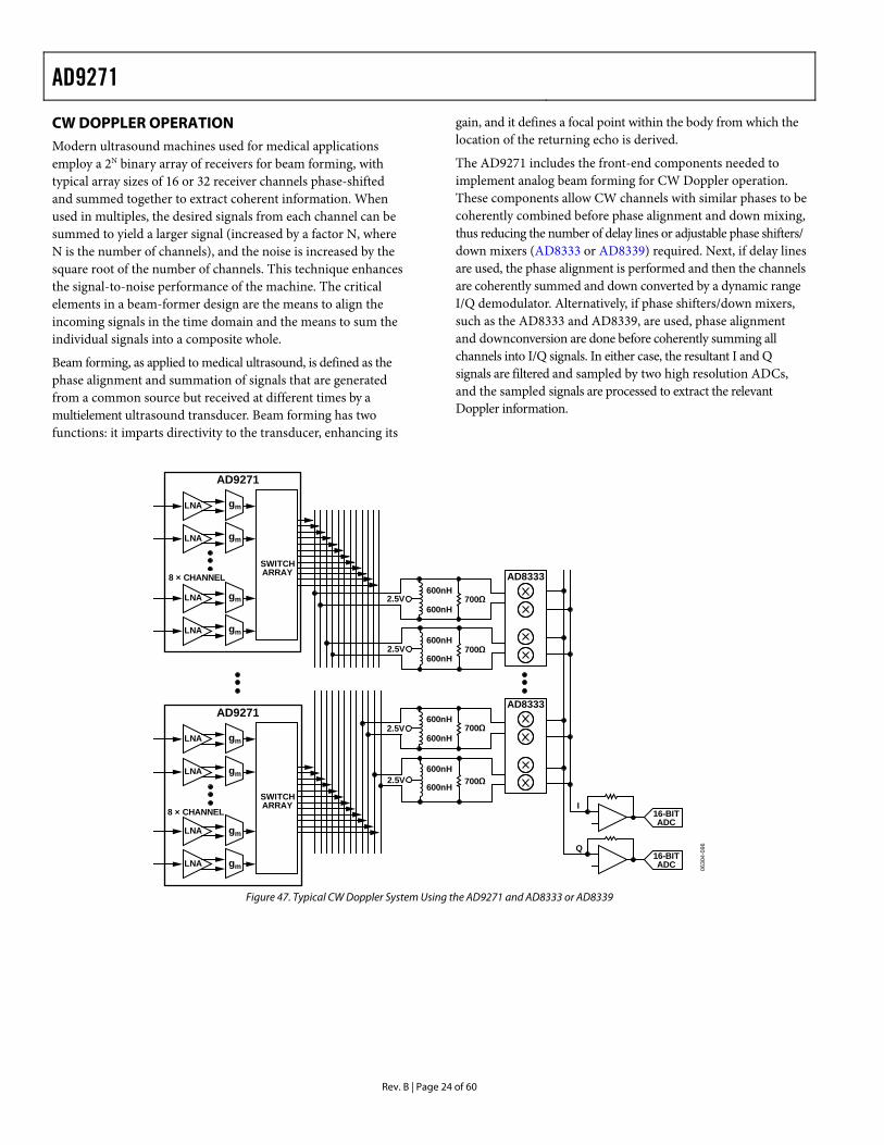
CW DOPPLER OPERATION Modern ultrasound machines used for medical applications employ a 2N binary array of receivers for beam forming, with typical array sizes of 16 or 32 receiver channels phase-shifted and summed together to extract coherent information. When used in multiples, the desired signals from each channel can be summed to yield a larger signal (increased by a factor N, where N is the number of channels), and the noise is increased by the square root of the number of channels. This technique enhances the signal-to-noise performance of the machine. The critical elements in a beam-former design are the means to align the incoming signals in the time domain and the means to sum the individual signals into a composite whole.
Beam forming, as applied to medical ultrasound, is defined as the phase alignment and summation of signals that are generated from a common source but received at different times by a multielement ultrasound transducer. Beam forming has two functions: it imparts directivity to the transducer, enhancing its
gain, and it defines a focal point within the body from which the location of the returning echo is derived.
The AD9271 includes the front-end components needed to implement analog beam forming for CW Doppler operation. These components allow CW channels with similar phases to be coherently combined before phase alignment and down mixing, thus reducing the number of delay lines or adjustable phase shifters/ down mixers (AD8333 or AD8339) required. Next, if delay lines are used, the phase alignment is performed and then the channels are coherently summed and down converted by a dynamic range I/Q demodulator. Alternatively, if phase shifters/down mixers, such as the AD8333 and AD8339, are used, phase alignment and downconversion are done before coherently summing all channels into I/Q signals. In either case, the resultant I and Q signals are filtered and sampled by two high resolution ADCs, and the sampled signals are processed to extract the relevant Doppler information.
AD9271
gm
gm
gm
gm
LNA
Rev. B | Page 24 of 60
gm
gm
gm
gm
SWITCHARRAY
LNA
8 × CHANNEL
16-BITADC
Q
I
LNA
LNA
AD9271
LNA
SWITCHARRAY
8 × CHANNEL
LNA
LNA
LNA
2.5V
AD8333
2.5V
2.5V
2.5V
AD8333
16-BITADC 06
304-
096
600nH
600nH
600nH
600nH
600nH700Ω
700Ω
700Ω
700Ω
600nH
600nH
600nH
Figure 47. Typical CW Doppler System Using the AD9271 and AD8333 or AD8339
AD9271
Rev. B | Page 25 of 60
LNA INPUT-REFERREDNOISE FLOOR
(5.4µV rms) @ AAF BW = 15MHzLNA + VGA NOISE = 1.4nV/ Hz
Crosspoint Switch
Each LNA is followed by a transconductance amp for V/I con-version. Currents can be routed to one of six pairs of differential outputs or to 12 single-ended outputs for summing. Each CWD output pin sinks 2.4 mA dc current, and the signal has a full-scale current of ±2 mA for each channel selected by the crosspoint switch. For example, if four channels were to be summed on one CWD output, the output would sink 9.6 mA dc and have a full-scale current output of ±8 mA. The maximum number of channels combined must be considered when setting the load impedance for I/V conversion to ensure that the full-scale swing and common-mode voltage are within the operating limits of the AD9271. When interfacing to the AD8339, a common-mode voltage of 2.5 V and a full-scale swing of 2.8 V p-p are desired. This can be accomplished by connecting an inductor between each CWD output and a 2.5 V supply, and then connecting either a single-ended or differential load resistance to the CWD± outputs. The value of resistance should be calculated based on the maximum number of channels that can be combined.
CWD± outputs are required under full-scale swing to be greater than 1.5 V and less than CWVDD (3.3 V supply).
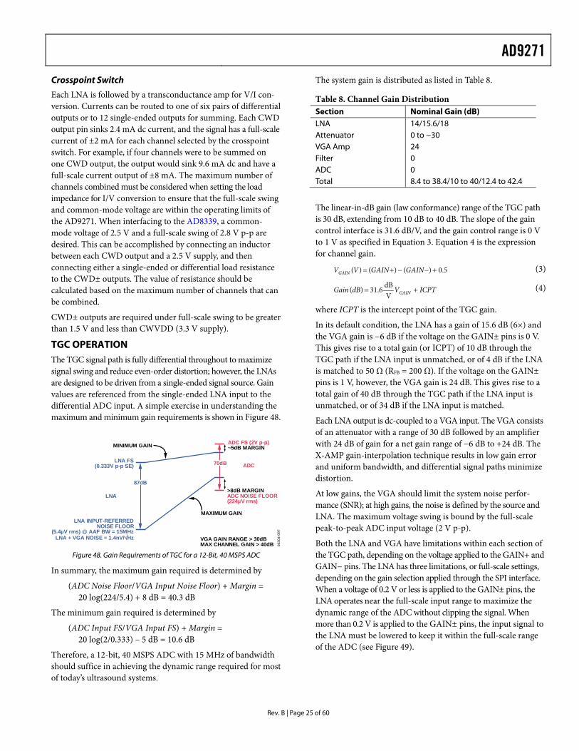
TGC OPERATION The TGC signal path is fully differential throughout to maximize signal swing and reduce even-order distortion; however, the LNAs are designed to be driven from a single-ended signal source. Gain values are referenced from the single-ended LNA input to the differential ADC input. A simple exercise in understanding the maximum and minimum gain requirements is shown in Figure 48.
LNA FS(0.333V p-p SE)
ADC FS (2V p-p)~5dB MARGIN
>8dB MARGINADC NOISE FLOOR(224µV rms)
MINIMUM GAIN
MAXIMUM GAIN
0630
4-09
7
LNA
ADC70dB
87dB
VGA GAIN RANGE > 30dBMAX CHANNEL GAIN > 40dB
Figure 48. Gain Requirements of TGC for a 12-Bit, 40 MSPS ADC
In summary, the maximum gain required is determined by
(ADC Noise Floor/VGA Input Noise Floor) + Margin = 20 log(224/5.4) + 8 dB = 40.3 dB
The minimum gain required is determined by
(ADC Input FS/VGA Input FS) + Margin = 20 log(2/0.333) – 5 dB = 10.6 dB
Therefore, a 12-bit, 40 MSPS ADC with 15 MHz of bandwidth should suffice in achieving the dynamic range required for most of today’s ultrasound systems.
The system gain is distributed as listed in Table 8.
Table 8. Channel Gain Distribution Section Nominal Gain (dB) LNA 14/15.6/18 Attenuator 0 to −30 VGA Amp 24 Filter 0 ADC 0 Total 8.4 to 38.4/10 to 40/12.4 to 42.4
The linear-in-dB gain (law conformance) range of the TGC path is 30 dB, extending from 10 dB to 40 dB. The slope of the gain control interface is 31.6 dB/V, and the gain control range is 0 V to 1 V as specified in Equation 3. Equation 4 is the expression for channel gain.
5.0)()()( +−−+= GAINGAINVVGAIN (3)
ICPTVdBGain GAIN +=VdB6.31)( (4)
where ICPT is the intercept point of the TGC gain.
In its default condition, the LNA has a gain of 15.6 dB (6×) and the VGA gain is −6 dB if the voltage on the GAIN± pins is 0 V. This gives rise to a total gain (or ICPT) of 10 dB through the TGC path if the LNA input is unmatched, or of 4 dB if the LNA is matched to 50 Ω (RFB = 200 Ω). If the voltage on the GAIN± pins is 1 V, however, the VGA gain is 24 dB. This gives rise to a total gain of 40 dB through the TGC path if the LNA input is unmatched, or of 34 dB if the LNA input is matched.
Each LNA output is dc-coupled to a VGA input. The VGA consists of an attenuator with a range of 30 dB followed by an amplifier with 24 dB of gain for a net gain range of −6 dB to +24 dB. The X-AMP gain-interpolation technique results in low gain error and uniform bandwidth, and differential signal paths minimize distortion.
At low gains, the VGA should limit the system noise perfor-mance (SNR); at high gains, the noise is defined by the source and LNA. The maximum voltage swing is bound by the full-scale peak-to-peak ADC input voltage (2 V p-p).
Both the LNA and VGA have limitations within each section of the TGC path, depending on the voltage applied to the GAIN+ and GAIN− pins. The LNA has three limitations, or full-scale settings, depending on the gain selection applied through the SPI interface. When a voltage of 0.2 V or less is applied to the GAIN± pins, the LNA operates near the full-scale input range to maximize the dynamic range of the ADC without clipping the signal. When more than 0.2 V is applied to the GAIN± pins, the input signal to the LNA must be lowered to keep it within the full-scale range of the ADC (see Figure 49).
AD9271
Rev. B | Page 26 of 60
0 0.1 0.2 0.3 0.4 0.5 0.6 0.7 0.8 0.9 1.0
0630
4-1
VGAIN (V)
10
INPU
T FU
LL-S
CA
LE (V
p-p
)
0
0.050
0.100
0.150
0.200
0.250
0.300
0.350
0.400
0.450
LNAGAIN = 6x
LNA GAIN = 8x
LNA GAIN = 5x
Figure 49. LNA/VGA Full-Scale Limitations
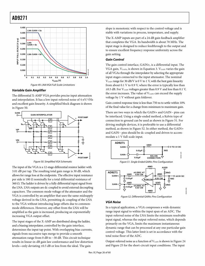
Variable Gain Amplifier
The differential X-AMP VGA provides precise input attenuation and interpolation. It has a low input-referred noise of 4 nV/√Hz and excellent gain linearity. A simplified block diagram is shown in Figure 50.
VIP
GAIN
3dB
VIN
gm
0630
4-07
8
POSTAMP–
POSTAMP+
GAIN INTERPOLATOR
Figure 50. Simplified VGA Schematic
The input of the VGA is a 12-stage differential resistor ladder with 3.01 dB per tap. The resulting total gain range is 30 dB, which allows for range loss at the endpoints. The effective input resistance per side is 180 Ω nominally for a total differential resistance of 360 Ω. The ladder is driven by a fully differential input signal from the LNA. LNA outputs are dc-coupled to avoid external decoupling capacitors. The common-mode voltage of the attenuator and the VGA is controlled by an amplifier that uses the same midsupply voltage derived in the LNA, permitting dc coupling of the LNA to the VGA without introducing large offsets due to common-mode differences. However, any offset from the LNA will be amplified as the gain is increased, producing an exponentially increasing VGA output offset.
The input stages of the X-AMP are distributed along the ladder, and a biasing interpolator, controlled by the gain interface, determines the input tap point. With overlapping bias currents, signals from successive taps merge to provide a smooth attenuation range from 0 dB to −30 dB. This circuit technique results in linear-in-dB gain law conformance and low distortion levels—only deviating ±0.5 dB or less from the ideal. The gain
slope is monotonic with respect to the control voltage and is stable with variations in process, temperature, and supply.
The X-AMP inputs are part of a 24 dB gain feedback amplifier that completes the VGA. Its bandwidth is about 70 MHz. The input stage is designed to reduce feedthrough to the output and to ensure excellent frequency response uniformity across the gain setting.
Gain Control
The gain control interface, GAIN±, is a differential input. The VGA gain, VGAIN, is shown in Equation 3. VGAIN varies the gain of all VGAs through the interpolator by selecting the appropriate input stages connected to the input attenuator. The nominal VGAIN range for 30 dB/V is 0 V to 1 V, with the best gain linearity from about 0.1 V to 0.9 V, where the error is typically less than ±0.5 dB. For VGAIN voltages greater than 0.9 V and less than 0.1 V, the error increases. The value of VGAIN can exceed the supply voltage by 1 V without gain foldover.
Gain control response time is less than 750 ns to settle within 10% of the final value for a change from minimum to maximum gain.
There are two ways in which the GAIN+ and GAIN− pins can be interfaced. Using a single-ended method, a Kelvin type of connection to ground can be used as shown in Figure 51. For driving multiple devices, it is preferable to use a differential method, as shown in Figure 52. In either method, the GAIN+ and GAIN− pins should be dc-coupled and driven to accom-modate a 1 V full-scale input.
AD9271GAIN+
GAIN–
100Ω0 TO 1V DC
50Ω
0.01µF
0.01µF
0630
4-10
9
KELVINCONNECTION
Figure 51. Single-Ended GAIN± Pins Configuration
GAIN–
50ΩGAIN+
AD9271
AVDD
26kΩ
10kΩ
0.01µF
±0.25DC AT0.5V CM
±0.25DC AT0.5V CM
100Ω
499Ω
±0.5V DC
0.01µF
100Ω
499Ω
523Ω
499Ω
0.5V CMAD8138
0630
4-09
8
Figure 52. Differential GAIN± Pins Configuration
VGA Noise
In a typical application, a VGA compresses a wide dynamic range input signal to within the input span of an ADC. The input-referred noise of the LNA limits the minimum resolvable input signal, whereas the output-referred noise, which depends primarily on the VGA, limits the maximum instantaneous dynamic range that can be processed at any one particular gain control voltage. This latter limit is set in accordance with the total noise floor of the ADC.
Output-referred noise as a function of VGAIN is shown in Figure 24 and Figure 25 for the short-circuit input conditions. The input
AD9271
Rev. B | Page 27 of 60
noise voltage is simply equal to the output noise divided by the measured gain at each point in the control range.
The output-referred noise is a flat 63 nV/√Hz over most of the gain range, because it is dominated by the fixed output-referred noise of the VGA. At the high end of the gain control range, the noise of the LNA and source prevail. The input-referred noise reaches its minimum value near the maximum gain control voltage, where the input-referred contribution of the VGA is miniscule.
At lower gains, the input-referred noise and, therefore, the noise figure increases as the gain decreases. The instantaneous dynamic range of the system is not lost, however, because the input capacity increases as the input-referred noise increases. The contribution of the ADC noise floor has the same dependence. The important relationship is the magnitude of the VGA output noise floor relative to that of the ADC.
Gain control noise is a concern in very low noise applications. Thermal noise in the gain control interface can modulate the channel gain. The resultant noise is proportional to the output signal level and is usually evident only when a large signal is present. The gain interface includes an on-chip noise filter, which significantly reduces this effect at frequencies above 5 MHz. Care should be taken to minimize noise impinging at the GAIN± input. An external RC filter can be used to remove VGAIN source noise. The filter bandwidth should be sufficient to accommodate the desired control bandwidth.
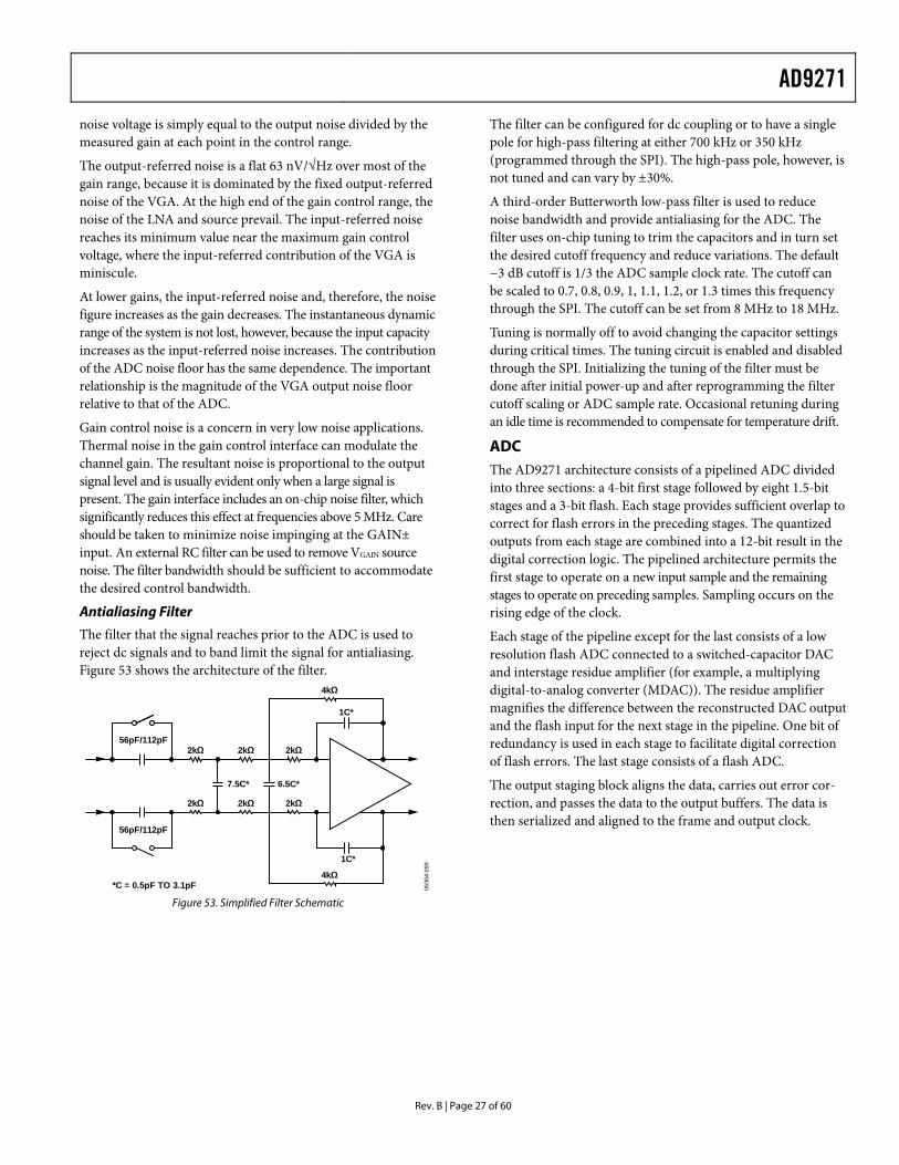
Antialiasing Filter
The filter that the signal reaches prior to the ADC is used to reject dc signals and to band limit the signal for antialiasing. Figure 53 shows the architecture of the filter.
2kΩ 2kΩ 2kΩ
2kΩ 2kΩ 2kΩ
6.5C*7.5C*
1C*
*C = 0.5pF TO 3.1pF
1C*
4kΩ
56pF/112pF
56pF/112pF
4kΩ
0630
4-09
9
Figure 53. Simplified Filter Schematic
The filter can be configured for dc coupling or to have a single pole for high-pass filtering at either 700 kHz or 350 kHz (programmed through the SPI). The high-pass pole, however, is not tuned and can vary by ±30%.
A third-order Butterworth low-pass filter is used to reduce noise bandwidth and provide antialiasing for the ADC. The filter uses on-chip tuning to trim the capacitors and in turn set the desired cutoff frequency and reduce variations. The default −3 dB cutoff is 1/3 the ADC sample clock rate. The cutoff can be scaled to 0.7, 0.8, 0.9, 1, 1.1, 1.2, or 1.3 times this frequency through the SPI. The cutoff can be set from 8 MHz to 18 MHz.
Tuning is normally off to avoid changing the capacitor settings during critical times. The tuning circuit is enabled and disabled through the SPI. Initializing the tuning of the filter must be done after initial power-up and after reprogramming the filter cutoff scaling or ADC sample rate. Occasional retuning during an idle time is recommended to compensate for temperature drift.
ADC The AD9271 architecture consists of a pipelined ADC divided into three sections: a 4-bit first stage followed by eight 1.5-bit stages and a 3-bit flash. Each stage provides sufficient overlap to correct for flash errors in the preceding stages. The quantized outputs from each stage are combined into a 12-bit result in the digital correction logic. The pipelined architecture permits the first stage to operate on a new input sample and the remaining stages to operate on preceding samples. Sampling occurs on the rising edge of the clock.
Each stage of the pipeline except for the last consists of a low resolution flash ADC connected to a switched-capacitor DAC and interstage residue amplifier (for example, a multiplying digital-to-analog converter (MDAC)). The residue amplifier magnifies the difference between the reconstructed DAC output and the flash input for the next stage in the pipeline. One bit of redundancy is used in each stage to facilitate digital correction of flash errors. The last stage consists of a flash ADC.
The output staging block aligns the data, carries out error cor-rection, and passes the data to the output buffers. The data is then serialized and aligned to the frame and output clock.
AD9271
Rev. B | Page 28 of 60
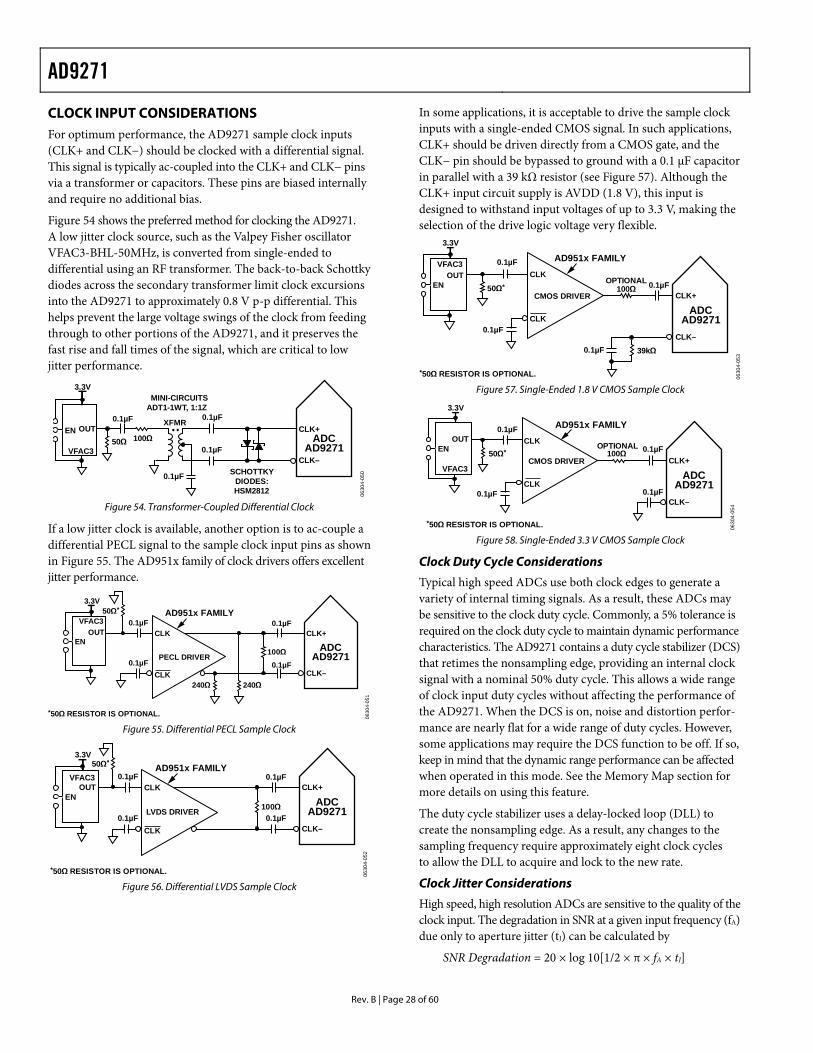
CLOCK INPUT CONSIDERATIONS For optimum performance, the AD9271 sample clock inputs (CLK+ and CLK−) should be clocked with a differential signal. This signal is typically ac-coupled into the CLK+ and CLK− pins via a transformer or capacitors. These pins are biased internally and require no additional bias.
Figure 54 shows the preferred method for clocking the AD9271. A low jitter clock source, such as the Valpey Fisher oscillator VFAC3-BHL-50MHz, is converted from single-ended to differential using an RF transformer. The back-to-back Schottky diodes across the secondary transformer limit clock excursions into the AD9271 to approximately 0.8 V p-p differential. This helps prevent the large voltage swings of the clock from feeding through to other portions of the AD9271, and it preserves the fast rise and fall times of the signal, which are critical to low jitter performance.
0.1µF
0.1µF SCHOTTKYDIODES:HSM2812
0.1µF0.1µF
3.3V
50Ω 100Ω
CLK–
CLK+ADC
AD9271
MINI-CIRCUITSADT1-1WT, 1:1Z
XFMR
0630
4-05
0
VFAC3
OUTEN
Figure 54. Transformer-Coupled Differential Clock
If a low jitter clock is available, another option is to ac-couple a differential PECL signal to the sample clock input pins as shown in Figure 55. The AD951x family of clock drivers offers excellent jitter performance.
100Ω0.1µF
0.1µF0.1µF
0.1µF
240Ω240Ω
AD951x FAMILY50Ω*
CLK
CLK
*50Ω RESISTOR IS OPTIONAL. 0630
4-05
1
CLK–
CLK+
ADCAD9271PECL DRIVER
3.3V
OUTVFAC3
EN
100Ω0.1µF
0.1µF0.1µF
0.1µF
Figure 55. Differential PECL Sample Clock
LVDS DRIVER
CLK
CLK
*50Ω RESISTOR IS OPTIONAL.
CLK–
CLK+
ADCAD9271
0630
4-05
2
AD951x FAMILY3.3V
OUTVFAC3
EN
50Ω*
Figure 56. Differential LVDS Sample Clock
In some applications, it is acceptable to drive the sample clock inputs with a single-ended CMOS signal. In such applications, CLK+ should be driven directly from a CMOS gate, and the CLK− pin should be bypassed to ground with a 0.1 μF capacitor in parallel with a 39 kΩ resistor (see Figure 57). Although the CLK+ input circuit supply is AVDD (1.8 V), this input is designed to withstand input voltages of up to 3.3 V, making the selection of the drive logic voltage very flexible.
0.1µF
0.1µF
0.1µF
39kΩ
CMOS DRIVER50Ω*
OPTIONAL100Ω
0.1µFCLK
CLK
*50Ω RESISTOR IS OPTIONAL.
CLK–
CLK+
ADCAD9271
0630
4-05
3
AD951x FAMILY3.3V
OUTVFAC3
EN
Figure 57. Single-Ended 1.8 V CMOS Sample Clock
0.1µF
0.1µF
0.1µF
CMOS DRIVER50Ω*
OPTIONAL100Ω
CLK
CLK
*50Ω RESISTOR IS OPTIONAL.
0.1µFCLK–
CLK+
ADCAD9271
0630
4-05
4
AD951x FAMILY
3.3V
OUT
VFAC3
EN
Figure 58. Single-Ended 3.3 V CMOS Sample Clock
Clock Duty Cycle Considerations
Typical high speed ADCs use both clock edges to generate a variety of internal timing signals. As a result, these ADCs may be sensitive to the clock duty cycle. Commonly, a 5% tolerance is required on the clock duty cycle to maintain dynamic performance characteristics. The AD9271 contains a duty cycle stabilizer (DCS) that retimes the nonsampling edge, providing an internal clock signal with a nominal 50% duty cycle. This allows a wide range of clock input duty cycles without affecting the performance of the AD9271. When the DCS is on, noise and distortion perfor-mance are nearly flat for a wide range of duty cycles. However, some applications may require the DCS function to be off. If so, keep in mind that the dynamic range performance can be affected when operated in this mode. See the Memory Map section for more details on using this feature.
The duty cycle stabilizer uses a delay-locked loop (DLL) to create the nonsampling edge. As a result, any changes to the sampling frequency require approximately eight clock cycles to allow the DLL to acquire and lock to the new rate.
Clock Jitter Considerations
High speed, high resolution ADCs are sensitive to the quality of the clock input. The degradation in SNR at a given input frequency (fA) due only to aperture jitter (tJ) can be calculated by
SNR Degradation = 20 × log 10[1/2 × π × fA × tJ]
AD9271
Rev. B | Page 29 of 60
In this equation, the rms aperture jitter represents the root mean square of all jitter sources, including the clock input, analog input signal, and ADC aperture jitter. IF undersampling applications are particularly sensitive to jitter (see Figure 59).
The clock input should be treated as an analog signal in cases where aperture jitter may affect the dynamic range of the AD9271. Power supplies for clock drivers should be separated from the ADC output driver supplies to avoid modulating the clock signal with digital noise. Low jitter, crystal-controlled oscillators make the best clock sources, such as the Valpey Fisher VFAC3 series. If the clock is generated from another type of source (by gating, dividing, or other methods), it should be retimed by the original clock during the last step.
Refer to the AN-501 Application Note and the AN-756 Application Note for more in-depth information about how jitter performance relates to ADCs (visit www.analog.com).
1 10 100 1000
16 BITS
14 BITS
12 BITS
50
60
70
80
90
100
110
120
130
0.125ps
0.5ps
10 BITS
8 BITS
30
40 1.0ps2.0ps
ANALOG INPUT FREQUENCY (MHz)
RMS CLOCK JITTER REQUIREMENT
SNR
(dB
)
0630
4-03
8
0.25ps
Figure 59. Ideal SNR vs. Input Frequency and Jitter
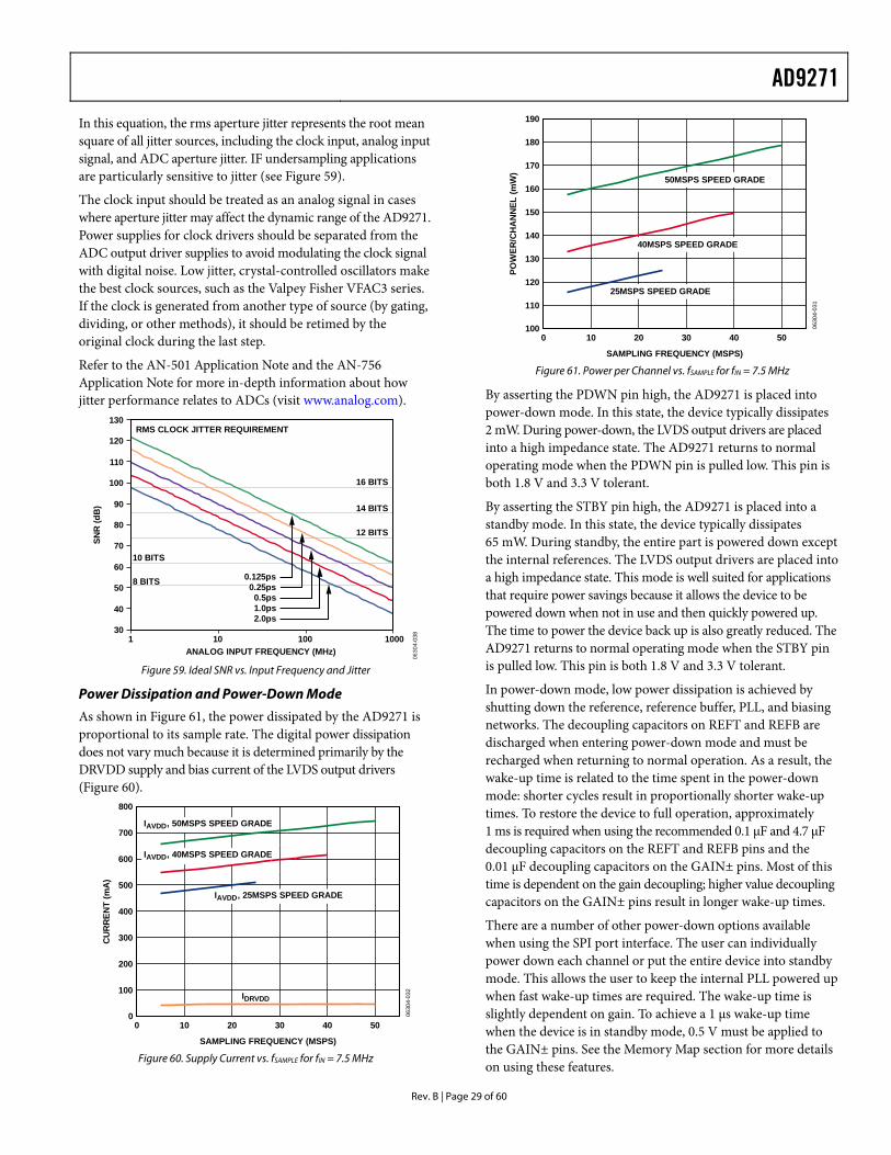
Power Dissipation and Power-Down Mode
As shown in Figure 61, the power dissipated by the AD9271 is proportional to its sample rate. The digital power dissipation does not vary much because it is determined primarily by the DRVDD supply and bias current of the LVDS output drivers (Figure 60).
800
32
CU
RR
ENT
(mA
)
00
0630
4-0
SAMPLING FREQUENCY (MSPS)
700
600
500
400
300
200
100
10 20 30 40 50
IDRVDD
IAVDD, 50MSPS SPEED GRADE
IAVDD, 40MSPS SPEED GRADE
IAVDD, 25MSPS SPEED GRADE
Figure 60. Supply Current vs. fSAMPLE for fIN = 7.5 MHz
190
1000
0630
4-03
1
SAMPLING FREQUENCY (MSPS)
POW
ER/C
HA
NN
EL (m
W)
10 20 30 40 50
180
170
160
150
140
130
120
110
50MSPS SPEED GRADE
40MSPS SPEED GRADE
25MSPS SPEED GRADE
Figure 61. Power per Channel vs. fSAMPLE for fIN = 7.5 MHz
By asserting the PDWN pin high, the AD9271 is placed into power-down mode. In this state, the device typically dissipates 2 mW. During power-down, the LVDS output drivers are placed into a high impedance state. The AD9271 returns to normal operating mode when the PDWN pin is pulled low. This pin is both 1.8 V and 3.3 V tolerant.
By asserting the STBY pin high, the AD9271 is placed into a standby mode. In this state, the device typically dissipates 65 mW. During standby, the entire part is powered down except the internal references. The LVDS output drivers are placed into a high impedance state. This mode is well suited for applications that require power savings because it allows the device to be powered down when not in use and then quickly powered up. The time to power the device back up is also greatly reduced. The AD9271 returns to normal operating mode when the STBY pin is pulled low. This pin is both 1.8 V and 3.3 V tolerant.
In power-down mode, low power dissipation is achieved by shutting down the reference, reference buffer, PLL, and biasing networks. The decoupling capacitors on REFT and REFB are discharged when entering power-down mode and must be recharged when returning to normal operation. As a result, the wake-up time is related to the time spent in the power-down mode: shorter cycles result in proportionally shorter wake-up times. To restore the device to full operation, approximately 1 ms is required when using the recommended 0.1 μF and 4.7 μF decoupling capacitors on the REFT and REFB pins and the 0.01 μF decoupling capacitors on the GAIN± pins. Most of this time is dependent on the gain decoupling; higher value decoupling capacitors on the GAIN± pins result in longer wake-up times.
There are a number of other power-down options available when using the SPI port interface. The user can individually power down each channel or put the entire device into standby mode. This allows the user to keep the internal PLL powered up when fast wake-up times are required. The wake-up time is slightly dependent on gain. To achieve a 1 μs wake-up time when the device is in standby mode, 0.5 V must be applied to the GAIN± pins. See the Memory Map section for more details on using these features.
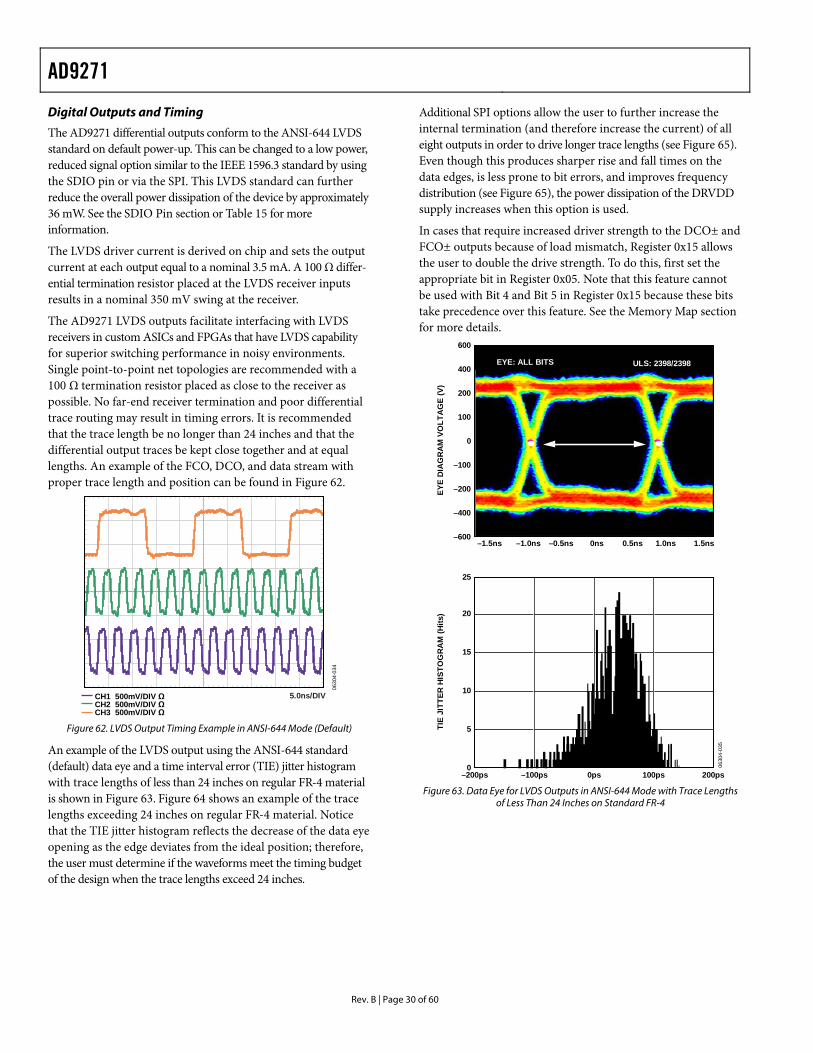
AD9271
Rev. B | Page 30 of 60
0630
4-
CH1 500mV/DIV ΩCH2 500mV/DIV ΩCH3 500mV/DIV Ω
5.0ns/DIV
Digital Outputs and Timing
The AD9271 differential outputs conform to the ANSI-644 LVDS standard on default power-up. This can be changed to a low power, reduced signal option similar to the IEEE 1596.3 standard by using the SDIO pin or via the SPI. This LVDS standard can further reduce the overall power dissipation of the device by approximately 36 mW. See the SDIO Pin section or Table 15 for more information.
The LVDS driver current is derived on chip and sets the output current at each output equal to a nominal 3.5 mA. A 100 Ω differ-ential termination resistor placed at the LVDS receiver inputs results in a nominal 350 mV swing at the receiver.
The AD9271 LVDS outputs facilitate interfacing with LVDS receivers in custom ASICs and FPGAs that have LVDS capability for superior switching performance in noisy environments. Single point-to-point net topologies are recommended with a 100 Ω termination resistor placed as close to the receiver as possible. No far-end receiver termination and poor differential trace routing may result in timing errors. It is recommended that the trace length be no longer than 24 inches and that the differential output traces be kept close together and at equal lengths. An example of the FCO, DCO, and data stream with proper trace length and position can be found in Figure 62.
034
Figure 62. LVDS Output Timing Example in ANSI-644 Mode (Default)
An example of the LVDS output using the ANSI-644 standard (default) data eye and a time interval error (TIE) jitter histogram with trace lengths of less than 24 inches on regular FR-4 material is shown in Figure 63. Figure 64 shows an example of the trace lengths exceeding 24 inches on regular FR-4 material. Notice that the TIE jitter histogram reflects the decrease of the data eye opening as the edge deviates from the ideal position; therefore, the user must determine if the waveforms meet the timing budget of the design when the trace lengths exceed 24 inches.
Additional SPI options allow the user to further increase the internal termination (and therefore increase the current) of all eight outputs in order to drive longer trace lengths (see Figure 65). Even though this produces sharper rise and fall times on the data edges, is less prone to bit errors, and improves frequency distribution (see Figure 65), the power dissipation of the DRVDD supply increases when this option is used.
In cases that require increased driver strength to the DCO± and FCO± outputs because of load mismatch, Register 0x15 allows the user to double the drive strength. To do this, first set the appropriate bit in Register 0x05. Note that this feature cannot be used with Bit 4 and Bit 5 in Register 0x15 because these bits take precedence over this feature. See the Memory Map section for more details.
0630
4-03
5
600
400
–200
200
–100
100
–400
–600
0
–1.5ns –0.5ns–1.0ns 0ns 0.5ns 1.0ns 1.5ns
EYE
DIA
GR
AM
VO
LTA
GE
(V)
EYE: ALL BITS ULS: 2398/2398
25
0
5
10
15
20
–200ps –100ps 0ps 100ps 200ps
TIE
JITT
ER H
ISTO
GR
AM
(Hits
)
Figure 63. Data Eye for LVDS Outputs in ANSI-644 Mode with Trace Lengths
of Less Than 24 Inches on Standard FR-4
AD9271
Rev. B | Page 31 of 60
0630
4-03
6
400
–300
300
–200
200
–100
100
–400
0
–1.5ns –0.5ns–1.0ns 0ns 0.5ns 1.0ns 1.5ns
EYE
DIA
GR
AM
VO
LTA
GE
(V)
EYE: ALL BITS ULS: 2399/2399
25
5
10
15
20
0630
4-03
7
600
–400
400
–200
200
–600
0
–1.5ns –0.5ns–1.0ns 0ns 0.5ns 1.0ns 1.5ns
EYE
DIA
GR
AM
VO
LTA
GE
(V)
EYE: ALL BITS ULS: 2396/2396
25
0
5
10
15
20
–200ps –100ps 0ps 100ps 200p
TIE
JITT
ER H
ISTO
GR
AM
(Hits
)
0–200ps –100ps 0ps 100ps 200p
TIE
JITT
ER H
ISTO
GR
AM
(Hits
)
s Figure 64. Data Eye for LVDS Outputs in ANSI-644 Mode with Trace Lengths
of Greater Than 24 Inches on Standard FR-4
s Figure 65. Data Eye for LVDS Outputs in ANSI-644 Mode with 100 Ω
Termination On and Trace Lengths of Greater Than 24 Inches on Standard FR-4
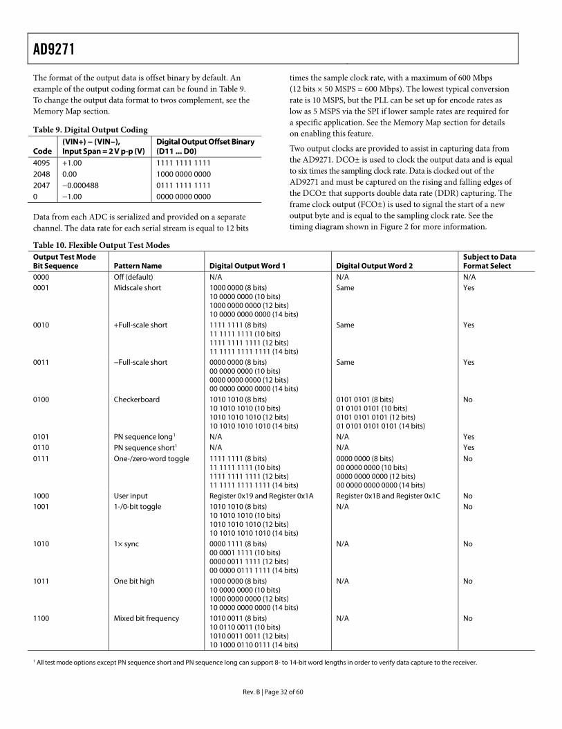
AD9271
Rev. B | Page 32 of 60
The format of the output data is offset binary by default. An example of the output coding format can be found in Table 9. To change the output data format to twos complement, see the Memory Map section.
Table 9. Digital Output Coding
Code (VIN+) − (VIN−), Input Span = 2 V p-p (V)
Digital Output Offset Binary (D11 ... D0)
4095 +1.00 1111 1111 1111 2048 0.00 1000 0000 0000 2047 −0.000488 0111 1111 1111 0 −1.00 0000 0000 0000
Data from each ADC is serialized and provided on a separate channel. The data rate for each serial stream is equal to 12 bits
times the sample clock rate, with a maximum of 600 Mbps (12 bits × 50 MSPS = 600 Mbps). The lowest typical conversion rate is 10 MSPS, but the PLL can be set up for encode rates as low as 5 MSPS via the SPI if lower sample rates are required for a specific application. See the Memory Map section for details on enabling this feature.
Two output clocks are provided to assist in capturing data from the AD9271. DCO± is used to clock the output data and is equal to six times the sampling clock rate. Data is clocked out of the AD9271 and must be captured on the rising and falling edges of the DCO± that supports double data rate (DDR) capturing. The frame clock output (FCO±) is used to signal the start of a new output byte and is equal to the sampling clock rate. See the timing diagram shown in Figure 2 for more information.
Table 10. Flexible Output Test Modes Output Test Mode Bit Sequence Pattern Name Digital Output Word 1 Digital Output Word 2
Subject to Data Format Select
0000 Off (default) N/A N/A N/A 0001 Midscale short 1000 0000 (8 bits)
10 0000 0000 (10 bits) 1000 0000 0000 (12 bits) 10 0000 0000 0000 (14 bits)
Same Yes
0010 +Full-scale short 1111 1111 (8 bits) 11 1111 1111 (10 bits) 1111 1111 1111 (12 bits) 11 1111 1111 1111 (14 bits)
Same Yes
0011 −Full-scale short 0000 0000 (8 bits) 00 0000 0000 (10 bits) 0000 0000 0000 (12 bits) 00 0000 0000 0000 (14 bits)
Same Yes
0100 Checkerboard 1010 1010 (8 bits) 10 1010 1010 (10 bits) 1010 1010 1010 (12 bits) 10 1010 1010 1010 (14 bits)
0101 0101 (8 bits) 01 0101 0101 (10 bits) 0101 0101 0101 (12 bits) 01 0101 0101 0101 (14 bits)
No
0101 PN sequence long1 N/A N/A Yes 0110 PN sequence short1
N/A N/A Yes
0111 One-/zero-word toggle 1111 1111 (8 bits) 11 1111 1111 (10 bits) 1111 1111 1111 (12 bits) 11 1111 1111 1111 (14 bits)
0000 0000 (8 bits) 00 0000 0000 (10 bits) 0000 0000 0000 (12 bits) 00 0000 0000 0000 (14 bits)
No
1000 User input Register 0x19 and Register 0x1A Register 0x1B and Register 0x1C No 1001 1-/0-bit toggle 1010 1010 (8 bits)
10 1010 1010 (10 bits) 1010 1010 1010 (12 bits) 10 1010 1010 1010 (14 bits)
N/A No
1010 1× sync 0000 1111 (8 bits) 00 0001 1111 (10 bits) 0000 0011 1111 (12 bits) 00 0000 0111 1111 (14 bits)
N/A No
1011 One bit high 1000 0000 (8 bits) 10 0000 0000 (10 bits) 1000 0000 0000 (12 bits) 10 0000 0000 0000 (14 bits)
N/A No
1100 Mixed bit frequency 1010 0011 (8 bits) 10 0110 0011 (10 bits) 1010 0011 0011 (12 bits) 10 1000 0110 0111 (14 bits)
N/A No
1 All test mode options except PN sequence short and PN sequence long can support 8- to 14-bit word lengths in order to verify data capture to the receiver.

AD9271
Rev. B | Page 33 of 60
When using the serial port interface (SPI), the DCO± phase can be adjusted in 60° increments relative to the data edge. This enables the user to refine system timing margins if required. The default DCO± timing, as shown in Figure 2, is 90° relative to the output data edge.
An 8-, 10-, and 14-bit serial stream can also be initiated from the SPI. This allows the user to implement different serial streams to test the device’s compatibility with lower and higher resolution systems. When changing the resolution to an 8- or 10-bit serial stream, the data stream is shortened. When using the 14-bit option, the data stream stuffs two 0s at the end of the normal 14-bit serial data.
When using the SPI, all of the data outputs can also be inverted from their nominal state. This is not to be confused with inverting the serial stream to an LSB-first mode. In default mode, as shown in Figure 2, the MSB is represented first in the data output serial stream. However, this can be inverted so that the LSB is repre-sented first in the data output serial stream (see Figure 3).
There are 12 digital output test pattern options available that can be initiated through the SPI. This feature is useful when validating receiver capture and timing. Refer to Table 10 for the output bit sequencing options available. Some test patterns have two serial sequential words and can be alternated in various ways, depending on the test pattern chosen. It should be noted that some patterns may not adhere to the data format select option. In addition, customer user patterns can be assigned in the 0x19, 0x1A, 0x1B, and 0x1C register addresses. All test mode options except PN sequence short and PN sequence long can support 8- to 14-bit word lengths in order to verify data capture to the receiver.
The PN sequence short pattern produces a pseudorandom bit sequence that repeats itself every 29 − 1 bits, or 511 bits. A description of the PN sequence and how it is generated can be found in Section 5.1 of the ITU-T 0.150 (05/96) standard. The only difference is that the starting value is a specific value instead of all 1s (see Table 11 for the initial values).
The PN sequence long pattern produces a pseudorandom bit sequence that repeats itself every 223 − 1 bits, or 8,388,607 bits. A description of the PN sequence and how it is generated can be found in Section 5.6 of the ITU-T 0.150 (05/96) standard. The only differences are that the starting value is a specific value instead of all 1s and the AD9271 inverts the bit stream with relation to the ITU standard (see Table 11 for the initial values).
Table 11. PN Sequence
Sequence Initial Value
First Three Output Samples (MSB First)
PN Sequence Short 0x0df 0xdf9, 0x353, 0x301 PN Sequence Long 0x29b80a 0x591, 0xfd7, 0xa3
Consult the Memory Map section for information on how to change these additional digital output timing features through the SPI.
SDIO Pin
This pin is required to operate the SPI. It has an internal 30 kΩ pull-down resistor that pulls this pin low and is only 1.8 V tolerant. If applications require that this pin be driven from a 3.3 V logic level, insert a 1 kΩ resistor in series with this pin to limit the current.
SCLK Pin
This pin is required to operate the SPI port interface. It has an internal 30 kΩ pull-down resistor that pulls this pin low and is both 1.8 V and 3.3 V tolerant.
CSB Pin
This pin is required to operate the SPI port interface. It has an internal 70 kΩ pull-down resistor that pulls this pin low and is both 1.8 V and 3.3 V tolerant.
RBIAS Pin
To set the internal core bias current of the ADC, place a resistor that is nominally equal to 10.0 kΩ between the RBIAS pin and ground. Using a resistor of another value degrades the performance of the device. Therefore, it is imperative that at least a 1% tolerance on this resistor be used to achieve consistent performance.
Voltage Reference
A stable and accurate 0.5 V voltage reference is built into the AD9271. This is gained up internally by a factor of 2, setting VREF to 1.0 V, which results in a full-scale differential input span of 2.0 V p-p for the ADC. VREF is set internally by default, but the VREF pin can be driven externally with a 1.0 V reference to achieve more accuracy. However, full-scale ranges below 2.0 V p-p are not supported by this device.
When applying the decoupling capacitors to the VREF, REFT, and REFB pins, use ceramic low ESR capacitors. These capacitors should be close to reference pins and on the same layer of the PCB as the AD9271. The recommended capacitor values and configurations for the AD9271 reference pin can be found in Figure 66.
Table 12. Reference Settings
Selected Mode
SENSE Voltage
Resulting VREF (V)
Resulting Differential Span (V p-p)
External Reference
AVDD N/A 2 × external reference
Internal, 2 V p-p FSR
AGND to 0.2 V 1.0 2.0
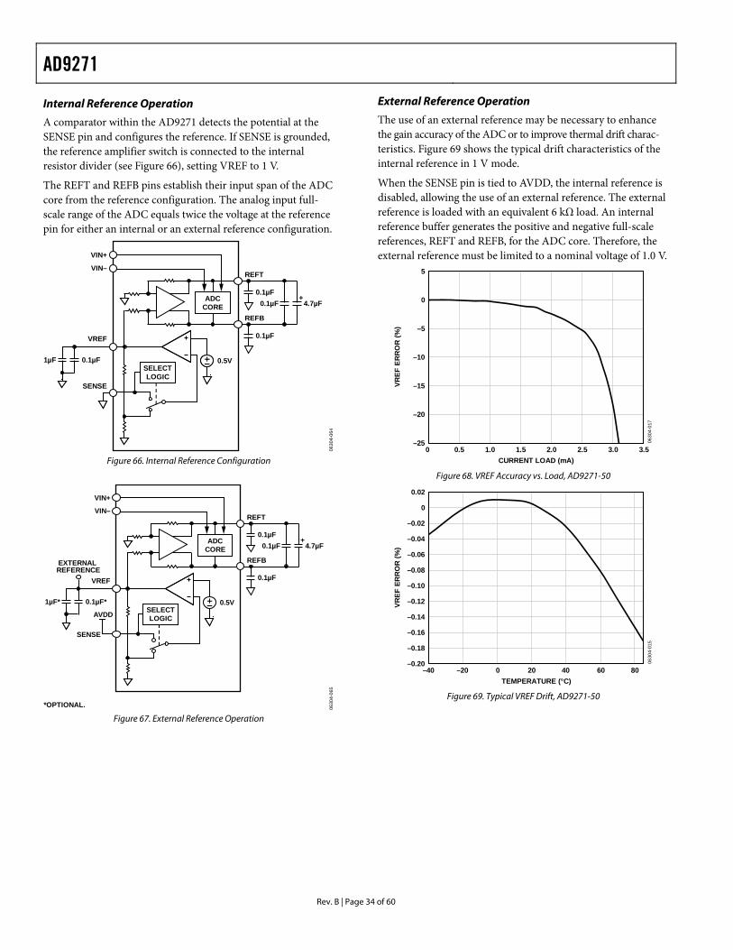
AD9271
Rev. B | Page 34 of 60
External Reference Operation Internal Reference Operation The use of an external reference may be necessary to enhance the gain accuracy of the ADC or to improve thermal drift charac-teristics. Figure 69 shows the typical drift characteristics of the internal reference in 1 V mode.
A comparator within the AD9271 detects the potential at the SENSE pin and configures the reference. If SENSE is grounded, the reference amplifier switch is connected to the internal resistor divider (see Figure 66), setting VREF to 1 V.
When the SENSE pin is tied to AVDD, the internal reference is disabled, allowing the use of an external reference. The external reference is loaded with an equivalent 6 kΩ load. An internal reference buffer generates the positive and negative full-scale references, REFT and REFB, for the ADC core. Therefore, the external reference must be limited to a nominal voltage of 1.0 V.
The REFT and REFB pins establish their input span of the ADC core from the reference configuration. The analog input full-scale range of the ADC equals twice the voltage at the reference pin for either an internal or an external reference configuration.
1µF 0.1µF
VREF
SENSE
0.5V
REFT
0.1µF0.1µF 4.7µF
0.1µF
REFB
SELECTLOGIC
ADCCORE
+
VIN–
VIN+
406
304-
06
6304
-065
.5
5
0
–5
–10
–15
–20
–250 33.02.52.01.51.00.5
0630
4-01
7
VREF
ER
RO
R (%
)
CURRENT LOAD (mA) Figure 66. Internal Reference Configuration Figure 68. VREF Accuracy vs. Load, AD9271-50
0.02
0
–0.02
–0.04
–0.06
–0.08
–0.10
–0.12
–0.14
–0.16
–0.18
–0.20–40 806040200–20
0630
4-01
5
VREF
ER
RO
R (%
)
TEMPERATURE (°C)
VIN–
VIN+
1µF* 0.1µF*
VREF
SENSE
AVDD0.5V
REFT
0.1µF0.1µF 4.7µF
0.1µF
REFB
SELECTLOGIC
ADCCORE
+
EXTERNALREFERENCE
*OPTIONAL.Figure 69. Typical VREF Drift, AD9271-50
0
Figure 67. External Reference Operation
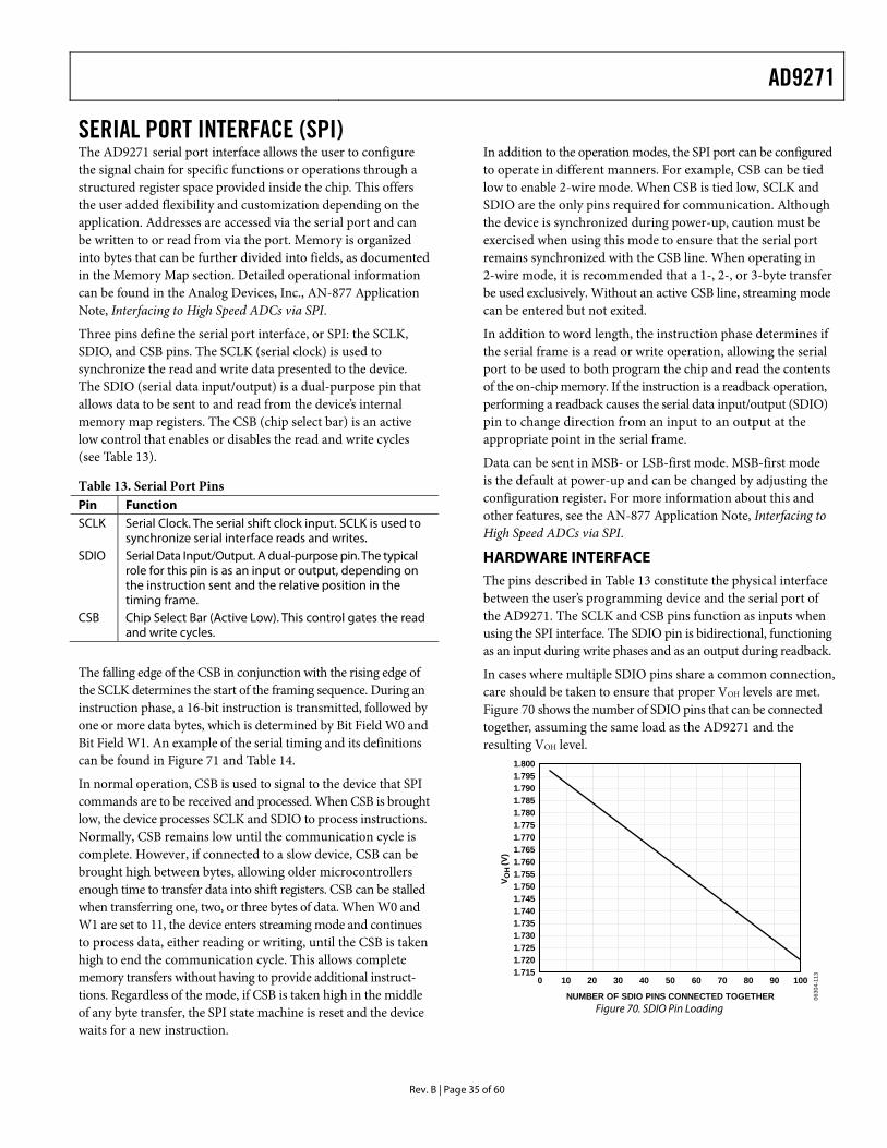
AD9271
Rev. B | Page 35 of 60
SERIAL PORT INTERFACE (SPI) The AD9271 serial port interface allows the user to configure the signal chain for specific functions or operations through a structured register space provided inside the chip. This offers the user added flexibility and customization depending on the application. Addresses are accessed via the serial port and can be written to or read from via the port. Memory is organized into bytes that can be further divided into fields, as documented in the Memory Map section. Detailed operational information can be found in the Analog Devices, Inc., AN-877 Application Note, Interfacing to High Speed ADCs via SPI.
Three pins define the serial port interface, or SPI: the SCLK, SDIO, and CSB pins. The SCLK (serial clock) is used to synchronize the read and write data presented to the device. The SDIO (serial data input/output) is a dual-purpose pin that allows data to be sent to and read from the device’s internal memory map registers. The CSB (chip select bar) is an active low control that enables or disables the read and write cycles (see Table 13).
Table 13. Serial Port Pins Pin Function SCLK Serial Clock. The serial shift clock input. SCLK is used to
synchronize serial interface reads and writes. SDIO Serial Data Input/Output. A dual-purpose pin. The typical
role for this pin is as an input or output, depending on the instruction sent and the relative position in the timing frame.
CSB Chip Select Bar (Active Low). This control gates the read and write cycles.
The falling edge of the CSB in conjunction with the rising edge of the SCLK determines the start of the framing sequence. During an instruction phase, a 16-bit instruction is transmitted, followed by one or more data bytes, which is determined by Bit Field W0 and Bit Field W1. An example of the serial timing and its definitions can be found in Figure 71 and Table 14.
In normal operation, CSB is used to signal to the device that SPI commands are to be received and processed. When CSB is brought low, the device processes SCLK and SDIO to process instructions. Normally, CSB remains low until the communication cycle is complete. However, if connected to a slow device, CSB can be brought high between bytes, allowing older microcontrollers enough time to transfer data into shift registers. CSB can be stalled when transferring one, two, or three bytes of data. When W0 and W1 are set to 11, the device enters streaming mode and continues to process data, either reading or writing, until the CSB is taken high to end the communication cycle. This allows complete memory transfers without having to provide additional instruct-tions. Regardless of the mode, if CSB is taken high in the middle of any byte transfer, the SPI state machine is reset and the device waits for a new instruction.
In addition to the operation modes, the SPI port can be configured to operate in different manners. For example, CSB can be tied low to enable 2-wire mode. When CSB is tied low, SCLK and SDIO are the only pins required for communication. Although the device is synchronized during power-up, caution must be exercised when using this mode to ensure that the serial port remains synchronized with the CSB line. When operating in 2-wire mode, it is recommended that a 1-, 2-, or 3-byte transfer be used exclusively. Without an active CSB line, streaming mode can be entered but not exited.
In addition to word length, the instruction phase determines if the serial frame is a read or write operation, allowing the serial port to be used to both program the chip and read the contents of the on-chip memory. If the instruction is a readback operation, performing a readback causes the serial data input/output (SDIO) pin to change direction from an input to an output at the appropriate point in the serial frame.
Data can be sent in MSB- or LSB-first mode. MSB-first mode is the default at power-up and can be changed by adjusting the configuration register. For more information about this and other features, see the AN-877 Application Note, Interfacing to High Speed ADCs via SPI.
HARDWARE INTERFACE The pins described in Table 13 constitute the physical interface between the user’s programming device and the serial port of the AD9271. The SCLK and CSB pins function as inputs when using the SPI interface. The SDIO pin is bidirectional, functioning as an input during write phases and as an output during readback.
In cases where multiple SDIO pins share a common connection, care should be taken to ensure that proper VOH levels are met. Figure 70 shows the number of SDIO pins that can be connected together, assuming the same load as the AD9271 and the resulting VOH level.
0630
4-11
3
NUMBER OF SDIO PINS CONNECTED TOGETHER
V OH
(V)
1.7151.7201.7251.7301.7351.7401.7451.7501.7551.7601.7651.7701.7751.7801.7851.7901.7951.800
0 302010 40 50 60 70 80 90 100
Figure 70. SDIO Pin Loading
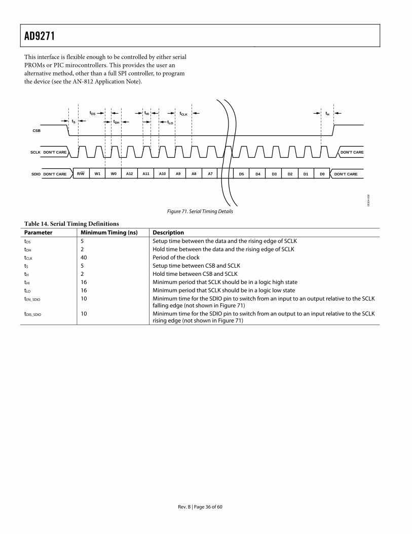
AD9271
Rev. B | Page 36 of 60
This interface is flexible enough to be controlled by either serial PROMs or PIC mirocontrollers. This provides the user an alternative method, other than a full SPI controller, to program the device (see the AN-812 Application Note).
DON’T CARE
DON’T CAREDON’T CARE
DON’T CARE
SDIO
SCLK
CSB
tS tDH
tHI tCLK
tLO
tDS tH
R/W W1 W0 A12 A11 A10 A9 A8 A7 D5 D4 D3 D2 D1 D0
0630
4-06
8
Figure 71. Serial Timing Details
Table 14. Serial Timing Definitions Parameter Minimum Timing (ns) Description tDS 5 Setup time between the data and the rising edge of SCLK tDH 2 Hold time between the data and the rising edge of SCLK tCLK 40 Period of the clock tS 5 Setup time between CSB and SCLK tH 2 Hold time between CSB and SCLK tHI 16 Minimum period that SCLK should be in a logic high state tLO 16 Minimum period that SCLK should be in a logic low state tEN_SDIO 10 Minimum time for the SDIO pin to switch from an input to an output relative to the SCLK
falling edge (not shown in Figure 71) tDIS_SDIO 10 Minimum time for the SDIO pin to switch from an output to an input relative to the SCLK
rising edge (not shown in Figure 71)
AD9271
Rev. B | Page 37 of 60
MEMORY MAP READING THE MEMORY MAP TABLE Each row in the memory map table has eight address locations. The memory map is roughly divided into three sections: the chip configuration register map (Address 0x00 to Address 0x02), the device index and transfer register map (Address 0x04, Address 0x05, and Address 0xFF), and the ADC functions register map (Address 0x08 to Address 0x2D).
The leftmost column of the memory map indicates the register address number; the default value is shown in the second rightmost column. The Bit 7 (MSB) column is the start of the default hexadecimal value given. For example, Address 0x09, the clock register, has a default value of 0x01, meaning that Bit 7 = 0, Bit 6 = 0, Bit 5 = 0, Bit 4 = 0, Bit 3 = 0, Bit 2 = 0, Bit 1 = 0, and Bit 0 = 1, or 0000 0001 in binary. This setting is the default for the duty cycle stabilizer in the on condition. By writing 0 to Bit 0 of this address followed by writing 0x01 in Register 0xFF (transfer bit), the duty cycle stabilizer turns off. It is important to follow each writing sequence with a transfer bit to update the SPI registers. All registers, except Register 0x00, Register 0x02,
Register 0x04, Register 0x05, and Register 0xFF, are buffered with a master-slave latch and require writing to the transfer bit. For more information on this and other functions, consult the AN-877 Application Note, Interfacing to High Speed ADCs via SPI.
RESERVED LOCATIONS Undefined memory locations should not be written to except when writing the default values suggested in this data sheet. Addresses that have values marked as 0 should be considered reserved and have 0 written into their registers during power-up.
DEFAULT VALUES After a reset, critical registers are automatically loaded with default values. These values are indicated in Table 15, where an X refers to an undefined feature.
LOGIC LEVELS An explanation of various registers follows: “Bit is set” is synonymous with “bit is set to Logic 1” or “writing Logic 1 for the bit.” Similarly, “clear a bit” is synonymous with “bit is set to Logic 0” or “writing Logic 0 for the bit.”
AD9271
Rev. B | Page 38 of 60
Table 15. Memory Map Register1 Addr. (Hex) Register Name
Bit 7 (MSB) Bit 6 Bit 5 Bit 4 Bit 3 Bit 2 Bit 1
Bit 0 (LSB)
Default Value
Notes/ Comments
Chip Configuration Registers
00 chip_port_config 0 LSB first 1 = on 0 = off (default)
Soft reset 1 = on 0 = off (default)
1 1 Soft reset 1 = on 0 = off (default)
LSB first 1 = on 0 = off (default)
0 0x18 The nibbles should be mirrored so that LSB- or MSB-first mode is set correctly regardless of shift mode.
01 chip_id Chip ID Bits [7:0] (AD9271 = 0x13), (default)
Read only
Default is unique chip ID, different for each device. This is a read- only register.
02 chip_grade X X Child ID [5:4] (identify device variants of Chip ID) 00 = 50 MSPS (default) 01 = 40 MSPS 10 = 25 MSPS
X X X X 0x00 Child ID used to differentiate graded devices.
Device Index and Transfer Registers
04 device_index_2 X X X X Data Channel H 1 = on (default)0 = off
Data Channel G 1 = on (default)0 = off
Data Channel F 1 = on (default)0 = off
Data Channel E 1 = on (default) 0 = off
0x0F Bits are set to determine which on-chip device receives the next write command.
05 device_index_1 X X Clock Channel DCO± 1 = on 0 = off (default)
Clock Channel FCO± 1 = on 0 = off (default)
Data Channel D 1 = on (default)0 = off
Data Channel C 1 = on (default)0 = off
Data Channel B 1 = on (default)0 = off
Data Channel A 1 = on (default) 0 = off
0x0F Bits are set to determine which on-chip device receives the next write command.
FF device_update X X X X X X X SW transfer 1 = on 0 = off (default)
0x00 Synchronously transfers data from the master shift register to the slave.
ADC Functions Registers
08 modes X X X X LNA bypass 1 = on 0 = off (default)
Internal power-down mode 000 = chip run (default) 001 = full power-down 010 = standby 011 = reset 100 = CW mode (TGC PDWN)
0x00 Determines various generic modes of chip operation.
09 clock X X X X X X X Duty cycle stabilizer 1 = on (default) 0 = off
0x01 Turns the internal duty cycle stabilizer on and off.
AD9271
Rev. B | Page 39 of 60
Addr. (Hex) Register Name
Bit 7 (MSB) Bit 6 Bit 5 Bit 4 Bit 3 Bit 2 Bit 1
Bit 0 (LSB)
Default Value
Notes/ Comments
0D test_io User test mode 00 = off (default) 01 = on, single alternate 10 = on, single once 11 = on, alternate once
Reset PN long gen 1 = on 0 = off (default)
Reset PN short gen 1 = on 0 = off (default)
Output test mode—see Table 10 0000 = off (default) 0001 = midscale short 0010 = +FS short 0011 = −FS short 0100 = checkerboard output 0101 = PN sequence long 0110 = PN sequence short 0111 = one-/zero-word toggle 1000 = user input 1001 = 1-/0-bit toggle 1010 = 1× sync 1011 = one bit high 1100 = mixed bit frequency (format determined by output_mode)
0x00 When this register is set, the test data is placed on the output pins in place of normal data. (Local, expect for PN sequence.)
0F flex_channel_input Filter cutoff frequency control 0000 = 1.3 × 1/3 × fSAMPLE 0001 = 1.2 × 1/3 × fSAMPLE 0010 = 1.1 × 1/3 × fSAMPLE 0011 = 1.0 × 1/3 × fSAMPLE 0100 = 0.9 × 1/3 × fSAMPLE 0101 = 0.8 × 1/3 × fSAMPLE 0110 = 0.7 × 1/3 × fSAMPLE
X X X X 0x30 Antialiasing filter cutoff (global).
10 flex_offset X X 6-bit LNA offset adjustment 011001 = 50 MSPS speed grade 011010 = 40 MSPS speed grade 011111 = 25 MSPS speed grade
0x20 LNA force offset correction (local).
11 flex_gain X X X X X X LNA gain 00 = 5× 01 = 6× 10 = 8×
0x01 LNA gain adjustment (global).
14 output_mode X 0 = LVDS ANSI-644 (default) 1 = LVDS low power, (IEEE 1596.3 similar)
X X X Output invert 1 = on 0 = off (default)
00 = offset binary (default) 01 = twos complement
0x00 Configures the outputs and the format of the data.
15 output_adjust X X Output driver termination 00 = none (default) 01 = 200 Ω 10 = 100 Ω 11 = 100 Ω
X X X DCO± and FCO± 2× drive strength 1 = on 0 = off (default)
0x00 Determines LVDS or other output prop erties. Primarily functions to set the LVDS span and common- mode levels in place of an external resistor.
16 output_phase X X X X 0011 = output clock phase adjust (0000 through 1010) (Default: 180° relative to data edge) 0000 = 0° relative to data edge 0001 = 60° relative to data edge 0010 = 120° relative to data edge 0011 = 180° relative to data edge 0100 = 240° relative to data edge 0101 = 300° relative to data edge 0110 = 360° relative to data edge 0111 = 420° relative to data edge 1000 = 480° relative to data edge 1001 = 540° relative to data edge 1010 = 600° relative to data edge 1011 to 1111 = 660° relative to data edge
0x03 On devices that utilize global clock divide, determines which phase of the divider output is used to supply the output clock. Internal latching is unaffected.
AD9271
Rev. B | Page 40 of 60
Addr. (Hex) Register Name
Bit 7 (MSB) Bit 6 Bit 5 Bit 4 Bit 3 Bit 2 Bit 1
Bit 0 (LSB)
Default Value
Notes/ Comments
19 user_patt1_lsb B7 B6 B5 B4 B3 B2 B1 B0 0x00 User-defined pattern, 1 LSB (global).
1A user_patt1_msb B15 B14 B13 B12 B11 B10 B9 B8 0x00 User-defined pattern, 1 MSB (global).
1B user_patt2_lsb B7 B6 B5 B4 B3 B2 B1 B0 0x00 User-defined pattern, 2 LSB (global).
1C user_patt2_msb B15 B14 B13 B12 B11 B10 B9 B8 0x00 User-defined pattern, 2 MSB (global).
21 serial_control LSB first 1 = on 0 = off (default)
X X X <10 MSPS, low encode rate mode 1 = on 0 = off (default)
000 = 12 bits (default, normal bit stream) 001 = 8 bits 010 = 10 bits 011 = 12 bits 100 = 14 bits
0x00 Serial stream control. Default causes MSB first and the native bit stream (global).
22 serial_ch_stat X X X X X X Channel output reset 1 = on 0 = off (default)
Channel power-down 1 = on 0 = off (default)
0x00 Used to power down individ ual sections of a converter (local).
2B flex_filter X Enable automatic low-pass tuning 1 = on 0 = off (default)
X X X X High-pass filter cutoff 00 = dc (default) 01 = 700 kHz 10 = 350 kHz
0x00 Filter cutoff (global).
2C analog_input X X X X X X X LOSW-x 1 = on 0 = off (default)
0x00 LNA active termination/ input impedance (global).
2D cross_point_switch X X X Crosspoint switch enable 0 0000 = CWD0± (differential) 0 0001 = CWD1± (differential) 0 0010 = CWD2± (differential) 0 0011 = CWD3± (differential) 0 0100 = CWD4± (differential) 0 0101 = CWD5± (differential) 0 0111 = power down CW channel 1 0000 = CWD0+ (single ended) 1 0001 = CWD1+ (single ended) 1 0010 = CWD2+ (single ended) 1 0011 = CWD3+ (single ended) 1 0100 = CWD4+ (single ended) 1 0101 = CWD5+ (single ended) 1 0111 = power down CW channel 1 1000 = CWD0− (single ended) 1 1001 = CWD1− (single ended) 1 1010 = CWD2− (single ended) 1 1011 = CWD3− (single ended) 1 1100 = CWD4− (single ended) 1 1101 = CWD5− (single ended) 1 1111 = power down CW channel
0x07 Crosspoint switch enable (local).
1 X = an undefined feature
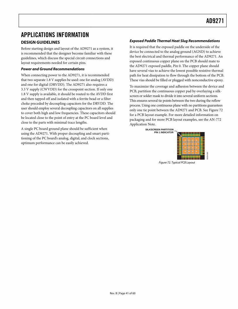
AD9271
Rev. B | Page 41 of 60
APPLICATIONS INFORMATION DESIGN GUIDELINES Before starting design and layout of the AD9271 as a system, it is recommended that the designer become familiar with these guidelines, which discuss the special circuit connections and layout requirements needed for certain pins.
Power and Ground Recommendations
When connecting power to the AD9271, it is recommended that two separate 1.8 V supplies be used: one for analog (AVDD) and one for digital (DRVDD). The AD9271 also requires a 3.3 V supply (CWVDD) for the crosspoint section. If only one 1.8 V supply is available, it should be routed to the AVDD first and then tapped off and isolated with a ferrite bead or a filter choke preceded by decoupling capacitors for the DRVDD. The user should employ several decoupling capacitors on all supplies to cover both high and low frequencies. These capacitors should be located close to the point of entry at the PC board level and close to the parts with minimal trace lengths.
A single PC board ground plane should be sufficient when using the AD9271. With proper decoupling and smart parti-tioning of the PC board’s analog, digital, and clock sections, optimum performance can be easily achieved.
Exposed Paddle Thermal Heat Slug Recommendations
It is required that the exposed paddle on the underside of the device be connected to the analog ground (AGND) to achieve the best electrical and thermal performance of the AD9271. An exposed continuous copper plane on the PCB should mate to the AD9271 exposed paddle, Pin 0. The copper plane should have several vias to achieve the lowest possible resistive thermal path for heat dissipation to flow through the bottom of the PCB. These vias should be filled or plugged with nonconductive epoxy.
To maximize the coverage and adhesion between the device and PCB, partition the continuous copper pad by overlaying a silk-screen or solder mask to divide it into several uniform sections. This ensures several tie points between the two during the reflow process. Using one continuous plane with no partitions guarantees only one tie point between the AD9271 and PCB. See Figure 72 for a PCB layout example. For more detailed information on packaging and for more PCB layout examples, see the AN-772 Application Note.
SILKSCREEN PARTITIONPIN 1 INDICATOR
0630
4-06
9
Figure 72. Typical PCB Layout
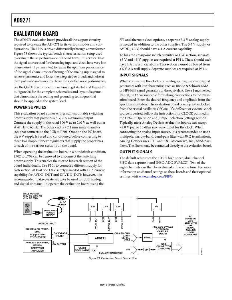
AD9271
Rev. B | Page 42 of 60
EVALUATION BOARD The AD9271 evaluation board provides all the support circuitry required to operate the AD9271 in its various modes and con-figurations. The LNA is driven differentially through a transformer. Figure 73 shows the typical bench characterization setup used to evaluate the ac performance of the AD9271. It is critical that the signal sources used for the analog input and clock have very low phase noise (<1 ps rms jitter) to realize the optimum performance of the signal chain. Proper filtering of the analog input signal to remove harmonics and lower the integrated or broadband noise at the input is also necessary to achieve the specified noise performance.
See the Quick Start Procedure section to get started and Figure 75 to Figure 86 for the complete schematics and layout diagrams that demonstrate the routing and grounding techniques that should be applied at the system level.
POWER SUPPLIES This evaluation board comes with a wall-mountable switching power supply that provides a 6 V, 2 A maximum output. Connect the supply to the rated 100 V ac to 240 V ac wall outlet at 47 Hz to 63 Hz. The other end is a 2.1 mm inner diameter jack that connects to the PCB at P701. Once on the PC board, the 6 V supply is fused and conditioned before connecting to three low dropout linear regulators that supply the proper bias to each of the various sections on the board.
When operating the evaluation board in a nondefault condition, L702 to L704 can be removed to disconnect the switching power supply. This enables the user to bias each section of the board individually. Use P501 to connect a different supply for each section. At least one 1.8 V supply is needed with a 1 A current capability for AVDD_DUT and DRVDD_DUT; however, it is recommended that separate supplies be used for both analog and digital domains. To operate the evaluation board using the
SPI and alternate clock options, a separate 3.3 V analog supply is needed in addition to the other supplies. The 3.3 V supply, or AVDD_3.3 V, should have a 1 A current capability.
To bias the crosspoint switch circuitry or CW section, separate +5 V and −5 V supplies are required at P511. These should each have 1 A current capability. This section cannot be biased from a 6 V, 2 A wall supply. Separate supplies are required at P511.
INPUT SIGNALS When connecting the clock and analog source, use clean signal generators with low phase noise, such as Rohde & Schwarz SMA or HP8644B signal generators or the equivalent. Use a 1 m, shielded, RG-58, 50 Ω coaxial cable for making connections to the evalu-ation board. Enter the desired frequency and amplitude from the specifications tables. The evaluation board is set up to be clocked from the crystal oscillator, OSC401. If a different or external clock source is desired, follow the instructions for CLOCK outlined in the Default Operation and Jumper Selection Settings section. Typically, most Analog Devices evaluation boards can accept ~2.8 V p-p or 13 dBm sine wave input for the clock. When connecting the analog input source, it is recommended to use a multipole, narrow-band, band-pass filter with 50 Ω terminations. Analog Devices uses TTE and K&L Microwave, Inc., band-pass filters. The filter should be connected directly to the evaluation board.
OUTPUT SIGNALS The default setup uses the FIFO5 high speed, dual-channel FIFO data capture board (HSC-ADC-EVALCZ). Two of the eight channels can then be evaluated at the same time. For more information on channel settings on these boards and their optional settings, visit www.analog.com/FIFO.
ROHDE & SCHWARZ,SMA,
2V p-p SIGNALSYNTHESIZER
ROHDE & SCHWARZ,FS5A20
SPECTRUMANALYZER
BAND-PASSFILTER
CH A TO CH H12-BIT
SERIALLVDSAD9271
HSC-ADC-EVALCZFIFO DATACAPTURE
BOARDFPGA
PCRUNNING
ADCANALYZER
ORVISUAL
ANALOGUSER
SOFTWARE
1.8V– +– +
AVD
D_D
UT
VREG
DR
VDD
_DU
T
GN
D
AVD
D_3
.3V
GN
D
GN
D
1.8V
6V DC2A MAX
VFAC3OSCILLATOR
WALL OUTLET100V TO 240V AC47Hz TO 63Hz
SWITCHINGPOWERSUPPLY
– +
GN
D
3.3V– +
PS
SPI SPI
0630
4-07
0
ANALOG INPUT
CW OUTPUT
CLKEVALUATION BOARD
USBCONNECTOR
(DATA/SPI)
Figure 73. Evaluation Board Connection
AD9271
Rev. B | Page 43 of 60
DEFAULT OPERATION AND JUMPER SELECTION SETTINGS The following is a list of the default and optional settings or modes allowed on the AD9271 Rev. B evaluation board.
• Power: Connect the switching power supply that is supplied in the evaluation kit between a rated 100 V ac to 240 V ac wall outlet at 47 Hz to 63 Hz and P701.
• AIN: The evaluation board is set up for a transformer-coupled analog input with an optimum 50 Ω impedance match of 18 MHz of bandwidth. For a different bandwidth response, use the antialiasing filter settings.
• VREF: VREF is set to 1.0 V by tying the SENSE pin to ground, R317. This causes the ADC to operate in 2.0 V p-p full-scale range. A separate external reference option using the ADR510 or ADR520 is also included on the evaluation board. Populate R311 and R315 with 0 Ω resistors and remove C307. Proper use of the VREF options is noted in the Voltage Reference section. Note that ADC full-scale ranges less than 2.0 V p-p are not supported by this device.
• RBIAS: RBIAS has a default setting of 10 kΩ (R301) to ground and is used to set the ADC core bias current. However, note that using other than a 10 kΩ resistor for RBIAS may degrade the performance of the device, depending on the resistor chosen.
• Clock: The default clock input circuitry is derived from a simple transformer-coupled circuit using a high bandwidth 1:1 impedance ratio transformer (T401) that adds a very low amount of jitter to the clock path. The clock input is 50 Ω terminated and ac-coupled to handle single-ended sine wave types of inputs. The transformer converts the single-ended input to a differential signal that is clipped before entering the ADC clock inputs.
The evaluation board is already set up to be clocked from the crystal oscillator, OSC401. This oscillator is a low phase noise oscillator from Valpey Fisher (VFAC3-BHL-50MHz). If a different clock source is desired, remove R403, set Jumper J401 to disable the oscillator from running, and connect the external clock source to the SMA connector, P401.
A differential LVPECL clock driver can also be used to clock the ADC input using the AD9515 (U401). Populate R406 and R407 with 0 Ω resistors and remove R415 and R416 to disconnect the default clock path inputs. In addition, populate C405 and C406 with a 0.1 μF capacitor and remove C409 and C410 to disconnect the default clock path outputs. The AD9515 has many pin-strappable options that are set to a default mode of operation. Consult the AD9515 data sheet for more information about these and other options.
• PDWN: To enable the power-down feature, short P303 to the on position (AVDD) on the PDWN pin.
• STBY: To enable the standby feature, short P302 to the on position (AVDD) on the STBY pin.
• GAIN+, GAIN−: To change the VGA attenuation, drive the GAIN+ pin from 0 V to 1 V on J301. This changes the VGA gain from 0 dB to 30 dB. This feature can also be driven from the R335 and R336 on-board resistive divider by installing a 0 Ω resistor in R337.
• Non-SPI Mode: For users who wish to operate the DUT without using the SPI, remove the jumpers on J501. This disconnects the CSB, SCLK, and SDIO pins from the control bus, allowing the DUT to operate in its simplest mode. Each of these pins has internal termination and will float to its respective level. Note that the device will only work in its default condition.
• CWD+, CWD−: To view the CWD2+/CWD2− and CWD3+/ CWD3− outputs, jumper together the appropriate outputs on P403. All outputs are summed together on IOP and ION buses, fed to a 1:4 impedance ratio transformer, and buffered so that the user can view the output on a spectrum analyzer. This can be configured to be viewed in single-ended mode (default) or in differential mode. To set the voltage for the appropriate number of channels to be summed, change the value of R447 and R448 on the primary transformer (T402).
Upon shipment, the CWD0+/CWD0−, CWD1+/CWD1−, CWD4+/CWD4−, and CWD5+/CWD5− outputs are properly biased and ready to use with the AD8339 quad I/Q demodulator and phase shifter. The AD9271 evaluation board simply snaps into place on the AD8339 evaluation board (AD8339-EVALZ). Remove the jumpers connected to P3A and P4A on the AD8339 evaluation board, and snap the standoffs labeled MH502, MH504, and MH505 that are provided with the AD9271 into the AD8339 evaluation board standoff holes in the center of the board. The standoffs automatically lock into place and create a direct connection between the AD9271 CWDx± outputs and the AD8339 inputs.
• DOUTx+, DOUTx−: If an alternative data capture method to the setup described in Figure 80 is used, optional receiver terminations, R601 to R610, can be installed next to the high speed backplane connector.
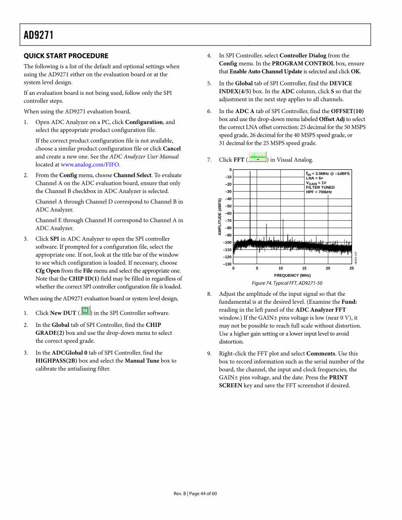
AD9271
Rev. B | Page 44 of 60
4. In SPI Controller, select Controller Dialog from the Config menu. In the PROGRAM CONTROL box, ensure that Enable Auto Channel Update is selected and click OK.
QUICK START PROCEDURE The following is a list of the default and optional settings when using the AD9271 either on the evaluation board or at the system level design. 5. In the Global tab of SPI Controller, find the DEVICE
INDEX(4/5) box. In the ADC column, click S so that the adjustment in the next step applies to all channels.
If an evaluation board is not being used, follow only the SPI controller steps.
6. In the ADC A tab of SPI Controller, find the OFFSET(10) box and use the drop-down menu labeled Offset Adj to select the correct LNA offset correction: 25 decimal for the 50 MSPS speed grade, 26 decimal for the 40 MSPS speed grade, or 31 decimal for the 25 MSPS speed grade.
When using the AD9271 evaluation board,
1. Open ADC Analyzer on a PC, click Configuration, and select the appropriate product configuration file.
If the correct product configuration file is not available, choose a similar product configuration file or click Cancel and create a new one. See the ADC Analyzer User Manual located at www.analog.com/FIFO.
7. Click FFT ( ) in Visual Analog. 0
–1300 2
0630
4-11
9
FREQUENCY (MHz)
AM
PLIT
UD
E (d
BFS
)
5
–10
–20
–30
–40
–50
–60
–70
–80
–90
–100
–110
–120
5 10 15 20
fIN = 3.5MHz @ –1dBFSLNA = 6×VGAIN = 1VFILTER TUNEDHPF = 700kHz
2. From the Config menu, choose Channel Select. To evaluate Channel A on the ADC evaluation board, ensure that only the Channel B checkbox in ADC Analyzer is selected.
Channel A through Channel D correspond to Channel B in ADC Analyzer.
Channel E through Channel H correspond to Channel A in ADC Analyzer.
3. Click SPI in ADC Analyzer to open the SPI controller software. If prompted for a configuration file, select the appropriate one. If not, look at the title bar of the window to see which configuration is loaded. If necessary, choose Cfg Open from the File menu and select the appropriate one. Note that the CHIP ID(1) field may be filled in regardless of whether the correct SPI controller configuration file is loaded. Figure 74. Typical FFT, AD9271-50
8. Adjust the amplitude of the input signal so that the fundamental is at the desired level. (Examine the Fund: reading in the left panel of the ADC Analyzer FFT window.) If the GAIN± pins voltage is low (near 0 V), it may not be possible to reach full scale without distortion. Use a higher gain setting or a lower input level to avoid distortion.
When using the AD9271 evaluation board or system level design,
1. Click New DUT ( ) in the SPI Controller software.
2. In the Global tab of SPI Controller, find the CHIP GRADE(2) box and use the drop-down menu to select the correct speed grade.
3. In the ADCGlobal 0 tab of SPI Controller, find the HIGHPASS(2B) box and select the Manual Tune box to calibrate the antialiasing filter.
9. Right-click the FFT plot and select Comments. Use this box to record information such as the serial number of the board, the channel, the input and clock frequencies, the GAIN± pins voltage, and the date. Press the PRINT SCREEN key and save the FFT screenshot if desired.
AD9271
Rev. B | Page 45 of 60
06304-086
SCHEMATICS AND ARTWORK
AIN
CHB
AIN
CHA
AIN
CHC
AIN
CH
D
6
14 2
5 3T1
04
AD
T1-1
WT
+
3524
1
6
AD
T1-1
WT
+
T10
2
3524
1
6
AD
T1-1
WT
+
T10
36
14 2
5 3T1
01
AD
T1-1
WT
+
R12
20-D
NP
0-D
NP
R11
3R15
00-D
NP
R10
40-D
NP
CT
DCT
C
CT
BCTA
R16
049.9
C11
5
0.1
UF
0.1
UF
C12
4
R12
10
C10
6
22PF
0.1
UF-
DN
P
C10
8
22PF
C10
2C10
4
0.1
UF-
DN
P
C12
0
0.1
UF-
DN
P
0.1
UF-
DN
P
C11
9
C11
8
0.1
UF-D
NP
0.1
UF-
DN
P
C11
7
GN
DD
GN
DA
J10
1
R12
849.9
-DN
P
49.9
-DN
PR11
9
49.9
-DN
PR11
0
R10
149.9
-DN
P
LG
A
LIA
LOSW
A
LO-A
0
R10
5
R10
8
200
R10
7
1K-D
NP
C10
3
0.1
UF
0-D
NP
R15
4
0-D
NP
R10
9R10
60
0R13
0
R10
2
0
R14
90
AVD
D
10K-D
NP
R14
2
R14
110
K-D
NP
49.9
R15
8CT
A
0R13
7
R13
2
00.1
UF
C12
1
C10
1
0.1
UF
0.1
UF
C10
5
C12
2
0.1
UF
0
R16
2
R11
20
GN
DB
J10
2
CT
BR15
949.9
10K
-DN
PR14
3
R14
410K
-DN
P
AVD
D
0R13
8
0
R11
1
R15
10
0R11
5R11
80-D
NP
R15
5
0-D
NP
0.1
UF
C10
7
1K-D
NP
R11
6
200
R11
7
R11
4
0
LO-B
LOSW
B
LIB
LGB
LGD
LID
LOSW
D
LO-D
0
R12
3
R13
5
200
R13
4
1K-D
NP
0-D
NP
R15
7
0-D
NP
R13
6R13
30
0R15
3
R12
9
0
R14
00
AVD
D
10K-D
NP
R14
8
R14
710
K-D
NP
49.9
R16
1CT
D
J10
4
0R13
1
R16
4
0
C11
3
0.1
UF
0.1
UF
C10
9
C12
3
0.1
UF
0
R16
3
GN
DC
J10
3
CT
C
10K
-DN
PR14
5
R14
610K
-DN
P
AVD
D
0R13
9
0
R10
3
R15
20
0R12
4R12
70-D
NP
R15
6
0-D
NP
0.1
UF
C11
1
1K-D
NP
R12
5
200
R12
6
R12
0
0
LO-C
LOSW
C
LIC
LGC
C11
2
0.1
UF-
DN
P22PF
C11
0
C11
4
22PF
0.1
UF-
DN
P
C11
6
Figure 75. Evaluation Board Schematic, DUT Analog Input Circuits
AD9271
Rev. B | Page 46 of 60
06304-087
AIN
CH
E
AIN
CHF
0-D
NP
R22
2
R21
20-D
NP
J20
1
49
R2
R2
0
J20
2
0R2
AIN
CHG
AIN
CHH
3 52 4
1
6
AD
T1-1
WT
+
T20
46
142
53T2
02
AD
T1-1
WT
+
6
142
53T20
3
AD
T1-1
WT
+
3 52 4
1
6
AD
T1-1
WT
+
T20
1
0-D
NP
R24
1
R23
10-D
NP
CT
HCT
G
CT
FCT
E49.9
-DN
PR21
9
R20
8
200
C21
0
22PF
C21
6
0.1U
F-D
NP
22PF
C21
4
0.1
UF-
DN
P
C21
2
22PF
C20
6C20
8
0.1U
F-D
NP
0.1U
F-D
NP
C22
0
C21
9
0.1
UF-
DN
P
0.1U
F-D
NP
C21
8
C21
7
0.1
UF-
DN
P
R24
210
K-D
NP
0-D
NP
R25
4
C20
1
0.1
UF
R20
149.9
-DN
P
.9-D
NP
10
R22
849.9
-DN
P
GN
DH
CTHCT
G
GN
DG
GN
DF
CT
FCT
E
GN
DE
LGE
LIE
LOSW
E
LO-E
0
R20
5
R20
7
1K-D
NP
C20
3
0.1
UF
0-D
NP
R20
9R20
60
0R24
9
R20
2
0
R20
30
AVD
D
10K-D
NP
R24
3
49.9
R25
8
0R22
1
R23
2
00.1
UF
C22
1
0.1
UF
C20
5
C22
2
0.1
UF
0
R26
2
30
R25
949.9
10K-D
NP
R20
4
R24
410
K-D
NP
AVD
D3
8
0
R21
1
R25
00
0R21
5R21
80-
DN
P
R25
5
0-D
NP
0.1
UF
C20
7
1K-D
NP
R21
6
200
R21
7
R21
4
0
LO-F
LOSW
F
LIF
LGF
LGH
LIH
LOSW
H
LO-H
0
R22
3
R23
5
200
R23
4
1K-D
NP
C21
5
0.1
UF
0-D
NP
R25
7
0-D
NP
R23
6R23
30
0R25
2
R22
9
0
R24
00
AVD
D
10K-D
NP
R24
8
R24
710
K-D
NP
49.9
R26
1
J20
4
0R25
3
R26
4
00.1
UF
C22
4
C21
3
0.1
UF
0.1
UF
C20
9
C22
3
0.1
UF
0
R26
3
R23
70
J20
3
R26
049.9
10K-D
NP
R24
5
R24
610
K-D
NP
AVD
D
0R23
9
0
R21
3
R25
10
0R22
4R22
70-D
NP
R25
6
0-D
NP
0.1
UF
C21
1
1K-D
NP
R22
5
200
R22
6
R22
0
0
LO-G
LOSW
G
LIG
LGG
C20
2
22PF
0.1U
F-D
NP
C20
4
Figure 76. Evaluation Board Schematic, DUT Analog Input Circuits (Continued)
AD9271
Rev. B | Page 47 of 60
06304-088
CW
CW
V-
V+TRIM/NC
AD
9271BSVZ-5
0
CLK
+
CLK
-CSB
CWD0+
CWD0-
CWD1+
CWD1-
CWD2+
CWD2-
CWD3+
CWD3-
CWD4+
CWD4-
CWD5+
CWD5-
CWVDD DOUTC+
DOUTD+
DOUTF+
DOUTG+
DOUTH+
DOUTC-
DOUTD-
DOUTF-
DOUTG-
DOUTH-
DCO+
DCO-
DOUTA+
DOUTA-
DOUTB+
DOUTB-
DOUTE+
DOUTE-
DRVDD
FCO+
FCO-
GAIN+
GAIN-
LGA
LGB
LGC
LGD
LGE
LGF
LGG
LGH
LIA
LIB
LIC
LID
LIE
LIF
LIG
LIH
LO-A
LO-B
LO-C
LO-D
LO-E
LO-F
LO-G
LO-H
LOSWA
LOSWB
LOSWC
LOSWD
LOSWE
LOSWF
LOSWG
LOSWH
PAD
PDWN
RAVDD
RBIAS
REFB
REFT
SCLK
SD
IO
SENSE
STDBY
VREF
AVDD
AVDD
AVDD
AVDD
AVDD
AVDD
AVDD
AVDD
AVDD
AVDD
DRVDD
AVDD
AVDD
AVDD
AVDD
AVDD
AVDD
AVDD
AVDD
GAIN
DRIV
EIN
PUT
Vref Selec t
Vref=0.5V(1+R313/R312)
Vref = External
Vref=1V
Remove C307 when
using external Vref
Ref
eren
ceCircu
itry
26
54606672 55616773 53
79
78
81
80
83
82
94
93
96
95
98
97
84
46
44
42
40
34
32
30
28
45
43
41
39
33
31
29
27
36
35
47
50
38
37
86
85
56626874 57636975 596571
77
99
586470
76
49
92
91
88
87
5152
90
48
89
100
1012
13
U302
ADR510ARTZ
8.0
6KR335
R3251K
21
P30
3
1KR309
R337
0-D
NP
C301
0.1UF
C305
0.1
UF
VREF_
DUT
470KR308
4.7UF
C302
0.1
UFC308
R338
10K
1K R326
R302
49.9
R3040
0 R331
GG
ND
R319
1K
0.1UFC303C304
0.1UF
C309
0.1
UF
1 2P30
2
VSEN
SE_D
UT
R313DNP
AVDD
R317
0
DNPR312
R311
0-DNP
AVDD
10KR310
R336
10K
R303
100
SCLK
_D
UT
CSB_D
UT
J301
AVDD
AVDD
R301
10K
AVDD
IN
DRVDD_DUT
LOSWE
AVDD_3.3V
LOSWD
AVDD
LO-D
CWD0-
CWD1+
CWD1-
CWD0+
CWD2+
CWD2-
VSENSE_DUT
VREF_DUT
CWD5+
LO-E
CWD4-
CWD4+
CWD5-
CWD3+
CWD3-
AVDD
10 16 2243 9 15 21 2423 252 8 14 201 7 13 195 11 176 12 18
U301
LGF
CLKLIE
LGE
LIF
LOSWF
LO-F
LIG
LGG
LO-G
LOSWG
CLKLIH
LGH
LOSWH
LO-H
AVDD
AVDD
AVDD
AVDD
AVDD
CHH
CHH
CHF
CHG
CHG
DCO
DCO
FCO
CHE
CHE
CHF
CHB
CHA
CHA
DRVDD_DUT
CHC
CHC
CHB
CHD
CHD
FCO
AVDD
LGA
LO-A
LIA
LOSWA
LO-B
LGC
LIB
LOSWB
LGB
LGD
LID
LO-C
LIC
LOSWC
SD
IO_D
UT
AVDD
AVDD
AVDD
R315
0-DNP
0-DNP
R316
0.1
UF
C306
1UF
C307
Figure 77. Evaluation Board Schematic, DUT, VREF, and Gain Circuitry
AD9271
Rev. B | Page 48 of 60
06304-089
CLK
CLK
B
GND
GN
D_P
AD
OUT0
OUT0
B
OUT1
OUT1
B
RSET
S0
S1
S10
S2
S3
S4
S5
S6
S7
S8
S9
SYN
CB VREF
VSSIG
NAL=
DN
C;2
7,28
SIG
NAL=
AVD
D_3
.3V;4
,17,
20,2
1,24
,26,
29,3
0
+IN
1
+IN
2
-IN
1
-IN
2
OUT1
OUT2
V+
V-
AD
822A
RTZ+-
+-
GN
DTC
OU
VCTR
I-
STAT
E
AO
UT
OPT
ION
AL
CO
NN
ECTIO
N
TO
AD
8339
EVAL
BO
AR
D
AO
UT
OPTIO
NAL
CLO
CK
DRIV
ECIR
CU
IT
LVD
SO
UTPU
T
CLI
PSIN
EO
UT
(DEFA
ULT)
LVPECLO
UTPUT
AD
9515Pin
-str
apse
ttin
gs
WD
OPP
LER
CIR
CU
ITR
Y
ENABLE
DIS
ABLE
C
EN
C
EN
C
4 3
VFA
C3
43
612
5
T402
AD
TT4-
1T+
1 2
H-L
-50M
HZ
OSC40
1
3
5
2
6
1
78
4
U40
2
3
2
1
CR40
1H
SM
S-2
812
2 3
31
33
23
22
19
18
32
25
16
7
15
14
13
12
11
10
9
8
5
6
1
U40
1
AD
9515B
CPZ
1 2
L408
560U
H
21
560U
H
L407
21
560U
H
L406
1 2
L405
560U
H
2 1
560U
H
L402
12
L401
560U
H
2 1
560U
H
L403
12
L404
560U
H
127
R44
8
R44
712
7
AVD
D_3
.3V
R43
6
0
R42
4
0-D
NP
0R42
5
R42
7
0
0-D
NP
R43
2
0-D
NP
R42
6
R45
2
0
0R46
6
0-D
NP
R40
6
R40
210
K
C409
0.1UF
0
R41
7
6
142
53T4
01
AD
T1-1
W+
750
R45
4
R42
2
100
S0
C40
1
0.1U
F
OPT
_CLK
OPT
_CLK
0.1U
F
C41
1
R41
5
0
100
R42
3
240
R42
1R42
024
0
C42
1
0.1U
F
0.1U
F
C41
9C42
0
0.1U
F
0.1U
F
C42
2
R41
149
.9-D
NP
2 4 6 8
AVD
D_3
.3V
CLK
S10
S9
S8
S7
S6
S5S
4
S3
S2
S1
AVD
D_3
.3V
AVD
D_3
.3V
AVD
D_3
.3V
AVD
D_3
.3V
AVD
D_3
.3V
AVD
D_3
.3V
DN
PR41
2
AVD
D_3
.3V
10K
R41
0D
NP
R40
8R40
9D
NP
OPT
_CLK
R40
7
0-D
NP
R44
6
0
0-D
NP
R45
9
49.9
R40
4
R41
44.
12K
AVD
D_3
.3V
0.1U
F-D
NP
C40
8
C40
7
0.1U
F-D
NP
C40
6
0.1U
F-D
NP
0.1U
F-D
NP
C40
5
7531P4
03
CLK
S10
1
E402
0R40
3
CLK
R41
8
0
R41
6
0
C402
0.1UF
J402
R45
549
.9
R45
00
AVD
D_3
.3V
10K
R40
1
1
2
3
J401
CW
D5-
CW
D5+
CW
D4-
CW
D4+
CW
D1-
CW
D1+
CW
D0-
CW
D0+
24687 5 3 1
P405
AVD
D_2
.5V
+5V
R45
3
750
-5V
CW
D2
CW
D1
0
R45
1
R44
90-
DN
P
R46
20
0R46
0
CW
D1
AVDD_3.3V
CW
D2-
CW
D2+
0-D
NP
R46
5
49.9
R45
8
J403
CW
D2
R46
10-
DN
P
R46
30
0R46
4R46
7
750
750
R46
8
AVD
D_2
.5V
AVD
D_2
.5V
R46
9
750
750
R47
0
AVD
D_2
.5V
13578 6 4 2
P406
R40
50
0.1UF
C403
0.1UF
C410
1
E401
S9
S8
S7
S6
S5
S4
S3
S2
S1
S0
P402
AVD
D_3
.3V
ION
IOP
CW
D3-
CW
D3+
P401
CLK
R41
310
K
OPT
_CLK
AVD
D_3
.3V
AVD
D_3
.3V
AVD
D_3
.3V
AVD
D_3
.3V
C41
4
0.1U
F0.
1UF
C41
2C41
3
0.1U
F0.
1UF
C41
6C41
5
0.1U
F0.
1UF
C41
7C41
8
0.1U
F
R42
8
0-D
NP
R43
0
0-D
NP
R43
4
0-D
NP
R42
9
0 0R43
1
0R43
3
R43
5
0
0R43
9
R44
1
0 0R44
3
R44
5
0
0-D
NP
R43
7
R43
8
0-D
NP
0-D
NP
R44
0
R44
2
0-D
NP
0-D
NP
R44
4
Figure 78. Evaluation Board Schematic, Clock and CW Doppler Circuitry
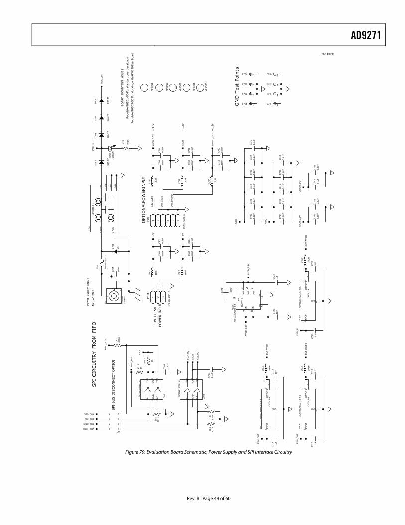
AD9271
Rev. B | Page 49 of 60
06304-090
7.5VP
OW
ER
2.5M
MJAC
K
2A
Y1 VCC
Y2A2
GN
D
A1
Y1
VCC
Y2A2
GN
D
A1
SD
GN
DOU
TIN
NR
INO
UT
OU
TAD
P333
5
BIA
S
PSG
CB
CG CG
CG
GND
OUTP
UT
1O
UTP
UT
4IN
PUT
GND
OUTP
UT
1O
UTP
UT
4IN
PUT
GND
INPU
TO
UTP
UT
1O
UTP
UT
4
+1.8
v
6V,
2A
ma
x
Popula
teM
H501-5
04f
ors
tandar
dboar
dev
aluat
ion
+1.8
v
Pow
erSupply
Inpu
t
GN
DTest
Poi
nts
BO
ARD
MO
UN
TIN
GH
OLE
S
Popula
teM
H503-5
05f
ord
ock
ingw
ith
AD
8339Eva
lBoar
d
SPI
BU
S D
ISCO
NN
ECT
OPT
ION
POW
ER I
NPU
TCW
+/-
5V
SPI
CIR
CU
ITRY
FRO
MFI
FO
OPT
ION
ALP
OW
ERIN
PUT
+3.3
vM
H501
MH
502
MH
503
MH
504
MH
505
4
23
1
AD
P333
9AKCZ-3
.3-R
LU
705
1
32
4
AD
P333
9AKCZ-1
.8-R
L
1
32
4
AD
P333
9AKCZ-1
.8-R
L
21D
705
S2A
-TP
12
D70
4
S2A
-TP2
1D70
3
S2A
-TP
12
D70
2
S2A
-TP
1 3
2 4 5 6
L70
1
BN
X01
6-0
1
F70
1
NAN
OSM
DC
110
F
1 2 3 4 5 6P501
Z5.
531.
3625
.0
AVD
D_2
.5V
64
7
18
3 2
5U
706
AD
P333
5ACPZ
-2.5
1 2 3P511
Z5.
531.
3325
.0
1 2 3456
NC7W
Z16
P6X_N
L
U70
3
6 5 4321
U70
2
NC7W
Z07
P6X_N
L
C70
4
10U
F
C50
1
10U
F
C71
7
1UF
C71
0
0.1U
F
CR70
2G
REE
N
240
R71
6
C72
1
100P
F
C50
4
0.1U
F
0.1U
F
C50
2
2 1
D70
1
C70
3
0.1U
F
10U
F
C71
1
C70
7
10U
F
10U
F
C70
9
10U
F
C50
3
1K
R71
0
R71
110
K
1
2
3
P70
1
1E704
DU
T_AVD
D1
2
L70
5
10U
H
1UF
C71
5
21
10U
H
L50
1
1UF
C72
2C72
3
1UF
AVD
D
AVD
D
0.1U
F
C73
0
C71
2
0.1U
F
1E701
DUT_
DRVD
D
DU
T_AVD
D
3.3V
_AVD
D
-5V
+5V
0.1U
F
C70
2
CSB_D
UT
AVD
D
SCLK
_DU
T
6
8 7
5
AVD
D
SD
IO_D
UT
AVD
D_3
.3V
1K
R71
2
R71
3
1K
PWR_O
UT
PWR_I
N
SDI_CHA
SDO_CHA
12
L50
2
10U
H
12
L70
3
10U
HAVD
D_3
.3V
21
10U
H
L70
2
AVD
D
0.1U
F
C70
8
12
L70
4
10U
HD
RVD
D_D
UT
1E702
1E703 1E707
1E706
1E708
1E705
C73
1
0.1U
F0.
1UF
C73
3C73
2
0.1U
F
C73
5
0.1U
F0.
1UF
C73
4
C74
8
0.1U
F0.
1UF
C74
6C74
7
0.1U
F0.
1UF
C74
5C74
4
0.1U
F
0.1U
F
C74
0
0.1U
F
C75
1
AVD
D_3
.3V
DRVD
D_D
UT
C74
3
0.1U
F
C74
2
0.1U
F
AVD
D_3
.3V
21
10U
H
L70
6
DUT_
DRVD
D
PWR_I
N
C71
9
1UF
1UF
C72
0
12
L70
7
10U
H3.
3V_A
VD
D
R71
510
K
U70
4
U70
7
10K
R71
4
C71
4
1UFPW
R_O
UT
2
4 3
1
J501CSB1_CHA
SCLK_CHA
1UF
C71
6PWR_O
UT
Figure 79. Evaluation Board Schematic, Power Supply and SPI Interface Circuitry
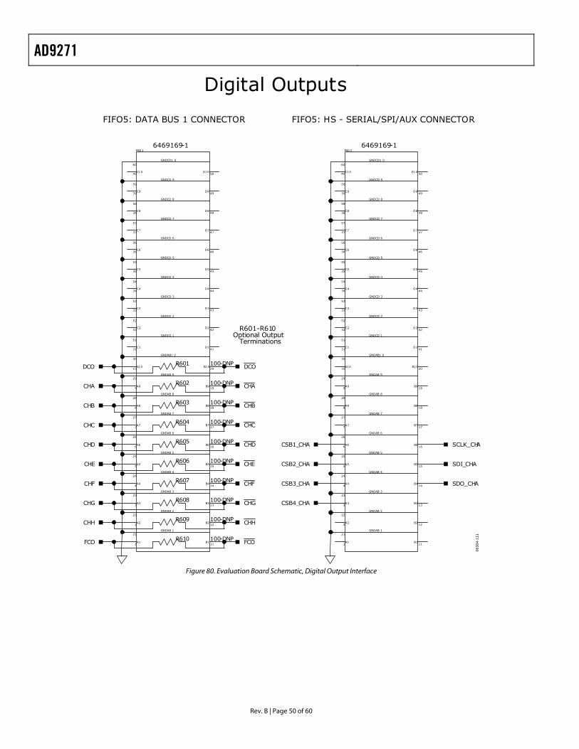
AD9271
Rev. B | Page 50 of 60
0630
4-11
1
Digital Outputs
A1 B1
GNDAB 1
A10
A2
A3
A4
A5
A6
A7
A8
A9
B10
B2
B3
B4
B5
B6
B7
B8
B9
C1
C10
C2
C3
C4
C5
C6
C7
C8
C9
D1
D10
D2
D3
D4
D5
D6
D7
D8
D9
GNDAB1 0
GNDAB 2
GNDAB 3
GNDAB 4
GNDAB 5
GNDAB 6
GNDAB 7
GNDAB 8
GNDAB 9
GNDCD 1
GNDCD1 0
GNDCD 2
GNDCD 3
GNDCD 4
GNDCD 5
GNDCD 6
GNDCD 7
GNDCD 8
GNDCD 9
A1 B1
GNDAB 1
A10
A2
A3
A4
A5
A6
A7
A8
A9
B10
B2
B3
B4
B5
B6
B7
B8
B9
C1
C10
C2
C3
C4
C5
C6
C7
C8
C9
D1
D10
D2
D3
D4
D5
D6
D7
D8
D9
GNDAB1 0
GNDAB 2
GNDAB 3
GNDAB 4
GNDAB 5
GNDAB 6
GNDAB 7
GNDAB 8
GNDAB 9
GNDCD 1
GNDCD1 0
GNDCD 2
GNDCD 3
GNDCD 4
GNDCD 5
GNDCD 6
GNDCD 7
GNDCD 8
GNDCD 9
Optional OutputTerminations
R601-R610
FIFO5: DATA BUS 1 CONNECTOR FIFO5: HS - SERIAL/SPI/AUX CONNECTOR
10
2
3
4
5
6
7
8
9
20
12
13
14
15
16
17
18
19
31
40
32
33
34
35
36
37
38
39
41
50
42
43
44
45
46
47
48
49
30
22
23
24
25
26
27
28
29
51
60
52
53
54
55
56
57
58
59
P60 16469169-1
59
58
57
56
55
54
53
52
60
51
29
28
27
26
25
24
23
22
30
49
48
47
46
45
44
43
42
50
41
39
38
37
36
35
34
33
32
40
31
19
18
17
16
15
14
13
12
20
9
8
7
6
5
4
3
2
10
P60 26469169-1
100-DNPR609
R608 100-DNP
100-DNPR607
R606 100-DNP
100-DNPR605
R604 100-DNP
100-DNPR603
R602 100-DNP
R601 100-DNP
CHH
SDI_CHA
SCLK_CH
1 11
21 21
111
R610 100-DNP
ACSB1_CHA
DCO
CHD
CHG
CHF
CHE
CHC
CHB
CHA
DCO
FCO
CHA
CHB
CHC
CHD
CHE
CHF
CHG
CHH
CSB2_CHA
CSB3_CHA
CSB4_CHA
SDO_CHA
FCO
Figure 80. Evaluation Board Schematic, Digital Output Interface
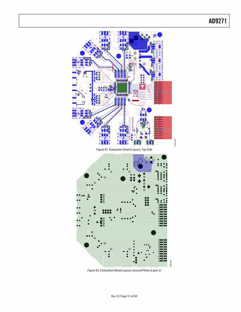
AD9271
Rev. B | Page 51 of 60
0630
4-08
4
Figure 81. Evaluation Board Layout, Top Side
0630
4-08
3
Figure 82. Evaluation Board Layout, Ground Plane (Layer 2)
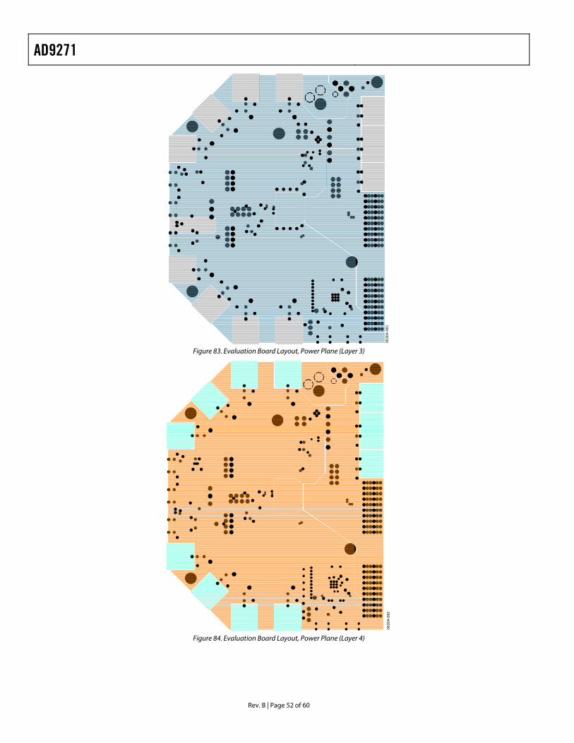
AD9271
Rev. B | Page 52 of 60
0630
4-08
1
Figure 83. Evaluation Board Layout, Power Plane (Layer 3)
0630
4-08
2
Figure 84. Evaluation Board Layout, Power Plane (Layer 4)
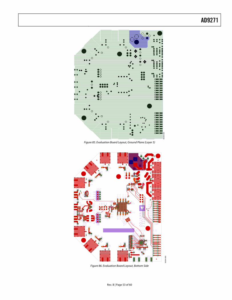
AD9271
Rev. B | Page 53 of 60
4-08
006
30
Figure 85. Evaluation Board Layout, Ground Plane (Layer 5)
0630
4-08
5
Figure 86. Evaluation Board Layout, Bottom Side
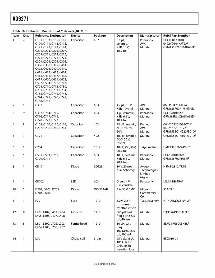
AD9271
Rev. B | Page 54 of 60
Table 16. Evaluation Board Bill of Materials (BOM)1 Item Qty. Reference Designator Device Package Description Manufacturer RoHS Part Number 1 70 C101, C103, C105, C107,
C109, C111, C113, C115, C121, C122, C123, C124, C201, C203, C205, C207, C209, C211, C213, C215, C221, C222, C223, C224, C301, C303, C304, C305, C306, C308, C309, C401, C402, C403, C409, C410, C411, C412, C413, C414, C415, C416, C417, C418, C419, C420, C421, C422, C502, C504, C702, C703, C708, C710, C712, C730, C731, C732, C733, C734, C735, C740, C742, C743, C744, C745, C746, C747, C748, C751
Capacitor 402 0.1 μF, ceramic, X5R, 10 V, 10% tol
Panasonic AVX Murata
ECJ-0EB1A104K2 0402YD104KAT2A2 GRM155R71C104KA88D2
2 1 C302 Capacitor 603 4.7 μF, 6.3 V, X5R, 10% tol
AVX Murata
06036D475KAT2A GRM188R60J475KE19D
3 9 C307, C714, C715, C716, C717, C719, C720, C722, C723
Capacitor 603 1 μF, ceramic, X5R, 6.3 V, 10% tol
Panasonic Murata
ECJ-1VB0J105K2 GRM188R61C105KA93D2
4 8 C102, C106, C110, C114, C202, C206, C210, C214
Capacitor 402 22 pF, ceramic, NPO, 5% tol, 50 V
Kemet AVX Murata
C0402C220J5GACTU2 04025A220JAT2A2 GRM1555C1H220JZ01D2
5 1 C721 Capacitor 402 100 pF, ceramic, COG, 50 V, 5% tol
Murata GRM1555C1H101JZ01D2
6 1 C704 Capacitor 1812 10 μF, X5S, 50 V, 20% tol
Taiyo Yuden UMK432C106MM-T2
7 5 C501, C503, C707, C709, C711
Capacitor 603 10 μF, ceramic, X5R, 6.3 V, 20% tol
Panasonic Murata
ECJ-1VB0J106M2 GRM188R60J106M2
8 1 CR401 Diode SOT23 30 V, 20 mA, dual Schottky
Avago Technologies Limited (Agilent)
HSMS-2812-TR1G
9 1 CR702 LED 603 Green, 4 V, 5 m candela
Panasonic LNJ314G8TRA2
10 5 D701, D702, D703, D704, D705
Diode DO-214AB 3 A, 30 V, SMC Micro Commercial Co.
S2A-TP2
11 1 F701 Fuse 1210 6.0 V, 2.2 A trip current resettable fuse
Tyco/Raychem NANOSMDC110F-22
12 8 L401, L402, L403, L404, L405, L406, L407, L408
Inductor 1210 560 μH, test freq 1 kHz, 5% tol, 40 mA
Murata LQH32MN561J23L2
13 8 L501, L502, L702, L703, L704, L705, L706, L707
Ferrite bead 1210 10 μH, test freq 100 MHz, 25% tol, 500 mA
Murata BLM31PG500SH1L2
14 1 L701 Choke coil 5-pin 25 V dc, 15 A, 100 kHz to 1 GHz, 40 dB insertion loss
Murata BNX016-01
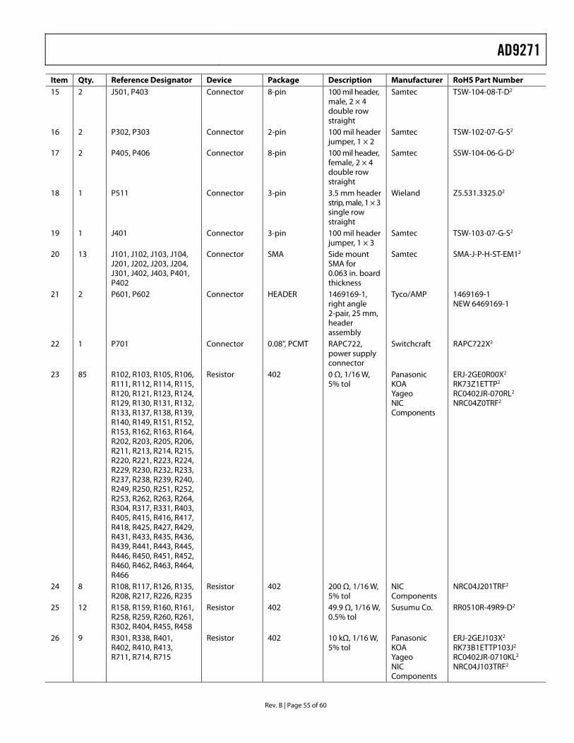
AD9271
Rev. B | Page 55 of 60
Item Qty. Reference Designator Device Package Description Manufacturer RoHS Part Number 15 2 J501, P403 Connector 8-pin 100 mil header,
male, 2 × 4 double row straight
Samtec TSW-104-08-T-D2
16 2 P302, P303 Connector 2-pin 100 mil header jumper, 1 × 2
Samtec TSW-102-07-G-S2
17 2 P405, P406 Connector 8-pin 100 mil header, female, 2 × 4 double row straight
Samtec SSW-104-06-G-D2
18 1 P511 Connector 3-pin 3.5 mm header strip, male, 1 × 3 single row straight
Wieland Z5.531.3325.02
19 1 J401 Connector 3-pin 100 mil header jumper, 1 × 3
Samtec TSW-103-07-G-S2
20 13 J101, J102, J103, J104, J201, J202, J203, J204, J301, J402, J403, P401, P402
Connector SMA Side mount SMA for 0.063 in. board thickness
Samtec SMA-J-P-H-ST-EM12
21 2 P601, P602 Connector HEADER 1469169-1, right angle 2-pair, 25 mm, header assembly
Tyco/AMP 1469169-1 NEW 6469169-1
22 1 P701 Connector 0.08", PCMT RAPC722, power supply connector
Switchcraft RAPC722X2
23 85 R102, R103, R105, R106, R111, R112, R114, R115, R120, R121, R123, R124, R129, R130, R131, R132, R133, R137, R138, R139, R140, R149, R151, R152, R153, R162, R163, R164, R202, R203, R205, R206, R211, R213, R214, R215, R220, R221, R223, R224, R229, R230, R232, R233, R237, R238, R239, R240, R249, R250, R251, R252, R253, R262, R263, R264, R304, R317, R331, R403, R405, R415, R416, R417, R418, R425, R427, R429, R431, R433, R435, R436, R439, R441, R443, R445, R446, R450, R451, R452, R460, R462, R463, R464, R466
Resistor 402 0 Ω, 1/16 W, 5% tol
Panasonic KOA Yageo NIC Components
ERJ-2GE0R00X2 RK73Z1ETTP2 RC0402JR-070RL2 NRC04Z0TRF2
24 8 R108, R117, R126, R135, R208, R217, R226, R235
Resistor 402 200 Ω, 1/16 W, 5% tol
NIC Components
NRC04J201TRF2
25 12 R158, R159, R160, R161, R258, R259, R260, R261, R302, R404, R455, R458
Resistor 402 49.9 Ω, 1/16 W, 0.5% tol
Susumu Co. RR0510R-49R9-D2
26 9 R301, R338, R401, R402, R410, R413, R711, R714, R715
Resistor 402 10 kΩ, 1/16 W, 5% tol
Panasonic KOA Yageo NIC Components
ERJ-2GEJ103X2 RK73B1ETTP103J2 RC0402JR-0710KL2 NRC04J103TRF2
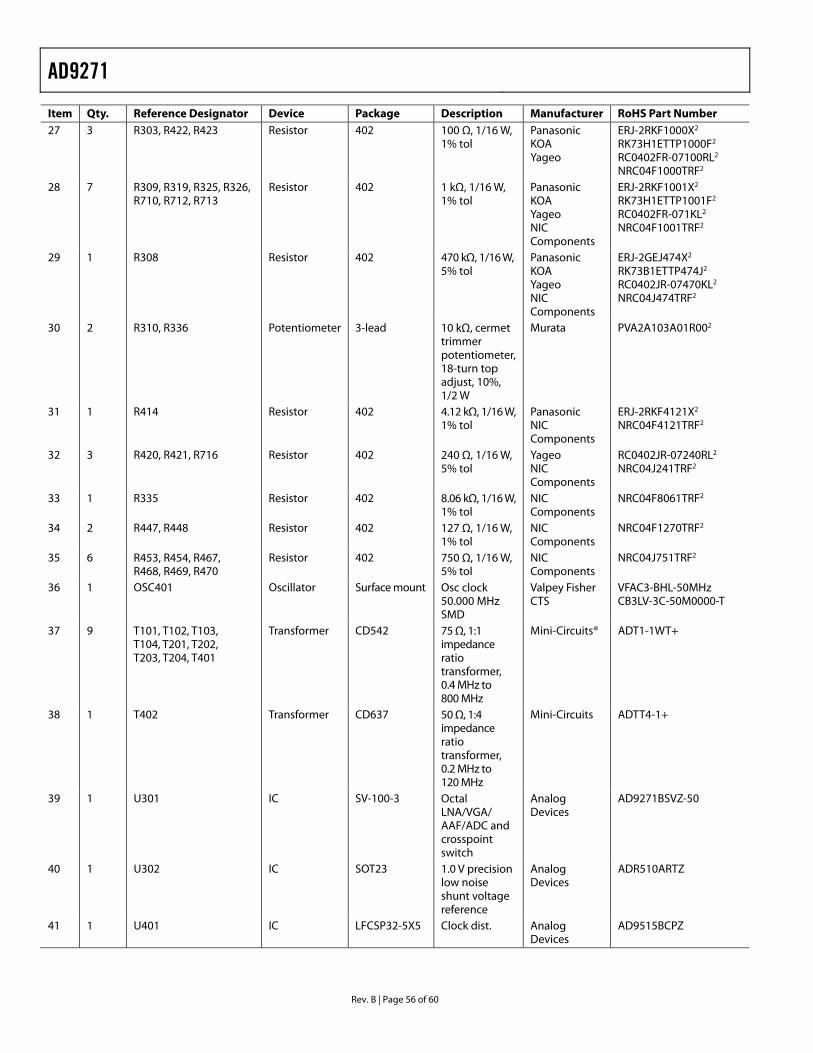
AD9271
Rev. B | Page 56 of 60
Item Qty. Reference Designator Device Package Description Manufacturer RoHS Part Number 27 3 R303, R422, R423 Resistor 402 100 Ω, 1/16 W,
1% tol Panasonic KOA Yageo
ERJ-2RKF1000X2 RK73H1ETTP1000F2 RC0402FR-07100RL2 NRC04F1000TRF2
28 7 R309, R319, R325, R326, R710, R712, R713
Resistor 402 1 kΩ, 1/16 W, 1% tol
Panasonic KOA Yageo NIC Components
ERJ-2RKF1001X2 RK73H1ETTP1001F2 RC0402FR-071KL2 NRC04F1001TRF2
29 1 R308 Resistor 402 470 kΩ, 1/16 W, 5% tol
Panasonic KOA Yageo NIC Components
ERJ-2GEJ474X2 RK73B1ETTP474J2 RC0402JR-07470KL2 NRC04J474TRF2
30 2 R310, R336 Potentiometer 3-lead 10 kΩ, cermet trimmer potentiometer, 18-turn top adjust, 10%, 1/2 W
Murata PVA2A103A01R002
31 1 R414 Resistor 402 4.12 kΩ, 1/16 W, 1% tol
Panasonic NIC Components
ERJ-2RKF4121X2 NRC04F4121TRF2
32 3 R420, R421, R716 Resistor 402 240 Ω, 1/16 W, 5% tol
Yageo NIC Components
RC0402JR-07240RL2 NRC04J241TRF2
33 1 R335 Resistor 402 8.06 kΩ, 1/16 W, 1% tol
NIC Components
NRC04F8061TRF2
34 2 R447, R448 Resistor 402 127 Ω, 1/16 W, 1% tol
NIC Components
NRC04F1270TRF2
35 6 R453, R454, R467, R468, R469, R470
Resistor 402 750 Ω, 1/16 W, 5% tol
NIC Components
NRC04J751TRF2
36 1 OSC401 Oscillator Surface mount Osc clock 50.000 MHz SMD
Valpey Fisher CTS
VFAC3-BHL-50MHz CB3LV-3C-50M0000-T
37 9 T101, T102, T103, T104, T201, T202, T203, T204, T401
Transformer CD542 75 Ω, 1:1 impedance ratio transformer, 0.4 MHz to 800 MHz
Mini-Circuits® ADT1-1WT+
38 1 T402 Transformer CD637 50 Ω, 1:4 impedance ratio transformer, 0.2 MHz to 120 MHz
Mini-Circuits ADTT4-1+
39 1 U301 IC SV-100-3 Octal LNA/VGA/ AAF/ADC and crosspoint switch
Analog Devices
AD9271BSVZ-50
40 1 U302 IC SOT23 1.0 V precision low noise shunt voltage reference
Analog Devices
ADR510ARTZ
41 1 U401 IC LFCSP32-5X5 Clock dist. Analog Devices
AD9515BCPZ
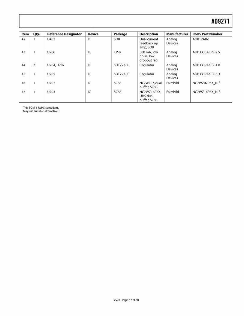
AD9271
Rev. B | Page 57 of 60
Item Qty. Reference Designator Device Package Description Manufacturer RoHS Part Number 42 1 U402 IC SO8 Dual current
feedback op amp, SO8
Analog Devices
AD812ARZ
43 1 U706 IC CP-8 500 mA, low noise, low dropout reg
Analog Devices
ADP3335ACPZ-2.5
44 2 U704, U707 IC SOT223-2 Regulator Analog Devices
ADP3339AKCZ-1.8
45 1 U705 IC SOT223-2 Regulator Analog Devices
ADP3339AKCZ-3.3
46 1 U702 IC SC88 NC7WZ07, dual buffer, SC88
Fairchild NC7WZ07P6X_NL2
47 1 U703 IC SC88 NC7WZ16P6X, UHS dual buffer, SC88
Fairchild NC7WZ16P6X_NL2
1 This BOM is RoHS compliant. 2 May use suitable alternative.
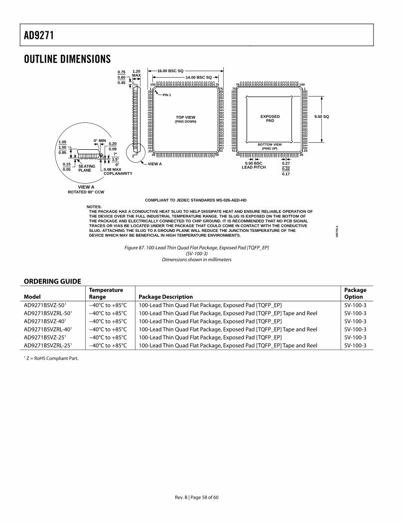
AD9271
Rev. B | Page 58 of 60
COMPLIANT TO JEDEC STANDARDS MS-026-AED-HD
0.270.220.17
OUTLINE DIMENSIONS
1
2526 50
7610075
51
14.00 BSC SQ16.00 BSC SQ
0.50 BSCLEAD PITCH
0.750.600.45
1.20MAX
1
252650
76 10075
51
PIN 1
9.50 SQTOP VIEW(PINS DOWN)
BOTTOM VIEW(PINS UP)
1.051.000.95
0.200.09
0.08 MAXCOPLANARITY
0° MIN
7°3.5°
0°
VIEW AROTATED 90° CCW
SEATINGPLANE
0.150.05
VIEW A
EXPOSEDPAD
NOTES:THE PACKAGE HAS A CONDUCTIVE HEAT SLUG TO HELP DISSIPATE HEAT AND ENSURE RELIABLE OPERATION OFTHE DEVICE OVER THE FULL INDUSTRIAL TEMPERATURE RANGE. THE SLUG IS EXPOSED ON THE BOTTOM OFTHE PACKAGE AND ELECTRICALLY CONNECTED TO CHIP GROUND. IT IS RECOMMENDED THAT NO PCB SIGNALTRACES OR VIAS BE LOCATED UNDER THE PACKAGE THAT COULD COME IN CONTACT WITH THE CONDUCTIVESLUG. ATTACHING THE SLUG TO A GROUND PLANE WILL REDUCE THE JUNCTION TEMPERATURE OF THEDEVICE WHICH MAY BE BENEFICIAL IN HIGH TEMPERATURE ENVIRONMENTS. 08
0706
-A
Figure 87. 100-Lead Thin Quad Flat Package, Exposed Pad [TQFP_EP]
(SV-100-3) Dimensions shown in millimeters
ORDERING GUIDE
Model Temperature Range Package Description
Package Option
AD9271BSVZ-501 −40°C to +85°C 100-Lead Thin Quad Flat Package, Exposed Pad [TQFP_EP] SV-100-3
AD9271BSVZRL-501 −40°C to +85°C 100-Lead Thin Quad Flat Package, Exposed Pad [TQFP_EP] Tape and Reel SV-100-3
AD9271BSVZ-401 −40°C to +85°C 100-Lead Thin Quad Flat Package, Exposed Pad [TQFP_EP] SV-100-3
AD9271BSVZRL-401 −40°C to +85°C 100-Lead Thin Quad Flat Package, Exposed Pad [TQFP_EP] Tape and Reel SV-100-3
AD9271BSVZ-251 −40°C to +85°C 100-Lead Thin Quad Flat Package, Exposed Pad [TQFP_EP] SV-100-3
AD9271BSVZRL-251 −40°C to +85°C 100-Lead Thin Quad Flat Package, Exposed Pad [TQFP_EP] Tape and Reel SV-100-3
1 Z = RoHS Compliant Part.

AD9271
Rev. B | Page 59 of 60
NOTES

AD9271
Rev. B | Page 60 of 60
NOTES
©2007–2009 Analog Devices, Inc. All rights reserved. Trademarks and registered trademarks are the property of their respective owners. D06304-0-5/09(B)