Embed Size (px)
Citation preview
To our customers,
Old Company Name in Catalogs and Other Documents
On April 1st, 2010, NEC Electronics Corporation merged with Renesas Technology
Corporation, and Renesas Electronics Corporation took over all the business of both companies. Therefore, although the old company name remains in this document, it is a valid Renesas Electronics document. We appreciate your understanding.
Renesas Electronics website: http://www.renesas.com
April 1st, 2010 Renesas Electronics Corporation
Issued by: Renesas Electronics Corporation (http://www.renesas.com)
Send any inquiries to http://www.renesas.com/inquiry.
Notice 1. All information included in this document is current as of the date this document is issued. Such information, however, is
subject to change without any prior notice. Before purchasing or using any Renesas Electronics products listed herein, please confirm the latest product information with a Renesas Electronics sales office. Also, please pay regular and careful attention to additional and different information to be disclosed by Renesas Electronics such as that disclosed through our website.
2. Renesas Electronics does not assume any liability for infringement of patents, copyrights, or other intellectual property rights of third parties by or arising from the use of Renesas Electronics products or technical information described in this document. No license, express, implied or otherwise, is granted hereby under any patents, copyrights or other intellectual property rights of Renesas Electronics or others.
3. You should not alter, modify, copy, or otherwise misappropriate any Renesas Electronics product, whether in whole or in part. 4. Descriptions of circuits, software and other related information in this document are provided only to illustrate the operation of
semiconductor products and application examples. You are fully responsible for the incorporation of these circuits, software, and information in the design of your equipment. Renesas Electronics assumes no responsibility for any losses incurred by you or third parties arising from the use of these circuits, software, or information.
5. When exporting the products or technology described in this document, you should comply with the applicable export control laws and regulations and follow the procedures required by such laws and regulations. You should not use Renesas Electronics products or the technology described in this document for any purpose relating to military applications or use by the military, including but not limited to the development of weapons of mass destruction. Renesas Electronics products and technology may not be used for or incorporated into any products or systems whose manufacture, use, or sale is prohibited under any applicable domestic or foreign laws or regulations.
6. Renesas Electronics has used reasonable care in preparing the information included in this document, but Renesas Electronics does not warrant that such information is error free. Renesas Electronics assumes no liability whatsoever for any damages incurred by you resulting from errors in or omissions from the information included herein.
7. Renesas Electronics products are classified according to the following three quality grades: “Standard”, “High Quality”, and “Specific”. The recommended applications for each Renesas Electronics product depends on the product’s quality grade, as indicated below. You must check the quality grade of each Renesas Electronics product before using it in a particular application. You may not use any Renesas Electronics product for any application categorized as “Specific” without the prior written consent of Renesas Electronics. Further, you may not use any Renesas Electronics product for any application for which it is not intended without the prior written consent of Renesas Electronics. Renesas Electronics shall not be in any way liable for any damages or losses incurred by you or third parties arising from the use of any Renesas Electronics product for an application categorized as “Specific” or for which the product is not intended where you have failed to obtain the prior written consent of Renesas Electronics. The quality grade of each Renesas Electronics product is “Standard” unless otherwise expressly specified in a Renesas Electronics data sheets or data books, etc.
“Standard”: Computers; office equipment; communications equipment; test and measurement equipment; audio and visual equipment; home electronic appliances; machine tools; personal electronic equipment; and industrial robots.
“High Quality”: Transportation equipment (automobiles, trains, ships, etc.); traffic control systems; anti-disaster systems; anti-crime systems; safety equipment; and medical equipment not specifically designed for life support.
“Specific”: Aircraft; aerospace equipment; submersible repeaters; nuclear reactor control systems; medical equipment or systems for life support (e.g. artificial life support devices or systems), surgical implantations, or healthcare intervention (e.g. excision, etc.), and any other applications or purposes that pose a direct threat to human life.
8. You should use the Renesas Electronics products described in this document within the range specified by Renesas Electronics, especially with respect to the maximum rating, operating supply voltage range, movement power voltage range, heat radiation characteristics, installation and other product characteristics. Renesas Electronics shall have no liability for malfunctions or damages arising out of the use of Renesas Electronics products beyond such specified ranges.
9. Although Renesas Electronics endeavors to improve the quality and reliability of its products, semiconductor products have specific characteristics such as the occurrence of failure at a certain rate and malfunctions under certain use conditions. Further, Renesas Electronics products are not subject to radiation resistance design. Please be sure to implement safety measures to guard them against the possibility of physical injury, and injury or damage caused by fire in the event of the failure of a Renesas Electronics product, such as safety design for hardware and software including but not limited to redundancy, fire control and malfunction prevention, appropriate treatment for aging degradation or any other appropriate measures. Because the evaluation of microcomputer software alone is very difficult, please evaluate the safety of the final products or system manufactured by you.
10. Please contact a Renesas Electronics sales office for details as to environmental matters such as the environmental compatibility of each Renesas Electronics product. Please use Renesas Electronics products in compliance with all applicable laws and regulations that regulate the inclusion or use of controlled substances, including without limitation, the EU RoHS Directive. Renesas Electronics assumes no liability for damages or losses occurring as a result of your noncompliance with applicable laws and regulations.
11. This document may not be reproduced or duplicated, in any form, in whole or in part, without prior written consent of Renesas Electronics.
12. Please contact a Renesas Electronics sales office if you have any questions regarding the information contained in this document or Renesas Electronics products, or if you have any other inquiries.
(Note 1) “Renesas Electronics” as used in this document means Renesas Electronics Corporation and also includes its majority-owned subsidiaries.
(Note 2) “Renesas Electronics product(s)” means any product developed or manufactured by or for Renesas Electronics.

Regarding the change of names mentioned in the document, such as Mitsubishi Electric and Mitsubishi XX, to Renesas Technology Corp.
The semiconductor operations of Hitachi and Mitsubishi Electric were transferred to Renesas
Technology Corporation on April 1st 2003. These operations include microcomputer, logic, analog
and discrete devices, and memory chips other than DRAMs (flash memory, SRAMs etc.)
Accordingly, although Mitsubishi Electric, Mitsubishi Electric Corporation, Mitsubishi
Semiconductors, and other Mitsubishi brand names are mentioned in the document, these names
have in fact all been changed to Renesas Technology Corp. Thank you for your understanding.
Except for our corporate trademark, logo and corporate statement, no changes whatsoever have been
made to the contents of the document, and these changes do not constitute any alteration to the
contents of the document itself.
Note : Mitsubishi Electric will continue the business operations of high frequency & optical devices
and power devices.
Renesas Technology Corp.
Customer Support Dept.
April 1, 2003
To all our customers
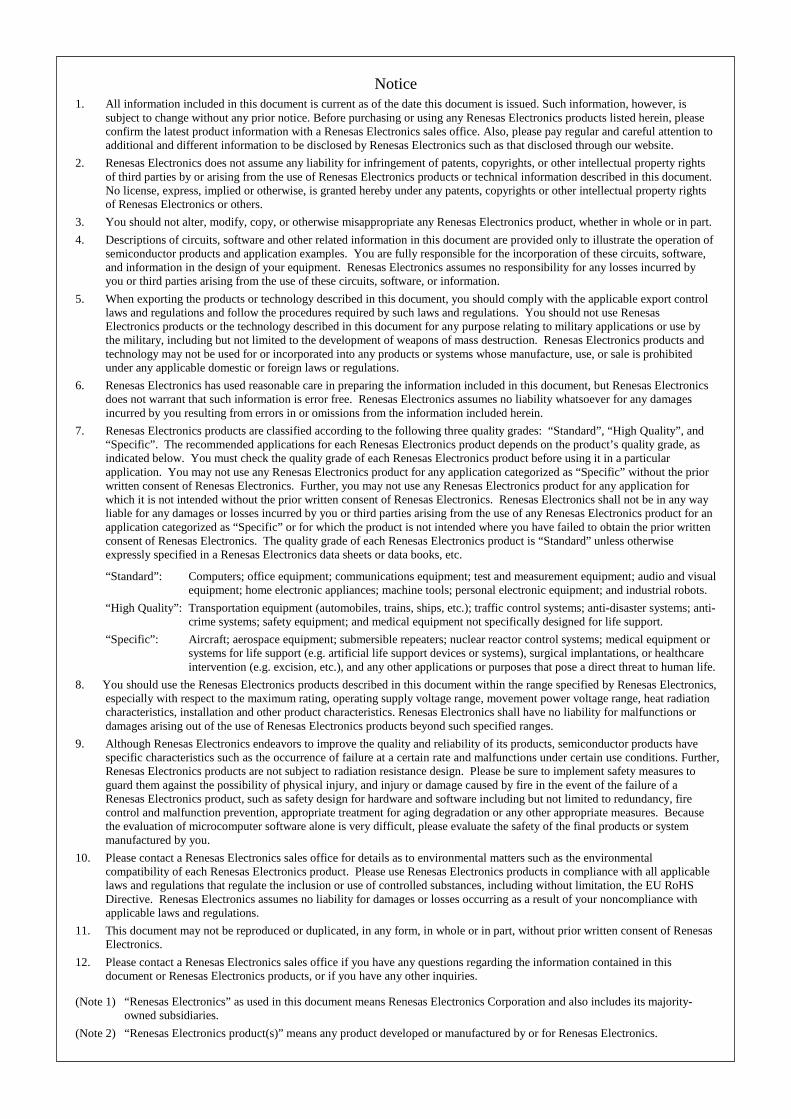
DESCRIPTIONThe 7560 group is the 8-bit microcomputer based on the 740 fam-ily core technology.The 7560 group has the LCD drive control circuit, an 8-channelA-D converter, D-A converter, serial I/O and PWM as additionalfunctions.The various microcomputers in the 7560 group include variationsof internal memory size and packaging. For details, refer to thesection on part numbering.For details on availability of microcomputers in the 7560 group, re-fer the section on group expansion.
FEATURES•Basic machine-language instructions ....................................... 71
•The minimum instruction execution time ............................ 0.5 µs(at 8 MHz oscillation frequency)
•Memory sizeROM ................................................................ 32 K to 60 K bytesRAM ............................................................... 1024 to 2560 bytes
•Programmable input/output ports ............................................. 55
•Software pull-up resistors .................................................... Built-in
•Output ports ................................................................................. 8
• Input ports .................................................................................... 1
•Interrupts .................................................. 17 sources, 16 vectorsExternal ................ 7 sources (includes key input interrupt)Internal ................................................................ 9 sourcesSoftware ................................................................ 1 source
•Timers ............................................................ 8-bit 3, 16-bit 2
•Serial I/O1 ..................... 8-bit 1 (UART or Clock-synchronous)
•Serial I/O2 .................................... 8-bit 1 (Clock-synchronous)
•PWM output .................................................................... 8-bit 1
•A-D converter ................................................ 10-bit 8 channels
•D-A converter .................................................. 8-bit 2 channels
•LCD drive control circuitBias ......................................................................... 1/2, 1/3Duty .................................................................. 1/2, 1/3, 1/4Common output ................................................................ 4Segment output .............................................................. 40
•2 Clock generating circuits(connect to external ceramic resonator or quartz-crystal oscillator)
•Watchdog timer ............................................................. 14-bit 1
•Power source voltage ................................................ 2.2 to 5.5 V(EPROM and One Time PROM version: 2.5 to 5.5 V)
(Extended operating temperature version: 3.0 to 5.5 V)
•Power dissipationIn high-speed mode ........................................................... 32 mW
(at 8 MHz oscillation frequency, at 5 V power source voltage)In low-speed mode.............................................................. 45 µW
(at 32 kHz oscillation frequency, at 3 V power source voltage)
•Operating temperature range ................................... – 20 to 85°C(Extended operating temperature version: – 40 to 85°C)
APPLICATIONSCamera, household appliances, consumer electronics, etc.
7560 GroupMITSUBISHI MICROCOMPUTERS
SINGLE-CHIP 8-BIT CMOS MICROCOMPUTER
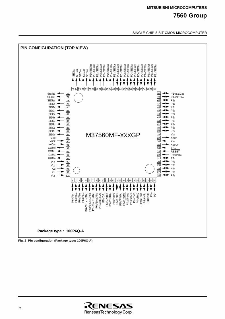
Package type : 100P6S-A
Fig. 1 Pin configuration (Package type: 100P6S-A)
PIN CONFIGURATION (TOP VIEW)
1 2 3 4 5 6 7 8 9 1 0 1
1 1
2 1
3 14 15 16 17 18 1
9 20 2
1 22 23 24 25 26 2
7 2
8 2
9 3
0
3 1
3 2
3 3
3 4
3 5
3 6
3 7
3 8
3 9
4 0
4 1
4 2
4 3
4 4
45
4 6
4 7
4 8
4 9
5 0
51525 35
45
55
65
7585
96
06
162636
46
56
66
76
86
97
0717
27
37
47
57
67
77
87
98
0
8 1
8 2
8 3
8 4
85
8 6
8 7
8 8
8 9
9 0
9 1
9 2
9 3
9 4
9 5
9 6
9 7
9 8
9 9
10 0
M37560MF-XXXFP
S
E
G9
P 31
/
S
E
G1
9
P 30
/
S
E
G1
8
P 32
/
S
E
G2
0
P 33
/
S
E
G2
1
P 34
/
S
E
G2
2
S E
G
1
0
S E
G
1
1
S E
G
1
2
S E
G
1
3
S E
G
1
4
S E
G
1
5
P 35
/
S
E
G2
3
P 36
/
S
E
G2
4
P 37
/
S
E
G2
5
P 00
/
S
E
G2
6
P 01
/
S
E
G2
7
P 02
/
S
E
G2
8
P 03
/
S
E
G2
9
P 04
/
S
E
G3
0
P 05
/
S
E
G3
1
P 06
/
S
E
G3
2
P 07
/
S
E
G3
3
P 10
/
S
E
G3
4
P 11
/
S
E
G3
5
P 12
/
S
E
G3
6
P 13
/
S
E
G3
7
P 14
/
S
E
G3
8
P 15
/
S
E
G3
9
C1
VL
1
P 67
/
A
N7
P 66
/
A
N6
P 65
/
A
N5
P 64
/
A
N4
P 62
/
SC
L
K
2
1/
A
N
2
P 61
/
SO
U
T
2/
A
N
1
P 60
/
SI
N
2/
A
N
0
P 57
/
A
D
T
/
D
A2
P 56
/
D
A1
P 55
/
C
N
T
R1
P 54
/
C
N
T
R0
P 53
/
R
T
P1
P 52
/
R
T
P0
P 51
/
P
W
M1
P 50
/
P
W
M0
P 46
/
SC
L
K
1
P 45
/
TXD
P 44
/
RXD
P 43
/φ/
T
O
U
T
P 42
/
I
N
T2
P 41
/
I
N
T1
P 40
P 77
P 76
P 75
P 74
C2
VL
2
VL
3
C
O
M0
C
O
M1
C
O
M2
VR
E
F
A
VS
S
VC
C
S
E
G8
S
E
G0
S
E
G1
S
E
G2
S
E
G4
S
E
G5
S
E
G6
S
E
G7
S
E
G3
P
72
P
73
P
71
P
70/
I
N
T0
XCIN
XCOUT
XIN
XOUT
VSS
P
27
P
26
P
25
P24
P
23
P
21
P
16
P22
P
20
P
17
R
E
S
E
T
S E
G
1
6
S E
G
1
7
C
O
M3
P 47
/
SR
D
Y
1
P 63
/
SC
L
K
2
2/
A
N
3
SINGLE-CHIP 8-BIT CMOS MICROCOMPUTER
MITSUBISHI MICROCOMPUTERS
7560 Group
2
Package type : 100P6Q-A
PIN CONFIGURATION (TOP VIEW)
Fig. 2 Pin configuration (Package type: 100P6Q-A)
1 2 3 4 5 6 7 8 9 10 11 1 2 1
3 1
4 1
5 1
6 1
7 1
8 1
9 2
0 2
1 2
2 2
3 2
4 2
5
2 6
2 7
2 8
29
30
31
3 2
33
3 4
35
3 6
3 7
3 8
3 9
4 0
41
42
4 3
4 4
45
4 6
4 7
4 8
4 9
5 0
5 15253545556575859606
1626364656
66
76
86
97
07
17
27
37
47
5
76
77
78
79
80
81
82
83
84
85
86
87
88
89
90
91
92
93
94
95
96
97
98
99
0 01
M37560MF-XXXGP
S
E
G1
2
S
E
G1
1
S
E
G1
0
S
E
G9
S
E
G8
S
E
G7
S
E
G6
SEG5
S
E
G4
S
E
G3
SEG2
SEG1
S
E
G0
VCC
VREF
AVSS
C
O
M3
C
O
M2
COM1
COM0
VL
3
VL2
C2
C1
VL
1
P 67
/
A
N7
P 66
/
A
N6
P 65
/
A
N5
P 64
/
A
N4
P 57
/
A
D
T
/
D
A2
P 56
/
D
A1
P 55
/
C
N
T
R1
P 54
/
C
N
T
R0
P 41
/
I
N
T1
P 40
P 43
/φ/
T
O
U
T
P 53
/
R
T
P1
P 52
/
R
T
P0
P 51
/
P
W
M1
P 50
/
P
W
M0
P 77
P 42
/
I
N
T2
P72
P73
P71
P70/INT0
XCIN
XCOUT
XIN
XOUT
VSS
P27
P26
P25
P24
P23
P21
P16
P22
P20
P17
RESET
P76
P75
P74
P15/SEG39
P14/SEG38P
31/
S
E
G
1
9
P 30
/
S
E
G1
8
P 32
/
S
E
G2
0
P 33
/
S
E
G2
1
P 34
/
S
E
G2
2
S E
G
1
3
S E
G
1
4
S E
G
1
5
P 35
/
S
E
G2
3
P 36
/
S
E
G2
4
P 37
/
S
E
G2
5
P 00
/
S
E
G2
6
P 01
/
S
E
G2
7
P 02
/
S
E
G2
8
P 03
/
S
E
G2
9
P 04
/
S
E
G3
0
P 05
/
S
E
G3
1
P 06
/
S
E
G3
2
P 07
/
S
E
G3
3
P 10
/
S
E
G3
4
P 11
/
S
E
G3
5
P 12
/
S
E
G3
6
P 13
/
S
E
G3
7
S E
G
1
6
S E
G
1
7P
62/
S
C
L
K
2
1/
A
N2
P 61
/
SO
U
T
2/
A
N
1
P 60
/
SI
N
2/
A
N
0
P 63
/
SC
L
K
2
2/
A
N
3
P 46
/
SC
L
K
1
P 45
/
TXD
P 4 4
/
RXD
P 47
/
SR
D
Y
1
SINGLE-CHIP 8-BIT CMOS MICROCOMPUTER
MITSUBISHI MICROCOMPUTERS
7560 Group
3
FU
NC
TIO
NA
L B
LO
CK
DIA
GR
AM
(P
acka
ge
typ
e: 1
00P
6S-A
)
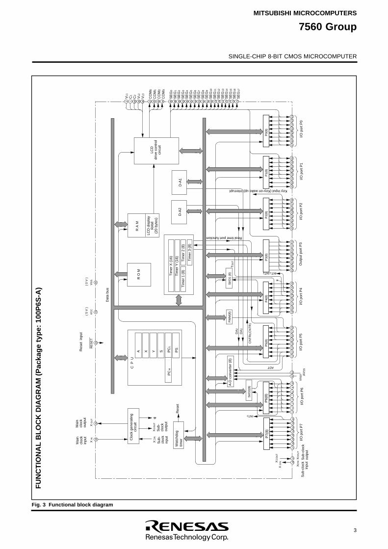
Fig. 3 Functional block diagram
I N
T1
,I
N
T2
C N
T
R
0,
C
N
T
R1
D A
1
A
D
TC
P
U
A X Y S
P C
HP
CL
P SR
E
S
E
TV
C
CV
S
S
( 5
V
)
( 0
V
) R
O
M
R
A
M
3 59 1
4 0
P 4
(
8
)
P 2
(
8
)
P 0
(
8
)
P 1
(
8
)
P 6
(
8
)
P 7
(
8
)
P 3
(
8
)
P 5
(
8
)
12
1 0 0
9 9 9 8 9 7 9 6 9 5 9 4 9 0 8 9 8 8 8 7 8 6 8 5 8 4 8 3 8 2 8 1 8 0 7 9 7 8 7 7 7 6 7 5 7 4 7 3
5 75 8
5 96 0
6 16 2
6 36 4
4 95 0
5 15 2
5 35 4
5 55 6
4 14 2
4 34 4
4 54 6
4 74 8
6 56 6
6 76 8
6 97 0
7 17 2
1 92 0
2 12 2
2 32 4
2 52 6
3 63 7
2 72 8
2 93 0
3 13 2
3 33 4
34
56
78
91 0
9 39 2
1 11 2
1 31 4
1 51 6
1 71 8
XC
I
N
XC
O
U
T
XI N
O U
T
X
C O
U
T
XX
C I
N
S I
/
O
1
(
8
)
VR
E
F A V
S
S
VL
1
C1
C2
VL
2
VL
3
C O
M
0
C O
M
1
C O
M
2
C O
M
3
S E
G
0
S E
G
1
S E
G
2
S E
G
3
S E
G
4
S E
G
5
S E
G
6
S E
G
7
S E
G
8
S E
G
9
S E
G
1
0
S E
G
1
1
S E
G
1
2
S E
G
1
3
S E
G
1
4
S E
G
1
5
S E
G
1
6
S E
G
1
7
φ
XC
I
N
C O
U
T
X
3 83 9
S I
/
O
2
(
8
)
P W
M
(
8
)
φ
I N
T0
D -
A
2
D -
A
1
D A
2
TO
U
T
L
C
Dd
r
i
v
e
c
o
n
t
r
o
lc
i
r
c
u
i
t
L
C
D
d
i
s
p
l
a
yR
A
M(
2
0
b
y
t
e
s
)
T
i
m
e
r
X
(
1
6
)
T
i
m
e
r
Y
(
1
6
)
T
i
m
e
r
1
(
8
)T
i
m
e
r
2
(
8
)
T i
m
e
r
3
(
8
)
D a
t
a
b
u
s
C
l
o
c
k
g
e
n
e
r
a
t
i
n
gc
i
r
c
u
i
t
M a
i
n
c l
o
c
ki n
p
u
t
M a
i
n
cl
o
c
ko u
t
p
u
t
S u
b
-
c
l
o
c
k
o u
t
p
u
tS
u
b
-
c
l
o
c
k
i
n
p
u
t
R e
s
e
t
K
e
y
i
n
p
u
t
(
K
e
y
-
o
n
w
a
k
e
u
p
)
i
n
t
e
r
r
u
p
t
R
e
a
l
t
i
m
e
p
o
r
t
f
u
n
c
t
i
o
n
A -
D
c
o
n
v
e
r
t
e
r
(
8
)
I
/
O
p
o
r
t
P
0I
/
O
p
o
r
t
P
1
I
/
O
p
o
r
t
P
2I
/
O
p
o
r
t
P
4
I
/
O
p
o
r
t
P
5I
/
O
p
o
r
t
P
6
O
u
t
p
u
t
p
o
r
t
P
3I
/
O
p
o
r
t
P
7
R e
s
e
t
i
n
p
u
t
S u
b
-
c l
o
c
ko u
t
p
u
t
S u
b
-
c l
o
c
ki n
p
u
t
W a
t
c
h
d
o
g
t i m
e
r
SINGLE-CHIP 8-BIT CMOS MICROCOMPUTER
MITSUBISHI MICROCOMPUTERS
7560 Group
4
PIN DESCRIPTIONTable 1 Pin description (1)
VCC, VSS
FunctionPin NameFunction except a port function
•LCD segment output pins
Power source •Apply voltage of 2.2 V to 5.5 V (2.5 to 5.5 V for EPROM and One Time PROM version, 3.0 to 5.5 Vfor extended operating temperature version) to VCC, and 0 V to VSS.
VREF
AVSS
RESET
XIN
XOUT
VL1–VL3
C1, C2
COM0–COM3
SEG0–SEG17
P00/SEG26–P07/SEG33
P10/SEG34–P15/SEG39
P16, P17
P20 – P27
P30/SEG18 –P37/SEG25
Analog refer-ence voltage
Analog powersource
Reset input
Clock input
Clock output
LCD powersource
Charge-pumpcapacitor pin
Common output
Segment output
I/O port P0
I/O port P1
I/O port P2
Output port P3
•Reference voltage input pin for A-D converter and D-A converter.
•GND input pin for A-D converter and D-A converter.
•Connect to VSS.
•Reset input pin for active “L”.
•Input and output pins for the main clock generating circuit.
•Connect a ceramic resonator or a quartz-crystal oscillator between the XIN and XOUT pins to setthe oscillation frequency.
•If an external clock is used, connect the clock source to the XIN pin and leave the XOUT pin open. Afeedback resistor is built-in.
•Input 0 ≤ VL1 ≤ VL2 ≤ VL3 voltage.
•Input 0 – VL3 voltage to LCD. (0 ≤ VL1 ≤ VL2 ≤ VL3 when a voltage is multiplied.)
•External capacitor pins for a voltage multiplier (3 times) of LCD control.
•LCD common output pins.
•COM2 and COM3 are not used at 1/2 duty ratio.
•COM3 is not used at 1/3 duty ratio.
•LCD segment output pins.
•8-bit I/O port.
•CMOS compatible input level.
•CMOS 3-state output structure.
•Pull-up control is enabled.
•I/O direction register allows each 8-bit pin to be pro-grammed as either input or output.
•6-bit I/O port.
•CMOS compatible input level.
•CMOS 3-state output structure.
•Pull-up control is enabled.
•I/O direction register allows each 6-bit pin to be pro-grammed as either input or output.
•2-bit I/O port.
•CMOS compatible input level.
•CMOS 3-state output structure.
•I/O direction register allows each pin to be individually programmed as either input or output.
•Pull-up control is enabled.•8-bit I/O port.
•CMOS compatible input level.
•CMOS 3-state output structure.
•I/O direction register allows each pin to be individually
programmed as either input or output.
•Pull-up control is enabled.
•8-bit output.
•CMOS 3-state output structure.
•Port output control is enabled.
•Key input (key-on wake-up) interruptinput pins
•LCD segment output pins
SINGLE-CHIP 8-BIT CMOS MICROCOMPUTER
MITSUBISHI MICROCOMPUTERS
7560 Group
5
Table 2 Pin description (2)
FunctionPin NameFunction except a port function
P40
P41/INT1,P42/INT2
P43/φ/TOUT
P44/RXD,P45/TXD,P46/SCLK1,P47/SRDY1
P50/PWM0,P51/PWM1
P52/RTP0,P53/RTP1
P54/CNTR0,P55/CNTR1
P56/DA1
P57/ADT/DA2
P60/SIN2/AN0,P61/SOUT2/AN1,P62/SCLK21/AN2,P63/SCLK22/AN3
P64/AN4–P67/AN7
P70/INT0
P71–P77
I/O port P4
I/O port P5
I/O port P6
Input port P7
I/O port P7
Sub-clock output
Sub-clock input
•1-bit I/O port.
•CMOS compatible input level.
•N-channel open-drain output structure.
•I/O direction register allows this pin to be individually programmed as either input or output.
•7-bit I/O port.
•CMOS compatible input level.
•CMOS 3-state output structure.
•I/O direction register allows each pin to be individuallyprogrammed as either input or output.
•Pull-up control is enabled.
•8-bit I/O port.
•CMOS compatible input level.
•CMOS 3-state output structure.
•I/O direction register allows each pin to be individuallyprogrammed as either input or output.
•Pull-up control is enabled.
•8-bit I/O port.
•CMOS compatible input level.
•CMOS 3-state output structure.
•I/O direction register allows each pin to be individuallyprogrammed as either input or output.
•Pull-up control is enabled.
•1-bit input port.
•INTi interrupt input pins
•System clock φ output pin
•Timer 2 output pin
•Serial I/O1 I/O pins
•PWM output pins
•Real time port output pins
•Timer X, Y I/O pins
•D-A converter output pin
•D-A converter output pin
•A-D external trigger input pin
•A-D converter input pins
•Serial I/O2 I/O pins
•A-D converter input pins
XCOUT
XCIN
•INT0 interrupt input pin
•7-bit I/O port.
•CMOS compatible input level.
•N-channel open-drain output structure.
•I/O direction register allows each pin to be individually programmed as either input or output.
•Sub-clock generating circuit I/O pins.
(Connect a oscillator. External clock cannot be used.)
SINGLE-CHIP 8-BIT CMOS MICROCOMPUTER
MITSUBISHI MICROCOMPUTERS
7560 Group
6
PART NUMBERING
Fig. 4 Part numbering
M
3
7
5
6
0
M
F
D
–
X
X
X
F
PProduct
ROM/PROM size123456789ABCDEF
: 4096 bytes: 8192 bytes: 12288 bytes: 16384 bytes: 20480 bytes: 24576 bytes: 28672 bytes: 32768 bytes: 36864 bytes: 40960 bytes: 45056 bytes: 49152 bytes: 53248 bytes: 57344 bytes: 61440 bytes
T
h
e
f
i
r
s
t
1
2
8
b
y
t
e
s
a
n
d
t
h
e
l
a
s
t
2
b
y
t
e
s
o
f
R
O
M
a
r
e
r
e
s
e
r
v
e
d
a
r
e
a
s
;
t
h
e
y
c
a
n
n
o
t
b
e
u
s
e
d
.
Memory typeME
: Mask ROM version: EPROM and One Time PROM version
ROM number
P
a
c
k
a
g
e
t
y
p
eF
PG
PF
S
: 100P6S-A: 100P6Q-A: 100D0
D :Extended operating temperature version
Omitted in One Time PROM version and EPROM version.
Omitted in standard version.
SINGLE-CHIP 8-BIT CMOS MICROCOMPUTER
MITSUBISHI MICROCOMPUTERS
7560 Group
7
GROUP EXPANSIONMitsubishi expands the 7560 group as follows.
Memory TypeSupport for mask ROM version.
Memory SizeROM size ........................................................... 32 K to 60 K bytesRAM size .......................................................... 1024 to 2560 bytes
Packages100P6Q-A .................................. 0.5 mm-pitch plastic molded QFP100P6S-A ................................ 0.65 mm-pitch plastic molded QFP
Memory Expansion
Fig. 5 Memory expansion
ROM size (bytes)
RAM size (bytes)
256 5 1
2 7
6
8 1024 1280 1
5
3
6 17921
9
2 2
0
4
8 2
3
0
4 2560
32K
28K
24K
20K
16K
1
2
K
8
K
4K
5
2
K
4
8
K
4
4
K
4
0
K
3
6
K
5
6
K
6
0
K M
3
7
5
6
0
M
F
M
a
s
s
p
r
o
d
u
c
t
M37560M8
M
a
s
s
p
r
o
d
u
c
t
Currently products are listed below.
Table 3 List of products As of Jan. 2003
Remarks
Mask ROM version
Mask ROM version
Mask ROM version
Mask ROM version
Package
100P6S-A
100P6Q-A
100P6S-A
100P6Q-A
Product
M37560M8-XXXFP
M37560M8-XXXGP
M37560MF-XXXFP
M37560MF-XXXGP
RAM size (bytes)
102432768
(32638)
61440(61310)
ROM size (bytes)ROM size for User in ( )
2560
SINGLE-CHIP 8-BIT CMOS MICROCOMPUTER
MITSUBISHI MICROCOMPUTERS
7560 Group
8
GROUP EXPANSION(One Time and EPROM version)Mitsubishi expands the 7560 group as follows.
Memory TypeSupport for One Time and EPROM version.
Memory SizeROM size ........................................................................ 60 K bytesRAM size ....................................................................... 2560 bytes
Packages100P6Q-A .................................. 0.5 mm-pitch plastic molded QFP100P6S-A ................................ 0.65 mm-pitch plastic molded QFP100D0 .......................................... Ceramic LCC (EPROM version)
Memory Expansion
Fig. 6 Memory expansion
Currently products are listed below.
Table 4 List of products As of Jan. 2003
Remarks
One Time PROM version
One Time PROM version
EPROM version
Package
100P6S-A
100P6Q-A
100D0
Product
M37560EFFP
M37560EFGP
M37560EFFS
RAM size (bytes)
61440(61310)
ROM size (bytes)ROM size for User in ( )
2560
R
O
M
s
i
z
e
(
b
y
t
e
s
)
RAM size (bytes)
2 5
6 5
1
2 768 1
0
2
4 1280 1536 17921
9
2 2
0
4
8 2304 2560
32K
28K
24K
20K
16K
1
2
K
8
K
4K
5
2
K
4
8
K
4
4
K
4
0
K
3
6
K
5
6
K
6
0
K M
3
7
5
6
0
E
F
Mass product
SINGLE-CHIP 8-BIT CMOS MICROCOMPUTER
MITSUBISHI MICROCOMPUTERS
7560 Group
9
GROUP EXPANSION(Extended operating temperature version)Mitsubishi expands the 7560 group as follows.
Memory TypeSupport for extended operating temperature version.
Memory SizeROM size ........................................................................ 60 K bytesRAM size ....................................................................... 2560 bytes
Packages100P6S-A ................................ 0.65 mm-pitch plastic molded QFP
Memory Expansion
Fig. 7 Memory expansion
Currently products are listed below.
Table 5 List of products As of Jan. 2003
Remarks
Mask ROM version (Extended operating temperature version)
One Time PROM version
(Extended operating temperature version)
PackageProduct
M37560MFD-XXXFP
M37560EFDFP
RAM size (bytes)
61440(61310)
ROM size (bytes)ROM size for User in ( )
2560 100P6S-A
ROM size (bytes)
RAM size (bytes)
256 512 768 1024 1280 1536 1792192 2048 2304 2560
32K
28K
24K
20K
16K
12K
8
K
4K
5
2
K
48K
44K
4
0
K
36K
56K
60K M37560EFDM37560MFD
Mass product
SINGLE-CHIP 8-BIT CMOS MICROCOMPUTER
MITSUBISHI MICROCOMPUTERS
7560 Group
10
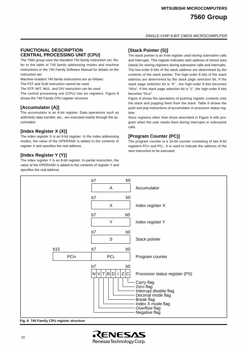
FUNCTIONAL DESCRIPTIONCENTRAL PROCESSING UNIT (CPU)The 7560 group uses the standard 740 family instruction set. Re-fer to the table of 740 family addressing modes and machineinstructions or the 740 Family Software Manual for details on theinstruction set.Machine-resident 740 family instructions are as follows:The FST and SLW instruction cannot be used.The STP, WIT, MUL, and DIV instruction can be used.The central processing unit (CPU) has six registers. Figure 8shows the 740 Family CPU register structure.
[Accumulator (A)]The accumulator is an 8-bit register. Data operations such asarithmetic data transfer, etc., are executed mainly through the ac-cumulator.
[Index Register X (X)]The index register X is an 8-bit register. In the index addressingmodes, the value of the OPERAND is added to the contents ofregister X and specifies the real address.
[Index Register Y (Y)]The index register Y is an 8-bit register. In partial instruction, thevalue of the OPERAND is added to the contents of register Y andspecifies the real address.
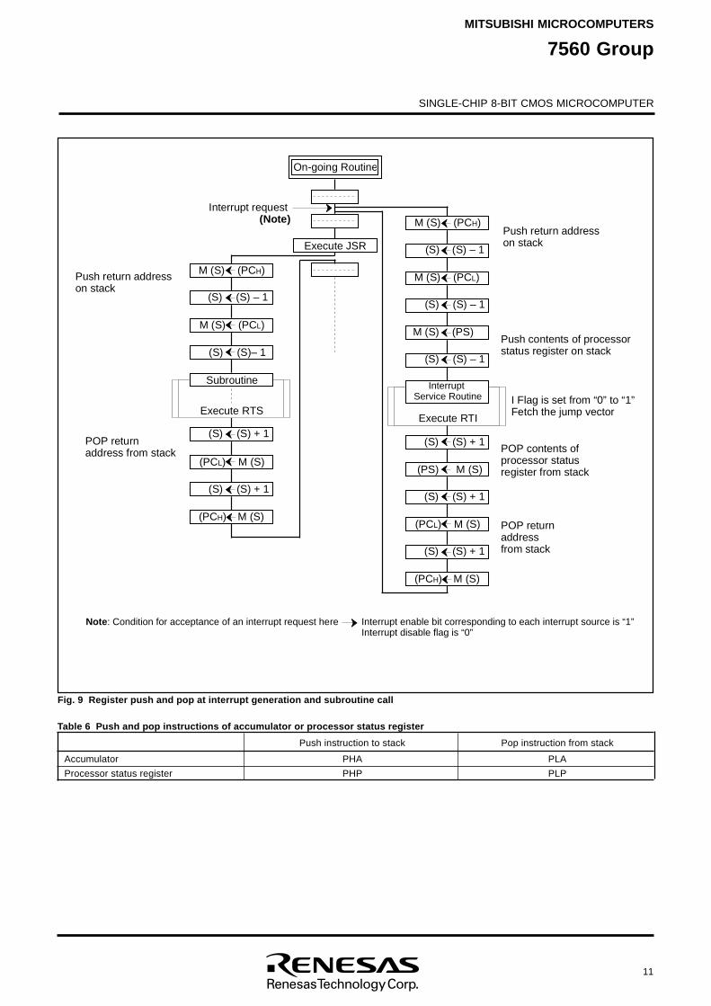
[Stack Pointer (S)]The stack pointer is an 8-bit register used during subroutine callsand interrupts. This register indicates start address of stored area(stack) for storing registers during subroutine calls and interrupts.The low-order 8 bits of the stack address are determined by thecontents of the stack pointer. The high-order 8 bits of the stackaddress are determined by the stack page selection bit. If thestack page selection bit is “0” , the high-order 8 bits becomes“0016”. If the stack page selection bit is “1”, the high-order 8 bitsbecomes “0116”.Figure 9 shows the operations of pushing register contents ontothe stack and popping them from the stack. Table 6 shows thepush and pop instructions of accumulator or processor status reg-ister.Store registers other than those described in Figure 9 with pro-gram when the user needs them during interrupts or subroutinecalls.
[Program Counter (PC)]The program counter is a 16-bit counter consisting of two 8-bitregisters PCH and PCL. It is used to indicate the address of thenext instruction to be executed.
Fig. 8 740 Family CPU register structure
A Accumulator
b7
b7
b7
b7 b0
b7b15 b0
b7 b0
b0
b0
b0
X Index register X
Y Index register Y
S Stack pointer
PCL Program counterPCH
N V T B D I Z C Processor status register (PS)
Carry flagZero flagInterrupt disable flagDecimal mode flagBreak flagIndex X mode flagOverflow flagNegative flag
SINGLE-CHIP 8-BIT CMOS MICROCOMPUTER
MITSUBISHI MICROCOMPUTERS
7560 Group
11
Table 6 Push and pop instructions of accumulator or processor status register
Accumulator
Processor status register
Push instruction to stack
PHA
PHP
Pop instruction from stack
PLA
PLP
Fig. 9 Register push and pop at interrupt generation and subroutine call
N
o
t
e:
C
o
n
d
i
t
i
o
n
f
o
r
a
c
c
e
p
t
a
n
c
e
o
f
a
n
i
n
t
e
r
r
u
p
t
r
e
q
u
e
s
t
h
e
r
e
E
x
e
c
u
t
e
J
S
R
On-going Routine
M
(
S
) (
P
CH)
( S
)
(
S
)
–
1
M
(
S
) (
P
CL)
E
x
e
c
u
t
e
R
T
S
(PCL) M (S)
( S
)
(
S
)
–
1
( S
)
(
S
)
+
1
( S
)
(
S
)
+
1
(PCH) M (S)
S
u
b
r
o
u
t
i
n
e
POP returnaddress from stack
P
u
s
h
r
e
t
u
r
n
a
d
d
r
e
s
s
o
n
s
t
a
c
k
M (S) (PS)
Execute RTI
( P
S
) M
(
S
)
(S) (S) – 1
(S) (S) + 1
Interrupt Service Routine
POP contents of processor status register from stack
M
(
S
) (
P
CH)
(S)
(
S
)
–
1
M
(
S
) (
P
CL)
(S) (S) – 1
(PCL) M (S)
(S) (S) + 1
(S) (S) + 1
( P
CH) M
(
S
)
POP returnaddress from stack
I
F
l
a
g
i
s
s
e
t
f
r
o
m
“
0
”
t
o
“
1
”
F
e
t
c
h
t
h
e
j
u
m
p
v
e
c
t
o
r
P
u
s
h
r
e
t
u
r
n
a
d
d
r
e
s
s
o
n
s
t
a
c
k
Push contents of processor status register on stack
Interrupt request (
N
o
t
e
)
I n
t
e
r
r
u
p
t
e
n
a
b
l
e
b
i
t
c
o
r
r
e
s
p
o
n
d
i
n
g
t
o
e
a
c
h
i
n
t
e
r
r
u
p
t
s
o
u
r
c
e
i
s
“
1
”
I
n
t
e
r
r
u
p
t
d
i
s
a
b
l
e
f
l
a
g
i
s
“
0
”
SINGLE-CHIP 8-BIT CMOS MICROCOMPUTER
MITSUBISHI MICROCOMPUTERS
7560 Group
12
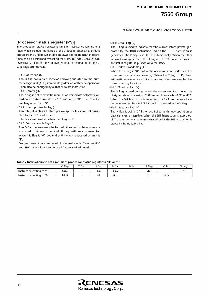
[Processor status register (PS)]The processor status register is an 8-bit register consisting of 5flags which indicate the status of the processor after an arithmeticoperation and 3 flags which decide MCU operation. Branch opera-tions can be performed by testing the Carry (C) flag , Zero (Z) flag,Overflow (V) flag, or the Negative (N) flag. In decimal mode, the Z,V, N flags are not valid.
• Bit 0: Carry flag (C)The C flag contains a carry or borrow generated by the arith-metic logic unit (ALU) immediately after an arithmetic operation.It can also be changed by a shift or rotate instruction.
• Bit 1: Zero flag (Z)The Z flag is set to “1” if the result of an immediate arithmetic op-eration or a data transfer is “0”, and set to “0” if the result isanything other than “0”.
• Bit 2: Interrupt disable flag (I)The I flag disables all interrupts except for the interrupt gener-ated by the BRK instruction.Interrupts are disabled when the I flag is “1”.
• Bit 3: Decimal mode flag (D)The D flag determines whether additions and subtractions areexecuted in binary or decimal. Binary arithmetic is executedwhen this flag is “0”; decimal arithmetic is executed when it is“1”.Decimal correction is automatic in decimal mode. Only the ADCand SBC instructions can be used for decimal arithmetic.
• Bit 4: Break flag (B)The B flag is used to indicate that the current interrupt was gen-erated by the BRK instruction. When the BRK instruction isgenerated, the B flag is set to “1” automatically. When the otherinterrupts are generated, the B flag is set to “0”, and the proces-sor status register is pushed onto the stack.
• Bit 5: Index X mode flag (T)When the T flag is “0”, arithmetic operations are performed be-tween accumulator and memory. When the T flag is “1”, directarithmetic operations and direct data transfers are enabled be-tween memory locations.
• Bit 6: Overflow flag (V)The V flag is used during the addition or subtraction of one byteof signed data. It is set to “1” if the result exceeds +127 to -128.When the BIT instruction is executed, bit 6 of the memory loca-tion operated on by the BIT instruction is stored in the V flag.
• Bit 7: Negative flag (N)The N flag is set to “1” if the result of an arithmetic operation ordata transfer is negative. When the BIT instruction is executed,bit 7 of the memory location operated on by the BIT instruction isstored in the negative flag.
Table 7 Instructions to set each bit of processor status register to “0” or “1”
Instruction setting to “1”
Instruction setting to “0”
C flag
SEC
CLC
Z flag
–
–
I flag
SEI
CLI
D flag
SED
CLD
B flag
–
–
T flag
SET
CLT
V flag
–
CLV
N flag
–
–
SINGLE-CHIP 8-BIT CMOS MICROCOMPUTER
MITSUBISHI MICROCOMPUTERS
7560 Group
13
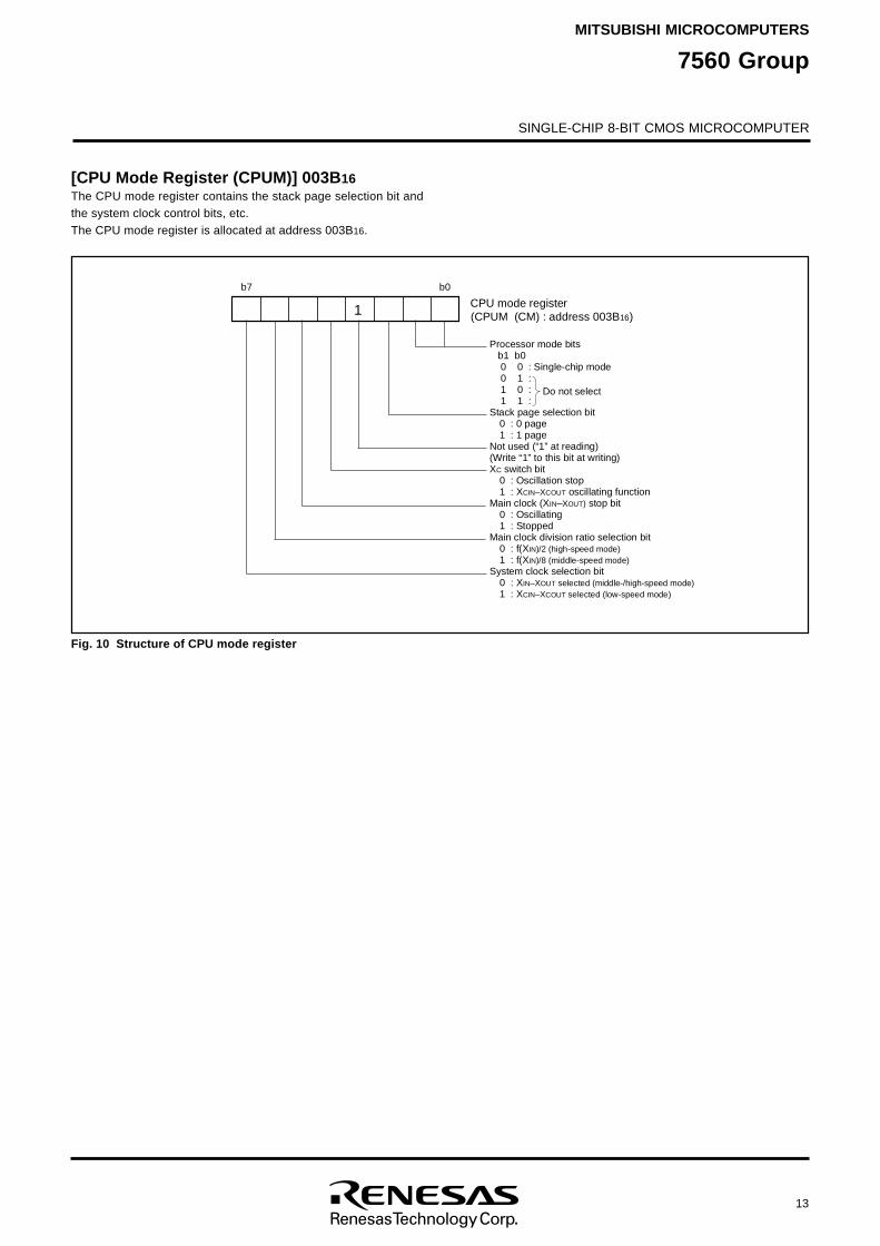
[CPU Mode Register (CPUM)] 003B16The CPU mode register contains the stack page selection bit andthe system clock control bits, etc.The CPU mode register is allocated at address 003B16.
Fig. 10 Structure of CPU mode register
Processor mode bits b1 b0 0 0 : Single-chip mode 0 1 : 1 0 : 1 1 :Stack page selection bit
0 : 0 page1 : 1 page
Not used (“1” at reading)(Write “1” to this bit at writing)XC switch bit
0 : Oscillation stop1 : XCIN–XCOUT oscillating function
Main clock (XIN–XOUT) stop bit0 : Oscillating1 : Stopped
Main clock division ratio selection bit0 : f(XIN)/2 (high-speed mode)1 : f(XIN)/8 (middle-speed mode)
System clock selection bit0 : XIN–XOUT selected (middle-/high-speed mode)1 : XCIN–XCOUT selected (low-speed mode)
Do not select
C
P
U
m
o
d
e
r
e
g
i
s
t
e
r(CPUM (CM) : address 003B16)
b
7 b
0
1
SINGLE-CHIP 8-BIT CMOS MICROCOMPUTER
MITSUBISHI MICROCOMPUTERS
7560 Group
14
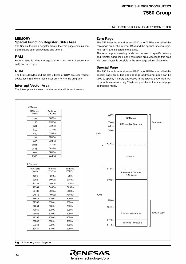
MEMORYSpecial Function Register (SFR) AreaThe Special Function Register area in the zero page contains con-trol registers such as I/O ports and timers.
RAMRAM is used for data storage and for stack area of subroutinecalls and interrupts.
ROMThe first 128 bytes and the last 2 bytes of ROM are reserved fordevice testing and the rest is user area for storing programs.
Interrupt Vector AreaThe interrupt vector area contains reset and interrupt vectors.
Zero PageThe 256 bytes from addresses 000016 to 00FF16 are called thezero page area. The internal RAM and the special function regis-ters (SFR) are allocated to this area.The zero page addressing mode can be used to specify memoryand register addresses in the zero page area. Access to this areawith only 2 bytes is possible in the zero page addressing mode.
Special PageThe 256 bytes from addresses FF0016 to FFFF16 are called thespecial page area. The special page addressing mode can beused to specify memory addresses in the special page area. Ac-cess to this area with only 2 bytes is possible in the special pageaddressing mode.
Fig. 11 Memory map diagram
1
9
2
2
5
6
3
8
4
5
1
2
6
4
0
7
6
8
8
9
6
1
0
2
4
1
5
3
6
2
0
4
8
2
5
6
0
00FF16
013F16
01BF16
023F16
02BF16
033F16
03BF16
043F16
063F16
083F16
0A3F16
R
A
M
a
r
e
a
R
A
M
s
i
z
e(
b
y
t
e
s
)A
d
d
r
e
s
s
X
X
X
X1
6
4
0
9
6
8
1
9
2
1
2
2
8
8
1
6
3
8
4
2
0
4
8
0
2
4
5
7
6
2
8
6
7
2
3
2
7
6
8
3
6
8
6
4
4
0
9
6
0
4
5
0
5
6
4
9
1
5
2
5
3
2
4
8
5
7
3
4
4
6
1
4
4
0
F
0
0
01
6
E
0
0
01
6
D
0
0
01
6
C
0
0
01
6
B
0
0
01
6
A
0
0
01
6
9
0
0
01
6
8
0
0
01
6
7
0
0
01
6
6
0
0
01
6
5
0
0
01
6
4
0
0
01
6
3
0
0
01
6
2
0
0
01
6
1
0
0
01
6
F
0
8
01
6
E
0
8
01
6
D
0
8
01
6
C
0
8
01
6
B
0
8
01
6
A
0
8
01
6
9
0
8
01
6
8
0
8
01
6
7
0
8
01
6
6
0
8
01
6
5
0
8
01
6
4
0
8
01
6
3
0
8
01
6
2
0
8
01
6
1
0
8
01
6
ROM area
ROM size(bytes)
A
d
d
r
e
s
sY
Y
Y
Y1
6
A
d
d
r
e
s
sZ
Z
Z
Z1
6
010016
000016
004016
FF0016
FFDC16
F
F
F
E1
6
FFFF16
XXXX16
YYYY16
ZZZZ16
RAM
R
O
M
005416
S
F
R
a
r
e
a
N
o
t
u
s
e
d
I n
t
e
r
r
u
p
t
v
e
c
t
o
r
a
r
e
a
Reserved ROM area(128 bytes)
Z
e
r
o
p
a
g
e
S
p
e
c
i
a
l
p
a
g
e
LCD display RAM area
R
e
s
e
r
v
e
d
R
O
M
a
r
e
a
SINGLE-CHIP 8-BIT CMOS MICROCOMPUTER
MITSUBISHI MICROCOMPUTERS
7560 Group
15
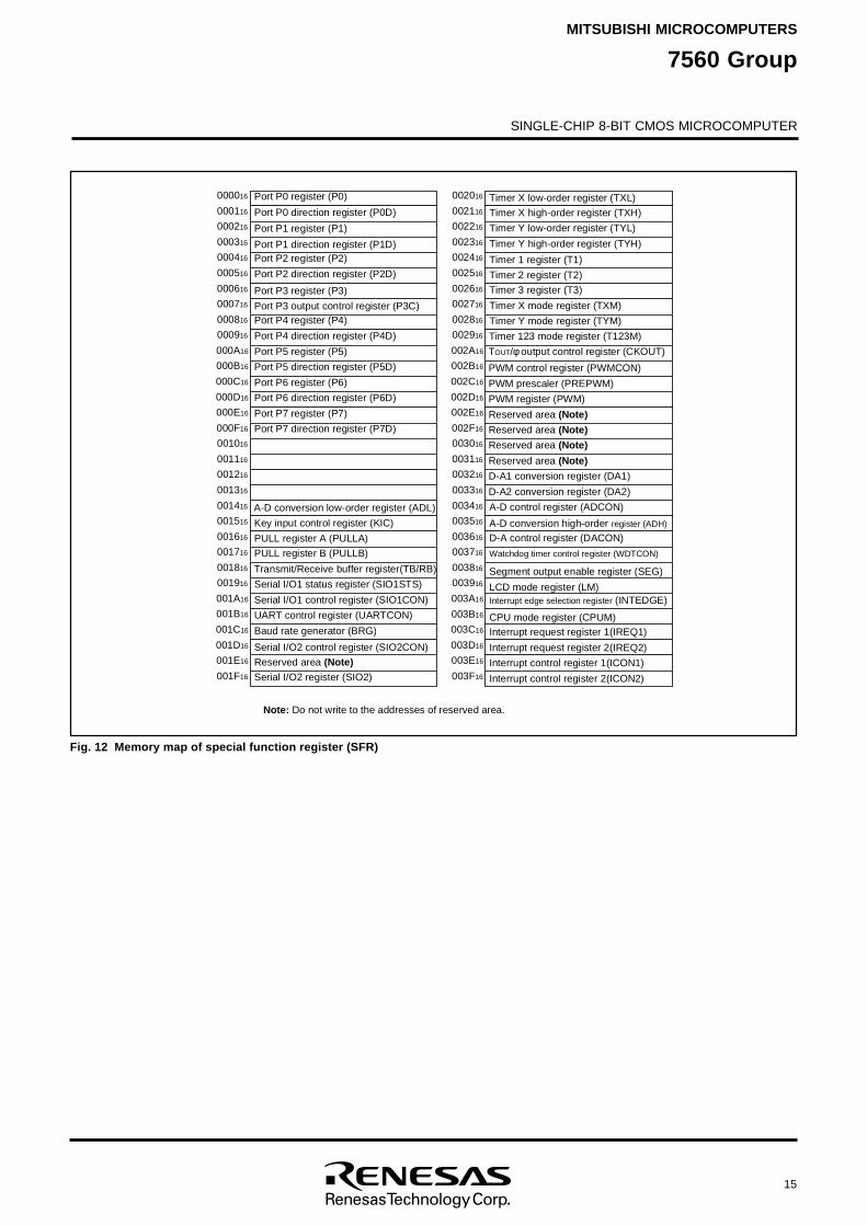
Fig. 12 Memory map of special function register (SFR)
0
0
2
01
6
0
0
2
11
6
0
0
2
21
6
0
0
2
31
6
0
0
2
41
6
002516
0
0
2
61
6
0
0
2
71
6
0
0
2
81
6
0
0
2
91
6
0
0
2
A1
6
0
0
2
B1
6
002C16
002D16
0
0
2
E1
6
002F16
0
0
3
01
6
0
0
3
11
6
0
0
3
21
6
0
0
3
31
6
003416
0
0
3
51
6
003616
003716
003816
003916
003A16
0
0
3
B1
6
003C16
003D16
0
0
3
E1
6
003F16
0
0
0
01
6
0
0
0
11
6
0
0
0
21
6
0
0
0
31
6
0
0
0
41
6
000516
0
0
0
61
6
0
0
0
71
6
0
0
0
81
6
0
0
0
91
6
0
0
0
A1
6
0
0
0
B1
6
0
0
0
C1
6
0
0
0
D1
6
0
0
0
E1
6
0
0
0
F1
6
0
0
1
01
6
0
0
1
11
6
0
0
1
21
6
0
0
1
31
6
001416
0
0
1
51
6
001616
001716
001816
001916
001A16
001B16
001C16
001D16
0
0
1
E1
6
0
0
1
F1
6
P
o
r
t
P
0
r
e
g
i
s
t
e
r
(
P
0
)
P
o
r
t
P
1
r
e
g
i
s
t
e
r
(
P
1
)
Port P1 direction register (P1D)P
o
r
t
P
2
r
e
g
i
s
t
e
r
(
P
2
)
P
o
r
t
P
2
d
i
r
e
c
t
i
o
n
r
e
g
i
s
t
e
r
(
P
2
D
)
Port P3 register (P3)
P
o
r
t
P
4
r
e
g
i
s
t
e
r
(
P
4
)
P
o
r
t
P
4
d
i
r
e
c
t
i
o
n
r
e
g
i
s
t
e
r
(
P
4
D
)
P
o
r
t
P
5
r
e
g
i
s
t
e
r
(
P
5
)
P
o
r
t
P
5
d
i
r
e
c
t
i
o
n
r
e
g
i
s
t
e
r
(
P
5
D
)
P
o
r
t
P
6
r
e
g
i
s
t
e
r
(
P
6
)
P
o
r
t
P
6
d
i
r
e
c
t
i
o
n
r
e
g
i
s
t
e
r
(
P
6
D
)
P
o
r
t
P
7
r
e
g
i
s
t
e
r
(
P
7
)
P
o
r
t
P
7
d
i
r
e
c
t
i
o
n
r
e
g
i
s
t
e
r
(
P
7
D
)
S
e
r
i
a
l
I
/
O
1
s
t
a
t
u
s
r
e
g
i
s
t
e
r
(
S
I
O
1
S
T
S
)
Serial I/O1 control register (SIO1CON)
U
A
R
T
c
o
n
t
r
o
l
r
e
g
i
s
t
e
r
(
U
A
R
T
C
O
N
)
Baud rate generator (BRG)
I n
t
e
r
r
u
p
t
c
o
n
t
r
o
l
r
e
g
i
s
t
e
r
2
(
I
C
O
N
2
)
T
i
m
e
r
3
r
e
g
i
s
t
e
r
(
T
3
)
T
i
m
e
r
X
m
o
d
e
r
e
g
i
s
t
e
r
(
T
X
M
)
I n
t
e
r
r
u
p
t
e
d
g
e
s
e
l
e
c
t
i
o
n
r
e
g
i
s
t
e
r
(
I
N
T
E
D
G
E
)
CPU mode register (CPUM)Interrupt request register 1(IREQ1)
Interrupt request register 2(IREQ2)
I n
t
e
r
r
u
p
t
c
o
n
t
r
o
l
r
e
g
i
s
t
e
r
1
(
I
C
O
N
1
)
T
i
m
e
r
X
l
o
w
-
o
r
d
e
r
r
e
g
i
s
t
e
r
(
T
X
L
)
T
i
m
e
r
Y
l
o
w
-
o
r
d
e
r
r
e
g
i
s
t
e
r
(
T
Y
L
)
Timer 1 register (T1)
T
i
m
e
r
2
r
e
g
i
s
t
e
r
(
T
2
)
Timer X high-order register (TXH)
T
i
m
e
r
Y
h
i
g
h
-
o
r
d
e
r
r
e
g
i
s
t
e
r
(
T
Y
H
)
P
U
L
L
r
e
g
i
s
t
e
r
A
(
P
U
L
L
A
)
P
U
L
L
r
e
g
i
s
t
e
r
B
(
P
U
L
L
B
)
T
i
m
e
r
Y
m
o
d
e
r
e
g
i
s
t
e
r
(
T
Y
M
)
Timer 123 mode register (T123M)
TO
U
T/φ
o
u
t
p
u
t
c
o
n
t
r
o
l
r
e
g
i
s
t
e
r
(
C
K
O
U
T
)
Segment output enable register (SEG)
LCD mode register (LM)
A
-
D
c
o
n
t
r
o
l
r
e
g
i
s
t
e
r
(
A
D
C
O
N
)
A-D conversion high-order register (ADH)
Transmit/Receive buffer register(TB/RB)
K
e
y
i
n
p
u
t
c
o
n
t
r
o
l
r
e
g
i
s
t
e
r
(
K
I
C
)
P
o
r
t
P
0
d
i
r
e
c
t
i
o
n
r
e
g
i
s
t
e
r
(
P
0
D
)
P
o
r
t
P
3
o
u
t
p
u
t
c
o
n
t
r
o
l
r
e
g
i
s
t
e
r
(
P
3
C
)
Reserved area (Note)S
e
r
i
a
l
I
/
O
2
c
o
n
t
r
o
l
r
e
g
i
s
t
e
r
(
S
I
O
2
C
O
N
)
S
e
r
i
a
l
I
/
O
2
r
e
g
i
s
t
e
r
(
S
I
O
2
)
P
W
M
c
o
n
t
r
o
l
r
e
g
i
s
t
e
r
(
P
W
M
C
O
N
)
PWM prescaler (PREPWM)
PWM register (PWM)
Reserved area (Note)
Reserved area (Note)
R
e
s
e
r
v
e
d
a
r
e
a
(
N
o
t
e
)
Reserved area (Note)
D
-
A
1
c
o
n
v
e
r
s
i
o
n
r
e
g
i
s
t
e
r
(
D
A
1
)
D-A2 conversion register (DA2)
D-A control register (DACON)
W
a
t
c
h
d
o
g
t
i
m
e
r
c
o
n
t
r
o
l
r
e
g
i
s
t
e
r
(
W
D
T
C
O
N
)
Note: Do not write to the addresses of reserved area.
A
-
D
c
o
n
v
e
r
s
i
o
n
l
o
w
-
o
r
d
e
r
r
e
g
i
s
t
e
r
(
A
D
L
)
SINGLE-CHIP 8-BIT CMOS MICROCOMPUTER
MITSUBISHI MICROCOMPUTERS
7560 Group
16
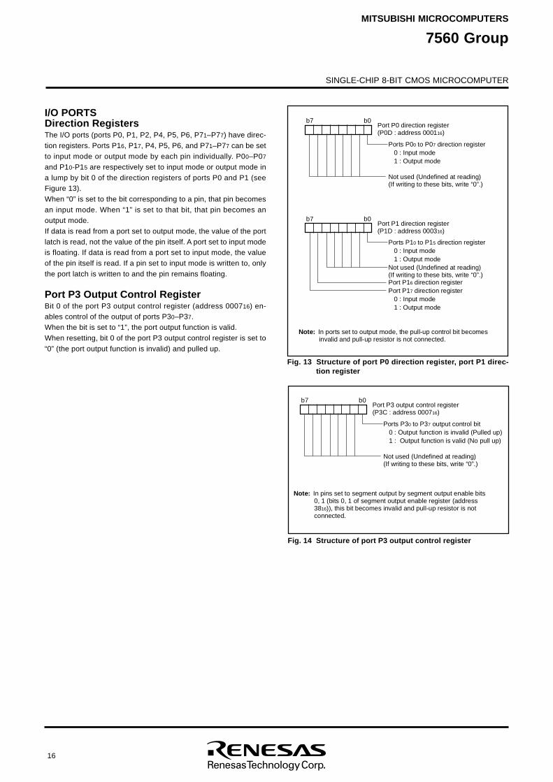
I/O PORTSDirection RegistersThe I/O ports (ports P0, P1, P2, P4, P5, P6, P71–P77) have direc-tion registers. Ports P16, P17, P4, P5, P6, and P71–P77 can be setto input mode or output mode by each pin individually. P00–P07
and P10-P15 are respectively set to input mode or output mode ina lump by bit 0 of the direction registers of ports P0 and P1 (seeFigure 13).When “0” is set to the bit corresponding to a pin, that pin becomesan input mode. When “1” is set to that bit, that pin becomes anoutput mode.If data is read from a port set to output mode, the value of the portlatch is read, not the value of the pin itself. A port set to input modeis floating. If data is read from a port set to input mode, the valueof the pin itself is read. If a pin set to input mode is written to, onlythe port latch is written to and the pin remains floating.
Port P3 Output Control RegisterBit 0 of the port P3 output control register (address 000716) en-ables control of the output of ports P30–P37.When the bit is set to “1”, the port output function is valid.When resetting, bit 0 of the port P3 output control register is set to“0” (the port output function is invalid) and pulled up.
Fig. 13 Structure of port P0 direction register, port P1 direc-tion register
Fig. 14 Structure of port P3 output control register
Ports P00 to P07 direction register0 : Input mode1 : Output mode
Not used (Undefined at reading)(If writing to these bits, write “0”.)
Port P0 direction register(P0D : address 000116)
b
7 b0
Note: In ports set to output mode, the pull-up control bit becomes invalid and pull-up resistor is not connected.
Ports P10 to P15 direction register0 : Input mode1 : Output mode
Not used (Undefined at reading)(If writing to these bits, write “0”.)Port P16 direction registerPort P17 direction register
0 : Input mode1 : Output mode
Port P1 direction register(P1D : address 000316)
b
7 b0
Ports P30 to P37 output control bit0 : Output function is invalid (Pulled up)1 : Output function is valid (No pull up)
Not used (Undefined at reading)(If writing to these bits, write “0”.)
Port P3 output control register(P3C : address 000716)
b7 b0
N
o
t
e
: I
n
p
i
n
s
s
e
t
t
o
s
e
g
m
e
n
t
o
u
t
p
u
t
b
y
s
e
g
m
e
n
t
o
u
t
p
u
t
e
n
a
b
l
e
b
i
t
s
0
,
1
(
b
i
t
s
0
,
1
o
f
s
e
g
m
e
n
t
o
u
t
p
u
t
e
n
a
b
l
e
r
e
g
i
s
t
e
r
(
a
d
d
r
e
s
s
3
81
6)
)
,
t
h
i
s
b
i
t
b
e
c
o
m
e
s
i
n
v
a
l
i
d
a
n
d
p
u
l
l
-
u
p
r
e
s
i
s
t
o
r
i
s
n
o
t
c
o
n
n
e
c
t
e
d
.
SINGLE-CHIP 8-BIT CMOS MICROCOMPUTER
MITSUBISHI MICROCOMPUTERS
7560 Group
17
Fig. 15 Structure of PULL register A and PULL register B
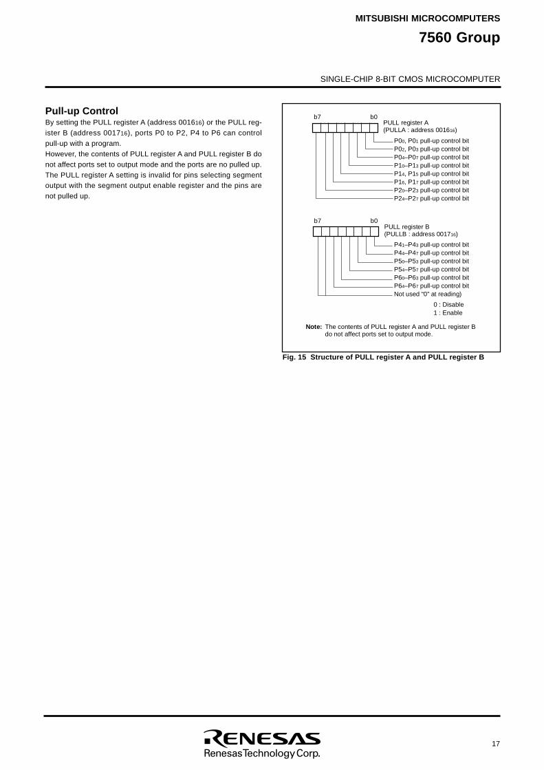
Pull-up ControlBy setting the PULL register A (address 001616) or the PULL reg-ister B (address 001716), ports P0 to P2, P4 to P6 can controlpull-up with a program.However, the contents of PULL register A and PULL register B donot affect ports set to output mode and the ports are no pulled up.The PULL register A setting is invalid for pins selecting segmentoutput with the segment output enable register and the pins arenot pulled up.
P00, P01 pull-up control bitP02, P03 pull-up control bitP04–P07 pull-up control bitP10–P13 pull-up control bitP14, P15 pull-up control bitP16, P17 pull-up control bitP20–P23 pull-up control bitP24–P27 pull-up control bit
P
U
L
L
r
e
g
i
s
t
e
r
A(
P
U
L
L
A
:
a
d
d
r
e
s
s
0
0
1
61
6)
b
7 b
0
P41–P43 pull-up control bitP44–P47 pull-up control bitP50–P53 pull-up control bitP54–P57 pull-up control bitP60–P63 pull-up control bitP64–P67 pull-up control bitNot used “0” at reading)
0
:
D
i
s
a
b
l
e1
:
E
n
a
b
l
e
P
U
L
L
r
e
g
i
s
t
e
r
B(
P
U
L
L
B
:
a
d
d
r
e
s
s
0
0
1
71
6)
b7 b
0
Note: The contents of PULL register A and PULL register B do not affect ports set to output mode.
SINGLE-CHIP 8-BIT CMOS MICROCOMPUTER
MITSUBISHI MICROCOMPUTERS
7560 Group
18
PWM output
DA2 output
A-D external triggerinput
DA1 output
Diagram No.Related SFRsInput/OutputNamePin Non-Port FunctionI/O Format
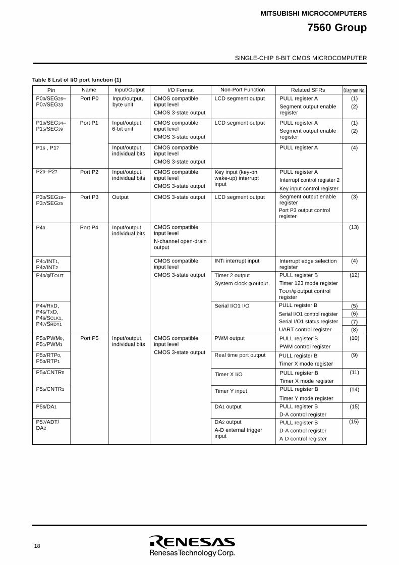
Table 8 List of I/O port function (1)
P00/SEG26–P07/SEG33
P10/SEG34–P15/SEG39
P16 , P17
P20–P27
P30/SEG18–P37/SEG25
P40
P41/INT1,P42/INT2
P43/φ/TOUT
P44/RXD,P45/TXD,P46/SCLK1,P47/SRDY1
P50/PWM0,P51/PWM1
P52/RTP0,P53/RTP1
P54/CNTR0
P55/CNTR1
P56/DA1
P57/ADT/DA2
Port P0
Port P1
Port P2
Port P3
Port P4
Port P5
Input/output,byte unit
Input/output,6-bit unit
Input/output,individual bits
Input/output,individual bits
Output
Input/output,individual bits
Input/output,individual bits
CMOS compatibleinput level
CMOS 3-state output
CMOS compatibleinput level
CMOS 3-state output
CMOS compatibleinput level
CMOS 3-state output
CMOS compatibleinput level
CMOS 3-state output
CMOS 3-state output
CMOS compatibleinput level
N-channel open-drainoutput
CMOS compatibleinput level
CMOS 3-state output
CMOS compatibleinput level
CMOS 3-state output
LCD segment output
LCD segment output
Key input (key-onwake-up) interruptinput
LCD segment output
INTi interrupt input
Timer 2 output
System clock φ output
Serial I/O1 I/O
Real time port output
Timer X I/O
Timer Y input
PULL register A
Segment output enableregister
PULL register A
Segment output enableregister
PULL register A
PULL register A
Interrupt control register 2
Key input control register
Segment output enableregister
Interrupt edge selectionregister
PULL register B
Timer 123 mode register
TOUT/φ output controlregister
PULL register B
Serial I/O1 control registerSerial I/O1 status register
UART control register
PULL register B
PWM control register
PULL register B
Timer X mode register
PULL register B
Timer X mode register
PULL register B
Timer Y mode register
PULL register B
D-A control register
PULL register B
D-A control register
A-D control register
(1)
(2)
(1)
(2)
(4)
(3)
(13)
(4)
(12)
(5)(6)
(7)
(8)
(10)
(9)
(11)
(14)
(15)
(15)
Port P3 output controlregister
SINGLE-CHIP 8-BIT CMOS MICROCOMPUTER
MITSUBISHI MICROCOMPUTERS
7560 Group
19
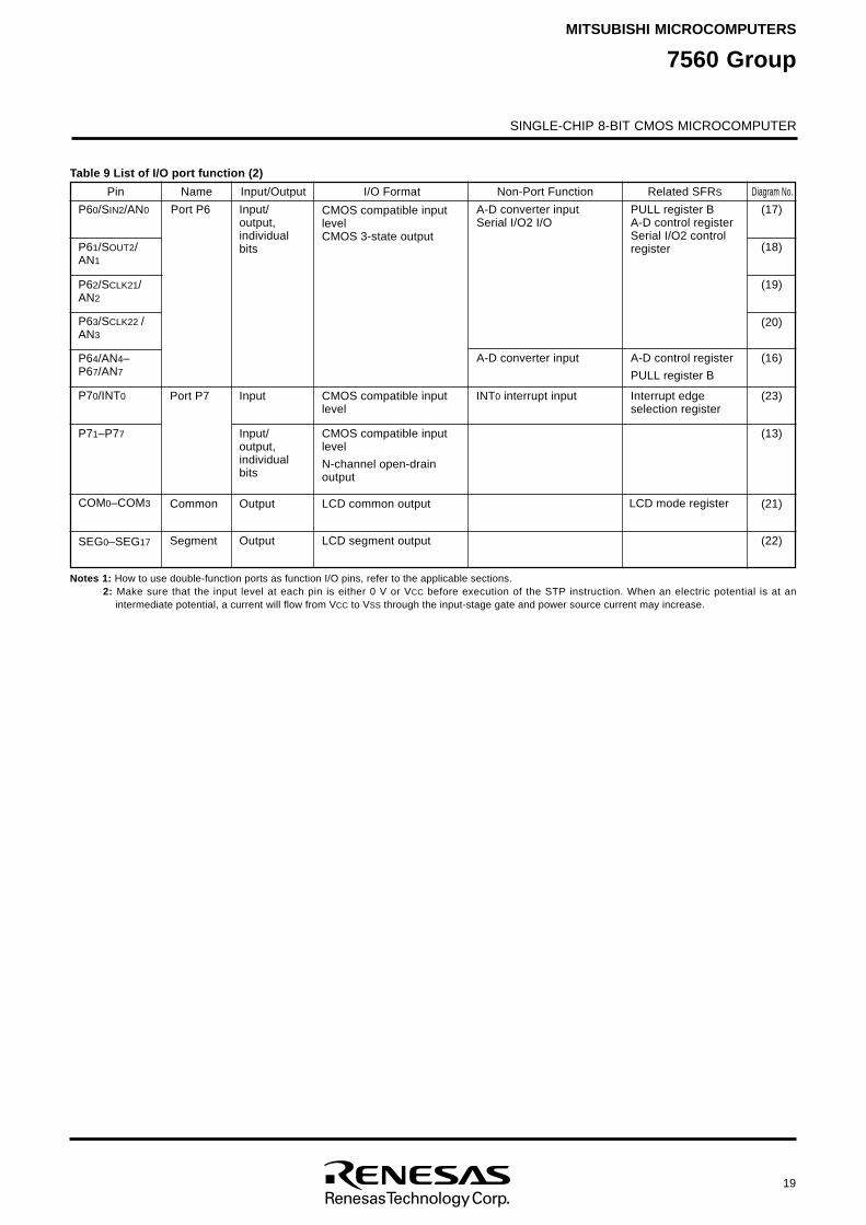
Pin Name I/O Format Non-Port Function Related SFRS Diagram No.Input/Output
Notes 1: How to use double-function ports as function I/O pins, refer to the applicable sections.2: Make sure that the input level at each pin is either 0 V or VCC before execution of the STP instruction. When an electric potential is at an
intermediate potential, a current will flow from VCC to VSS through the input-stage gate and power source current may increase.
Table 9 List of I/O port function (2)
P60/SIN2/AN0
P61/SOUT2/AN1
P62/SCLK21/AN2
P63/SCLK22 /AN3
P64/AN4–P67/AN7
P70/INT0
P71–P77
COM0–COM3
SEG0–SEG17
Port P6
Port P7
Common
Segment
Input/output,individualbits
Input
Input/output,individualbits
Output
Output
CMOS compatible inputlevelCMOS 3-state output
CMOS compatible inputlevel
CMOS compatible inputlevel
N-channel open-drainoutput
LCD common output
LCD segment output
A-D converter inputSerial I/O2 I/O
A-D converter input
INT0 interrupt input
PULL register BA-D control registerSerial I/O2 controlregister
A-D control register
PULL register B
Interrupt edgeselection register
(17)
(18)
(19)
(20)
(16)
(23)
(13)
(21)
(22)
LCD mode register
SINGLE-CHIP 8-BIT CMOS MICROCOMPUTER
MITSUBISHI MICROCOMPUTERS
7560 Group
20
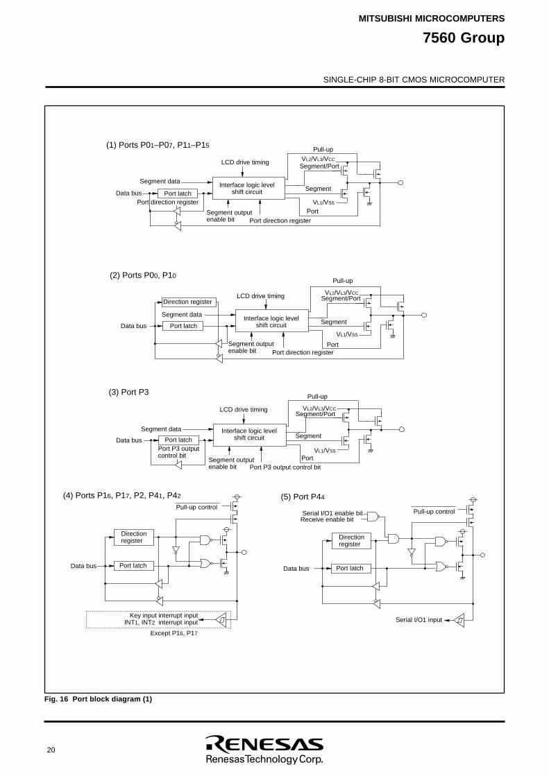
Fig. 16 Port block diagram (1)
(5) Port P44( 4
)
P
o
r
t
s
P
16,
P
17,
P
2
,
P
41,
P
42
Pull-up control
VL
1/
VS
S
VL2/VL3/VCC
VL1/VSS
VL
2/
VL
3/
VC
C
VL1/VSS
VL
2/
VL
3/
VC
C
( 1
)
P
o
r
t
s
P
01–
P
07,
P
11–
P
15
D
a
t
a
b
u
s P
o
r
t
l
a
t
c
hI
n
t
e
r
f
a
c
e
l
o
g
i
c
l
e
v
e
l
s
h
i
f
t
c
i
r
c
u
i
t
P
u
l
l
-
u
p
P
o
r
t
S
e
g
m
e
n
t
S
e
g
m
e
n
t
/
P
o
r
tL C
D
d
r
i
v
e
t
i
m
i
n
g
S
e
g
m
e
n
t
o
u
t
p
u
t
e
n
a
b
l
e
b
i
t
S
e
g
m
e
n
t
d
a
t
a
Port direction register
P
o
r
t
d
i
r
e
c
t
i
o
n
r
e
g
i
s
t
e
r
( 2
)
P
o
r
t
s
P
00,
P
10
D
a
t
a
b
u
s P
o
r
t
l
a
t
c
hInterface logic level
shift circuit
Port
S
e
g
m
e
n
t
Segment/PortLCD drive timing
S
e
g
m
e
n
t
d
a
t
a
Port direction register
D
i
r
e
c
t
i
o
n
r
e
g
i
s
t
e
r
Pull-up
D
a
t
a
b
u
s Port latchI
n
t
e
r
f
a
c
e
l
o
g
i
c
l
e
v
e
l
s
h
i
f
t
c
i
r
c
u
i
t
P
o
r
t
S
e
g
m
e
n
t
Segment/PortLCD drive timing
Segment data
P
o
r
t
P
3
ou
t
p
u
t
c
o
n
t
r
o
l
b
i
t
Pull-up( 3
)
P
o
r
t
P
3
D
a
t
a
b
u
s Port latch
D
i
r
e
c
t
i
o
n
r
e
g
i
s
t
e
r
Key input interrupt inputINT1, INT2 interrupt input
E
x
c
e
p
t
P
16,
P
17
P
u
l
l
-
u
p
c
o
n
t
r
o
l
Data bus Port latch
D
i
r
e
c
t
i
o
n
r
e
g
i
s
t
e
r
S
e
r
i
a
l
I
/
O
1
e
n
a
b
l
e
b
i
t
S
e
r
i
a
l
I
/
O
1
i
n
p
u
t
R
e
c
e
i
v
e
e
n
a
b
l
e
b
i
t
S
e
g
m
e
n
t
o
u
t
p
u
t
e
n
a
b
l
e
b
i
t
S
e
g
m
e
n
t
o
u
t
p
u
t
e
n
a
b
l
e
b
i
t
Port P3 output control bit
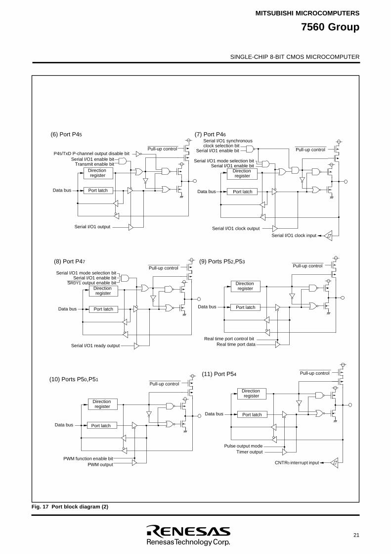
SINGLE-CHIP 8-BIT CMOS MICROCOMPUTER
MITSUBISHI MICROCOMPUTERS
7560 Group
21
Fig. 17 Port block diagram (2)
(6) Port P45 (7) Port P46
(8) Port P47 (9) Ports P52,P53
( 1
0
)
P
o
r
t
s
P
50,
P
51
P
W
M
f
u
n
c
t
i
o
n
e
n
a
b
l
e
b
i
tP
W
M
o
u
t
p
u
t
( 1
1
)
P
o
r
t
P
54
Pulse output modeTimer output
CNTR0 interrupt input
P
u
l
l
-
u
p
c
o
n
t
r
o
l
D
i
r
e
c
t
i
o
n
r
e
g
i
s
t
e
r
D
a
t
a
b
u
s P
o
r
t
l
a
t
c
h
S
e
r
i
a
l
I
/
O
1
o
u
t
p
u
t
P
45/
T
x
D
P
-
c
h
a
n
n
e
l
o
u
t
p
u
t
d
i
s
a
b
l
e
b
i
tS
e
r
i
a
l
I
/
O
1
e
n
a
b
l
e
b
i
t
T
r
a
n
s
m
i
t
e
n
a
b
l
e
b
i
t
Serial I/O1 clock output
D
i
r
e
c
t
i
o
n
r
e
g
i
s
t
e
r
Data bus P
o
r
t
l
a
t
c
h
P
u
l
l
-
u
p
c
o
n
t
r
o
lS
e
r
i
a
l
I
/
O
1
e
n
a
b
l
e
b
i
t
S
e
r
i
a
l
I
/
O
1
c
l
o
c
k
i
n
p
u
t
Serial I/O1 synchronous clock selection bit
Serial I/O1 mode selection bitSerial I/O1 enable bit
P
u
l
l
-
u
p
c
o
n
t
r
o
lS
e
r
i
a
l
I
/
O
1
m
o
d
e
s
e
l
e
c
t
i
o
n
b
i
t
S
e
r
i
a
l
I
/
O
1
e
n
a
b
l
e
b
i
tSR
D
Y
1
o
u
t
p
u
t
e
n
a
b
l
e
b
i
tD
i
r
e
c
t
i
o
n
r
e
g
i
s
t
e
r
Data bus Port latch
Serial I/O1 ready output
D
i
r
e
c
t
i
o
n
r
e
g
i
s
t
e
r
Data bus Port latch
Pull-up control
Real time port control bitReal time port data
P
u
l
l
-
u
p
c
o
n
t
r
o
l
Direction register
Data bus Port latch
P
u
l
l
-
u
p
c
o
n
t
r
o
l
D
i
r
e
c
t
i
o
n
r
e
g
i
s
t
e
r
D
a
t
a
b
u
s P
o
r
t
l
a
t
c
h
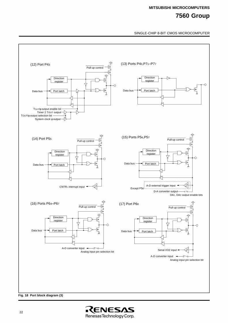
SINGLE-CHIP 8-BIT CMOS MICROCOMPUTER
MITSUBISHI MICROCOMPUTERS
7560 Group
22
Fig. 18 Port block diagram (3)
(12) Port P43
TOUT/φ output enable bitTimer 2 TOUT output
System clock φ outputTOUT/φ output selection bit
(13) Ports P40,P71–P77
(14) Port P55
CNTR1 interrupt input
(15) Ports P56,P57
A-D external trigger input
D-A converter outputExcept P56
(16) Ports P64–P67 (17) Port P60
Analog input pin selection bitA-D converter input
Serial I/O2 input
DA1, DA2 output enable bits
Direction register
Port latchData bus
Pull-up control
Direction register
Port latchData bus
Direction register
Port latchData bus
Pull-up control
Direction register
Port latchData bus
Pull-up control
Direction register
Port latchData bus
Pull-up control
Analog input pin selection bitA-D converter input
Direction register
Port latchData bus
Pull-up control
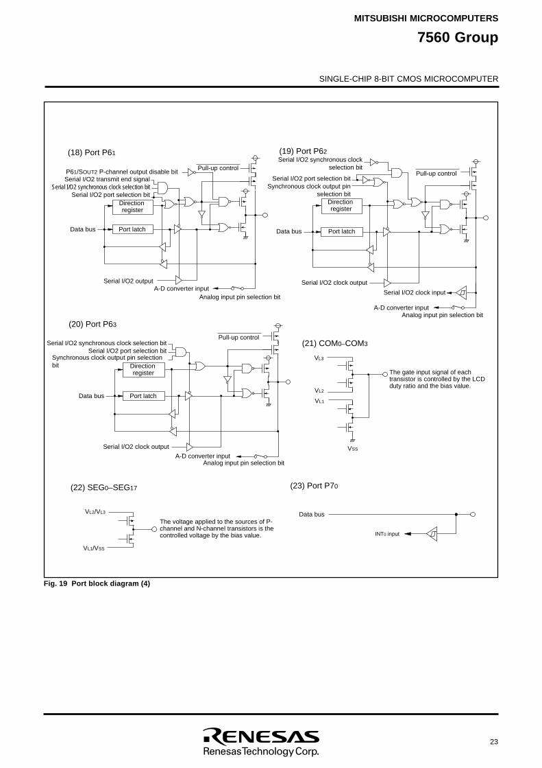
SINGLE-CHIP 8-BIT CMOS MICROCOMPUTER
MITSUBISHI MICROCOMPUTERS
7560 Group
23
Fig. 19 Port block diagram (4)
(18) Port P61 (19) Port P62
( 2
0
)
P
o
r
t
P
63
S
e
r
i
a
l
I
/
O
2
o
u
t
p
u
t
Serial I/O2 transmit end signalSerial I/O2 synchronous clock selection bit
Serial I/O2 port selection bit
P
u
l
l
-
u
p
c
o
n
t
r
o
l
A
n
a
l
o
g
i
n
p
u
t
p
i
n
s
e
l
e
c
t
i
o
n
b
i
tA
-
D
c
o
n
v
e
r
t
e
r
i
n
p
u
t
P
61/
SO
U
T
2
P
-
c
h
a
n
n
e
l
o
u
t
p
u
t
d
i
s
a
b
l
e
b
i
t
( 2
1
)
C
O
M0
–C
O
M3
( 2
2
)
S
E
G0–
S
E
G1
7
VL3
VL2
VL1
VSS
VL
2/
VL
3
VL1/VSS
(23) Port P70
I N
T0
i
n
p
u
t
Serial I/O2 synchronous clockselection bit
Serial I/O2 clock output
S
e
r
i
a
l
I
/
O
2
c
l
o
c
k
i
n
p
u
t
S
e
r
i
a
l
I
/
O
2
p
o
r
t
s
e
l
e
c
t
i
o
n
b
i
tS
y
n
c
h
r
o
n
o
u
s
c
l
o
c
k
o
u
t
p
u
t
p
i
ns
e
l
e
c
t
i
o
n
b
i
t
A-D converter input
S
e
r
i
a
l
I
/
O
2
c
l
o
c
k
o
u
t
p
u
t
A-D converter input
D
i
r
e
c
t
i
o
n
r
e
g
i
s
t
e
r
P
o
r
t
l
a
t
c
hD
a
t
a
b
u
s
P
u
l
l
-
u
p
c
o
n
t
r
o
l
Direction register
P
o
r
t
l
a
t
c
hD
a
t
a
b
u
s
Analog input pin selection bit
Pull-up control
D
i
r
e
c
t
i
o
n
r
e
g
i
s
t
e
r
P
o
r
t
l
a
t
c
hData bus
Analog input pin selection bit
Serial I/O2 synchronous clock selection bitSerial I/O2 port selection bit
Data bus
T
h
e
g
a
t
e
i
n
p
u
t
s
i
g
n
a
l
o
f
e
a
c
h
t
r
a
n
s
i
s
t
o
r
i
s
c
o
n
t
r
o
l
l
e
d
b
y
t
h
e
L
C
D
d
u
t
y
r
a
t
i
o
a
n
d
t
h
e
b
i
a
s
v
a
l
u
e
.
T
h
e
v
o
l
t
a
g
e
a
p
p
l
i
e
d
t
o
t
h
e
s
o
u
r
c
e
s
o
f
P
-c
h
a
n
n
e
l
a
n
d
N
-
c
h
a
n
n
e
l
t
r
a
n
s
i
s
t
o
r
s
i
s
t
h
e
c
o
n
t
r
o
l
l
e
d
v
o
l
t
a
g
e
b
y
t
h
e
b
i
a
s
v
a
l
u
e
.
Synchronous clock output pin selection bit
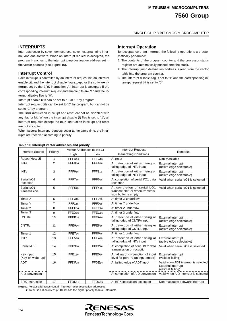
SINGLE-CHIP 8-BIT CMOS MICROCOMPUTER
MITSUBISHI MICROCOMPUTERS
7560 Group
24
INTERRUPTSInterrupts occur by seventeen sources: seven external, nine inter-nal, and one software. When an interrupt request is accepted, theprogram branches to the interrupt jump destination address set inthe vector address (see Figure 10).
Interrupt ControlEach interrupt is controlled by an interrupt request bit, an interruptenable bit, and the interrupt disable flag except for the software in-terrupt set by the BRK instruction. An interrupt is accepted if thecorresponding interrupt request and enable bits are “1” and the in-terrupt disable flag is “0”.Interrupt enable bits can be set to “0” or “1” by program.Interrupt request bits can be set to “0” by program, but cannot beset to “1” by program.The BRK instruction interrupt and reset cannot be disabled withany flag or bit. When the interrupt disable (I) flag is set to “1”, allinterrupt requests except the BRK instruction interrupt and resetare not accepted.When several interrupt requests occur at the same time, the inter-rupts are received according to priority.
Interrupt OperationBy acceptance of an interrupt, the following operations are auto-matically performed:1. The contents of the program counter and the processor status
register are automatically pushed onto the stack.2. The interrupt jump destination address is read from the vector
table into the program counter.3. The interrupt disable flag is set to “1” and the corresponding in-
terrupt request bit is set to “0”.
Notes1: Vector addresses contain interrupt jump destination addresses.2: Reset is not an interrupt. Reset has the higher priority than all interrupts.
Table 10 Interrupt vector addresses and priority
RemarksInterrupt Request
Generating Conditions
At reset
At detection of either rising orfalling edge of INT0 input
At detection of either rising orfalling edge of INT1 input
At completion of serial I/O1 datareception
At completion of serial I/O1transmit shift or when transmis-sion buffer is empty
Interrupt SourceLowHigh
PriorityVector Addresses (Note 1)
Reset (Note 2)INT0
INT1
Serial I/O1reception
Serial I/O1transmission
Timer X
Timer Y
Timer 2Timer 3
CNTR0
CNTR1
Timer 1
INT2
Serial I/O2
Key input(Key-on wake-up)
ADT
A-D conversion
BRK instruction
12
3
4
5
6
7
8
9
10
11
12
13
14
15
16
17
FFFD16
FFFB16
FFF916
FFF716
FFF516
FFF316
FFF116
FFEF16
FFED16
FFEB16
FFE916
FFE716
FFE516
FFE316
FFE116
FFDF16
FFDD16
FFFC16
FFFA16
FFF816
FFF616
FFF416
FFF216
FFF016
FFEE16
FFEC16
FFEA16
FFE816
FFE616
FFE416
FFE216
FFE016
FFDE16
FFDC16
At timer X underflow
At timer Y underflow
At timer 2 underflow
At timer 3 underflow
At detection of either rising orfalling edge of CNTR0 input
At detection of either rising orfalling edge of CNTR1 input
At timer 1 underflow
At detection of either rising orfalling edge of INT2 input
At completion of serial I/O2 datatransmission or reception
At falling of conjunction of inputlevel for port P2 (at input mode)
At falling edge of ADT input
At completion of A-D conversion
At BRK instruction execution
Non-maskable
External interrupt(active edge selectable)
External interrupt(active edge selectable)
Valid when serial I/O1 is selected
Valid when serial I/O1 is selected
External interrupt(active edge selectable)
External interrupt(active edge selectable)
External interrupt(active edge selectable)
Valid when serial I/O2 is selected
External interrupt(valid at falling)
Valid when ADT interrupt is selectedExternal interrupt(valid at falling)
Valid when A-D interrupt is selected
Non-maskable software interrupt
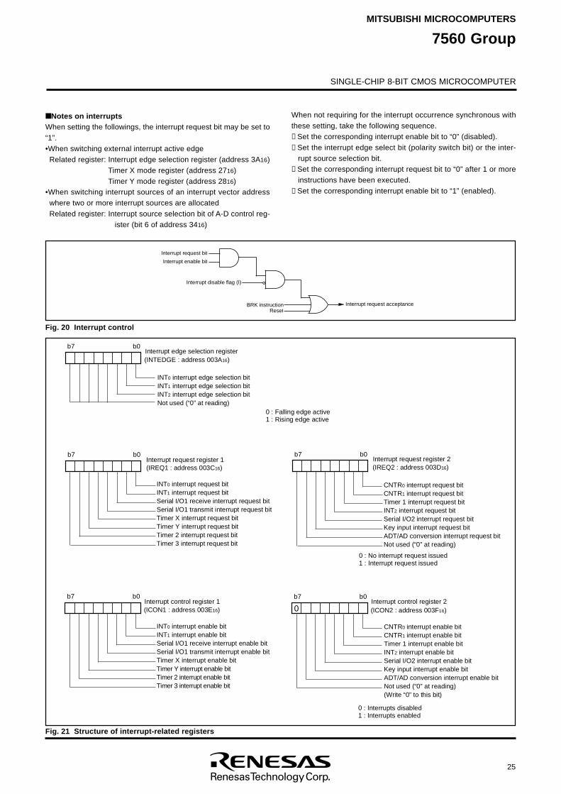
SINGLE-CHIP 8-BIT CMOS MICROCOMPUTER
MITSUBISHI MICROCOMPUTERS
7560 Group
25
Fig. 20 Interrupt control
Fig. 21 Structure of interrupt-related registers
Notes on interruptsWhen setting the followings, the interrupt request bit may be set to“1”.•When switching external interrupt active edgeRelated register: Interrupt edge selection register (address 3A16)
Timer X mode register (address 2716)Timer Y mode register (address 2816)
•When switching interrupt sources of an interrupt vector addresswhere two or more interrupt sources are allocatedRelated register: Interrupt source selection bit of A-D control reg-
ister (bit 6 of address 3416)
When not requiring for the interrupt occurrence synchronous withthese setting, take the following sequence.➀ Set the corresponding interrupt enable bit to “0” (disabled).➁ Set the interrupt edge select bit (polarity switch bit) or the inter-
rupt source selection bit.➂ Set the corresponding interrupt request bit to “0” after 1 or more
instructions have been executed.➃ Set the corresponding interrupt enable bit to “1” (enabled).
I
n
t
e
r
r
u
p
t
r
e
q
u
e
s
t
b
i
t
I
n
t
e
r
r
u
p
t
e
n
a
b
l
e
b
i
t
I
n
t
e
r
r
u
p
t
d
i
s
a
b
l
e
f
l
a
g
(
I
)
BRK instructionReset
Interrupt request acceptance
b7 b0I n
t
e
r
r
u
p
t
e
d
g
e
s
e
l
e
c
t
i
o
n
r
e
g
i
s
t
e
r
I N
T0
i
n
t
e
r
r
u
p
t
e
d
g
e
s
e
l
e
c
t
i
o
n
b
i
t
I
N
T1
i
n
t
e
r
r
u
p
t
e
d
g
e
s
e
l
e
c
t
i
o
n
b
i
tI
N
T2
i
n
t
e
r
r
u
p
t
e
d
g
e
s
e
l
e
c
t
i
o
n
b
i
tN
o
t
u
s
e
d
(
“
0
”
a
t
r
e
a
d
i
n
g
)
(INTEDGE : address 003A16)
I n
t
e
r
r
u
p
t
r
e
q
u
e
s
t
r
e
g
i
s
t
e
r
1
I N
T0
i
n
t
e
r
r
u
p
t
r
e
q
u
e
s
t
b
i
t
I
N
T1
i
n
t
e
r
r
u
p
t
r
e
q
u
e
s
t
b
i
tS
e
r
i
a
l
I
/
O
1
r
e
c
e
i
v
e
i
n
t
e
r
r
u
p
t
r
e
q
u
e
s
t
b
i
t
S
e
r
i
a
l
I
/
O
1
t
r
a
n
s
m
i
t
i
n
t
e
r
r
u
p
t
r
e
q
u
e
s
t
b
i
tT
i
m
e
r
X
i
n
t
e
r
r
u
p
t
r
e
q
u
e
s
t
b
i
tT
i
m
e
r
Y
i
n
t
e
r
r
u
p
t
r
e
q
u
e
s
t
b
i
tT
i
m
e
r
2
i
n
t
e
r
r
u
p
t
r
e
q
u
e
s
t
b
i
tT
i
m
e
r
3
i
n
t
e
r
r
u
p
t
r
e
q
u
e
s
t
b
i
t
I n
t
e
r
r
u
p
t
c
o
n
t
r
o
l
r
e
g
i
s
t
e
r
1
I N
T0
i
n
t
e
r
r
u
p
t
e
n
a
b
l
e
b
i
t
I
N
T1
i
n
t
e
r
r
u
p
t
e
n
a
b
l
e
b
i
tS
e
r
i
a
l
I
/
O
1
r
e
c
e
i
v
e
i
n
t
e
r
r
u
p
t
e
n
a
b
l
e
b
i
tS
e
r
i
a
l
I
/
O
1
t
r
a
n
s
m
i
t
i
n
t
e
r
r
u
p
t
e
n
a
b
l
e
b
i
tT
i
m
e
r
X
i
n
t
e
r
r
u
p
t
e
n
a
b
l
e
b
i
tT
i
m
e
r
Y
i
n
t
e
r
r
u
p
t
e
n
a
b
l
e
b
i
tT
i
m
e
r
2
i
n
t
e
r
r
u
p
t
e
n
a
b
l
e
b
i
tT
i
m
e
r
3
i
n
t
e
r
r
u
p
t
e
n
a
b
l
e
b
i
t
0
:
N
o
i
n
t
e
r
r
u
p
t
r
e
q
u
e
s
t
i
s
s
u
e
d1
:
I
n
t
e
r
r
u
p
t
r
e
q
u
e
s
t
i
s
s
u
e
d
( I
R
E
Q
1
:
a
d
d
r
e
s
s
0
0
3
C1
6)
( I
C
O
N
1
:
a
d
d
r
e
s
s
0
0
3
E1
6)
I n
t
e
r
r
u
p
t
r
e
q
u
e
s
t
r
e
g
i
s
t
e
r
2
CNTR0 interrupt request bitCNTR1 interrupt request bitTimer 1 interrupt request bitINT2 interrupt request bitSerial I/O2 interrupt request bit Key input interrupt request bitADT/AD conversion interrupt request bitNot used (“0” at reading)
( I
R
E
Q
2
:
a
d
d
r
e
s
s
0
0
3
D1
6)
Interrupt control register 2
CNTR0 interrupt enable bitCNTR1 interrupt enable bitTimer 1 interrupt enable bitINT2 interrupt enable bitSerial I/O2 interrupt enable bit Key input interrupt enable bitADT/AD conversion interrupt enable bitNot used (“0” at reading)(Write “0” to this bit)
0 : Interrupts disabled1 : Interrupts enabled
(ICON2 : address 003F16)
0 : Falling edge active1 : Rising edge active
b
7 b
0
b
7 b
0
b7 b0
b
7 b0
0
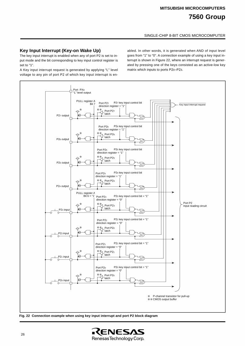
SINGLE-CHIP 8-BIT CMOS MICROCOMPUTER
MITSUBISHI MICROCOMPUTERS
7560 Group
26
Key Input Interrupt (Key-on Wake Up)The key input interrupt is enabled when any of port P2 is set to in-put mode and the bit corresponding to key input control register isset to “1”.A Key input interrupt request is generated by applying “L” levelvoltage to any pin of port P2 of which key input interrupt is en-
abled. In other words, it is generated when AND of input levelgoes from “1” to “0”. A connection example of using a key input in-terrupt is shown in Figure 22, where an interrupt request is gener-ated by pressing one of the keys consisted as an active-low keymatrix which inputs to ports P20–P23.
Fig. 22 Connection example when using key input interrupt and port P2 block diagram
P
o
r
t
P
20l
a
t
c
h
P
o
r
t
P
20d
i
r
e
c
t
i
o
n
r
e
g
i
s
t
e
r
=
“
0
”
P
o
r
t
P
21l
a
t
c
h
Port P21direction register = “0”
P
o
r
t
P
22l
a
t
c
h
Port P22direction register = “0”
Port P23latch
Port P23direction register = “0”
Port P24latch
Port P24direction register = “1”
Port P25latch
Port P25direction register = “1”
P
o
r
t
P
26l
a
t
c
h
P
o
r
t
P
26d
i
r
e
c
t
i
o
n
r
e
g
i
s
t
e
r
=
“
1
”
Port P27latch
Port P27direction register = “1”
P
20
i
n
p
u
t
P21 input
P22 input
P
23
i
n
p
u
t
P
24
o
u
t
p
u
t
P
25
o
u
t
p
u
t
P
26
o
u
t
p
u
t
P
27
o
u
t
p
u
t
P
U
L
L
r
e
g
i
s
t
e
r
AB
i
t
7
Port P2Input reading circuit
P
o
r
t
P
X
x“
L
”
l
e
v
e
l
o
u
t
p
u
t
P-channel transistor for pull-up CMOS output buffer
K
e
y
i
n
p
u
t
i
n
t
e
r
r
u
p
t
r
e
q
u
e
s
t
P27 key input control bit
P
26
k
e
y
i
n
p
u
t
c
o
n
t
r
o
l
b
i
t
P
25
k
e
y
i
n
p
u
t
c
o
n
t
r
o
l
b
i
t
P
24
k
e
y
i
n
p
u
t
c
o
n
t
r
o
l
b
i
t
P
23
k
e
y
i
n
p
u
t
c
o
n
t
r
o
l
b
i
t
=
“
1
”P
U
L
L
r
e
g
i
s
t
e
r
A
B
i
t
6
=
“
1
”
P
22
k
e
y
i
n
p
u
t
c
o
n
t
r
o
l
b
i
t
=
“
1
”
P
21
k
e
y
i
n
p
u
t
c
o
n
t
r
o
l
b
i
t
=
“
1
”
P20 key input control bit = “1”
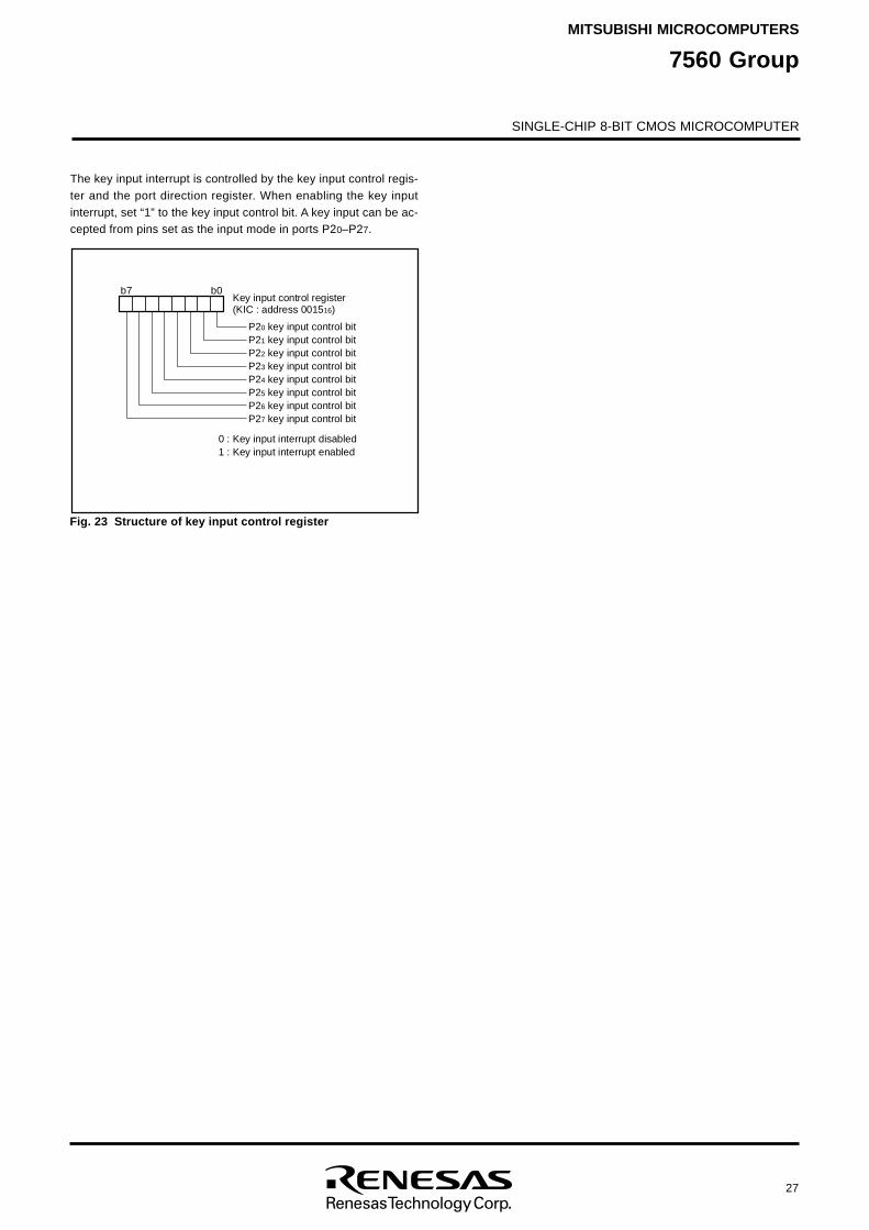
SINGLE-CHIP 8-BIT CMOS MICROCOMPUTER
MITSUBISHI MICROCOMPUTERS
7560 Group
27
The key input interrupt is controlled by the key input control regis-ter and the port direction register. When enabling the key inputinterrupt, set “1” to the key input control bit. A key input can be ac-cepted from pins set as the input mode in ports P20–P27.
Fig. 23 Structure of key input control register
P20 key input control bitP21 key input control bitP22 key input control bitP23 key input control bitP24 key input control bitP25 key input control bitP26 key input control bitP27 key input control bit
0
:
K
e
y
i
n
p
u
t
i
n
t
e
r
r
u
p
t
d
i
s
a
b
l
e
d1
:
K
e
y
i
n
p
u
t
i
n
t
e
r
r
u
p
t
e
n
a
b
l
e
d
Key input control register(KIC : address 001516)
b
7 b
0
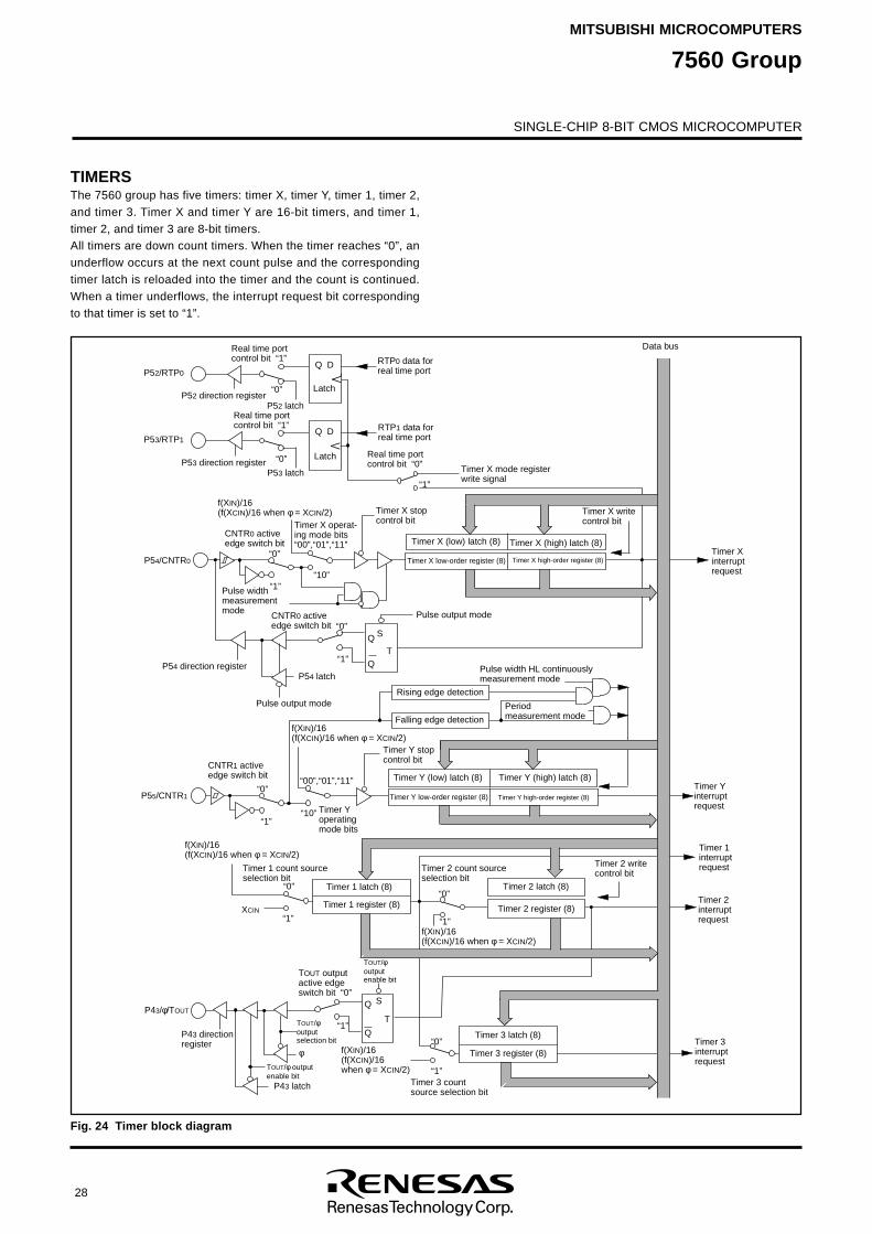
SINGLE-CHIP 8-BIT CMOS MICROCOMPUTER
MITSUBISHI MICROCOMPUTERS
7560 Group
28
TIMERSThe 7560 group has five timers: timer X, timer Y, timer 1, timer 2,and timer 3. Timer X and timer Y are 16-bit timers, and timer 1,timer 2, and timer 3 are 8-bit timers.All timers are down count timers. When the timer reaches “0”, anunderflow occurs at the next count pulse and the correspondingtimer latch is reloaded into the timer and the count is continued.When a timer underflows, the interrupt request bit correspondingto that timer is set to “1”.
Fig. 24 Timer block diagram
“1”
P55/CNTR1“0”
“ 1
0
”
“00”,“01”,“11”
P54/CNTR0
Q
QT
S“0”
“1”
“ 0
”
Q
D
“ 0
”
Q
D
“ 1
”
“ 0
”
“1”“ 1
0
”
Q
T
S
“ 0
”
“ 1
”
“0”
“1”“1”
P43/φ/TOUT
XC
I
N
“0”
“1”
CNTR0 activeedge switch bit
T
i
m
e
r
1
c
o
u
n
t
s
o
u
r
c
es
e
l
e
c
t
i
o
n
b
i
t
Real time portcontrol bit “0”
f (
XI
N)
/
1
6
(
f
(
XC
I
N)
/
1
6
w
h
e
n
φ
=
XC
I
N/
2
)
C
N
T
R1
a
c
t
i
v
ee
d
g
e
s
w
i
t
c
h
b
i
t
Timer Y stopcontrol bit
Falling edge detection
P
e
r
i
o
dm
e
a
s
u
r
e
m
e
n
t
m
o
d
e
Timer Yinterruptrequest
P
u
l
s
e
w
i
d
t
h
H
L
c
o
n
t
i
n
u
o
u
s
l
y
m
e
a
s
u
r
e
m
e
n
t
m
o
d
e
R
i
s
i
n
g
e
d
g
e
d
e
t
e
c
t
i
o
n
Timer Y operating mode bits
Timer Xinterruptrequest
T
i
m
e
r
X
m
o
d
e
r
e
g
i
s
t
e
rw
r
i
t
e
s
i
g
n
a
l
P
43
d
i
r
e
c
t
i
o
n
r
e
g
i
s
t
e
r
Pulse output mode
P
54
l
a
t
c
h
Timer X stopcontrol bit
Timer X writecontrol bit
L
a
t
c
h
T
i
m
e
r
X
o
p
e
r
a
t
-i
n
g
m
o
d
e
b
i
t
s“
0
0
”
,
“
0
1
”
,
“
1
1
”
Pulse widthmeasurement mode
C
N
T
R0
a
c
t
i
v
ee
d
g
e
s
w
i
t
c
h
b
i
t
Pulse output mode
P54 direction register
TOUT outputactive edge switch bit “0”
T
i
m
e
r
2
w
r
i
t
ec
o
n
t
r
o
l
b
i
t
Timer 3 countsource selection bit
Timer 2 interrupt request
Timer 3 interruptrequest
T
i
m
e
r
2
c
o
u
n
t
s
o
u
r
c
es
e
l
e
c
t
i
o
n
b
i
t
T
i
m
e
r
1i
n
t
e
r
r
u
p
tr
e
q
u
e
s
t
D
a
t
a
b
u
sR
e
a
l
t
i
m
e
p
o
r
t
c
o
n
t
r
o
l
b
i
t
“
1
”
R
e
a
l
t
i
m
e
p
o
r
t
c
o
n
t
r
o
l
b
i
t
“
1
”
T
i
m
e
r
3
l
a
t
c
h
(
8
)
T
i
m
e
r
3
r
e
g
i
s
t
e
r
(
8
)
Timer 1 latch (8)
Timer 1 register (8)
Timer 2 latch (8)
T
i
m
e
r
2
r
e
g
i
s
t
e
r
(
8
)
Timer X low-order register (8)
Timer X (low) latch (8) Timer X (high) latch (8)
T
i
m
e
r
Y
(
l
o
w
)
l
a
t
c
h
(
8
) T
i
m
e
r
Y
(
h
i
g
h
)
l
a
t
c
h
(
8
)
Latch
P
43
l
a
t
c
h
f(XIN)/16 (f(XCIN)/16 when φ = XCIN/2)
f(XIN)/16 (f(XCIN)/16 when φ = XCIN/2)
f(XIN)/16 (f(XCIN)/16 when φ = XCIN/2)
f(XIN)/16 (f(XCIN)/16 when φ = XCIN/2)
P
52/
R
T
P0
P
53/
R
T
P1
RTP0 data for real time port
RTP1 data for real time port
P
52
d
i
r
e
c
t
i
o
n
r
e
g
i
s
t
e
rP
52
l
a
t
c
h
P53 direction registerP
53
l
a
t
c
h
φ
Timer X high-order register (8)
Timer Y low-order register (8) T
i
m
e
r
Y
h
i
g
h
-
o
r
d
e
r
r
e
g
i
s
t
e
r
(
8
)
QTO
U
T/φ o
u
t
p
u
t
s
e
l
e
c
t
i
o
n
b
i
t
TO
U
T/φ o
u
t
p
u
t
e
n
a
b
l
e
b
i
t
TO
U
T/φ output enable bit
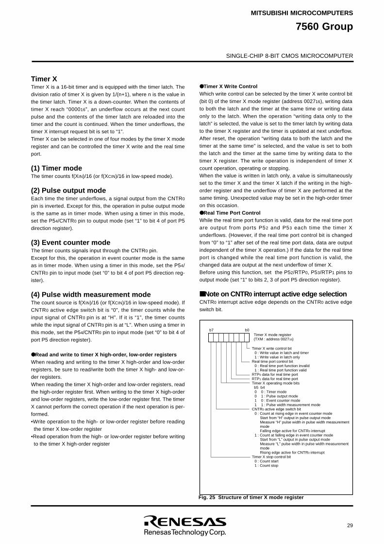
SINGLE-CHIP 8-BIT CMOS MICROCOMPUTER
MITSUBISHI MICROCOMPUTERS
7560 Group
29
Timer XTimer X is a 16-bit timer and is equipped with the timer latch. Thedivision ratio of timer X is given by 1/(n+1), where n is the value inthe timer latch. Timer X is a down-counter. When the contents oftimer X reach “000016”, an underflow occurs at the next countpulse and the contents of the timer latch are reloaded into thetimer and the count is continued. When the timer underflows, thetimer X interrupt request bit is set to “1”.Timer X can be selected in one of four modes by the timer X moderegister and can be controlled the timer X write and the real timeport.
(1) Timer modeThe timer counts f(XIN)/16 (or f(XCIN)/16 in low-speed mode).
(2) Pulse output modeEach time the timer underflows, a signal output from the CNTR0
pin is inverted. Except for this, the operation in pulse output modeis the same as in timer mode. When using a timer in this mode,set the P54/CNTR0 pin to output mode (set “1” to bit 4 of port P5direction register).
(3) Event counter modeThe timer counts signals input through the CNTR0 pin.Except for this, the operation in event counter mode is the sameas in timer mode. When using a timer in this mode, set the P54/CNTR0 pin to input mode (set “0” to bit 4 of port P5 direction reg-ister).
(4) Pulse width measurement modeThe count source is f(XIN)/16 (or f(XCIN)/16 in low-speed mode). IfCNTR0 active edge switch bit is “0”, the timer counts while theinput signal of CNTR0 pin is at “H”. If it is “1”, the timer countswhile the input signal of CNTR0 pin is at “L”. When using a timer inthis mode, set the P54/CNTR0 pin to input mode (set “0” to bit 4 ofport P5 direction register).
Read and write to timer X high-order, low-order registersWhen reading and writing to the timer X high-order and low-orderregisters, be sure to read/write both the timer X high- and low-or-der registers.When reading the timer X high-order and low-order registers, readthe high-order register first. When writing to the timer X high-orderand low-order registers, write the low-order register first. The timerX cannot perform the correct operation if the next operation is per-formed.•Write operation to the high- or low-order register before readingthe timer X low-order register
•Read operation from the high- or low-order register before writingto the timer X high-order register
Fig. 25 Structure of timer X mode register
T
i
m
e
r
X
m
o
d
e
r
e
g
i
s
t
e
r(
T
X
M
:
a
d
d
r
e
s
s
0
0
2
71
6)
Timer X write control bit0 : Write value in latch and timer1 : Write value in latch only
Real time port control bit0 : Real time port function invalid1 : Real time port function valid
RTP0 data for real time portRTP1 data for real time portTimer X operating mode bits
b5 b40 0 : Timer mode0 1 : Pulse output mode1 0 : Event counter mode1 1 : Pulse width measurement mode
CNTR0 active edge switch bit0 : Count at rising edge in event counter mode
Start from “H” output in pulse output mode Measure “H” pulse width in pulse width measurement mode Falling edge active for CNTR0 interrupt
1 : Count at falling edge in event counter mode Start from “L” output in pulse output mode Measure “L” pulse width in pulse width measurement mode Rising edge active for CNTR0 interrupt
Timer X stop control bit0 : Count start1 : Count stop
b7 b0
Timer X Write ControlWhich write control can be selected by the timer X write control bit(bit 0) of the timer X mode register (address 002716), writing datato both the latch and the timer at the same time or writing dataonly to the latch. When the operation “writing data only to thelatch” is selected, the value is set to the timer latch by writing datato the timer X register and the timer is updated at next underflow.After reset, the operation “writing data to both the latch and thetimer at the same time” is selected, and the value is set to boththe latch and the timer at the same time by writing data to thetimer X register. The write operation is independent of timer Xcount operation, operating or stopping.When the value is written in latch only, a value is simultaneouslyset to the timer X and the timer X latch if the writing in the high-order register and the underflow of timer X are performed at thesame timing. Unexpected value may be set in the high-order timeron this occasion. Real Time Port ControlWhile the real time port function is valid, data for the real time portare output from ports P52 and P53 each time the timer Xunderflows. (However, if the real time port control bit is changedfrom “0” to “1” after set of the real time port data, data are outputindependent of the timer X operation.) If the data for the real timeport is changed while the real time port function is valid, thechanged data are output at the next underflow of timer X.Before using this function, set the P52/RTP0, P53/RTP1 pins tooutput mode (set “1” to bits 2, 3 of port P5 direction register).
Note on CNTR0 interrupt active edge selectionCNTR0 interrupt active edge depends on the CNTR0 active edgeswitch bit.
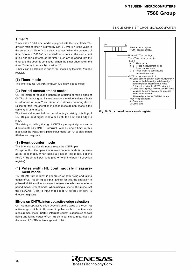
SINGLE-CHIP 8-BIT CMOS MICROCOMPUTER
MITSUBISHI MICROCOMPUTERS
7560 Group
30
Timer YTimer Y is a 16-bit timer and is equipped with the timer latch. Thedivision ratio of timer Y is given by 1/(n+1), where n is the value inthe timer latch. Timer Y is a down-counter. When the contents oftimer Y reach “000016”, an underflow occurs at the next countpulse and the contents of the timer latch are reloaded into thetimer and the count is continued. When the timer underflows, thetimer Y interrupt request bit is set to “1”.Timer Y can be selected in one of four modes by the timer Y moderegister.
(1) Timer modeThe timer counts f(XIN)/16 (or f(XCIN)/16 in low-speed mode).
(2) Period measurement modeCNTR1 interrupt request is generated at rising or falling edge ofCNTR1 pin input signal. Simultaneously, the value in timer Y latchis reloaded in timer Y and timer Y continues counting down.Except for this, the operation in period measurement mode is thesame as in timer mode.The timer value just before the reloading at rising or falling ofCNTR1 pin input signal is retained until the next valid edge isinput.The rising or falling timing of CNTR1 pin input signal can bediscriminated by CNTR1 interrupt. When using a timer in thismode, set the P55/CNTR1 pin to input mode (set “0” to bit 5 of portP5 direction register).
(3) Event counter modeThe timer counts signals input through the CNTR1 pin.Except for this, the operation in event counter mode is the sameas in timer mode. When using a timer in this mode, set theP55/CNTR1 pin to input mode (set “0” to bit 5 of port P5 directionregister).
(4) Pulse width HL continuously measure-ment mode
CNTR1 interrupt request is generated at both rising and fallingedges of CNTR1 pin input signal. Except for this, the operation inpulse width HL continuously measurement mode is the same as inperiod measurement mode. When using a timer in this mode, setthe P55/CNTR1 pin to input mode (set “0” to bit 5 of port P5direction register).
Note on CNTR1 interrupt active edge selectionCNTR1 interrupt active edge depends on the value of the CNTR1
active edge switch bit. However, in pulse width HL continuouslymeasurement mode, CNTR1 interrupt request is generated at bothrising and falling edges of CNTR1 pin input signal regardless ofthe value of CNTR1 active edge switch bit.
Fig. 26 Structure of timer Y mode register
T
i
m
e
r
Y
m
o
d
e
r
e
g
i
s
t
e
r(
T
Y
M
:
a
d
d
r
e
s
s
0
0
2
81
6)
b7 b
0
N
o
t
u
s
e
d
(
“
0
”
a
t
r
e
a
d
i
n
g
)T
i
m
e
r
Y
o
p
e
r
a
t
i
n
g
m
o
d
e
b
i
t
sb
5 b
40 0
:
T
i
m
e
r
m
o
d
e0 1
:
P
e
r
i
o
d
m
e
a
s
u
r
e
m
e
n
t
m
o
d
e1 0
:
E
v
e
n
t
c
o
u
n
t
e
r
m
o
d
e1 1
:
P
u
l
s
e
w
i
d
t
h
H
L
c
o
n
t
i
n
u
o
u
s
l
y
m
e
a
s
u
r
e
m
e
n
t
m
o
d
eC
N
T
R1
a
c
t
i
v
e
e
d
g
e
s
w
i
t
c
h
b
i
t0
:
C
o
u
n
t
a
t
r
i
s
i
n
g
e
d
g
e
i
n
e
v
e
n
t
c
o
u
n
t
e
r
m
o
d
e
M
e
a
s
u
r
e
t
h
e
f
a
l
l
i
n
g
e
d
g
e
t
o
f
a
l
l
i
n
g
e
d
g
e
p
e
r
i
o
d
i
n
p
e
r
i
o
d
m
e
a
s
u
r
e
m
e
n
t
m
o
d
e
F
a
l
l
i
n
g
e
d
g
e
a
c
t
i
v
e
f
o
r
C
N
T
R1
i
n
t
e
r
r
u
p
t
1
:
C
o
u
n
t
a
t
f
a
l
l
i
n
g
e
d
g
e
i
n
e
v
e
n
t
c
o
u
n
t
e
r
m
o
d
e
M
e
a
s
u
r
e
t
h
e
r
i
s
i
n
g
e
d
g
e
p
e
r
i
o
d
i
n
p
e
r
i
o
d
m
e
a
s
u
r
e
m
e
n
t
m
o
d
e
R
i
s
i
n
g
e
d
g
e
a
c
t
i
v
e
f
o
r
C
N
T
R1
i
n
t
e
r
r
u
p
t
T
i
m
e
r
Y
s
t
o
p
c
o
n
t
r
o
l
b
i
t
0
:
C
o
u
n
t
s
t
a
r
t1
:
C
o
u
n
t
s
t
o
p
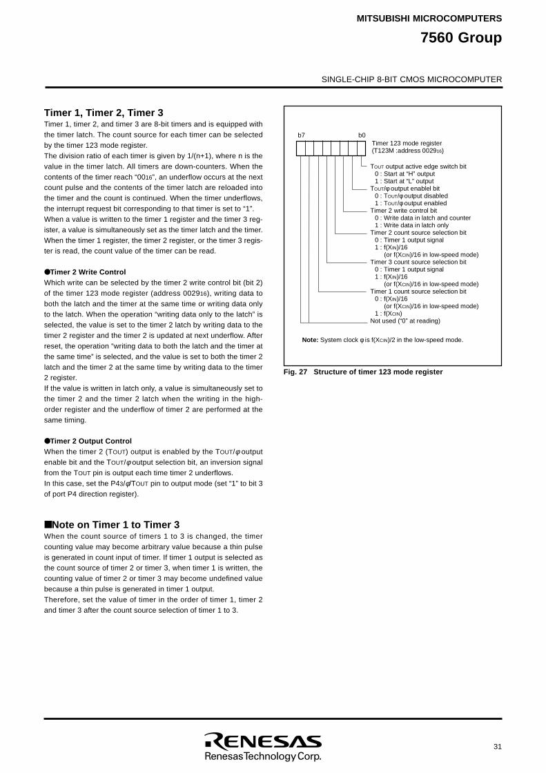
SINGLE-CHIP 8-BIT CMOS MICROCOMPUTER
MITSUBISHI MICROCOMPUTERS
7560 Group
31
Timer 1, Timer 2, Timer 3Timer 1, timer 2, and timer 3 are 8-bit timers and is equipped withthe timer latch. The count source for each timer can be selectedby the timer 123 mode register.The division ratio of each timer is given by 1/(n+1), where n is thevalue in the timer latch. All timers are down-counters. When thecontents of the timer reach “0016”, an underflow occurs at the nextcount pulse and the contents of the timer latch are reloaded intothe timer and the count is continued. When the timer underflows,the interrupt request bit corresponding to that timer is set to “1”.When a value is written to the timer 1 register and the timer 3 reg-ister, a value is simultaneously set as the timer latch and the timer.When the timer 1 register, the timer 2 register, or the timer 3 regis-ter is read, the count value of the timer can be read.
Timer 2 Write ControlWhich write can be selected by the timer 2 write control bit (bit 2)of the timer 123 mode register (address 002916), writing data toboth the latch and the timer at the same time or writing data onlyto the latch. When the operation “writing data only to the latch” isselected, the value is set to the timer 2 latch by writing data to thetimer 2 register and the timer 2 is updated at next underflow. Afterreset, the operation “writing data to both the latch and the timer atthe same time” is selected, and the value is set to both the timer 2latch and the timer 2 at the same time by writing data to the timer2 register.If the value is written in latch only, a value is simultaneously set tothe timer 2 and the timer 2 latch when the writing in the high-order register and the underflow of timer 2 are performed at thesame timing.
Timer 2 Output ControlWhen the timer 2 (TOUT) output is enabled by the TOUT/φ outputenable bit and the TOUT/φ output selection bit, an inversion signalfrom the TOUT pin is output each time timer 2 underflows.In this case, set the P43/φ/TOUT pin to output mode (set “1” to bit 3of port P4 direction register).
Note on Timer 1 to Timer 3When the count source of timers 1 to 3 is changed, the timercounting value may become arbitrary value because a thin pulseis generated in count input of timer. If timer 1 output is selected asthe count source of timer 2 or timer 3, when timer 1 is written, thecounting value of timer 2 or timer 3 may become undefined valuebecause a thin pulse is generated in timer 1 output.Therefore, set the value of timer in the order of timer 1, timer 2and timer 3 after the count source selection of timer 1 to 3.
Fig. 27 Structure of timer 123 mode register
TO
U
T
o
u
t
p
u
t
a
c
t
i
v
e
e
d
g
e
s
w
i
t
c
h
b
i
t0
:
S
t
a
r
t
a
t
“
H
”
o
u
t
p
u
t1
:
S
t
a
r
t
a
t
“
L
”
o
u
t
p
u
tTO
U
T/φ
o
u
t
p
u
t
e
n
a
b
l
e
l
b
i
t0
:
TO
U
T/φ
o
u
t
p
u
t
d
i
s
a
b
l
e
d1
:
TO
U
T/φ
o
u
t
p
u
t
e
n
a
b
l
e
dT
i
m
e
r
2
w
r
i
t
e
c
o
n
t
r
o
l
b
i
t0
:
W
r
i
t
e
d
a
t
a
i
n
l
a
t
c
h
a
n
d
c
o
u
n
t
e
r1
:
W
r
i
t
e
d
a
t
a
i
n
l
a
t
c
h
o
n
l
yT
i
m
e
r
2
c
o
u
n
t
s
o
u
r
c
e
s
e
l
e
c
t
i
o
n
b
i
t0
:
T
i
m
e
r
1
o
u
t
p
u
t
s
i
g
n
a
l1
:
f
(
XI
N)
/
1
6(
o
r
f
(
XC
I
N)
/
1
6
i
n
l
o
w
-
s
p
e
e
d
m
o
d
e
)T
i
m
e
r
3
c
o
u
n
t
s
o
u
r
c
e
s
e
l
e
c
t
i
o
n
b
i
t0
:
T
i
m
e
r
1
o
u
t
p
u
t
s
i
g
n
a
l1
:
f
(
XI
N)
/
1
6(
o
r
f
(
XC
I
N)
/
1
6
i
n
l
o
w
-
s
p
e
e
d
m
o
d
e
)T
i
m
e
r
1
c
o
u
n
t
s
o
u
r
c
e
s
e
l
e
c
t
i
o
n
b
i
t0
:
f
(
XI
N)
/
1
6(
o
r
f
(
XC
I
N)
/
1
6
i
n
l
o
w
-
s
p
e
e
d
m
o
d
e
)1
:
f
(
XC
I
N)N
o
t
u
s
e
d
(
“
0
”
a
t
r
e
a
d
i
n
g
)
Timer 123 mode register(T123M :address 002916)
Note: System clock φ is f(XCIN)/2 in the low-speed mode.
b
7 b0
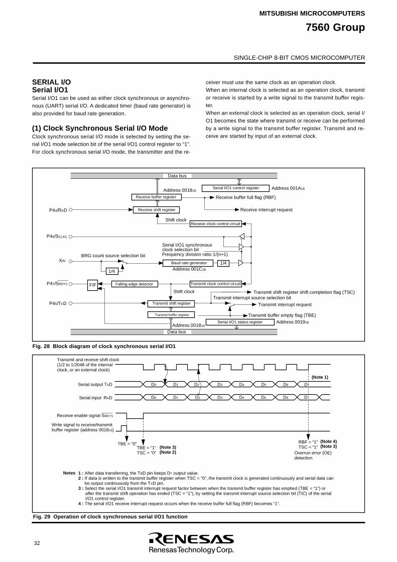
SINGLE-CHIP 8-BIT CMOS MICROCOMPUTER
MITSUBISHI MICROCOMPUTERS
7560 Group
32
SERIAL I/OSerial I/O1Serial I/O1 can be used as either clock synchronous or asynchro-nous (UART) serial I/O. A dedicated timer (baud rate generator) isalso provided for baud rate generation.
(1) Clock Synchronous Serial I/O ModeClock synchronous serial I/O mode is selected by setting the se-rial I/O1 mode selection bit of the serial I/O1 control register to “1”.For clock synchronous serial I/O mode, the transmitter and the re-
ceiver must use the same clock as an operation clock.When an internal clock is selected as an operation clock, transmitor receive is started by a write signal to the transmit buffer regis-ter.When an external clock is selected as an operation clock, serial I/O1 becomes the state where transmit or receive can be performedby a write signal to the transmit buffer register. Transmit and re-ceive are started by input of an external clock.
Fig. 28 Block diagram of clock synchronous serial I/O1
Fig. 29 Operation of clock synchronous serial I/O1 function
P
46/
SC
L
K
1
P
47/
SR
D
Y
1
P
44/
RXD
P45/TXD
XI
N 1
/
4
1/4
F
/
F
Serial I/O1 status register
Serial I/O1 control register
R
e
c
e
i
v
e
b
u
f
f
e
r
r
e
g
i
s
t
e
r
A
d
d
r
e
s
s
0
0
1
81
6
Receive shift register
Receive buffer full flag (RBF)
R
e
c
e
i
v
e
i
n
t
e
r
r
u
p
t
r
e
q
u
e
s
t
Receive clock control circuitS
h
i
f
t
c
l
o
c
k
Serial I/O1 synchronousclock selection bit Frequency division ratio 1/(n+1)
Baud rate generator
A
d
d
r
e
s
s
0
0
1
C1
6
BRG count source selection bit
F
a
l
l
i
n
g
-
e
d
g
e
d
e
t
e
c
t
o
r
Data busAddress 001816
S
h
i
f
t
c
l
o
c
k Transmit shift register shift completion flag (TSC)
Transmit buffer empty flag (TBE)
T
r
a
n
s
m
i
t
i
n
t
e
r
r
u
p
t
r
e
q
u
e
s
t
Transmit interrupt source selection bit
Address 001916
Data bus
A
d
d
r
e
s
s
0
0
1
A1
6
T
r
a
n
s
m
i
t
b
u
f
f
e
r
r
e
g
i
s
t
e
r
T
r
a
n
s
m
i
t
s
h
i
f
t
r
e
g
i
s
t
e
r
T
r
a
n
s
m
i
t
cl
o
c
k
c
o
n
t
r
o
l
c
i
r
c
u
i
t
Receive enable signal SRDY1
D7D0 D1 D2 D3 D4 D5 D6
RBF = “1”TSC = “1”
TBE = “0”TBE = “1”TSC = “0”
T
r
a
n
s
m
i
t
a
n
d
r
e
c
e
i
v
e
s
h
i
f
t
c
l
o
c
k(
1
/
2
t
o
1
/
2
0
4
8
o
f
t
h
e
i
n
t
e
r
n
a
l
c
l
o
c
k
,
o
r
a
n
e
x
t
e
r
n
a
l
c
l
o
c
k
)
S
e
r
i
a
l
o
u
t
p
u
t
TXD
S
e
r
i
a
l
i
n
p
u
t
RXD
W
r
i
t
e
s
i
g
n
a
l
t
o
r
e
c
e
i
v
e
/
t
r
a
n
s
m
i
t
b
u
f
f
e
r
r
e
g
i
s
t
e
r
(
a
d
d
r
e
s
s
0
0
1
81
6)
O
v
e
r
r
u
n
e
r
r
o
r
(
O
E
)
d
e
t
e
c
t
i
o
n
N
o
t
e
s 1
:
A
f
t
e
r
d
a
t
a
t
r
a
n
s
f
e
r
r
i
n
g
,
t
h
e
T
x
D
p
i
n
k
e
e
p
s
D7
o
u
t
p
u
t
v
a
l
u
e
.2
:
I
f
d
a
t
a
i
s
w
r
i
t
t
e
n
t
o
t
h
e
t
r
a
n
s
m
i
t
b
u
f
f
e
r
r
e
g
i
s
t
e
r
w
h
e
n
T
S
C
=
“
0
”
,
t
h
e
t
r
a
n
s
m
i
t
c
l
o
c
k
i
s
g
e
n
e
r
a
t
e
d
c
o
n
t
i
n
u
o
u
s
l
y
a
n
d
s
e
r
i
a
l
d
a
t
a
c
a
n
b
e
o
u
t
p
u
t
c
o
n
t
i
n
u
o
u
s
l
y
f
r
o
m
t
h
e
TXD
p
i
n
.
3
:
S
e
l
e
c
t
t
h
e
s
e
r
i
a
l
I
/
O
1
t
r
a
n
s
m
i
t
i
n
t
e
r
r
u
p
t
r
e
q
u
e
s
t
f
a
c
t
o
r
b
e
t
w
e
e
n
w
h
e
n
t
h
e
t
r
a
n
s
m
i
t
b
u
f
f
e
r
r
e
g
i
s
t
e
r
h
a
s
e
m
p
t
i
e
d
(
T
B
E
=
“
1
”
)
o
r
a
f
t
e
r
t
h
e
t
r
a
n
s
m
i
t
s
h
i
f
t
o
p
e
r
a
t
i
o
n
h
a
s
e
n
d
e
d
(
T
S
C
=
“
1
”
)
,
b
y
s
e
t
t
i
n
g
t
h
e
t
r
a
n
s
m
i
t
i
n
t
e
r
r
u
p
t
s
o
u
r
c
e
s
e
l
e
c
t
i
o
n
b
i
t
(
T
I
C
)
o
f
t
h
e
s
e
r
i
a
l
I
/
O
1
c
o
n
t
r
o
l
r
e
g
i
s
t
e
r
.4
:
T
h
e
s
e
r
i
a
l
I
/
O
1
r
e
c
e
i
v
e
i
n
t
e
r
r
u
p
t
r
e
q
u
e
s
t
o
c
c
u
r
s
w
h
e
n
t
h
e
r
e
c
e
i
v
e
b
u
f
f
e
r
f
u
l
l
f
l
a
g
(
R
B
F
)
b
e
c
o
m
e
s
“
1
”
.
D7D0 D1 D2 D3 D4 D5 D6
( N
o
t
e
1
)
(Note 3)(Note 2)
(Note 3)(Note 4)
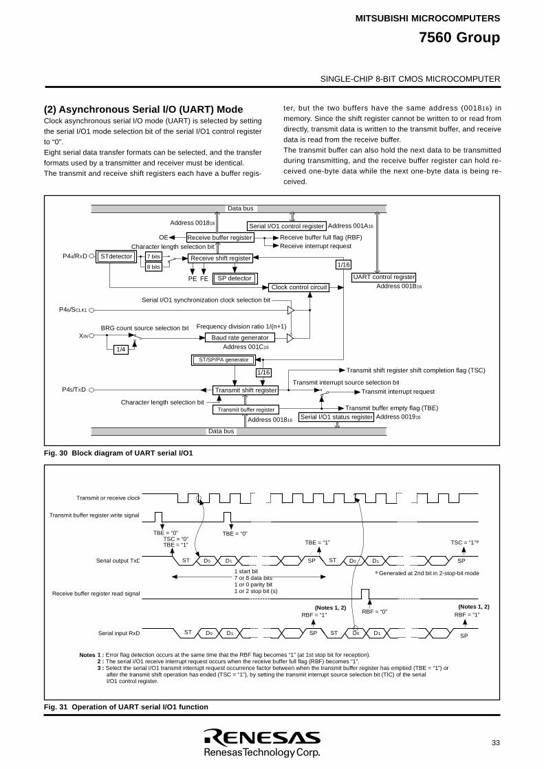
SINGLE-CHIP 8-BIT CMOS MICROCOMPUTER
MITSUBISHI MICROCOMPUTERS
7560 Group
33
(2) Asynchronous Serial I/O (UART) ModeClock asynchronous serial I/O mode (UART) is selected by settingthe serial I/O1 mode selection bit of the serial I/O1 control registerto “0”.Eight serial data transfer formats can be selected, and the transferformats used by a transmitter and receiver must be identical.The transmit and receive shift registers each have a buffer regis-
ter, but the two buffers have the same address (001816) inmemory. Since the shift register cannot be written to or read fromdirectly, transmit data is written to the transmit buffer, and receivedata is read from the receive buffer.The transmit buffer can also hold the next data to be transmittedduring transmitting, and the receive buffer register can hold re-ceived one-byte data while the next one-byte data is being re-ceived.
Fig. 30 Block diagram of UART serial I/O1
Fig. 31 Operation of UART serial I/O1 function
XIN
1/4
O
E
P
E F
E
1/16
1
/
1
6
Data bus
R
e
c
e
i
v
e
b
u
f
f
e
r
r
e
g
i
s
t
e
r
A
d
d
r
e
s
s
0
0
1
81
6
Receive shift register
R
e
c
e
i
v
e
b
u
f
f
e
r
f
u
l
l
f
l
a
g
(
R
B
F
)R
e
c
e
i
v
e
i
n
t
e
r
r
u
p
t
r
e
q
u
e
s
t
B
a
u
d
r
a
t
e
g
e
n
e
r
a
t
o
r
F
r
e
q
u
e
n
c
y
d
i
v
i
s
i
o
n
r
a
t
i
o
1
/
(
n
+
1
)
Address 001C16
S
T
/
S
P
/
P
A
g
e
n
e
r
a
t
o
r
Transmit buffer register
D
a
t
a
b
u
s
T
r
a
n
s
m
i
t
s
h
i
f
t
r
e
g
i
s
t
e
r
Address 001816
T
r
a
n
s
m
i
t
s
h
i
f
t
r
e
g
i
s
t
e
r
s
h
i
f
t
c
o
m
p
l
e
t
i
o
n
f
l
a
g
(
T
S
C
)
T
r
a
n
s
m
i
t
b
u
f
f
e
r
e
m
p
t
y
f
l
a
g
(
T
B
E
)
Transmit interrupt request
Address 001916
S
T
d
e
t
e
c
t
o
r
SP detector U
A
R
T
c
o
n
t
r
o
l
r
e
g
i
s
t
e
rAddress 001B16
Character length selection bit
A
d
d
r
e
s
s
0
0
1
A1
6
B
R
G
c
o
u
n
t
s
o
u
r
c
e
s
e
l
e
c
t
i
o
n
b
i
t
Transmit interrupt source selection bit
S
e
r
i
a
l
I
/
O
1
s
y
n
c
h
r
o
n
i
z
a
t
i
o
n
c
l
o
c
k
s
e
l
e
c
t
i
o
n
b
i
t
Clock control circuit
C
h
a
r
a
c
t
e
r
l
e
n
g
t
h
s
e
l
e
c
t
i
o
n
b
i
t
7
b
i
t
s
8
b
i
t
s
S
e
r
i
a
l
I
/
O
1
c
o
n
t
r
o
l
r
e
g
i
s
t
e
r
P46/SCLK1
S
e
r
i
a
l
I
/
O
1
s
t
a
t
u
s
r
e
g
i
s
t
e
r
P44/RXD
P45/TXD
T
S
C
=
“
0
”T
B
E
=
“
1
”
R
B
F
=
“
0
”
T
B
E
=
“
0
” TBE = “0”
R
B
F
=
“
1
” RBF = “1”
S
TD0 D1 S
P D0 D1STS
P
T
B
E
=
“
1
” TSC = “1”
STD0 D1 SP D0 D1S
T S
P
Transmit buffer register write signal
Generated at 2nd bit in 2-stop-bit mode 1 start bit7 or 8 data bits1 or 0 parity bit1 or 2 stop bit (s)
1
:
E
r
r
o
r
f
l
a
g
d
e
t
e
c
t
i
o
n
o
c
c
u
r
s
a
t
t
h
e
s
a
m
e
t
i
m
e
t
h
a
t
t
h
e
R
B
F
f
l
a
g
b
e
c
o
m
e
s
“
1
”
(
a
t
1
s
t
s
t
o
p
b
i
t
f
o
r
r
e
c
e
p
t
i
o
n
)
.2
:
T
h
e
s
e
r
i
a
l
I
/
O
1
r
e
c
e
i
v
e
i
n
t
e
r
r
u
p
t
r
e
q
u
e
s
t
o
c
c
u
r
s
w
h
e
n
t
h
e
r
e
c
e
i
v
e
b
u
f
f
e
r
f
u
l
l
f
l
a
g
(
R
B
F
)
b
e
c
o
m
e
s
“
1
”
.3
:
S
e
l
e
c
t
t
h
e
s
e
r
i
a
l
I
/
O
1
t
r
a
n
s
m
i
t
i
n
t
e
r
r
u
p
t
r
e
q
u
e
s
t
o
c
c
u
r
r
e
n
c
e
f
a
c
t
o
r
b
e
t
w
e
e
n
w
h
e
n
t
h
e
t
r
a
n
s
m
i
t
b
u
f
f
e
r
r
e
g
i
s
t
e
r
h
a
s
e
m
p
t
i
e
d
(
T
B
E
=
“
1
”
)
o
r
a
f
t
e
r
t
h
e
t
r
a
n
s
m
i
t
s
h
i
f
t
o
p
e
r
a
t
i
o
n
h
a
s
e
n
d
e
d
(
T
S
C
=
“
1
”
)
,
b
y
s
e
t
t
i
n
g
t
h
e
t
r
a
n
s
m
i
t
i
n
t
e
r
r
u
p
t
s
o
u
r
c
e
s
e
l
e
c
t
i
o
n
b
i
t
(
T
I
C
)
o
f
t
h
e
s
e
r
i
a
l
I
/
O
1
c
o
n
t
r
o
l
r
e
g
i
s
t
e
r
.
N
o
t
e
s
S
e
r
i
a
l
o
u
t
p
u
t
T
x
D
S
e
r
i
a
l
i
n
p
u
t
R
x
D
Receive buffer register read signal
Transmit or receive clock
(Notes 1, 2) (Notes 1, 2)
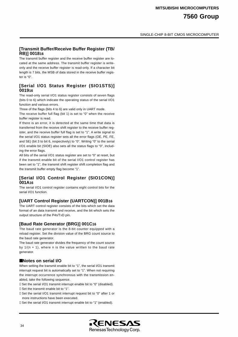
SINGLE-CHIP 8-BIT CMOS MICROCOMPUTER
MITSUBISHI MICROCOMPUTERS
7560 Group
34
[Transmit Buffer/Receive Buffer Register (TB/RB)] 001816The transmit buffer register and the receive buffer register are lo-cated at the same address. The transmit buffer register is write-only and the receive buffer register is read-only. If a character bitlength is 7 bits, the MSB of data stored in the receive buffer regis-ter is “0”.
[Serial I/O1 Status Register (SIO1STS)]001916The read-only serial I/O1 status register consists of seven flags(bits 0 to 6) which indicate the operating status of the serial I/O1function and various errors.Three of the flags (bits 4 to 6) are valid only in UART mode.The receive buffer full flag (bit 1) is set to “0” when the receivebuffer register is read.If there is an error, it is detected at the same time that data istransferred from the receive shift register to the receive buffer reg-ister, and the receive buffer full flag is set to “1”. A write signal tothe serial I/O1 status register sets all the error flags (OE, PE, FE,and SE) (bit 3 to bit 6, respectively) to “0”. Writing “0” to the serialI/O1 enable bit (SIOE) also sets all the status flags to “0”, includ-ing the error flags.All bits of the serial I/O1 status register are set to “0” at reset, butif the transmit enable bit of the serial I/O1 control register hasbeen set to “1”, the transmit shift register shift completion flag andthe transmit buffer empty flag become “1”.
[Serial I/O1 Control Register (SIO1CON)]001A16The serial I/O1 control register contains eight control bits for theserial I/O1 function.
[UART Control Register (UARTCON)] 001B16The UART control register consists of the bits which set the dataformat of an data transmit and receive, and the bit which sets theoutput structure of the P45/TXD pin.
[Baud Rate Generator (BRG)] 001C16The baud rate generator is the 8-bit counter equipped with areload register. Set the division value of the BRG count source tothe baud rate generator.The baud rate generator divides the frequency of the count sourceby 1/(n + 1), where n is the value written to the baud rategenerator.
Notes on serial I/OWhen setting the transmit enable bit to “1”, the serial I/O1 transmitinterrupt request bit is automatically set to “1”. When not requiringthe interrupt occurrence synchronous with the transmission en-abled, take the following sequence.➀ Set the serial I/O1 transmit interrupt enable bit to “0” (disabled).➁ Set the transmit enable bit to “1”.➂ Set the serial I/O1 transmit interrupt request bit to “0” after 1 or
more instructions have been executed.➃ Set the serial I/O1 transmit interrupt enable bit to “1” (enabled).
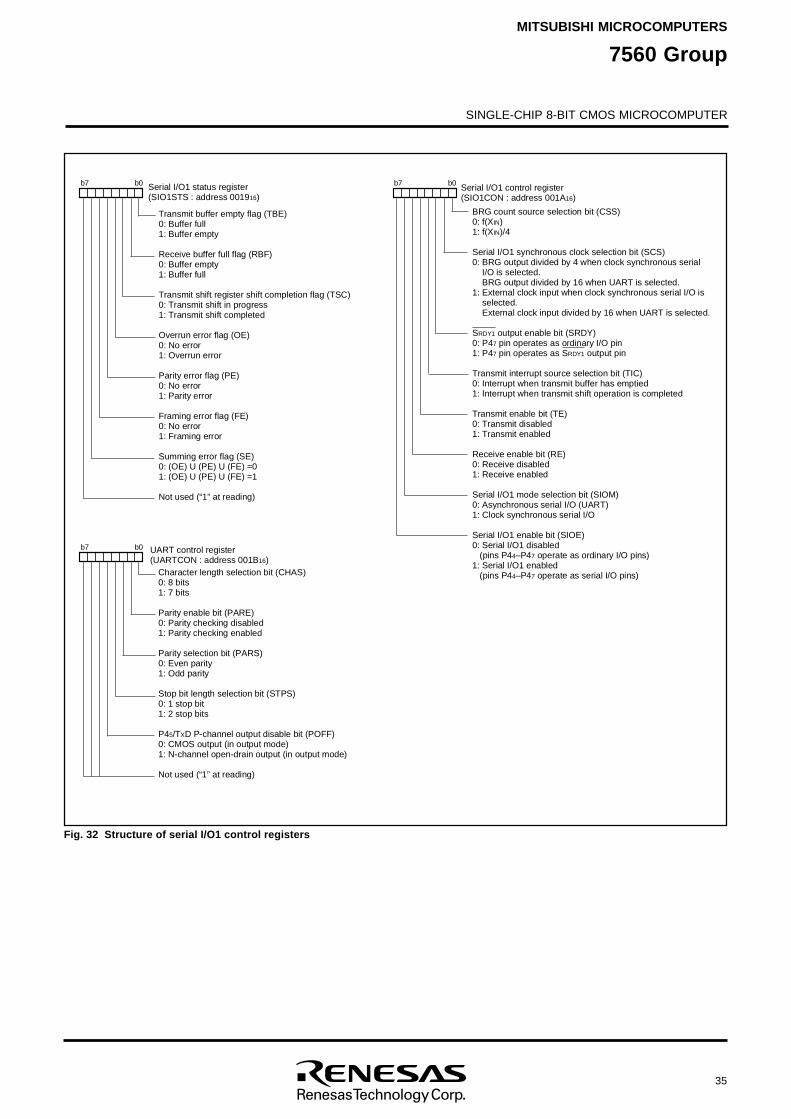
SINGLE-CHIP 8-BIT CMOS MICROCOMPUTER
MITSUBISHI MICROCOMPUTERS
7560 Group
35
Fig. 32 Structure of serial I/O1 control registers
BRG count source selection bit (CSS)0: f(XIN)1: f(XIN)/4
Serial I/O1 synchronous clock selection bit (SCS)0: BRG output divided by 4 when clock synchronous serial I/O is selected. BRG output divided by 16 when UART is selected.
1: External clock input when clock synchronous serial I/O is selected. External clock input divided by 16 when UART is selected.
SRDY1 output enable bit (SRDY)0: P47 pin operates as ordinary I/O pin1: P47 pin operates as SRDY1 output pin
Transmit interrupt source selection bit (TIC)0: Interrupt when transmit buffer has emptied1: Interrupt when transmit shift operation is completed
Transmit enable bit (TE)0: Transmit disabled1: Transmit enabled
Receive enable bit (RE)0: Receive disabled1: Receive enabled
Serial I/O1 mode selection bit (SIOM)0: Asynchronous serial I/O (UART) 1: Clock synchronous serial I/O
Serial I/O1 enable bit (SIOE)0: Serial I/O1 disabled (pins P44–P47 operate as ordinary I/O pins)
1: Serial I/O1 enabled (pins P44–P47 operate as serial I/O pins)
Serial I/O1 control register(SIO1CON : address 001A16)
b7 b0
T
r
a
n
s
m
i
t
b
u
f
f
e
r
e
m
p
t
y
f
l
a
g
(
T
B
E
)0
:
B
u
f
f
e
r
f
u
l
l1
:
B
u
f
f
e
r
e
m
p
t
y
R
e
c
e
i
v
e
b
u
f
f
e
r
f
u
l
l
f
l
a
g
(
R
B
F
)0
:
B
u
f
f
e
r
e
m
p
t
y1
:
B
u
f
f
e
r
f
u
l
l
T
r
a
n
s
m
i
t
s
h
i
f
t
r
e
g
i
s
t
e
r
s
h
i
f
t
c
o
m
p
l
e
t
i
o
n
f
l
a
g
(
T
S
C
)0
:
T
r
a
n
s
m
i
t
s
h
i
f
t
i
n
p
r
o
g
r
e
s
s1
:
T
r
a
n
s
m
i
t
s
h
i
f
t
c
o
m
p
l
e
t
e
d
O
v
e
r
r
u
n
e
r
r
o
r
f
l
a
g
(
O
E
)0
:
N
o
e
r
r
o
r1
:
O
v
e
r
r
u
n
e
r
r
o
r
P
a
r
i
t
y
e
r
r
o
r
f
l
a
g
(
P
E
)0
:
N
o
e
r
r
o
r1
:
P
a
r
i
t
y
e
r
r
o
r
F
r
a
m
i
n
g
e
r
r
o
r
f
l
a
g
(
F
E
)0
:
N
o
e
r
r
o
r1
:
F
r
a
m
i
n
g
e
r
r
o
r
S
u
m
m
i
n
g
e
r
r
o
r
f
l
a
g
(
S
E
)0
:
(
O
E
)
U
(
P
E
)
U
(
F
E
)
=
01
:
(
O
E
)
U
(
P
E
)
U
(
F
E
)
=
1
N
o
t
u
s
e
d
(
“
1
”
a
t
r
e
a
d
i
n
g
)
S
e
r
i
a
l
I
/
O
1
s
t
a
t
u
s
r
e
g
i
s
t
e
r(
S
I
O
1
S
T
S
:
a
d
d
r
e
s
s
0
0
1
91
6)
b7 b0
U
A
R
T
c
o
n
t
r
o
l
r
e
g
i
s
t
e
r
(
U
A
R
T
C
O
N
:
a
d
d
r
e
s
s
0
0
1
B1
6)
Character length selection bit (CHAS)0: 8 bits1: 7 bits
Parity enable bit (PARE)0: Parity checking disabled1: Parity checking enabled
Parity selection bit (PARS)0: Even parity1: Odd parity
Stop bit length selection bit (STPS)0: 1 stop bit1: 2 stop bits
P45/TXD P-channel output disable bit (POFF)0: CMOS output (in output mode)1: N-channel open-drain output (in output mode)
Not used (“1” at reading)
b7 b0
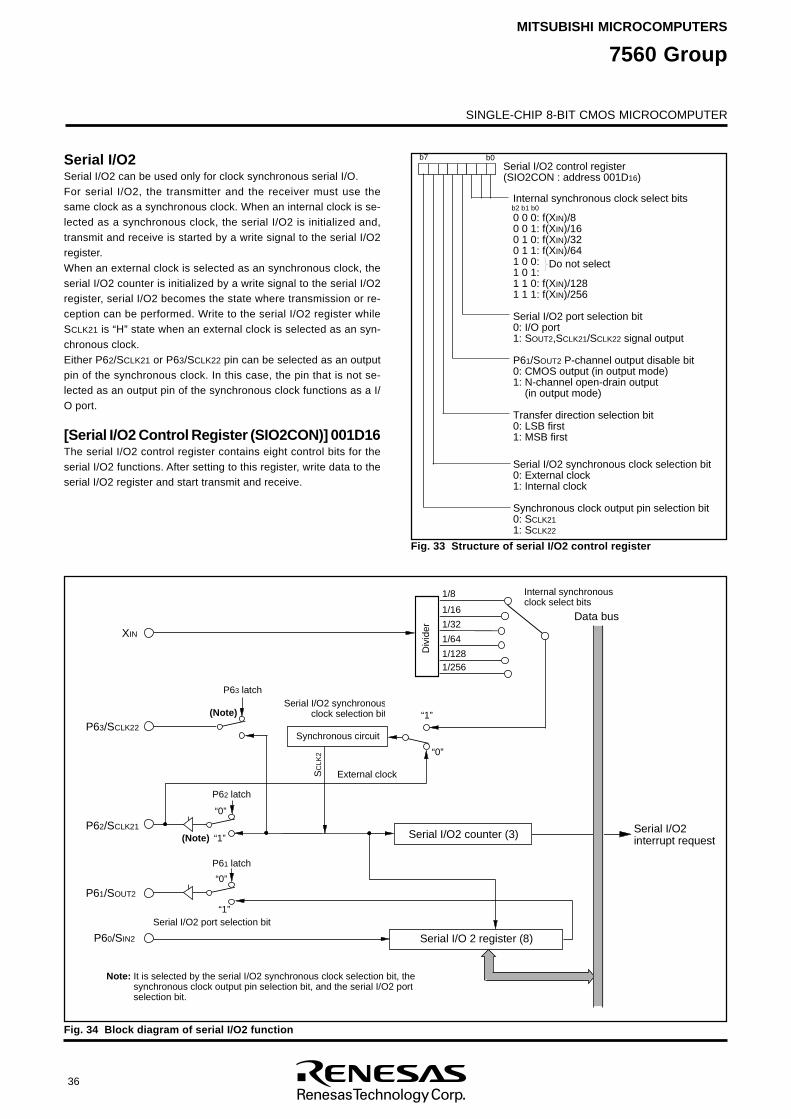
SINGLE-CHIP 8-BIT CMOS MICROCOMPUTER
MITSUBISHI MICROCOMPUTERS
7560 Group
36
Serial I/O2Serial I/O2 can be used only for clock synchronous serial I/O.For serial I/O2, the transmitter and the receiver must use thesame clock as a synchronous clock. When an internal clock is se-lected as a synchronous clock, the serial I/O2 is initialized and,transmit and receive is started by a write signal to the serial I/O2register.When an external clock is selected as an synchronous clock, theserial I/O2 counter is initialized by a write signal to the serial I/O2register, serial I/O2 becomes the state where transmission or re-ception can be performed. Write to the serial I/O2 register whileSCLK21 is “H” state when an external clock is selected as an syn-chronous clock.Either P62/SCLK21 or P63/SCLK22 pin can be selected as an outputpin of the synchronous clock. In this case, the pin that is not se-lected as an output pin of the synchronous clock functions as a I/O port.
[Serial I/O2 Control Register (SIO2CON)] 001D16The serial I/O2 control register contains eight control bits for theserial I/O2 functions. After setting to this register, write data to theserial I/O2 register and start transmit and receive.
Fig. 33 Structure of serial I/O2 control register
Fig. 34 Block diagram of serial I/O2 function
S
e
r
i
a
l
I
/
O
2
c
o
n
t
r
o
l
r
e
g
i
s
t
e
r
(
S
I
O
2
C
O
N
:
a
d
d
r
e
s
s
0
0
1
D1
6)
b7
Internal synchronous clock select bits
0 0 0: f(XIN)/80 0 1: f(XIN)/160 1 0: f(XIN)/320 1 1: f(XIN)/641 0 0:1 0 1:1 1 0: f(XIN)/128 1 1 1: f(XIN)/256
Serial I/O2 port selection bit0: I/O port1: SOUT2,SCLK21/SCLK22 signal output
P61/SOUT2 P-channel output disable bit 0: CMOS output (in output mode)1: N-channel open-drain output (in output mode)
Transfer direction selection bit0: LSB first1: MSB first
Serial I/O2 synchronous clock selection bit 0: External clock1: Internal clock
Synchronous clock output pin selection bit 0: SCLK211: SCLK22
b 0
b2 b1 b0
D
o
n
o
t
s
e
l
e
c
t
XI
N
“ 1
”
“ 0
”
“ 0
”
“ 1
”
“ 0
”
“ 1
”
SC
L
K
2
( N
o
t
e
)
1
/
8
1
/
1
6
1
/
3
2
1
/
6
4
1
/
1
2
81
/
2
5
6
D
a
t
a
b
u
s
S
e
r
i
a
l
I
/
O
2i
n
t
e
r
r
u
p
t
r
e
q
u
e
s
t
S
e
r
i
a
l
I
/
O
2
p
o
r
t
s
e
l
e
c
t
i
o
n
b
i
t
S
e
r
i
a
l
I
/
O
2
c
o
u
n
t
e
r
(
3
)
S
e
r
i
a
l
I
/
O
2
r
e
g
i
s
t
e
r
(
8
)
S
y
n
c
h
r
o
n
o
u
s
c
i
r
c
u
i
t
S
e
r
i
a
l
I
/
O
2
s
y
n
c
h
r
o
n
o
u
sc
l
o
c
k
s
e
l
e
c
t
i
o
n
b
i
t
E
x
t
e
r
n
a
l
c
l
o
c
k
I n
t
e
r
n
a
l
s
y
n
c
h
r
o
n
o
u
s
c
l
o
c
k
s
e
l
e
c
t
b
i
t
s
D i
v
i
d
e
r
P
63
l
a
t
c
h
P
63/
SC
L
K
2
2
P
62/
SC
L
K
2
1
P
61/
SO
U
T
2
P
60/
SI
N
2
P
62
l
a
t
c
h
P
61
l
a
t
c
h
( N
o
t
e
)
N
o
t
e
:
I
t
i
s
s
e
l
e
c
t
e
d
b
y
t
h
e
s
e
r
i
a
l
I
/
O
2
s
y
n
c
h
r
o
n
o
u
s
c
l
o
c
k
s
e
l
e
c
t
i
o
n
b
i
t
,
t
h
e
s
y
n
c
h
r
o
n
o
u
s
c
l
o
c
k
o
u
t
p
u
t
p
i
n
s
e
l
e
c
t
i
o
n
b
i
t
,
a
n
d
t
h
e
s
e
r
i
a
l
I
/
O
2
p
o
r
t
s
e
l
e
c
t
i
o
n
b
i
t
.
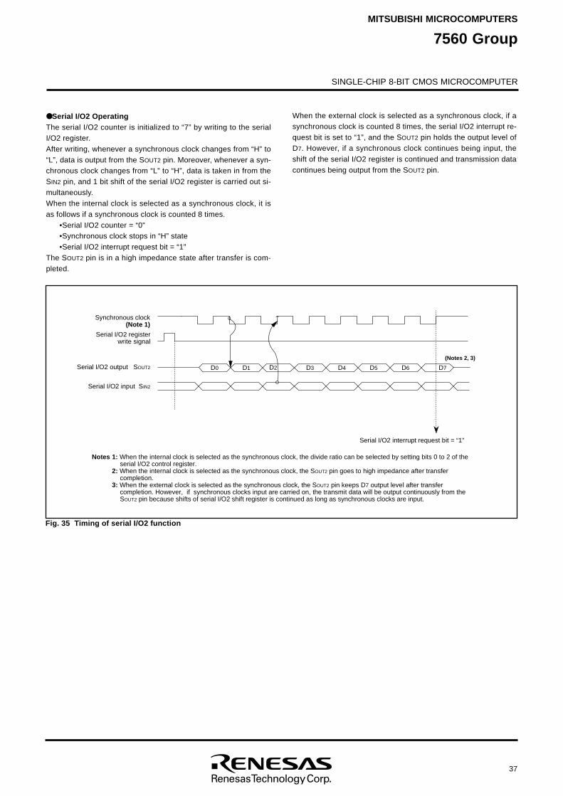
SINGLE-CHIP 8-BIT CMOS MICROCOMPUTER
MITSUBISHI MICROCOMPUTERS
7560 Group
37
Fig. 35 Timing of serial I/O2 function
D7D0 D1 D2 D3 D4 D5 D6
S
y
n
c
h
r
o
n
o
u
s
c
l
o
c
k(
N
o
t
e
1
)
S
e
r
i
a
l
I
/
O
2
o
u
t
p
u
t
SO
U
T
2
S
e
r
i
a
l
I
/
O
2
i
n
p
u
t
SI
N
2
Serial I/O2 registerwrite signal
( N
o
t
e
s
2
,
3
)
S
e
r
i
a
l
I
/
O
2
i
n
t
e
r
r
u
p
t
r
e
q
u
e
s
t
b
i
t
=
“
1
”
1 :
W
h
e
n
t
h
e
i
n
t
e
r
n
a
l
c
l
o
c
k
i
s
s
e
l
e
c
t
e
d
a
s
t
h
e
s
y
n
c
h
r
o
n
o
u
s
c
l
o
c
k
,
t
h
e
d
i
v
i
d
e
r
a
t
i
o
c
a
n
b
e
s
e
l
e
c
t
e
d
b
y
s
e
t
t
i
n
g
b
i
t
s
0
t
o
2
o
f
t
h
e
s
e
r
i
a
l
I
/
O
2
c
o
n
t
r
o
l
r
e
g
i
s
t
e
r
.2
:
W
h
e
n
t
h
e
i
n
t
e
r
n
a
l
c
l
o
c
k
i
s
s
e
l
e
c
t
e
d
a
s
t
h
e
s
y
n
c
h
r
o
n
o
u
s
c
l
o
c
k
,
t
h
e
SO
U
T
2
p
i
n
g
o
e
s
t
o
h
i
g
h
i
m
p
e
d
a
n
c
e
a
f
t
e
r
t
r
a
n
s
f
e
r
c
o
m
p
l
e
t
i
o
n
.3
:
W
h
e
n
t
h
e
e
x
t
e
r
n
a
l
c
l
o
c
k
i
s
s
e
l
e
c
t
e
d
a
s
t
h
e
s
y
n
c
h
r
o
n
o
u
s
c
l
o
c
k
,
t
h
e
SO
U
T
2
p
i
n
k
e
e
p
s
D7
o
u
t
p
u
t
l
e
v
e
l
a
f
t
e
r
t
r
a
n
s
f
e
r
c
o
m
p
l
e
t
i
o
n
. H
o
w
e
v
e
r
,
i
f
s
y
n
c
h
r
o
n
o
u
s
c
l
o
c
k
s
i
n
p
u
t
a
r
e
c
a
r
r
i
e
d
o
n
,
t
h
e
t
r
a
n
s
m
i
t
d
a
t
a
w
i
l
l
b
e
o
u
t
p
u
t
c
o
n
t
i
n
u
o
u
s
l
y
f
r
o
m
t
h
e
SO
U
T
2
p
i
n
b
e
c
a
u
s
e
s
h
i
f
t
s
o
f
s
e
r
i
a
l
I
/
O
2
s
h
i
f
t
r
e
g
i
s
t
e
r
i
s
c
o
n
t
i
n
u
e
d
a
s
l
o
n
g
a
s
s
y
n
c
h
r
o
n
o
u
s
c
l
o
c
k
s
a
r
e
i
n
p
u
t
.
N
o
t
e
s
Serial I/O2 OperatingThe serial I/O2 counter is initialized to “7” by writing to the serialI/O2 register.After writing, whenever a synchronous clock changes from “H” to“L”, data is output from the SOUT2 pin. Moreover, whenever a syn-chronous clock changes from “L” to “H”, data is taken in from theSIN2 pin, and 1 bit shift of the serial I/O2 register is carried out si-multaneously.When the internal clock is selected as a synchronous clock, it isas follows if a synchronous clock is counted 8 times.
•Serial I/O2 counter = “0”•Synchronous clock stops in “H” state•Serial I/O2 interrupt request bit = “1”
The SOUT2 pin is in a high impedance state after transfer is com-pleted.
When the external clock is selected as a synchronous clock, if asynchronous clock is counted 8 times, the serial I/O2 interrupt re-quest bit is set to “1”, and the SOUT2 pin holds the output level ofD7. However, if a synchronous clock continues being input, theshift of the serial I/O2 register is continued and transmission datacontinues being output from the SOUT2 pin.
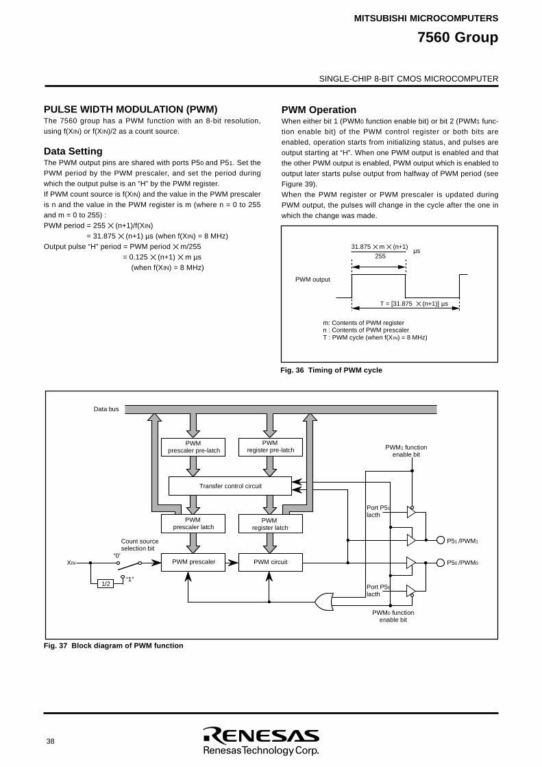
SINGLE-CHIP 8-BIT CMOS MICROCOMPUTER
MITSUBISHI MICROCOMPUTERS
7560 Group
38
PULSE WIDTH MODULATION (PWM)The 7560 group has a PWM function with an 8-bit resolution,using f(XIN) or f(XIN)/2 as a count source.
Data SettingThe PWM output pins are shared with ports P50 and P51. Set thePWM period by the PWM prescaler, and set the period duringwhich the output pulse is an “H” by the PWM register.If PWM count source is f(XIN) and the value in the PWM prescaleris n and the value in the PWM register is m (where n = 0 to 255and m = 0 to 255) :PWM period = 255 (n+1)/f(XIN)
= 31.875 (n+1) µs (when f(XIN) = 8 MHz)Output pulse “H” period = PWM period m/255
= 0.125 (n+1) m µs (when f(XIN) = 8 MHz)
PWM OperationWhen either bit 1 (PWM0 function enable bit) or bit 2 (PWM1 func-tion enable bit) of the PWM control register or both bits areenabled, operation starts from initializing status, and pulses areoutput starting at “H”. When one PWM output is enabled and thatthe other PWM output is enabled, PWM output which is enabled tooutput later starts pulse output from halfway of PWM period (seeFigure 39).When the PWM register or PWM prescaler is updated duringPWM output, the pulses will change in the cycle after the one inwhich the change was made.
Fig. 36 Timing of PWM cycle
Fig. 37 Block diagram of PWM function
31.875 m (n+1)
255µs
T = [31.875 (n+1)] µs
PWM output
m: Contents of PWM registern : Contents of PWM prescalerT : PWM cycle (when f(XIN) = 8 MHz)
D
a
t
a
b
u
s
Count source selection bit
“ 0
”
“ 1
”
P
W
M
p
r
e
s
c
a
l
e
r
p
r
e
-
l
a
t
c
hP
W
M
r
e
g
i
s
t
e
r
p
r
e
-
l
a
t
c
h
PWM prescaler latch
P
W
M
r
e
g
i
s
t
e
r
l
a
t
c
h
Transfer control circuit
PWM circuit
1
/
2
XI
N
P
W
M0
f
u
n
c
t
i
o
ne
n
a
b
l
e
b
i
t
P
51
/
P
W
M1
P
W
M
p
r
e
s
c
a
l
e
r
PWM1 functionenable bit
P
o
r
t
P
51
l
a
c
t
h
P
o
r
t
P
50
l
a
c
t
h
P
50 /
P
W
M0
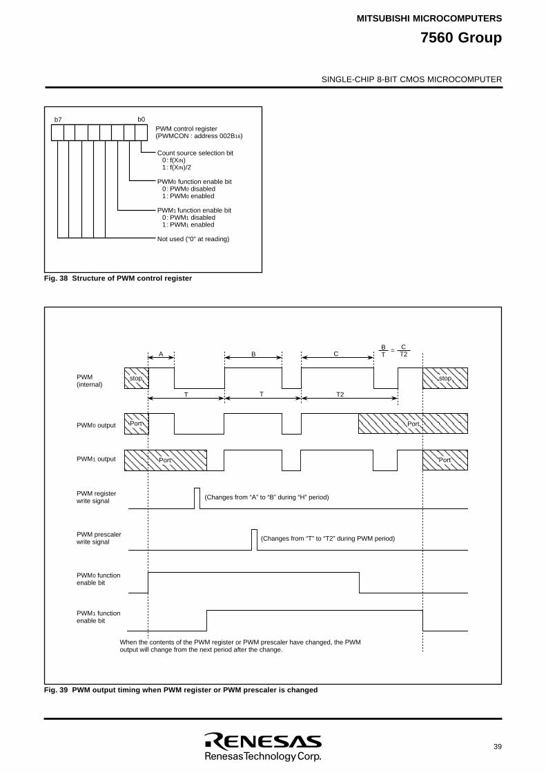
SINGLE-CHIP 8-BIT CMOS MICROCOMPUTER
MITSUBISHI MICROCOMPUTERS
7560 Group
39
Fig. 39 PWM output timing when PWM register or PWM prescaler is changed
Fig. 38 Structure of PWM control register
b
7 b
0P
W
M
c
o
n
t
r
o
l
r
e
g
i
s
t
e
r(
P
W
M
C
O
N
:
a
d
d
r
e
s
s
0
0
2
B1
6)
C
o
u
n
t
s
o
u
r
c
e
s
e
l
e
c
t
i
o
n
b
i
t0 : f
(
XI
N)1: f
(
XI
N)
/
2
P
W
M0
f
u
n
c
t
i
o
n
e
n
a
b
l
e
b
i
t0 : P
W
M0
d
i
s
a
b
l
e
d1: P
W
M0
e
n
a
b
l
e
d
P
W
M1
f
u
n
c
t
i
o
n
e
n
a
b
l
e
b
i
t0 : P
W
M1
d
i
s
a
b
l
e
d1: P
W
M1
e
n
a
b
l
e
d
N
o
t
u
s
e
d
(
“
0
”
a
t
r
e
a
d
i
n
g
)
T T2
CB
T
PWM register write signal
PWM prescaler write signal
(Changes from “A” to “B” during “H” period)
(Changes from “T” to “T2” during PWM period)
PWM(internal)
ABT
CT2
=
stop
PWM0 function enable bit
PWM1 function enable bit
PWM0 output Port
PortPWM1 output
Port
stop
Port
When the contents of the PWM register or PWM prescaler have changed, the PWM output will change from the next period after the change.
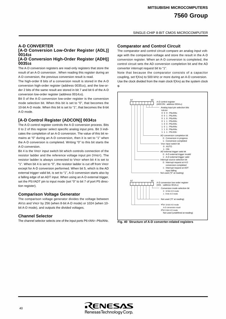
SINGLE-CHIP 8-BIT CMOS MICROCOMPUTER
MITSUBISHI MICROCOMPUTERS
7560 Group
40
A-D CONVERTER[A-D Conversion Low-Order Register (ADL)]001416[A-D Conversion High-Order Register (ADH)]003516The A-D conversion registers are read-only registers that store theresult of an A-D conversion . When reading this register during anA-D conversion, the previous conversion result is read.The high-order 8 bits of a conversion result is stored in the A-Dconversion high-order register (address 003516), and the low-or-der 2 bits of the same result are stored in bit 7 and bit 6 of the A-Dconversion low-order register (address 001416).Bit 0 of the A-D conversion low-order register is the conversionmode selection bit. When this bit is set to “0”, that becomes the10-bit A-D mode. When this bit is set to “1”, that becomes the 8-bitA-D mode.
[A-D Control Register (ADCON)] 003416The A-D control register controls the A-D conversion process. Bits0 to 2 of this register select specific analog input pins. Bit 3 indi-cates the completion of an A-D conversion. The value of this bit re-mains at “0” during an A-D conversion, then it is set to “1” whenthe A-D conversion is completed. Writing “0” to this bit starts theA-D conversion.Bit 4 is the VREF input switch bit which controls connection of theresistor ladder and the reference voltage input pin (VREF). Theresistor ladder is always connected to VREF when bit 4 is set to“1”. When bit 4 is set to “0”, the resistor ladder is cut off from VREF
except for A-D conversion performed. When bit 5, which is the ADexternal trigger valid bit, is set to “1”, A-D conversion starts also bya falling edge of an ADT input. When using an A-D external trigger,set the P57/ADT pin to input mode (set “0” to bit 7 of port P5 direc-tion register).
Comparison Voltage GeneratorThe comparison voltage generator divides the voltage betweenAVSS and VREF by 256 (when 8-bit A-D mode) or 1024 (when 10-bit A-D mode), and outputs the divided voltages.
Channel SelectorThe channel selector selects one of the input ports P67/AN7–P60/AN0.
Comparator and Control CircuitThe comparator and control circuit compare an analog input volt-age with the comparison voltage and store the result in the A-Dconversion register. When an A-D conversion is completed, thecontrol circuit sets the AD conversion completion bit and the ADconverter interrupt request bit to “1”.Note that because the comparator consists of a capacitorcoupling, set f(XIN) to 500 kHz or more during an A-D conversion.Use the clock divided from the main clock f(XIN) as the system clockφ.
Fig. 40 Structure of A-D converter-related registers
A
-
D
c
o
n
t
r
o
l
r
e
g
i
s
t
e
r(
A
D
C
O
N
:
a
d
d
r
e
s
s
0
0
3
41
6)
AD conversion completion bit 0 : Conversion in progress 1 : Conversion completed
Analog input pin selection bitsb2b1b0
0 0 0 : P60/AN0
0 0 1 : P61/AN1
0 1 0 : P62/AN2
0 1 1 : P63/AN3
1 0 0 : P64/AN4
1 0 1 : P65/AN5
1 1 0 : P66/AN6
1 1 1 : P67/AN7
VR
E
F
i
n
p
u
t
s
w
i
t
c
h
b
i
t
0
:
A
U
T
O
1
:
O
NAD external trigger valid bit 0 : A-D external trigger invalid 1 : A-D external trigger valid
b7 b0
Interrupt source selection bit 0 : Interrupt request at A-D conversion completed 1 : Interrupt request at ADT input falling
Not used (“0” at reading)
A
-
D
c
o
n
v
e
r
s
i
o
n
l
o
w
-
o
r
d
e
r
r
e
g
i
s
t
e
r(
A
D
L
:
a
d
d
r
e
s
s
0
0
1
41
6)
Conversion mode selection bit0 : 10-bit A-D mode
1 : 8-bit A-D mode
Not used (“0” at reading)
•For 10-bit A-D mode
A-D conversion result
•For 8-bit A-D mode
Not used (undefined at reading)
b7 b0
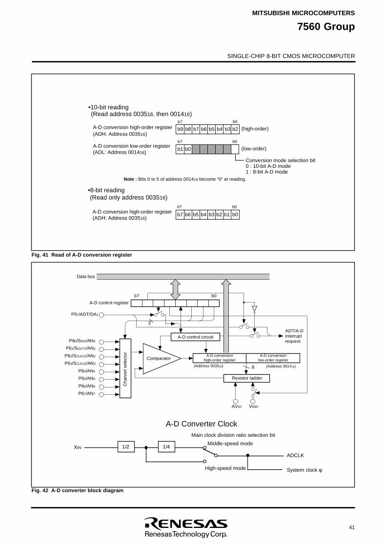
SINGLE-CHIP 8-BIT CMOS MICROCOMPUTER
MITSUBISHI MICROCOMPUTERS
7560 Group
41
Fig. 42 A-D converter block diagram
Fig. 41 Read of A-D conversion register
• 1
0
-
b
i
t
r
e
a
d
i
n
g
(
R
e
a
d
a
d
d
r
e
s
s
0
0
3
51
6
,
t
h
e
n
0
0
1
41
6)
A
-
D
c
o
n
v
e
r
s
i
o
n
h
i
g
h
-
o
r
d
e
r
r
e
g
i
s
t
e
r
(
A
D
H
:
A
d
d
r
e
s
s
0
0
3
51
6)
A
-
D
c
o
n
v
e
r
s
i
o
n
l
o
w
-
o
r
d
e
r
r
e
g
i
s
t
e
r
(
A
D
L
:
A
d
d
r
e
s
s
0
0
1
41
6)b0
b
7 b0
b
1
b7 b6 b
5 b
4 b
3 b2
b
7 b0
b
9 b
8 b7 b6 b
5 b4 b
3 b2
b
7 b
0
(high-order)
( l
o
w
-
o
r
d
e
r
)
N
o
t
e
:
Bi
t
s
0
t
o
5
o
f
a
d
d
r
e
s
s
0
0
1
41
6
b
e
c
o
m
e
“
0
”
a
t
r
e
a
d
i
n
g
.
b1 b0
•8
-
b
i
t
r
e
a
d
i
n
g
(
R
e
a
d
o
n
l
y
a
d
d
r
e
s
s
0
0
3
51
6)
A
-
D
c
o
n
v
e
r
s
i
o
n
h
i
g
h
-
o
r
d
e
r
r
e
g
i
s
t
e
r
(
A
D
H
:
A
d
d
r
e
s
s
0
0
3
51
6)
C
o
n
v
e
r
s
i
o
n
m
o
d
e
s
e
l
e
c
t
i
o
n
b
i
t0
:
1
0
-
b
i
t
A
-
D
m
o
d
e1
:
8
-
b
i
t
A
-
D
m
o
d
e
C
o
m
p
a
r
a
t
o
r
A-D control circuitADT/A-D interrupt request
A
VS
S VR
E
F
P
60/
SI
N
2/
A
N0
Data bus
A
-
D
c
o
n
t
r
o
l
r
e
g
i
s
t
e
r
b
7 b0
A
-
D
c
o
n
v
e
r
s
i
o
nh
i
g
h
-
o
r
d
e
r
r
e
g
i
s
t
e
r
Resistor ladder
C h
a
n
n
e
l
s
e
l
e
c
t
o
r
P67/AN7
P66/AN6
P65/AN5
P64/AN4
P
63/
SC
L
K
2
2/
A
N3
P
62/
SC
L
K2
1/
A
N2
P
61/
SO
U
T2/
A
N1
P
57/
A
D
T
/
D
A2
8
3
( A
d
d
r
e
s
s
0
0
3
51
6)
A
-
D
c
o
n
v
e
r
s
i
o
nl
o
w
-
o
r
d
e
r
r
e
g
i
s
t
e
r
( A
d
d
r
e
s
s
0
0
1
41
6)
1
/
2 1
/
4XI
N
A
D
C
L
K
A
-
D
C
o
n
v
e
r
t
e
r
C
l
o
c
kM
a
i
n
c
l
o
c
k
d
i
v
i
s
i
o
n
r
a
t
i
o
s
e
l
e
c
t
i
o
n
b
i
t
M
i
d
d
l
e
-
s
p
e
e
d
m
o
d
e
H
i
g
h-
s
p
e
e
d
m
o
d
e S
y
s
t
e
m
c
l
o
c
k
φ
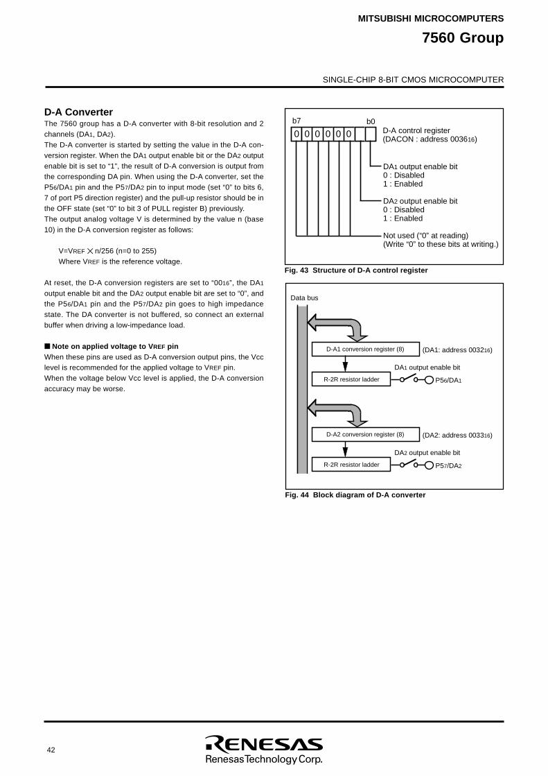
SINGLE-CHIP 8-BIT CMOS MICROCOMPUTER
MITSUBISHI MICROCOMPUTERS
7560 Group
42
D-A ConverterThe 7560 group has a D-A converter with 8-bit resolution and 2channels (DA1, DA2).The D-A converter is started by setting the value in the D-A con-version register. When the DA1 output enable bit or the DA2 outputenable bit is set to “1”, the result of D-A conversion is output fromthe corresponding DA pin. When using the D-A converter, set theP56/DA1 pin and the P57/DA2 pin to input mode (set “0” to bits 6,7 of port P5 direction register) and the pull-up resistor should be inthe OFF state (set “0” to bit 3 of PULL register B) previously.The output analog voltage V is determined by the value n (base10) in the D-A conversion register as follows:
V=VREF n/256 (n=0 to 255)Where VREF is the reference voltage.
At reset, the D-A conversion registers are set to “0016”, the DA1
output enable bit and the DA2 output enable bit are set to “0”, andthe P56/DA1 pin and the P57/DA2 pin goes to high impedancestate. The DA converter is not buffered, so connect an externalbuffer when driving a low-impedance load.
Note on applied voltage to VREF pinWhen these pins are used as D-A conversion output pins, the Vcclevel is recommended for the applied voltage to VREF pin.When the voltage below Vcc level is applied, the D-A conversionaccuracy may be worse.
Fig. 43 Structure of D-A control register
Fig. 44 Block diagram of D-A converter
D
A1
o
u
t
p
u
t
e
n
a
b
l
e
b
i
t0
:
D
i
s
a
b
l
e
d1
:
E
n
a
b
l
e
d
D
A2
o
u
t
p
u
t
e
n
a
b
l
e
b
i
t0
:
D
i
s
a
b
l
e
d1
:
E
n
a
b
l
e
d
N
o
t
u
s
e
d
(
“
0
”
a
t
r
e
a
d
i
n
g
)(
W
r
i
t
e
“
0
”
t
o
t
h
e
s
e
b
i
t
s
a
t
w
r
i
t
i
n
g
.
)
b 7 b
0
D
-
A
c
o
n
t
r
o
l
r
e
g
i
s
t
e
r(
D
A
C
O
N
:
a
d
d
r
e
s
s
0
0
3
61
6)0 0 0 0 0 0
D
a
t
a
b
u
s
P56/DA1
D-A1 conversion register (8)
R
-
2
R
r
e
s
i
s
t
o
r
l
a
d
d
e
r
DA1 output enable bit
(DA1: address 003216)
P57/DA2
D-A2 conversion register (8)
R
-
2
R
r
e
s
i
s
t
o
r
l
a
d
d
e
r
DA2 output enable bit
(DA2: address 003316)
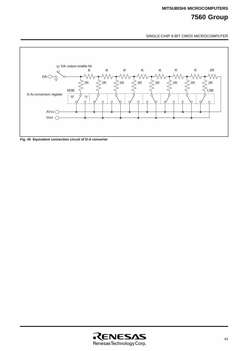
SINGLE-CHIP 8-BIT CMOS MICROCOMPUTER
MITSUBISHI MICROCOMPUTERS
7560 Group
43
Fig. 45 Equivalent connection circuit of D-A converter
A
VS
S
VR
E
F
“ 0
”
“ 1
”
MSB
“0” “ 1
”
R
2
R
R
2R
R
2R
R
2
R
R
2
R
R
2R
R
2
R 2R
LSB
2
R
DAi
D-Ai conversion register
D
Ai
o
u
t
p
u
t
e
n
a
b
l
e
b
i
t
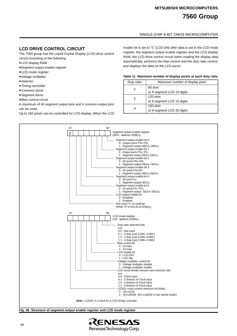
SINGLE-CHIP 8-BIT CMOS MICROCOMPUTER
MITSUBISHI MICROCOMPUTERS
7560 Group
44
LCD DRIVE CONTROL CIRCUITThe 7560 group has the Liquid Crystal Display (LCD) drive controlcircuit consisting of the following.
•LCD display RAM
•Segment output enable register
•LCD mode register
•Voltage multiplier
•Selector
•Timing controller
•Common driver
•Segment driver
•Bias control circuitA maximum of 40 segment output pins and 4 common output pinscan be used.Up to 160 pixels can be controlled for LCD display. When the LCD
Fig. 46 Structure of segment output enable register and LCD mode register
enable bit is set to “1” (LCD ON) after data is set in the LCD moderegister, the segment output enable register and the LCD displayRAM, the LCD drive control circuit starts reading the display dataautomatically, performs the bias control and the duty ratio control,and displays the data on the LCD panel.
Table 11 Maximum number of display pixels at each duty ratio
Duty ratio Maximum number of display pixel
80 dotsor 8 segment LCD 10 digits120 dotsor 8 segment LCD 15 digits160 dotsor 8 segment LCD 20 digits
2
3
4
Segment output enable bit 0 0 : Output ports P30–P35
1 : Segment output SEG18–SEG23
Segment output enable bit 1 0 : Output ports P36, P37
1 : Segment output SEG24,SEG25
Segment output enable bit 2 0 : I/O ports P00–P05
1 : Segment output SEG26–SEG31
Segment output enable bit 3 0 : I/O ports P06,P07
1 : Segment output SEG32,SEG33
Segment output enable bit 4 0 : I/O port P10
1 : Segment output SEG34
Segment output enable bit 5 0 : I/O ports P11–P15
1 : Segment output SEG35–SEG39
LCD output enable bit 0 : Disabled 1 : EnabledNot used (“0” at reading)(Write “0” to this bit at writing.)
Segment output enable register(SEG : address 003816)
b
7 b
0LCD mode register(LM : address 003916)
Duty ratio selection bitsb1b0
0 0 : Not used0 1 : 2 duty (use COM0, COM1)1 0 : 3 duty (use COM0–COM2)1 1 : 4 duty (use COM0–COM3)
Bias control bit 0 : 1/3 bias 1 : 1/2 bias
LCD enable bit 0 : LCD OFF 1 : LCD ON
Voltage multiplier control bit 0 : Voltage multiplier disable 1 : Voltage multiplier enable
LCD circuit divider division ratio selection bitsb6b5
0 0 : Clock input0 1 : 2 division of Clock input1 0 : 4 division of Clock input1 1 : 8 division of Clock input
LCDCK count source selection bit (Note) 0 : f(XCIN)/32 1 : f(XIN)/8192 (f(XCIN)/8192 in low-speed mode)
Note : LCDCK is a clock for a LCD timing controller.
b
7 b0
0
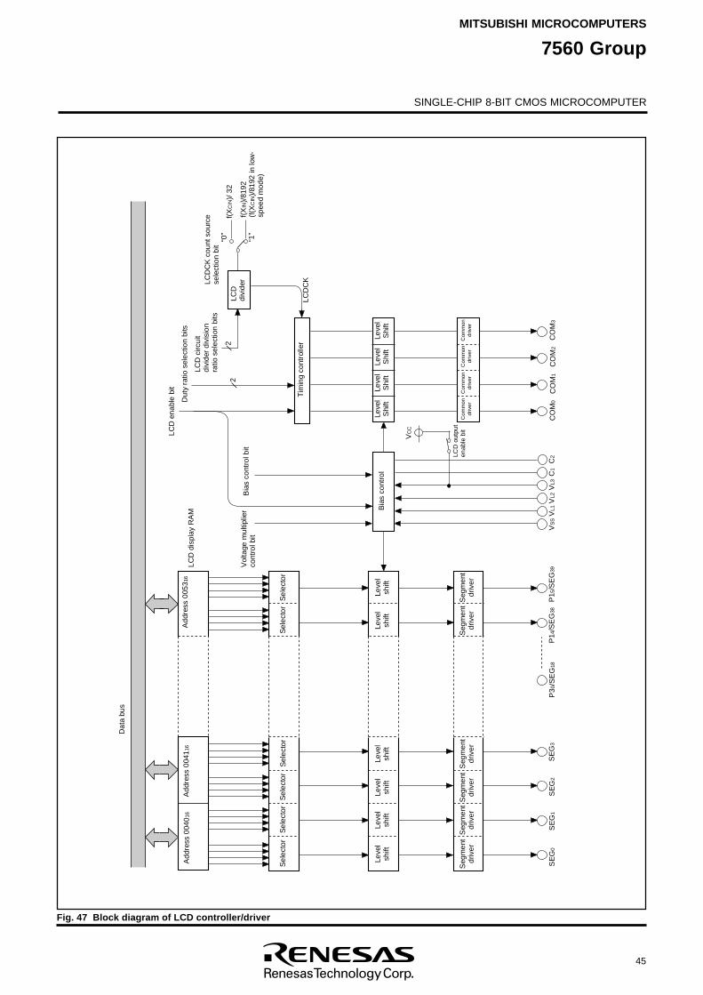
SINGLE-CHIP 8-BIT CMOS MICROCOMPUTER
MITSUBISHI MICROCOMPUTERS
7560 Group
45
Fig. 47 Block diagram of LCD controller/driver
D a
t
a
b
u
s
T
i
m
i
n
g
c
o
n
t
r
o
l
l
e
r
L C D
d i
v
i
d
e
rf (
XI
N)
/
8
1
9
2
( f
(
XC
I
N)
/
8
1
9
2
i
n
l
o
w
-s p
e
e
d
m
o
d
e
)
f ( X
C
I
N)
/
3
2
C O
M
0C
O
M1
C O
M
2C
O
M3
VS
S
VL
1
VL
2
VL
3
S E
G
3S
E
G2
S E
G
1S
E
G0
A
d
d
r
e
s
s
0
0
4
01
6A
d
d
r
e
s
s
0
0
4
11
6
“ 1 ”
“ 0 ”
L C D
C
KL C
D
C
K
c
o
u
n
t
s
o
u
r
c
e
s e
l
e
c
t
i
o
n
b
i
t
L C D
c
i
r
c
u
i
t
d i
v
i
d
e
r
d
i
v
i
s
i
o
n
r a
t
i
o
s
e
l
e
c
t
i
o
n
b
i
t
s
B i
a
s
c
o
n
t
r
o
l
b
i
t
L C D
e
n
a
b
l
e
b
i
t
D u
t
y
r
a
t
i
o
s
e
l
e
c
t
i
o
n
b
i
t
s
22
S e
l
e
c
t
o
r
S e
l
e
c
t
o
r
S e
l
e
c
t
o
r
S
e
l
e
c
t
o
rS
e
l
e
c
t
o
rS
e
l
e
c
t
o
r
L C D
d
i
s
p
l
a
y
R
A
M
A
d
d
r
e
s
s
0
0
5
3 1
6
P 14
/
S
E
G3
8
P 30
/
S
E
G1
8
P 15
/
S
E
G3
9
L
e
v
e
ls
h
i
f
tL
e
v
e
l
s
h
i
f
tL
e
v
e
l
s
h
i
f
tL
e
v
e
l
s
h
i
f
tL
e
v
e
l
s
h
i
f
tL
e
v
e
l
s
h
i
f
t
C
o
m
m
o
nd
r
i
v
e
rC
o
m
m
o
n
d
r
i
v
e
rC
o
m
m
o
n
d
r
i
v
e
rC
o
m
m
o
n
d
r
i
v
e
r
C1
C2
V o
l
t
a
g
e
m
u
l
t
i
p
l
i
e
r
c o
n
t
r
o
l
b
i
t
L
e
v
e
lS
h
i
f
tL
e
v
e
l
S
h
i
f
tL
e
v
e
l
S
h
i
f
tL
e
v
e
l
S
h
i
f
t
S e
g
m
e
n
t
d
r
i
v
e
rS
e
g
m
e
n
td
r
i
v
e
rS
e
g
m
e
n
td
r
i
v
e
rS
e
g
m
e
n
td
r
i
v
e
rS
e
g
m
e
n
td
r
i
v
e
rS
e
g
m
e
n
td
r
i
v
e
r
B i
a
s
c
o
n
t
r
o
l
L C D
o
u
t
p
u
t
e n
a
b
l
e
b
i
t
VC
C
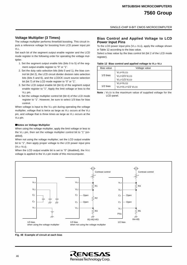
SINGLE-CHIP 8-BIT CMOS MICROCOMPUTER
MITSUBISHI MICROCOMPUTERS
7560 Group
46
Voltage Multiplier (3 Times)The voltage multiplier performs threefold boosting. This circuit in-puts a reference voltage for boosting from LCD power input pinVL1.Set each bit of the segment output enable register and the LCDmode register in the following order for operating the voltage mul-tiplier.
1. Set the segment output enable bits (bits 0 to 5) of the seg-ment output enable register to “0” or “1”.
2. Set the duty ratio selection bits (bits 0 and 1), the bias con-trol bit (bit 2), the LCD circuit divider division ratio selectionbits (bits 5 and 6), and the LCDCK count source selectionbit (bit 7) of the LCD mode register to “0” or “1”.
3. Set the LCD output enable bit (bit 6) of the segment outputenable register to “1”. Apply the limit voltage or less to theVL1 pin.
4. Set the voltage multiplier control bit (bit 4) of the LCD moderegister to “1”. However, be sure to select 1/3 bias for biascontrol.
When voltage is input to the VL1 pin during operating the voltagemultiplier, voltage that is twice as large as VL1 occurs at the VL2
pin, and voltage that is three times as large as VL1 occurs at theVL3 pin.
Notes on Voltage MultiplierWhen using the voltage multiplier, apply the limit voltage or less tothe VL1 pin, then set the voltage multiplier control bit to “1” (en-abled).When not using the voltage multiplier, set the LCD output enablebit to “1”, then apply proper voltage to the LCD power input pins(VL1–VL3).When the LCD output enable bit is set to “0” (disabled), the VCC
voltage is applied to the VL3 pin inside of this microcomputer.
Fig. 48 Example of circuit at each bias
Table 12 Bias control and applied voltage to VL1–VL3
Bias value
1/3 bias
1/2 bias
Voltage value
VL3=VLCD
VL2=2/3 VLCD
VL1=1/3 VLCD
VL3=VLCD
VL2=VL1=1/2 VLCD
Note : VLCD is the maximum value of supplied voltage for theLCD panel.
Bias Control and Applied Voltage to LCDPower Input PinsTo the LCD power input pins (VL1–VL3), apply the voltage shownin Table 12 according to the bias value.Select a bias value by the bias control bit (bit 2 of the LCD moderegister).
VL3
VL
2
C2
C1
VL
1
1
/
3
b
i
a
sw
h
e
n
u
s
i
n
g
t
h
e
v
o
l
t
a
g
e
m
u
l
t
i
p
l
i
e
r
VL3
VL2
C2
C1
VL1
1
/
3
b
i
a
sw
h
e
n
n
o
t
u
s
i
n
g
t
h
e
v
o
l
t
a
g
e
m
u
l
t
i
p
l
i
e
r
O
p
e
n
O
p
e
n
R
2
R
1
R
3
R1=R2=R3
C
o
n
t
r
a
s
t
c
o
n
t
r
o
l
VL
3
VL
2
C2
C1
VL
1
1/2 bias
O
p
e
n
O
p
e
n
R4
R5
R
4
=
R
5
C
o
n
t
r
a
s
t
c
o
n
t
r
o
l
P
X
x
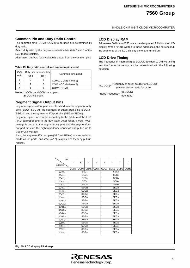
SINGLE-CHIP 8-BIT CMOS MICROCOMPUTER
MITSUBISHI MICROCOMPUTERS
7560 Group
47
(frequency of count source for LCDCK) (divider division ratio for LCD)f(LCDCK)=
f(LCDCK) duty ratioFrame frequency=
Fig. 49 LCD display RAM map
Common Pin and Duty Ratio ControlThe common pins (COM0–COM3) to be used are determined byduty ratio.Select duty ratio by the duty ratio selection bits (bits 0 and 1 of theLCD mode register).After reset, the VCC (VL3) voltage is output from the common pins.
LCD Display RAMAddresses 004016 to 005316 are the designated RAM for the LCDdisplay. When “1” are written to these addresses, the correspond-ing segments of the LCD display panel are turned on.
LCD Drive TimingThe frequency of internal signal LCDCK decided LCD drive timingand the frame frequency can be determined with the followingequation:
Table 13 Duty ratio control and common pins used
Dutyratio
2
34
Common pins used
Notes 1: COM2 and COM3 are open.2: COM3 is open.
Bit 10
11
Bit 01
01
COM0, COM1 (Note 1)COM0–COM2 (Note 2)COM0–COM3
Duty ratio selection bits
Segment Signal Output PinsSegment signal output pins are classified into the segment-onlypins (SEG0–SEG17), the segment or output port pins (SEG18–SEG25), and the segment or I/O port pins (SEG26–SEG39).Segment signals are output according to the bit data of the LCDRAM corresponding to the duty ratio. After reset, a VCC (=VL3)voltage is output to the segment-only pins and the segment/out-put port pins are the high impedance condition and pulled up toVCC (=VL3) voltage.Also, the segment/I/O port pins(SEG26–SEG39) are set to inputmode as I/O ports, and VCC (=VL3) is applied to them by pull-upresistor.
0
0
4
01
6
0
0
4
11
6
0
0
4
21
6
0
0
4
31
6
0
0
4
41
6
0
0
4
51
6
0
0
4
61
6
0
0
4
71
6
0
0
4
81
6
0
0
4
91
6
0
0
4
A1
6
0
0
4
B1
6
0
0
4
C1
6
0
0
4
D1
6
0
0
4
E1
6
0
0
4
F1
6
0
0
5
01
6
0
0
5
11
6
0
0
5
21
6
0
0
5
31
6
B
i
t
A
d
d
r
e
s
s
S
E
G1
S
E
G3
S
E
G5
S
E
G7
S
E
G9
S
E
G1
1
S
E
G1
3
S
E
G1
5
S
E
G1
7
S
E
G1
9
S
E
G2
1
S
E
G2
3
S
E
G2
5
S
E
G2
7
S
E
G2
9
S
E
G3
1
S
E
G3
3
S
E
G3
5
S
E
G3
7
S
E
G3
9
7 6 5 4 3 2 1 0
C
O
M3 C
O
M0C
O
M2 C
O
M1 C
O
M0 COM3 COM2 C
O
M1
SEG0
SEG2
SEG4
SEG6
SEG8
SEG10
SEG12
SEG14
SEG16
SEG18
SEG20
SEG22
SEG24
SEG26
SEG28
SEG30
SEG32
SEG34
SEG36
SEG38
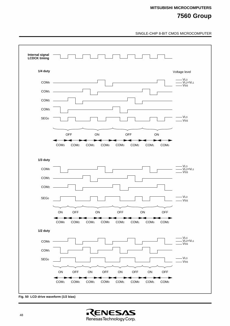
SINGLE-CHIP 8-BIT CMOS MICROCOMPUTER
MITSUBISHI MICROCOMPUTERS
7560 Group
48
Fig. 50 LCD drive waveform (1/2 bias)
I n
t
e
r
n
a
l
s
i
g
n
a
lL
C
D
C
K
t
i
m
i
n
g
1/4 duty V
o
l
t
a
g
e
l
e
v
e
l
VL3VL2=VL1VSS
VL3
VSS
COM0
COM1
COM2
COM3
S
E
G0
O
F
F O
N OFF ON
C
O
M3 C
O
M2 C
O
M1 C
O
M0 COM3 C
O
M2 C
O
M1 C
O
M0
1/3 duty
VL3VL2=VL1VSS
VL3
VSS
O
F
FO
N O
N O
F
F ON O
F
F
1/2 duty
COM0
COM1
COM2
S
E
G0
COM0
COM1
SEG0
VL3VL2=VL1VSS
VL3
VSS
O
F
FO
N O
F
FO
N OFFON O
F
FO
N
C
O
M0 C
O
M2 C
O
M1 C
O
M0 COM2 C
O
M1 C
O
M0 COM2
C
O
M1 C
O
M0 C
O
M1 C
O
M0 COM1 C
O
M0 C
O
M1 COM0
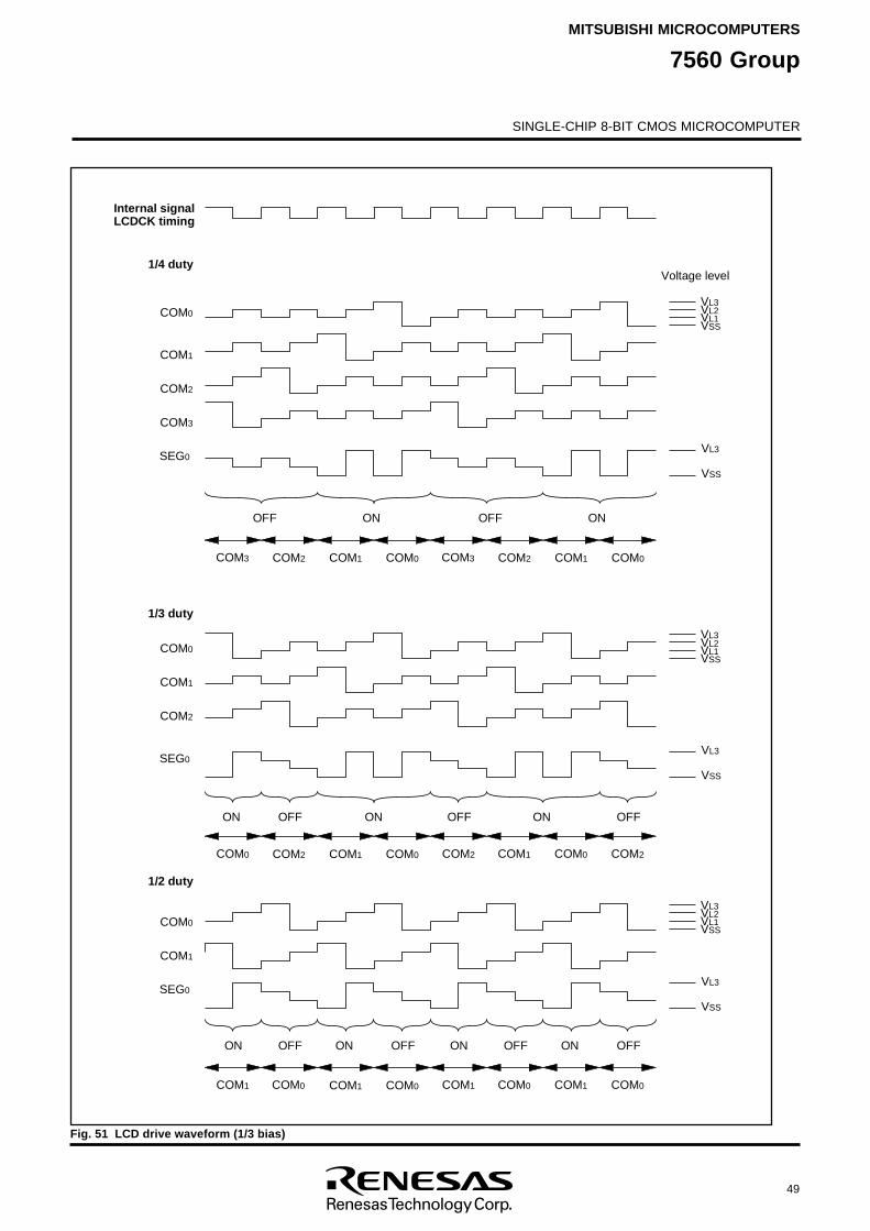
SINGLE-CHIP 8-BIT CMOS MICROCOMPUTER
MITSUBISHI MICROCOMPUTERS
7560 Group
49
Fig. 51 LCD drive waveform (1/3 bias)
I
n
t
e
r
n
a
l
s
i
g
n
a
lL
C
D
C
K
t
i
m
i
n
g
1
/
4
d
u
t
yVoltage level
VL
3
VS
S
C
O
M0
C
O
M1
C
O
M2
C
O
M3
S
E
G0
O
F
F O
N O
F
F O
N
C
O
M3 COM2 C
O
M1 C
O
M0 C
O
M3 C
O
M2 C
O
M1 COM0
1/3 duty
OFFON ON OFF ON OFF
1
/
2
d
u
t
y
C
O
M0
COM1
C
O
M2
S
E
G0
COM0
COM1
SEG0
O
F
FO
N O
F
FO
N OFFON O
F
FON
VL
3VL
2
VS
SVL
1
VL
3VL2
VSSVL1
VL
3
VS
S
VL
3VL
2
VS
SVL
1
VL3
VSS
COM0 COM2 COM1 COM0 COM2 C
O
M1 C
O
M0 COM2
COM1 C
O
M0 C
O
M1 C
O
M0 COM1 C
O
M0 C
O
M1 COM0
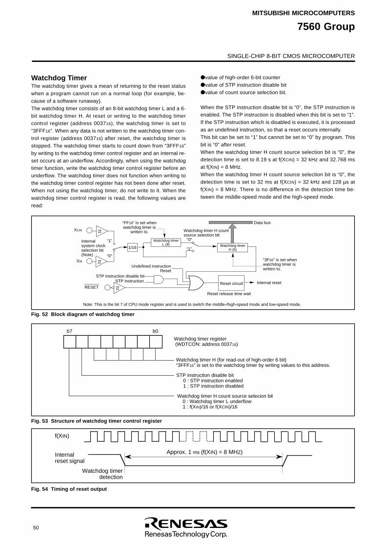
SINGLE-CHIP 8-BIT CMOS MICROCOMPUTER
MITSUBISHI MICROCOMPUTERS
7560 Group
50
Watchdog TimerThe watchdog timer gives a mean of returning to the reset statuswhen a program cannot run on a normal loop (for example, be-cause of a software runaway).The watchdog timer consists of an 8-bit watchdog timer L and a 6-bit watchdog timer H. At reset or writing to the watchdog timercontrol register (address 003716), the watchdog timer is set to“3FFF16”. When any data is not written to the watchdog timer con-trol register (address 003716) after reset, the watchdog timer isstopped. The watchdog timer starts to count down from “3FFF16”by writing to the watchdog timer control register and an internal re-set occurs at an underflow. Accordingly, when using the watchdogtimer function, write the watchdog timer control register before anunderflow. The watchdog timer does not function when writing tothe watchdog timer control register has not been done after reset.When not using the watchdog timer, do not write to it. When thewatchdog timer control register is read, the following values areread:
value of high-order 6-bit counter value of STP instruction disable bit value of count source selection bit.
When the STP instruction disable bit is “0”, the STP instruction isenabled. The STP instruction is disabled when this bit is set to “1”.If the STP instruction which is disabled is executed, it is processedas an undefined instruction, so that a reset occurs internally.This bit can be set to “1” but cannot be set to “0” by program. Thisbit is “0” after reset.When the watchdog timer H count source selection bit is “0”, thedetection time is set to 8.19 s at f(XCIN) = 32 kHz and 32.768 msat f(XIN) = 8 MHz.When the watchdog timer H count source selection bit is “0”, thedetection time is set to 32 ms at f(XCIN) = 32 kHz and 128 µs atf(XIN) = 8 MHz. There is no difference in the detection time be-tween the middle-speed mode and the high-speed mode.
Fig. 52 Block diagram of watchdog timer
Fig. 53 Structure of watchdog timer control register
Fig. 54 Timing of reset output
XIN
Data bus
XCIN
“1”
“0”
Internal system clock selection bit(Note)
“0”
“1”1/16
Watchdog timer H count source selection bit
Reset circuit
Undefined instructionReset
“3F16” is set when watchdog timer is written to.
Internal resetRESET
Reset release time wait
“FF16” is set when watchdog timer is
written to.
STP instructionSTP instruction disable bit
Watchdog timerH (6)
Watchdog timerL (8)
Note: This is the bit 7 of CPU mode register and is used to switch the middle-/high-speed mode and low-speed mode.
b
7 b
0
W
a
t
c
h
d
o
g
t
i
m
e
r
r
e
g
i
s
t
e
r
(
W
D
T
C
O
N
:
a
d
d
r
e
s
s
0
0
3
71
6)
S
T
P
i
n
s
t
r
u
c
t
i
o
n
d
i
s
a
b
l
e
b
i
t
0
:
S
T
P
i
n
s
t
r
u
c
t
i
o
n
e
n
a
b
l
e
d
1
:
S
T
P
i
n
s
t
r
u
c
t
i
o
n
d
i
s
a
b
l
e
d
W
a
t
c
h
d
o
g
t
i
m
e
r
H
c
o
u
n
t
s
o
u
r
c
e
s
e
l
e
c
i
o
n
b
i
t
0
:
W
a
t
c
h
d
o
g
t
i
m
e
r
L
u
n
d
e
r
f
l
o
w
1
:
f
(
XI
N)
/
1
6
o
r
f
(
XC
I
N)
/
1
6
Watchdog timer H (for read-out of high-order 6 bit)“3FFF16” is set to the watchdog timer by writing values to this address.
I n
t
e
r
n
a
l
r
e
s
e
t
s
i
g
n
a
l
W
a
t
c
h
d
o
g
t
i
m
e
rd
e
t
e
c
t
i
o
n
Approx. 1 ms (f(XIN) = 8 MHZ)
f (
XI
N)
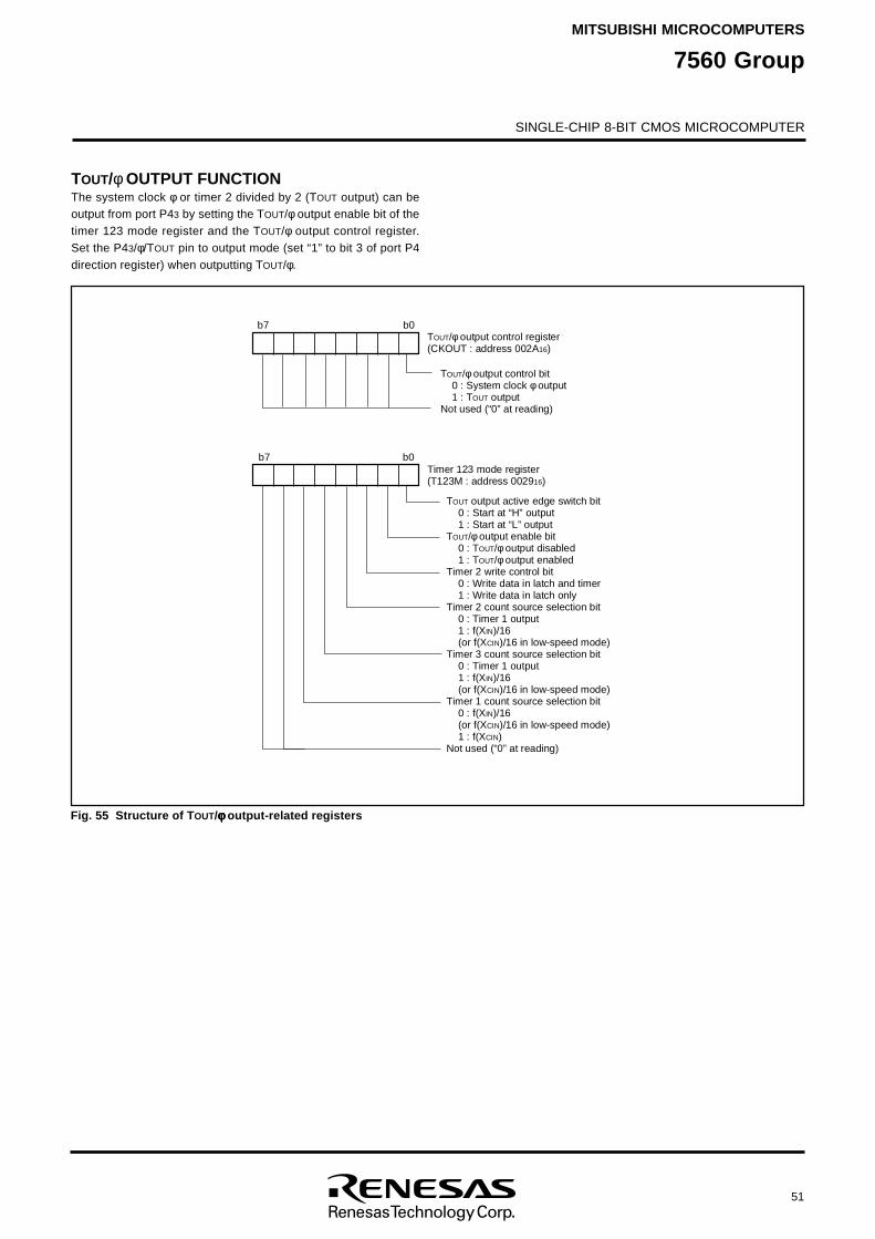
SINGLE-CHIP 8-BIT CMOS MICROCOMPUTER
MITSUBISHI MICROCOMPUTERS
7560 Group
51
TOUT/φ OUTPUT FUNCTIONThe system clock φ or timer 2 divided by 2 (TOUT output) can beoutput from port P43 by setting the TOUT/φ output enable bit of thetimer 123 mode register and the TOUT/φ output control register.Set the P43/φ/TOUT pin to output mode (set “1” to bit 3 of port P4direction register) when outputting TOUT/φ.
Fig. 55 Structure of TOUT/φφφφφ output-related registers
TO
U
T/φ
o
u
t
p
u
t
c
o
n
t
r
o
l
b
i
t
0
:
S
y
s
t
e
m
c
l
o
c
k
φ
o
u
t
p
u
t
1
:
TO
U
T
o
u
t
p
u
tN
o
t
u
s
e
d
(
“
0
”
a
t
r
e
a
d
i
n
g
)
TOUT/φ output control register(CKOUT : address 002A16)
b7 b0Timer 123 mode register(T123M : address 002916)
TOUT output active edge switch bit0 : Start at “H” output1 : Start at “L” output
TOUT/φ output enable bit0 : TOUT/φ output disabled1 : TOUT/φ output enabled
Timer 2 write control bit0 : Write data in latch and timer1 : Write data in latch only
Timer 2 count source selection bit0 : Timer 1 output1 : f(XIN)/16(or f(XCIN)/16 in low-speed mode)
Timer 3 count source selection bit0 : Timer 1 output1 : f(XIN)/16(or f(XCIN)/16 in low-speed mode)
Timer 1 count source selection bit0 : f(XIN)/16(or f(XCIN)/16 in low-speed mode)1 : f(XCIN)
Not used (“0” at reading)
b
7 b
0
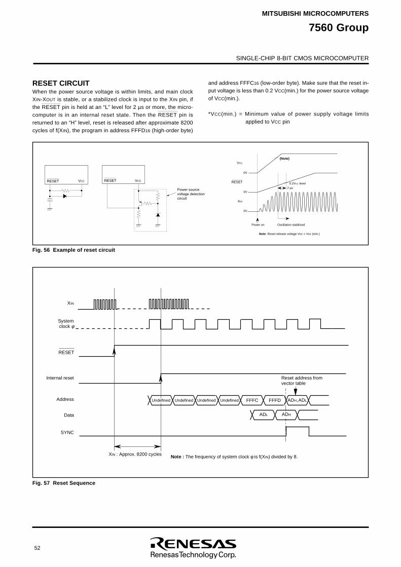
SINGLE-CHIP 8-BIT CMOS MICROCOMPUTER
MITSUBISHI MICROCOMPUTERS
7560 Group
52
Fig. 56 Example of reset circuit
RESET CIRCUITWhen the power source voltage is within limits, and main clockXIN-XOUT is stable, or a stabilized clock is input to the XIN pin, ifthe RESET pin is held at an “L” level for 2 µs or more, the micro-computer is in an internal reset state. Then the RESET pin isreturned to an “H” level, reset is released after approximate 8200cycles of f(XIN), the program in address FFFD16 (high-order byte)
Fig. 57 Reset Sequence
and address FFFC16 (low-order byte). Make sure that the reset in-put voltage is less than 0.2 VCC(min.) for the power source voltageof VCC(min.).
*VCC(min.) = Minimum value of power supply voltage limitsapplied to VCC pin
VC
CR
E
S
E
T VC
CR
E
S
E
T
Power source voltage detection circuit
VC
C
R
E
S
E
T
P
o
w
e
r
o
n
0 .
2
VC
C
l
e
v
e
l
O
s
c
i
l
l
a
t
i
o
n
s
t
a
b
i
l
i
z
e
d
2 µs
XI
N
0
V
0
V
0
V
( N
o
t
e
)
N
o
t
e:
R
e
s
e
t
r
e
l
e
a
s
e
v
o
l
t
a
g
e
V
c
c
=
V
c
c
(
m
i
n
.
)
A
DL
FFFC FFFD A
DH,Undefined
XI
N
:
A
p
p
r
o
x
.
8
2
0
0
c
y
c
l
e
s N
o
t
e
:
T
h
e
f
r
e
q
u
e
n
c
y
o
f
s
y
s
t
e
m
c
l
o
c
k
φ
i
s
f
(
XI
N)
d
i
v
i
d
e
d
b
y
8
.
Reset address from vector table
R
E
S
E
T
I
n
t
e
r
n
a
l
r
e
s
e
t
Address
Data
SYNC
S
y
s
t
e
mc
l
o
c
k
φ
XIN
ADH
ADLUndefined U
n
d
e
f
i
n
e
d U
n
d
e
f
i
n
e
d
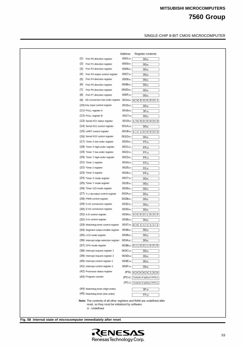
SINGLE-CHIP 8-BIT CMOS MICROCOMPUTER
MITSUBISHI MICROCOMPUTERS
7560 Group
53
Fig. 58 Internal state of microcomputer immediately after reset
N
o
t
e
:
T
h
e
c
o
n
t
e
n
t
s
o
f
a
l
l
o
t
h
e
r
r
e
g
i
s
t
e
r
s
a
n
d
R
A
M
a
r
e
u
n
d
e
f
i
n
e
d
a
f
t
e
r
r
e
s
e
t
,
s
o
t
h
e
y
m
u
s
t
b
e
i
n
i
t
i
a
l
i
z
e
d
b
y
s
o
f
t
w
a
r
e
.
:
U
n
d
e
f
i
n
e
d
Register contentsA
d
d
r
e
s
s
0
0
0
11
6
0
0
0
31
6
000516
0
0
0
71
6
0
0
0
91
6
0
0
0
B1
6
000D16
0
0
0
F1
6
001416
001616
0
0
1
71
6
0
0
1
91
6
001A16
001B16
001D16
002016
0
0
2
11
6
0
0
2
21
6
0
0
2
31
6
002416
002516
0
0
2
61
6
0
0
2
71
6
002816
002916
0
0
2
A1
6
0
0
2
B1
6
0
0
3
21
6
003316
003416
003616
003716
0
0
3
81
6
0
0
3
91
6
003A16
003B16
003C16
003D16
0
0
3
E1
6
003F16
( P
S
)
(PCH)
(PCL)
( 1
0
)
( 1
1
)
( 1
2
)
( 1
3
)
( 1
4
)
( 1
5
)
(16)
( 1
7
)
(18)
( 1
9
)
( 2
0
)
( 2
1
)
(22)
(23)
( 2
4
)
( 2
5
)
(26)
(27)
( 2
8
)
( 2
9
)
( 3
0
)
(31)
(32)
( 3
3
)
( 3
4
)
( 1
)
( 2
)
( 3
)
( 4
)
( 5
)
( 6
)
( 7
)
( 8
)
( 9
)
( 3
5
)
( 3
6
)
( 3
7
)
(38)
(39)
(40)
( 4
1
)
( 4
2
)
( 4
3
)
T
i
m
e
r
Y
l
o
w
-
o
r
d
e
r
r
e
g
i
s
t
e
r
P
o
r
t
P
5
d
i
r
e
c
t
i
o
n
r
e
g
i
s
t
e
r
P
o
r
t
P
6
d
i
r
e
c
t
i
o
n
r
e
g
i
s
t
e
r
P
U
L
L
r
e
g
i
s
t
e
r
B
T
i
m
e
r
Y
h
i
g
h
-
o
r
d
e
r
r
e
g
i
s
t
e
r
S
e
r
i
a
l
I
/
O
1
c
o
n
t
r
o
l
r
e
g
i
s
t
e
r
UART control register
T
i
m
e
r
X
h
i
g
h
-
o
r
d
e
r
r
e
g
i
s
t
e
r
Timer X low-order register
Timer X mode register
T
i
m
e
r
Y
m
o
d
e
r
e
g
i
s
t
e
r
Timer 123 mode register
S
e
r
i
a
l
I
/
O
1
s
t
a
t
u
s
r
e
g
i
s
t
e
r
P
o
r
t
P
7
d
i
r
e
c
t
i
o
n
r
e
g
i
s
t
e
r
A-D control register
S
e
g
m
e
n
t
o
u
t
p
u
t
e
n
a
b
l
e
r
e
g
i
s
t
e
r
L C
D
m
o
d
e
r
e
g
i
s
t
e
r
P
U
L
L
r
e
g
i
s
t
e
r
A
Interrupt edge selection register
C
P
U
m
o
d
e
r
e
g
i
s
t
e
r
Interrupt request register 1
Interrupt request register 2
Interrupt control register 1
I n
t
e
r
r
u
p
t
c
o
n
t
r
o
l
r
e
g
i
s
t
e
r
2
P
r
o
c
e
s
s
o
r
s
t
a
t
u
s
r
e
g
i
s
t
e
r
P
r
o
g
r
a
m
c
o
u
n
t
e
r
P
o
r
t
P
4
d
i
r
e
c
t
i
o
n
r
e
g
i
s
t
e
r
P
o
r
t
P
2
d
i
r
e
c
t
i
o
n
r
e
g
i
s
t
e
r
P
o
r
t
P
3
o
u
t
p
u
t
c
o
n
t
r
o
l
r
e
g
i
s
t
e
r
P
o
r
t
P
1
d
i
r
e
c
t
i
o
n
r
e
g
i
s
t
e
r
P
o
r
t
P
0
d
i
r
e
c
t
i
o
n
r
e
g
i
s
t
e
r
Timer 1 register
Timer 2 register
Timer 3 register
A
D
c
o
n
v
e
r
s
i
o
n
l
o
w
-
o
r
d
e
r
r
e
g
i
s
t
e
r
1 1 1 0 0 0 00
1 0 0 0 0 0 00
0 0 1 1 1 1 11
1 0 0 1 0 000
1
0
01
6
0016
0016
0
01
6
0
01
6
0
01
6
FF16
0
01
6
0
01
6
0
01
6
0
01
6
0
01
6
0
01
6
0
01
6
0
01
6
FF16
FF16
0
01
6
0
01
6
0
01
6
3
F1
6
0
01
6
0
01
6
0
01
6
0
01
6
0
01
6
0016
0
01
6
0
01
6
F
F1
6
F
F1
6
Contents of address FFFD16
Contents of address FFFC16
D-
A
c
o
n
t
r
o
l
r
e
g
i
s
t
e
r
W
a
t
c
h
d
o
g
t
i
m
e
r
c
o
n
t
r
o
l
r
e
g
i
s
t
e
r
D
-
A
1
c
o
n
v
e
r
s
i
o
n
r
e
g
i
s
t
e
r
D-A2 conversion register
S
e
r
i
a
l
I
/
O
2
c
o
n
t
r
o
l
r
e
g
i
s
t
e
r
TO
U
T/φ
o
u
t
p
u
t
c
o
n
t
r
o
l
r
e
g
i
s
t
e
r
P
W
M
c
o
n
t
r
o
l
r
e
g
i
s
t
e
r
Watchdog timer (high-order)(44)
Watchdog timer (low-order)
F
F1
6
0116
0016
0 0 0 1 0 000
3F16
F
F1
6( 4
5
)
001516K
e
y
i
n
p
u
t
c
o
n
t
r
o
l
r
e
g
i
s
t
e
r 0
01
6
0 0 0 0 10
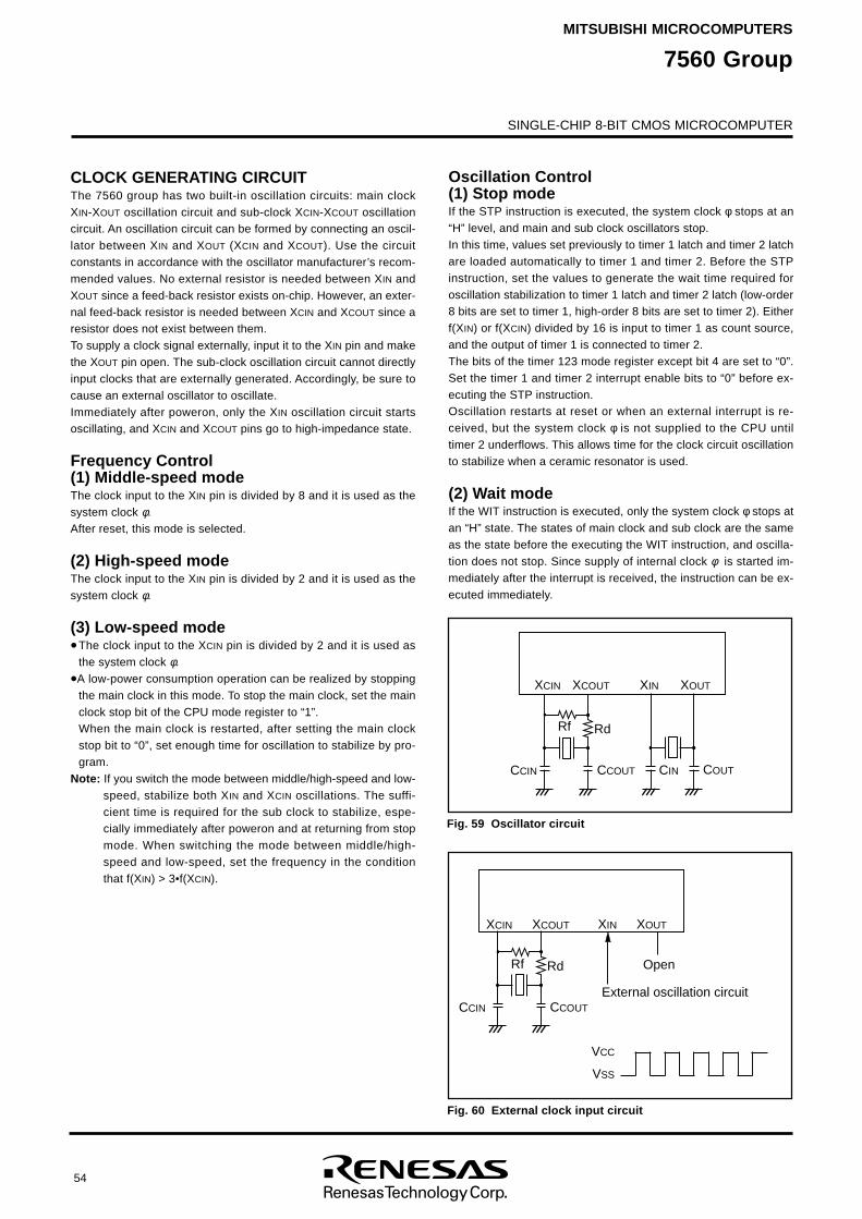
SINGLE-CHIP 8-BIT CMOS MICROCOMPUTER
MITSUBISHI MICROCOMPUTERS
7560 Group
54
Fig. 59 Oscillator circuit
Fig. 60 External clock input circuit
CLOCK GENERATING CIRCUITThe 7560 group has two built-in oscillation circuits: main clockXIN-XOUT oscillation circuit and sub-clock XCIN-XCOUT oscillationcircuit. An oscillation circuit can be formed by connecting an oscil-lator between XIN and XOUT (XCIN and XCOUT). Use the circuitconstants in accordance with the oscillator manufacturer’s recom-mended values. No external resistor is needed between XIN andXOUT since a feed-back resistor exists on-chip. However, an exter-nal feed-back resistor is needed between XCIN and XCOUT since aresistor does not exist between them.To supply a clock signal externally, input it to the XIN pin and makethe XOUT pin open. The sub-clock oscillation circuit cannot directlyinput clocks that are externally generated. Accordingly, be sure tocause an external oscillator to oscillate.Immediately after poweron, only the XIN oscillation circuit startsoscillating, and XCIN and XCOUT pins go to high-impedance state.
Frequency Control(1) Middle-speed modeThe clock input to the XIN pin is divided by 8 and it is used as thesystem clock φ.After reset, this mode is selected.
(2) High-speed modeThe clock input to the XIN pin is divided by 2 and it is used as thesystem clock φ.
(3) Low-speed mode•The clock input to the XCIN pin is divided by 2 and it is used as
the system clock φ.
•A low-power consumption operation can be realized by stoppingthe main clock in this mode. To stop the main clock, set the mainclock stop bit of the CPU mode register to “1”.When the main clock is restarted, after setting the main clockstop bit to “0”, set enough time for oscillation to stabilize by pro-gram.
Note: If you switch the mode between middle/high-speed and low-speed, stabilize both XIN and XCIN oscillations. The suffi-cient time is required for the sub clock to stabilize, espe-cially immediately after poweron and at returning from stopmode. When switching the mode between middle/high-speed and low-speed, set the frequency in the conditionthat f(XIN) > 3•f(XCIN).
Oscillation Control(1) Stop modeIf the STP instruction is executed, the system clock φ stops at an“H” level, and main and sub clock oscillators stop.In this time, values set previously to timer 1 latch and timer 2 latchare loaded automatically to timer 1 and timer 2. Before the STPinstruction, set the values to generate the wait time required foroscillation stabilization to timer 1 latch and timer 2 latch (low-order8 bits are set to timer 1, high-order 8 bits are set to timer 2). Eitherf(XIN) or f(XCIN) divided by 16 is input to timer 1 as count source,and the output of timer 1 is connected to timer 2.The bits of the timer 123 mode register except bit 4 are set to “0”.Set the timer 1 and timer 2 interrupt enable bits to “0” before ex-ecuting the STP instruction.Oscillation restarts at reset or when an external interrupt is re-ceived, but the system clock φ is not supplied to the CPU untiltimer 2 underflows. This allows time for the clock circuit oscillationto stabilize when a ceramic resonator is used.
(2) Wait modeIf the WIT instruction is executed, only the system clock φ stops atan “H” state. The states of main clock and sub clock are the sameas the state before the executing the WIT instruction, and oscilla-tion does not stop. Since supply of internal clock φ is started im-mediately after the interrupt is received, the instruction can be ex-ecuted immediately.
XC
I
N
CI
N CO
U
TCC
I
N CC
O
U
T
R
f R
d
XC
O
U
T XI
N XO
U
T
XI
N
XO
U
T
E
x
t
e
r
n
a
l
o
s
c
i
l
l
a
t
i
o
n
c
i
r
c
u
i
t
O
p
e
n
VCC
VSS
CC
I
N CC
O
U
T
R
f R
d
XC
I
N
XC
O
U
T
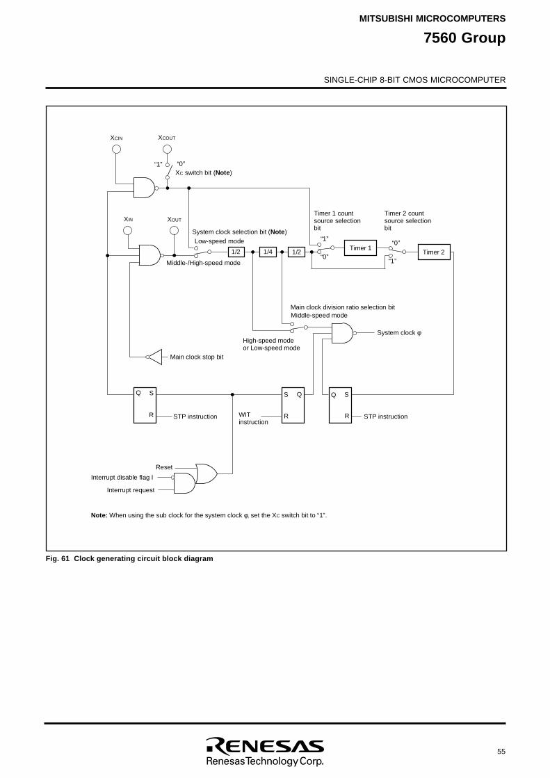
SINGLE-CHIP 8-BIT CMOS MICROCOMPUTER
MITSUBISHI MICROCOMPUTERS
7560 Group
55
Fig. 61 Clock generating circuit block diagram
W
I
Ti
n
s
t
r
u
c
t
i
o
nSTP instruction
System clock φ
S
R
Q
STP instruction
S
R
Q
Main clock stop bit
S
R
Q
T
i
m
e
r
2Timer 11
/
2 1/4
XI
N XO
U
T
XC
O
U
TXCIN
I n
t
e
r
r
u
p
t
r
e
q
u
e
s
t
R
e
s
e
t
T
i
m
e
r
1
c
o
u
n
ts
o
u
r
c
e
s
e
l
e
c
t
i
o
n
b
i
t
Timer 2 countsource selection bit
L
o
w
-
s
p
e
e
d
m
o
d
e
M
i
d
d
l
e
-
/
H
i
g
h
-
s
p
e
e
d
m
o
d
e
Sy
s
t
e
m
c
l
o
c
k
s
e
l
e
c
t
i
o
n
b
i
t
(N
o
t
e)
Middle-speed mode
High-speed mode or Low-speed mode
Note: When using the sub clock for the system clock φ, set the XC switch bit to “1”.
M
a
i
n
c
l
o
c
k
d
i
v
i
s
i
o
n
r
a
t
i
o
s
e
l
e
c
t
i
o
n
b
i
t
“ 1
”
“ 0
”
“ 1
”
“ 0
”
I n
t
e
r
r
u
p
t
d
i
s
a
b
l
e
f
l
a
g
I
1
/
2
XC
s
w
i
t
c
h
b
i
t
(N
o
t
e)“ 1
” “
0
”
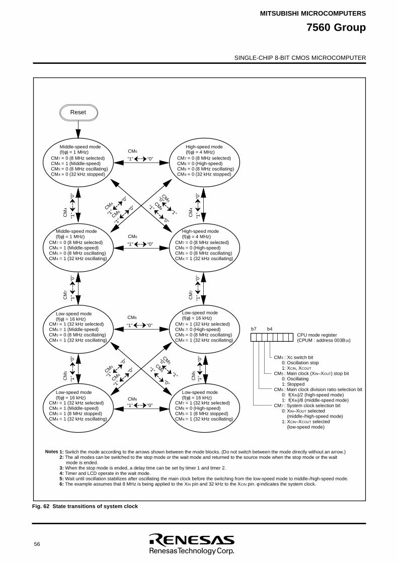
SINGLE-CHIP 8-BIT CMOS MICROCOMPUTER
MITSUBISHI MICROCOMPUTERS
7560 Group
56
Fig. 62 State transitions of system clock
N
o
t
e
s 1
:
S
w
i
t
c
h
t
h
e
m
o
d
e
a
c
c
o
r
d
i
n
g
t
o
t
h
e
a
r
r
o
w
s
s
h
o
w
n
b
e
t
w
e
e
n
t
h
e
m
o
d
e
b
l
o
c
k
s
.
(
D
o
n
o
t
s
w
i
t
c
h
b
e
t
w
e
e
n
t
h
e
m
o
d
e
d
i
r
e
c
t
l
y
w
i
t
h
o
u
t
a
n
a
r
r
o
w
.
)2
:
T
h
e
a
l
l
m
o
d
e
s
c
a
n
b
e
s
w
i
t
c
h
e
d
t
o
t
h
e
s
t
o
p
m
o
d
e
o
r
t
h
e
w
a
i
t
m
o
d
e
a
n
d
r
e
t
u
r
n
e
d
t
o
t
h
e
s
o
u
r
c
e
m
o
d
e
w
h
e
n
t
h
e
s
t
o
p
m
o
d
e
o
r
t
h
e
w
a
i
t
m
o
d
e
i
s
e
n
d
e
d
.3
:
W
h
e
n
t
h
e
s
t
o
p
m
o
d
e
i
s
e
n
d
e
d
,
a
d
e
l
a
y
t
i
m
e
c
a
n
b
e
s
e
t
b
y
t
i
m
e
r
1
a
n
d
t
i
m
e
r
2
.4:
T
i
m
e
r
a
n
d
L
C
D
o
p
e
r
a
t
e
i
n
t
h
e
w
a
i
t
m
o
d
e
.5
:
W
a
i
t
u
n
t
i
l
o
s
c
i
l
l
a
t
i
o
n
s
t
a
b
i
l
i
z
e
s
a
f
t
e
r
o
s
c
i
l
l
a
t
i
n
g
t
h
e
m
a
i
n
c
l
o
c
k
b
e
f
o
r
e
t
h
e
s
w
i
t
c
h
i
n
g
f
r
o
m
t
h
e
l
o
w
-
s
p
e
e
d
m
o
d
e
t
o
m
i
d
d
l
e
-
/
h
i
g
h
-
s
p
e
e
d
m
o
d
e
.6
:
T
h
e
e
x
a
m
p
l
e
a
s
s
u
m
e
s
t
h
a
t
8
M
H
z
i
s
b
e
i
n
g
a
p
p
l
i
e
d
t
o
t
h
e
XI
N
p
i
n
a
n
d
3
2
k
H
z
t
o
t
h
e
XC
I
N
p
i
n
.
φ
i
n
d
i
c
a
t
e
s
t
h
e
s
y
s
t
e
m
c
l
o
c
k
.
CM4 : Xc switch bit 0: Oscillation stop 1: XCIN, XCOUT
CM5 : Main clock (XIN–XOUT) stop bit 0: Oscillating 1: Stopped
CM6 : Main clock division ratio selection bit 0: f(XIN)/2 (high-speed mode) 1: f(XIN)/8 (middle-speed mode)
CM7 : System clock selection bit 0: XIN–XOUT selected (middle-/high-speed mode) 1: XCIN–XCOUT selected (low-speed mode)
CPU mode register(CPUM : address 003B16)
b
7 b4
R
e
s
e
t
CM6
“0”“1”
C
M6
“ 0
”“
1
”
C M
5
“ 0 ”
“ 1 ”
C M
5
“ 0 ”
“ 1 ”
“ 0 ”
C M5
C
M6“ 0 ”
“ 1 ”
“ 0 ”
“ 1 ”
C M
5C
M6
“ 1 ” “
1 ”
“ 0 ”
C
M6
“0”“1”
C M
7
“ 0 ”
“ 1 ”
C M
7
“ 0 ”
“ 1 ”
C
M7
=
0
(
8
M
H
z
s
e
l
e
c
t
e
d
)C
M6
=
1
(
M
i
d
d
l
e
-
s
p
e
e
d
)C
M5
=
0
(
8
M
H
z
o
s
c
i
l
l
a
t
i
n
g
)C
M4
=
0
(
3
2
k
H
z
s
t
o
p
p
e
d
)
Middle-speed mode (f(φ) = 1 MHz) C
M6
“ 0
”“
1
”
C M
4
“ 0 ”
“ 1 ”
C M
4
“ 0 ”
“ 1 ”
CM7 = 0 (8 MHz selected)CM6 = 0 (High-speed)CM5 = 0 (8 MHz oscillating)CM4 = 0 (32 kHz stopped)
High-speed mode (f(φ) = 4 MHz)
CM7 = 0 (8 MHz selected)CM6 = 1 (Middle-speed)CM5 = 0 (8 MHz oscillating)CM4 = 1 (32 kHz oscillating)
Middle-speed mode (f(φ) = 1 MHz)
CM7 = 0 (8 MHz selected)CM6 = 0 (High-speed)CM5 = 0 (8 MHz oscillating)CM4 = 1 (32 kHz oscillating)
High-speed mode (f(φ) = 4 MHz)
C M4
C
M6 “ 0 ”
“ 1 ”
“ 0 ”
“ 1 ”
C M
4C
M6
“ 1 ” “
1 ”
“ 0 ”
“ 0 ”
CM7 = 1 (32 kHz selected)CM6 = 1 (Middle-speed)CM5 = 0 (8 MHz oscillating)CM4 = 1 (32 kHz oscillating)
L
o
w-
s
p
e
e
d
m
o
d
e
(
f
(φ
)
=
1
6
k
H
z
)CM7 = 1 (32 kHz selected)CM6 = 0 (High-speed)CM5 = 0 (8 MHz oscillating)CM4 = 1 (32 kHz oscillating)
L
o
w-
s
p
e
e
d
m
o
d
e
(
f
(φ
)
=
1
6
k
H
z
)
CM7 = 1 (32 kHz selected)CM6 = 1 (Middle-speed)CM5 = 1 (8 MHz stopped)CM4 = 1 (32 kHz oscillating)
L
o
w-
s
p
e
e
d
m
o
d
e
(
f
(φ
)
=
1
6
k
H
z
)CM7 = 1 (32 kHz selected)CM6 = 0 (High-speed)CM5 = 1 (8 MHz stopped)CM4 = 1 (32 kHz oscillating)
L
o
w-
s
p
e
e
d
m
o
d
e
(
f
(φ
)
=
1
6
k
H
z
)
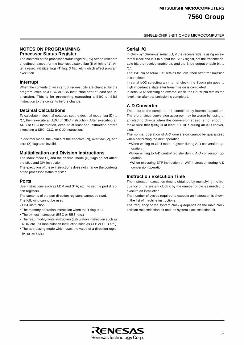
SINGLE-CHIP 8-BIT CMOS MICROCOMPUTER
MITSUBISHI MICROCOMPUTERS
7560 Group
57
NOTES ON PROGRAMMINGProcessor Status RegisterThe contents of the processor status register (PS) after a reset areundefined, except for the interrupt disable flag (I) which is “1”. Af-ter a reset, initialize flags (T flag, D flag, etc.) which affect programexecution.
InterruptWhen the contents of an interrupt request bits are changed by theprogram, execute a BBC or BBS instruction after at least one in-struction. This is for preventing executing a BBC or BBSinstruction to the contents before change.
Decimal CalculationsTo calculate in decimal notation, set the decimal mode flag (D) to“1”, then execute an ADC or SBC instruction. After executing anADC or SBC instruction, execute at least one instruction beforeexecuting a SEC, CLC, or CLD instruction.
In decimal mode, the values of the negative (N), overflow (V), andzero (Z) flags are invalid.
Multiplication and Division InstructionsThe index mode (T) and the decimal mode (D) flags do not affectthe MUL and DIV instruction.The execution of these instructions does not change the contentsof the processor status register.
PortsUse instructions such as LDM and STA, etc., to set the port direc-tion registers.The contents of the port direction registers cannot be read.The following cannot be used:• LDA instruction• The memory operation instruction when the T flag is “1”• The bit-test instruction (BBC or BBS, etc.)• The read-modify-write instruction (calculation instruction such as
ROR etc., bit manipulation instruction such as CLB or SEB etc.)• The addressing mode which uses the value of a direction regis-
ter as an index
Serial I/OIn clock synchronous serial I/O, if the receive side is using an ex-ternal clock and it is to output the SRDY signal, set the transmit en-able bit, the receive enable bit, and the SRDY output enable bit to“1”.The TxD pin of serial I/O1 retains the level then after transmissionis completed.In serial I/O2 selecting an internal clock, the SOUT2 pin goes tohigh impedance state after transmission is completed.In serial I/O2 selecting an external clock, the SOUT2 pin retains thelevel then after transmission is completed.
A-D ConverterThe input to the comparator is combined by internal capacitors.Therefore, since conversion accuracy may be worse by losing ofan electric charge when the conversion speed is not enough,make sure that f(XIN) is at least 500 kHz during an A-D conver-sion.The normal operation of A-D conversion cannot be guaranteedwhen performing the next operation:
•When writing to CPU mode register during A-D conversion op-eration
•When writing to A-D control register during A-D conversion op-eration
•When executing STP instruction or WIT instruction during A-Dconversion operation
Instruction Execution TimeThe instruction execution time is obtained by multiplying the fre-quency of the system clock φ by the number of cycles needed toexecute an instruction.The number of cycles required to execute an instruction is shownin the list of machine instructions.The frequency of the system clock φ depends on the main clockdivision ratio selection bit and the system clock selection bit.
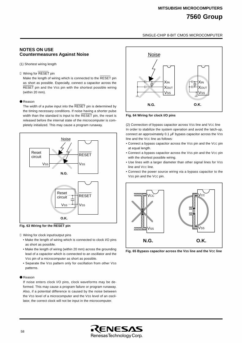
SINGLE-CHIP 8-BIT CMOS MICROCOMPUTER
MITSUBISHI MICROCOMPUTERS
7560 Group
58
NOTES ON USECountermeasures Against Noise
(1) Shortest wiring length
➀ Wiring for RESET pinMake the length of wiring which is connected to the RESET pinas short as possible. Especially, connect a capacitor across theRESET pin and the VSS pin with the shortest possible wiring(within 20 mm).
ReasonThe width of a pulse input into the RESET pin is determined bythe timing necessary conditions. If noise having a shorter pulsewidth than the standard is input to the RESET pin, the reset isreleased before the internal state of the microcomputer is com-pletely initialized. This may cause a program runaway.
Fig. 64 Wiring for clock I/O pins
(2) Connection of bypass capacitor across VSS line and VCC lineIn order to stabilize the system operation and avoid the latch-up,connect an approximately 0.1 µF bypass capacitor across the VSS
line and the VCC line as follows:• Connect a bypass capacitor across the VSS pin and the VCC pin
at equal length.• Connect a bypass capacitor across the VSS pin and the VCC pin
with the shortest possible wiring.• Use lines with a larger diameter than other signal lines for VSS
line and VCC line.• Connect the power source wiring via a bypass capacitor to the
VSS pin and the VCC pin.
Fig. 63 Wiring for the RESET pin
➁ Wiring for clock input/output pins• Make the length of wiring which is connected to clock I/O pins
as short as possible.• Make the length of wiring (within 20 mm) across the grounding
lead of a capacitor which is connected to an oscillator and theVSS pin of a microcomputer as short as possible.
• Separate the VSS pattern only for oscillation from other VSS
patterns.
ReasonIf noise enters clock I/O pins, clock waveforms may be de-formed. This may cause a program failure or program runaway.Also, if a potential difference is caused by the noise betweenthe VSS level of a microcomputer and the VSS level of an oscil-lator, the correct clock will not be input in the microcomputer.
Fig. 65 Bypass capacitor across the VSS line and the VCC line
RESETReset circuit
Noise
VSSVSS
Reset circuit
VSS
RESET
VSS
N.G.
O.K.
Noise
XIN
XOUT
VSS
XIN
XOUT
VSS
N.G. O.K.
VSS
VCC
AAAAAAAAAAAA
VSS
VCC
AAAAAAAA
AAAA
AAAAAA
N.G. O.K.
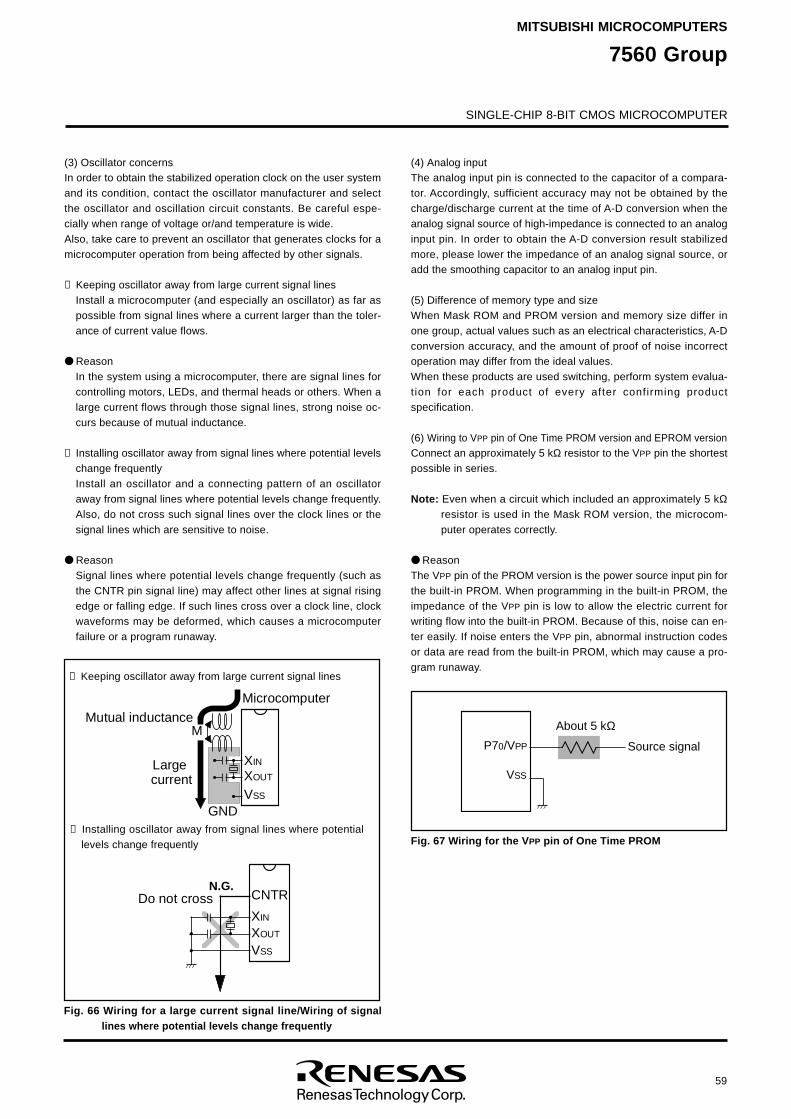
SINGLE-CHIP 8-BIT CMOS MICROCOMPUTER
MITSUBISHI MICROCOMPUTERS
7560 Group
59
(3) Oscillator concernsIn order to obtain the stabilized operation clock on the user systemand its condition, contact the oscillator manufacturer and selectthe oscillator and oscillation circuit constants. Be careful espe-cially when range of voltage or/and temperature is wide.Also, take care to prevent an oscillator that generates clocks for amicrocomputer operation from being affected by other signals.
➀ Keeping oscillator away from large current signal linesInstall a microcomputer (and especially an oscillator) as far aspossible from signal lines where a current larger than the toler-ance of current value flows.
ReasonIn the system using a microcomputer, there are signal lines forcontrolling motors, LEDs, and thermal heads or others. When alarge current flows through those signal lines, strong noise oc-curs because of mutual inductance.
➁ Installing oscillator away from signal lines where potential levelschange frequentlyInstall an oscillator and a connecting pattern of an oscillatoraway from signal lines where potential levels change frequently.Also, do not cross such signal lines over the clock lines or thesignal lines which are sensitive to noise.
ReasonSignal lines where potential levels change frequently (such asthe CNTR pin signal line) may affect other lines at signal risingedge or falling edge. If such lines cross over a clock line, clockwaveforms may be deformed, which causes a microcomputerfailure or a program runaway.
➀ Keeping oscillator away from large current signal lines
➁ Installing oscillator away from signal lines where potentiallevels change frequently Fig. 67 Wiring for the VPP pin of One Time PROM
Fig. 66 Wiring for a large current signal line/Wiring of signallines where potential levels change frequently
(4) Analog inputThe analog input pin is connected to the capacitor of a compara-tor. Accordingly, sufficient accuracy may not be obtained by thecharge/discharge current at the time of A-D conversion when theanalog signal source of high-impedance is connected to an analoginput pin. In order to obtain the A-D conversion result stabilizedmore, please lower the impedance of an analog signal source, oradd the smoothing capacitor to an analog input pin.
(5) Difference of memory type and sizeWhen Mask ROM and PROM version and memory size differ inone group, actual values such as an electrical characteristics, A-Dconversion accuracy, and the amount of proof of noise incorrectoperation may differ from the ideal values.When these products are used switching, perform system evalua-tion for each product of every after confirming productspecification.
(6) Wiring to VPP pin of One Time PROM version and EPROM versionConnect an approximately 5 kΩ resistor to the VPP pin the shortestpossible in series.
Note: Even when a circuit which included an approximately 5 kΩresistor is used in the Mask ROM version, the microcom-puter operates correctly.
ReasonThe VPP pin of the PROM version is the power source input pin forthe built-in PROM. When programming in the built-in PROM, theimpedance of the VPP pin is low to allow the electric current forwriting flow into the built-in PROM. Because of this, noise can en-ter easily. If noise enters the VPP pin, abnormal instruction codesor data are read from the built-in PROM, which may cause a pro-gram runaway.
XI
N
XO
U
T
VS
S
M
i
c
r
o
c
o
m
p
u
t
e
r
Mutual inductance
L
a
r
g
e
c
u
r
r
e
n
t
G
N
D
M
XI
N
XO
U
T
VS
S
C
N
T
RD
o
n
o
t
c
r
o
s
sN.G.
P
70/
VP
P
VSS
A
b
o
u
t
5
kΩ
S
o
u
r
c
e
s
i
g
n
a
l
SINGLE-CHIP 8-BIT CMOS MICROCOMPUTER
MITSUBISHI MICROCOMPUTERS
7560 Group
60
DATA REQUIRED FOR MASK ORDERSThe following are necessary when ordering a mask ROM produc-tion:1.Mask ROM Order Confirmation Form
2.Mark Specification Form
3.Data to be written to ROM, in EPROM form (three identical cop-ies) or one floppy disk.
For the mask ROM confirmation and the mark specifications, re-fer to the “Mitsubishi MCU Technical Information” Homepage(http://www.infomicom.maec.co.jp/indexe.htm).
Name of Programming Adapter
PCA4738F-100A
PCA4738G-100A
PCA4738L-100A
Package
100P6S-A
100P6Q-A
100D0
The PROM of the blank One Time PROM version is not tested orscreened in the assembly process and following processes. To en-sure proper operation after programming, the procedure shown inFigure 68 is recommended to verify programming.
ROM PROGRAMMING METHODThe built-in PROM of the blank One Time PROM version can beread or programmed with a general-purpose PROM programmerusing a special programming adapter. Set the address of PROMpro-grammer in the user ROM area.
Table 14 Special programming adapter
Fig. 68 State transitions of system clock
Programming with PROMprogrammer
S
c
r
e
e
n
i
n
g
(
C
a
u
t
i
o
n
)(
1
5
0
°
C
f
o
r
4
0
h
o
u
r
s
)
Verification withPROM programmer
Functional check intarget device
The screening temperature is far higherthan the storage temperature. Neverexpose to 150 °C exceeding 100 hours.
Caution :
61
SINGLE-CHIP 8-BIT CMOS MICROCOMPUTER
MITSUBISHI MICROCOMPUTERS
7560 Group
ELECTRICAL CHARACTERISTICSABSOLUTE MAXIMUM RATINGSTable 15 Absolute maximum ratings
RECOMMENDED OPERATING CONDITIONSTable 16 Recommended operating conditions (1) (VCC = 2.2 to 5.5 V, Ta = –20 to 85°C, unless otherwise noted)
Power source voltage
A-D, D-A conversion reference voltage
Analog power source voltage
Analog input voltage AN0–AN7
5.5
5.5
5.5
VCC
VCC
VCC
VSS
VREF
AVSS
VIA
Symbol ParameterLimits
Min.
V
V
V
V
V
Unit
4.0
2.2
2.2
2.0
AVSS
5.0
5.0
5.0
0
0
Typ. Max.
Power source voltage
VO
VO
VO
Pd
Topr
Tstg
–0.3 to 6.5 VPower source voltage
Input voltage P00–P07, P10–P17, P20–P27,P40–P47, P50–P57, P60–P67
Input voltage P70–P77
Input voltage VL1
Input voltage VL2
Input voltage VL3
Input voltage C1, C2
Input voltage RESET, XIN
Output voltage C1, C2
VCC
VI
Symbol Parameter Conditions Ratings Unit
All voltages are based on VSS.Output transistors are cut off.
VI
VI
VI
VI
VI
VI
VO
VO
VO
Output voltage P00–P07, P10–P15, P30–P37
Output voltage P16, P17, P20–P27, P40–P47,P50–P57, P60–P67, P71–P77
Output voltage VL3
Output voltage VL2, SEG0–SEG17
Output voltage XOUT
Power dissipationOperating temperature
Storage temperature
At output port
At segment output
Ta = 25°C
–0.3 to VCC +0.3
–0.3 to VCC +0.3
–0.3 to VL2
VL1 to VL3
VL2 to 6.5
–0.3 to 6.5
–0.3 to VCC +0.3
–0.3 to 6.5
–0.3 to VCC
–0.3 to VL3
–0.3 to VCC +0.3
–0.3 to 6.5
–0.3 to VL3
–0.3 to VCC +0.3
300–20 to 85
–40 to 125
V
V
V
V
V
V
V
V
V
V
V
V
V
V
mW
°C
°C
High-speed mode f(XIN) = 8 MHz
Middle-speed mode f(XIN) = 8 MHz
Low-speed mode
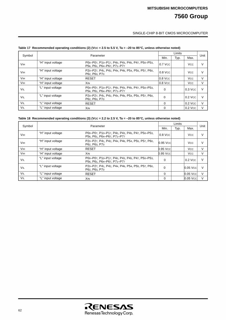
62
SINGLE-CHIP 8-BIT CMOS MICROCOMPUTER
7560 GroupMITSUBISHI MICROCOMPUTERS
V
V
“H” input voltage P00–P07, P10–P17, P40, P43, P45, P47, P50–P53,P56, P61, P64–P67, P71–P77
“H” input voltage P20–P27, P41, P42, P44, P46, P54, P55, P57, P60,P62, P63, P70
RESET
XIN
“L” input voltage P00–P07, P10–P17, P40, P43, P45, P47, P50–P53,P56, P61, P64–P67, P71–P77
“L” input voltage P20–P27, P41, P42, P44, P46, P54, P55, P57, P60,P62, P63, P70
RESET
XIN
Table 17 Recommended operating conditions (2) (VCC = 2.5 to 5.5 V, Ta = –20 to 85°C, unless otherwise noted)
Symbol ParameterLimits
Min.Unit
Typ. Max.
“H” input voltage
“H” input voltage
VIH
VIH
VIH
VIH
VIL
VIL
VIL
VIL
“L” input voltage
“L” input voltage
0.7 VCC
0.8 VCC
0.8 VCC
0.8 VCC
0
0
0
0
VCC
VCC
VCC
VCC
0.3 VCC
0.2 VCC
0.2 VCC
0.2 VCC
V
V
V
V
V
V
V
V
“H” input voltage P00–P07, P10–P17, P40, P43, P45, P47, P50–P53,P56, P61, P64–P67, P71–P77
“H” input voltage P20–P27, P41, P42, P44, P46, P54, P55, P57, P60,P62, P63, P70
RESET
XIN
“L” input voltage P00–P07, P10–P17, P40, P43, P45, P47, P50–P53,P56, P61, P64–P67, P71–P77
“L” input voltage P20–P27, P41, P42, P44, P46, P54, P55, P57, P60,P62, P63, P70
RESET
XIN
Table 18 Recommended operating conditions (3) (VCC = 2.2 to 2.5 V, Ta = –20 to 85°C, unless otherwise noted)
Symbol ParameterLimits
Min.Unit
Typ. Max.
“H” input voltage
“H” input voltage
VIH
VIH
VIH
VIH
VIL
VIL
VIL
VIL
“L” input voltage
“L” input voltage
0.8 VCC
0.95 VCC
0.95 VCC
0.95 VCC
0
0
0
0
VCC
VCC
VCC
VCC
0.2 VCC
0.05 VCC
0.05 VCC
0.05 VCC
V
V
V
V
V
V
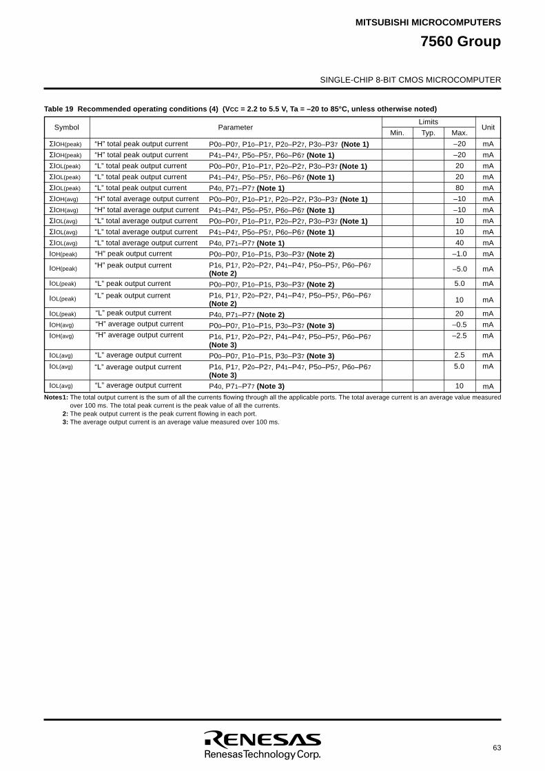
63
SINGLE-CHIP 8-BIT CMOS MICROCOMPUTER
MITSUBISHI MICROCOMPUTERS
7560 Group
P00–P07, P10–P17, P20–P27, P30–P37 (Note 1)
P41–P47, P50–P57, P60–P67 (Note 1)
P00–P07, P10–P17, P20–P27, P30–P37 (Note 1)
P41–P47, P50–P57, P60–P67 (Note 1)
P40, P71–P77 (Note 1)
P00–P07, P10–P17, P20–P27, P30–P37 (Note 1)
P41–P47, P50–P57, P60–P67 (Note 1)
P00–P07, P10–P17, P20–P27, P30–P37 (Note 1)
P41–P47, P50–P57, P60–P67 (Note 1)
P40, P71–P77 (Note 1)
P00–P07, P10–P15, P30–P37 (Note 2)
“H” peak output current P16, P17, P20–P27, P41–P47, P50–P57, P60–P67(Note 2)
P00–P07, P10–P15, P30–P37 (Note 2)
“L” peak output current P16, P17, P20–P27, P41–P47, P50–P57, P60–P67(Note 2)
P40, P71–P77 (Note 2)
P00–P07, P10–P15, P30–P37 (Note 3)
P16, P17, P20–P27, P41–P47, P50–P57, P60–P67(Note 3)
P00–P07, P10–P15, P30–P37 (Note 3)
“L” average output current P16, P17, P20–P27, P41–P47, P50–P57, P60–P67(Note 3)
P40, P71–P77 (Note 3)
–20
–20
20
20
80
–10
–10
10
10
40
–1.0
Table 19 Recommended operating conditions (4) (VCC = 2.2 to 5.5 V, Ta = –20 to 85°C, unless otherwise noted)
Notes1: The total output current is the sum of all the currents flowing through all the applicable ports. The total average current is an average value measuredover 100 ms. The total peak current is the peak value of all the currents.
2: The peak output current is the peak current flowing in each port.3: The average output current is an average value measured over 100 ms.
“H” total peak output current
“H” total peak output current
“L” total peak output current
“L” total peak output current
“L” total peak output current
“H” total average output current
“H” total average output current
“L” total average output current
“L” total average output current
“L” total average output current
ΣIOH(peak)
ΣIOH(peak)
ΣIOL(peak)
ΣIOL(peak)
ΣIOL(peak)
ΣIOH(avg)
ΣIOH(avg)
ΣIOL(avg)
ΣIOL(avg)
ΣIOL(avg)
IOH(peak)
Symbol ParameterLimits
Min.
mA
mA
mA
mA
mA
mA
mA
mA
mA
mA
mA
UnitTyp. Max.
“H” peak output current
“L” peak output current
“L” peak output current
“H” average output current
“H” average output current
“L” average output current
“L” average output current
IOH(peak)
IOL(peak)
IOL(peak)
IOL(peak)
IOH(avg)
IOH(avg)
IOL(avg)
IOL(avg)
–5.0
5.0
10
20
–0.5
–2.5
2.5
5.0
mA
mA
mA
mA
mA
mA
mA
mA
IOL(avg) mA10
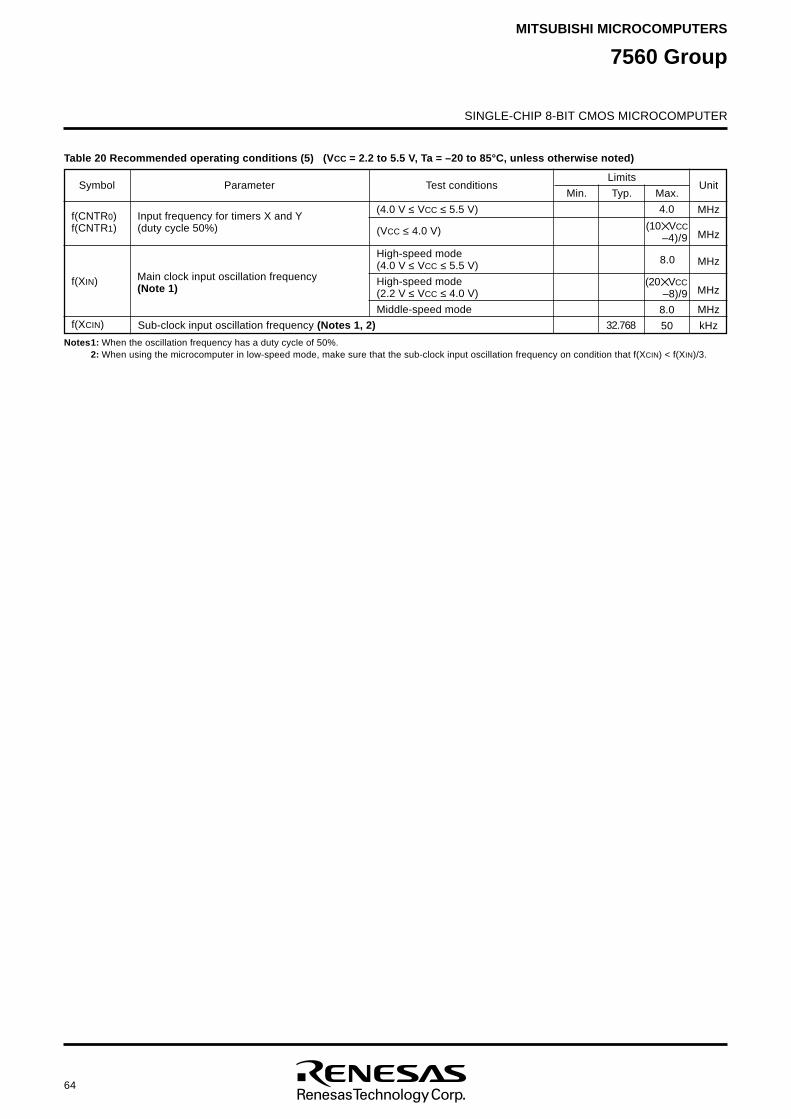
64
SINGLE-CHIP 8-BIT CMOS MICROCOMPUTER
7560 GroupMITSUBISHI MICROCOMPUTERS
Table 20 Recommended operating conditions (5) (VCC = 2.2 to 5.5 V, Ta = –20 to 85°C, unless otherwise noted)
Notes1: When the oscillation frequency has a duty cycle of 50%.2: When using the microcomputer in low-speed mode, make sure that the sub-clock input oscillation frequency on condition that f(XCIN) < f(XIN)/3.
Input frequency for timers X and Y(duty cycle 50%)
f(CNTR0)f(CNTR1)
Symbol ParameterLimits
Min.
MHz
UnitTyp. Max.
(4.0 V ≤ VCC ≤ 5.5 V)
32.768
4.0
Main clock input oscillation frequency(Note 1)
Sub-clock input oscillation frequency (Notes 1, 2)
f(XIN)
f(XCIN)
(VCC ≤ 4.0 V)
High-speed mode(4.0 V ≤ VCC ≤ 5.5 V)
High-speed mode(2.2 V ≤ VCC ≤ 4.0 V)
Middle-speed mode
(10 VCC–4)/9
8.0
(20 VCC–8)/9
8.0
50
MHz
MHz
MHz
MHz
kHz
Test conditions
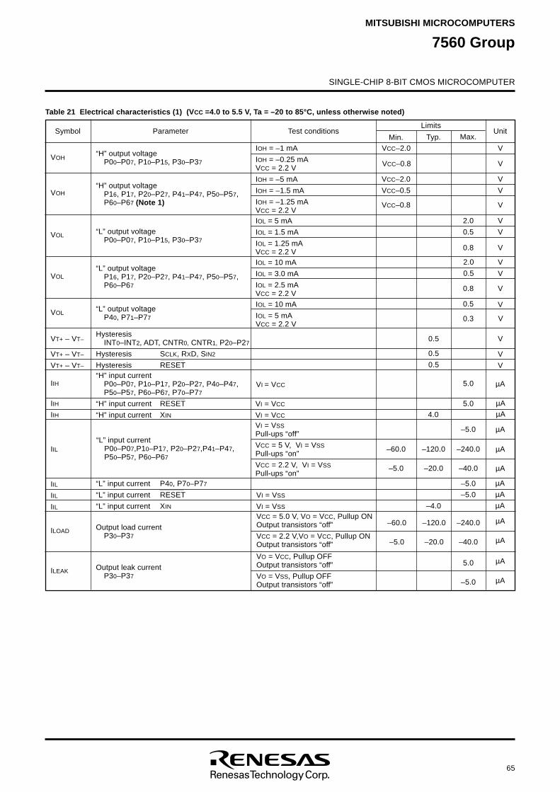
65
SINGLE-CHIP 8-BIT CMOS MICROCOMPUTER
MITSUBISHI MICROCOMPUTERS
7560 Group
VCC = 5.0 V, VO = VCC, Pullup ONOutput transistors “off”
VCC = 2.2 V,VO = VCC, Pullup ONOutput transistors “off”
IOL = 10 mA
IOL = 3.0 mA
IOL = 2.5 mAVCC = 2.2 V
IOL = 5 mA
IOL = 1.5 mA
IOL = 1.25 mAVCC = 2.2 V
VOL
IOH = –1 mA
IOH = –0.25 mAVCC = 2.2 V
IOH = –5 mA
IOH = –1.5 mA
IOH = –1.25 mAVCC = 2.2 V
VVCC–2.0“H” output voltage
P00–P07, P10–P15, P30–P37
Symbol ParameterLimits
Min.Unit
0.5
Typ. Max.Test conditions
VOH
2.0
0.5
Table 21 Electrical characteristics (1) (VCC =4.0 to 5.5 V, Ta = –20 to 85°C, unless otherwise noted)
IOL = 10 mA
IOL = 5 mAVCC = 2.2 V
VI = VCC
VI = VCC
VI = VCC
VI = VSSPull-ups “off”
VCC = 5 V, VI = VSSPull-ups “on”
VCC = 2.2 V, VI = VSSPull-ups “on”
VI = VSS
VI = VSS
“H” output voltageP16, P17, P20–P27, P41–P47, P50–P57,P60–P67 (Note 1)
“L” output voltageP00–P07, P10–P15, P30–P37
“L” output voltageP16, P17, P20–P27, P41–P47, P50–P57,P60–P67
“L” output voltageP40, P71–P77
HysteresisINT0–INT2, ADT, CNTR0, CNTR1, P20–P27
Hysteresis SCLK, RXD, SIN2
Hysteresis RESET“H” input current
P00–P07, P10–P17, P20–P27, P40–P47,P50–P57, P60–P67, P70–P77
“H” input current RESET
“H” input current XIN
“L” input currentP00–P07,P10–P17, P20–P27,P41–P47,P50–P57, P60–P67
“L” input current P40, P70–P77
“L” input current RESET
“L” input current XIN
Output load currentP30–P37
VOH
VOL
VOL
VT+ – VT–
VT+ – VT–
VT+ – VT–
IIH
IIH
IIH
IIL
IIL
IIL
ILOAD
VCC–2.0
VCC–0.5
–60.0
–5.0
0.5
0.5
4.0
–120.0
–20.0
–4.0
2.0
0.5
0.5
5.0
5.0
–5.0
–240.0
–40.0
–5.0
–5.0
–240.0
–40.0
V
V
V
V
V
V
V
V
V
V
µAµA
µA
µA
µA
µA
µA
µA
IIL
VCC–0.8
VCC–0.8
V
V
V0.8
V0.8
0.3 V
µA
µA
µA
VO = VCC, Pullup OFFOutput transistors “off”
VO = VSS, Pullup OFFOutput transistors “off”
Output leak currentP30–P37
ILEAK5.0
–5.0 µA
µA
–120.0
–20.0
–60.0
–5.0
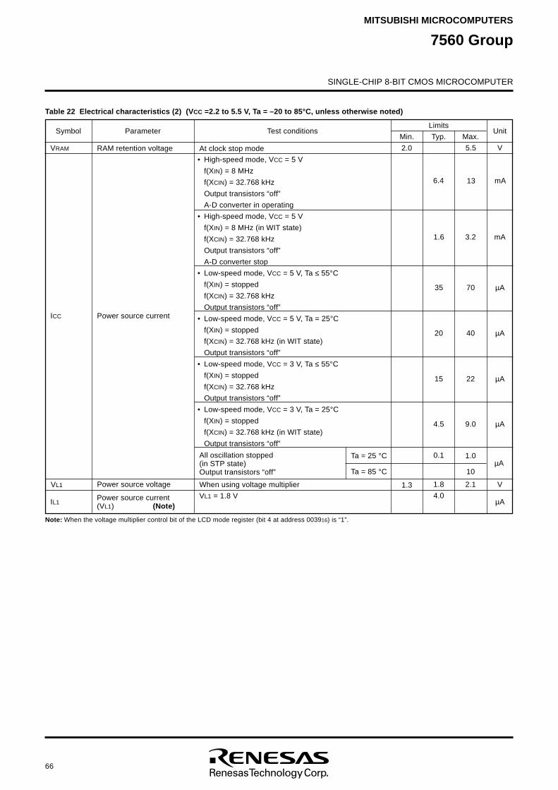
66
SINGLE-CHIP 8-BIT CMOS MICROCOMPUTER
7560 GroupMITSUBISHI MICROCOMPUTERS
Table 22 Electrical characteristics (2) (VCC =2.2 to 5.5 V, Ta = –20 to 85°C, unless otherwise noted)
V5.5
• High-speed mode, VCC = 5 V
f(XIN) = 8 MHz
f(XCIN) = 32.768 kHz
Output transistors “off”
A-D converter in operating
• High-speed mode, VCC = 5 V
f(XIN) = 8 MHz (in WIT state)
f(XCIN) = 32.768 kHz
Output transistors “off”
A-D converter stop
• Low-speed mode, VCC = 5 V, Ta ≤ 55°C
f(XIN) = stopped
f(XCIN) = 32.768 kHz
Output transistors “off”
• Low-speed mode, VCC = 5 V, Ta = 25°C
f(XIN) = stopped
f(XCIN) = 32.768 kHz (in WIT state)
Output transistors “off”
• Low-speed mode, VCC = 3 V, Ta ≤ 55°C
f(XIN) = stopped
f(XCIN) = 32.768 kHz
Output transistors “off”
• Low-speed mode, VCC = 3 V, Ta = 25°C
f(XIN) = stopped
f(XCIN) = 32.768 kHz (in WIT state)
Output transistors “off”
All oscillation stopped(in STP state)Output transistors “off”
Symbol ParameterLimits
Min.Unit
Typ. Max.
Ta = 25 °C
Ta = 85 °C
Test conditions
ICC Power source current
6.4
VRAM RAM retention voltage At clock stop mode 2.0
When using voltage multiplier
VL1 = 1.8 V
VL1
IL1
Power source voltage
Power source current(VL1) (Note)
Note: When the voltage multiplier control bit of the LCD mode register (bit 4 at address 003916) is “1”.
1.3
1.6
35
20
15
4.5
0.1
1.8
4.0
3.2
70
40
22
9.0
1.0
10
2.1
mA
µA
µA
µA
µA
µA
V
mA13
µA
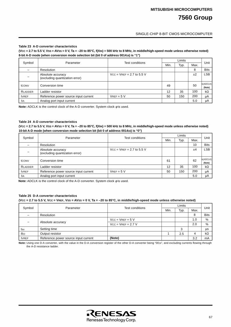
67
SINGLE-CHIP 8-BIT CMOS MICROCOMPUTER
MITSUBISHI MICROCOMPUTERS
7560 Group
Table 23 A-D converter characteristics(VCC = 2.7 to 5.5 V, VSS = AVSS = 0 V, Ta = –20 to 85°C, f(XIN) = 500 kHz to 8 MHz, in middle/high-speed mode unless otherwise noted)8-bit A-D mode (when conversion mode selection bit (bit 0 of address 001416) is “1”)
Symbol ParameterLimits
Min.Unit
Typ. Max.Test conditions
– Resolution
Absolute accuracy(excluding quantization error)
VCC = VREF = 2.7 to 5.5 V
Bits
LSB
35
150
8
±2
tc(ADCLK)
(Note)Conversion time
Ladder resistor
Reference power source input current
–
tCONV
RLADDER
IVREF
kΩµA
Table 25 D-A converter characteristics(VCC = 2.7 to 5.5 V, VCC = VREF, VSS = AVSS = 0 V, Ta = –20 to 85°C, in middle/high-speed mode unless otherwise noted)
Symbol ParameterLimits
Min.Unit
Typ. Max.Test conditions
– Resolution
VCC = VREF = 5 V
VCC = VREF = 2.7 V
1
Bits
%
%
µs
kΩmA
3
2.5
8
1.0
2.0
Note: Using one D-A converter, with the value in the D-A conversion register of the other D-A converter being “0016”, and excluding currents flowing throughthe A-D resistance ladder.
(Note)
Setting time
Output resistor
–
tsu
RO 4
3.2
12
50
Absolute accuracy
Analog port input currentIIA
IVREF Reference power source input current
µA
100
200
5.0VREF = 5 V
Table 24 A-D converter characteristics(VCC = 2.7 to 5.5 V, VSS = AVSS = 0 V, Ta = –20 to 85°C, f(XIN) = 500 kHz to 8 MHz, in middle/high-speed mode unless otherwise noted)10-bit A-D mode (when conversion mode selection bit (bit 0 of address 001416) is “0”)
49 50
Symbol ParameterLimits
Min.Unit
Typ. Max.Test conditions
– Resolution
Absolute accuracy(excluding quantization error)
VCC = VREF = 2.7 to 5.5 V
Bits
LSB
35
150
10
±4
tc(ADCLK)
(Note)Conversion time
Ladder resistor
Reference power source input current
–
tCONV
RLADDER
IVREF
kΩµA
12
50Analog port input currentIIA µA
100
200
5.0VREF = 5 V
61 62
Note: ADCLK is the control clock of the A-D converter. System clock φ is used.
Note: ADCLK is the control clock of the A-D converter. System clock φ is used.
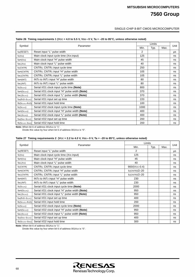
68
SINGLE-CHIP 8-BIT CMOS MICROCOMPUTER
7560 GroupMITSUBISHI MICROCOMPUTERS
Table 26 Timing requirements 1 (VCC = 4.0 to 5.5 V, VSS = 0 V, Ta = –20 to 85°C, unless otherwise noted)
2
125
45
40
250
105
105
80
80
800
370
370
220
100
1000
400
400
200
200
Note: When bit 6 of address 001A16 is “1”.Divide this value by four when bit 6 of address 001A16 is “0”.
Reset input “L” pulse width
Main clock input cycle time (XIN input)
Main clock input “H” pulse width
Main clock input “L” pulse width
CNTR0, CNTR1 input cycle time
CNTR0, CNTR1 input “H” pulse width
CNTR0, CNTR1 input “L” pulse width
INT0 to INT2 input “H” pulse width
INT0 to INT2 input “L” pulse width
Serial I/O1 clock input cycle time (Note)
Serial I/O1 clock input “H” pulse width (Note)
Serial I/O1 clock input “L” pulse width (Note)
Serial I/O1 input set up time
Serial I/O1 input hold time
Serial I/O2 clock input cycle time (Note)
Serial I/O2 clock input “H” pulse width (Note)
Serial I/O2 clock input “L” pulse width (Note)
Serial I/O2 input set up time
Serial I/O2 input hold time
tw(RESET)
tc(XIN)
twH(XIN)
twL(XIN)
tc(CNTR)
twH(CNTR)
twL(CNTR)
twH(INT)
twL(INT)
tc(SCLK1)
twH(SCLK1)
twL(SCLK1)
tsu(RXD–SCLK1)
th(SCLK1–RXD)
tc(SCLK2)
twH(SCLK2)
twL(SCLK2)
tsu(SIN2–SCLK2)
th(SCLK2–SIN2)
Symbol ParameterLimits
Min.
µs
ns
ns
ns
ns
ns
ns
ns
ns
ns
ns
ns
ns
ns
ns
ns
ns
ns
ns
UnitTyp. Max.
Table 27 Timing requirements 2 (VCC = 2.2 to 4.0 V, VSS = 0 V, Ta = –20 to 85°C, unless otherwise noted)
2
125
45
40
900/(VCC-0.4)
tc(CNTR)/2–20
tc(CNTR)/2–20
230
230
2000
950
Reset input “L” pulse width
Main clock input cycle time (XIN input)
Main clock input “H” pulse width
Main clock input “L” pulse width
CNTR0, CNTR1 input cycle time
CNTR0, CNTR1 input “H” pulse width
CNTR0, CNTR1 input “L” pulse width
INT0 to INT2 input “H” pulse width
INT0 to INT2 input “L” pulse width
Serial I/O1 clock input cycle time (Note)
Serial I/O1 clock input “H” pulse width (Note)
tw(RESET)
tc(XIN)
twH(XIN)
twL(XIN)
tc(CNTR)
twH(CNTR)
twL(CNTR)
twH(INT)
twL(INT)
tc(SCLK1)
twH(SCLK1)
Symbol ParameterLimits
Min.
µs
ns
ns
ns
ns
ns
ns
ns
ns
ns
ns
UnitTyp. Max.
Note: When bit 6 of address 001A16 is “1”.Divide this value by four when bit 6 of address 001A16 is “0”.
tsu(SIN2–SCLK2)
th(SCLK2–SIN2)
twL(SCLK1)
tsu(RXD–SCLK1)
th(SCLK1–RXD)
tc(SCLK2)
twH(SCLK2)
twL(SCLK2)
Serial I/O1 clock input “L” pulse width (Note)
Serial I/O1 input set up time
Serial I/O1 input hold time
Serial I/O2 clock input cycle time (Note)
Serial I/O2 clock input “H” pulse width (Note)
Serial I/O2 clock input “L” pulse width (Note)Serial I/O2 input set up time
Serial I/O2 input hold time
950
400
200
2000
950
950400
300
ns
ns
ns
ns
ns
nsns
ns
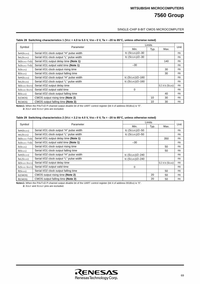
69
SINGLE-CHIP 8-BIT CMOS MICROCOMPUTER
MITSUBISHI MICROCOMPUTERS
7560 Group
Table 28 Switching characteristics 1 (VCC = 4.0 to 5.5 V, VSS = 0 V, Ta = –20 to 85°C, unless otherwise noted)
Notes1: When the P45/TXD P-channel output disable bit of the UART control register (bit 4 of address 001B16) is “0”.2: XOUT and XCOUT pins are excluded.
Serial I/O1 clock output “H” pulse width
Serial I/O1 clock output “L” pulse width
Serial I/O1 output delay time (Note 1)
Serial I/O1 output valid time (Note 1)
Serial I/O1 clock output rising time
Serial I/O1 clock output falling time
Serial I/O2 clock output “H” pulse width
Serial I/O2 clock output “L” pulse width
Serial I/O2 output delay time
Serial I/O2 output valid time
Serial I/O2 clock output falling time
CMOS output rising time (Note 2)
CMOS output falling time (Note 2)
140
30
30
0.2 tC (SCLK2)
40
30
30
Symbol ParameterLimits
Min.ns
ns
ns
ns
ns
ns
ns
ns
ns
ns
ns
ns
ns
Unit
tC (SCLK1)/2–30
tC (SCLK1)/2–30
–30
10
10
Typ. Max.
twH(SCLK1)
twL(SCLK1)
td(SCLK1–TXD)
tv(SCLK1–TXD)
tr(SCLK1)
tf(SCLK1)
twH(SCLK2)
twL(SCLK2)
td(SCLK2–SOUT2)
tv(SCLK2–SOUT2)
tf(SCLK2)
tr(CMOS)
tf(CMOS)
Table 29 Switching characteristics 2 (VCC = 2.2 to 4.0 V, VSS = 0 V, Ta = –20 to 85°C, unless otherwise noted)
ns
ns
ns
ns
ns
ns
ns
ns
ns
ns
ns
ns
ns
Unit
Notes1: When the P45/TXD P-channel output disable bit of the UART control register (bit 4 of address 001B16) is “0”.2: XOUT and XCOUT pins are excluded.
Serial I/O1 clock output “H” pulse width
Serial I/O1 clock output “L” pulse width
Serial I/O1 output delay time (Note 1)
Serial I/O1 output valid time (Note 1)
Serial I/O1 clock output rising time
Serial I/O1 clock output falling time
Serial I/O2 clock output “H” pulse width
Serial I/O2 clock output “L” pulse width
Serial I/O2 output delay time
Serial I/O2 output valid time
Serial I/O2 clock output falling time
CMOS output rising time (Note 2)
CMOS output falling time (Note 2)
350
50
50
0.2 tC (SCLK2)
50
50
50
Symbol ParameterLimits
Min.tC (SCLK1)/2–50
tC (SCLK1)/2–50
–30
20
20
Max.
twH(SCLK1)
twL(SCLK1)
td(SCLK1–TXD)
tv(SCLK1–TXD)
tr(SCLK1)
tf(SCLK1)
twH(SCLK2)
twL(SCLK2)
td(SCLK2–SOUT2)
tv(SCLK2–SOUT2)
tf(SCLK2)
tr(CMOS)
tf(CMOS)
Typ.
tC (SCLK2)/2–160
tC (SCLK2)/2–160
0
tC (SCLK2)/2–240
tC (SCLK2)/2–240
0
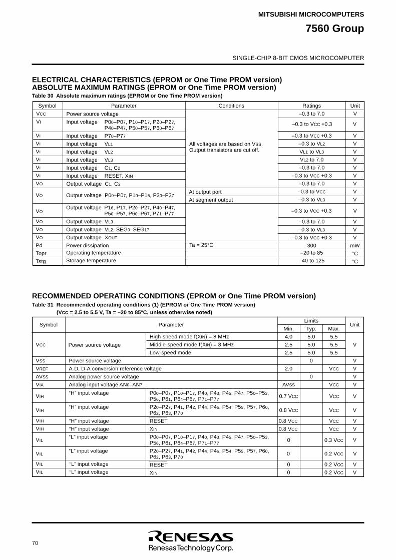
70
SINGLE-CHIP 8-BIT CMOS MICROCOMPUTER
7560 GroupMITSUBISHI MICROCOMPUTERS
V
V
“H” input voltage P00–P07, P10–P17, P40, P43, P45, P47, P50–P53,P56, P61, P64–P67, P71–P77
“H” input voltage P20–P27, P41, P42, P44, P46, P54, P55, P57, P60,P62, P63, P70
RESET
XIN
“L” input voltage P00–P07, P10–P17, P40, P43, P45, P47, P50–P53,P56, P61, P64–P67, P71–P77
“L” input voltage P20–P27, P41, P42, P44, P46, P54, P55, P57, P60,P62, P63, P70
RESET
XIN
“H” input voltage
“H” input voltage
VIH
VIH
VIH
VIH
VIL
VIL
VIL
VIL
“L” input voltage
“L” input voltage
0.7 VCC
0.8 VCC
0.8 VCC
0.8 VCC
0
0
0
0
VCC
VCC
VCC
VCC
0.3 VCC
0.2 VCC
0.2 VCC
0.2 VCC
V
V
V
V
V
V
ELECTRICAL CHARACTERISTICS (EPROM or One Time PROM version)ABSOLUTE MAXIMUM RATINGS (EPROM or One Time PROM version)Table 30 Absolute maximum ratings (EPROM or One Time PROM version)
RECOMMENDED OPERATING CONDITIONS (EPROM or One Time PROM version)Table 31 Recommended operating conditions (1) (EPROM or One Time PROM version)
(VCC = 2.5 to 5.5 V, Ta = –20 to 85°C, unless otherwise noted)
Power source voltage
A-D, D-A conversion reference voltage
Analog power source voltage
Analog input voltage AN0–AN7
5.5
5.5
5.5
VCC
VCC
VCC
VSS
VREF
AVSS
VIA
Symbol ParameterLimits
Min.
V
V
V
V
V
Unit
4.0
2.5
2.5
2.0
AVSS
5.0
5.0
5.0
0
0
Typ. Max.
Power source voltage
VO
VO
VO
Pd
Topr
Tstg
–0.3 to 7.0 VPower source voltage
Input voltage P00–P07, P10–P17, P20–P27,P40–P47, P50–P57, P60–P67
Input voltage P70–P77
Input voltage VL1
Input voltage VL2
Input voltage VL3
Input voltage C1, C2
Input voltage RESET, XIN
Output voltage C1, C2
VCC
VI
Symbol Parameter Conditions Ratings Unit
All voltages are based on VSS.Output transistors are cut off.
VI
VI
VI
VI
VI
VI
VO
VO
VO
Output voltage P00–P07, P10–P15, P30–P37
Output voltage P16, P17, P20–P27, P40–P47,P50–P57, P60–P67, P71–P77
Output voltage VL3
Output voltage VL2, SEG0–SEG17
Output voltage XOUT
Power dissipationOperating temperature
Storage temperature
At output port
At segment output
Ta = 25°C
–0.3 to VCC +0.3
–0.3 to VCC +0.3
–0.3 to VL2
VL1 to VL3
VL2 to 7.0
–0.3 to 7.0
–0.3 to VCC +0.3
–0.3 to 7.0
–0.3 to VCC
–0.3 to VL3
–0.3 to VCC +0.3
–0.3 to 7.0
–0.3 to VL3
–0.3 to VCC +0.3
300–20 to 85
–40 to 125
V
V
V
V
V
V
V
V
V
V
V
V
V
V
mW
°C
°C
High-speed mode f(XIN) = 8 MHz
Middle-speed mode f(XIN) = 8 MHz
Low-speed mode
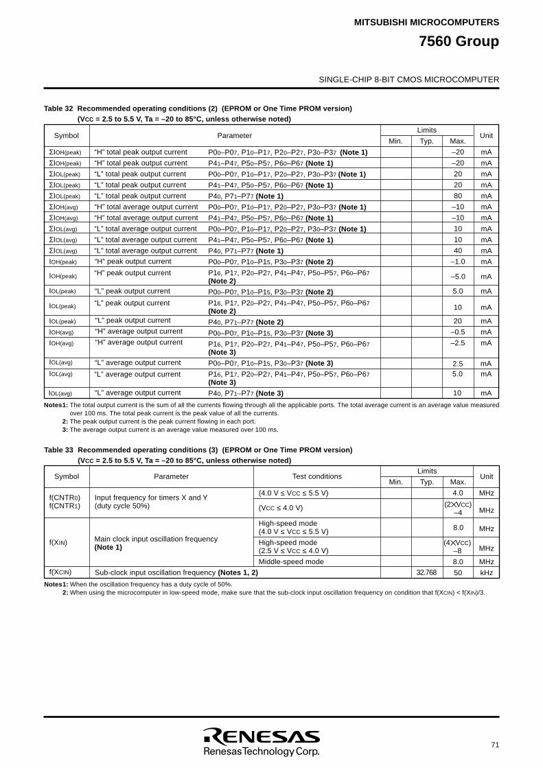
71
SINGLE-CHIP 8-BIT CMOS MICROCOMPUTER
MITSUBISHI MICROCOMPUTERS
7560 Group
P00–P07, P10–P17, P20–P27, P30–P37 (Note 1)
P41–P47, P50–P57, P60–P67 (Note 1)
P00–P07, P10–P17, P20–P27, P30–P37 (Note 1)
P41–P47, P50–P57, P60–P67 (Note 1)
P40, P71–P77 (Note 1)
P00–P07, P10–P17, P20–P27, P30–P37 (Note 1)
P41–P47, P50–P57, P60–P67 (Note 1)
P00–P07, P10–P17, P20–P27, P30–P37 (Note 1)
P41–P47, P50–P57, P60–P67 (Note 1)
P40, P71–P77 (Note 1)
P00–P07, P10–P15, P30–P37 (Note 2)
“H” peak output current P16, P17, P20–P27, P41–P47, P50–P57, P60–P67(Note 2)
P00–P07, P10–P15, P30–P37 (Note 2)
“L” peak output current P16, P17, P20–P27, P41–P47, P50–P57, P60–P67(Note 2)
P40, P71–P77 (Note 2)
P00–P07, P10–P15, P30–P37 (Note 3)
P16, P17, P20–P27, P41–P47, P50–P57, P60–P67(Note 3)
P00–P07, P10–P15, P30–P37 (Note 3)
“L” average output current P16, P17, P20–P27, P41–P47, P50–P57, P60–P67(Note 3)
P40, P71–P77 (Note 3)
–20
–20
20
20
80
–10
–10
10
10
40
–1.0
Table 32 Recommended operating conditions (2) (EPROM or One Time PROM version)(VCC = 2.5 to 5.5 V, Ta = –20 to 85°C, unless otherwise noted)
Notes1: The total output current is the sum of all the currents flowing through all the applicable ports. The total average current is an average value measuredover 100 ms. The total peak current is the peak value of all the currents.
2: The peak output current is the peak current flowing in each port.3: The average output current is an average value measured over 100 ms.
“H” total peak output current
“H” total peak output current
“L” total peak output current
“L” total peak output current
“L” total peak output current
“H” total average output current
“H” total average output current
“L” total average output current
“L” total average output current
“L” total average output current
ΣIOH(peak)
ΣIOH(peak)
ΣIOL(peak)
ΣIOL(peak)
ΣIOL(peak)
ΣIOH(avg)
ΣIOH(avg)
ΣIOL(avg)
ΣIOL(avg)
ΣIOL(avg)
IOH(peak)
Symbol ParameterLimits
Min.
mA
mA
mA
mA
mA
mA
mA
mA
mA
mA
mA
UnitTyp. Max.
“H” peak output current
“L” peak output current
“L” peak output current
“H” average output current
“H” average output current
“L” average output current
“L” average output current
IOH(peak)
IOL(peak)
IOL(peak)
IOL(peak)
IOH(avg)
IOH(avg)
IOL(avg)
IOL(avg)
–5.0
5.0
10
20
–0.5
–2.5
2.55.0
mA
mA
mA
mA
mA
mA
mAmA
Table 33 Recommended operating conditions (3) (EPROM or One Time PROM version)(VCC = 2.5 to 5.5 V, Ta = –20 to 85°C, unless otherwise noted)
Notes1: When the oscillation frequency has a duty cycle of 50%.2: When using the microcomputer in low-speed mode, make sure that the sub-clock input oscillation frequency on condition that f(XCIN) < f(XIN)/3.
Input frequency for timers X and Y(duty cycle 50%)
f(CNTR0)f(CNTR1)
Symbol ParameterLimits
Min.
MHz
UnitTyp. Max.
(4.0 V ≤ VCC ≤ 5.5 V)
32.768
4.0
Main clock input oscillation frequency(Note 1)
Sub-clock input oscillation frequency (Notes 1, 2)
f(XIN)
f(XCIN)
(VCC ≤ 4.0 V)
High-speed mode(4.0 V ≤ VCC ≤ 5.5 V)
High-speed mode(2.5 V ≤ VCC ≤ 4.0 V)
Middle-speed mode
(2 VCC)–4
8.0
(4 VCC)–8
8.0
50
MHz
MHz
MHz
MHz
kHz
Test conditions
IOL(avg) 10 mA
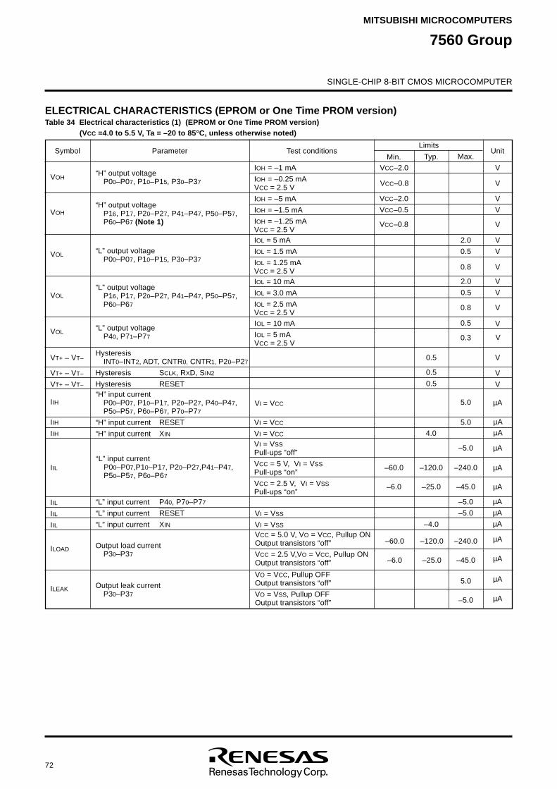
72
SINGLE-CHIP 8-BIT CMOS MICROCOMPUTER
7560 GroupMITSUBISHI MICROCOMPUTERS
VCC = 5.0 V, VO = VCC, Pullup ONOutput transistors “off”
VCC = 2.5 V,VO = VCC, Pullup ONOutput transistors “off”
IOL = 10 mA
IOL = 3.0 mA
IOL = 2.5 mAVCC = 2.5 V
IOL = 5 mA
IOL = 1.5 mA
IOL = 1.25 mAVCC = 2.5 V
VOL
IOH = –1 mA
IOH = –0.25 mAVCC = 2.5 V
IOH = –5 mA
IOH = –1.5 mA
IOH = –1.25 mAVCC = 2.5 V
VVCC–2.0“H” output voltage
P00–P07, P10–P15, P30–P37
Symbol ParameterLimits
Min.Unit
0.5
Typ. Max.Test conditions
VOH
2.0
0.5
ELECTRICAL CHARACTERISTICS (EPROM or One Time PROM version)Table 34 Electrical characteristics (1) (EPROM or One Time PROM version)
(VCC =4.0 to 5.5 V, Ta = –20 to 85°C, unless otherwise noted)
IOL = 10 mA
IOL = 5 mAVCC = 2.5 V
VI = VCC
VI = VCC
VI = VCC
VI = VSSPull-ups “off”
VCC = 5 V, VI = VSSPull-ups “on”
VCC = 2.5 V, VI = VSSPull-ups “on”
VI = VSS
VI = VSS
“H” output voltageP16, P17, P20–P27, P41–P47, P50–P57,P60–P67 (Note 1)
“L” output voltageP00–P07, P10–P15, P30–P37
“L” output voltageP16, P17, P20–P27, P41–P47, P50–P57,P60–P67
“L” output voltageP40, P71–P77
HysteresisINT0–INT2, ADT, CNTR0, CNTR1, P20–P27
Hysteresis SCLK, RXD, SIN2
Hysteresis RESET“H” input current
P00–P07, P10–P17, P20–P27, P40–P47,P50–P57, P60–P67, P70–P77
“H” input current RESET
“H” input current XIN
“L” input currentP00–P07,P10–P17, P20–P27,P41–P47,P50–P57, P60–P67
“L” input current P40, P70–P77
“L” input current RESET
“L” input current XIN
Output load currentP30–P37
VOH
VOL
VOL
VT+ – VT–
VT+ – VT–
VT+ – VT–
IIH
IIH
IIH
IIL
IIL
IIL
ILOAD
VCC–2.0
VCC–0.5
–60.0
–6.0
0.5
0.5
4.0
–120.0
–25.0
–4.0
2.0
0.5
0.5
5.0
5.0
–5.0
–240.0
–45.0
–5.0
–5.0
–240.0
–45.0
V
V
V
V
V
V
V
V
V
V
µA
µA
µA
µA
µA
µA
µA
µA
IIL
VCC–0.8
VCC–0.8
V
V
V0.8
V0.8
0.3 V
µA
µA
µA
VO = VCC, Pullup OFFOutput transistors “off”
VO = VSS, Pullup OFFOutput transistors “off”
Output leak currentP30–P37
ILEAK5.0
–5.0 µA
µA
–120.0
–25.0
–60.0
–6.0
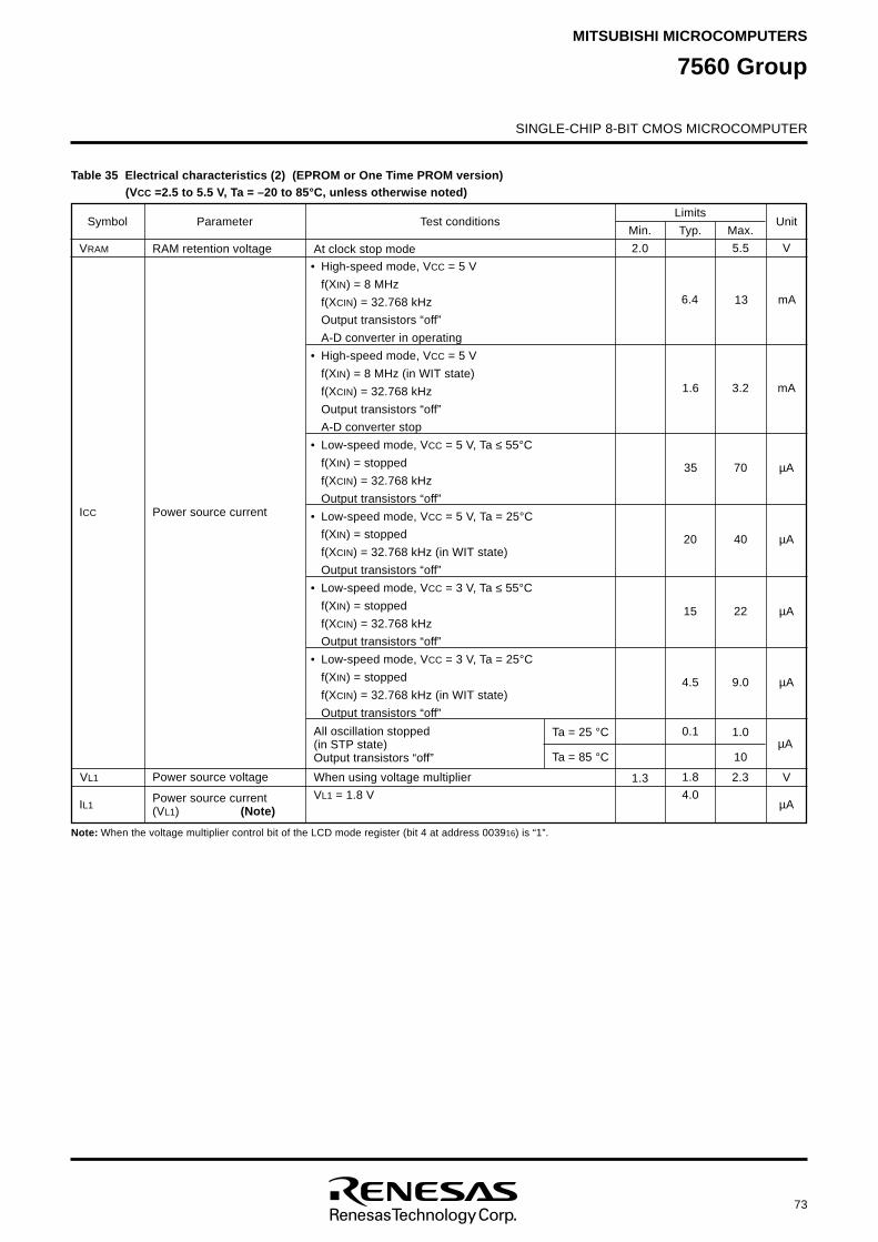
73
SINGLE-CHIP 8-BIT CMOS MICROCOMPUTER
MITSUBISHI MICROCOMPUTERS
7560 Group
Table 35 Electrical characteristics (2) (EPROM or One Time PROM version)(VCC =2.5 to 5.5 V, Ta = –20 to 85°C, unless otherwise noted)
V5.5
• High-speed mode, VCC = 5 V
f(XIN) = 8 MHz
f(XCIN) = 32.768 kHz
Output transistors “off”
A-D converter in operating
• High-speed mode, VCC = 5 V
f(XIN) = 8 MHz (in WIT state)
f(XCIN) = 32.768 kHz
Output transistors “off”
A-D converter stop
• Low-speed mode, VCC = 5 V, Ta ≤ 55°C
f(XIN) = stopped
f(XCIN) = 32.768 kHz
Output transistors “off”
• Low-speed mode, VCC = 5 V, Ta = 25°C
f(XIN) = stopped
f(XCIN) = 32.768 kHz (in WIT state)
Output transistors “off”
• Low-speed mode, VCC = 3 V, Ta ≤ 55°C
f(XIN) = stopped
f(XCIN) = 32.768 kHz
Output transistors “off”
• Low-speed mode, VCC = 3 V, Ta = 25°C
f(XIN) = stopped
f(XCIN) = 32.768 kHz (in WIT state)
Output transistors “off”
All oscillation stopped(in STP state)Output transistors “off”
Symbol ParameterLimits
Min.Unit
Typ. Max.
Ta = 25 °C
Ta = 85 °C
Test conditions
ICC Power source current
6.4
VRAM RAM retention voltage At clock stop mode 2.0
When using voltage multiplier
VL1 = 1.8 V
VL1
IL1
Power source voltage
Power source current(VL1) (Note)
Note: When the voltage multiplier control bit of the LCD mode register (bit 4 at address 003916) is “1”.
1.3
1.6
35
20
15
4.5
0.1
1.8
4.0
3.2
70
40
22
9.0
1.0
10
2.3
mA
µA
µA
µA
µA
µA
V
mA13
µA
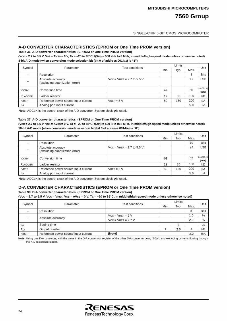
74
SINGLE-CHIP 8-BIT CMOS MICROCOMPUTER
7560 GroupMITSUBISHI MICROCOMPUTERS
A-D CONVERTER CHARACTERISTICS (EPROM or One Time PROM version)Table 36 A-D converter characteristics (EPROM or One Time PROM version)(VCC = 2.7 to 5.5 V, VSS = AVSS = 0 V, Ta = –20 to 85°C, f(XIN) = 500 kHz to 8 MHz, in middle/high-speed mode unless otherwise noted)8-bit A-D mode (when conversion mode selection bit (bit 0 of address 001416) is “1”)
Symbol ParameterLimits
Min.Unit
Typ. Max.Test conditions
– Resolution
Absolute accuracy(excluding quantization error)
VCC = VREF = 2.7 to 5.5 V
Bits
LSB
35
150
8
±2
tc(ADCLK)
(Note)Conversion time
Ladder resistor
Reference power source input current
–
tCONV
RLADDER
IVREF
kΩµA
D-A CONVERTER CHARACTERISTICS (EPROM or One Time PROM version)Table 38 D-A converter characteristics (EPROM or One Time PROM version)(VCC = 2.7 to 5.5 V, VCC = VREF, VSS = AVSS = 0 V, Ta = –20 to 85°C, in middle/high-speed mode unless otherwise noted)
Symbol ParameterLimits
Min.Unit
Typ. Max.Test conditions
– Resolution
VCC = VREF = 5 V
VCC = VREF = 2.7 V
1
Bits
%
%
µs
kΩmA
3
2.5
8
1.0
2.0
Note: Using one D-A converter, with the value in the D-A conversion register of the other D-A converter being “0016”, and excluding currents flowing throughthe A-D resistance ladder.
(Note)
Setting time
Output resistor
–
tsu
RO 4
3.2
12
50
Absolute accuracy
Analog port input currentIIA
IVREF Reference power source input current
µA
100
200
5.0VREF = 5 V
Table 37 A-D converter characteristics (EPROM or One Time PROM version)(VCC = 2.7 to 5.5 V, VSS = AVSS = 0 V, Ta = –20 to 85°C, f(XIN) = 500 kHz to 8 MHz, in middle/high-speed mode unless otherwise noted)10-bit A-D mode (when conversion mode selection bit (bit 0 of address 001416) is “0”)
49 50
Symbol ParameterLimits
Min.Unit
Typ. Max.Test conditions
– Resolution
Absolute accuracy(excluding quantization error)
VCC = VREF = 2.7 to 5.5 V
Bits
LSB
35
150
10
±4
tc(ADCLK)
(Note)Conversion time
Ladder resistor
Reference power source input current
–
tCONV
RLADDER
IVREF
kΩµA
12
50Analog port input currentIIA µA
100
200
5.0VREF = 5 V
61 62
Note: ADCLK is the control clock of the A-D converter. System clock φ is used.
Note: ADCLK is the control clock of the A-D converter. System clock φ is used.
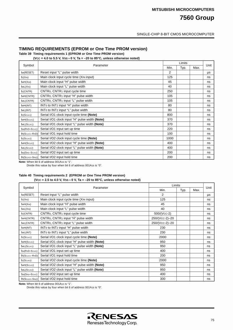
75
SINGLE-CHIP 8-BIT CMOS MICROCOMPUTER
MITSUBISHI MICROCOMPUTERS
7560 Group
TIMING REQUIREMENTS (EPROM or One Time PROM version)Table 39 Timing requirements 1 (EPROM or One Time PROM version)
(VCC = 4.0 to 5.5 V, VSS = 0 V, Ta = –20 to 85°C, unless otherwise noted)
2
125
45
40
250
105
105
80
80
800
370
370
220
100
1000
400
400
200
200
Note: When bit 6 of address 001A16 is “1”.Divide this value by four when bit 6 of address 001A16 is “0”.
Reset input “L” pulse width
Main clock input cycle time (XIN input)
Main clock input “H” pulse width
Main clock input “L” pulse width
CNTR0, CNTR1 input cycle time
CNTR0, CNTR1 input “H” pulse width
CNTR0, CNTR1 input “L” pulse width
INT0 to INT2 input “H” pulse width
INT0 to INT2 input “L” pulse width
Serial I/O1 clock input cycle time (Note)
Serial I/O1 clock input “H” pulse width (Note)
Serial I/O1 clock input “L” pulse width (Note)
Serial I/O1 input set up time
Serial I/O1 input hold time
Serial I/O2 clock input cycle time (Note)
Serial I/O2 clock input “H” pulse width (Note)
Serial I/O2 clock input “L” pulse width (Note)
Serial I/O2 input set up time
Serial I/O2 input hold time
tw(RESET)
tc(XIN)
twH(XIN)
twL(XIN)
tc(CNTR)
twH(CNTR)
twL(CNTR)
twH(INT)
twL(INT)
tc(SCLK1)
twH(SCLK1)
twL(SCLK1)
tsu(RXD–SCLK1)
th(SCLK1–RXD)
tc(SCLK2)
twH(SCLK2)
twL(SCLK2)
tsu(SIN2–SCLK2)
th(SCLK2–SIN2)
Symbol ParameterLimits
Min.
µs
ns
ns
ns
ns
ns
ns
ns
ns
ns
ns
ns
ns
ns
ns
ns
ns
ns
ns
UnitTyp. Max.
Table 40 Timing requirements 2 (EPROM or One Time PROM version) (VCC = 2.5 to 4.0 V, VSS = 0 V, Ta = –20 to 85°C, unless otherwise noted)
2
125
45
40
500/(VCC-2)
250/(VCC-2)–20
250/(VCC-2)–20
230
230
2000
950
Reset input “L” pulse width
Main clock input cycle time (XIN input)
Main clock input “H” pulse width
Main clock input “L” pulse width
CNTR0, CNTR1 input cycle time
CNTR0, CNTR1 input “H” pulse width
CNTR0, CNTR1 input “L” pulse width
INT0 to INT2 input “H” pulse width
INT0 to INT2 input “L” pulse width
Serial I/O1 clock input cycle time (Note)
Serial I/O1 clock input “H” pulse width (Note)
tw(RESET)
tc(XIN)
twH(XIN)
twL(XIN)
tc(CNTR)
twH(CNTR)
twL(CNTR)
twH(INT)
twL(INT)
tc(SCLK1)
twH(SCLK1)
Symbol ParameterLimits
Min.
µs
ns
ns
ns
ns
ns
ns
ns
ns
ns
ns
UnitTyp. Max.
Note: When bit 6 of address 001A16 is “1”.Divide this value by four when bit 6 of address 001A16 is “0”.
tsu(SIN2–SCLK2)
th(SCLK2–SIN2)
twL(SCLK1)
tsu(RXD–SCLK1)
th(SCLK1–RXD)
tc(SCLK2)
twH(SCLK2)
twL(SCLK2)
Serial I/O1 clock input “L” pulse width (Note)
Serial I/O1 input set up time
Serial I/O1 input hold time
Serial I/O2 clock input cycle time (Note)
Serial I/O2 clock input “H” pulse width (Note)
Serial I/O2 clock input “L” pulse width (Note)Serial I/O2 input set up time
Serial I/O2 input hold time
950
400
200
2000
950
950400
300
ns
ns
ns
ns
ns
nsns
ns
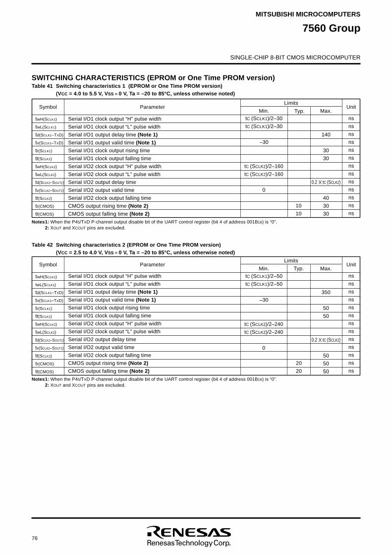
76
SINGLE-CHIP 8-BIT CMOS MICROCOMPUTER
7560 GroupMITSUBISHI MICROCOMPUTERS
SWITCHING CHARACTERISTICS (EPROM or One Time PROM version)Table 41 Switching characteristics 1 (EPROM or One Time PROM version)
(VCC = 4.0 to 5.5 V, VSS = 0 V, Ta = –20 to 85°C, unless otherwise noted)
Notes1: When the P45/TXD P-channel output disable bit of the UART control register (bit 4 of address 001B16) is “0”.2: XOUT and XCOUT pins are excluded.
Serial I/O1 clock output “H” pulse width
Serial I/O1 clock output “L” pulse width
Serial I/O1 output delay time (Note 1)
Serial I/O1 output valid time (Note 1)
Serial I/O1 clock output rising time
Serial I/O1 clock output falling time
Serial I/O2 clock output “H” pulse width
Serial I/O2 clock output “L” pulse width
Serial I/O2 output delay time
Serial I/O2 output valid time
Serial I/O2 clock output falling time
CMOS output rising time (Note 2)
CMOS output falling time (Note 2)
140
30
30
0.2 tC (SCLK2)
40
30
30
Symbol ParameterLimits
Min.ns
ns
ns
ns
ns
ns
ns
ns
ns
ns
ns
ns
ns
Unit
tC (SCLK1)/2–30
tC (SCLK1)/2–30
–30
10
10
Typ. Max.
twH(SCLK1)
twL(SCLK1)
td(SCLK1–TXD)
tv(SCLK1–TXD)
tr(SCLK1)
tf(SCLK1)
twH(SCLK2)
twL(SCLK2)
td(SCLK2–SOUT2)
tv(SCLK2–SOUT2)
tf(SCLK2)
tr(CMOS)
tf(CMOS)
Table 42 Switching characteristics 2 (EPROM or One Time PROM version)(VCC = 2.5 to 4.0 V, VSS = 0 V, Ta = –20 to 85°C, unless otherwise noted)
ns
ns
ns
ns
ns
ns
ns
ns
ns
ns
ns
ns
ns
Unit
Notes1: When the P45/TXD P-channel output disable bit of the UART control register (bit 4 of address 001B16) is “0”.2: XOUT and XCOUT pins are excluded.
Serial I/O1 clock output “H” pulse width
Serial I/O1 clock output “L” pulse width
Serial I/O1 output delay time (Note 1)
Serial I/O1 output valid time (Note 1)
Serial I/O1 clock output rising time
Serial I/O1 clock output falling time
Serial I/O2 clock output “H” pulse width
Serial I/O2 clock output “L” pulse width
Serial I/O2 output delay time
Serial I/O2 output valid time
Serial I/O2 clock output falling time
CMOS output rising time (Note 2)
CMOS output falling time (Note 2)
350
50
50
0.2 tC (SCLK2)
50
50
50
Symbol ParameterLimits
Min.tC (SCLK1)/2–50
tC (SCLK1)/2–50
–30
20
20
Max.
twH(SCLK1)
twL(SCLK1)
td(SCLK1–TXD)
tv(SCLK1–TXD)
tr(SCLK1)
tf(SCLK1)
twH(SCLK2)
twL(SCLK2)
td(SCLK2–SOUT2)
tv(SCLK2–SOUT2)
tf(SCLK2)
tr(CMOS)
tf(CMOS)
Typ.
tC (SCLK2)/2–160
tC (SCLK2)/2–160
0
tC (SCLK2)/2–240
tC (SCLK2)/2–240
0
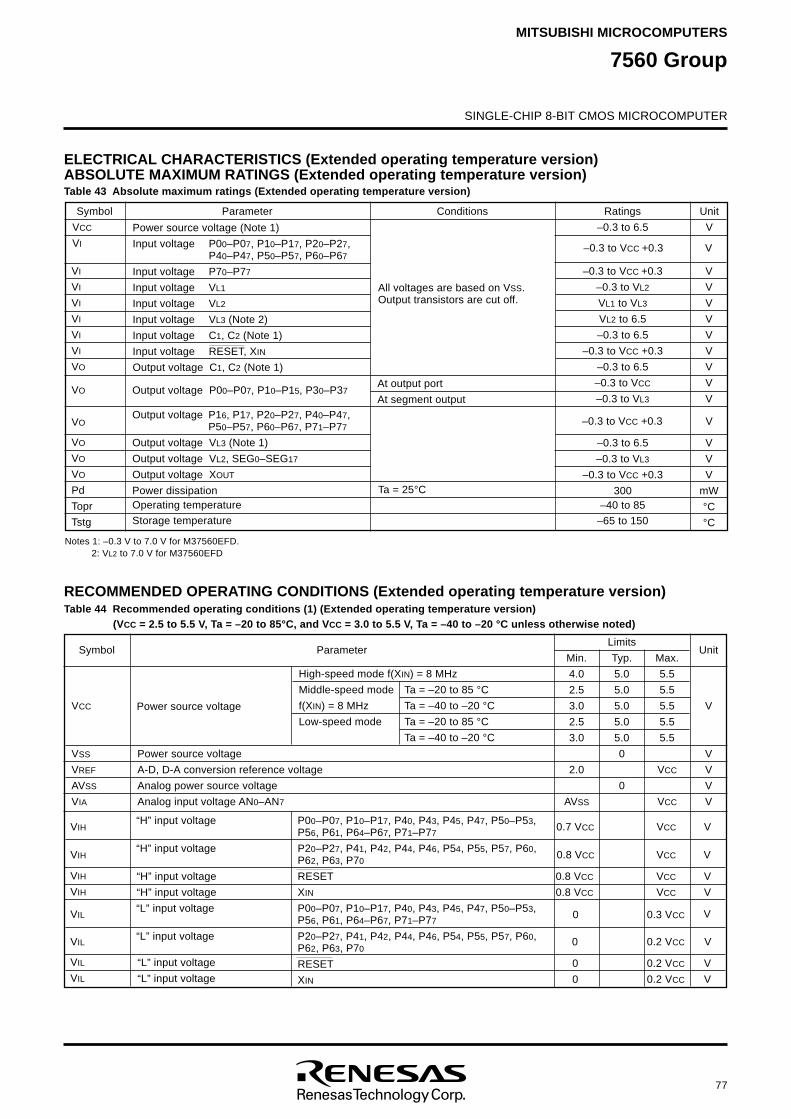
77
SINGLE-CHIP 8-BIT CMOS MICROCOMPUTER
MITSUBISHI MICROCOMPUTERS
7560 Group
ELECTRICAL CHARACTERISTICS (Extended operating temperature version)ABSOLUTE MAXIMUM RATINGS (Extended operating temperature version)Table 43 Absolute maximum ratings (Extended operating temperature version)
RECOMMENDED OPERATING CONDITIONS (Extended operating temperature version)Table 44 Recommended operating conditions (1) (Extended operating temperature version)
(VCC = 2.5 to 5.5 V, Ta = –20 to 85°C, and VCC = 3.0 to 5.5 V, Ta = –40 to –20 °C unless otherwise noted)
Power source voltage
A-D, D-A conversion reference voltage
Analog power source voltage
Analog input voltage AN0–AN7
5.5
5.5
5.5
5.5
5.5
VCC
VCC
VCC
VSS
VREF
AVSS
VIA
Symbol ParameterLimits
Min.
V
V
V
V
V
Unit
4.0
2.5
3.0
2.5
3.0
2.0
AVSS
5.0
5.0
5.0
5.0
5.0
0
0
Typ. Max.
Power source voltage
VO
VO
VO
Pd
Topr
Tstg
–0.3 to 6.5 VPower source voltage (Note 1)
Input voltage P00–P07, P10–P17, P20–P27,P40–P47, P50–P57, P60–P67
Input voltage P70–P77
Input voltage VL1
Input voltage VL2
Input voltage VL3 (Note 2)
Input voltage C1, C2 (Note 1)
Input voltage RESET, XIN
Output voltage C1, C2 (Note 1)
VCC
VI
Symbol Parameter Conditions Ratings Unit
All voltages are based on VSS.Output transistors are cut off.
VI
VI
VI
VI
VI
VI
VO
VO
VO
Output voltage P00–P07, P10–P15, P30–P37
Output voltage P16, P17, P20–P27, P40–P47,P50–P57, P60–P67, P71–P77
Output voltage VL3 (Note 1)
Output voltage VL2, SEG0–SEG17
Output voltage XOUT
Power dissipationOperating temperature
Storage temperature
At output port
At segment output
Ta = 25°C
–0.3 to VCC +0.3
–0.3 to VCC +0.3
–0.3 to VL2
VL1 to VL3
VL2 to 6.5
–0.3 to 6.5
–0.3 to VCC +0.3
–0.3 to 6.5
–0.3 to VCC
–0.3 to VL3
–0.3 to VCC +0.3
–0.3 to 6.5
–0.3 to VL3
–0.3 to VCC +0.3
300–40 to 85
–65 to 150
V
V
V
V
V
V
V
V
V
V
V
V
V
V
mW
°C
°C
High-speed mode f(XIN) = 8 MHz
Middle-speed mode Ta = –20 to 85 °C
f(XIN) = 8 MHz Ta = –40 to –20 °C
Low-speed mode Ta = –20 to 85 °C
Ta = –40 to –20 °C
Notes 1: –0.3 V to 7.0 V for M37560EFD.2: VL2 to 7.0 V for M37560EFD
V
V
“H” input voltage P00–P07, P10–P17, P40, P43, P45, P47, P50–P53,P56, P61, P64–P67, P71–P77
“H” input voltage P20–P27, P41, P42, P44, P46, P54, P55, P57, P60,P62, P63, P70
RESET
XIN
“L” input voltage P00–P07, P10–P17, P40, P43, P45, P47, P50–P53,P56, P61, P64–P67, P71–P77
“L” input voltage P20–P27, P41, P42, P44, P46, P54, P55, P57, P60,P62, P63, P70
RESET
XIN
“H” input voltage
“H” input voltage
VIH
VIH
VIH
VIH
VIL
VIL
VIL
VIL
“L” input voltage
“L” input voltage
0.7 VCC
0.8 VCC
0.8 VCC
0.8 VCC
0
0
0
0
VCC
VCC
VCC
VCC
0.3 VCC
0.2 VCC
0.2 VCC
0.2 VCC
V
V
V
V
V
V
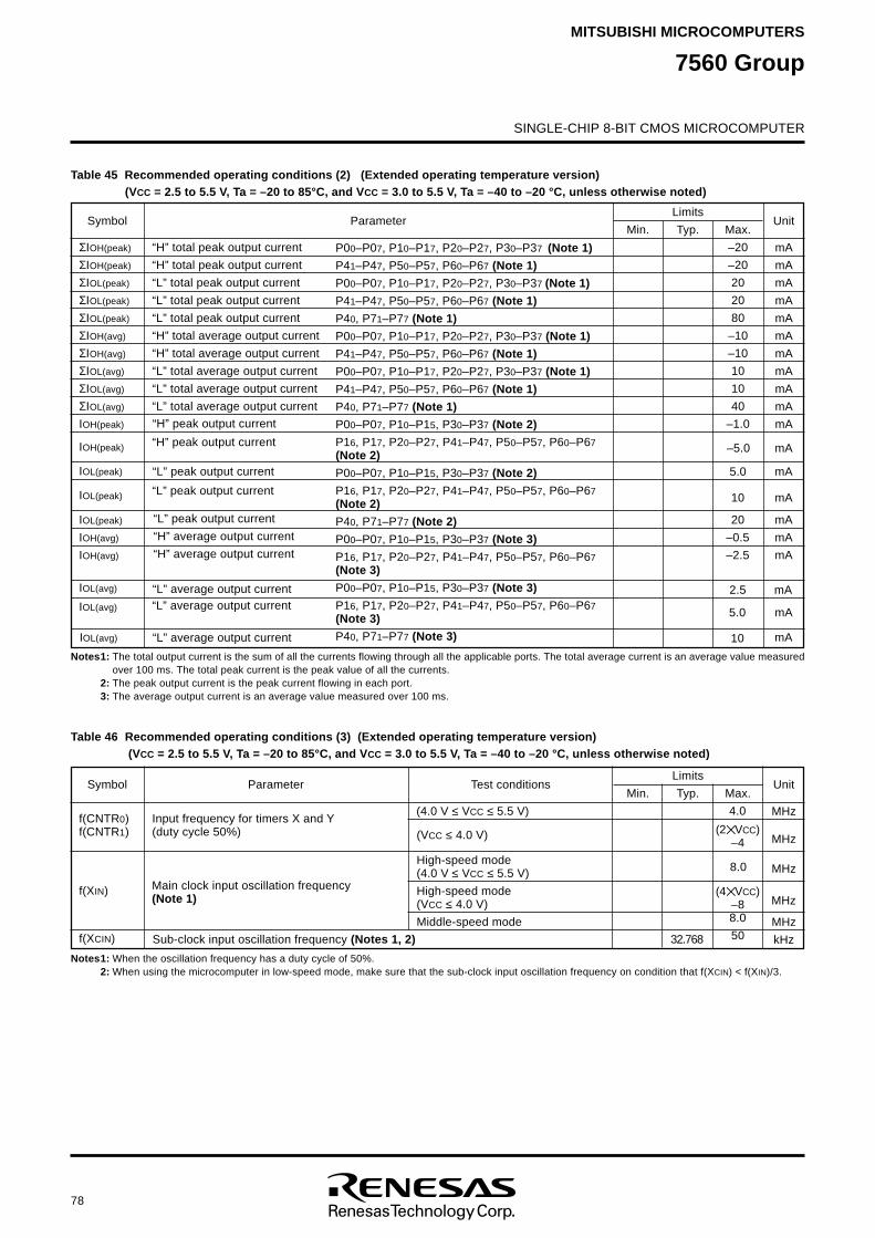
78
SINGLE-CHIP 8-BIT CMOS MICROCOMPUTER
7560 GroupMITSUBISHI MICROCOMPUTERS
P00–P07, P10–P17, P20–P27, P30–P37 (Note 1)
P41–P47, P50–P57, P60–P67 (Note 1)
P00–P07, P10–P17, P20–P27, P30–P37 (Note 1)
P41–P47, P50–P57, P60–P67 (Note 1)
P40, P71–P77 (Note 1)
P00–P07, P10–P17, P20–P27, P30–P37 (Note 1)
P41–P47, P50–P57, P60–P67 (Note 1)
P00–P07, P10–P17, P20–P27, P30–P37 (Note 1)
P41–P47, P50–P57, P60–P67 (Note 1)
P40, P71–P77 (Note 1)
P00–P07, P10–P15, P30–P37 (Note 2)
“H” peak output current P16, P17, P20–P27, P41–P47, P50–P57, P60–P67(Note 2)
P00–P07, P10–P15, P30–P37 (Note 2)
“L” peak output current P16, P17, P20–P27, P41–P47, P50–P57, P60–P67(Note 2)
P40, P71–P77 (Note 2)
P00–P07, P10–P15, P30–P37 (Note 3)
P16, P17, P20–P27, P41–P47, P50–P57, P60–P67(Note 3)
P00–P07, P10–P15, P30–P37 (Note 3)
“L” average output current P16, P17, P20–P27, P41–P47, P50–P57, P60–P67(Note 3)
P40, P71–P77 (Note 3)
–20
–20
20
20
80
–10
–10
10
10
40
–1.0
Table 45 Recommended operating conditions (2) (Extended operating temperature version)(VCC = 2.5 to 5.5 V, Ta = –20 to 85°C, and VCC = 3.0 to 5.5 V, Ta = –40 to –20 °C, unless otherwise noted)
Notes1: The total output current is the sum of all the currents flowing through all the applicable ports. The total average current is an average value measuredover 100 ms. The total peak current is the peak value of all the currents.
2: The peak output current is the peak current flowing in each port.3: The average output current is an average value measured over 100 ms.
“H” total peak output current
“H” total peak output current
“L” total peak output current
“L” total peak output current
“L” total peak output current
“H” total average output current
“H” total average output current
“L” total average output current
“L” total average output current
“L” total average output current
ΣIOH(peak)
ΣIOH(peak)
ΣIOL(peak)
ΣIOL(peak)
ΣIOL(peak)
ΣIOH(avg)
ΣIOH(avg)
ΣIOL(avg)
ΣIOL(avg)
ΣIOL(avg)
IOH(peak)
Symbol ParameterLimits
Min.
mA
mA
mA
mA
mA
mA
mA
mA
mA
mA
mA
UnitTyp. Max.
“H” peak output current
“L” peak output current
“L” peak output current
“H” average output current
“H” average output current
“L” average output current
“L” average output current
IOH(peak)
IOL(peak)
IOL(peak)
IOL(peak)
IOH(avg)
IOH(avg)
IOL(avg)
IOL(avg)
–5.0
5.0
10
20
–0.5
–2.5
2.5
5.0
mA
mA
mA
mA
mA
mA
mA
mA
Table 46 Recommended operating conditions (3) (Extended operating temperature version) (VCC = 2.5 to 5.5 V, Ta = –20 to 85°C, and VCC = 3.0 to 5.5 V, Ta = –40 to –20 °C, unless otherwise noted)
Notes1: When the oscillation frequency has a duty cycle of 50%.2: When using the microcomputer in low-speed mode, make sure that the sub-clock input oscillation frequency on condition that f(XCIN) < f(XIN)/3.
Input frequency for timers X and Y(duty cycle 50%)
f(CNTR0)f(CNTR1)
Symbol ParameterLimits
Min.
MHz
UnitTyp. Max.
(4.0 V ≤ VCC ≤ 5.5 V)
32.768
4.0
Main clock input oscillation frequency(Note 1)
Sub-clock input oscillation frequency (Notes 1, 2)
f(XIN)
f(XCIN)
(VCC ≤ 4.0 V)
High-speed mode(4.0 V ≤ VCC ≤ 5.5 V)
High-speed mode(VCC ≤ 4.0 V)
Middle-speed mode
(2 VCC)–4
8.0
(4 VCC)–88.0
50
MHz
MHz
MHz
MHz
kHz
Test conditions
IOL(avg) 10 mA
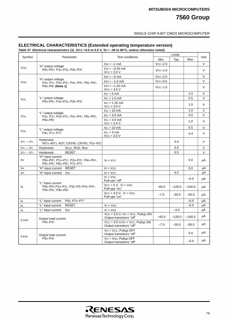
79
SINGLE-CHIP 8-BIT CMOS MICROCOMPUTER
MITSUBISHI MICROCOMPUTERS
7560 Group
VCC = 5.0 V, VO = VCC, Pullup ONOutput transistors “off”
VCC = 3.0 V,VO = VCC, Pullup ONOutput transistors “off”
IOL = 10 mA
IOL = 3.0 mA
IOL = 3.0 mAVCC = 3.0 V
IOL = 5 mA
IOL = 1.5 mA
IOL = 1.25 mAVCC = 3.0 V
VOL
IOH = –1 mA
IOH = –0.25 mAVCC = 3.0 V
IOH = –5 mA
IOH = –1.5 mA
IOH = –1.25 mAVCC = 3.0 V
VVCC–2.0“H” output voltage
P00–P07, P10–P15, P30–P37
Symbol ParameterLimits
Min.Unit
0.5
Typ. Max.Test conditions
VOH
2.0
0.5
ELECTRICAL CHARACTERISTICS (Extended operating temperature version)Table 47 Electrical characteristics (1) (VCC =4.0 to 5.5 V, Ta = –40 to 85°C, unless otherwise noted)
IOL = 10 mA
IOL = 5 mAVCC = 3.0 V
VI = VCC
VI = VCC
VI = VCC
VI = VSSPull-ups “off”
VCC = 5 V, VI = VSSPull-ups “on”
VCC = 3.0 V, VI = VSSPull-ups “on”
VI = VSS
VI = VSS
“H” output voltageP16, P17, P20–P27, P41–P47, P50–P57,P60–P67 (Note 1)
“L” output voltageP00–P07, P10–P15, P30–P37
“L” output voltageP16, P17, P20–P27, P41–P47, P50–P57,P60–P67
“L” output voltageP40, P71–P77
HysteresisINT0–INT2, ADT, CNTR0, CNTR1, P20–P27
Hysteresis SCLK, RXD, SIN2
Hysteresis RESET“H” input current
P00–P07, P10–P17, P20–P27, P40–P47,P50–P57, P60–P67, P70–P77
“H” input current RESET
“H” input current XIN
“L” input currentP00–P07,P10–P17, P20–P27,P41–P47,P50–P57, P60–P67
“L” input current P40, P70–P77
“L” input current RESET
“L” input current XIN
Output load currentP30–P37
VOH
VOL
VOL
VT+ – VT–
VT+ – VT–
VT+ – VT–
IIH
IIH
IIH
IIL
IIL
IIL
ILOAD
VCC–2.0
VCC–0.5
–60.0
–7.0
0.5
0.5
4.0
–120.0
–30.0
–4.0
2.0
0.5
0.5
5.0
5.0
–5.0
–240.0
–55.0
–5.0
–5.0
–240.0
–55.0
V
V
V
V
V
V
V
V
V
V
µAµA
µA
µA
µA
µA
µA
µA
IIL
VCC–1.0
VCC–1.0
V
V
V1.0
V1.0
0.4 V
µA
µA
µA
VO = VCC, Pullup OFFOutput transistors “off”
VO = VSS, Pullup OFFOutput transistors “off”
Output leak currentP30–P37
ILEAK5.0
–5.0 µA
µA
–120.0
–30.0
–60.0
–7.0

80
SINGLE-CHIP 8-BIT CMOS MICROCOMPUTER
7560 GroupMITSUBISHI MICROCOMPUTERS
Table 48 Electrical characteristics (2) (Extended operating temperature version)(VCC =2.5 to 5.5 V, Ta = –20 to 85°C, and VCC =3.0 to 5.5 V, Ta = –40 to –20°C, unless otherwise noted)
V5.5
• High-speed mode, VCC = 5 V
f(XIN) = 8 MHz
f(XCIN) = 32.768 kHz
Output transistors “off”
A-D converter in operating
• High-speed mode, VCC = 5 V
f(XIN) = 8 MHz (in WIT state)
f(XCIN) = 32.768 kHz
Output transistors “off”
A-D converter stop
• Low-speed mode, VCC = 5 V, Ta ≤ 55°C
f(XIN) = stopped
f(XCIN) = 32.768 kHz
Output transistors “off”
• Low-speed mode, VCC = 5 V, Ta = 25°C
f(XIN) = stopped
f(XCIN) = 32.768 kHz (in WIT state)
Output transistors “off”
• Low-speed mode, VCC = 3 V, Ta ≤ 55°C
f(XIN) = stopped
f(XCIN) = 32.768 kHz
Output transistors “off”
• Low-speed mode, VCC = 3 V, Ta = 25°C
f(XIN) = stopped
f(XCIN) = 32.768 kHz (in WIT state)
Output transistors “off”
All oscillation stopped(in STP state)Output transistors “off”
Symbol ParameterLimits
Min.Unit
Typ. Max.Test conditions
ICC Power source current
6.4
VRAM RAM retention voltage At clock stop mode 2.0
When using voltage multiplier
VL1 = 1.8 V
VL1
IL1
Power source voltage
Power source current(VL1) (Note)
Note: When the voltage multiplier control bit of the LCD mode register (bit 4 at address 003916) is “1”.
1.3
1.3
1.6
35
20
15
4.5
0.1
1.8
1.8
4.0
3.2
70
40
22
9.0
1.0
10
2.1
2.3
mA
µA
µA
µA
µA
µA
V
mA13
µA
Ta = 25 °C
Ta = 85 °C
M37560MFD
M37560EFD
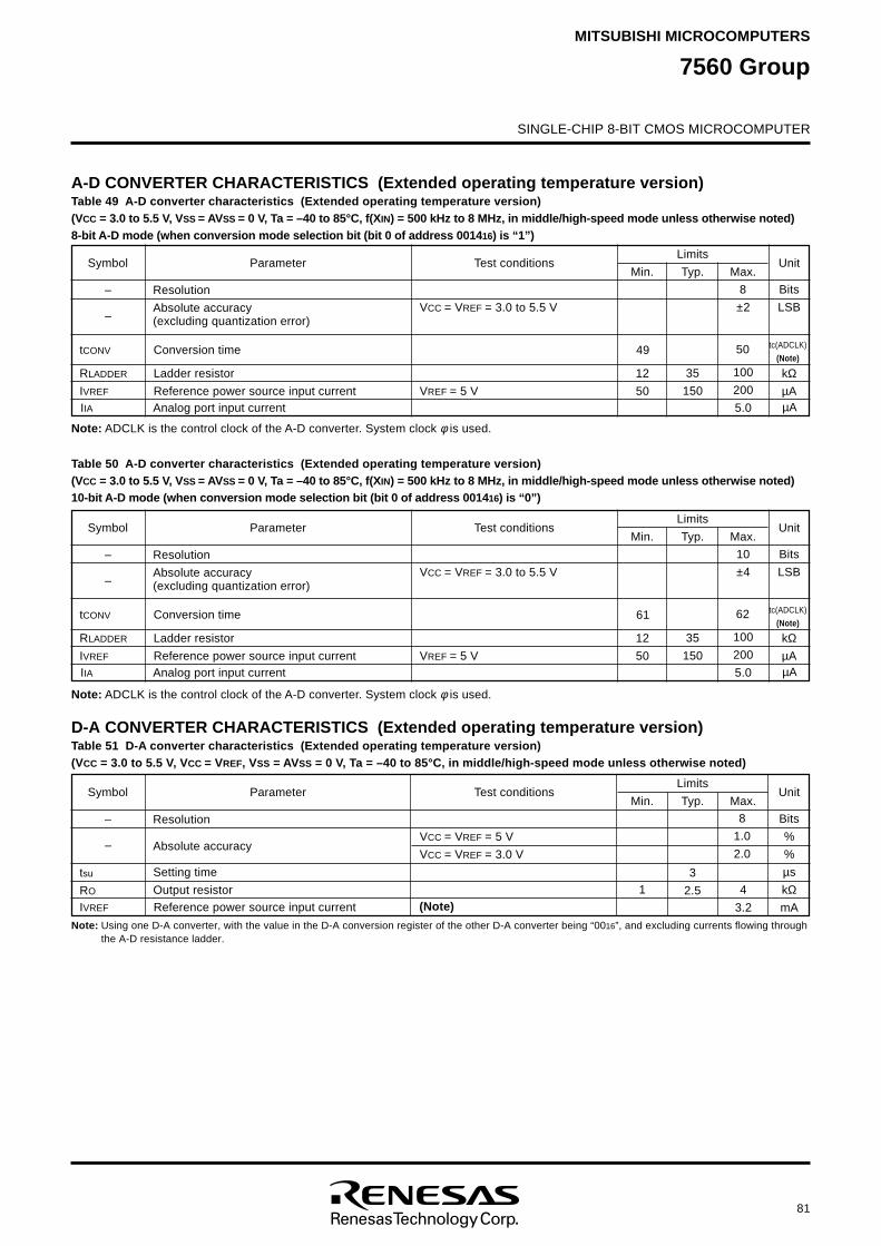
81
SINGLE-CHIP 8-BIT CMOS MICROCOMPUTER
MITSUBISHI MICROCOMPUTERS
7560 Group
A-D CONVERTER CHARACTERISTICS (Extended operating temperature version)Table 49 A-D converter characteristics (Extended operating temperature version)(VCC = 3.0 to 5.5 V, VSS = AVSS = 0 V, Ta = –40 to 85°C, f(XIN) = 500 kHz to 8 MHz, in middle/high-speed mode unless otherwise noted)8-bit A-D mode (when conversion mode selection bit (bit 0 of address 001416) is “1”)
Symbol ParameterLimits
Min.Unit
Typ. Max.Test conditions
– Resolution
Absolute accuracy(excluding quantization error)
VCC = VREF = 3.0 to 5.5 V
Bits
LSB
35
150
8
±2
tc(ADCLK)
(Note)Conversion time
Ladder resistor
Reference power source input current
–
tCONV
RLADDER
IVREF
kΩµA
D-A CONVERTER CHARACTERISTICS (Extended operating temperature version)Table 51 D-A converter characteristics (Extended operating temperature version)(VCC = 3.0 to 5.5 V, VCC = VREF, VSS = AVSS = 0 V, Ta = –40 to 85°C, in middle/high-speed mode unless otherwise noted)
Symbol ParameterLimits
Min.Unit
Typ. Max.Test conditions
– Resolution
VCC = VREF = 5 V
VCC = VREF = 3.0 V
1
Bits
%
%
µs
kΩmA
3
2.5
8
1.0
2.0
Note: Using one D-A converter, with the value in the D-A conversion register of the other D-A converter being “0016”, and excluding currents flowing throughthe A-D resistance ladder.
(Note)
Setting time
Output resistor
–
tsu
RO 4
3.2
12
50
Absolute accuracy
Analog port input currentIIA
IVREF Reference power source input current
µA
100
200
5.0VREF = 5 V
Table 50 A-D converter characteristics (Extended operating temperature version)(VCC = 3.0 to 5.5 V, VSS = AVSS = 0 V, Ta = –40 to 85°C, f(XIN) = 500 kHz to 8 MHz, in middle/high-speed mode unless otherwise noted)10-bit A-D mode (when conversion mode selection bit (bit 0 of address 001416) is “0”)
49 50
Symbol ParameterLimits
Min.Unit
Typ. Max.Test conditions
– Resolution
Absolute accuracy(excluding quantization error)
VCC = VREF = 3.0 to 5.5 V
Bits
LSB
35
150
10
±4
tc(ADCLK)
(Note)Conversion time
Ladder resistor
Reference power source input current
–
tCONV
RLADDER
IVREF
kΩµA
12
50Analog port input currentIIA µA
100
200
5.0VREF = 5 V
61 62
Note: ADCLK is the control clock of the A-D converter. System clock φ is used.
Note: ADCLK is the control clock of the A-D converter. System clock φ is used.
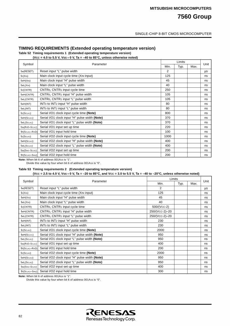
82
SINGLE-CHIP 8-BIT CMOS MICROCOMPUTER
7560 GroupMITSUBISHI MICROCOMPUTERS
TIMING REQUIREMENTS (Extended operating temperature version)Table 52 Timing requirements 1 (Extended operating temperature version)
(VCC = 4.0 to 5.5 V, VSS = 0 V, Ta = –40 to 85°C, unless otherwise noted)
2
125
45
40
250
105
105
80
80
800
370
370
220
100
1000
400
400
200
200
Note: When bit 6 of address 001A16 is “1”.Divide this value by four when bit 6 of address 001A16 is “0”.
Reset input “L” pulse width
Main clock input cycle time (XIN input)
Main clock input “H” pulse width
Main clock input “L” pulse width
CNTR0, CNTR1 input cycle time
CNTR0, CNTR1 input “H” pulse width
CNTR0, CNTR1 input “L” pulse width
INT0 to INT2 input “H” pulse width
INT0 to INT2 input “L” pulse width
Serial I/O1 clock input cycle time (Note)
Serial I/O1 clock input “H” pulse width (Note)
Serial I/O1 clock input “L” pulse width (Note)
Serial I/O1 input set up time
Serial I/O1 input hold time
Serial I/O2 clock input cycle time (Note)
Serial I/O2 clock input “H” pulse width (Note)
Serial I/O2 clock input “L” pulse width (Note)
Serial I/O2 input set up time
Serial I/O2 input hold time
tw(RESET)
tc(XIN)
twH(XIN)
twL(XIN)
tc(CNTR)
twH(CNTR)
twL(CNTR)
twH(INT)
twL(INT)
tc(SCLK1)
twH(SCLK1)
twL(SCLK1)
tsu(RXD–SCLK1)
th(SCLK1–RXD)
tc(SCLK2)
twH(SCLK2)
twL(SCLK2)
tsu(SIN2–SCLK2)
th(SCLK2–SIN2)
Symbol ParameterLimits
Min.
µs
ns
ns
ns
ns
ns
ns
ns
ns
ns
ns
ns
ns
ns
ns
ns
ns
ns
ns
UnitTyp. Max.
Table 53 Timing requirements 2 (Extended operating temperature version)(VCC = 2.5 to 4.0 V, VSS = 0 V, Ta = –20 to 85°C, and VCC = 3.0 to 5.5 V, Ta = –40 to –20°C, unless otherwise noted)
2
125
45
40
500/(VCC-2)
250/(VCC-2)–20
250/(VCC-2)–20
230
230
2000
950
Reset input “L” pulse width
Main clock input cycle time (XIN input)
Main clock input “H” pulse width
Main clock input “L” pulse width
CNTR0, CNTR1 input cycle time
CNTR0, CNTR1 input “H” pulse width
CNTR0, CNTR1 input “L” pulse width
INT0 to INT2 input “H” pulse width
INT0 to INT2 input “L” pulse width
Serial I/O1 clock input cycle time (Note)
Serial I/O1 clock input “H” pulse width (Note)
tw(RESET)
tc(XIN)
twH(XIN)
twL(XIN)
tc(CNTR)
twH(CNTR)
twL(CNTR)
twH(INT)
twL(INT)
tc(SCLK1)
twH(SCLK1)
Symbol ParameterLimits
Min.
µs
ns
ns
ns
ns
ns
ns
ns
ns
ns
ns
UnitTyp. Max.
Note: When bit 6 of address 001A16 is “1”.Divide this value by four when bit 6 of address 001A16 is “0”.
tsu(SIN2–SCLK2)
th(SCLK2–SIN2)
twL(SCLK1)
tsu(RXD–SCLK1)
th(SCLK1–RXD)
tc(SCLK2)
twH(SCLK2)
twL(SCLK2)
Serial I/O1 clock input “L” pulse width (Note)
Serial I/O1 input set up time
Serial I/O1 input hold time
Serial I/O2 clock input cycle time (Note)
Serial I/O2 clock input “H” pulse width (Note)
Serial I/O2 clock input “L” pulse width (Note)Serial I/O2 input set up time
Serial I/O2 input hold time
950
400
200
2000
950
950400
300
ns
ns
ns
ns
ns
nsns
ns
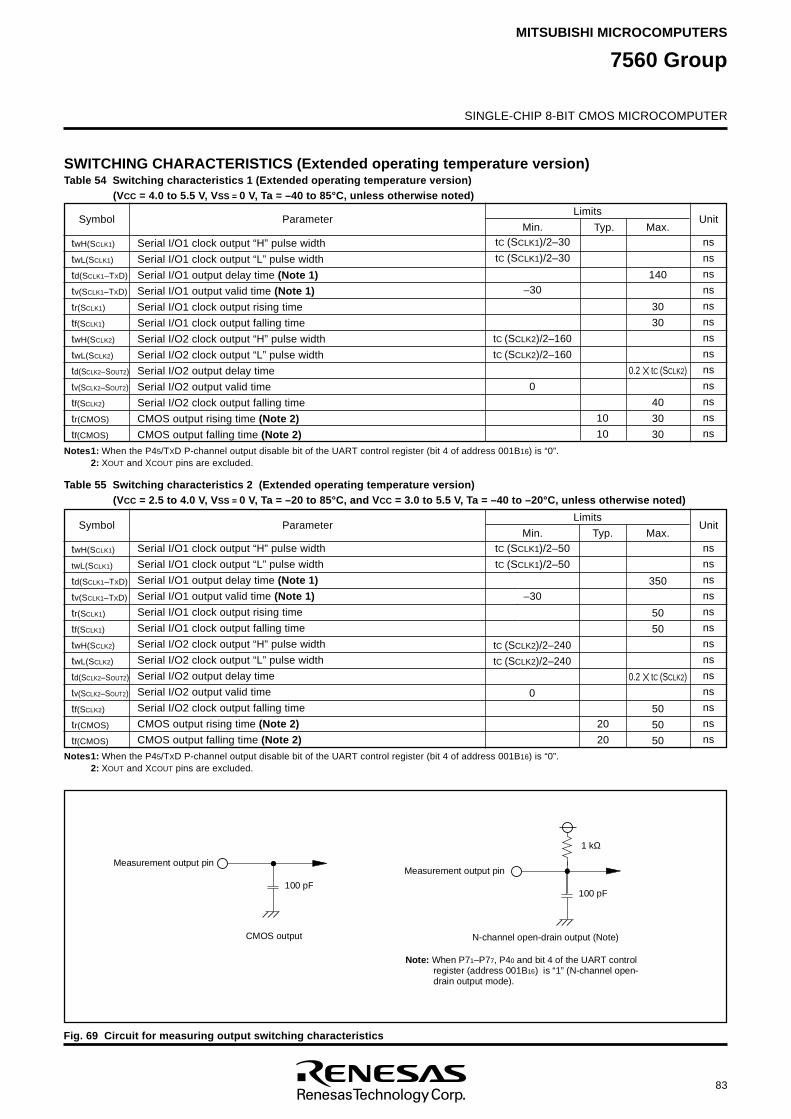
83
SINGLE-CHIP 8-BIT CMOS MICROCOMPUTER
MITSUBISHI MICROCOMPUTERS
7560 Group
SWITCHING CHARACTERISTICS (Extended operating temperature version)Table 54 Switching characteristics 1 (Extended operating temperature version)
(VCC = 4.0 to 5.5 V, VSS = 0 V, Ta = –40 to 85°C, unless otherwise noted)
Notes1: When the P45/TXD P-channel output disable bit of the UART control register (bit 4 of address 001B16) is “0”.2: XOUT and XCOUT pins are excluded.
Serial I/O1 clock output “H” pulse width
Serial I/O1 clock output “L” pulse width
Serial I/O1 output delay time (Note 1)
Serial I/O1 output valid time (Note 1)
Serial I/O1 clock output rising time
Serial I/O1 clock output falling time
Serial I/O2 clock output “H” pulse width
Serial I/O2 clock output “L” pulse width
Serial I/O2 output delay time
Serial I/O2 output valid time
Serial I/O2 clock output falling time
CMOS output rising time (Note 2)
CMOS output falling time (Note 2)
140
30
30
0.2 tC (SCLK2)
40
30
30
Symbol ParameterLimits
Min.ns
ns
ns
ns
ns
ns
ns
ns
ns
ns
ns
ns
ns
Unit
tC (SCLK1)/2–30
tC (SCLK1)/2–30
–30
10
10
Typ. Max.
twH(SCLK1)
twL(SCLK1)
td(SCLK1–TXD)
tv(SCLK1–TXD)
tr(SCLK1)
tf(SCLK1)
twH(SCLK2)
twL(SCLK2)
td(SCLK2–SOUT2)
tv(SCLK2–SOUT2)
tf(SCLK2)
tr(CMOS)
tf(CMOS)
Table 55 Switching characteristics 2 (Extended operating temperature version)(VCC = 2.5 to 4.0 V, VSS = 0 V, Ta = –20 to 85°C, and VCC = 3.0 to 5.5 V, Ta = –40 to –20°C, unless otherwise noted)
ns
ns
ns
ns
ns
ns
ns
ns
ns
ns
ns
ns
ns
Unit
Notes1: When the P45/TXD P-channel output disable bit of the UART control register (bit 4 of address 001B16) is “0”.2: XOUT and XCOUT pins are excluded.
Serial I/O1 clock output “H” pulse width
Serial I/O1 clock output “L” pulse width
Serial I/O1 output delay time (Note 1)
Serial I/O1 output valid time (Note 1)
Serial I/O1 clock output rising time
Serial I/O1 clock output falling time
Serial I/O2 clock output “H” pulse width
Serial I/O2 clock output “L” pulse width
Serial I/O2 output delay time
Serial I/O2 output valid time
Serial I/O2 clock output falling time
CMOS output rising time (Note 2)
CMOS output falling time (Note 2)
350
50
50
0.2 tC (SCLK2)
50
50
50
Symbol ParameterLimits
Min.tC (SCLK1)/2–50
tC (SCLK1)/2–50
–30
20
20
Max.
twH(SCLK1)
twL(SCLK1)
td(SCLK1–TXD)
tv(SCLK1–TXD)
tr(SCLK1)
tf(SCLK1)
twH(SCLK2)
twL(SCLK2)
td(SCLK2–SOUT2)
tv(SCLK2–SOUT2)
tf(SCLK2)
tr(CMOS)
tf(CMOS)
Typ.
tC (SCLK2)/2–160
tC (SCLK2)/2–160
0
tC (SCLK2)/2–240
tC (SCLK2)/2–240
0
Fig. 69 Circuit for measuring output switching characteristics
Measurement output pin
1
0
0
p
F
C
M
O
S
o
u
t
p
u
t
N
o
t
e
:
W
h
e
n
P
71–
P
77,
P
40
a
n
d
b
i
t
4
o
f
t
h
e
U
A
R
T
c
o
n
t
r
o
l
r
e
g
i
s
t
e
r
(
a
d
d
r
e
s
s
0
0
1
B1
6)
i
s
“
1
”
(
N
-
c
h
a
n
n
e
l
o
p
e
n
-d
r
a
i
n
o
u
t
p
u
t
m
o
d
e
)
.
N
-
c
h
a
n
n
e
l
o
p
e
n
-
d
r
a
i
n
o
u
t
p
u
t
(
N
o
t
e
)
1 kΩ
1
0
0
p
F
Measurement output pin
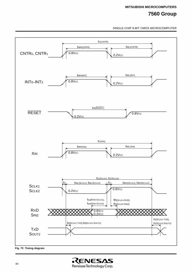
84
SINGLE-CHIP 8-BIT CMOS MICROCOMPUTER
7560 GroupMITSUBISHI MICROCOMPUTERS
Fig. 70 Timing diagram
I N
T0
–I
N
T2
C
N
T
R0,
C
N
T
R1
0.2VCC
tW
L
(
I
N
T
)
0.8VCC
tWH(INT)
0.2VCC
0.2VCC0.8VCC
0.8VCC
0.2VCC
tW
L
(
XI
N)
0.8VCC
tWH(XIN)
tC(XIN)
XI
N
0.2VCC0 .
8
VC
C
tW(RESET)
RESET
tf tr
0 .
2
VC
C
tWL(CNTR)
0 .
8
VC
C
tWH(CNTR)
tC(CNTR)
td
(
SC
L
K
1-
TXD
),
td
(
SC
L
K
2
-SO
U
T
2)
tv(SCLK1-TXD),
tv(SCLK2-SOUT2)
tC(SCLK1), tC(SCLK2)
tWL(SCLK1), tWL(SCLK2) tWH(SCLK1), tWH(SCLK2)
th(SCLK1-RXD),
th(SCLK2-SIN2)
tsu(RXD-SCLK1),
tsu(SIN2-SCLK2)
TXDSOUT2
RXDSIN2
SCLK1
SCLK2
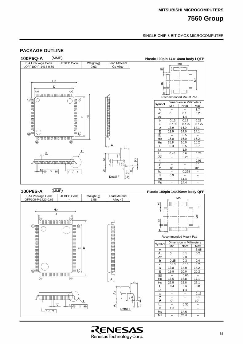
85
SINGLE-CHIP 8-BIT CMOS MICROCOMPUTER
MITSUBISHI MICROCOMPUTERS
7560 Group
PACKAGE OUTLINE
LQFP100-P-1414-0.50Weight(g)
– 0.63JEDEC CodeEIAJ Package Code Lead Material
Cu Alloy
100P6Q-A Plastic 100pin 14 14mm body LQFP
–0.1
–
– –0.2
––
– –
––
––
–
SymbolMin Nom Max
A
A2
bcDE
HE
LL1
y
b2
Dimension in Millimeters
HD
A1
0.225––I2 0.9––MD 14.4––ME 14.4
10°0°0.1
1.00.70.50.3
16.216.015.816.216.015.8
0.514.114.013.914.114.013.90.1750.1250.1050.280.180.13
1.40
1.7
e
e
E HE
1
76
75
51
5026
25
HD
D
A
F
y
100
Lp 0.45––
0.60.25–
0.75–
0.08xA3
b x M A1
A2
L1
L
Detail F Lp
A3
c
MD
l2
b2
ME
e
Recommended Mount Pad
MMP
QFP100-P-1420-0.65 1.58Weight(g)
–JEDEC CodeEIAJ Package Code Lead Material
Alloy 42
100P6S-A Plastic 100pin 14 20mm body QFP
–0.1
–
– –0.2
––
– –
––
––
–
SymbolMin Nom Max
A
A2
bcDE
HE
LL1
y
b2
Dimension in Millimeters
HD
A1
0.35––I2 1.3––MD 14.6––ME 20.6
10°0°0.1
1.40.80.60.4
23.122.822.517.116.816.5
0.6520.220.019.814.214.013.8
0.20.150.130.40.30.25
2.80
3.05
e
e
e
E
c
HE
1
30
31
81
50
80
51
HD
D
MDM
E
A
F
A1
A2
L1
L
y
b2
I2
Recommended Mount Pad
Detail F
100
x – – 0.13
b x M
MMP
© 2003 MITSUBISHI ELECTRIC CORP.Specifications subject to change without notice.
Notes regarding these materials• These materials are intended as a reference to assist our customers in the selection of the Mitsubishi semiconductor product best suited to the customer’s application; they do not convey any license under any intellectual property
rights, or any other rights, belonging to Mitsubishi Electric Corporation or a third party.• Mitsubishi Electric Corporation assumes no responsibility for any damage, or infringement of any third-party’s rights, originating in the use of any product data, diagrams, charts, programs, algorithms, or circuit application examples
contained in these materials.• All information contained in these materials, including product data, diagrams, charts, programs and algorithms represents information on products at the time of publication of these materials, and are subject to change by
Mitsubishi Electric Corporation without notice due to product improvements or other reasons. It is therefore recommended that customers contact Mitsubishi Electric Corporation or an authorized Mitsubishi Semiconductor productdistributor for the latest product information before purchasing a product listed herein.The information described here may contain technical inaccuracies or typographical errors. Mitsubishi Electric Corporation assumes no responsibility for any damage, liability, or other loss rising from these inaccuracies or errors.Please also pay attention to information published by Mitsubishi Electric Corporation by various means, including the Mitsubishi Semiconductor home page (http://www.mitsubishichips.com).
• When using any or all of the information contained in these materials, including product data, diagrams, charts, programs, and algorithms, please be sure to evaluate all information as a total system before making a final decisionon the applicability of the information and products. Mitsubishi Electric Corporation assumes no responsibility for any damage, liability or other loss resulting from the information contained herein.
• Mitsubishi Electric Corporation semiconductors are not designed or manufactured for use in a device or system that is used under circumstances in which human life is potentially at stake. Please contact Mitsubishi ElectricCorporation or an authorized Mitsubishi Semiconductor product distributor when considering the use of a product contained herein for any specific purposes, such as apparatus or systems for transportation, vehicular, medical,aerospace, nuclear, or undersea repeater use.
• The prior written approval of Mitsubishi Electric Corporation is necessary to reprint or reproduce in whole or in part these materials.• If these products or technologies are subject to the Japanese export control restrictions, they must be exported under a license from the Japanese government and cannot be imported into a country other than the approved
destination.Any diversion or reexport contrary to the export control laws and regulations of Japan and/or the country of destination is prohibited.
• Please contact Mitsubishi Electric Corporation or an authorized Mitsubishi Semiconductor product distributor for further details on these materials or the products contained therein.
Keep safety first in your circuit designs!• Mitsubishi Electric Corporation puts the maximum effort into making semiconductor products better and more reliable, but there is always the possibility that trouble may occur with them. Trouble with semiconductors may lead to
personal injury, fire or property damage. Remember to give due consideration to safety when making your circuit designs, with appropriate measures such as (i) placement of substitutive, auxiliary circuits, (ii) use of non-flammablematerial or (iii) prevention against any malfunction or mishap.
SINGLE-CHIP 8-BIT CMOS MICROCOMPUTER
7560 GroupMITSUBISHI MICROCOMPUTERS
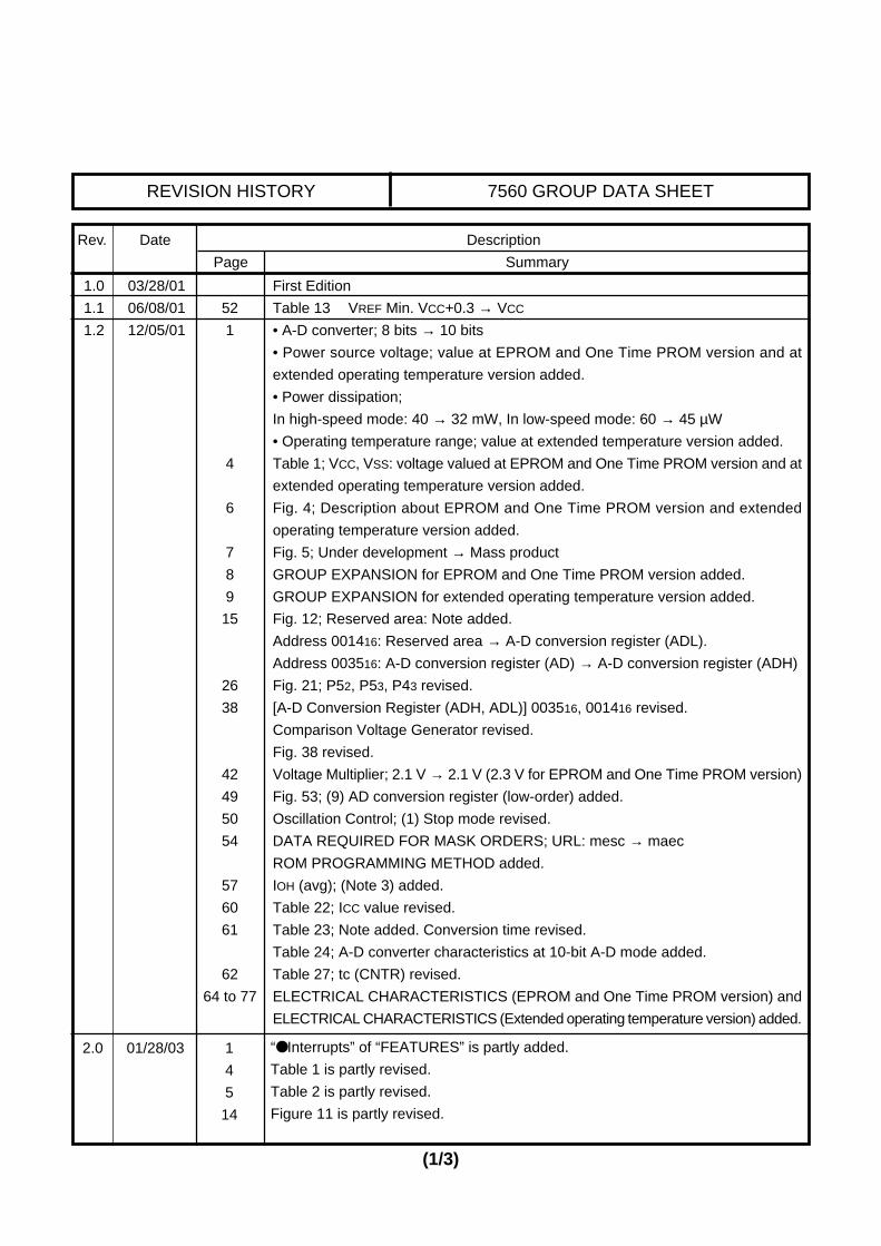
REVISION HISTORY 7560 GROUP DATA SHEET
Rev. Date Description
Page Summary
(1/3)
1.0 03/28/01
1.1 06/08/01
1.2 12/05/01
First Edition
Table 13 VREF Min. VCC+0.3 → VCC
• A-D converter; 8 bits → 10 bits
• Power source voltage; value at EPROM and One Time PROM version and at
extended operating temperature version added.
• Power dissipation;
In high-speed mode: 40 → 32 mW, In low-speed mode: 60 → 45 µW
• Operating temperature range; value at extended temperature version added.
Table 1; VCC, VSS: voltage valued at EPROM and One Time PROM version and at
extended operating temperature version added.
Fig. 4; Description about EPROM and One Time PROM version and extended
operating temperature version added.
Fig. 5; Under development → Mass product
GROUP EXPANSION for EPROM and One Time PROM version added.
GROUP EXPANSION for extended operating temperature version added.
Fig. 12; Reserved area: Note added.
Address 001416: Reserved area → A-D conversion register (ADL).
Address 003516: A-D conversion register (AD) → A-D conversion register (ADH)
Fig. 21; P52, P53, P43 revised.
[A-D Conversion Register (ADH, ADL)] 003516, 001416 revised.
Comparison Voltage Generator revised.
Fig. 38 revised.
Voltage Multiplier; 2.1 V → 2.1 V (2.3 V for EPROM and One Time PROM version)
Fig. 53; (9) AD conversion register (low-order) added.
Oscillation Control; (1) Stop mode revised.
DATA REQUIRED FOR MASK ORDERS; URL: mesc → maec
ROM PROGRAMMING METHOD added.
IOH (avg); (Note 3) added.
Table 22; ICC value revised.
Table 23; Note added. Conversion time revised.
Table 24; A-D converter characteristics at 10-bit A-D mode added.
Table 27; tc (CNTR) revised.
ELECTRICAL CHARACTERISTICS (EPROM and One Time PROM version) and
ELECTRICAL CHARACTERISTICS (Extended operating temperature version) added.
52
1
4
6
7
8
9
15
26
38
42
49
50
54
57
60
61
62
64 to 77
2.0 01/28/03 1
4
5
14
“ Interrupts” of “FEATURES” is partly added.
Table 1 is partly revised.
Table 2 is partly revised.
Figure 11 is partly revised.
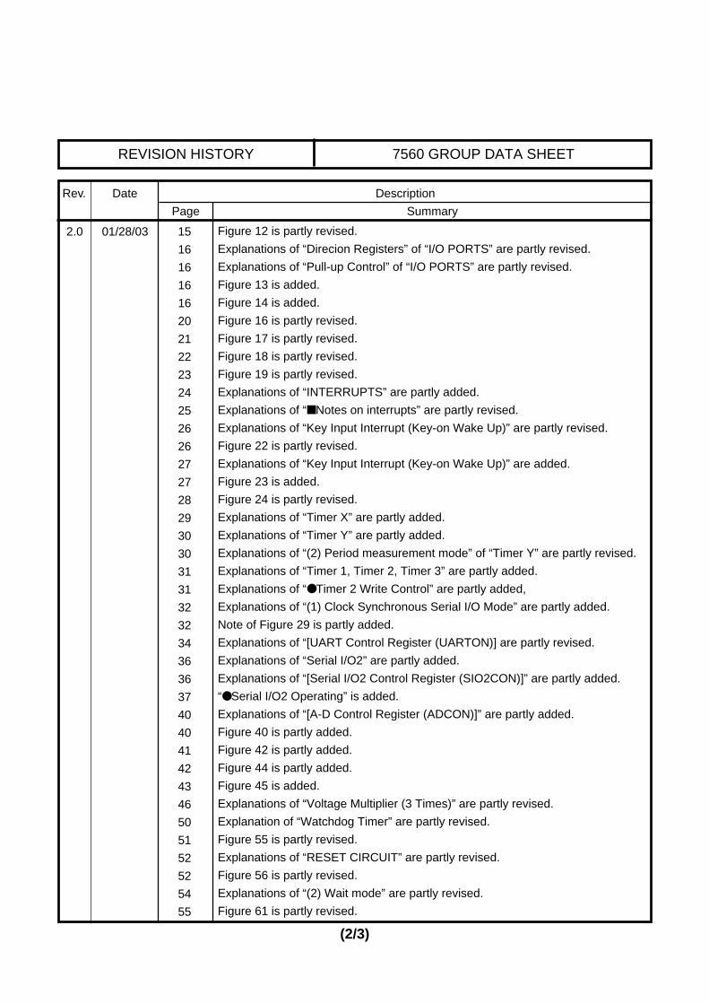
REVISION HISTORY 7560 GROUP DATA SHEET
Rev. Date Description
Page Summary
(2/3)
2.0 01/28/03 15
16
16
16
16
20
21
22
23
24
25
26
26
27
27
28
29
30
30
31
31
32
32
34
36
36
37
40
40
41
42
43
46
50
51
52
52
54
55
Figure 12 is partly revised.
Explanations of “Direcion Registers” of “I/O PORTS” are partly revised.
Explanations of “Pull-up Control” of “I/O PORTS” are partly revised.
Figure 13 is added.
Figure 14 is added.
Figure 16 is partly revised.
Figure 17 is partly revised.
Figure 18 is partly revised.
Figure 19 is partly revised.
Explanations of “INTERRUPTS” are partly added.
Explanations of “ Notes on interrupts” are partly revised.
Explanations of “Key Input Interrupt (Key-on Wake Up)” are partly revised.
Figure 22 is partly revised.
Explanations of “Key Input Interrupt (Key-on Wake Up)” are added.
Figure 23 is added.
Figure 24 is partly revised.
Explanations of “Timer X” are partly added.
Explanations of “Timer Y” are partly added.
Explanations of “(2) Period measurement mode” of “Timer Y” are partly revised.
Explanations of “Timer 1, Timer 2, Timer 3” are partly added.
Explanations of “ Timer 2 Write Control” are partly added,
Explanations of “(1) Clock Synchronous Serial I/O Mode” are partly added.
Note of Figure 29 is partly added.
Explanations of “[UART Control Register (UARTON)] are partly revised.
Explanations of “Serial I/O2” are partly added.
Explanations of “[Serial I/O2 Control Register (SIO2CON)]” are partly added.
“ Serial I/O2 Operating” is added.
Explanations of “[A-D Control Register (ADCON)]” are partly added.
Figure 40 is partly added.
Figure 42 is partly added.
Figure 44 is partly added.
Figure 45 is added.
Explanations of “Voltage Multiplier (3 Times)” are partly revised.
Explanation of “Watchdog Timer” are partly revised.
Figure 55 is partly revised.
Explanations of “RESET CIRCUIT” are partly revised.
Figure 56 is partly revised.
Explanations of “(2) Wait mode” are partly revised.
Figure 61 is partly revised.
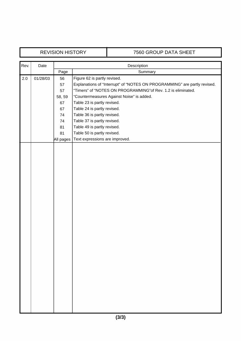
REVISION HISTORY 7560 GROUP DATA SHEET
Rev. Date Description
Page Summary
(3/3)
2.0 01/28/03 56
57
57
58, 59
67
67
74
74
81
81
All pages
Figure 62 is partly revised.
Explanations of “Interrupt” of “NOTES ON PROGRAMMING” are partly revised.
“Timers” of “NOTES ON PROGRAMMING”of Rev. 1.2 is eliminated.
“Countermeasures Against Noise” is added.
Table 23 is partly revised.
Table 24 is partly revised.
Table 36 is partly revised.
Table 37 is partly revised.
Table 49 is partly revised.
Table 50 is partly revised.
Text expressions are improved.