Embed Size (px)
Citation preview
To our customers,
Old Company Name in Catalogs and Other Documents
On April 1st, 2010, NEC Electronics Corporation merged with Renesas Technology
Corporation, and Renesas Electronics Corporation took over all the business of both companies. Therefore, although the old company name remains in this document, it is a valid Renesas Electronics document. We appreciate your understanding.
Renesas Electronics website: http://www.renesas.com
April 1st, 2010 Renesas Electronics Corporation
Issued by: Renesas Electronics Corporation (http://www.renesas.com)
Send any inquiries to http://www.renesas.com/inquiry.
Notice 1. All information included in this document is current as of the date this document is issued. Such information, however, is
subject to change without any prior notice. Before purchasing or using any Renesas Electronics products listed herein, please confirm the latest product information with a Renesas Electronics sales office. Also, please pay regular and careful attention to additional and different information to be disclosed by Renesas Electronics such as that disclosed through our website.
2. Renesas Electronics does not assume any liability for infringement of patents, copyrights, or other intellectual property rights of third parties by or arising from the use of Renesas Electronics products or technical information described in this document. No license, express, implied or otherwise, is granted hereby under any patents, copyrights or other intellectual property rights of Renesas Electronics or others.
3. You should not alter, modify, copy, or otherwise misappropriate any Renesas Electronics product, whether in whole or in part. 4. Descriptions of circuits, software and other related information in this document are provided only to illustrate the operation of
semiconductor products and application examples. You are fully responsible for the incorporation of these circuits, software, and information in the design of your equipment. Renesas Electronics assumes no responsibility for any losses incurred by you or third parties arising from the use of these circuits, software, or information.
5. When exporting the products or technology described in this document, you should comply with the applicable export control laws and regulations and follow the procedures required by such laws and regulations. You should not use Renesas Electronics products or the technology described in this document for any purpose relating to military applications or use by the military, including but not limited to the development of weapons of mass destruction. Renesas Electronics products and technology may not be used for or incorporated into any products or systems whose manufacture, use, or sale is prohibited under any applicable domestic or foreign laws or regulations.
6. Renesas Electronics has used reasonable care in preparing the information included in this document, but Renesas Electronics does not warrant that such information is error free. Renesas Electronics assumes no liability whatsoever for any damages incurred by you resulting from errors in or omissions from the information included herein.
7. Renesas Electronics products are classified according to the following three quality grades: “Standard”, “High Quality”, and “Specific”. The recommended applications for each Renesas Electronics product depends on the product’s quality grade, as indicated below. You must check the quality grade of each Renesas Electronics product before using it in a particular application. You may not use any Renesas Electronics product for any application categorized as “Specific” without the prior written consent of Renesas Electronics. Further, you may not use any Renesas Electronics product for any application for which it is not intended without the prior written consent of Renesas Electronics. Renesas Electronics shall not be in any way liable for any damages or losses incurred by you or third parties arising from the use of any Renesas Electronics product for an application categorized as “Specific” or for which the product is not intended where you have failed to obtain the prior written consent of Renesas Electronics. The quality grade of each Renesas Electronics product is “Standard” unless otherwise expressly specified in a Renesas Electronics data sheets or data books, etc.
“Standard”: Computers; office equipment; communications equipment; test and measurement equipment; audio and visual equipment; home electronic appliances; machine tools; personal electronic equipment; and industrial robots.
“High Quality”: Transportation equipment (automobiles, trains, ships, etc.); traffic control systems; anti-disaster systems; anti-crime systems; safety equipment; and medical equipment not specifically designed for life support.
“Specific”: Aircraft; aerospace equipment; submersible repeaters; nuclear reactor control systems; medical equipment or systems for life support (e.g. artificial life support devices or systems), surgical implantations, or healthcare intervention (e.g. excision, etc.), and any other applications or purposes that pose a direct threat to human life.
8. You should use the Renesas Electronics products described in this document within the range specified by Renesas Electronics, especially with respect to the maximum rating, operating supply voltage range, movement power voltage range, heat radiation characteristics, installation and other product characteristics. Renesas Electronics shall have no liability for malfunctions or damages arising out of the use of Renesas Electronics products beyond such specified ranges.
9. Although Renesas Electronics endeavors to improve the quality and reliability of its products, semiconductor products have specific characteristics such as the occurrence of failure at a certain rate and malfunctions under certain use conditions. Further, Renesas Electronics products are not subject to radiation resistance design. Please be sure to implement safety measures to guard them against the possibility of physical injury, and injury or damage caused by fire in the event of the failure of a Renesas Electronics product, such as safety design for hardware and software including but not limited to redundancy, fire control and malfunction prevention, appropriate treatment for aging degradation or any other appropriate measures. Because the evaluation of microcomputer software alone is very difficult, please evaluate the safety of the final products or system manufactured by you.
10. Please contact a Renesas Electronics sales office for details as to environmental matters such as the environmental compatibility of each Renesas Electronics product. Please use Renesas Electronics products in compliance with all applicable laws and regulations that regulate the inclusion or use of controlled substances, including without limitation, the EU RoHS Directive. Renesas Electronics assumes no liability for damages or losses occurring as a result of your noncompliance with applicable laws and regulations.
11. This document may not be reproduced or duplicated, in any form, in whole or in part, without prior written consent of Renesas Electronics.
12. Please contact a Renesas Electronics sales office if you have any questions regarding the information contained in this document or Renesas Electronics products, or if you have any other inquiries.
(Note 1) “Renesas Electronics” as used in this document means Renesas Electronics Corporation and also includes its majority-owned subsidiaries.
(Note 2) “Renesas Electronics product(s)” means any product developed or manufactured by or for Renesas Electronics.
6©
CONTENTS
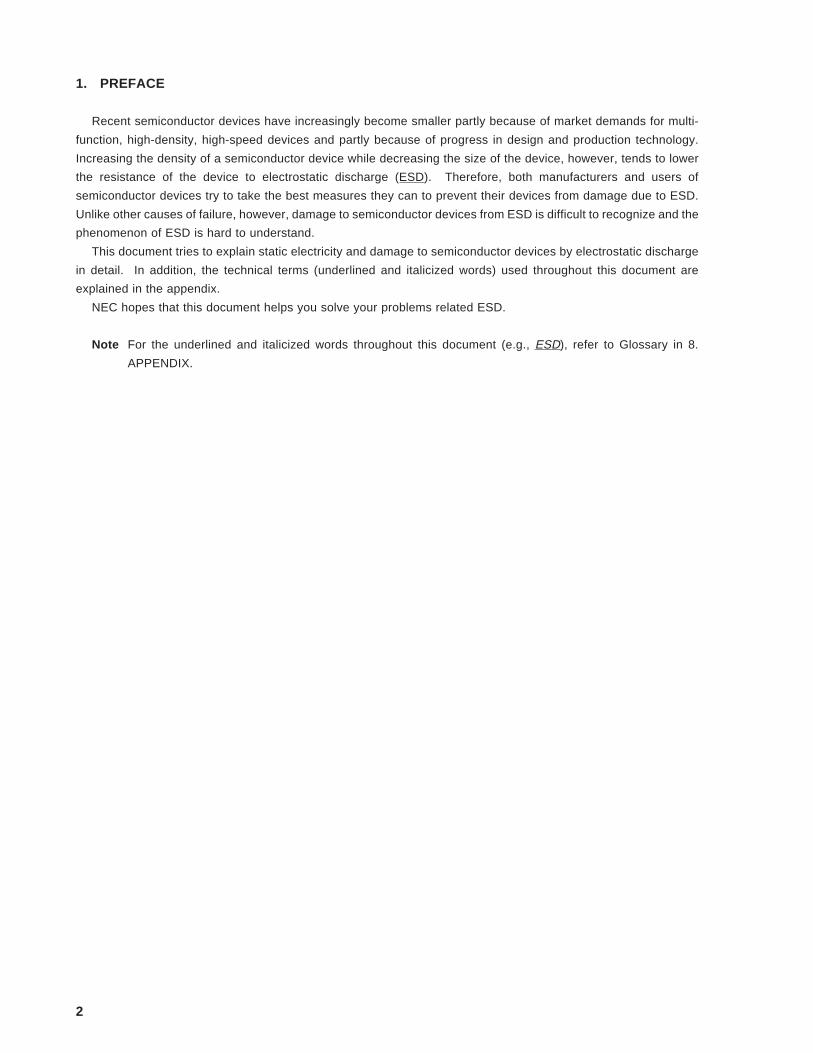
1. PREFACE ....................................................................................................................................... 2
2. ESD AND EOS ............................................................................................................................... 3
3. GENERATION OF STATIC ELECTRICITY .................................................................................... 4
4. DAMAGE TO SEMICONDUCTOR DEVICES BY ESD ................................................................. 54.1 Why Are Semiconductor Devices Damaged by Electrostatic Discharge ? ..................... 54.2 Resistance of Each Type of Semiconductor Device to Electrostatic Discharg e ........... 54.3 Major Modes of Damages by ES D ...................................................................................... 64.4 Protection Circuits of Semiconductor Device s ................................................................. 8
5. MODELS OF DAMAGE BY ES D ................................................................................................... 9
6. ELECTROSTATIC DISCHARGE TESTS ....................................................................................... 106.1 Outline of Electrostatic Discharge Tests ........................................................................... 106.2 Reviewing Standards of Electrostatic Discharge Tests ................................................... 126.3 Application of Electrostatic Discharge Tests .................................................................... 126.4 NEC’s Electrostatic Discharge Tests ................................................................................. 13
7. GENERAL POINTS TO BE NOTED ON ESD ............................................................................... 137.1 When Packaging Semiconductor Device s ........................................................................ 147.2 Working Environment s ........................................................................................................ 157.3 Equipment, Jigs, and Tool s ................................................................................................. 167.4 Notes on Workin g ................................................................................................................ 17
8. APPENDIX ...................................................................................................................................... 198.1 Glossar y ................................................................................................................................ 198.2 Manufacturers of Products to Prevent Damages by ES D ................................................ 20
GUIDE TO PREVENT DAMAGE FOR SEMICONDUCTOR DEVICESBY ELECTROSTATIC DISCHARGE (ESD)
Document No. C11892EJ1V1IF00 (1st edition)Date Published July 1997 NPrinted in Japan
1997
2
1. PREFACE
Recent semiconductor devices have increasingly become smaller partly because of market demands for multi-
function, high-density, high-speed devices and partly because of progress in design and production technology.
Increasing the density of a semiconductor device while decreasing the size of the device, however, tends to lower
the resistance of the device to electrostatic discharge (ESD). Therefore, both manufacturers and users of
semiconductor devices try to take the best measures they can to prevent their devices from damage due to ESD.
Unlike other causes of failure, however, damage to semiconductor devices from ESD is difficult to recognize and the
phenomenon of ESD is hard to understand.
This document tries to explain static electricity and damage to semiconductor devices by electrostatic discharge
in detail. In addition, the technical terms (underlined and italicized words) used throughout this document are
explained in the appendix.
NEC hopes that this document helps you solve your problems related ESD.
Note For the underlined and italicized words throughout this document (e.g., ESD), refer to Glossary in 8.
APPENDIX.
3
2. ESD AND EOS
Both ESD (electrostatic discharge) and EOS (electrical over stress) are phenomena that cause damage to
semiconductor devices. The major difference between these is the process by which a given semiconductor device
is damaged. However, it is often difficult to identify and distinguish between these two phenomena because it is difficult
to find which of the two is responsible for the damage done to the device. This section therefore explains briefly the
differences between ESD and EOS.
Table 1-1. Differences between ESD and EOS
Symptoms of Damage by EOS
If the energy of EOS is large, the areas of damage,
such as breaks in wiring on the chip due to melting,
discoloration, and burning of the package, can be
recognized.
If the energy is small, it is difficult to distinguish
damage caused by EOS from that caused by ESD.
Does not have much to do with the season.
A semiconductor device is damaged by application of
an overvoltage or overcurrent while the device is
operating (while the characteristics of the device are
being tested or the device is being used by the user).
Generation of latchup, surge due to turning power on
or off and measuring instruments on or off, short-
circuiting of the load, solder chips, and patterns short-
circuited by metallic foreign objects .
Note Electrostatic discharge to the equipment in
which the device is used may trigger latchup.
Figure 1-2. Example of Damage by EOS
Appearance
of damage
(tendency)
Season of
occurrence
(tendency)
Process of
failure
Cause of
failure
Photograph
of chip (for
reference)
* Request to customers
If a failure occurs due to damage to the semiconductor device, it is extremely difficult to identify the cause of the
failure by analyzing the failure itself. To identify the cause, it is necessary that the user of the device investigate
how the device was handled, and the equipment in which the device is used and working environment. If a failure
due to damage can be expected, please check for faults such as abnormal voltage, abnormality or faults in other
components, discoloration of the semiconductor device package, and cracks.
Symptoms of Damage by ESD
The location of damage is very small and cannot be
identified by visually examining the semiconductor
chip.
Takes place relatively often in winter when humidity
drops.
Electric charge damages the IC chip of a semicon-
ductor device when it discharges through the
device.
Discharge due to contact of a charged body with
the pins of a semiconductor device or discharge of
an electric charge that takes place in the device
itself because of friction or other causes (for details,
refer to CHAPTER 4).
Figure 1-1. Example of Damage by ESD
4
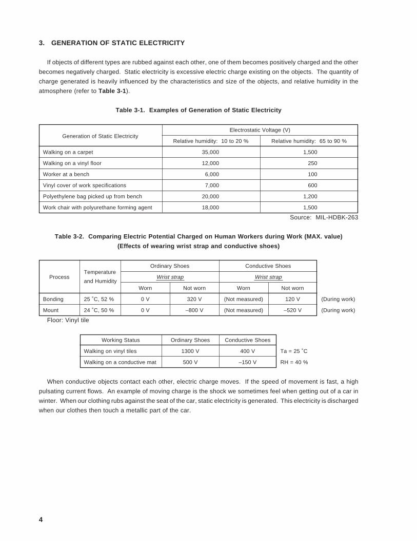
3. GENERATION OF STATIC ELECTRICITY
If objects of different types are rubbed against each other, one of them becomes positively charged and the other
becomes negatively charged. Static electricity is excessive electric charge existing on the objects. The quantity of
charge generated is heavily influenced by the characteristics and size of the objects, and relative humidity in the
atmosphere (refer to Table 3-1 ).
Table 3-1. Examples of Generation of Static Electricity
Generation of Static ElectricityElectrostatic Voltage (V)
Relative humidity: 10 to 20 % Relative humidity: 65 to 90 %
Walking on a carpet 35,000 1,500
Walking on a vinyl floor 12,000 250
Worker at a bench 6,000 100
Vinyl cover of work specifications 7,000 600
Polyethylene bag picked up from bench 20,000 1,200
Work chair with polyurethane forming agent 18,000 1,500
Source: MIL-HDBK-263
Table 3-2. Comparing Electric Potential Charged on Human Workers during Work (MAX. value)
(Effects of wearing wrist strap and conductive shoes)
TemperatureOrdinary Shoes Conductive Shoes
Processand Humidity
Wrist strap Wrist strap
Worn Not worn Worn Not worn
Bonding 25 ˚C, 52 % 0 V 320 V (Not measured) 120 V (During work)
Mount 24 ˚C, 50 % 0 V –800 V (Not measured) –520 V (During work)
Floor: Vinyl tile
Working Status Ordinary Shoes Conductive Shoes
Walking on vinyl tiles 1300 V 400 V Ta = 25 ˚C
Walking on a conductive mat 500 V –150 V RH = 40 %
When conductive objects contact each other, electric charge moves. If the speed of movement is fast, a high
pulsating current flows. An example of moving charge is the shock we sometimes feel when getting out of a car in
winter. When our clothing rubs against the seat of the car, static electricity is generated. This electricity is discharged
when our clothes then touch a metallic part of the car.
5
4. DAMAGE TO SEMICONDUCTOR DEVICES BY ESD
4.1 Why Are Semiconductor Devices Damaged by Electrostatic Discharge?Generally, MOS ICs, FETs, and high-frequency devices are sensitive to static electricity and are easily damaged
by electrostatic discharges. This is because their circuit configuration and structure are susceptible to the damaging
phenomena which will be explained in 4-3.
To protect these devices from damage, they are usually provided with an internal protection circuit in the power
block or input/output block. However, this protection circuit is not omnipotent. In addition, the effect of the protection
circuit differs from one device to another because a number of factors, and so the characteristics, configuration and
dimensions of the protection circuit, and the process of the device, must be taken into consideration when choosing
a protection circuit.
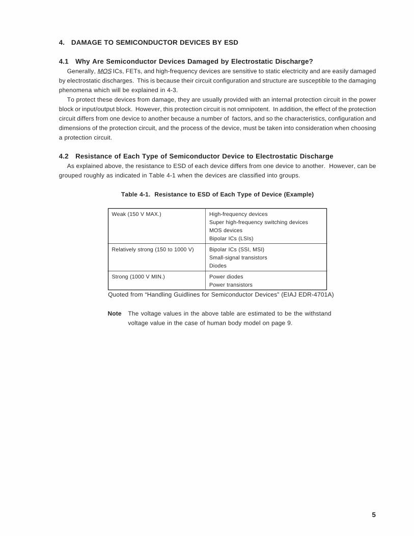
4.2 Resistance of Each Type of Semiconductor Device to Electrostatic DischargeAs explained above, the resistance to ESD of each device differs from one device to another. However, can be
grouped roughly as indicated in Table 4-1 when the devices are classified into groups.
Table 4-1. Resistance to ESD of Each Type of Device (Example)
Weak (150 V MAX.) High-frequency devices
Super high-frequency switching devices
MOS devices
Bipolar ICs (LSIs)
Relatively strong (150 to 1000 V) Bipolar ICs (SSI, MSI)
Small-signal transistors
Diodes
Strong (1000 V MIN.) Power diodes
Power transistors
Quoted from “Handling Guidlines for Semiconductor Devices” (EIAJ EDR-4701A)
Note The voltage values in the above table are estimated to be the withstand
voltage value in the case of human body model on page 9.
6
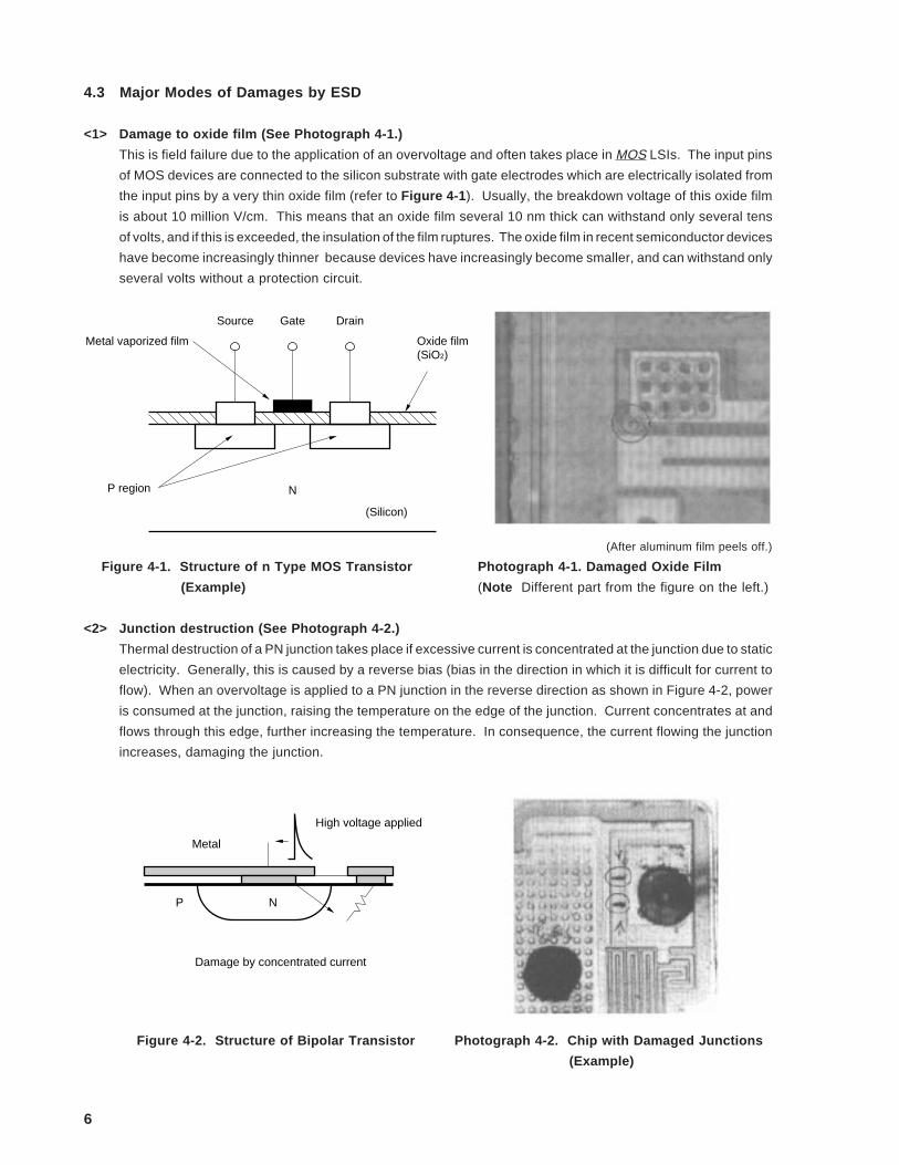
4.3 Major Modes of Damages by ESD
<1> Damage to oxide film (See Photograph 4-1.)
This is field failure due to the application of an overvoltage and often takes place in MOS LSIs. The input pins
of MOS devices are connected to the silicon substrate with gate electrodes which are electrically isolated from
the input pins by a very thin oxide film (refer to Figure 4-1 ). Usually, the breakdown voltage of this oxide film
is about 10 million V/cm. This means that an oxide film several 10 nm thick can withstand only several tens
of volts, and if this is exceeded, the insulation of the film ruptures. The oxide film in recent semiconductor devices
have become increasingly thinner because devices have increasingly become smaller, and can withstand only
several volts without a protection circuit.
(After aluminum film peels off.)
Figure 4-1. Structure of n Type MOS Transistor Photograph 4-1. Damaged Oxide Film
(Example) (Note Different part from the figure on the left.)
<2> Junction destruction (See Photograph 4-2.)
Thermal destruction of a PN junction takes place if excessive current is concentrated at the junction due to static
electricity. Generally, this is caused by a reverse bias (bias in the direction in which it is difficult for current to
flow). When an overvoltage is applied to a PN junction in the reverse direction as shown in Figure 4-2, power
is consumed at the junction, raising the temperature on the edge of the junction. Current concentrates at and
flows through this edge, further increasing the temperature. In consequence, the current flowing the junction
increases, damaging the junction.
Figure 4-2. Structure of Bipolar Transistor Photograph 4-2. Chip with Damaged Junctions
(Example)
Source DrainGate
Metal vaporized film
P region
Oxide film(SiO2)
N
(Silicon)
Metal
P N
High voltage applied
Damage by concentrated current
7
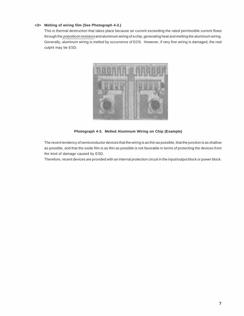
<3> Melting of wiring film (See Photograph 4-3.)
This is thermal destruction that takes place because an current exceeding the rated permissible current flows
through the polysilicon resistors and aluminum wiring of a chip, generating heat and melting the aluminum wiring.
Generally, aluminum wiring is melted by occurrence of EOS. However, if very fine wiring is damaged, the real
culprit may be ESD.
Photograph 4-3. Melted Aluminum Wiring on Chip (Example)
The recent tendency of semiconductor devices that the wiring is as thin as possible, that the junction is as shallow
as possible, and that the oxide film is as thin as possible is not favorable in terms of protecting the devices from
the kind of damage caused by ESD.
Therefore, recent devices are provided with an internal protection circuit in the input/output block or power block.
8
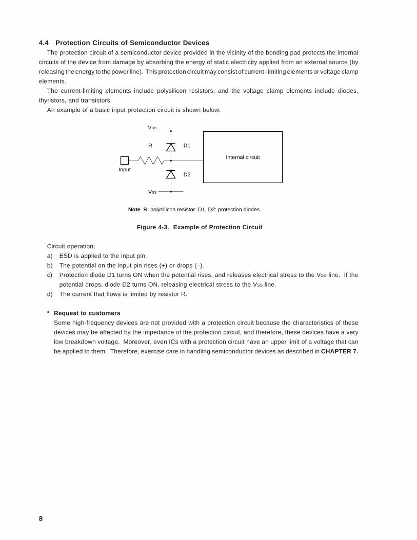
4.4 Protection Circuits of Semiconductor DevicesThe protection circuit of a semiconductor device provided in the vicinity of the bonding pad protects the internal
circuits of the device from damage by absorbing the energy of static electricity applied from an external source (by
releasing the energy to the power line). This protection circuit may consist of current-limiting elements or voltage clamp
elements.
The current-limiting elements include polysilicon resistors, and the voltage clamp elements include diodes,
thyristors, and transistors.
An example of a basic input protection circuit is shown below.
VDD
VSS
R D1
D2
Internal circuit
Input
Note R: polysilicon resistor D1, D2: protection diodes
Figure 4-3. Example of Protection Circuit
Circuit operation:
a) ESD is applied to the input pin.
b) The potential on the input pin rises (+) or drops (–).
c) Protection diode D1 turns ON when the potential rises, and releases electrical stress to the VDD line. If the
potential drops, diode D2 turns ON, releasing electrical stress to the VSS line.
d) The current that flows is limited by resistor R.
* Request to customers
Some high-frequency devices are not provided with a protection circuit because the characteristics of these
devices may be affected by the impedance of the protection circuit, and therefore, these devices have a very
low breakdown voltage. Moreover, even ICs with a protection circuit have an upper limit of a voltage that can
be applied to them. Therefore, exercise care in handling semiconductor devices as described in CHAPTER 7.
9
5. MODELS OF DAMAGE BY ESD
We have discussed how the characteristics of semiconductor devices may be degraded or devices may be
damaged by static electricity in the preceding section (4-3). Electrostatic discharge may take place in a number of
ways. The table below lists some models of damage to semiconductor devices by ESD.
Table 5-1. Representative Damage to Semiconductor Devices by ESD
Description
Charge built up on the human body
is discharged when a part of the
body touches a pin of the device.
The device is damaged by
discharged current if a pin of the
device is grounded.
Charge built up on a metallic object
is discharged when the object
touches a pin of the device.
The device is damaged by
discharged current if a pin of the
device is grounded.
The conductors (such as the chip,
wires, and lead frames) of the
device are charged, and
discharging takes place when a pin
of the device touches equipment, a
jig, or a tool.
The charge built up on the
conductor of the device is
discharged as soon as the device
is grounded, damaging the device.
The surface of the device package
is charged because of friction or
other causes. As a result, static
induction takes place on the
conductive part of the device, and
charge on the conductive part of
the device is discharged
immediately when a pin of the
device comes into contact with
equipment, a jig, or a tool.
The charge built up on the
conductor of the device is
discharged as soon as the device
is grounded, damaging the device.
Model Name
Human Body
Model (HBM)
Machine Model
(MM)
Charged Device
Model (CDM)
Charged Package
Model (CPM)
Note The polarity of charging and current direction shown above are for explanatory purposes and actually show
complicated changes.
++
++
Current I
LSI
Current I
LSI+ +
+ ++
Metallichousing
++
+ +
+
+ +
+
LSI
Current I
Cause (Example)
• Not wearing wrist strap
and conductive shoes
• Wearing clothing which
readily generates static
electricity
• Directly touching pins
with the hand
• Current leaking from
soldering iron
• Leakage current of
equipment, insufficient
grounding, etc.
• Contact of charged
object with pin of
device
• Dropping or touching
charged device on a
metallic object
• Friction at
transportation block of
automatic IC mounter
Figure (Example) Note
++
++
+––
–
––
–
LSI
10
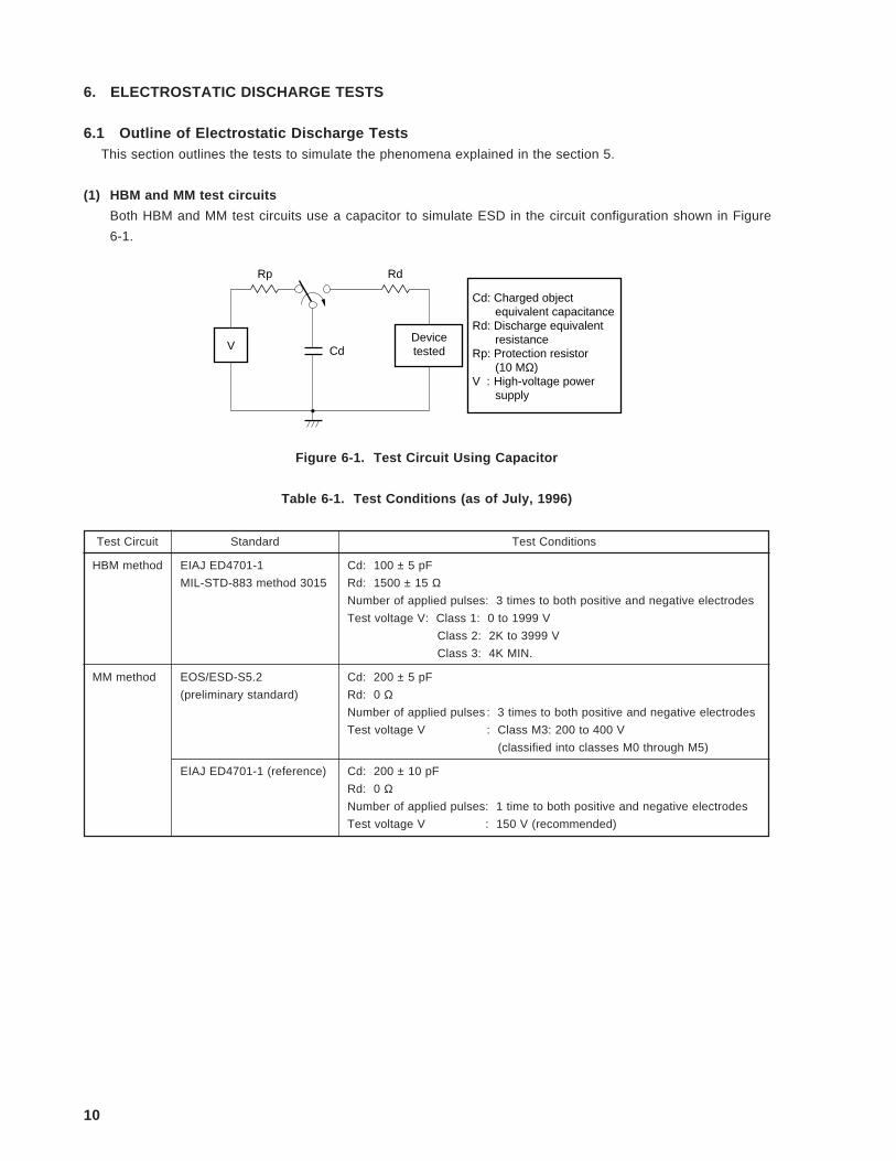
6. ELECTROSTATIC DISCHARGE TESTS
6.1 Outline of Electrostatic Discharge TestsThis section outlines the tests to simulate the phenomena explained in the section 5.
(1) HBM and MM test circuits
Both HBM and MM test circuits use a capacitor to simulate ESD in the circuit configuration shown in Figure
6-1.
V
Rp
Devicetested
Rd
Cd
Cd: Charged object equivalent capacitance Rd: Discharge equivalent resistance Rp: Protection resistor (10 MΩ) V : High-voltage power supply
Figure 6-1. Test Circuit Using Capacitor
Table 6-1. Test Conditions (as of July, 1996)
Test Circuit Standard Test Conditions
HBM method EIAJ ED4701-1 Cd: 100 ± 5 pF
MIL-STD-883 method 3015 Rd: 1500 ± 15 ΩNumber of applied pulses: 3 times to both positive and negative electrodes
Test voltage V: Class 1: 0 to 1999 V
Class 2: 2K to 3999 V
Class 3: 4K MIN.
MM method EOS/ESD-S5.2 Cd: 200 ± 5 pF
(preliminary standard) Rd: 0 ΩNumber of applied pulses : 3 times to both positive and negative electrodes
Test voltage V : Class M3: 200 to 400 V
(classified into classes M0 through M5)
EIAJ ED4701-1 (reference) Cd: 200 ± 10 pF
Rd: 0 ΩNumber of applied pulses: 1 time to both positive and negative electrodes
Test voltage V : 150 V (recommended)
11
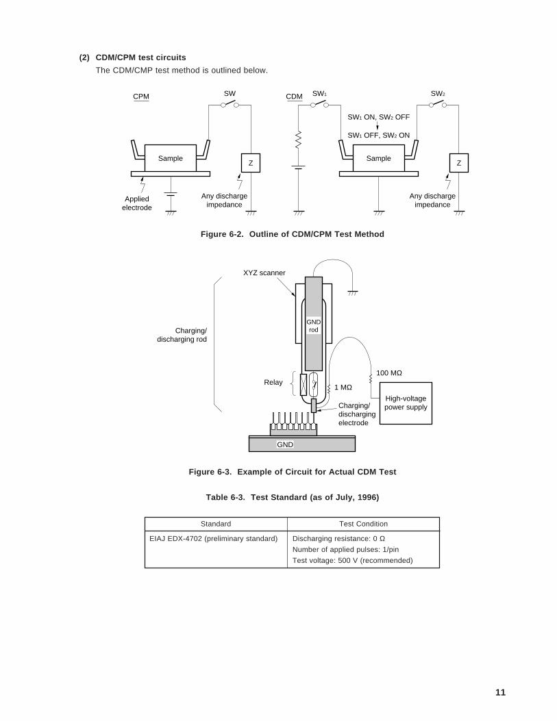
(2) CDM/CPM test circuits
The CDM/CMP test method is outlined below.
ZSample
SW
Appliedelectrode
Any dischargeimpedance
CPM
ZSample
SW2
Any dischargeimpedance
CDM SW1
SW1 ON, SW2 OFF
SW1 OFF, SW2 ON
Figure 6-2. Outline of CDM/CPM Test Method
XYZ scanner
Charging/discharging rod
Relay1 MΩ
100 MΩ
Charging/dischargingelectrode
High-voltagepower supply
GNDrod
GND
Figure 6-3. Example of Circuit for Actual CDM Test
Table 6-3. Test Standard (as of July, 1996)
Standard Test Condition
EIAJ EDX-4702 (preliminary standard) Discharging resistance: 0 ΩNumber of applied pulses: 1/pin
Test voltage: 500 V (recommended)
12
6.2 Reviewing Standards of Electrostatic Discharge TestsBecause the value of a breakdown voltage differs depending on the type of ESD, it is important to specify a
discharging waveform for electrostatic discharge tests. In particular, with the MM method, differences depending on
the test equipment exist because the load resistance is 0 Ω and therefore, the test result is influenced by the wiring
of the machine and impedance of contacts. The existing test standards (such as EIAJ Standard and MIL Standard)
do not adequately specify the discharging current waveform. Consequently, the reviewing and standardizing of
electrostatic discharge tests including the specification of waveforms is currently being carried out in the USA, Europe,
and Japan. It is therefore expected that differences due to the test equipment can be reduced for the HBM test. As
for the MM and CMD tests, however, there is still much international debate, and further exchange of opinions is
necessary.
The progress of reviewing each model is as follows:
<1> HBM test
Because the contents of both the EIAJ EOS and ESD Standards are the same, it is expected that differences
in HBM test equipment will be reduced between the USA and Japan.
<2> MM test
EIAJ specifies the MM test as a test for reference only on the assumption that it will be scrapped in the future
because the results of this test do not match the failure modes in the field. On the other hand, the USA and
Europe are proposing that the MM test be used an official test, by specifying the discharging waveform.
Therefore, the following problems must be solved.
• Japan, USA, and Europe have not yet reached an agreement and exchange of opinions are necessary.
• The currently-used test equipment does not conform to the EOS/ESD Standard.
<3> CDM test
The peak current of the discharging waveform is different in the EIAJ EOS and ESD Standards. Therefore, there
is a difference in the absolute value of the test breakdown voltage, which is expected to pose a problem in the
future.
Therefore, MM and CMD tests must be modified and standardized by official organizations in the future.
6.3 Application of Electrostatic Discharge TestsRepresentative electrostatic discharge tests such as HBM, MM, and CMD exist. Generally speaking, the HBM and
MM tests can reproduce thermal destruction such as junction destruction and melting of wiring, and the CDM test is
suitable for reproduction of electric field destruction, i.e. oxide film destruction.
Common modes of damage to MOS semiconductor devices by ESD are junction destruction and oxide film
destruction. The former can be reproduced by the HBM and MM tests, and the latter can be reproduced by the CMD
tests.
A common form of damage to discrete components by ESD is junction destruction, which can be reproduced by
the HBM and MM tests.
Melting of aluminum wiring can also be often observed in discrete components, but it is considered that this is largely
due to EOS.
13
6.4 NEC’s Electrostatic Discharge TestsThe important points in collecting ESD test data are that the data reflect the actual destruction failure modes in
the field, and that they must conform to official standards. At present, however, only the HBM test satisfies these
conditions, and NEC conducts CDM and MM tests on some models just for reference.
Table 6-1. NEC’s Electrostatic Discharge Tests (as of July, 1996)
Model Corresponding Test Standard Applicable Products
HBM EIAJ ED4701-1 Representative model of each family
MIL-STD-883 method 3015
MM (test for reference) EOS/ESD-S5.2 (preliminary standard) Some models
EIAJ ED4701-1 (test for reference)
CDM (test for reference) EIAJ EDX4702 (preliminary standard) Some models
7. GENERAL POINTS TO BE NOTED ON ESD
The most important countermeasures against static electricity are to prevent the generation of static electricity and
to safely discharge any generated charge (abrupt discharging of charge built up on a semiconductor device leads to
damages to the device). Therefore, the generation of charge because of friction due to vibration during transportation
must be prevented and devices must be handled in appropriate working environments. In addition, workers who
handle semiconductor devices must have sufficient knowledge of the countermeasures against static electricity. This
chapter explains countermeasures against static electricity while packaging semiconductor devices, and general
points to be noted in handling the devices.
14
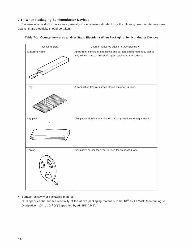
7.1 When Packaging Semiconductor DevicesBecause semiconductor devices are generally susceptible to static electricity, the following basic countermeasures
against static electricity should be taken.
Table 7-1. Countermeasures against Static Electricity When Packaging Semiconductor Devices
Packaging Style Countermeasures against Static Electricity
Magazine case Apart from aluminum magazines and carbon plastic materials, plastic
magazines have an anti-static agent applied to the surface.
Tray A conductive tray (of carbon plastic material) is used.
Dry pack Dissipative aluminum-laminated bag or polyethylene bag is used.
Taping Dissipative carrier tape reel is used for embossed tape.
• Surface resistivity of packaging material
NEC specifies the surface resistivity of the above packaging materials to be 1012 Ω/ MAX. (conforming to
Dissipative –105 to 1012 Ω/ specified by ANSI/EIA541).
15
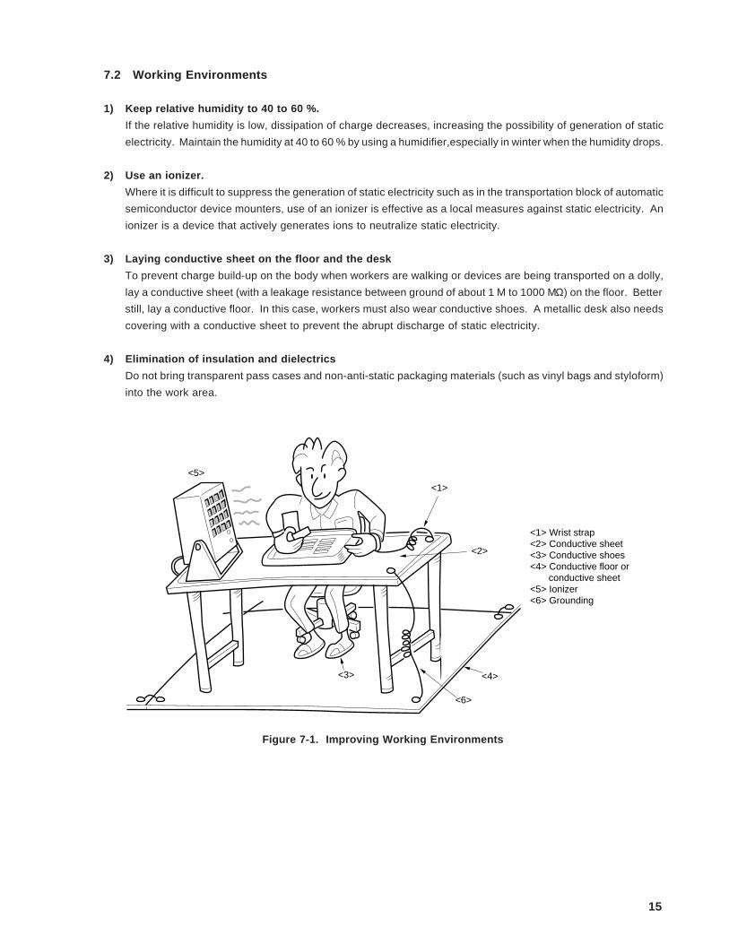
7.2 Working Environments
1) Keep relative humidity to 40 to 60 %.
If the relative humidity is low, dissipation of charge decreases, increasing the possibility of generation of static
electricity. Maintain the humidity at 40 to 60 % by using a humidifier,especially in winter when the humidity drops.
2) Use an ionizer.
Where it is difficult to suppress the generation of static electricity such as in the transportation block of automatic
semiconductor device mounters, use of an ionizer is effective as a local measures against static electricity. An
ionizer is a device that actively generates ions to neutralize static electricity.
3) Laying conductive sheet on the floor and the desk
To prevent charge build-up on the body when workers are walking or devices are being transported on a dolly,
lay a conductive sheet (with a leakage resistance between ground of about 1 M to 1000 MΩ) on the floor. Better
still, lay a conductive floor. In this case, workers must also wear conductive shoes. A metallic desk also needs
covering with a conductive sheet to prevent the abrupt discharge of static electricity.
4) Elimination of insulation and dielectrics
Do not bring transparent pass cases and non-anti-static packaging materials (such as vinyl bags and styloform)
into the work area.
<5>
<1>
<2>
<4>
<6>
<3>
<1> Wrist strap <2> Conductive sheet <3> Conductive shoes <4> Conductive floor or conductive sheet <5> Ionizer <6> Grounding
Figure 7-1. Improving Working Environments
16
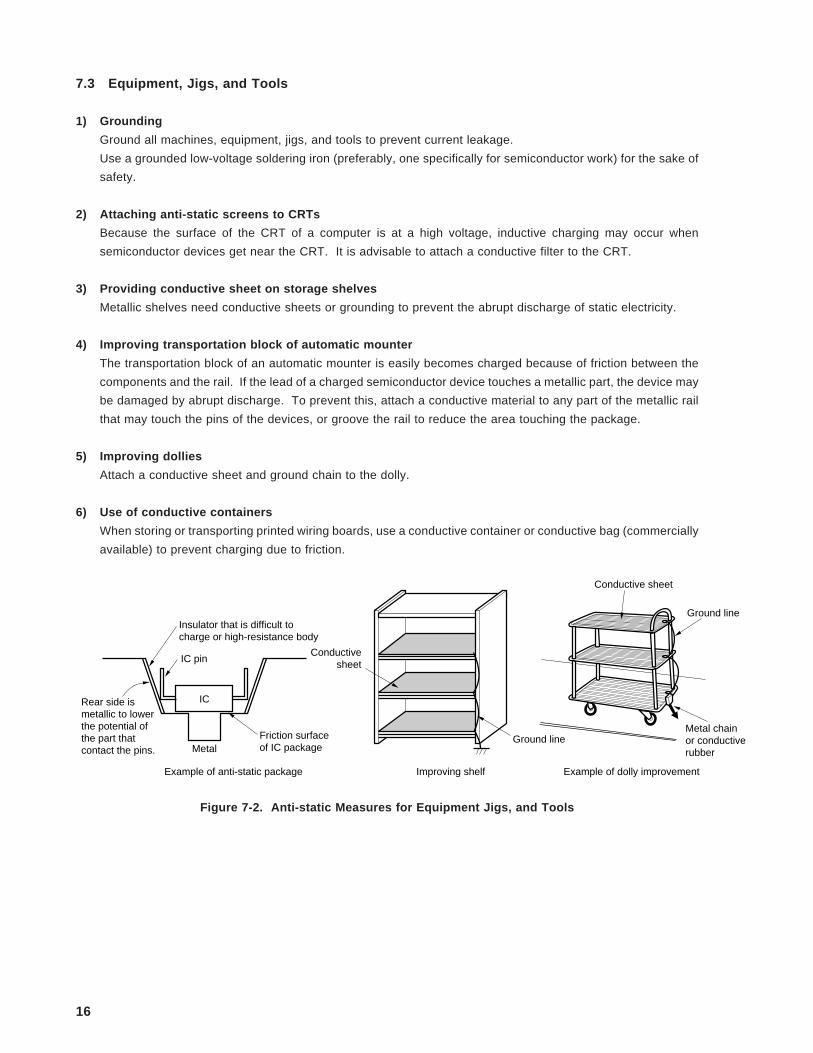
7.3 Equipment, Jigs, and Tools
1) Grounding
Ground all machines, equipment, jigs, and tools to prevent current leakage.
Use a grounded low-voltage soldering iron (preferably, one specifically for semiconductor work) for the sake of
safety.
2) Attaching anti-static screens to CRTs
Because the surface of the CRT of a computer is at a high voltage, inductive charging may occur when
semiconductor devices get near the CRT. It is advisable to attach a conductive filter to the CRT.
3) Providing conductive sheet on storage shelves
Metallic shelves need conductive sheets or grounding to prevent the abrupt discharge of static electricity.
4) Improving transportation block of automatic mounter
The transportation block of an automatic mounter is easily becomes charged because of friction between the
components and the rail. If the lead of a charged semiconductor device touches a metallic part, the device may
be damaged by abrupt discharge. To prevent this, attach a conductive material to any part of the metallic rail
that may touch the pins of the devices, or groove the rail to reduce the area touching the package.
5) Improving dollies
Attach a conductive sheet and ground chain to the dolly.
6) Use of conductive containers
When storing or transporting printed wiring boards, use a conductive container or conductive bag (commercially
available) to prevent charging due to friction.
ICRear side ismetallic to lowerthe potential ofthe part thatcontact the pins.
Insulator that is difficult tocharge or high-resistance body
IC pin
MetalFriction surfaceof IC package
Conductivesheet
Ground line
Conductive sheet
Ground line
Metal chainor conductiverubber
Example of anti-static package Improving shelf Example of dolly improvement
Figure 7-2. Anti-static Measures for Equipment Jigs, and Tools
17
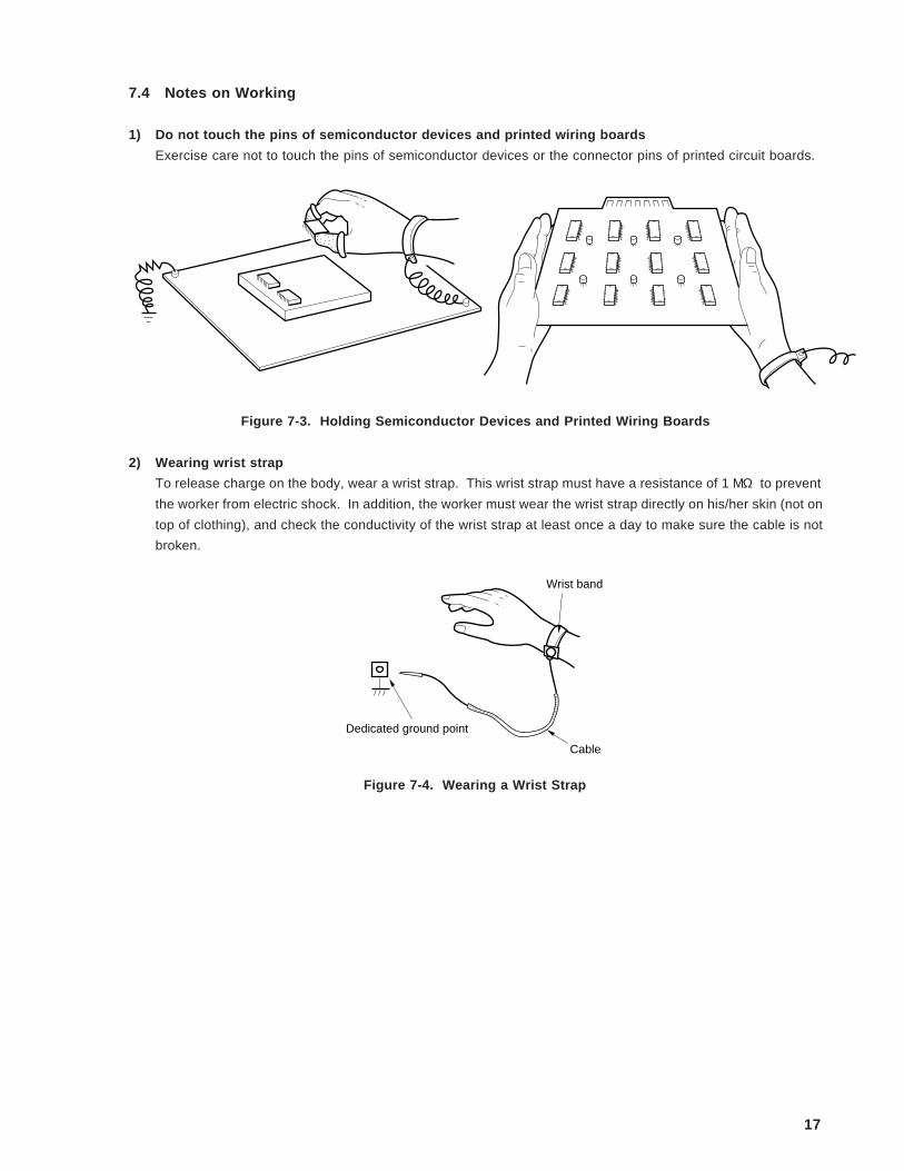
7.4 Notes on Working
1) Do not touch the pins of semiconductor devices and printed wiring boards
Exercise care not to touch the pins of semiconductor devices or the connector pins of printed circuit boards.
Figure 7-3. Holding Semiconductor Devices and Printed Wiring Boards
2) Wearing wrist strap
To release charge on the body, wear a wrist strap. This wrist strap must have a resistance of 1 MΩ to prevent
the worker from electric shock. In addition, the worker must wear the wrist strap directly on his/her skin (not on
top of clothing), and check the conductivity of the wrist strap at least once a day to make sure the cable is not
broken.
Wrist band
Dedicated ground point
Cable
Figure 7-4. Wearing a Wrist Strap
18
Reference documents
1) MIL HDBK-263 : ELECTROSTATIC DISCHARGE CONTROL HANDBOOK OF PROTECTION FOR ELEC-
TRICAL AND ELECTRONIC PARTS, ASSEMBLIES, AND EQUIPMENT
2) EIAJ EDR-4701A : HANDLING GUIDELINES FOR SEMICONDUCTOR DEVICES
(Electronic Industries Association of Japan)
3) EIAJ ED-4701-1 : ENVIRONMENTAL AND ENDURANCE TEST METHODS FOR SEMICONDUCTOR
DEVICES (AMENDMENT 1)
(Electronic Industries Association of Japan)
4) EIAJ EDX-4702 : TEST METHODS OF CHARGED DEVICE MODEL ELECTROSTATIC DISCHARGE
(Electronic Industries Association of Japan)
5) NIS-M-1801 : ELECTROSTATIC COUNTERMEASURE GUIDELINES
(NEC Corporation)
6) RCJS-0901A-1996: GLOSSARY OF TERMS USED IN ELECTROSTATIC DISCHARGE
(RCJ)
7) SES-C-0157 : SEMICONDUCTOR TECHNICAL TERMS
(NEC Corporation)
8) R-6-ES-01 : TECHNIQUES FOR PREVENTING DAMAGE TO SEMICONDUCTOR DEVICES BY
ELECTROSTATIC DISCHARGE
(RCJ)
9) MEI-1202 : GUIDE TO QUALITY ASSURANCE FOR SEMICONDUCTOR DEVICES
(NEC Corporation)
19
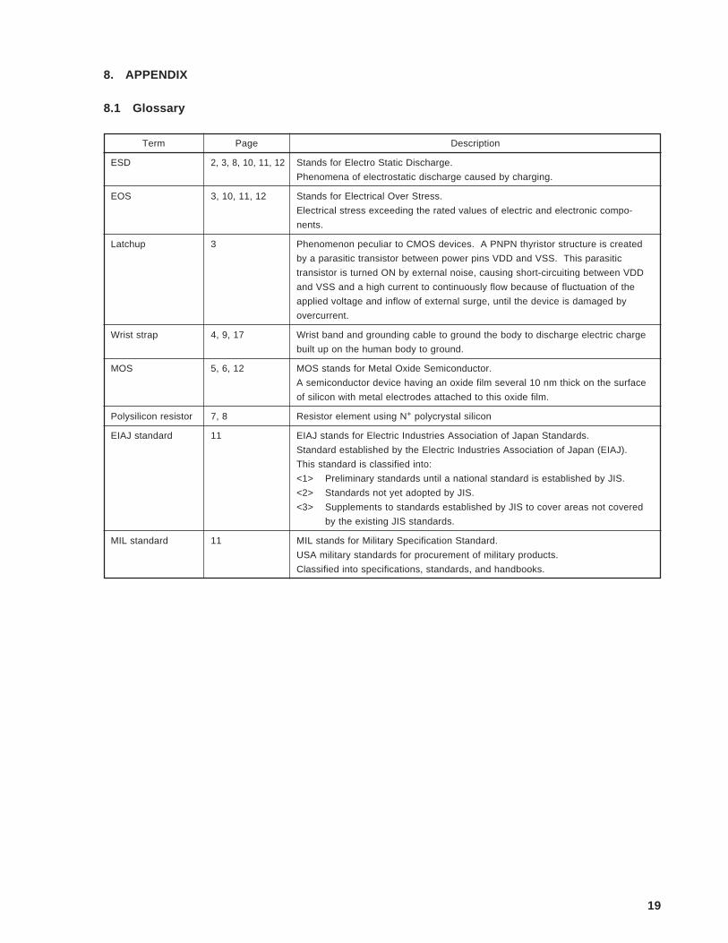
8. APPENDIX
8.1 Glossary
Term Page Description
ESD 2, 3, 8, 10, 11, 12 Stands for Electro Static Discharge.
Phenomena of electrostatic discharge caused by charging.
EOS 3, 10, 11, 12 Stands for Electrical Over Stress.
Electrical stress exceeding the rated values of electric and electronic compo-
nents.
Latchup 3 Phenomenon peculiar to CMOS devices. A PNPN thyristor structure is created
by a parasitic transistor between power pins VDD and VSS. This parasitic
transistor is turned ON by external noise, causing short-circuiting between VDD
and VSS and a high current to continuously flow because of fluctuation of the
applied voltage and inflow of external surge, until the device is damaged by
overcurrent.
Wrist strap 4, 9, 17 Wrist band and grounding cable to ground the body to discharge electric charge
built up on the human body to ground.
MOS 5, 6, 12 MOS stands for Metal Oxide Semiconductor.
A semiconductor device having an oxide film several 10 nm thick on the surface
of silicon with metal electrodes attached to this oxide film.
Polysilicon resistor 7, 8 Resistor element using N+ polycrystal silicon
EIAJ standard 11 EIAJ stands for Electric Industries Association of Japan Standards.
Standard established by the Electric Industries Association of Japan (EIAJ).
This standard is classified into:
<1> Preliminary standards until a national standard is established by JIS.
<2> Standards not yet adopted by JIS.
<3> Supplements to standards established by JIS to cover areas not covered
by the existing JIS standards.
MIL standard 11 MIL stands for Military Specification Standard.
USA military standards for procurement of military products.
Classified into specifications, standards, and handbooks.
20
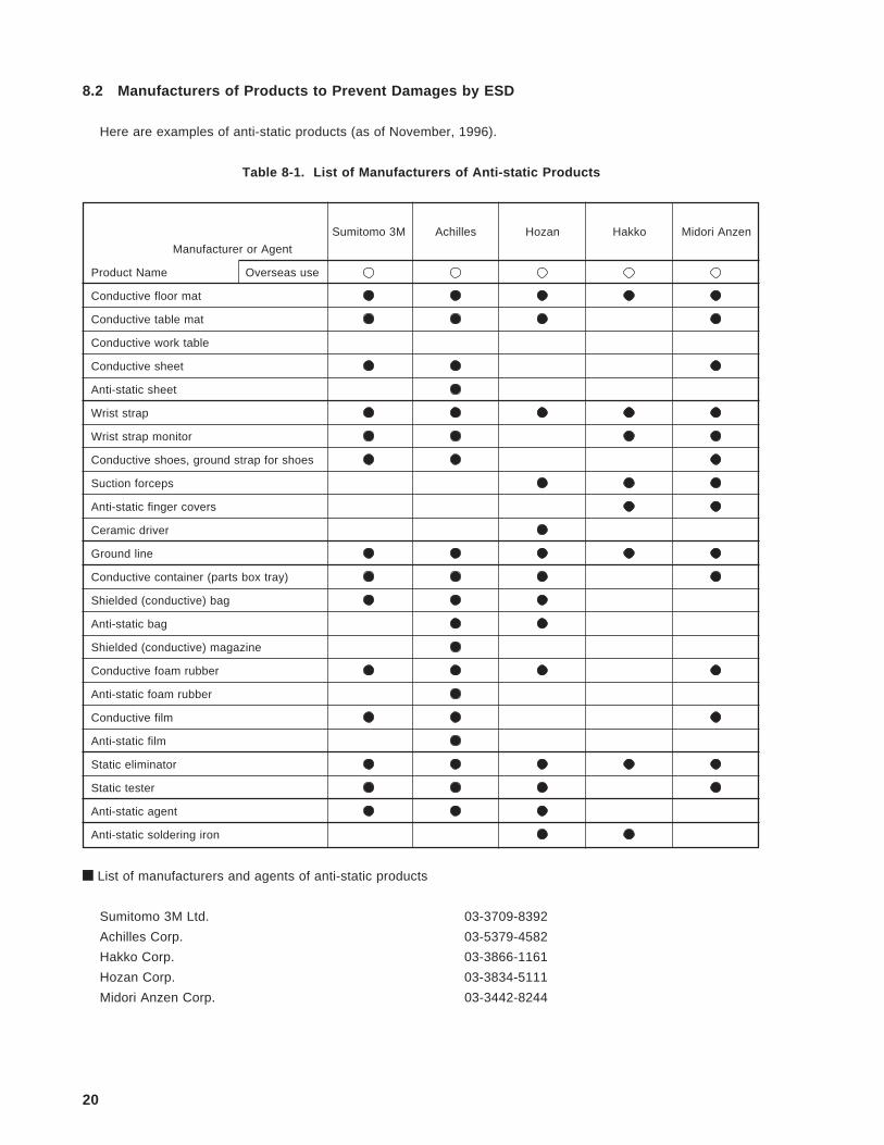
8.2 Manufacturers of Products to Prevent Damages by ESD
Here are examples of anti-static products (as of November, 1996).
Table 8-1. List of Manufacturers of Anti-static Products
Sumitomo 3M Achilles Hozan Hakko Midori Anzen
Manufacturer or Agent
Product Name Overseas use
Conductive floor mat
Conductive table mat
Conductive work table
Conductive sheet
Anti-static sheet
Wrist strap
Wrist strap monitor
Conductive shoes, ground strap for shoes
Suction forceps
Anti-static finger covers
Ceramic driver
Ground line
Conductive container (parts box tray)
Shielded (conductive) bag
Anti-static bag
Shielded (conductive) magazine
Conductive foam rubber
Anti-static foam rubber
Conductive film
Anti-static film
Static eliminator
Static tester
Anti-static agent
Anti-static soldering iron
List of manufacturers and agents of anti-static products
Sumitomo 3M Ltd. 03-3709-8392
Achilles Corp. 03-5379-4582
Hakko Corp. 03-3866-1161
Hozan Corp. 03-3834-5111
Midori Anzen Corp. 03-3442-8244
No part of this document may be copied or reproduced in any form or by any means without the prior writtenconsent of NEC Corporation. NEC Corporation assumes no responsibility for any errors which may appear inthis document.NEC Corporation does not assume any liability for infringement of patents, copyrights or other intellectualproperty rights of third parties by or arising from use of a device described herein or any other liability arisingfrom use of such device. No license, either express, implied or otherwise, is granted under any patents,copyrights or other intellectual property rights of NEC Corporation or of others.
M4A 96.10