Embed Size (px)
Citation preview

ARTICLE
Chemical trends of deep levels in van der WaalssemiconductorsPenghong Ci 1,2, Xuezeng Tian 3, Jun Kang4, Anthony Salazar1, Kazutaka Eriguchi1, Sarah Warkander 1,
Kechao Tang1, Jiaman Liu1, Yabin Chen1,5, Sefaattin Tongay6, Wladek Walukiewicz2, Jianwei Miao 3,
Oscar Dubon1,2 & Junqiao Wu 1,2✉
Properties of semiconductors are largely defined by crystal imperfections including native
defects. Van der Waals (vdW) semiconductors, a newly emerged class of materials, are no
exception: defects exist even in the purest materials and strongly affect their electrical,
optical, magnetic, catalytic and sensing properties. However, unlike conventional semi-
conductors where energy levels of defects are well documented, they are experimentally
unknown in even the best studied vdW semiconductors, impeding the understanding and
utilization of these materials. Here, we directly evaluate deep levels and their chemical trends
in the bandgap of MoS2, WS2 and their alloys by transient spectroscopic study. One of the
deep levels is found to follow the conduction band minimum of each host, attributed to the
native sulfur vacancy. A switchable, DX center - like deep level has also been identified,
whose energy lines up instead on a fixed level across different hosts, explaining a persistent
photoconductivity above 400 K.
https://doi.org/10.1038/s41467-020-19247-1 OPEN
1 Department of Materials Science and Engineering, University of California, Berkeley, CA 94720, USA. 2Materials Sciences Division, Lawrence BerkeleyNational Laboratory, Berkeley, CA 94720, USA. 3 Department of Physics & Astronomy and California NanoSystems Institute, University of California, LosAngeles, CA, USA. 4 Beijing Computational Science Research Center, Beijing, China. 5 School of Aerospace Engineering, Beijing Institute of Technology,Beijing, China. 6 School for Engineering of Matter, Transport, and Energy, Arizona State University, Tempe, AZ 85287, USA. ✉email: [email protected]
NATURE COMMUNICATIONS | (2020) 11:5373 | https://doi.org/10.1038/s41467-020-19247-1 | www.nature.com/naturecommunications 1
1234
5678
90():,;
Defects with energies falling within the bandgap may act asa trap or emitter of free charge carriers1, a site for excitonrecombination2, and a center to scatter electrons or
phonons3. In conventional semiconductors, native defects such asvacancies introduce levels close to the middle of the bandgapwhen the material is more covalently bonded, or close to the bandedges when the material is more ionically bonded, resulting in theformer materials being defect sensitive while the latter materialsare relatively defect tolerant4. Comparing positions of defectlevels across different host materials helps to reveal chemicaltrends that inform defect models with broad impact. For example,the deep level associated with a given impurity5 or native defect6
tends to lie universally at a fixed energy position with respect tothe vacuum level even when doped in different semiconductors,which can be used to determine band alignments of the hostmaterials; equilibrium native defects tend to drive the Fermi leveltoward a stabilization position, and this position with respect tothe bandgap can be used as a descriptor of doping propensity anddoping limit of the semiconductor7; the DX center, an metastabledefect switchable between deep and shallow states, dominates thefree electron density in III-V semiconductor alloys8. It is criticalto ask whether such insights and knowledge attained in studyingconventional semiconductors are applicable in vdW materials.New effects of defects may emerge because the layered nature ofvdW materials allows stronger lattice relaxation as well as newtypes of defects such as intercalated atoms.Scanning tunneling microscopy (STM) is able to experi-
mentally visualize various types of defects on the surface andrelate these imperfections to electronic structures in vdWcrystals9, in particular for the most abundant native pointdefects that play a critical role in their electrical10–13, optical2,magnetic14, catalytic15 and sensing properties16. However, STMstudies have led to inconsistency on the defect types withtransmission electron microscopy investigations, as well asdiscrepancy in signatures of defect-induced mid-gap statesfrom theoretical calculations1,3,17–21, largely because of uncleardifferentiation of STM contrast between the metal and chal-cogen sublattices and the complicated convolution of electronicand geometric structures9. Furthermore, it shows very limitedcapability in detecting defects beneath the surface.In this work, we use deep level transient spectroscopy (DLTS),
a high-frequency capacitance transient thermal scanningmethod22,23, to characterize electronic structures of the deep trapsinside the bandgap of vdW semiconductors, particularly MoS2,WS2 and their alloys, including their energy positions and capturecross sections. Combined with atomic-resolution scanningtransmission electron microscopy and first-principles calcula-tions, one of the deep levels determined by DLTS is identified assulfur vacancies, whose energy position follows the conductionband edge in the host materials, distinct from vacancy defects intraditional group III-V semiconductors. A metastable DX centeris identified in these vdW semiconductors, featuring a persistentphotoconductivity above 400 K and explaining the chemical trendof native electron concentration in the hosts.
ResultsDLTS devices and DLTS spectra. Mechanically exfoliated, mul-tilayer (~ 50 nm) flakes of freshly grown Mo1−xWxS2 (x= 0, 0.4,0.7, 1) crystals were made into two-terminal Schottky-Ohmicdevices (Fig. 1a). The Schottky contact was formed by dry-stamping freshly exfoliated flakes onto pre-deposited Pt electro-des and confirmed by the I–V and C–V curves shown in Fig. 1e, f,both of which show the n-type conductivity of MoS2. Thismaximally protects the depletion region at the Schottky contactagainst contamination and damage24, as it is at this region where
the deep levels trap and emit charge carriers during the DLTSmeasurement. The measured total capacitance (SupplementaryFig. 10) is composed of that of the DLTS device (Cdevice) and thestray capacitance (Cstray) connected in parallel. The latter,although with a large value, is insensitive to the external differ-ential voltage (Supplementary Fig. 10), hence the variation ofcapacitance under the biased voltage indeed probes the former(Fig. 1f).The depletion width at the Schottky junction (~ 20 nm, the
shadow in Fig. 1d), hence the capacitance (Fig. 1c), is initially heldconstant by a steady-state reverse bias (VR=−0.5 V, stage ①)23.An opposite voltage pulse (VP) is then added onto VR, reducingthe depletion width (as evidenced by the increased capacitance atless-negative voltage, Fig. 1f), and allowing the traps in the initialdepletion region to be filled with free electrons (stage ②)23. Whenthe initial, constant bias is restored, the return of the capacitanceto the steady-state value is characterized by a transient (stage ③)related to the emission of majority carriers from the deep traps inthe material. The capacitance difference within a rate window(between the pre-set t2 and t1 in Fig. 1c)22 reaches the maximumat a specific temperature. The emission rate (en) in stage ③
depends exponentially on temperature via the trapping energylevel (Ei) measured from the conduction band minimum (CBM,ECB)22,
enT2
¼ Kσn exp � ECB � Eij jkBT
� �ð1Þ
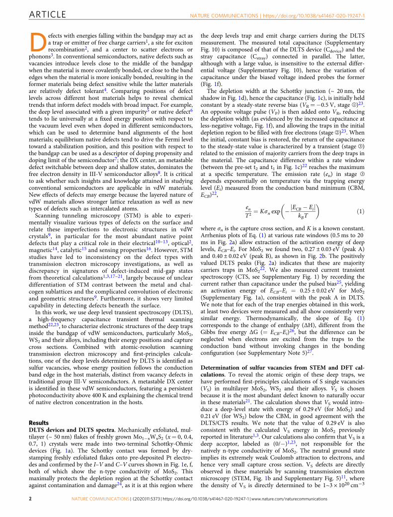
where σn is the capture cross section, and K is a known constant.Arrhenius plots of Eq. (1) at various rate windows (0.5 ms to 20ms in Fig. 2a) allow extraction of the activation energy of deeplevels, ECB–Ei. For MoS2 we found two, 0.27 ± 0.03 eV (peak A)and 0.40 ± 0.02 eV (peak B), as shown in Fig. 2b. The positivelyvalued DLTS peaks (Fig. 2a) indicates that these are majoritycarriers traps in MoS222. We also measured current transientspectroscopy (CTS, see Supplementary Fig. 1) by recording thecurrent rather than capacitance under the pulsed bias25, yieldingan activation energy of ECB–Ei = 0.25 ± 0.02 eV for MoS2(Supplementary Fig. 1a), consistent with the peak A in DLTS.We note that for each of the trap energies obtained in this work,at least two devices were measured and all show consistently verysimilar energy. Thermodynamically, the slope of Eq. (1)corresponds to the change of enthalpy (ΔH), different from theGibbs free energy ΔG (= ECB–Ei)26, but the difference can beneglected when electrons are excited from the traps to theconduction band without invoking changes in the bondingconfiguration (see Supplementary Note 5)27.
Determination of sulfur vacancies from STEM and DFT cal-culations. To reveal the atomic origin of these deep traps, wehave performed first-principles calculations of S single vacancies(VS) in multilayer MoS2, WS2 and their alloys. VS is chosenbecause it is the most abundant defect known to naturally occurin these materials21. The calculation shows that VS would intro-duce a deep-level state with energy of 0.29 eV (for MoS2) and0.21 eV (for WS2) below the CBM, in good agreement with theDLTS/CTS results. We note that the value of 0.29 eV is alsoconsistent with the calculated VS energy in MoS2 previouslyreported in literature1,3. Our calculations also confirm that VS is adeep acceptor, labeled as (0/−)1,23, not responsible for thenatively n-type conductivity of MoS2. The neutral ground stateimplies its extremely weak Coulomb attraction to electrons, andhence very small capture cross section. VS defects are directlyobserved in these materials by scanning transmission electronmicroscopy (STEM, Fig. 1b and Supplementary Fig. 5)11, wherethe density of VS is directly determined to be 1~3 × 1020 cm−3
ARTICLE NATURE COMMUNICATIONS | https://doi.org/10.1038/s41467-020-19247-1
2 NATURE COMMUNICATIONS | (2020) 11:5373 | https://doi.org/10.1038/s41467-020-19247-1 | www.nature.com/naturecommunications

0.00 0.01 0.02 0.03
–0.4
–0.2
0.0
Cap
acita
nce
(a.u
.)
Time (s)
Vol
tage
(V
)
VR
VP
VR
300 K
t1 t2
qVR-
+
deep traps
- - -
EFm
EFn
+ ECB
EVB
Ei
Electron emission
-
- - - --
–0.30 –0.15 0.00 0.15 0.30
0.1
1
10
100
Cur
rent
(μA
)
Voltage (V)
380 K 350 K320 K 290 K260 K 230 K
c
f
a e
b
d
Au / Ti
Pt / Ti
MoS2
i
Substrate: SiO2
PtMoS2 Ti
Measurement
–0.4 –0.2 0.0
ΔC (
pF)
Voltage (V)
380 K
320 K
260 K
200 K
5 pF
13
3
1
2
2
Fig. 1 Materials and devices for transient spectroscopic study of defects. a Schematic and optical image (scale bar: 20 μm) of an asymmetric MoS2device for DLTS, with Schottky contact (MoS2/Pt/Ti) on the bottom and Ohmic contact (Au/Ti/MoS2) on the top. b Aberration-corrected STEM image ofa monolayer MoS2 exfoliated from the materials used for devices. Red arrows highlight S vacancies (VS). Scale bar, 1 nm. c Capacitance transient (bottom)in response to a pulsed change in bias voltage (top). d Band bending of the Schottky junction (MoS2/Pt), illustrating the electron trapping (②) and emissionprocess (③) of deep traps in the depletion region (shaded). VR tunes the Fermi level of the n-type MoS2 (EFn) with respect to that of the metal contact(EFm). e & f, Temperature-dependent I–V and C–V curves confirming the Schottky-Ohmic contacts.
a
b d
–2 –1 0 1 2
Total Mo 4d S 3p
DO
S (
a.u.
)
Energy (eV)
VS
100 200 300 400
DLT
S s
igna
l (a.
u.)
Temperature (K)
20 ms
10 ms
5.0 ms
2.0 ms
1.0 ms
0.5 ms
AB
3.5 4.0 4.5 5.0 5.5
5
6
7
8
9
ln(T
2 /e
n) (
a.u.
)
1000/T (1/K)
A: 0.27 eV(VS)
B: 0.40 eV(DX centers )
c
MoS2
VS(exp.)
EDX
VS (cal.)
Mo = 0.6 Mo = 0.3 WS2–5.6
–5.2
–4.8
–4.4
Ene
rgy
to v
acuu
m (
eV)
Fig. 2 Deep levels and their alignment in vdW crystals. a DLTS signal of a MoS2 device at different rate windows and b the resultant Arrhenius plots todetermine the activation energies. c Conduction and valence band edge alignment calculated with respect to the vacuum level, and positions of deep levelexperimentally identified in this work. Solid black lines: CBM and VBM in bulk crystals from our DFT calculations; red bars: deep levels attributed to VS
measured by DLTS and CTS; blue bars: DX center levels determined by DLTS and PPC (dashed blue line is guide to the eye); green bars: DFT-calculated VS
levels. d density of states (DOS) for multilayer MoS2 with VS. Inset: real space distribution of the wavefunction of VS state. The purple and yellow spheresrepresent Mo and S atoms, respectively.
NATURE COMMUNICATIONS | https://doi.org/10.1038/s41467-020-19247-1 ARTICLE
NATURE COMMUNICATIONS | (2020) 11:5373 | https://doi.org/10.1038/s41467-020-19247-1 | www.nature.com/naturecommunications 3
(Supplementary Fig. 4), on the same order of those reported inliterature3,21. The STEM study also confirms that VS is thedominant point defects, and no other defects or impurities weredetected in the materials. We note that akin to conventionalsemiconductors, not all of these VS are electronically active(Supplementary Fig. 6); in fact, deep traps can be highly passi-vated or compensated, as observed in GaN and GaAs28,29.
To reveal the chemical trend of the VS level in different vdWsemiconductors, Mo0.6W0.4S2, Mo0.3W0.7S2, and WS2 were alsosynthesized and then assembled into Schottky devices for similarDLTS/CTS measurements (Supplementary Fig. 1). All of thesematerials exhibit at least one deep level, akin to the featureA observed in MoS2, with an energy level below the CBM of thehost material of 0.29 ± 0.02 eV, 0.31 ± 0.02 eV and 0.26 ± 0.04 eV(red bars in Fig. 2c), respectively. These energy levels are all ingood agreement with the DFT calculated VS levels, as shown bythe green bars in Fig. 2c and the refined band structure with VS inSupplementary Fig. 8.Some deep levels in different isovalent materials line up at a
fixed position with respect to the vacuum level, such as oxygendopant or Ga dangling bond in different GaAs1−xPx alloys6,30. Incontrast, the red bars in Fig. 2c show that as the W fractionincreases in Mo1−xWxS2, the energy level of VS shifts mono-tonically toward the vacuum level; that is, the VS level largelyfollows the CBM of the host. This is understandable because, asshown in the partial density of states plot in Fig. 2d, the VS stateoriginates mostly from the 4d (5d) orbitals of the Mo (W) atoms,rather than the S atoms, sharing the same orbital composition asthe CBM31,32. Following this finding, anion impurities (such asoxygen) substituting S are predicted to create deep levels alsoabout 0.3 eV below the CBM of the host (see SupplementaryFig. 7), because it is known that highly electronegative,substitutional dopants tend to have similar wavefunctions asthose of ideal vacancies6. The electron capture cross section (σn)of VS is evaluated from Eq. (1) to be ~3.6 × 10⁻¹⁸ cm2 in MoS2,using the thermal velocity effective mass (0.57 mo) and effectivedensity of states mass (0.50 mo) obtained from our DFTcalculation and literature (see Supplementary Note 1). This valueis small but comparable to that of Zn acceptor level in Si and Cuacceptor level in Ge23,33.
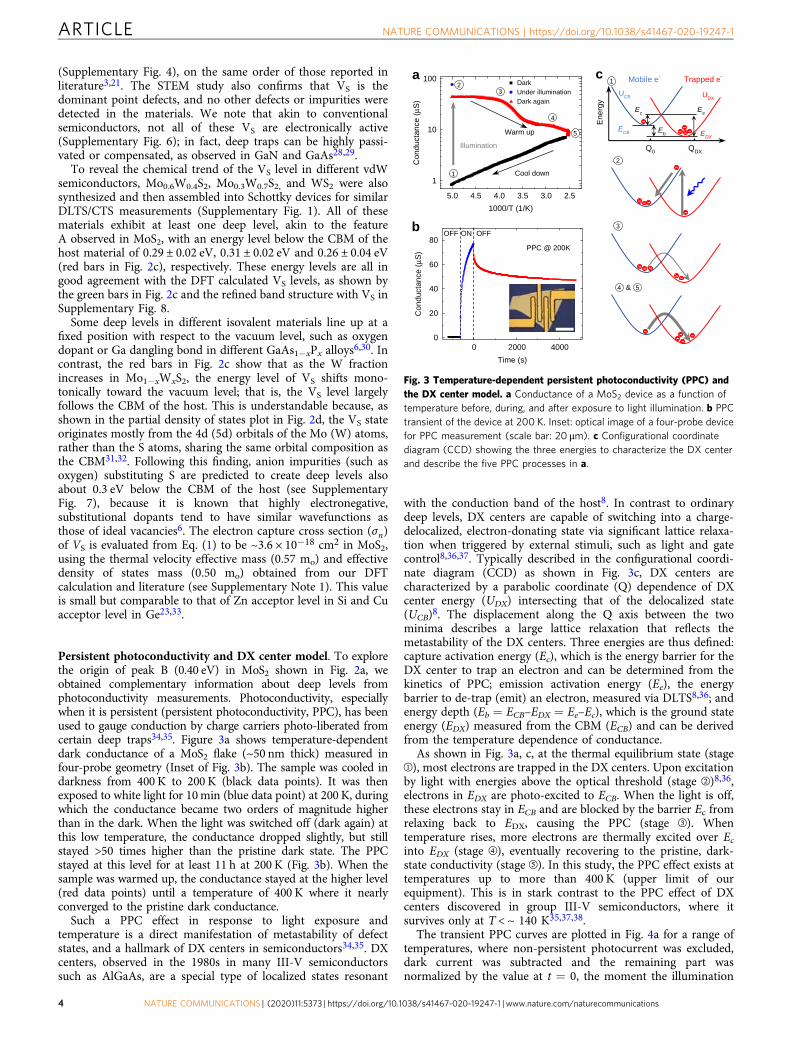
Persistent photoconductivity and DX center model. To explorethe origin of peak B (0.40 eV) in MoS2 shown in Fig. 2a, weobtained complementary information about deep levels fromphotoconductivity measurements. Photoconductivity, especiallywhen it is persistent (persistent photoconductivity, PPC), has beenused to gauge conduction by charge carriers photo-liberated fromcertain deep traps34,35. Figure 3a shows temperature-dependentdark conductance of a MoS2 flake (~50 nm thick) measured infour-probe geometry (Inset of Fig. 3b). The sample was cooled indarkness from 400 K to 200 K (black data points). It was thenexposed to white light for 10min (blue data point) at 200 K, duringwhich the conductance became two orders of magnitude higherthan in the dark. When the light was switched off (dark again) atthis low temperature, the conductance dropped slightly, but stillstayed >50 times higher than the pristine dark state. The PPCstayed at this level for at least 11 h at 200 K (Fig. 3b). When thesample was warmed up, the conductance stayed at the higher level(red data points) until a temperature of 400 K where it nearlyconverged to the pristine dark conductance.Such a PPC effect in response to light exposure and
temperature is a direct manifestation of metastability of defectstates, and a hallmark of DX centers in semiconductors34,35. DXcenters, observed in the 1980s in many III-V semiconductorssuch as AlGaAs, are a special type of localized states resonant
with the conduction band of the host8. In contrast to ordinarydeep levels, DX centers are capable of switching into a charge-delocalized, electron-donating state via significant lattice relaxa-tion when triggered by external stimuli, such as light and gatecontrol8,36,37. Typically described in the configurational coordi-nate diagram (CCD) as shown in Fig. 3c, DX centers arecharacterized by a parabolic coordinate (Q) dependence of DXcenter energy (UDX) intersecting that of the delocalized state(UCB)8. The displacement along the Q axis between the twominima describes a large lattice relaxation that reflects themetastability of the DX centers. Three energies are thus defined:capture activation energy (Ec), which is the energy barrier for theDX center to trap an electron and can be determined from thekinetics of PPC; emission activation energy (Ee), the energybarrier to de-trap (emit) an electron, measured via DLTS8,36; andenergy depth (Eb = ECB–EDX = Ee–Ec), which is the ground stateenergy (EDX) measured from the CBM (ECB) and can be derivedfrom the temperature dependence of conductance.As shown in Fig. 3a, c, at the thermal equilibrium state (stage
①), most electrons are trapped in the DX centers. Upon excitationby light with energies above the optical threshold (stage ②)8,36,electrons in EDX are photo-excited to ECB. When the light is off,these electrons stay in ECB and are blocked by the barrier Ec fromrelaxing back to EDX, causing the PPC (stage ③). Whentemperature rises, more electrons are thermally excited over Ecinto EDX (stage ④), eventually recovering to the pristine, dark-state conductivity (stage ⑤). In this study, the PPC effect exists attemperatures up to more than 400 K (upper limit of ourequipment). This is in stark contrast to the PPC effect of DXcenters discovered in group III-V semiconductors, where itsurvives only at T < ~ 140 K35,37,38.
The transient PPC curves are plotted in Fig. 4a for a range oftemperatures, where non-persistent photocurrent was excluded,dark current was subtracted and the remaining part wasnormalized by the value at t = 0, the moment the illumination
a c
b
5.0 4.5 4.0 3.5 3.0 2.5
1
10
100 DarkUnder illuminationDark again
Con
duct
ance
(μS
)C
ondu
ctan
ce (
μS)
1000/T (1/K)
Illumination
Cool down
Warm up
0 2000 40000
20
40
60
80
Time (s)
OFF ON OFF
PPC @ 200K
Eb
----
---
Mobile e- Trapped e-
UCB UDX
Ec Ee
Q0 QDX
Ene
rgy
&
--- --
-
-
---
--
-
EDX
ECB
4 5
3
2
5
4
1
32
1
Fig. 3 Temperature-dependent persistent photoconductivity (PPC) andthe DX center model. a Conductance of a MoS2 device as a function oftemperature before, during, and after exposure to light illumination. b PPCtransient of the device at 200 K. Inset: optical image of a four-probe devicefor PPC measurement (scale bar: 20 μm). c Configurational coordinatediagram (CCD) showing the three energies to characterize the DX centerand describe the five PPC processes in a.
ARTICLE NATURE COMMUNICATIONS | https://doi.org/10.1038/s41467-020-19247-1
4 NATURE COMMUNICATIONS | (2020) 11:5373 | https://doi.org/10.1038/s41467-020-19247-1 | www.nature.com/naturecommunications

is terminated. Note that in order to reset the initial dark currentbefore taking each of these PPC curves, the samples were kept at400 K for at least one day in a high vacuum (~10−6 torr) to drainthe extra electrons in ECB. We see that, consistent with the DXcenter model (Fig. 3), high temperature expedites the kinetics ofthe PPC decay. Following the treatment in literature, the PPC canbe well described by the stretched-exponential equation34,35:
IPPC tð Þ=IPPC 0ð Þ ¼ exp½�ðt=τÞβ� ð2Þ
where τ is the characteristic decay time constant, β is a decayindex with a value between 0 and 1. Because of the underlyingthermal activation process, the temperature dependence of τ isrelated to the trap barrier viaτ / expðEc=kBTÞ34,35. Arrheniusplots of the temperature-dependent τ yield Ec of 0.28 ± 0.02 eV forMoS2 and 0.17 ± 0.02 eV for Mo0.3W0.7S2 (Fig. 4b and Supple-mentary Fig. 3). These values are higher than Ec (~0.14 eV) of DXcenters reported in the Se-doped AlGaAs system8, presumablybecause the layered structure of the vdW materials allows largerlattice relaxation than the tetrahedral structure of AlGaAs. Thehigher Ec is also responsible for the extension of PPC to muchhigher temperatures.The energy Eb (= ECB–EDX) characterizes the thermodynamic
energy depth of the DX center, and was extracted from Arrheniusplots of the dark conductance of the sample (SupplementaryFig. 3). Values of Eb= 0.12 eV and 0.30 eV were found for MoS2and Mo0.3W0.7S2, respectively. Adding Eb to Ec gives Ee, theemission barrier, of 0.39 eV and 0.47 eV for MoS2 andMo0.3W0.7S2, respectively. These values are in very goodagreement with the energies of peak B measured in DLTS forMoS2 (0.40 ± 0.02 eV) and Mo0.3W0.7S2 (0.47 ± 0.02 eV). There-fore, we attribute the peak B measured in DLTS to emission of
electrons from the DX centers. We note that, unlike regular deeplevels (such as the VS state) which have no capture/emissionbarriers, for DX centers, the Arrhenius plot of the DLTS spectrumextracts the emission barrier Ee (Figs. 2c and 3c), rather than Ebwhich is the separation of EDX directly measured from theconduction or valence band edges (see more in SupplementaryNote 6)23. Following the CBM offset of ~0.3 eV between MoS2and WS2 from our DFT calculation, the CBM (ECB) ofMo0.3W0.7S2 is interpolated to be higher than that of MoS2 by0.2 eV. Combining all these energy values, the energy of EDXshows an interestingly flat alignment across these two composi-tions, as plotted in the CCD in Fig. 4c. It is not surprising to seethat the EDX position is independent of the material compositionbecause it is also constant for DX centers in AlGaAs acrossdifferent alloy compositions8,36,38: in AlGaAs alloys, EDX islocated universally at 3.8 eV below the vacuum level, and does notfollow the CBM of the host material (in contrast to shallowdefect levels). DX centers act as deep traps that result indifferent shallow donor doping efficiency in AlGaAs withdifferent compositions8; similarly, the chemical trend of energylevel of DX centers in the vdW semiconductors can explain thewell-known, orders of magnitude higher native free electrondensity in undoped MoS2 than in WS2, as the DX centers areshallower in the former (details in Supplementary Fig. 9). Whenthey are doped, these deep defects also largely determine thedoping efficiency and dopability of these materials, as they cancompensate the shallow dopants.
DiscussionAlthough our multipronged experiments show clear evidenceof DX centers in these vdW semiconductors, elucidation of the
0 5000 10,000 15,000 20,000 25,000
0.2
0.4
0.6
0.8
1.0 270 K 290 K
331 K 351 K
370 K 400 K
Fit
Nor
mal
ized
PP
C (
a.u.
)
Time (s)
MoS2
c
2.4 2.8 3.2 3.6 4.0
8
9
10
In(τ
) (a
.u.)
11
12
1000/T (1/K)
MoS2
Mo0.3W0.7S2
a b
Eb = 0.12 eV
MoS2 Mo0.3W0.7S2
UCB UDX
UCB
UDX
0.2 eV
Ec = 0.28 eV
Ee = 0.4 eV
0.17 eV
0.47 eV
0.30 eV
EDX EDX
ECB
ECB
Fig. 4 DX center levels measured in MoS2 and Mo0.3W0.7S2. a Transient normalized-PPC curves at various temperatures for MoS2 and b the resultantArrhenius plots of the time constant for MoS2 and Mo0.3W0.7S2. Semitransparent points: experimental data; thin solid lines: fitting to Eq. (2). c CCD forMoS2 and Mo0.3W0.7S2, where the energy depth (Eb), capture (Ec) and emission (Ee) energy barriers are determined by temperature dependence ofconductance, PPC and DLTS, respectively. The band offset between the two materials is obtained from DFT, resulting in a flat lineup of the DX centerenergy level (EDX) across different host materials. The error range for these energies is estimated to be ± 0.04 eV.
NATURE COMMUNICATIONS | https://doi.org/10.1038/s41467-020-19247-1 ARTICLE
NATURE COMMUNICATIONS | (2020) 11:5373 | https://doi.org/10.1038/s41467-020-19247-1 | www.nature.com/naturecommunications 5

atomic origin of the DX centers requires further explorationincluding extensive first-principles calculations. However, the flatalignment of EDX provides a clue. In AlGaAs, the electron wave-function of the DX center is extremely localized on an Al/Ga sitesurrounded only by and bonded only to the nearest As atoms;therefore, EDX is very insensitive to the change of Al fraction in thealloy37,39. Similarly, in Mo1-xWxS2 alloys where EDX is independentof the cation composition x, it is likely that the DX centersneighbor only S atoms, hence are either impurity atoms sub-stituting the cation, or small interstitial atoms bonded to S. Forexample, a potential candidate would be a defect complex involvinghydrogen bonded to S, a dopant inevitably and unintentionallyintroduced during the growth. Indeed, hydrogen has been pro-posed to be a possible origin of n-type native conductivity in MoS2due to the formation of shallow levels40.
The decay time constant describes the time it takes for themobile electrons to be re-trapped by the DX centers, and dictatesthe relaxation kinetics of the free charge carrier density. Thetransient conductivity or current in the PPC (Fig. 4a) is assumed tohave a similar relaxation kinetics as that of free carrier density, andhence can be used to extract the delay time constant for DXcenters. This assumption is typically made in investigation of DXcenters in traditional III–V semiconductors as the carrier mobilityvaries much less than the carrier density and the current is thendirectly proportional to carrier density34–36,41,42. In order to testthe validity of this assumption in our case, a multilayer MoS2 FETwas made to determine the evolution of mobility before and afterthe illumination. Figure 5a depicts a multilayer MoS2 assembledinto the FET which is subjected to a back gate voltage (VG).According to the data in Fig. 5b, we extract the low-field field-effectmobility to be ~16 cm2/(V S) for the MoS2 channel, based on theexpression μ ¼ ½dIDS=dVGate� ´ ½L=WCVDS�43, where W and L arethe width and length of the channel, respectively, C is the capa-citance of the gate dielectric SiO2 layer, and VDS is the source-drainvoltage in the FET. These IDS–VG curves exhibit the same slopebefore and after light illumination, indicating a constant mobilityregardless of the density of free or trapped electrons in the channel,hence validating the extraction of time constant from electricalcurrent via Eq. (2).It is technically challenging to apply the DLTS to monolayers
of vdW semiconductors, owing to expected high leakage currentand issues arising from the sub-depletion width thickness.However, the deep levels we quantified for thick layers areexpected to be applicable to monolayers and few layers. This isbecause the very weak interlayer vdW coupling only modulatesthe conduction and valence band edges, transitioning the materialfrom direct bandgap in monolayers to indirect bandgap in the
bulk, while hardly affecting the entire band structure32; on theother hand, the spatially very localized wavefunctions of deeplevels do not hybridize with the conduction or valence bandedges, which is in contrast to shallow defects whose wavefunc-tions are composed of entirely the band edge states. For example,regarding monolayer MoS2, first-principles calculations predictedthat the VS deep level lies about 0.5 eV below the CBM at the Kpoint in the Brillouin Zone1,3,17,21,44, which is in good agreementwith the 0.27 eV below the CBM at the Q point in multilayerMoS2 quantified in this study, considering the 0.2 eV CBM offsetbetween monolayer and bulk MoS245,46.
Our work determines energy levels and chemical trends of themost abundant native defects in MoS2, WS2 and their alloys.These energy levels offer quantitative references for both appli-cations that are limited by defects such as transistors10,24 andlight emitting devices2, as well as applications that are facilitatedby defects such as catalysis15 and sensors16. We also discovermetastable and switchable, DX center-like defects in these vdWmaterials at temperatures above 400 K, in contrast to those inother semiconductors that exist only at T < 140 K8,38. As a result,practical device applications may be developed from the DXcenters in vdW materials, such as nonvolatile memory based on asingle defect. These defects may provide a platform for study ofelectron-phonon coupling, electron correlation, and many-bodyphysics such as negative-U effects in quasi-two-dimensionalcrystals30.
MethodsMaterials preparation. The vdW bulk crystals were synthesized using the fluxzone technique without using transporting agent precursor, in order to reducecontamination47. The growth starts with 6N-purity, commercially available 300mesh amorphous powders of molybdenum and/or tungsten and pieces of sulfur.Further electrolytic purification was necessary to eliminate magnetic impuritiescommonly found in metal powders, and secondary ion mass spectroscopy (SIMS)was used to test the purity. Powders were mixed at stoichiometric ratios, sealedunder 10−7 torr pressure in quartz ampoules, and annealed up to 800 °C for10 days. The polycrystalline products were collected and resealed again. In thesecond formation process, a small temperature differential (~15 °C) was created athigh temperatures to thermodynamically drive the reactions. The crystallizationprocess was slow and the entire growth was completed in a three-monthtime frame.
Device fabrication. Multilayer (~50 nm thick) MoS2, WS2 and their alloys weremechanically exfoliated from bulk crystals. For DLTS/CTS experiments, thesesamples were transferred onto Pt/Ti (45/10 nm) bottom electrodes10, followed byphotolithography, and electron beam evaporation of 20-nm Ti and then 80-nm Auas the top electrodes, and lift-off. In this way, the vdW flake is sandwiched by Pt(Schottky) metal at the bottom, and Ti (Ohmic) metal at the top. For PPC mea-surements, four-probe metal leads (Au (80 nm)/Ti (20 nm), Ti at bottom) weredeposited onto exfoliated samples. The devices used SiO2 (300 nm)/Si as thesubstrate.
VG
SiO2
Si
Ti/Au 100 nm
300 nm
IDS
VDS
a b
–10 –5 0 5 10
0
500
1000
1500
2000
dark again
dark
~100 s ~300 s ~4000 s
I DS (
nA)
VG (V)
VDS = 25 mV
Fig. 5 Mobility of MoS2 before and after illumination. a Schematic of a multilayer MoS2 field-effect transistor (FET). b Transient transfer characteristicsfor the FET before the illumination (hollow points) and at specific time after the illumination is turned off (solid points). The back gate voltage, VG, is appliedto the substrate. The solid lines show the slopes of the IDS–VG curves, corresponding to electron mobility of the channel material in the device.
ARTICLE NATURE COMMUNICATIONS | https://doi.org/10.1038/s41467-020-19247-1
6 NATURE COMMUNICATIONS | (2020) 11:5373 | https://doi.org/10.1038/s41467-020-19247-1 | www.nature.com/naturecommunications

Electrical measurements. A deep level transient spectrometer (Sula Technologies)was used to measure DLTS, CTS, CV, and IV curves in Figs. 1 and 2. In thisinstrument, the emission rate is set as en ¼ 1= D ´Δtð Þ, where Δt ¼ t2 � t1 is thepreset time difference in Figs. 1c and 2a, and D is a constant representing the delayfactor, 1.94 and 4.3 for the DLTS and CTS measurements, respectively. In thecapacitance test, including CV and DLTS, an A.C. voltage with an amplitude of~60 mV and frequency of 1 MHz was superimposed onto the D.C. reverse bias. Forthe PPC measurements, four-terminal transport characteristics were measured byapplying a DC bias to the outer channel and recording the current using a currentamplifier and the voltage drop across the inner channel using a voltage amplifier.Optical illumination for the PPC was by a convection-cooled 30-Watt illuminator(Fiber-Lite 190).
STEM characterization. Mechanically-exfoliated monolayer MoS2 was transferredfrom SiO2 surface to TEM grids (Quantifoil R2/2) by selective etching of the SiO2
in 49% hydrofluoric acid. Images were acquired from different regions of themonolayer MoS2 using a Nion UltraSTEM 100 aberration-corrected STEM inADF-STEM mode with E= 70 kV. The beam convergence semi-angle was 30 mradand the detector collection angle was in the range of 30-300 mrad, where a smalldetector inner angle was chosen to reduce the electron dose. The energy spread ofthe electron beam was 0.3 eV. To reduce the total electron dose, images weremeasured with a beam current of 15 pA and a dwell time of 84 μs per image, whichcorrespond to a total electron dose 4.7 × 10⁵ e−/Å2. The ADF-STEM imagescontain a mixture of Poisson and Gaussian noise and were denoised by the block-matching and 3D filtering (BM3D) algorithm48, from which S vacancies wereidentified. It has been reported previously that a 80 keV electron beam induces Svacancies in MoS2 with a rate of 3.45 × 10⁸–3.36 × 10⁹ electrons per S vacancy3,21. Aswe used a 70 keV electron beam, the vacancy formation rate in our experiment shouldbe >3.45 × 10⁸ electrons per S vacancy. From the total electron dose used in ourexperiment, we estimated the electron beam induced S vacancy density in our samplewas <2 × 1020 cm−3. Since we observed a S vacancy density of 3 × 1020 cm−3 in theMoS2 sample, we concluded that the native S vacancy density was >1 × 1020 cm−3,which is in agreement with that of exfoliated undoped MoS2 samples21.
DFT calculations. The calculations were performed using the Vienna ab initiosimulation package (VASP) with the projector-augmented wave method49,50. Thegeneralized gradient approximation of Perdew-Burke-Ernzerhof (GGA-PBE) wasadopted for the exchange-correlation functionals51. The energy cutoff for theplane-wave expansion was set to 350 eV. Structure relaxation was stopped when theforce on each atom was smaller than 0.01 eV/Å. The van der Waals interaction wasincluded by using the correction scheme of Grimme52.
For defect calculations in bulk MX2, we employed 5 × 5 × 1 supercell, where atilted c lattice vector was adopted, with c= c0+ 2a0+ 2b0, where a0, b0, and c0 arethe primitive cell lattice vectors. As discussed in previous studies1, this improvesthe convergence of total energies with respect to cell size. The k-point sampling is2 × 2 × 2. The defect charge-transition energy level ε(q/q′) corresponds to the Fermienergy EF at which the formation energy for a defect α with different charge state qand q′ equals with each other. It can be calculated by53:
ϵ q=q0ð Þ ¼ E α; qð Þ � E α; q0ð Þ þ q� q0ð Þ EVB þ ΔVð Þ½ �= q0 � qð Þ:Here E(α,q) is the total energy of the supercell containing the defect, and EVB is
the valence band maximum (VBM) energy of the host material. The potentialalignment correction term ΔV is added to align the VBM energy in systems withdifferent charged states. It is calculated by the energy shift of the 1s core-levelenergy of a specified atom (which is far away from the defect site) between theneutral defect and charged cases. For Mo1−xWxS2 alloys, different S vacancy siteshave different local environments. The number of surrounding Mo and W atomsvaries, resulting in four types of VS. We calculated the charge-transition levels foreach type, and then carried out an average according to the concentration ofdifferent types to obtain the final charge-transition level.
Data availabilityThe data that support the plots in this paper are available from the corresponding authorupon reasonable request.
Received: 28 May 2020; Accepted: 2 October 2020;
References1. Komsa, H.-P. & Krasheninnikov, A. V. Native defects in bulk and monolayer
MoS 2 from first principles. Phys. Rev. B 91, 125304 (2015).2. Amani, M. et al. Near-unity photoluminescence quantum yield in MoS2.
Science 350, 1065–1068 (2015).3. Qiu, H. et al. Hopping transport through defect-induced localized states in
molybdenum disulphide. Nat. Commun. 4, 1–6 (2013).
4. Pandey, M. et al. Defect-tolerant monolayer transition metal dichalcogenides.Nano Lett. 16, 2234–2239 (2016).
5. Langer, J. M. & Heinrich, H. Deep-level impurities: a possible guide toprediction of band-edge discontinuities in semiconductor heterojunctions.Phys. Rev. Lett. 55, 1414 (1985).
6. Hjalmarson, H. P., Vogl, P., Wolford, D. J. & Dow, J. D. Theory ofsubstitutional deep traps in covalent semiconductors. Phys. Rev. Lett. 44, 810(1980).
7. Walukiewicz, W. Amphoteric native defects in semiconductors. Appl. Phys.Lett. 54, 2094–2096 (1989).
8. Mooney, P. Deep donor levels (DX centers) in III‐V semiconductors. J. Appl.Phys. 67, R1–R26 (1990).
9. Barja, S. et al. Identifying substitutional oxygen as a prolific point defect inmonolayer transition metal dichalcogenides. Nat. Commun. 10, 1–8 (2019).
10. Cui, X. et al. Multi-terminal transport measurements of MoS 2 using a van derWaals heterostructure device platform. Nat. Nanotechnol. 10, 534 (2015).
11. Tian, X. et al. Correlating the three-dimensional atomic defects and electronicproperties of two-dimensional transition metal dichalcogenides. Nat. Mater.19, 867–873 (2020).
12. Amit, I. et al. Role of charge traps in the performance of atomically thintransistors. Adv. Mater. 29, 1605598 (2017).
13. Yin, L. et al. Robust trap effect in transition metal dichalcogenides foradvanced multifunctional devices. Nat. Commun. 10, 1–8 (2019).
14. Ramasubramaniam, A. & Naveh, D. Mn-doped monolayer MoS 2: anatomically thin dilute magnetic semiconductor. Phys. Rev. B 87, 195201(2013).
15. Le, D., Rawal, T. B. & Rahman, T. S. Single-layer MoS2 with sulfur vacancies:structure and catalytic application. J. Phys. Chem. C. 118, 5346–5351 (2014).
16. Xie, J. et al. Defect‐rich MoS2 ultrathin nanosheets with additional active edgesites for enhanced electrocatalytic hydrogen evolution. Adv. Mater. 25,5807–5813 (2013).
17. Vancsó, P. et al. The intrinsic defect structure of exfoliated MoS 2 single layersrevealed by scanning tunneling microscopy. Sci. Rep. 6, 29726 (2016).
18. Addou, R., Colombo, L. & Wallace, R. M. Surface defects on natural MoS2.ACS Appl. Mater. interfaces 7, 11921–11929 (2015).
19. Liu, X., Balla, I., Bergeron, H. & Hersam, M. C. Point defects and grainboundaries in rotationally commensurate MoS2 on epitaxial graphene. J. Phys.Chem. C. 120, 20798–20805 (2016).
20. Jeong, T. Y. et al. Spectroscopic studies of atomic defects and bandgaprenormalization in semiconducting monolayer transition metaldichalcogenides. Nat. Commun. 10, 1–10 (2019).
21. Hong, J. et al. Exploring atomic defects in molybdenum disulphidemonolayers. Nat. Commun. 6, 1–8 (2015).
22. Lang, D. Deep‐level transient spectroscopy: a new method to characterizetraps in semiconductors. J. Appl. Phys. 45, 3023–3032 (1974).
23. McCluskey, M. D. & Haller, E. E. Dopants and defects in semiconductors.(CRC press, 2018).
24. Liu, Y. et al. Approaching the Schottky–Mott limit in van der Waalsmetal–semiconductor junctions. Nature 557, 696–700 (2018).
25. Borsuk, J. & Swanson, R. Current transient spectroscopy: a high-sensitivityDLTS system. IEEE Trans. electron devices 27, 2217–2225 (1980).
26. Blood, P. & Orton, J. W. The electrical characterization of semiconductors:majority carriers and electron states. 2 (Academic press, London, 1992).
27. Almbladh, C.-O. & Rees, G. Statistical mechanics of electronic energy levels insemiconductors. Solid State Commun. 41, 173–176 (1982).
28. Lagowski, J., Kaminska, M., Parsey, J. Jr., Gatos, H. & Lichtensteiger, M.Passivation of the dominant deep level (EL2) in GaAs by hydrogen. Appl.Phys. Lett. 41, 1078–1080 (1982).
29. Vertiatchikh, A., Eastman, L., Schaff, W. & Prunty, T. Effect of surfacepassivation of AlGaN/GaN heterostructure field-effect transistor. Electron.Lett. 38, 388–389 (2002).
30. Yu, P. Y. & Cardona, M. Fundamentals of semiconductors: physics andmaterials properties. (Springer, 1996).
31. Kang, J., Tongay, S., Zhou, J., Li, J. & Wu, J. Band offsets and heterostructuresof two-dimensional semiconductors. Appl. Phys. Lett. 102, 012111 (2013).
32. Ci, P. et al. Quantifying van der Waals interactions in layered transition metaldichalcogenides from pressure-enhanced valence band splitting. Nano Lett.17, 4982–4988 (2017).
33. Claeys, C. & Simoen, E. Germanium-based technologies: from materials todevices. (Elsevier, 2011).
34. Li, J. et al. Nature of Mg impurities in GaN. Appl. Phys. Lett. 69, 1474–1476(1996).
35. Lin, J., Dissanayake, A., Brown, G. & Jiang, H. Relaxation of persistentphotoconductivity in Al 0.3 Ga 0.7 As. Phys. Rev. B 42, 5855 (1990).
36. McCluskey, M. et al. Metastability of oxygen donors in AlGaN. Phys. Rev. Lett.80, 4008 (1998).
37. Chadi, D. & Chang, K.-J. Theory of the atomic and electronic structure of DXcenters in GaAs and Al x Ga 1− x As alloys. Phys. Rev. Lett. 61, 873 (1988).
NATURE COMMUNICATIONS | https://doi.org/10.1038/s41467-020-19247-1 ARTICLE
NATURE COMMUNICATIONS | (2020) 11:5373 | https://doi.org/10.1038/s41467-020-19247-1 | www.nature.com/naturecommunications 7

38. Chand, N. et al. Comprehensive analysis of Si-doped Al x Ga 1− x As (x= 0 to1): Theory and experiments. Phys. Rev. B 30, 4481 (1984).
39. Chadi, D. & Chang, K.-J. Energetics of DX-center formation in GaAs and Al xGa 1− x As alloys. Phys. Rev. B 39, 10063 (1989).
40. Singh, A. & Singh, A. K. Origin of n-type conductivity of monolayer MoS 2.Phys. Rev. B 99, 121201 (2019).
41. Fujisawa, T., Krištofik, J., Yoshino, J. & Kukimoto, H. Metastable behavior ofthe DX center in Si-doped GaAs. Jpn. J. Appl. Phys. 27, L2373 (1988).
42. Tachikawa, M. et al. Observation of the persistent photoconductivity due to theDX center in GaAs under hydrostatic pressure. Jpn. J. Appl. Phys. 24, L893 (1985).
43. Radisavljevic, B., Radenovic, A., Brivio, J., Giacometti, V. & Kis, A. Single-layer MoS 2 transistors. Nat. Nanotechnol. 6, 147 (2011).
44. Chen, Y. et al. Tuning electronic structure of single layer MoS2 through defectand interface engineering. ACS Nano 12, 2569–2579 (2018).
45. Liu, G.-B., Xiao, D., Yao, Y., Xu, X. & Yao, W. Electronic structures andtheoretical modelling of two-dimensional group-VIB transition metaldichalcogenides. Chem. Soc. Rev. 44, 2643–2663 (2015).
46. Guo, Y. & Robertson, J. Band engineering in transition metal dichalcogenides:Stacked versus lateral heterostructures. Appl. Phys. Lett. 108, 233104 (2016).
47. Wang, G. et al. Spin-orbit engineering in transition metal dichalcogenide alloymonolayers. Nat. Commun. 6, 1–7 (2015).
48. Dabov, K., Foi, A., Katkovnik, V. & Egiazarian, K. Image denoising by sparse3-D transform-domain collaborative filtering. IEEE Trans. Image Process 16,2080–2095 (2007).
49. Kresse, G. & Furthmüller, J. Efficient iterative schemes for ab initio total-energy calculations using a plane-wave basis set. Phys. Rev. B 54, 11169 (1996).
50. Blöchl, P. E. Projector augmented-wave method. Phys. Rev. B 50, 17953(1994).
51. Perdew, J. P., Burke, K. & Ernzerhof, M. Generalized gradient approximationmade simple. Phys. Rev. Lett. 77, 3865 (1996).
52. Grimme, S. Semiempirical GGA-type density functional constructed with along-range dispersion correction. J. Comput. Chem. 27, 1787–1799 (2006).
53. Wei, S.-H. Overcoming the doping bottleneck in semiconductors. Comput.Mater. Sci. 30, 337–348 (2004).
AcknowledgementsThis work was supported by the Electronic Materials Program funded by the Director,Office of Science, Office of Basic Energy Sciences, Materials Sciences and EngineeringDivision, of the U.S. Department of Energy under Contract No. DE-AC02-05CH11231.The device fabrication was partly supported by the Center for Energy Efficient Elec-tronics Science (NSF Award No. 0939514). J.M. and X.T. acknowledge the support by theUS Department of Energy, Office of Science, Basic Energy Sciences, Division of MaterialsSciences and Engineering under award DE-SC0010378 and by an Army Research OfficeMURI grant on Ab-Initio Solid-State Quantum Materials: Design, Production andCharacterization at the Atomic Scale (18057522). We are grateful for Prof. Mary Scott
and Dr. Yaqian Zhang for assistance in TEM, and Dr. Muhua Sun for drawing theschematic of the DLTS device.
Author contributionsP.C., O.D. and J.W. conceived this project. P.C. fabricated DLTS and PPC devices andcompleted the measurements, with the assistance from A.S., K.E., S.W., K.T., J.L., Y.C.and O.D. X.T. and J.M. contributed to atomic-resolution STEM imaging. S.T. grew thebulk MoS2, WS2 and alloys. J.K. performed DFT calculations. P.C., J.K., W.W. and J.W.analyzed the results. All authors discussed and contributed to the preparation of themanuscript.
Competing interestsThe authors declare no competing interests.
Additional informationSupplementary information is available for this paper at https://doi.org/10.1038/s41467-020-19247-1.
Correspondence and requests for materials should be addressed to J.W.
Peer review information Nature Communications thanks Abdelmadjid Mesli and theother, anonymous reviewer(s) for their contribution to the peer review of this work. Peerreview reports are available.
Reprints and permission information is available at http://www.nature.com/reprints
Publisher’s note Springer Nature remains neutral with regard to jurisdictional claims inpublished maps and institutional affiliations.
Open Access This article is licensed under a Creative CommonsAttribution 4.0 International License, which permits use, sharing,
adaptation, distribution and reproduction in any medium or format, as long as you giveappropriate credit to the original author(s) and the source, provide a link to the CreativeCommons license, and indicate if changes were made. The images or other third partymaterial in this article are included in the article’s Creative Commons license, unlessindicated otherwise in a credit line to the material. If material is not included in thearticle’s Creative Commons license and your intended use is not permitted by statutoryregulation or exceeds the permitted use, you will need to obtain permission directly fromthe copyright holder. To view a copy of this license, visit http://creativecommons.org/licenses/by/4.0/.
© The Author(s) 2020
ARTICLE NATURE COMMUNICATIONS | https://doi.org/10.1038/s41467-020-19247-1
8 NATURE COMMUNICATIONS | (2020) 11:5373 | https://doi.org/10.1038/s41467-020-19247-1 | www.nature.com/naturecommunications

1
Supplementary Information
Supplementary Figure 1: DLTS and CTS data for Mo1-xWxS2 crystals. The CTS spectra shows only the VS feature but with asymmetrical profile, in particular for curves with the rate window below 1.0 ms. The asymmetric shoulder at higher temperatures in the CTS spectra suggests a deeper energy level too weak to be analyzed, and is possibly caused by the DX center. The CTS spectrum of Mo0.3W0.7S2 in Supplementary Fig. 1d shows an additional feature at lower temperatures than that with the activation energy of 0.32 eV. Its origin is currently unknown.
a b
c d
0 100 200 300 400 500
CT
S s
ign
al (a
.u.)
Temperature (K)
10 ms
5.0 ms
2.0 ms
1.0 ms
0.5 ms
0.2 ms
MoS2: CTS
0.25 eV
0 100 200 300 400
CT
S s
ign
al (a
.u.)
Temperature (K)
10 ms
5.0 ms
2.0 ms
1.0 ms
0.5 ms
0.2 ms
Mo0.6W0.4S2: CTS
0.29 eV
100 200 300
DL
TS
sig
na
l (a
.u.)
Temperature (K)
10 ms
5.0 ms
2.0 ms
1.0 ms
0.5 ms
0.2 ms
Mo0.3W0.7S2: DLTS
0.31 eV
0.47 eV
100 200 300 400
CT
S s
ign
al (a
.u.)
Temperature (K)
5.0 ms 2.0 ms
1.0 ms
0.5 ms
0.2 ms
0.1 ms
Mo0.3W0.7S2: CTS
0.32 eV
100 200 300 400
CT
S s
ign
al (a
.u.)
Temperature (K)
5.0 ms
2.0 ms
1.0 ms
0.5 ms
0.2 ms
0.1 ms
WS2: CTS
0.26 eV
e
2
Supplementary Figure 2: Arrhenius plot of PPC time constant for MoS2 in the broad
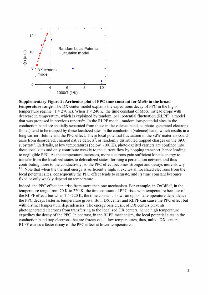
temperature range. The DX center model explains the expeditious decay of PPC in the high-temperature regime (T > 270 K). When T < 240 K, the time constant of MoS2 instead drops with decrease in temperature, which is explained by random local potential fluctuation (RLPF), a model that was proposed in previous reports1,2. In the RLPF model, random low-potential sites in the conduction band are spatially separated from those in the valence band, so photo-generated electrons (holes) tend to be trapped by these localized sites in the conduction (valence) band, which results in a long carrier lifetime and the PPC effect. These local potential fluctuation in the vdW materials could arise from disordered, charged native defects2, or randomly distributed trapped charges on the SiO2 substrate3. In details, at low temperatures (below ~100 K), photo-excited carriers are confined into these local sites and only contribute weakly to the current flow by hopping transport, hence leading to negligible PPC. As the temperature increases, more electrons gain sufficient kinetic energy to transfer from the localized states to delocalized states, forming a percolation network and thus contributing more to the conductivity, so the PPC effect becomes stronger and decays more slowly 1,4. Note that when the thermal energy is sufficiently high, it excites all localized electrons from the local potential sites, consequently the PPC effect tends to saturate, and its time constant becomes fixed or only weakly depend on temperature1. Indeed, the PPC effect can arise from more than one mechanism. For example, in ZnCdSe4, in the temperature range from 70 K to 220 K, the time constant of PPC rises with temperature because of the RLPF effect; but when T > 220 K, the time constant shows an opposite temperature dependence: the PPC decays faster as temperature grows. Both DX center and RLPF can cause the PPC effect but with distinct temperature dependencies. The energy barrier, Ec, of DX centers prevents photogenerated electrons from transferring to the localized DX centers, hence high temperature expedites the decay of the PPC. In contrast, in the RLPF mechanism, the local potential sites in the conduction band trap electrons that are frozen-out at low temperatures, thus, unlike DX centers, RLPF causes a faster decay of the PPC effect at lower temperatures.
4 6 8 106
8
10
12
ln(
) (a
.u.)
1000/T (1/K)
Random Local Potential Fluctuation model
DX centers model

3
Supplementary Figure 3: Temperature-dependent conductivity and photoconductivity. a, Arrhenius plots of dark electron density (n 𝐺 × 𝑇𝛾) for MoS2 and Mo0.3W0.7S2 to determine binding energy Eb. b, Transient normalized-PPC curves at various temperatures for Mo0.3W0.7S2, where the time constant is extracted by fitting with the stretched-exponential equation and shown in Fig. 3b. We extract the thermal activation energy (Eb) for deep levels in MoS2 and Mo0.3W0.7S2 from the Arrhenius plot of the dark conductance versus inverse temperature as in Supplementary Fig. 3a. The carrier density (n) depends exponentially on temperature, 𝑛 ~ exp(−𝐸𝑏/𝑘𝐵𝑇), considering the Boltzmann distribution and the “full-slope” regime in the freeze-out curves of semiconductors, where only a small portion of the deep levels are ionized 5,6. On the other hand, conductivity can be expressed by the Drude model as 𝜎 = 𝑛 𝑒 𝜇, where 𝜇 is the mobility following a temperature dependence of 𝜇 ~ 𝑇−𝛾 above ~ 200 K as reported in previous studies7-9. Combining these equations, n is related to the conductance G and expressed as,
𝐺 × 𝑇𝛾 𝑛 exp (−𝐸𝑏
𝑘𝐵𝑇). (1)
Arrhenius plot of Supplementary Eq. (1) yields an activation energy of 0.12 eV for MoS2 by using an exponent of 𝛾 = 1.7 as reported in literature8. We also found that the obtained value of Eb is insensitive to the value of 𝛾 used in the fitting, and only changes from 0.09 to 0.13 eV when 𝛾 is changed from 0.5 to 2.5. Similarly, we extract the activation energy of 0.30eV for Mo0.3W0.7S2 in Supplementary Fig. 3a, where 𝛾 uses the interpolated value of 1.9 following the known values of 1.7 for MoS2 and 2.0 for WS2
8,9. These Eb values (0.12 eV for MoS2 and 0.3 eV for Mo0.3W0.7S2) are shallower than the energy level Ei for sulfur vacancy (VS) measured from ECB. Therefore, they must originate from a defect level other than the VS. As the only other deep level identified from DLTS is the DX centers, we assign the extracted Eb to the energy distance between ECB and the EDX. That is, Eb = ECB - EDX = Ee - Ec.
0 6000 12000 180000.0
0.2
0.4
0.6
0.8
1.0
No
rma
lize
d P
PC
(a
.u.)
Time (s)
240K 250K
270K 290K
310K 358K
Fit
Mo0.3W0.7S2
ba
2.5 3.0 3.5 4.0 4.5 5.06
8
10
12
Mo0.3W0.7S2
= 1.9, Eb = 0.30 eV
MoS2
= 1.7, Eb = 0.12 eV
ln(GT)
(a.u
.)
1000/T (1/K)
4
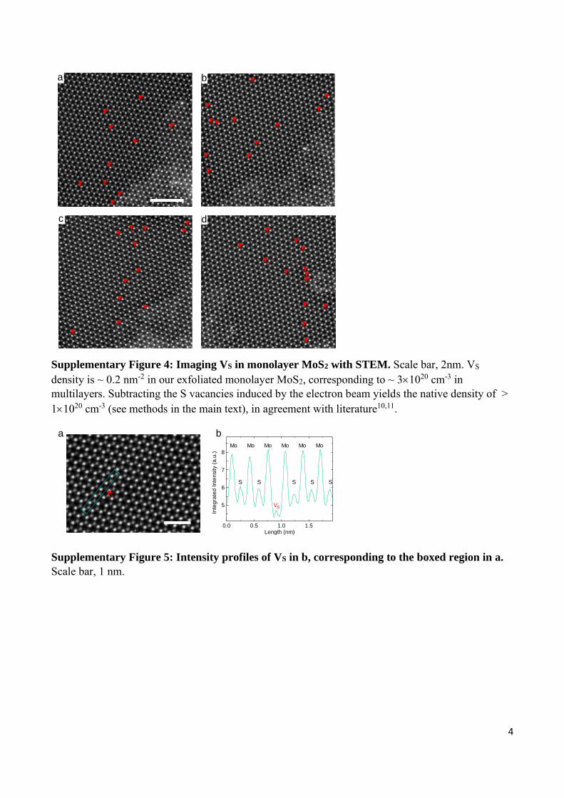
Supplementary Figure 4: Imaging VS in monolayer MoS2 with STEM. Scale bar, 2nm. VS density is ~ 0.2 nm-2 in our exfoliated monolayer MoS2, corresponding to ~ 31020 cm-3 in multilayers. Subtracting the S vacancies induced by the electron beam yields the native density of > 11020 cm-3 (see methods in the main text), in agreement with literature10,11.
Supplementary Figure 5: Intensity profiles of VS in b, corresponding to the boxed region in a.
Scale bar, 1 nm.
a b
c d
0.0 0.5 1.0 1.5
5
6
7
8
Inte
gra
ted
In
ten
sity (
a.u
.)
Length (nm)
Mo Mo Mo Mo Mo Mo
S S S S S
VS
a b

5
Supplementary Figure 6: Band bending of a n-type Schottky junction in response to the biased
voltage for deep donors in a, and partly passivated deep acceptors in b. Blue blocks represent passivated (hence inactive and always neutral) deep acceptors. Stage ① - ③ correspond to those in Fig. 1c.
The concentration of VS determined from STEM in Supplementary Fig. 4 is about 11020 cm-3 in MoS2, which is much higher than the free electron density of not intentionally doped MoS2 on the order of ~ 1018 cm-3 as reported in literature7,12.This could be attributed to either compensation or passivation of the deep levels, as widely observed and reported in many traditional semiconductors13-
15. Supplementary Figure 6a presents the band bending of deep donors with full occupancy in the ground state, akin to the schematic in the main text. However, deep traps in semiconductors may be passivated, and hence de-activated at equilibrium, as shown in the case of deep acceptors in Supplementary Fig. 6b, leading to only a small portion of traps in the depletion zone being active and able to emit electrons under the reverse bias. The mechanism of passivation of the deep levels is currently unknown in MoS2, and is beyond the scope of this study, but the small capture cross section of VS deep acceptors and their weak attraction to free electrons may play a role.
-
+
- - -
+ ECB
EVB
Ei
Electron emission
-
- - - --
qVR
EFn
+ ECB
EVB
Ei
- - - --
++EFm
+
deep traps
a
-
-
- - -
- -
ECB
EVB
Ei
Electron emission
-
-
- - - --
-
qVR
EFn
-
ECB
EVB
Ei
- - - --
EFm
-deep traps
Deep donors (0/+)
b Deep acceptors (0/-) with passivation

6
Supplementary Note 1: Calculation of deep level capture cross section from DLTS.
Rewriting Eq. (1) yields 𝑙𝑛 (𝑇2
𝑒𝑛) = 𝑙𝑛 (
1
𝐾∙𝜎𝑛) + (
𝐸𝐶𝐵−𝐸𝑖
𝑘)1000
𝑇, where the extrapolation in the Arrhenius
plot (Fig. 2b) allows extraction of the capture cross section, 𝜎𝑛. The constant K is expressed as5,16
𝐾 = 2(2𝜋𝑚𝑒
∗𝑘
ℎ2)3/2
(3𝑘
𝑚𝑡𝑐∗ )
1/2
= 3.26 × 10²¹ [1
𝑐𝑚2𝐾2𝑠] × (
𝑚𝑒∗3
𝑚𝑡𝑐∗ )
1/2
, (2)
where 𝑚𝑡𝑐∗ is the normalized thermal velocity effective mass, and 𝑚𝑒
∗ is the normalized density of states mass. The latter mass has been determined to be 0.50 (normalized to the free electron mass) as reported by previous studies17. The former mass is expressed as18
𝑚𝑡𝑐∗ =
4𝑚𝑙
[1+√𝑚𝑙/𝑚𝑡 sin−1(𝛿)/𝛿2]2 , (3)
where 𝛿 = √(𝑚𝑙 −𝑚𝑡)/𝑚𝑙, and 𝑚𝑙 and 𝑚𝑡 are the longitudinal and transverse effective masses in the ellipsoidal energy surface18. Our DFT calculation determines 𝑚𝑙 and 𝑚𝑡 to be 0.62 and 0.55, respectively, hence giving 𝑚𝑡𝑐
∗ = 0.57. Finally, the capture cross section of VS is calculated to be ~3.6×10⁻¹⁸ cm2 in MoS2.
7
Supplementary Note 2: Impact of our results: prediction of deep levels of anion impurities.
The knowledge of VS attained in this study can be used to understand and predict energy levels of anion-substitutional impurities such as oxygen in MoS2 or WS2. In order to explain this prediction, we start with discussing the bonding / antibonding model for a di-atomic system with the secular equation19,20
|𝐸 − 𝐸A0 𝑉
𝑉 𝐸 − 𝐸B0| = 0, (4)
where EA0 and EB0 (lower than EA0) are the atomic levels, and V is the interaction between EA0 and EB0 arising from the wavefunction overlap. Solving this equation yields two eigenvalues, corresponding to the molecular bonding and antibonding energy levels:
𝐸𝐴 =𝐸𝐴0+𝐸𝐵0
2+
1
2√(𝐸𝐴0 − 𝐸𝐵0)
2 + 4𝑉2, (5)
and
𝐸𝐵 =𝐸𝐴0+𝐸𝐵0
2−
1
2√(𝐸𝐴0 − 𝐸𝐵0)2 + 4𝑉2. (6)
Then rewriting of Supplementary Eq. (4) gives
∆′=1
2(√∆0
2 + 4𝑉2 − ∆0), (7)
where ∆0= 𝐸𝐴0 − 𝐸𝐵0 > 0 represents the energy difference between the initial atomic levels, and ∆′= 𝐸𝐴 − 𝐸𝐴0 > 0 is the difference in energy between the atomic level and its originated molecular orbital (Supplementary Fig. 7). In order to determine the evolution of Supplementary Eq. (7) with the change in ∆0, the first-order differentiation is calculated as
𝑑∆′
𝑑∆0=
1
2(
∆0
√∆02+4𝑉2
− 1) < 0, (8)
indicating a monotonically decreasing function of Supplementary Eq. (7). This suggests that increase in the difference of the initial atomic levels will reduce the splitting between the atomic and molecular levels (∆′, see Supplementary Fig. 7).

8
Supplementary Figure 7: Bonding / antibonding model explaining the formation of deep levels
in the bandgap of MoWS2. The left-hand side is schematic of the atomic levels of Mo(W) and S atoms and the resultant antibonding and bonding states in MoS2 (WS2). The right-hand side shows atomic level of the Mo(W) atom and substitutional O atom (defect) and the resultant deep and hyper-deep levels in MoS2 (WS2) with O defects. Next, we discuss the formation of the energy level induced by more electronegative, anion substitutional impurities in MoS2 or WS2 in Supplementary Fig. 7. The left-hand side presents the creation of conduction and valence bands in MoS2 following the simplest possible bonding / antibonding model. We note that, according to the origins of conduction band maximum (CBM) and the valence band minimum (VBM) in MoS2 or WS2
21, the antibonding state (ECB) in Supplementary Fig. 7 can be defined as the CBM, while the bonding state (EVB) is deeper than the VBM, so the difference between ECB and EVB is not equal to the bandgap. The energy difference between the atomic level of Mo(W) atom and the formed conduction band of Mo(W)S2, ∆′(S), can be expressed by Supplementary Eq. (7). As calculated by DFT in Fig. 2d, the wavefunction of VS is composed mainly of orbitals of Mo(W) atoms, hence it is reasonable to assume that the position of VS level lies very close to the atomic level of Mo(W), EMo(W), in Supplementary Fig. 7. Considering anion impurities such as oxygen substituting S in MoWS2, the interaction between the O atom and its neighboring Mo(W) atoms forms two molecular levels, a deep level and a so-called hyper-deep level22. The latter is below the valence band and electrically inactive; in contrast, the former lies inside the bandgap and its wavefunctions is dominated by that of Mo(W), so it is called host-like defect level as shown in the right-hand side of Supplementary Fig. 7, akin to the nitrogen defect in GaP22,23.
The low-lying oxygen atomic level with respect to the vacuum level means a more significant difference in the original energies (∆0(O) = 𝐸𝑀𝑜 − 𝐸𝑂) than that in host materials (∆0(S) = 𝐸𝑀𝑜 −
𝐸𝑆), resulting in the smaller splitting ∆′(O) in Supplementary Fig. 7, following the Supplementary Eq. (7) and (8). Due to the high electronegativity of O atom, the Mo(W)-O can form a more ionic bond with weaker wavefunction overlap and hence a smaller value of V (Supplementary Eq. (7)),
EMo(W)
ES
Antibonding (ECB)
Bonding (EVB)
EMo(W)
EO
Deep level
(host like)
Hyper-deep level
(impurity like)
Atom
orbital
Molecular
orbital
Molecular
orbital
Atom
orbital
Host Defect
VS
∆
∆
∆0
∆0
9
compared to the more covalent Mo(W)-S bond. In summary, it is reasonable to predict that anion impurities would create deep levels with similar energies as the VS, about 0.3 eV below the CBM, in Mo1-xWxS2 of all compositions.
Finally, the analysis above is not limited to Mo(W) disulfides; all other transition metal chalcogenides may be similarly discussed in the context of native defect energies once the anion vacancy level is measured.
10
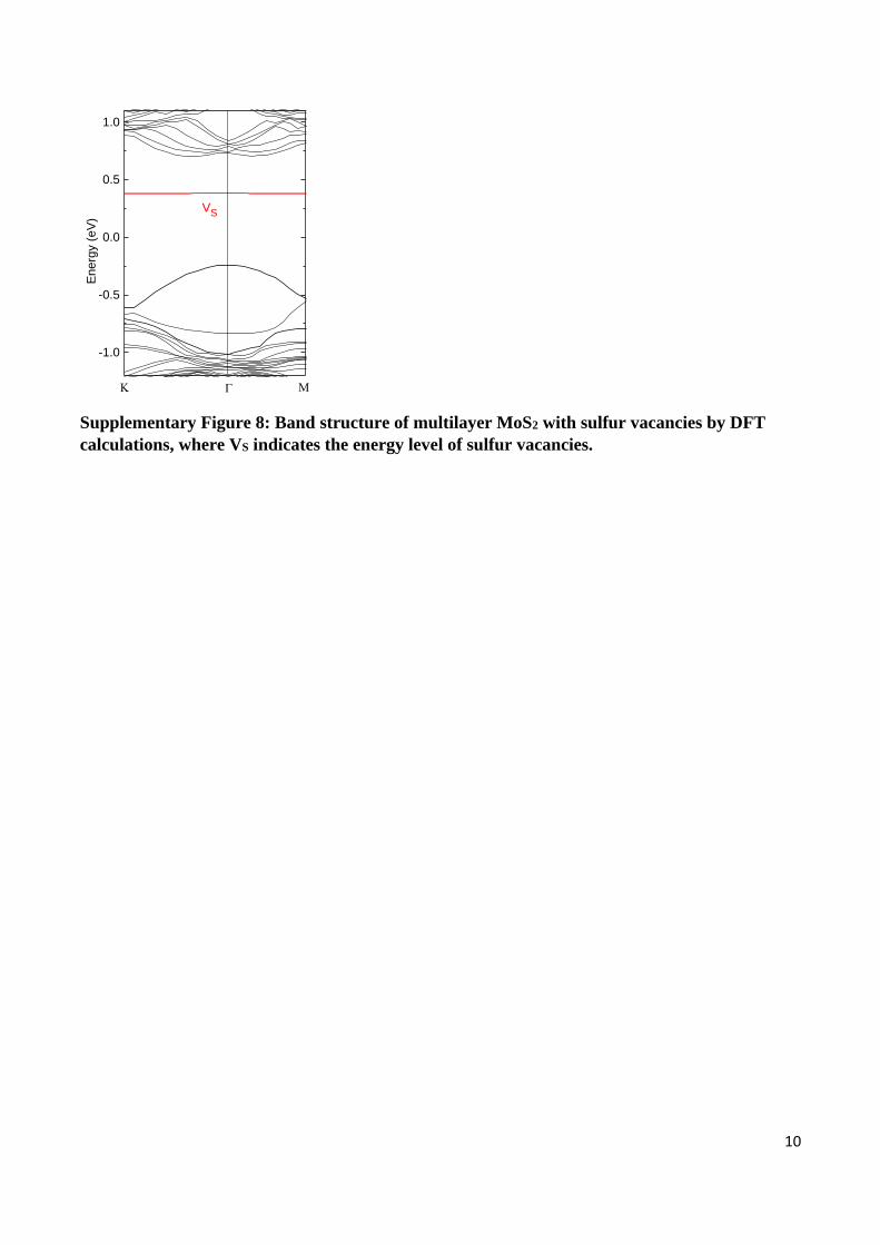
Supplementary Figure 8: Band structure of multilayer MoS2 with sulfur vacancies by DFT
calculations, where VS indicates the energy level of sulfur vacancies.
-1.0
-0.5
0.0
0.5
1.0
En
erg
y (
eV
)
VS
b

11
Supplementary Note 3: Characterization of vdW crystals Field-effect transistors.
Supplementary Figure 9: Source-drain current (IDS) in response to the gate voltage (VGate) of
field-effect transistors (FET) made of WS2 at room temperature.
It is known that undoped MoS2 has a native electron density over orders of magnitude higher than in WS2
24,25. Here we explain it using the chemical trend of DX centers in these materials.
According to the data in Fig. 5b, we can extract the low-field field-effect mobility to be ~ 16 cm2/(V∙S) for MoS2. Thus, the free carrier density (𝑛 = 1/(𝑒 ∙ 𝜇 ∙ 𝜌)) of MoS2 is calculated to be ~ 4×1017 cm-3, consistent with results in previous studies12,24. Similarly, the free electron concentration of WS2 is determined to be 7×1013 cm-3 by the FET results in Supplementary Fig. 9, also in good agreement with literature25.
Next, we discuss the effect of DX centers on the free carrier density in MoS2 and WS2. We assume the native donor density is on the same level in these two materials, but they are compensated to different extents by the DX centers as deep traps, because of their different energy depths in the bandgap of the hosts. Supplementary Equation 1 is then used to estimate the carrier density ratio of MoS2 to WS2
𝑛(𝑀𝑜𝑆2)
𝑛(𝑊𝑆2)= 𝑒𝑥𝑝 (
𝐸𝑏(𝑊𝑆2)−𝐸𝑏(𝑀𝑜𝑆2)
𝑘𝐵𝑇), (9)
where 𝐸𝑏(𝑀𝑜 2) = 0.12 eV is the energy depth of DX centers in MoS2, 𝐸𝑏(𝑊 2) can be found by extrapolation to be ~ 0.38 eV based on the value of MoS2 and Mo0.3W0.7S2 in Fig.4c, and 𝑘𝐵𝑇 = 26 meV at room temperature. Therefore, we obtain free carrier density ratio (𝑛(𝑀𝑜 2)/𝑛(𝑊 2)) to be ~ 2×10⁴ due to the charge compensation by DX centers. This is on the same order of magnitude as the value (5×10³) determined from FET measurements.
-10 -5 0 5 10
0
200
400
600
I DS
(n
A)
VGate
(V)
WS2
12
Supplementary Note 4: Stray capacitance analysis and capacitance-voltage characterization.
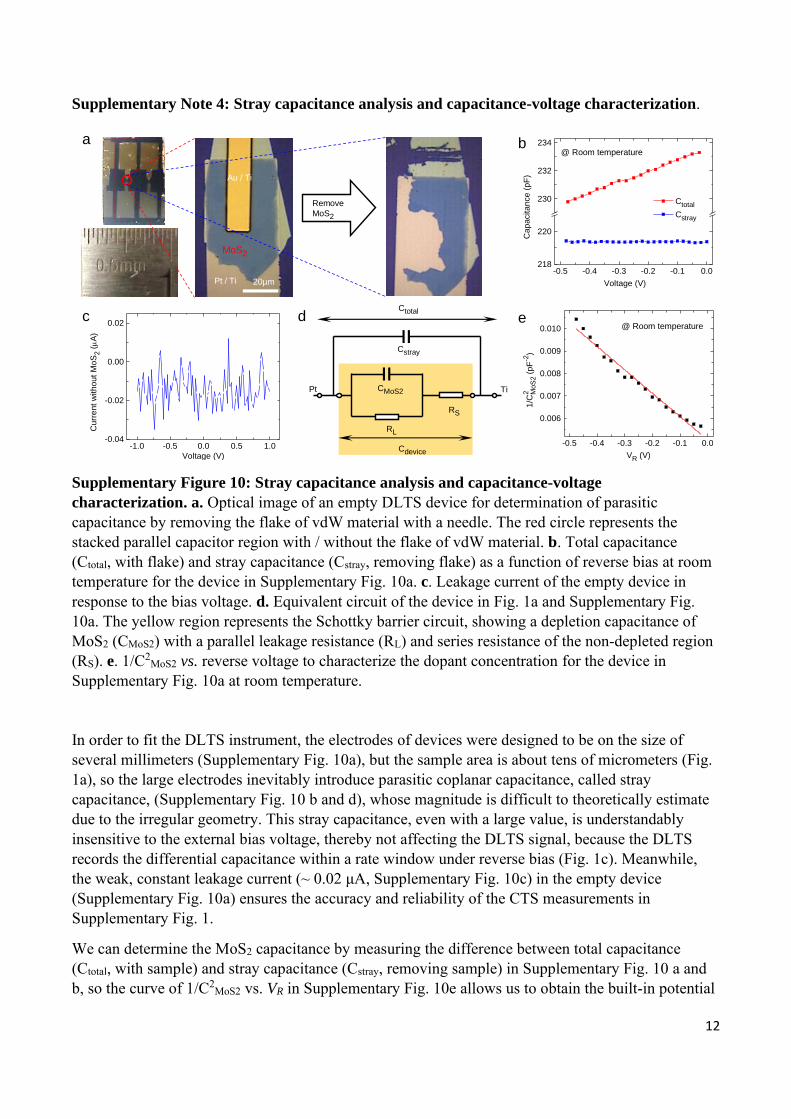
Supplementary Figure 10: Stray capacitance analysis and capacitance-voltage
characterization. a. Optical image of an empty DLTS device for determination of parasitic capacitance by removing the flake of vdW material with a needle. The red circle represents the stacked parallel capacitor region with / without the flake of vdW material. b. Total capacitance (Ctotal, with flake) and stray capacitance (Cstray, removing flake) as a function of reverse bias at room temperature for the device in Supplementary Fig. 10a. c. Leakage current of the empty device in response to the bias voltage. d. Equivalent circuit of the device in Fig. 1a and Supplementary Fig. 10a. The yellow region represents the Schottky barrier circuit, showing a depletion capacitance of MoS2 (CMoS2) with a parallel leakage resistance (RL) and series resistance of the non-depleted region (RS). e. 1/C2
MoS2 vs. reverse voltage to characterize the dopant concentration for the device in Supplementary Fig. 10a at room temperature.
In order to fit the DLTS instrument, the electrodes of devices were designed to be on the size of several millimeters (Supplementary Fig. 10a), but the sample area is about tens of micrometers (Fig. 1a), so the large electrodes inevitably introduce parasitic coplanar capacitance, called stray capacitance, (Supplementary Fig. 10 b and d), whose magnitude is difficult to theoretically estimate due to the irregular geometry. This stray capacitance, even with a large value, is understandably insensitive to the external bias voltage, thereby not affecting the DLTS signal, because the DLTS records the differential capacitance within a rate window under reverse bias (Fig. 1c). Meanwhile, the weak, constant leakage current (~ 0.02 μA, Supplementary Fig. 10c) in the empty device (Supplementary Fig. 10a) ensures the accuracy and reliability of the CTS measurements in Supplementary Fig. 1.
We can determine the MoS2 capacitance by measuring the difference between total capacitance (Ctotal, with sample) and stray capacitance (Cstray, removing sample) in Supplementary Fig. 10 a and b, so the curve of 1/C2
MoS2 vs. VR in Supplementary Fig. 10e allows us to obtain the built-in potential
-1.0 -0.5 0.0 0.5 1.0-0.04
-0.02
0.00
0.02
Curr
en
t w
ith
ou
t M
oS
2 (
A)
Voltage (V)
a b
c d
RL
CMoS2Pt Ti
RS
Cstray
Ctotal
Cdevice
e
-0.5 -0.4 -0.3 -0.2 -0.1 0.0
0.006
0.007
0.008
0.009
0.010 @ Room temperature
1/C
2 MoS
2 (
pF
-2)
VR (V)
-0.5 -0.4 -0.3 -0.2 -0.1 0.0218
220
230
232
234
Ctotal
Cstray
Cap
acita
nce
(p
F)
Voltage (V)
@ Room temperature
Au / Ti
Pt / Ti
MoS2
20µm
Remove
MoS2

13
(Φbi) of ~ 0.5 V for MoS2/Pt Schottky diode and the dopant concentration of ~ 3×1018 cm-3 in nominally not intentionally doped MoS2 (Nd) at room temperature, via its intercept and the slope according to26
1
𝐶𝑀𝑜𝑆22 =
2(|Φ𝑏𝑖|+|𝑉𝑅|)
𝑞𝑁𝑑 𝑟 0𝐴2, (10)
where 휀𝑟 = 11 is the dielectric constant of multilayer MoS227, 𝑉𝑅 is the reverse biased voltage (Fig.
1c), A is the area of the depletion zone, and CMoS2 is close to Cdevice (= Ctotal - Cstray). These two extracted parameters for MoS2 are consistent with previous results in literature7,12,28. As a result, the depletion width of the Schottky junction can be expressed as26
𝑊 = √2 𝑟 0(|Φ𝑏𝑖|+|𝑉𝑅|)
𝑞𝑁𝑑, (11)
and estimated to be ~ 22 nm under the reverse bias of 0.5 V at room temperature. Note that the dopant concentration determined here is significantly higher than the free electron density measured by FET in Supplementary Fig. 9, which is attributed to the trapping of free electrons by DX centers.
The linear 1/C2 vs. VR curve indicates a roughly uniform distribution of dopants and nearly step junction profile of space charge density near the surface of the MoS2/Pt Schottky diode16,29, hence confirming the feasibility of Supplementary Eq. (11) to extract the depletion width.
Although it is reasonable to assume a nearly step junction profile for the space charge, in reality the free carrier density varies exponentially within the depletion zone, so a Debye screening length (or Debye tail, Debye incursion) is defined to express the abruptness of the space charge distribution near the edge of the depletion zone, which can be written as16
𝐿𝐷 = √ 𝑟 0𝑘𝑇
𝑞2𝑁𝑑. (12)
In our case, the high dopant concentration (Nd ~ 3×1018 cm-3) yields a Debye length of ~ 2 nm at room temperature, which is on the same order with that in heavily doped silicon16. The depletion width (~22 nm) is more than ten times greater than this Debye length, which in turn justifies the sharp, nearly step - function profile of space charge16.
In the above description, we assume that CMoS2 is almost equal to Cdevice by omitting the effect of the leakage resistance (RL) and the series resistance (RS). When subtracting the parallel stray capacitance, the measured capacitance, Cdevice in the circuit within the yellow shadow (Supplementary Fig. 10d), is related to CMoS2 by16
𝐶𝑀𝑜𝑆2
𝐶𝑑𝑒𝑣𝑖𝑐𝑒= (1 +
𝑅𝑆
𝑅𝐿)2
+ (𝑅𝑆
1 𝜔𝐶𝑀𝑜𝑆2⁄)2
, (13)
where 𝜔 is the frequency of a.c. voltage during the capacitance measurement and is 1 MHz in our case. Accurate test of the depletion capacitance and hence the depletion width requires that RS << RL and RS << 1/ωCMoS2, such that the capacitive impedance, CMoS2, dominates the circuit element16,29,30. The leakage resistance (RL) and series resistance (RS) can be approximately estimated from the reverse and forward bias current of the Schottky junction to be 80 kΩ and 2.5 kΩ under the reverse bias of 0.2V at 320 K (Fig. 1e), meeting the requirement of RS << RL. Given that CMoS2 ≈ Ctotal – Cstray, 1/ωCMoS2 = 77 kΩ >> RS at 320 K. Therefore, Supplementary Equation (13) gives CMoS2 ~ Cdevice, which justifies the reliability of the capacitance measurements. We note that the large leakage
14
current under reverse bias, called ‘soft’ reverse characteristics, may be attributed to the tunneling effect or the lowering of Schottky barrier height by image forces, as commonly reported in the Schottky junctions formed by low dimensional materials31-33.
15
Supplementary Note 5: Thermodynamic interpretation of Arrhenius plots in DLTS.
The defect energy level in semiconductors is defined as the change of chemical potential due to the formation of a pair of charged carrier and ionized defect34,35. The chemical potential thermodynamically means the variation of Gibbs free energy during the capture or emission of an electron at constant pressure and temperature. Thus, based on these definitions, the Arrhenius equation of the thermal emission rate in Eq. (1) can be rewritten as35 𝑒𝑛
𝑇2 = 𝐾𝜎𝑛 exp (−
ΔG(𝑇)
𝑘𝐵𝑇), (14)
where ΔG(𝑇) = |𝐸𝐶𝐵 − 𝐸𝑖| and is the activation energy for electron emission from the deep state to the conduction band edge. At the same time, the Gibbs free energy is defined by the thermodynamic identity as ΔG(𝑇) = ΔH − TΔS, where ΔH and ΔS represent the changes in enthalpy and entropy, respectively. Therefore, Supplementary Equation (14) becomes16 𝑒𝑛
𝑇2 = 𝐾[exp (ΔS
𝑘𝐵) 𝜎𝑛] exp (−
ΔH
𝑘𝐵𝑇), (15)
and hence the slope of the Arrhenius plot via Eq. (1) yields an average of enthalpy change over the temperature range of this plot, considering the generally weak temperature dependence of ΔH16. The difference between ΔG and ΔH mainly arises from the lattice vibrational contribution to ΔS due to the coupling of occupied deep states to the lattice, and therefore, it is usually negligible when electrons are excited from the traps to conduction band without changing the bonding configuration (ΔS ~ 0)36. Thus, in this study, it is reasonable to consider the measured Arrhenius slope from DLTS as the activation energy for VS states, because our DFT calculations do not observe lattice relaxation or entropy change during the transfer of electrons between the VS defect and the conduction band edge.
With regard to DX centers, most of previous studies on group III-V semiconductors also neglected the difference between ΔG and ΔH37-43, despite the occurrence of lattice relaxation when a DX center switches to the electron-donating state. In this study, we do not consider this difference for DX centers in vdW crystals. On the other hand, in order to obtain the exact activation energy, ΔG(T), via Supplementary Eq. (14), one needs to measure the values of both 𝑒𝑛 and 𝜎𝑛 at desired temperatures. The emission rate, 𝑒𝑛, can be determined by the DLTS or transient capacitance test, while the capture cross section is usually measured using the diode short-circuiting technique44,45, which is out of the scope of this study.
The main text and Supplementary Note 1 show the extraction of capture cross section, 𝜎𝑛, of VS deep state via the intercept of the Arrhenius plot in Fig. 2b. However, we note that, based on Supplementary Eq. (15), this intercept more accurately represents the product exp (ΔS
𝑘𝐵) 𝜎𝑛, rather
than just 𝜎𝑛. Experimentally, one could measure the latter using the diode shorting-circuiting technique44,45to eventually determine the prefactor, ΔS, by temperature-dependent Gibbs free energy (ΔG = ΔH - TΔS).

16
Supplementary Note 6: Activation energy of DX centers by Arrhenius plot of DLTS.
Unlike regular deep levels which have no capture/emission barriers, such as the VS state, for DX centers the Arrhenius plot of the DLTS spectrum extracts the emission barrier Ee, which is not the energy of the DX center directly measured from the conduction or valence band edges. This is because, in the case of DX centers, the energy barrier, Ec in the configurational coordinate diagram (CCD, Fig. 3c and 4c), must be overcome in order for an electron to be trapped by defects, hence leading to a strongly temperature-dependent capture cross section5,
𝜎𝑛,𝐷𝑋 = 𝜎∞ exp (− 𝐸𝑐𝑘𝐵𝑇
). (16)
Combining Supplementary Eq. (16) and Eq. (1) gives 𝑒𝑛
𝑇2 = 𝐾𝜎∞ exp (−|𝐸𝐶𝐵−𝐸𝑖|+𝐸𝑐
𝑘𝐵𝑇), (17)
where |𝐸𝐶𝐵 − 𝐸𝑖| + 𝐸𝑐 is equal to the emission energy, Ee, in the CCD (Fig. 3c) without considering the entropy change, and Ei is EDX.
To sum up, the DLTS spectrum measures the activation energy or binding energy (Eb) for normal defects such as the VS states, while for DX centers, DLTS yields the emission energy (Ee), the summation of binding energy (Eb) and capture barrier (Ec).
17
Supplementary Note 7: Excluding a surface depletion mechanism for the PPC effect.
Although a surface depletion model was used to explain PPC effects in some low-dimensional systems46,47, this model is unlikely to explain our observed PPC in MoS2 and alloys. This is because PPC effects induced by surface depletion, for instance, in Si NWs or α-In2Se3 nanosheets46,47, originate from self-assembled molecules on the surface or oxygen ions adsorbed from the environment. However, our STEM images (Fig. 1b) confirm the absence of adsorbents or contamination on the surface. Moreover, all the PPC tests were completed in high vacuum (~ 10-6 torr) after annealing at 400 K in vacuum for at least one day to remove possible adsorbents. In the meantime, such surface depletion mechanism usually induces only a weak PPC with a short decay constant (e.g., ~ seconds at room temperature)46, in stark contrast to the long PPC decay time we observed (~ 105 s for multilayer MoS2 at room temperature). Therefore, our PPC effect observed in MoS2 and alloys is unlikely to be caused by any surface modification of the samples.
18
Supplementary References
1 Jiang, H. & Lin, J. Percolation transition of persistent photoconductivity in II-VI mixed crystals. Physical review letters 64, 2547 (1990).
2 Wu, Y.-C. et al. Extrinsic origin of persistent photoconductivity in monolayer MoS 2 field effect transistors. Scientific reports 5, 11472 (2015).
3 Xue, J. et al. Scanning tunnelling microscopy and spectroscopy of ultra-flat graphene on hexagonal boron nitride. Nature materials 10, 282-285 (2011).
4 Jiang, H. & Lin, J. Persistent photoconductivity and related critical phenomena in Zn 0.3 Cd 0.7 Se. Physical Review B 40, 10025 (1989).
5 McCluskey, M. D. & Haller, E. E. Dopants and defects in semiconductors. (CRC press, 2018). 6 Chand, N. et al. Comprehensive analysis of Si-doped Al x Ga 1− x As (x= 0 to 1): Theory and experiments.
Physical Review B 30, 4481 (1984). 7 Radisavljevic, B. & Kis, A. Mobility engineering and a metal–insulator transition in monolayer MoS 2.
Nature materials 12, 815-820 (2013). 8 Perera, M. M. et al. Improved carrier mobility in few-layer MoS2 field-effect transistors with ionic-
liquid gating. ACS nano 7, 4449-4458 (2013). 9 Xu, S. et al. Universal low-temperature Ohmic contacts for quantum transport in transition metal
dichalcogenides. 2D Materials 3, 021007 (2016). 10 Hong, J. et al. Exploring atomic defects in molybdenum disulphide monolayers. Nature
communications 6, 1-8 (2015). 11 Qiu, H. et al. Hopping transport through defect-induced localized states in molybdenum disulphide.
Nature communications 4, 1-6 (2013). 12 Radisavljevic, B., Radenovic, A., Brivio, J., Giacometti, V. & Kis, A. Single-layer MoS 2 transistors. Nature
nanotechnology 6, 147 (2011). 13 Lagowski, J., Kaminska, M., Parsey Jr, J., Gatos, H. & Lichtensteiger, M. Passivation of the dominant
deep level (EL2) in GaAs by hydrogen. Applied Physics Letters 41, 1078-1080 (1982).
14 Dautremont‐Smith, W. et al. Passivation of deep level defects in molecular beam epitaxial GaAs by hydrogen plasma exposure. Applied physics letters 49, 1098-1100 (1986).
15 Nabity, J. et al. Passivation of Si donors and DX centers in AlGaAs by hydrogen plasma exposure. Applied physics letters 50, 921-923 (1987).
16 Blood, P. & Orton, J. W. The electrical characterization of semiconductors: majority carriers and electron states. Vol. 2 (Academic press London, 1992).
17 Peelaers, H. & Van de Walle, C. G. Effects of strain on band structure and effective masses in MoS 2. Physical Review B 86, 241401 (2012).
18 Green, M. A. Intrinsic concentration, effective densities of states, and effective mass in silicon. Journal of Applied Physics 67, 2944-2954 (1990).
19 Ci, P. et al. Quantifying van der Waals interactions in layered transition metal dichalcogenides from pressure-enhanced valence band splitting. Nano letters 17, 4982-4988 (2017).
20 Burns, G. Solid State Physics. (Elsevier Science, 1985). 21 Kang, J., Tongay, S., Zhou, J., Li, J. & Wu, J. Band offsets and heterostructures of two-dimensional
semiconductors. Applied Physics Letters 102, 012111 (2013). 22 Hjalmarson, H. P., Vogl, P., Wolford, D. J. & Dow, J. D. Theory of substitutional deep traps in covalent
semiconductors. Physical Review Letters 44, 810 (1980). 23 Yu, P. Y. & Cardona, M. Fundamentals of semiconductors: physics and materials properties. (Springer,
1996). 24 Kwak, J. Y. et al. Electrical characteristics of multilayer MoS2 FET’s with MoS2/graphene
heterojunction contacts. Nano letters 14, 4511-4516 (2014). 25 Braga, D., Gutierrez Lezama, I., Berger, H. & Morpurgo, A. F. Quantitative determination of the band
gap of WS2 with ambipolar ionic liquid-gated transistors. Nano letters 12, 5218-5223 (2012). 26 Hu, C. Modern semiconductor devices for integrated circuits. Vol. 2 (Prentice Hall Upper Saddle River,
19
New Jersey, 2010). 27 Chen, X. et al. Probing the electron states and metal-insulator transition mechanisms in molybdenum
disulphide vertical heterostructures. Nature communications 6, 6088 (2015). 28 Kim, G.-S. et al. Schottky barrier height engineering for electrical contacts of multilayered MoS2
transistors with reduction of metal-induced gap states. ACS nano 12, 6292-6300 (2018). 29 Pierret, R. F. Semiconductor device fundamentals. (Pearson Education India, 1996). 30 Goodman, A. M. Metal—Semiconductor barrier height measurement by the differential capacitance
method—One carrier system. Journal of Applied Physics 34, 329-338 (1963). 31 Kumar, S. et al. Influence of barrier inhomogeneities on transport properties of Pt/MoS2 Schottky
barrier junction. Journal of Alloys and Compounds 797, 582-588 (2019). 32 Rhoderick, E. H. & Rhoderick, E. Metal-semiconductor contacts. (Clarendon Press Oxford, 1978). 33 Chen, C.-C., Aykol, M., Chang, C.-C., Levi, A. & Cronin, S. B. Graphene-silicon Schottky diodes. Nano
letters 11, 1863-1867 (2011). 34 Van Vechten, J. & Thurmond, C. Entropy of ionization and temperature variation of ionization levels
of defects in semiconductors. Physical Review B 14, 3539 (1976). 35 Thurmond, C. The standard thermodynamic functions for the formation of electrons and holes in Ge,
Si, GaAs, and GaP. Journal of the Electrochemical Society 122, 1133 (1975). 36 Almbladh, C.-O. & Rees, G. Statistical mechanics of electronic energy levels in semiconductors. Solid
State Communications 41, 173-176 (1982). 37 Criado, J., Gomez, A., Munoz, E. & Calleja, E. Deep level transient spectroscopy signature analysis of
DX centers in AlGaAs and GaAsP. Applied physics letters 49, 1790-1792 (1986).
38 Calleja, E., Gomez, A., Munoz, E. & Camara, P. Fine structure of the alloy‐broadened thermal emission spectra from DX centers in GaAlAs. Applied physics letters 52, 1877-1879 (1988).
39 Kasu, M., Fujita, S. & Sasaki, A. Observation and characterization of deep donor centers (DX centers)
in Si‐doped AlAs. Journal of applied physics 66, 3042-3046 (1989).
40 Calleja, E., Gomez, A. & Munoz, E. Direct evidence of the DX center link to the L‐conduction‐band minimum in GaAlAs. Applied physics letters 52, 383-385 (1988).
41 Mooney, P., Theis, T. & Wright, S. Effect of local alloy disorder on emission kinetics of deep donors (DX centers) in Al x Ga1− x As of low Al content. Applied physics letters 53, 2546-2548 (1988).
42 Kumagai, O., Kawai, H., Mori, Y. & Kaneko, K. Chemical trends in the activation energies of DX centers. Applied physics letters 45, 1322-1323 (1984).
43 Theis, T., Mooney, P. & Wright, S. Electron Localization by a Metastable Donor Level in n− GaAs: A New Mechanism Limiting the Free-Carrier Density. Physical review letters 60, 361 (1988).
44 Brotherton, S. & Lowther, J. Electron and hole capture at Au and Pt centers in silicon. Physical Review Letters 44, 606 (1980).
45 Brotherton, S. & Bicknell, J. The electron capture cross section and energy level of the gold acceptor center in silicon. Journal of Applied Physics 49, 667-671 (1978).
46 Anandan, M. et al. High-responsivity broad-band sensing and photoconduction mechanism in direct-Gap α-In2Se3 nanosheet photodetectors. Nanotechnology 31, 465201 (2020).
47 Zhao, X., Tu, P., He, J., Zhu, H. & Dan, Y. Cryogenically probing the surface trap states of single nanowires passivated with self-assembled molecular monolayers. Nanoscale 10, 82-86 (2018).