Embed Size (px)
Citation preview
nanomaterials
Article
Optically-Thin BroadbandGraphene-Membrane Photodetector
Tania Moein 1,2,*,†, Darius Gailevicius 3,*,† , Tomas Katkus 1,2, Soon Hock Ng 1,2 ,Stefan Lundgaard 1,2 , David J. Moss 1, Hamza Kurt 4, Vygantas Mizeikis 5,Kestutis Staliunas 6,7 , Mangirdas Malinauskas 3,8 and Saulius Juodkazis 1,2,8
1 Optical Sciences Centre, Swinburne University of Technology, John St., Hawthorn, VIC 3122, Australia;[email protected] (T.K.); [email protected] (S.H.N.); [email protected] (S.L.);[email protected] (D.J.M.); [email protected] (S.J.)
2 The ARC Training Centre in Surface Engineering for Advanced Materials (SEAM), School of Science,Swinburne University of Technology, Hawthorn, VIC 3122, Australia
3 Laser Research Center, Faculty of Physics, Vilnius University, Sauletekio Ave. 10, LT-10223 Vilnius, Lithuania;[email protected]
4 Department of Electrical and Electronics Engineering, TOBB University of Economics and Technology,Ankara 06560, Turkey; [email protected]
5 Research Institute of Electronics, Shizuoka University, 3-5-1 Johoku, Naka-ku, Hamamatsu 432-8561, Japan;[email protected]
6 Dep. de Física, Universitat Politècnica de Catalunya (UPC), Colom 11, E-08222 Terrassa, Spain;[email protected]
7 Institució Catalana de Recerca i Estudis Avançats (ICREA), Passeig Lluís Companys 23,E-08010 Barcelona, Spain
8 Tokyo Tech World Research Hub Initiative (WRHI), School of Materials and Chemical Technology,Tokyo Institute of Technology, 2-12-1, Ookayama, Meguro-ku, Tokyo 152-8550, Japan
* Correspondence: [email protected] (T.M.); [email protected] (D.G.)† T.M. and D.G. contributed equally.
Received: 20 December 2019; Accepted: 18 February 2020; Published: 25 February 2020
Abstract: A broadband graphene-on-Si3N4-membrane photodetector for the visible-IR spectralrange is realised by simple lithography and deposition techniques. Photo-current is producedupon illumination due to presence of the build-in potential between dissimilar metal electrodeson graphene as a result of charge transfer. The sensitivity of the photo-detector is ∼1.1 µA/W whenirradiated with 515 and 1030 nm wavelengths; a smaller separation between the metal contacts favorsgradient formation of the built-in electric field and increases the efficiency of charge separation.This optically-thin graphene-on-membrane photodetector and its interdigitated counterpart has thepotential to be used within 3D optical elements, such as photonic crystals, sensors, and wearableelectronics applications where there is a need to minimise optical losses introduced by the detector.
Keywords: optically thin photodetector; graphene; Si3N4 membrane; thermopower
1. Introduction
Graphene—a two dimensional (2D) crystal—has become the subject of intense research for avariety of applications including optoelectronics due to its exceptional electronic [1–3], optical, physicaland chemical properties [4–6]. Among the latest innovations, graphene has shown great potential innovel photonic devices such as photodetectors [1–4,6–11].
Despite the fact that graphene is a gapless material, it demonstrates strong interband absorptionfrom a broad range of wavelengths between visible and near-infrared (near-IR). Graphene for use in
Nanomaterials 2020, 10, 407; doi:10.3390/nano10030407 www.mdpi.com/journal/nanomaterials
Nanomaterials 2020, 10, 407 2 of 9
photodetectors rely on one or more photo current generation principles. These are: photo-conductive,photo-thermoelectric (via Seebeck effect), and bolometric photo-voltage generation [4,12–15].
To decrease the response time of bolometric photodetectors, the use of materials/structures witha low thermal capacitance is required. Silicon nitride Si3N4 membranes are good candidates due totheir low mass and excellent optical properties [16–18].
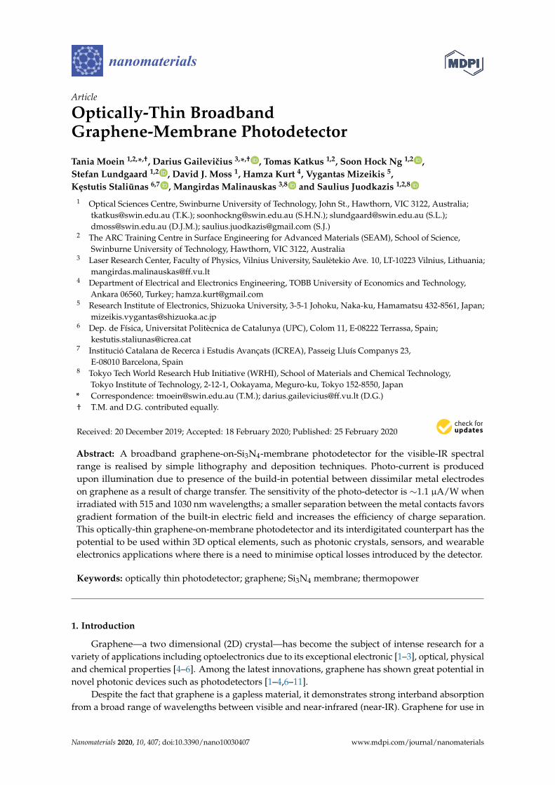
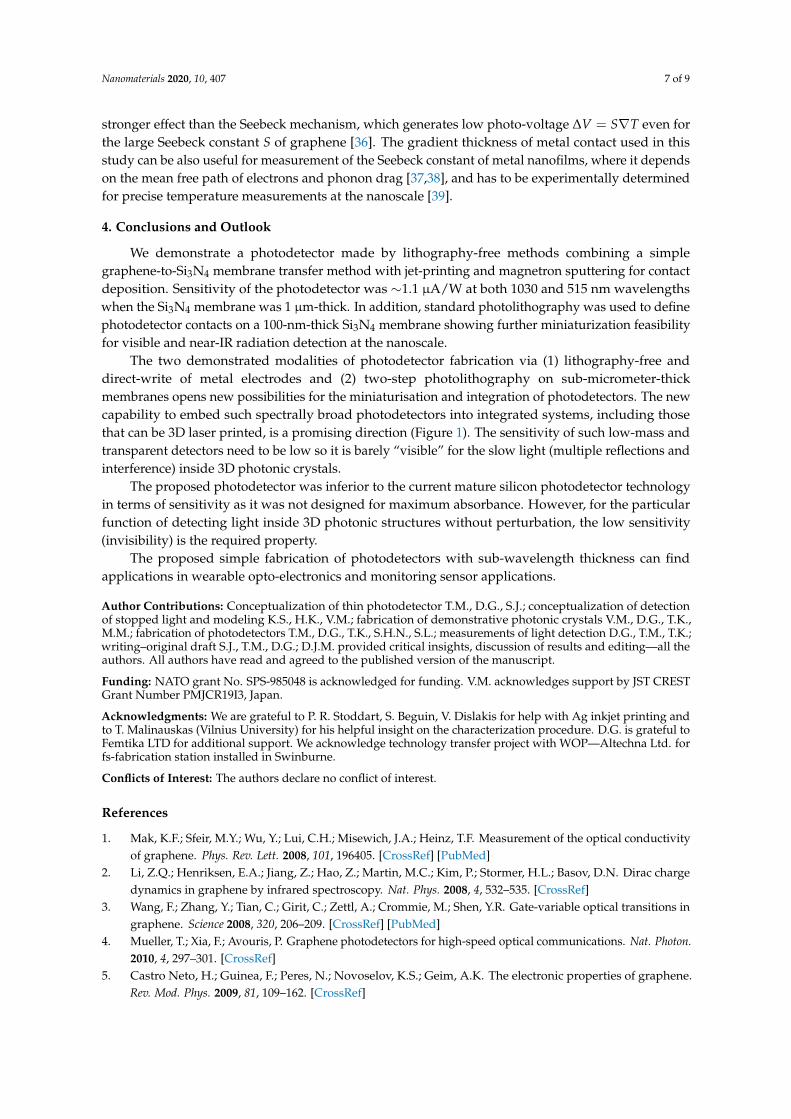
Motivation for this study is based on the current lack of photodetectors with small geometricalfootprints which can be integrated into micro-/nano-resonant structures used in optical sensors [19].In some applications, an ideal photodetector is a device that allows probing/monitoring light intensitywithout perturbing complex 3D photonic circuitry, e.g., slow light inside photonic crystals. Detectionof slow light localization inside a 3D woodpile photonic crystal in the visible-IR range is shown inFigure 1 [20,21]. The E-field distribution of light in these structures can be calculated and examinedindirectly, however, there are no tools to probe the field internally. Ideally, an optically thin detectorhas to be integrated inside 3D photonic lattices, e.g., made by state-of-the-art direct laser writing3D nanolithography [22,23]. A photodetector which is weakly absorbing and has low dispersion(non-pertubing 3D photonic crystal) could be made using a graphene-on-membrane approach.Such thin sensors are currently not available and can become practical via cost effective manufacturingas explored in this study. Applications for such graphene photodetectors include flexible and wearableelectronics, as well as applications where integration of multiple readout points for data analysis arerequired [24].
Here, we demonstrate a graphene-on-membrane photodetector using a micrometer thin Si3N4
membrane. Two different metals (Ag, Pd) are utilised as electrodes to create a build-in electricfield across the graphene [12], between the electrodes. The bias due to charge carrier doping atthe graphene-metal interface occurs as a result of differences in electron work function.
Slow light
10µm
Slow light
10 µm
(a) (b) (c)
Chirped Photonic Crystal
Photo-detector:
Photo-detector
Figure 1. Photodetector concept for slow light monitoring inside a photonic crystal [19]. (a) Schematicsof a graphene-based spectrally broadband photodetector for optical readout from within a spatiallychirped photonic crystal. The photodetector has to be optically thin and non-perturbing to thelocalisation of slow light and consists of a nanomembrane of Si3N4, electrodes, and a graphenelayer over the top (or below the contacts). (b) Side-view of the photodetector embedded inside thephotonic crystal and modeling of light intensity inside photonic crystal at the slow light mode. It showsspatial localisation of the Ez field component in the plane of the photodetector (calculations werecarried without a simulated detector) [25,26]. (c) Electron-microscope image of photonic crystal with aspatial chirp (vertical) polymerised out of a negative-tone SZ2080 resist.
2. Experimental: Samples and Procedures
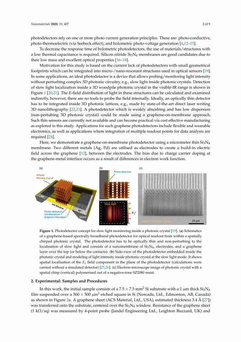
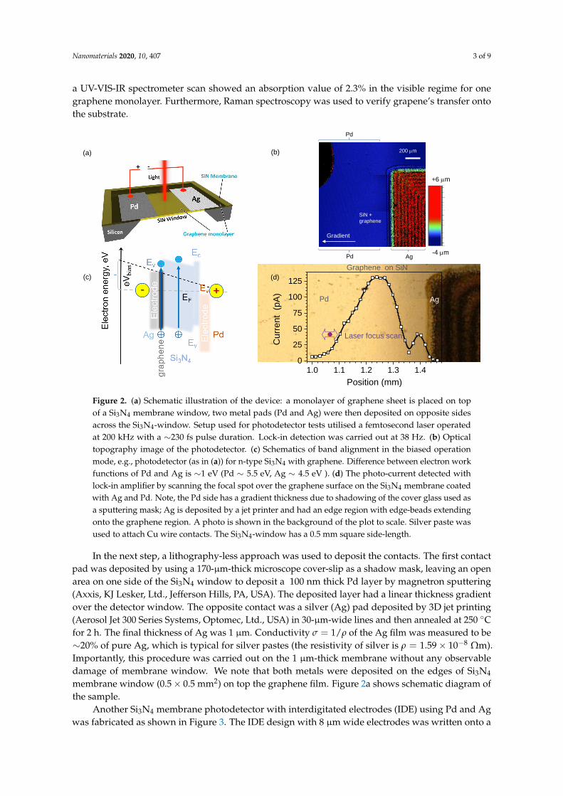
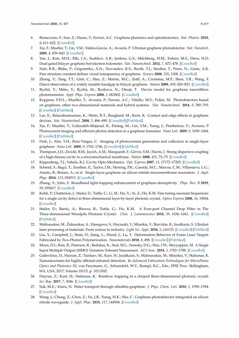
In this work, the initial sample consists of a 7.5× 7.5 mm2 Si substrate with a 1 µm thick Si3N4
film suspended over a 500× 500 µm2 etched square in Si (Norcada, Ltd., Edmonton, AB, Canada)as shown in Figure 2a. A graphene sheet (ACS Material, Ltd., USA), estimated thickness 3.4 Å [27])was transferred onto the substrate, centered over the Si3N4 window. Resistance of the graphene sheet(1 kΩ/sq) was measured by 4-point probe (Jandel Engineering Ltd., Leighton Buzzard, UK) and
Nanomaterials 2020, 10, 407 3 of 9
a UV-VIS-IR spectrometer scan showed an absorption value of 2.3% in the visible regime for onegraphene monolayer. Furthermore, Raman spectroscopy was used to verify grapene’s transfer ontothe substrate.
1.0 1.1 1.2 1.3 1.40
25
50
75
100
125C
urr
en
t (
pA
)
Position (mm)
(a)
Pd Ag
Laser focus scan
Graphene on SiN
(d)
heig
ht
mem
bra
ne
SiN +
graphene
Ag
Pd
+6 mm
200 mm
-4 mmPd
(b)
Gradient
(c)
Figure 2. (a) Schematic illustration of the device: a monolayer of graphene sheet is placed on topof a Si3N4 membrane window, two metal pads (Pd and Ag) were then deposited on opposite sidesacross the Si3N4-window. Setup used for photodetector tests utilised a femtosecond laser operatedat 200 kHz with a ∼230 fs pulse duration. Lock-in detection was carried out at 38 Hz. (b) Opticaltopography image of the photodetector. (c) Schematics of band alignment in the biased operationmode, e.g., photodetector (as in (a)) for n-type Si3N4 with graphene. Difference between electron workfunctions of Pd and Ag is ∼1 eV (Pd ∼ 5.5 eV, Ag ∼ 4.5 eV ). (d) The photo-current detected withlock-in amplifier by scanning the focal spot over the graphene surface on the Si3N4 membrane coatedwith Ag and Pd. Note, the Pd side has a gradient thickness due to shadowing of the cover glass used asa sputtering mask; Ag is deposited by a jet printer and had an edge region with edge-beads extendingonto the graphene region. A photo is shown in the background of the plot to scale. Silver paste wasused to attach Cu wire contacts. The Si3N4-window has a 0.5 mm square side-length.
In the next step, a lithography-less approach was used to deposit the contacts. The first contactpad was deposited by using a 170-µm-thick microscope cover-slip as a shadow mask, leaving an openarea on one side of the Si3N4 window to deposit a 100 nm thick Pd layer by magnetron sputtering(Axxis, KJ Lesker, Ltd., Jefferson Hills, PA, USA). The deposited layer had a linear thickness gradientover the detector window. The opposite contact was a silver (Ag) pad deposited by 3D jet printing(Aerosol Jet 300 Series Systems, Optomec, Ltd., USA) in 30-µm-wide lines and then annealed at 250 Cfor 2 h. The final thickness of Ag was 1 µm. Conductivity σ = 1/ρ of the Ag film was measured to be∼20% of pure Ag, which is typical for silver pastes (the resistivity of silver is ρ = 1.59× 10⁻⁸ Ωm).Importantly, this procedure was carried out on the 1 µm-thick membrane without any observabledamage of membrane window. We note that both metals were deposited on the edges of Si3N4
membrane window (0.5× 0.5 mm2) on top the graphene film. Figure 2a shows schematic diagram ofthe sample.
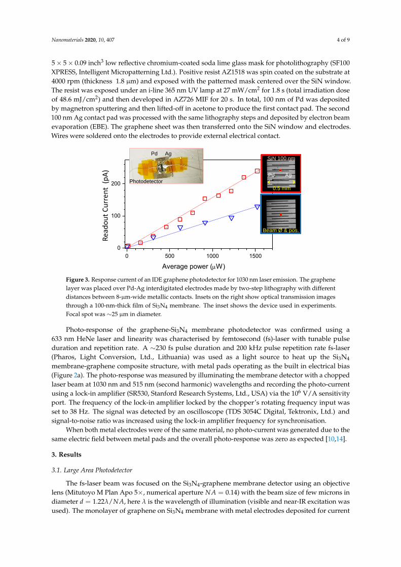
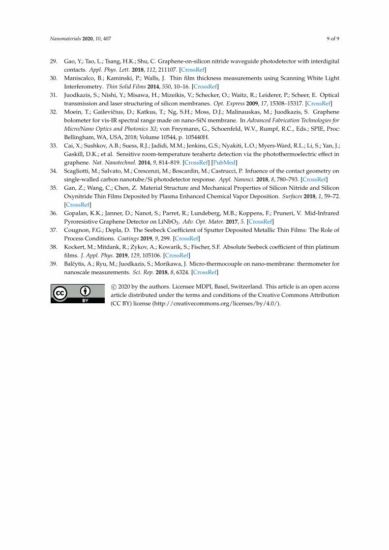
Another Si3N4 membrane photodetector with interdigitated electrodes (IDE) using Pd and Agwas fabricated as shown in Figure 3. The IDE design with 8 µm wide electrodes was written onto a
Nanomaterials 2020, 10, 407 4 of 9
5× 5× 0.09 inch3 low reflective chromium-coated soda lime glass mask for photolithography (SF100XPRESS, Intelligent Micropatterning Ltd.). Positive resist AZ1518 was spin coated on the substrate at4000 rpm (thickness 1.8 µm) and exposed with the patterned mask centered over the SiN window.The resist was exposed under an i-line 365 nm UV lamp at 27 mW/cm2 for 1.8 s (total irradiation doseof 48.6 mJ/cm2) and then developed in AZ726 MIF for 20 s. In total, 100 nm of Pd was depositedby magnetron sputtering and then lifted-off in acetone to produce the first contact pad. The second100 nm Ag contact pad was processed with the same lithography steps and deposited by electron beamevaporation (EBE). The graphene sheet was then transferred onto the SiN window and electrodes.Wires were soldered onto the electrodes to provide external electrical contact.
0 500 1000 1500
0
100
200
Redout voltage (V
)
Average power (W)
0.5 mm
Photodetector
Pd Ag
Pd AgSiN 100 nm
Beam Ø & pos.
Rea
do
ut
Cu
rren
t(p
A)
Figure 3. Response current of an IDE graphene photodetector for 1030 nm laser emission. The graphenelayer was placed over Pd-Ag interdigitated electrodes made by two-step lithography with differentdistances between 8-µm-wide metallic contacts. Insets on the right show optical transmission imagesthrough a 100-nm-thick film of Si3N4 membrane. The inset shows the device used in experiments.Focal spot was ∼25 µm in diameter.
Photo-response of the graphene-Si3N4 membrane photodetector was confirmed using a633 nm HeNe laser and linearity was characterised by femtosecond (fs)-laser with tunable pulseduration and repetition rate. A ∼230 fs pulse duration and 200 kHz pulse repetition rate fs-laser(Pharos, Light Conversion, Ltd., Lithuania) was used as a light source to heat up the Si3N4
membrane-graphene composite structure, with metal pads operating as the built in electrical bias(Figure 2a). The photo-response was measured by illuminating the membrane detector with a choppedlaser beam at 1030 nm and 515 nm (second harmonic) wavelengths and recording the photo-currentusing a lock-in amplifier (SR530, Stanford Research Systems, Ltd., USA) via the 106 V/A sensitivityport. The frequency of the lock-in amplifier locked by the chopper’s rotating frequency input wasset to 38 Hz. The signal was detected by an oscilloscope (TDS 3054C Digital, Tektronix, Ltd.) andsignal-to-noise ratio was increased using the lock-in amplifier frequency for synchronisation.
When both metal electrodes were of the same material, no photo-current was generated due to thesame electric field between metal pads and the overall photo-response was zero as expected [10,14].
3. Results
3.1. Large Area Photodetector
The fs-laser beam was focused on the Si3N4-graphene membrane detector using an objectivelens (Mitutoyo M Plan Apo 5×, numerical aperture NA = 0.14) with the beam size of few microns indiameter d = 1.22λ/NA, here λ is the wavelength of illumination (visible and near-IR excitation wasused). The monolayer of graphene on Si3N4 membrane with metal electrodes deposited for current
Nanomaterials 2020, 10, 407 5 of 9
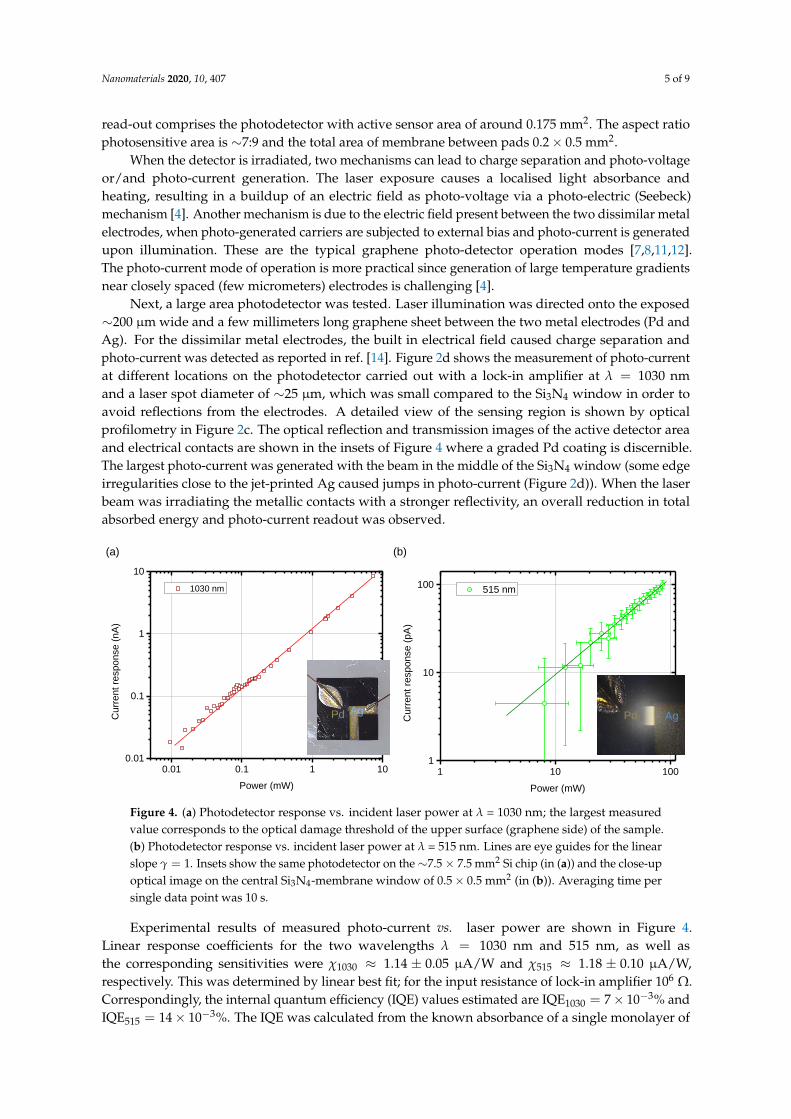
read-out comprises the photodetector with active sensor area of around 0.175 mm2. The aspect ratiophotosensitive area is ∼7:9 and the total area of membrane between pads 0.2× 0.5 mm2.
When the detector is irradiated, two mechanisms can lead to charge separation and photo-voltageor/and photo-current generation. The laser exposure causes a localised light absorbance andheating, resulting in a buildup of an electric field as photo-voltage via a photo-electric (Seebeck)mechanism [4]. Another mechanism is due to the electric field present between the two dissimilar metalelectrodes, when photo-generated carriers are subjected to external bias and photo-current is generatedupon illumination. These are the typical graphene photo-detector operation modes [7,8,11,12].The photo-current mode of operation is more practical since generation of large temperature gradientsnear closely spaced (few micrometers) electrodes is challenging [4].
Next, a large area photodetector was tested. Laser illumination was directed onto the exposed∼200 µm wide and a few millimeters long graphene sheet between the two metal electrodes (Pd andAg). For the dissimilar metal electrodes, the built in electrical field caused charge separation andphoto-current was detected as reported in ref. [14]. Figure 2d shows the measurement of photo-currentat different locations on the photodetector carried out with a lock-in amplifier at λ = 1030 nmand a laser spot diameter of ∼25 µm, which was small compared to the Si3N4 window in order toavoid reflections from the electrodes. A detailed view of the sensing region is shown by opticalprofilometry in Figure 2c. The optical reflection and transmission images of the active detector areaand electrical contacts are shown in the insets of Figure 4 where a graded Pd coating is discernible.The largest photo-current was generated with the beam in the middle of the Si3N4 window (some edgeirregularities close to the jet-printed Ag caused jumps in photo-current (Figure 2d)). When the laserbeam was irradiating the metallic contacts with a stronger reflectivity, an overall reduction in totalabsorbed energy and photo-current readout was observed.
(a) (b)
0.01 0.1 1 100.01
0.1
1
10
1030 nm
Cu
rre
nt
respo
nse
(n
A)
Power (mW)
Pd Ag
1 10 1001
10
100
515 nm
Curr
ent re
sponse (
pA
)
Power (mW)
AgPd
Figure 4. (a) Photodetector response vs. incident laser power at λ = 1030 nm; the largest measuredvalue corresponds to the optical damage threshold of the upper surface (graphene side) of the sample.(b) Photodetector response vs. incident laser power at λ = 515 nm. Lines are eye guides for the linearslope γ = 1. Insets show the same photodetector on the∼7.5× 7.5 mm2 Si chip (in (a)) and the close-upoptical image on the central Si3N4-membrane window of 0.5× 0.5 mm2 (in (b)). Averaging time persingle data point was 10 s.
Experimental results of measured photo-current vs. laser power are shown in Figure 4.Linear response coefficients for the two wavelengths λ = 1030 nm and 515 nm, as well asthe corresponding sensitivities were χ1030 ≈ 1.14 ± 0.05 µA/W and χ515 ≈ 1.18 ± 0.10 µA/W,respectively. This was determined by linear best fit; for the input resistance of lock-in amplifier 106 Ω.Correspondingly, the internal quantum efficiency (IQE) values estimated are IQE1030 = 7× 10⁻³% andIQE515 = 14× 10−3%. The IQE was calculated from the known absorbance of a single monolayer of
Nanomaterials 2020, 10, 407 6 of 9
graphene and photon flux (photons per second), i.e., incident photon conversion to electrons generatedwhich are collected (the internal EQ). IQE = 100% corresponds to every photon-generated chargecarrier pair being collected at the electrodes.
The experimentally measured sensitivity values might appear lower than those of the mostefficient photodetectors [7]. However, the responsivity values compare favorably with other types ofgraphene-on-Si3N4 photodetectors. The responsivity of the wave-guide enhanced configuration wasreported to be ∼0.1 [28] and ∼0.32 mA/W [29] for the zero-biased operation. In addition, the designof the reported detector might allow it to detect light inside a 3D photonic crystal without perturbingtransmission/reflection spectra due to its small form-factor.
Illumination of photodetector at the fourth harmonic at 257 nm wavelength was also tested.However, it was not possible to detect a change in current using irradiation doses less than the damagethreshold for the Si3N4 membrane surface caused by strong absorption (NA = 0.4 Mitutoyo near-UVobjective lens optimised for high transmission at 257 nm). The transmission spectra of Si3N4 membraneconfirmed a strong absorption at in the UV spectral range (not shown here). For around λ = 1 µm(the thickness of the Si3N4 membrane d = 2 µm), the expected value of the absorbtion coefficientis around α ∼ 1.0 [cm−1] [30]. Depending on the thickness, the Fabry–Perot interference in the SiNmembrane significantly modulates transmission, which can be used to increase detection selectivity atspecific wavelengths or to render the membrane transparent even at a high irradiance [31].
3.2. Photodetector for a Small Detection Area
The miniaturisation of the initial photodetector on a micro-Si3N4 membrane was tested earlierwith a 4.5 µm gap width and dissimilar metal (Cr, Ag) electrodes [32] and was demonstrated on a bulksubstrate [33].
Here, a more practical approach was taken, as opposed to high-resolution electron beamlithography [32]. The photodetector was defined by simple contact photolithography on a 100-nm-thickSi3N4-membrane and fabricated using magnetron sputtering of Pd and electron beam evaporationof Ag. The deposited layers were 35 nm thick. By alignment of the second pattern, the gap betweenthe dissimilar metal electrodes could be made as required during the contact step (insets in Figure 3).Differently from the earlier described photodetector, the membrane was 10 times thinner and thegraphene was transferred in the last step over the fabricated contacts. This further simplifies thefabrication of the thin photodetector. Slightly lower photo-sensitivity was observed (Figure 3) ascompared with the device, where contacts were made over the graphene (Figure 4). A conformalgraphene coating over the contacts and Si3N4-membrane was expected.
The partial transparency of the thin layer of Si3N4 in the visible and near-IR spectral ranges [30]is beneficial for transmission based optical devices. Specifically, 3D direct-laser-write fabricationprocesses [22] can be used for creating 3D structures on both sides of the photodetector. The benefitof such a photodetector could open up various multi-layer spatially integrable structures to be usedin combination with thin-film photodetectors, which can operate in the biased as well as unbiasedmodes [34]; see the schematics in Figure 1a.
It is significant that a 100 nm thick Si3N4 membrane is resilient enough for multiple manualsubmersions in three different solvents over several fabrication steps. Therefore it is possible to usein complicated multi-step additive fabrication processes and benefit from mechanical properties ofoptically thin Si3N4 [35].
Future improvements are expected when a pyroelectric sub-micrometer-thin film of lithiumniobate (or PZT) is placed below the graphene instead of the Si3N4 membrane. The pyroelectriclayer generates bound charges under heating, which causes bandgap opening in graphene. It makesgraphene function as a doped semiconductor. This feature can be utilised to allow detection byphoto-voltage or photo-current [12]. The electron density induced in graphene is n = γ(T)T/e,where γ(T) is the temperature dependent pyroelectric coefficient, e is the electron charge, and T isthe temperature increase [36]. Hence, optical absorption affects conductivity, which is a considerably
Nanomaterials 2020, 10, 407 7 of 9
stronger effect than the Seebeck mechanism, which generates low photo-voltage ∆V = S∇T even forthe large Seebeck constant S of graphene [36]. The gradient thickness of metal contact used in thisstudy can be also useful for measurement of the Seebeck constant of metal nanofilms, where it dependson the mean free path of electrons and phonon drag [37,38], and has to be experimentally determinedfor precise temperature measurements at the nanoscale [39].
4. Conclusions and Outlook
We demonstrate a photodetector made by lithography-free methods combining a simplegraphene-to-Si3N4 membrane transfer method with jet-printing and magnetron sputtering for contactdeposition. Sensitivity of the photodetector was ∼1.1 µA/W at both 1030 and 515 nm wavelengthswhen the Si3N4 membrane was 1 µm-thick. In addition, standard photolithography was used to definephotodetector contacts on a 100-nm-thick Si3N4 membrane showing further miniaturization feasibilityfor visible and near-IR radiation detection at the nanoscale.
The two demonstrated modalities of photodetector fabrication via (1) lithography-free anddirect-write of metal electrodes and (2) two-step photolithography on sub-micrometer-thickmembranes opens new possibilities for the miniaturisation and integration of photodetectors. The newcapability to embed such spectrally broad photodetectors into integrated systems, including thosethat can be 3D laser printed, is a promising direction (Figure 1). The sensitivity of such low-mass andtransparent detectors need to be low so it is barely “visible” for the slow light (multiple reflections andinterference) inside 3D photonic crystals.
The proposed photodetector was inferior to the current mature silicon photodetector technologyin terms of sensitivity as it was not designed for maximum absorbance. However, for the particularfunction of detecting light inside 3D photonic structures without perturbation, the low sensitivity(invisibility) is the required property.
The proposed simple fabrication of photodetectors with sub-wavelength thickness can findapplications in wearable opto-electronics and monitoring sensor applications.
Author Contributions: Conceptualization of thin photodetector T.M., D.G., S.J.; conceptualization of detectionof stopped light and modeling K.S., H.K., V.M.; fabrication of demonstrative photonic crystals V.M., D.G., T.K.,M.M.; fabrication of photodetectors T.M., D.G., T.K., S.H.N., S.L.; measurements of light detection D.G., T.M., T.K.;writing–original draft S.J., T.M., D.G.; D.J.M. provided critical insights, discussion of results and editing—all theauthors. All authors have read and agreed to the published version of the manuscript.
Funding: NATO grant No. SPS-985048 is acknowledged for funding. V.M. acknowledges support by JST CRESTGrant Number PMJCR19I3, Japan.
Acknowledgments: We are grateful to P. R. Stoddart, S. Beguin, V. Dislakis for help with Ag inkjet printing andto T. Malinauskas (Vilnius University) for his helpful insight on the characterization procedure. D.G. is grateful toFemtika LTD for additional support. We acknowledge technology transfer project with WOP—Altechna Ltd. forfs-fabrication station installed in Swinburne.
Conflicts of Interest: The authors declare no conflict of interest.
References
1. Mak, K.F.; Sfeir, M.Y.; Wu, Y.; Lui, C.H.; Misewich, J.A.; Heinz, T.F. Measurement of the optical conductivityof graphene. Phys. Rev. Lett. 2008, 101, 196405. [CrossRef] [PubMed]
2. Li, Z.Q.; Henriksen, E.A.; Jiang, Z.; Hao, Z.; Martin, M.C.; Kim, P.; Stormer, H.L.; Basov, D.N. Dirac chargedynamics in graphene by infrared spectroscopy. Nat. Phys. 2008, 4, 532–535. [CrossRef]
3. Wang, F.; Zhang, Y.; Tian, C.; Girit, C.; Zettl, A.; Crommie, M.; Shen, Y.R. Gate-variable optical transitions ingraphene. Science 2008, 320, 206–209. [CrossRef] [PubMed]
4. Mueller, T.; Xia, F.; Avouris, P. Graphene photodetectors for high-speed optical communications. Nat. Photon.2010, 4, 297–301. [CrossRef]
5. Castro Neto, H.; Guinea, F.; Peres, N.; Novoselov, K.S.; Geim, A.K. The electronic properties of graphene.Rev. Mod. Phys. 2009, 81, 109–162. [CrossRef]
Nanomaterials 2020, 10, 407 8 of 9
6. Bonaccorso, F.; Sun, Z.; Hasan, T.; Ferrari, A.C. Graphene photonics and optoelectronics. Nat. Photon. 2010,4, 611–622. [CrossRef]
7. Xia, F.; Mueller, T.; Lin, Y.M.; Valdes-Garcia, A.; Avouris, P. Ultrafast graphene photodetector. Nat. Nanotech.2009, 4, 839–843. [CrossRef]
8. Yan, J.; Kim, M.H.; Elle, J.A.; Sushkov, A.B.; Jenkins, G.S.; Milchberg, H.M.; Fuhrer, M.S.; Drew, H.D.Dual-gated bilayer graphene hot-electron bolometer. Nat. Nanotechnol. 2012, 7, 472–478. [CrossRef]
9. Nair, R.R.; Blake, P.; Grigorenko, A.N.; Novoselov, K.S.; Booth, T.J.; Stauber, T.; Peres, N.; Geim, A.K.Fine structure constant defines visual transparency of graphene. Science 2008, 320, 1308. [CrossRef]
10. Zhang, Y.; Tang, T.T.; Girit, C.; Hao, Z.; Martin, M.C.; Zettl, A.; Crommie, M.F.; Shen, Y.R.; Wang, F.Direct observation of a widely tunable bandgap in bilayer graphene. Nature 2009, 459, 820–823. [CrossRef]
11. Ryzhii, V.; Mitin, V.; Ryzhii, M.; Ryabova, N.; Otsuji, T. Device model for graphene nanoribbonphototransistor. Appl. Phys. Express 2008, 1, 063002. [CrossRef]
12. Koppens, F.H.L.; Mueller, T.; Avouris, P.; Ferrari, A.C.; Vitiello, M.S.; Polini, M. Photodetectors basedon graphene, other two-dimensional materials and hybrid systems. Nat. Nanotechnol. 2014, 9, 780–793.[CrossRef] [PubMed]
13. Lee, E.; Balasubramanian, K.; Weitz, R.T.; Burghard, M.; Kern, K. Contact and edge effects in graphenedevices. Nat. Nanotechnol. 2008, 3, 486–490. [CrossRef] [PubMed]
14. Xia, F.; Mueller, T.; Golizadeh-Mojarad, R.; Freitag, M.; Lin, Y.M.; Tsang, J.; Perebeinos, V.; Avouris, P.Photocurrent imaging and efficient photon detection in a graphene transistor. Nano Lett. 2009, 9, 1039–1044.[CrossRef] [PubMed]
15. Park, J.; Ahn, Y.H.; Ruiz-Vargas, C. Imaging of photocurrent generation and collection in single-layergraphene. Nano Lett. 2009, 9, 1742–1746. [CrossRef] [PubMed]
16. Thompson, J.D.; Zwickl, B.M.; Jayich, A.M.; Marquardt, F.; Girvin, S.M.; Harris, J. Strong dispersive couplingof a high-finesse cavity to a micromechanical membrane. Nature 2008, 452, 72–75. [CrossRef]
17. Kippenberg, T.J.; Vahala, K.J. Cavity Opto-Mechanics. Opt. Express 2007, 15, 17172–17205. [CrossRef]18. Schmid, S.; Bagci, T.; Zeuthen, E.; Taylor, J.M.; Herring, P.K.; Cassidy, M.C.; Marcus, C.M.; Villanueva, L.G.;
Amato, B.; Boisen, A.; et al. Single-layer graphene on silicon nitride micromembrane resonators. J. Appl.Phys. 2014, 115, 054513. [CrossRef]
19. Zhang, X.; John, S. Broadband light-trapping enhancement of graphene absorptivity. Phys. Rev. B 2019,99, 035417. [CrossRef]
20. Kohli, P.; Chatterton, J.; Stieler, D.; Tuttle, G.; Li, M.; Hu, X.; Ye, Z.; Ho, K.M. Fine tuning resonant frequenciesfor a single cavity defect in three-dimensional layer-by-layer photonic crystal. Optics Express 2008, 16, 19844.[CrossRef]
21. Stieler, D.; Barsic, A.; Biswas, R.; Tuttle, G.; Ho, K.M. A Four-port Channel Drop Filter in TheThree-dimensional Woodpile Photonic Crystal. Chin. J. Luminescence 2018, 39, 1036–1041. [CrossRef][PubMed]
22. Malinauskas, M.; Žukauskas, A.; Hasegawa, S.; Hayasaki, Y.; Mizeikis, V.; Buividas, R.; Juodkazis, S. Ultrafastlaser processing of materials: From science to industry. Light Sci. Appl. 2016, 5, e16133. [CrossRef] [PubMed]
23. Liu, Y.; Campbell, J.; Stein, O.; Jiang, L.; Hund, J.; Lu, Y. Deformation Behavior of Foam Laser TargetsFabricated by Two-Photon Polymerization. Nanomaterials 2018, 8, 498. [CrossRef] [PubMed]
24. Moon, D.I.; Kim, B.; Peterson, R.; Badokas, K.; Seol, M.L.; Senesky, D.G.; Han, J.W.; Meyyappan, M. A SingleInput Multiple Output (SIMO) Variation-Tolerant Nanosensor. ACS Sens. 2018, 3, 1782–1788. [CrossRef]
25. Gailevicius, D.; Hayran, Z.; Turduev, M.; Kurt, H.; Juodkazis, S.; Malinauskas, M.; Mizeikis, V.; Staliunas, K.Nanostructures for highly efficient infrared detection. In Advanced Fabrication Technologies for Micro/NanoOptics and Photonics XI; von Freymann, G., Schoenfeld, W.V., Rumpf, R.C., Eds.; SPIE Proc: Bellingham,WA, USA, 2017; Volume 10115, p. 101150Z.
26. Hayran, Z.; Kurt, H.; Staliunas, K. Rainbow trapping in a chirped three-dimensional photonic crystal.Sci. Rep. 2017, 7, 3046. [CrossRef]
27. Suk, M.E.; Aluru, N. Water transport through ultrathin graphene. J. Phys. Chem. Lett. 2010, 1, 1590–1594.[CrossRef]
28. Wang, J.; Cheng, Z.; Chen, Z.; Xu, J.B.; Tsang, H.K.; Shu, C. Graphene photodetector integrated on siliconnitride waveguide. J. Appl. Phys. 2015, 117, 144504. [CrossRef]
Nanomaterials 2020, 10, 407 9 of 9
29. Gao, Y.; Tao, L.; Tsang, H.K.; Shu, C. Graphene-on-silicon nitride waveguide photodetector with interdigitalcontacts. Appl. Phys. Lett. 2018, 112, 211107. [CrossRef]
30. Maniscalco, B.; Kaminski, P.; Walls, J. Thin film thickness measurements using Scanning White LightInterferometry. Thin Solid Films 2014, 550, 10–16. [CrossRef]
31. Juodkazis, S.; Nishi, Y.; Misawa, H.; Mizeikis, V.; Schecker, O.; Waitz, R.; Leiderer, P.; Scheer, E. Opticaltransmission and laser structuring of silicon membranes. Opt. Express 2009, 17, 15308–15317. [CrossRef]
32. Moein, T.; Gailevicius, D.; Katkus, T.; Ng, S.H.; Moss, D.J.; Malinauskas, M.; Juodkazis, S. Graphenebolometer for vis-IR spectral range made on nano-SiN membrane. In Advanced Fabrication Technologies forMicro/Nano Optics and Photonics XI; von Freymann, G., Schoenfeld, W.V., Rumpf, R.C., Eds.; SPIE, Proc:Bellingham, WA, USA, 2018; Volume 10544, p. 105440H.
33. Cai, X.; Sushkov, A.B.; Suess, R.J.; Jadidi, M.M.; Jenkins, G.S.; Nyakiti, L.O.; Myers-Ward, R.L.; Li, S.; Yan, J.;Gaskill, D.K.; et al. Sensitive room-temperature terahertz detection via the photothermoelectric effect ingraphene. Nat. Nanotechnol. 2014, 9, 814–819. [CrossRef] [PubMed]
34. Scagliotti, M.; Salvato, M.; Crescenzi, M.; Boscardin, M.; Castrucci, P. Infuence of the contact geometry onsingle-walled carbon nanotube/Si photodetector response. Appl. Nanosci. 2018, 8, 780–793. [CrossRef]
35. Gan, Z.; Wang, C.; Chen, Z. Material Structure and Mechanical Properties of Silicon Nitride and SiliconOxynitride Thin Films Deposited by Plasma Enhanced Chemical Vapor Deposition. Surfaces 2018, 1, 59–72.[CrossRef]
36. Gopalan, K.K.; Janner, D.; Nanot, S.; Parret, R.; Lundeberg, M.B.; Koppens, F.; Pruneri, V. Mid-InfraredPyroresistive Graphene Detector on LiNbO3. Adv. Opt. Mater. 2017, 5. [CrossRef]
37. Cougnon, F.G.; Depla, D. The Seebeck Coefficient of Sputter Deposited Metallic Thin Films: The Role ofProcess Conditions. Coatings 2019, 9, 299. [CrossRef]
38. Kockert, M.; Mitdank, R.; Zykov, A.; Kowarik, S.; Fischer, S.F. Absolute Seebeck coefficient of thin platinumfilms. J. Appl. Phys. 2019, 129, 105106. [CrossRef]
39. Balcytis, A.; Ryu, M.; Juodkazis, S.; Morikawa, J. Micro-thermocouple on nano-membrane: thermometer fornanoscale measurements. Sci. Rep. 2018, 8, 6324. [CrossRef]
c© 2020 by the authors. Licensee MDPI, Basel, Switzerland. This article is an open accessarticle distributed under the terms and conditions of the Creative Commons Attribution(CC BY) license (http://creativecommons.org/licenses/by/4.0/).


![Graphene modelocked VECSELs · Ultrafast vertical-external-cavity surface -emitting lasers (VECSELs )[4], also known as semiconductor disk lasers (SDLs) [5] or optically pumped semiconductor](https://img.pdfslide.net/doc/110x75/5f09805b7e708231d4272096/graphene-modelocked-vecsels-ultrafast-vertical-external-cavity-surface-emitting.jpg)


![SPG MITTEILUNGEN COMMUNICATIONS DE LA SSP AUSZUG - … · 40 GHz [9]. A metal-graphene-metal photodetector, consist-ing of a large number of inter-digitated finger electrodes, was](https://img.pdfslide.net/doc/110x75/5eac39525a15332384155c26/spg-mitteilungen-communications-de-la-ssp-auszug-40-ghz-9-a-metal-graphene-metal.jpg)