Embed Size (px)
Citation preview
P-11: Electrical Properties and Stability of Dual-Gate Coplanar Homojunction Amorphous Indium-Gallium-Zinc-Oxide Thin-Film Transistor
Gwanghyeon Baek, Alex Kuo, Jerzy Kanicki Dept. of Electrical Engineering and Computer Science, University of Michigan, Ann Arbor, MI, USA
Katsumi Abe and Hideya Kumomi Cannon Research Center, Cannon Inc., Ohta-Ku, Tokyo, Japan
Abstract The electrical characteristics and stabilities of dual-gate (DG) coplanar homojunction amorphous indium-gallium-zinc-oxide thin-film transistors (a-IGZO TFTs) are described. When the gate voltage is applied on top and bottom electrodes, the DG a-IGZO TFT showed an excellent electrical performance with the sub-threshold swing of 99 mV/dec, the mobility of 15.1 cm2/V·s and the on-off ratio of 109. Under positive bias temperature stress, the device threshold voltage shifts about +4.5V after 10,000 seconds, while its shifts under negative bias temperature stress are very small. The effect of TFT illumination is also discussed.
1. Introduction It is well known that the metal-oxide-semiconductor field effect transistors can have a better electrical performance when a larger portion of channel area is controlled by an additional gate electrode. [1] The dual-gate or double-gate (DG) structure has already been proposed for a sub-micron silicon complimentary metal-oxide-semiconductor (CMOS). The DG amorphous silicon (a-Si:H) TFTs have also been investigated to provide an effective light shielding that guarantee the TFT’s electrical reliability under illumination. [2, 3] However, the presence of bias on the additional gate electrode introduces unwanted shifts in a-Si:H TFT sub-threshold swing (SS) and threshold voltage. To address this problem, the additional gate electrode has been grounded to provide reliable circuit operation in a pixel array. [3, 4]We believe that the dual-gate a-IGZO TFT structure has the advantage of producing an enhanced device performance and stability under light illumination.
It was previously reported that the coplanar homojunction a-IGZO TFT has a good ohmic source/drain (S/D) junction and is capable of achieving small channel lengths. [5, 6] In this paper, we describe the DG coplanar homojunction a-IGZO TFT electrical characteristics, and stability under bias temperature stress (BTS) and under illumination.
2. Experimental
2.1. a-IGZO TFT structure Figure 1 shows processing step during the DG TFT fabrication. [5] To form a bottom gate electrode, a 100 nm-thick Mo film was deposited by a direct-current sputtering on glass substrate (Corning 1737) and patterned to form the bottom gate electrode (a). A 200 nm-thick SiOx layer was deposited by plasma enhanced chemical vapor deposition (PECVD) at 340 °C which will be used as a bottom gate insulator (b). The a-IGZO film (30 nm) was D.C. sputtered at room temperature and defined using a diluted hydrochloric acid (c). A 150 nm a-SiOX channel protection layer (CPL) was sputtered and patterned by dry etching (d). The CPL defines the TFT width (W) and length (L). The CPL
Figure 1 A schematic representation of the processing steps used during the DG TFT fabrication.
patterning was followed by a PECVD at 250 °C of bi-layer passivation of 300 nm-thick amorphous silicon nitride (a-SiNX:H) and 50 nm-thick a-SiOX. During the a-SiNX:H PECVD process, hydrogen in the reactive PECVD chamber and/or in the a-SiNX:H layer dopes the exposed a-IGZO region and increases its electrical conductivity (e). Next the contact vias were formed in top passivation bi-layer by dry etching (f), followed by the sputtering and patterning of 100 nm-thick Mo source/drain electrodes. At the same time the Mo top gate is formed (g). It should be noticed that in such device structure Mo metal gate and source/drain contacts do not overlap; although there is some overlap between Mo metal gate and the hydrogen doped S/D contact regions. There is sepera-
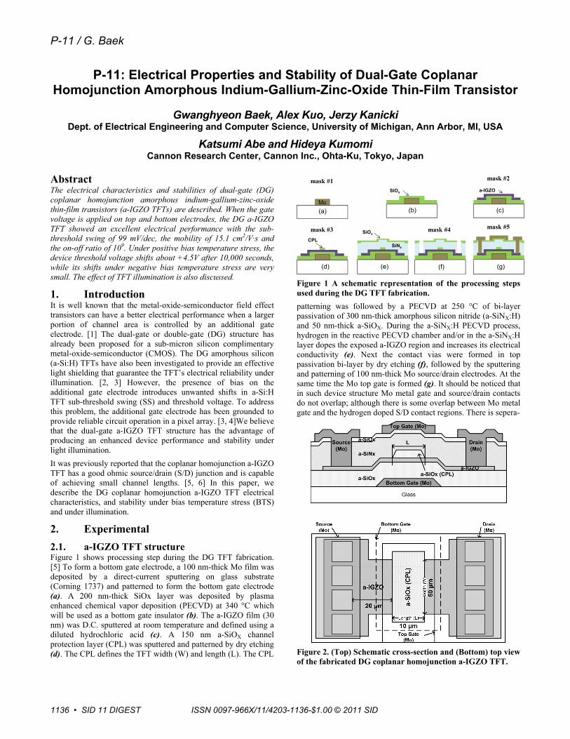
Figure 2. (Top) Schematic cross-section and (Bottom) top view of the fabricated DG coplanar homojunction a-IGZO TFT.
Mo
SiOx a-IGZO
CPLSiNx
(a) (b) (c)
(d) (e) (g)(f)
mask #1 mask #2
mask #3 mask #4 mask #5SiOx
P-11 / G. Baek
1136 • SID 11 DIGEST ISSN 0097-966X/11/4203-1136-$1.00 © 2011 SID
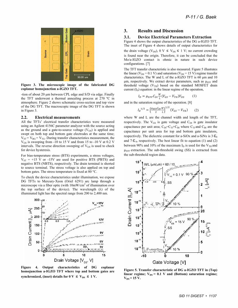
Figure 3. The microscopic image of the fabricated DG coplanar homojunction a-IGZO TFT.
-tion of about 20 μm between CPL edge and S/D via edge. Finally the TFT underwent a thermal annealing process at 270 ºC in atmosphere. Figure 2 shows schematic cross-section and top view of the DG TFT. The macroscopic image of the DG TFT is shown in Figure 3.
2.2. Electrical measurements All the TFTs’ electrical transfer characteristics were measured using an Agilent 4156C parameter analyzer with the source acting as the ground and a gate-to-source voltage (VGS) is applied and swept on both top and bottom gate electrodes at the same time; VST = VBG = VTG. During transfer characteristics measurement, the VGS is sweeping from -10 to 15 V and from 15 to -10 V at 0.2 V intervals. The reverse direction sweeping of VGS is used to check for device hysteresis.
For bias-temperature stress (BTS) experiments, a stress voltages, VST = +15 V or -15V are used for positive BTS (PBTS) and negative BTS (NBTS), respectively. The drain terminal is shorted to source terminal. The stress voltage is also applied on top and bottom gates. The stress temperature is fixed at 80 °C.
To check the device characteristics under illumination, we expose DG TFTs to Mercury-Xeon (Oriel 6291) arc lamp through a microscope via a fiber optic (with 10mW/cm2 of illumination over the top surface of the device). The wavelength (λ) of the illuminated light has the spectral range from 200 to 2,400 nm.
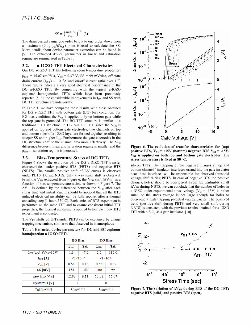
Figure 4. Output characteristics of DG coplanar homojunction a-IGZO TFT where top and bottom gates are
synchronized, (inset) details for 0 V ≤ VDS ≤ 1 V.
3. Results and Discussion 3.1. Device Electrical Parameters Extraction Figure 4 shows the output characteristics of the DG a-IGZO TFT. The inset of Figure 4 shows details of output characteristics for
the drain voltage (VDS), 0 V ≤ VDS ≤ 1 V; no current crowding is found near the origin. Therefore, it can be concluded that the Mo/a-IGZO contact is ohmic in nature in such device configurations. [7]
The TFT transfer characteristic is also measured. Figure 5 illustrates the linear (VDS = 0.1 V) and saturation (VDS = 15 V) regime transfer characteristics. The W and L of the a-IGZO TFT is 60 μm and 10 μm, respectively. We extract device parameters, such as µEFF and threshold voltage (VTH) based on the standard MOSFET drain current (ID) equation: in the linear regime of the operation,
(1)
and in the saturation regime of the operation. [8]
(2)
where W and L are the channel width and length of the TFT, respectively. The VGS is gate voltage and CDI is gate insulator capacitance per unit area; CDI=CTI+CBI where CTI and CBI are the capacitance per unit area for top and bottom gate insulators, respectively. The dielectric constant for a-SiOx and a-SiNx is 3·ε0 and 7·ε 0, respectively. The best linear fit to equation (1) and (2) between 90% and 10% of the maximum ID is used for the VTH and µEFF extraction. The sub-threshold swing (SS) is extracted from the sub-threshold region data.
Figure 5. Transfer characteristic of DG a-IGZO TFT in (Top) linear regime; VDS = 0.1 V and (Bottom) saturation regime; VDS = 15 V.
( )
{
} ( )
P-11 / G. Baek
SID 11 DIGEST • 1137
(3)
The drain current range one order below to one order above from a maximum (∂logI ∂V⁄ ) point is used to calculate the SS. More details about device parameter extraction can be found in [9]. The extracted device parameters in linear and saturation regime are summarized in Table 1.
3.2. a-IGZO TFT Electrical Characteristics Our DG a-IGZO TFT has following room temperature properties:
μEFF = 15.07 cm2/V·s, VTH = 0.37 V, SS = 99 mV/dec, off-state drain current (IOFF) ~ 10-13A and on-off current ratio over 109. These results indicate a very good electrical performance of the DG a-IGZO TFT. By comparing with the typical a-IGZO coplanar homojunction TFTs which have been previously reported [5, 6], the considerable improvements in ION and SS with DG TFT structure are noteworthy.
In Table 1, we have compared these results with those obtained for DG a-IGZO TFT with bottom gate (BG) bias condition. For BG bias condition, the VGS is applied only on bottom gate while the top gate is grounded. The BG TFT structure is similar to a traditional TFT structure. In DG a-IGZO TFT, since the VGS is applied on top and bottom gate electrodes, two channels on top and bottom sides of a-IGZO layer are formed together resulting in steeper SS and higher ION. Furthermore the gate electrodes in the DG structure confine the channel area more effectively. The VTH difference between linear and saturation regime is smaller and the µEFF in saturation regime is increased.
3.3. Bias-Temperature Stress of DG TFTs Figure 6 shows the evolution of the DG a-IGZO TFT transfer characteristics under positive BTS (PBTS) and negative BTS (NBTS). The parallel positive shift of I-V curves is observed under PBTS. During NBTS, only a very small shift is observed. From the VTH extracted from Figure 6, the VTH shift (ΔVTH) as a function of bias-temperature stress time is shown in Figure 7. The ΔVTH is defined by the difference between the VTH after each stress time and initial VTH. It should be noticed that all the BTS induced electrical instability can be fully recover after a thermal annealing step (1 hour, 350 C). Each series of BTS experiment is performed on the same TFT and to ensure consistent initial TFT properties, the thermal annealing is applied before each new BTS experiment is conducted.
The VTH shifts of TFTs under PBTS can be explained by charge trapping mechanism, similar to that observed in in amorphous
Table 1 Extracted device parameters for DG and BG coplanar homojunction a-IGZO TFTs.
Figure 6. The evolution of transfer characteristics for (top) positive BTS, VST = +15V (bottom) negative BTS VST = -15V. VST is applied on both top and bottom gate electrodes. The stress temperature is fixed at 80 °C.
silicon TFTs. The trapping of the negative charges at top and bottom channel / insulator interfaces or/and into the gate insulator near these interfaces will be responsible for observed threshold voltage shift during PBTS. In case of negative BTS the positive charges, holes, should be considered. From the negligibly small ΔVTH during NBTS, we can conclude that the number of holes in a-IGZO under experimental stress voltage (VST = -15V) is rather small or the stress voltage is not large enough for holes to overcome a high trapping potential energy barrier. The observed trend (positive shift during PBTS and very small shift during NBTS) is consistent with the previous results obtained for a-IGZO TFT with a-SiOx as a gate insulator. [10]
Figure 7. The variation of ΔVTH during BTS of the DG TFT; negative BTS (solid) and positive BTS (open).
P-11 / G. Baek
1138 • SID 11 DIGEST
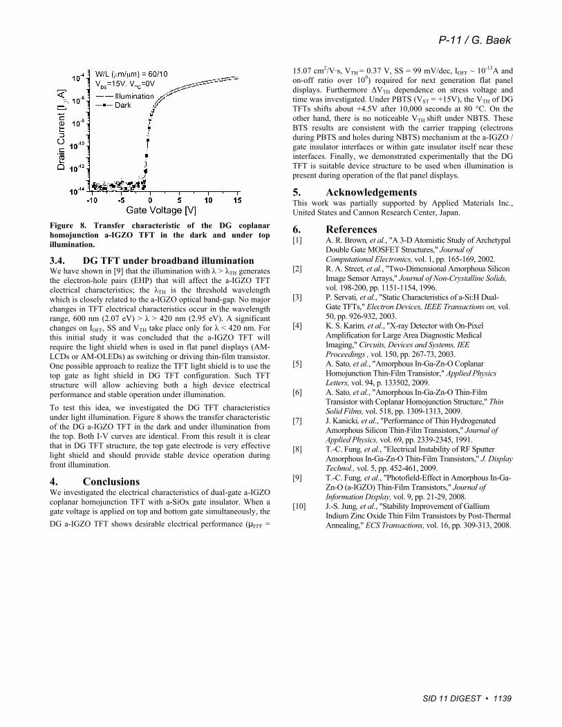
Figure 8. Transfer characteristic of the DG coplanar homojunction a-IGZO TFT in the dark and under top illumination.
3.4. DG TFT under broadband illumination We have shown in [9] that the illumination with λ > λTH generates the electron-hole pairs (EHP) that will affect the a-IGZO TFT electrical characteristics; the λTH is the threshold wavelength which is closely related to the a-IGZO optical band-gap. No major changes in TFT electrical characteristics occur in the wavelength range, 600 nm (2.07 eV) > λ > 420 nm (2.95 eV). A significant changes on IOFF, SS and VTH take place only for λ < 420 nm. For this initial study it was concluded that the a-IGZO TFT will require the light shield when is used in flat panel displays (AM-LCDs or AM-OLEDs) as switching or driving thin-film transistor. One possible approach to realize the TFT light shield is to use the top gate as light shield in DG TFT configuration. Such TFT structure will allow achieving both a high device electrical performance and stable operation under illumination.
To test this idea, we investigated the DG TFT characteristics under light illumination. Figure 8 shows the transfer characteristic of the DG a-IGZO TFT in the dark and under illumination from the top. Both I-V curves are identical. From this result it is clear that in DG TFT structure, the top gate electrode is very effective light shield and should provide stable device operation during front illumination.
4. Conclusions We investigated the electrical characteristics of dual-gate a-IGZO coplanar homojunction TFT with a-SiOx gate insulator. When a gate voltage is applied on top and bottom gate simultaneously, the
DG a-IGZO TFT shows desirable electrical performance (μEFF =
15.07 cm2/V·s, VTH = 0.37 V, SS = 99 mV/dec, IOFF ~ 10-13A and on-off ratio over 109) required for next generation flat panel displays. Furthermore ΔVTH dependence on stress voltage and time was investigated. Under PBTS (VST = +15V), the VTH of DG TFTs shifts about +4.5V after 10,000 seconds at 80 °C. On the other hand, there is no noticeable VTH shift under NBTS. These BTS results are consistent with the carrier trapping (electrons during PBTS and holes during NBTS) mechanism at the a-IGZO / gate insulator interfaces or within gate insulator itself near these interfaces. Finally, we demonstrated experimentally that the DG TFT is suitable device structure to be used when illumination is present during operation of the flat panel displays.
5. Acknowledgements This work was partially supported by Applied Materials Inc., United States and Cannon Research Center, Japan.
6. References [1] A. R. Brown, et al., "A 3-D Atomistic Study of Archetypal
Double Gate MOSFET Structures," Journal of Computational Electronics, vol. 1, pp. 165-169, 2002.
[2] R. A. Street, et al., "Two-Dimensional Amorphous Silicon Image Sensor Arrays," Journal of Non-Crystalline Solids, vol. 198-200, pp. 1151-1154, 1996.
[3] P. Servati, et al., "Static Characteristics of a-Si:H Dual-Gate TFTs," Electron Devices, IEEE Transactions on, vol. 50, pp. 926-932, 2003.
[4] K. S. Karim, et al., "X-ray Detector with On-Pixel Amplification for Large Area Diagnostic Medical Imaging," Circuits, Devices and Systems, IEE Proceedings , vol. 150, pp. 267-73, 2003.
[5] A. Sato, et al., "Amorphous In-Ga-Zn-O Coplanar Homojunction Thin-Film Transistor," Applied Physics Letters, vol. 94, p. 133502, 2009.
[6] A. Sato, et al., "Amorphous In-Ga-Zn-O Thin-Film Transistor with Coplanar Homojunction Structure," Thin Solid Films, vol. 518, pp. 1309-1313, 2009.
[7] J. Kanicki, et al., "Performance of Thin Hydrogenated Amorphous Silicon Thin-Film Transistors," Journal of Applied Physics, vol. 69, pp. 2339-2345, 1991.
[8] T.-C. Fung, et al., "Electrical Instability of RF Sputter Amorphous In-Ga-Zn-O Thin-Film Transistors," J. Display Technol., vol. 5, pp. 452-461, 2009.
[9] T.-C. Fung, et al., "Photofield-Effect in Amorphous In-Ga-Zn-O (a-IGZO) Thin-Film Transistors," Journal of Information Display, vol. 9, pp. 21-29, 2008.
[10] J.-S. Jung, et al., "Stability Improvement of Gallium Indium Zinc Oxide Thin Film Transistors by Post-Thermal Annealing," ECS Transactions, vol. 16, pp. 309-313, 2008.
P-11 / G. Baek
SID 11 DIGEST • 1139