Embed Size (px)
Citation preview
Meier 208/MAPLD 20041
DMA Controller fora Credit-Card Size
Satellite Onboard ComputerMichael Meier, Tanya Vladimirova*, Tim Plant
and Alex da Silva Curiel
Surrey Satellite Technology Ltd. and*Surrey Space Centre
University of Surrey, Guildford, Surrey, UK
Meier 208/MAPLD 20042
Introduction
• The Surrey Space Centre has a long-term research programme called “ChipSat”. Its aim is to design a credit-card-size satellite, which weighs less than 100 g.
• The first step of this development is the miniaturisation of the satellite on-board data handling system (OBDH) using a System-on-a-Chip (SoC) implemented on a high-density FPGA.
• The SoC consists of a CPU and some other Intellectual Property (IP) cores as peripherals and supporting modules.
• An important IP core in the SoC On-Board Computer (OBC) is a Direct Memory Access Controller (DMAC).
• The aim of this project was the development of a suitable DMA controller for such a SoC.
Meier 208/MAPLD 20043
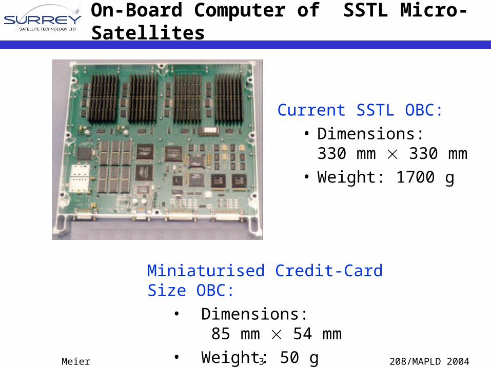
Current SSTL OBC:• Dimensions:
330 mm 330 mm• Weight: 1700 g
On-Board Computer of SSTL Micro-Satellites
Miniaturised Credit-Card Size OBC:• Dimensions: 85 mm 54 mm• Weight: 50 g
Meier 208/MAPLD 20044
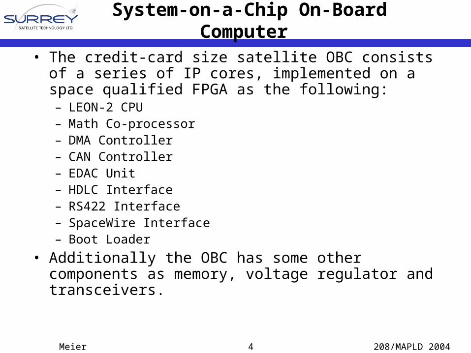
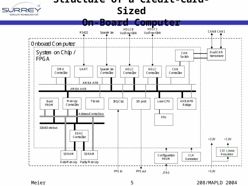
System-on-a-Chip On-Board Computer
• The credit-card size satellite OBC consists of a series of IP cores, implemented on a space qualified FPGA as the following:– LEON-2 CPU– Math Co-processor– DMA Controller– CAN Controller– EDAC Unit– HDLC Interface – RS422 Interface– SpaceWire Interface– Boot Loader
• Additionally the OBC has some other components as memory, voltage regulator and transceivers.
Meier 208/MAPLD 20045
Structure of a Credit-Card-SizedOn-Board Computer
Onboard Computer System on Chip / FPGA
Memory Controller
Timers IRQCtrl
UART DMA Controller
AHB/APB Bridge
AMBA AHB
32bit Data bus
Data Memory Parity Memory
CAN Controller
HDLC Controller
SpaceWire Controller
AMBA APB
FPU
HDLC Controller
CAN Switch
Leon CPU
EDAC Controller
Boot PROM
SDRAM SDRAM
Address/Control bus
RS422 SpaceWire HDLC1
Up/Downlink HDLC0
Up/Downlink CAN0 CAN1
Dual CAN transceiver
1.5V Linear Regulator
+3.3V
+3.3V +1.5V
CLK Generator
Configuration PROM
JTAG
I/O port
PPS out PPS in
Meier 208/MAPLD 20046
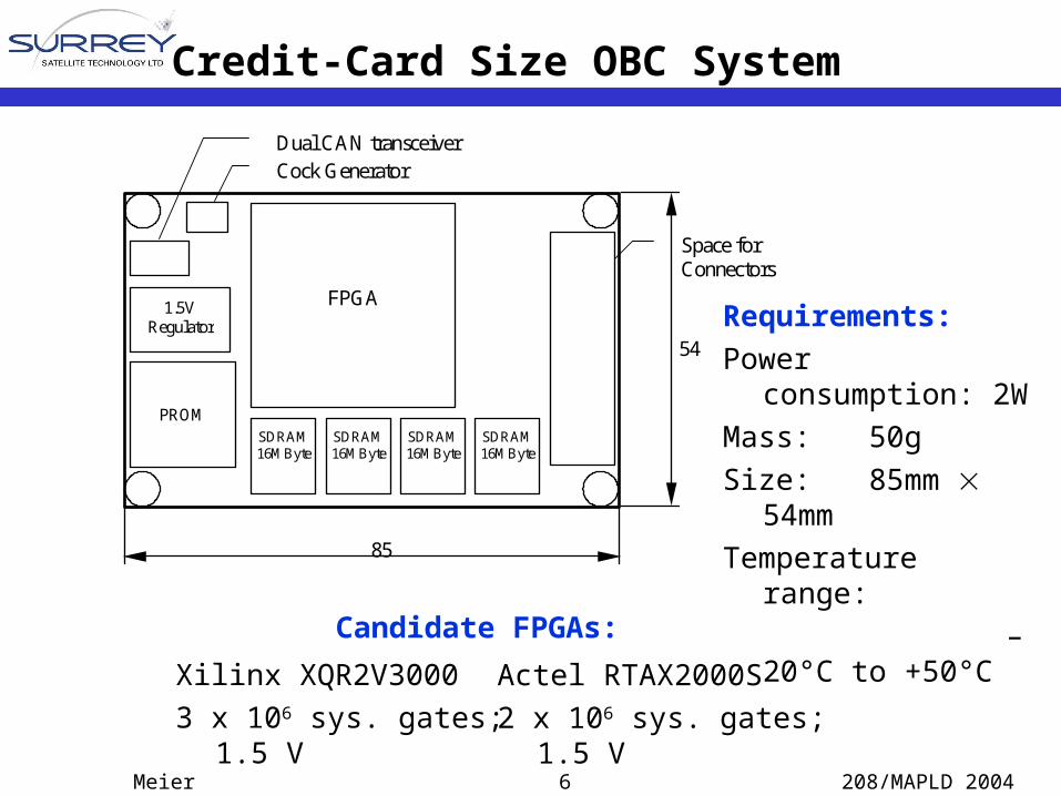
Credit-Card Size OBC System
Requirements:Power consumption: 2WMass: 50gSize: 85mm
54mmTemperature range: –20°C to +50°C
Xilinx XQR2V30003 x 106 sys. gates; 1.5 V
Actel RTAX2000S2 x 106 sys. gates; 1.5 V
Candidate FPGAs:
85
54
FPGA
Space for Connectors
1.5V Regulator
Cock Generator
PROM SDRAM 16MByte
Dual CAN transceiver
SDRAM 16MByte
SDRAM 16MByte
SDRAM 16MByte
Meier 208/MAPLD 20047
Purpose of a DMA Controller
• The credit-card size satellite OBC has several high data rate interfaces:– There is, for instance, a SpaceWire interface with a data rate up to
400 Mbit/s to connect to other devices. – Another interface is High Data Link Control (HDLC) with with up to
10 Mbit/s for up- and downlink to the ground station.
• All data sent or received must be transferred between the main memory and the interface controller at least with the data rate that the interface supports.
• The DMA controller handles these data transfers between the main memory and the interface controllers bypassing the CPU.
Meier 208/MAPLD 20048
Minimal System with a DMA Controller
RequestPeripheral
DeviceDMA
Controller
Memory
Acknowledge
CPU
On-Chip-BusInterrupt
BusArbiter
Meier 208/MAPLD 20049
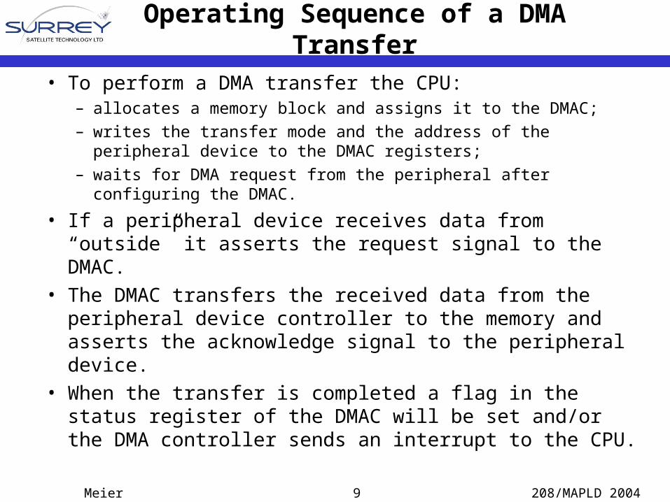
Operating Sequence of a DMA Transfer
• To perform a DMA transfer the CPU:– allocates a memory block and assigns it to the DMAC;– writes the transfer mode and the address of the peripheral device to the
DMAC registers; – waits for DMA request from the peripheral after configuring the
DMAC.
• If a peripheral device receives data from “outside” it asserts the request signal to the DMAC.
• The DMAC transfers the received data from the peripheral device controller to the memory and asserts the acknowledge signal to the peripheral device.
• When the transfer is completed a flag in the status register of the DMAC will be set and/or the DMA controller sends an interrupt to the CPU.
Meier 208/MAPLD 200410
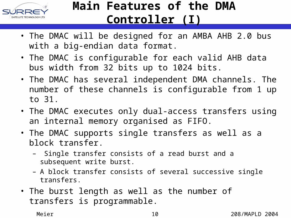
Main Features of the DMA Controller (I)
• The DMAC will be designed for an AMBA AHB 2.0 bus with a big-endian data format.
• The DMAC is configurable for each valid AHB data bus width from 32 bits up to 1024 bits.
• The DMAC has several independent DMA channels. The number of these channels is configurable from 1 up to 31.
• The DMAC executes only dual-access transfers using an internal memory organised as FIFO.
• The DMAC supports single transfers as well as a block transfer.– Single transfer consists of a read burst and a subsequent write burst. – A block transfer consists of several successive single transfers.
• The burst length as well as the number of transfers is programmable.
Meier 208/MAPLD 200411
Main Features of the DMA Controller (II)
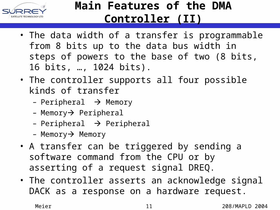
• The data width of a transfer is programmable from 8 bits up to the data bus width in steps of powers to the base of two (8 bits, 16 bits, …, 1024 bits).
• The controller supports all four possible kinds of transfer– Peripheral Memory– Memory Peripheral– Peripheral Peripheral– Memory Memory
• A transfer can be triggered by sending a software command from the CPU or by asserting of a request signal DREQ.
• The controller asserts an acknowledge signal DACK as a response on a hardware request.
Meier 208/MAPLD 200412
Main Features of the DMA Controller (III)
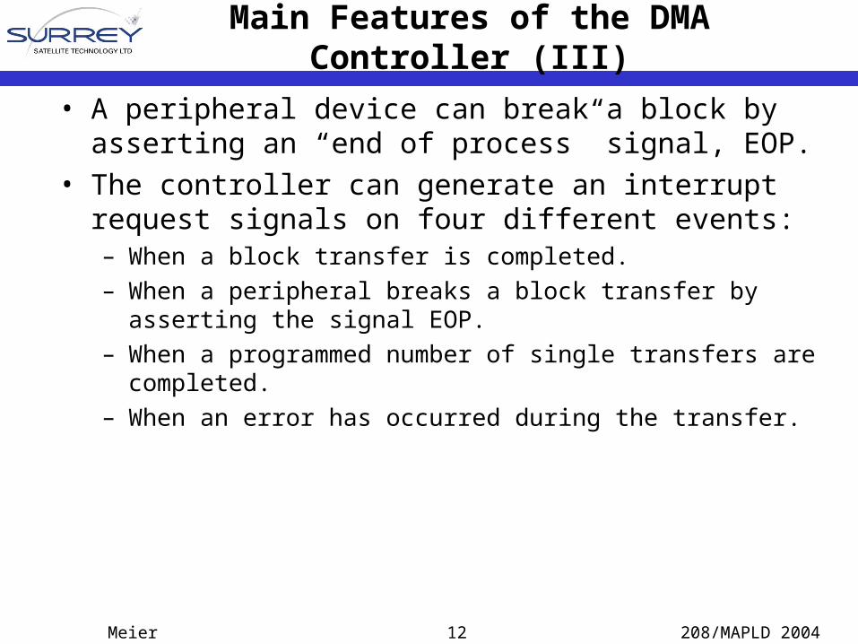
• A peripheral device can break a block by asserting an “end of process” signal, EOP.
• The controller can generate an interrupt request signals on four different events:– When a block transfer is completed.– When a peripheral breaks a block transfer by asserting the signal EOP.– When a programmed number of single transfers are completed.– When an error has occurred during the transfer.
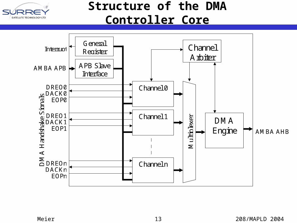
Meier 208/MAPLD 200413
Channel Arbiter
Channel 0 DACK0
EOP0
DREQ0
APB Slave Interface
General Register
Channel 1
Channel n
DACK1 EOP1
DREQ1
DACKn EOPn
DREQn
Mul
tiple
xer
AMBA AHB
DMA Engine
Interrupt
AMBA APB
DM
A H
ands
hake
Sig
nals
Structure of the DMA Controller Core
Meier 208/MAPLD 200414
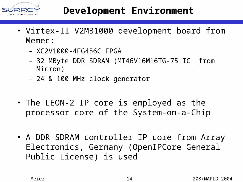
Development Environment
• Virtex-II V2MB1000 development board from Memec:– XC2V1000-4FG456C FPGA– 32 MByte DDR SDRAM (MT46V16M16TG-75 IC from Micron)– 24 & 100 MHz clock generator
• The LEON-2 IP core is employed as the processor core of the System-on-a-Chip
• A DDR SDRAM controller IP core from Array Electronics, Germany (OpenIPCore General Public License) is used
Meier 208/MAPLD 200415
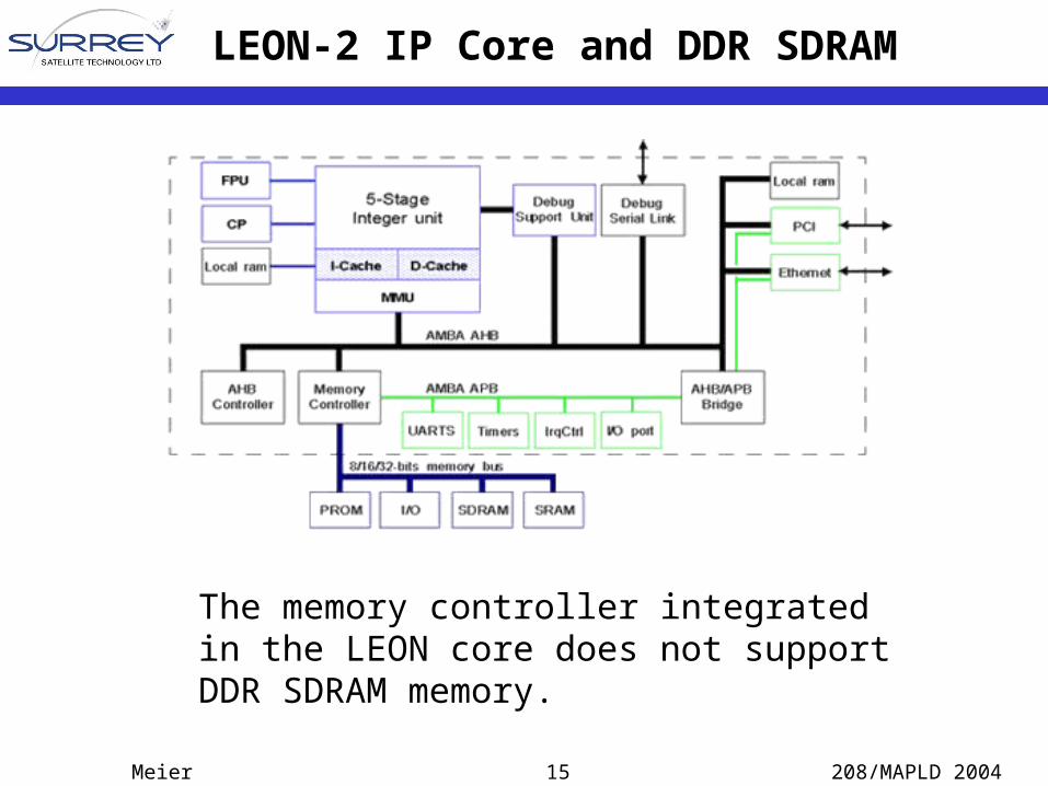
The memory controller integrated in the LEON core does not support DDR SDRAM memory.
LEON-2 IP Core and DDR SDRAM
Meier 208/MAPLD 200416
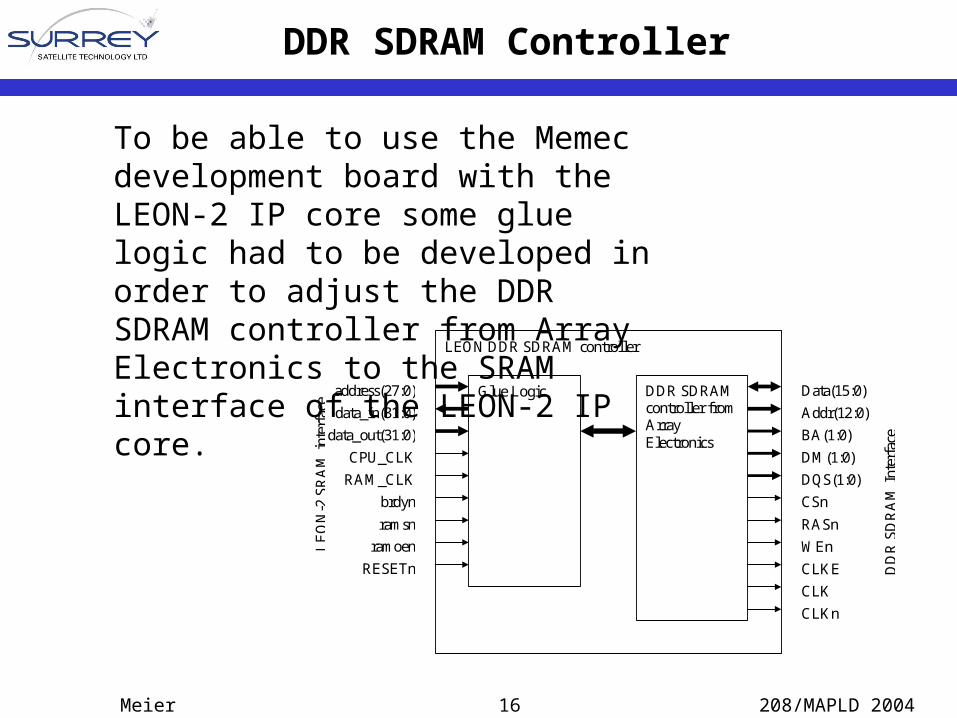
To be able to use the Memec development board with the LEON-2 IP core some glue logic had to be developed in order to adjust the DDR SDRAM controller from Array Electronics to the SRAM interface of the LEON-2 IP core.
DDR SDRAM Controller
LEON DDR SDRAM controller
Glue Logic DDR SDRAM controller from Array Electronics
Data(15:0) Addr(12:0) BA(1:0)
DQS(1:0) CSn RASn WEn CLKE CLK CLKn
DM(1:0)
RESETn
RAM_CLK CPU_CLK
brdyn
data_out(31:0) data_in(31:0) address(27:0)
ramsn ramoen LE
ON
-2 S
RA
M in
terf
ace
DD
R S
DR
AM
Inte
rfac
e
Meier 208/MAPLD 200417
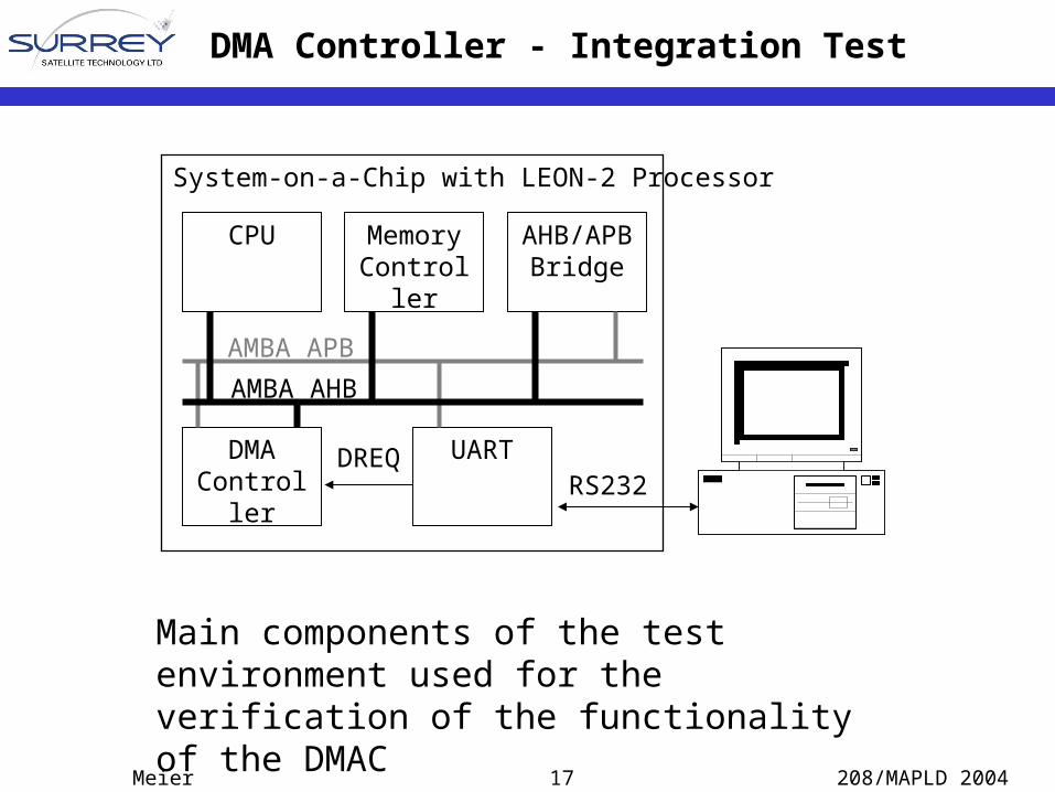
RS232
System-on-a-Chip with LEON-2 Processor
UARTDMA Controller
CPU
DREQ
AMBA AHB
Memory Controller
AHB/APB Bridge
AMBA APB
Main components of the test environment used for the verification of the functionality of the DMAC
DMA Controller - Integration Test
Meier 208/MAPLD 200418
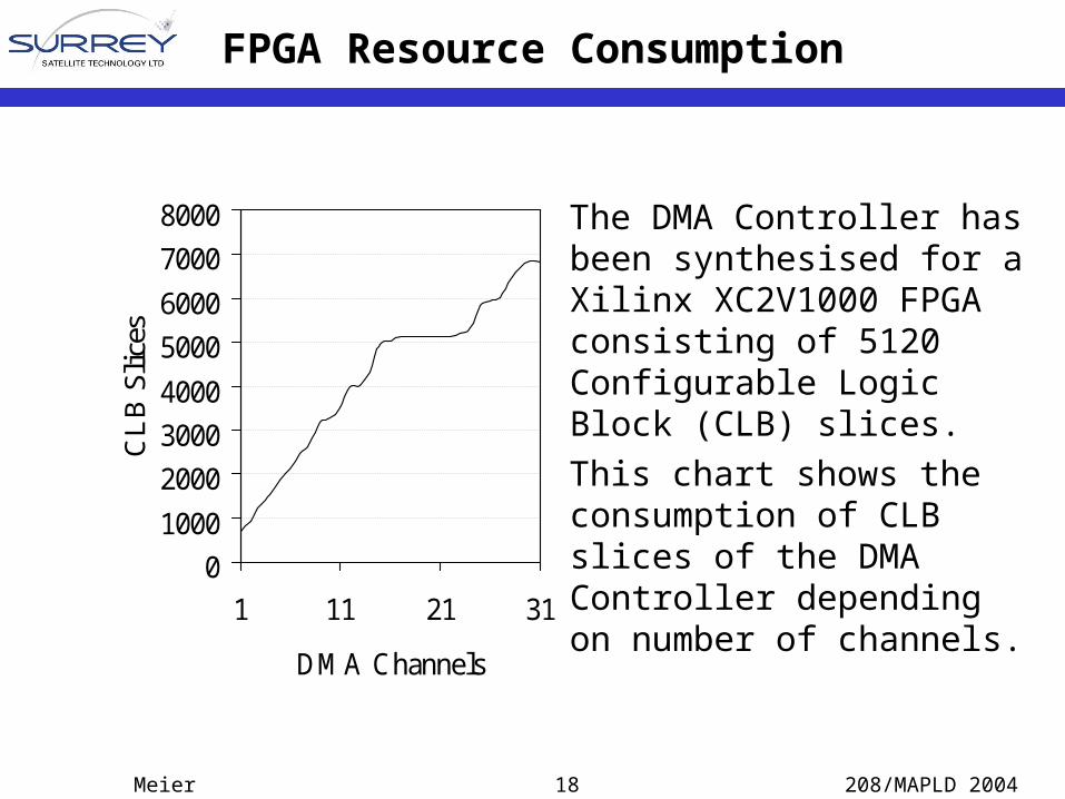
FPGA Resource Consumption
The DMA Controller has been synthesised for a Xilinx XC2V1000 FPGA consisting of 5120 Configurable Logic Block (CLB) slices.This chart shows the consumption of CLB slices of the DMA Controller depending on number of channels. 0
10002000300040005000600070008000
1 11 21 31
DMA Channels
CL
B S
lices
Meier 208/MAPLD 200419
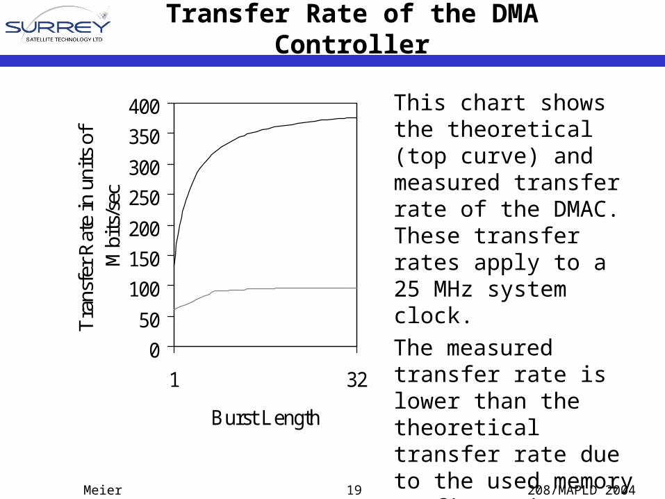
Transfer Rate of the DMA Controller
050
100150200250300350400
1 32
Burst Length
Tra
nsfe
r Rat
e in
uni
ts o
f M
bits
/sec
This chart shows the theoretical (top curve) and measured transfer rate of the DMAC. These transfer rates apply to a 25 MHz system clock. The measured transfer rate is lower than the theoretical transfer rate due to the used memory configuration.
Meier 208/MAPLD 200420
Conclusions
• A DMA controller specification for a SoC has been conceived supporting a list of typical and application-specific features.
• A sophisticated DMA controller has been designed.• The DMA controller has been implemented successfully as a
VHDL IP core.• The DMA Controller has been integrated together with the
LEON-2 IP core in a Xilinx Virtex-II FPGA. • The functionality of DMA controller has been tested
extensively.• The DMAC is suitable for use with High-bandwidth
Peripherals.• The following CAD tools have been used:
– Mentor ModelSim– Synplicity Synplify– XILINX Foundation ISE 5.1