Embed Size (px)
Citation preview

IEEE Santa Clara Valley Chapter, Components, Packaging and Manufacturing Technology Society
1/24/2013
www.cpmt.org/scv 1
Packaging for the Cloud Computing EraCloud Computing Era
Ilyas Mohammed
January 24, 2013
Contents
Cloud Computing
Cli t S
DIMM-in-a-Package/xFD
Design and
BVA PoP
F t
Conclusions
R dClient-Server
Trends
h ll
gPerformance
Assembly Results
l
Features
Assembly Process
Reliability
Roadmaps
Summary
2
Challenges Applications
xFD for DIMMs
Reliability Results

IEEE Santa Clara Valley Chapter, Components, Packaging and Manufacturing Technology Society
1/24/2013
www.cpmt.org/scv 2
Cloud Computing
Cli t S
DIMM-in-a-Package/xFD
Design and
BVA PoP
F t
Conclusions
R dClient-Server
Trends
h ll
gPerformance
Assembly Results
l
Features
Assembly Process
Reliability
Roadmaps
Summary
3
Challenges Applications
xFD for DIMMs
Reliability Results
Client: Mobile Devices as Digital Alter Ego
4
Mobile device is becoming the single one that does everything.
This requires high computing performance and wireless data at low power in small form factors.

IEEE Santa Clara Valley Chapter, Components, Packaging and Manufacturing Technology Society
1/24/2013
www.cpmt.org/scv 3
Wireless Network: Making Mobile Computing Possible
The classic client-server model“The network is the computer”
The current cloud computing model“The internet at hand”
5
High wireless bandwidth allows for full functionality and mobility
Wired networkFunctionally similar (difference largely in scale)Similar packaging (processors, memory, hard-drives, etc.)
Wireless networkFunctionally different (phones, tablets, laptops, servers)Different packaging (integrated vs. discrete)
Impact on Packaging
Pluggable componentsUpgradeableStandards driven
Integrated componentsNon-upgradeableClosed (vertically integrated)
Desktop computing Mobile computing
6
The trend towards integrated and closed systems has performance and design benefits.
This has tremendous impact on packaging including
o 3D chip packaging
o Modules and interposers
o Passives integration
o Connectors and sockets

IEEE Santa Clara Valley Chapter, Components, Packaging and Manufacturing Technology Society
1/24/2013
www.cpmt.org/scv 4
The Critical Interconnect
Data size & access hierarchyProcessing and access times
7
CPU-memory gap: it takes far longer to get data to the processor than it takes to use it
Processor-memory interface is the most critical one for computing performance
Processor-Memory Architecture
8
The interconnect determines the computing performance and power usage

IEEE Santa Clara Valley Chapter, Components, Packaging and Manufacturing Technology Society
1/24/2013
www.cpmt.org/scv 5
Cloud Computing
Cli t S
DIMM-in-a-Package/xFD
Design and
BVA PoP
F t
Conclusions
R dClient-Server
Trends
h ll
gPerformance
Assembly Results
l
Features
Assembly Process
Reliability
Roadmaps
Summary
9
Challenges Applications
xFD for DIMMs
Reliability Results
Miniaturization of a DIMM to a PackageSO-DIMM DIMM-in-a-Package
SO-DIMM DIMM-in-a-Package Advantage
67.6mm x 30mm x 3.8mm 22.5mm x 17.5mm x 1.2mm 81% area reduction
10
DIMM-in-a-Package is ideal for high performing mobile platforms
94% volume reduction
204 pins at 0.6 mm pitch 407 BGA at 0.8mm x 0.8mm pitch Twice the pins for better power/ground and IO options
Lower performance than a single package due to boards and
connectors
Same high performance as a single package due to BGA directly to
motherboard
DDR4/DDR5 Higher reliability

IEEE Santa Clara Valley Chapter, Components, Packaging and Manufacturing Technology Society
1/24/2013
www.cpmt.org/scv 6
FeaturesTop view Without mold
mo
ld)
Bottom view Without mold
Sid
e vi
ew (
wit
ho
ut
11
Functionally equivalent to a standard DIMM
4 chips in a single package (more chips possible)
Face-down wire-bond through windows for high performance
Front view (without mold)
Specifications
Quad-chip Face-Down Wire-bond BGA Package
407 BGA at 0.8mm x 0.8mm pitch
22.5mm x 17.5mm x 1.2mm package sizesize
Standard wire-bond CSP process
Single-step overmold including the windows
Pb-free 0.45mm solder ball diameter
12

IEEE Santa Clara Valley Chapter, Components, Packaging and Manufacturing Technology Society
1/24/2013
www.cpmt.org/scv 7
AssemblyWire-bondChip attach Mold and BGA attach
The first layer of chips are
13
attached, then a second layer of chips are attached (with a spacer if necessary), wire-bonded through the windows, molded, BGA attached and then marked and singulated.
Functional BGA Layout
A1 Corner 1 2 3 4 5 6 7 8 9 10 11 12 13 14 15 16 17 18 19 20 21 22 23 24 25 26 27
AA1
cornerVSS NC A0_i2c VDD_i2c DQ5 VSS DQ7 VDD VDD VDD ZQ NC VrefDQ NC VDD VDD VDD VSS DQ15 VSS DQ13 VSS VDDQ NC VSS
B VSS DQ4 VDDQ A1_i2c Eventb VDDQ VSS Reset DQSL DQ3 VSS DQ0 DML VrefCA DMH DQ8 VSS DQ11 DQSH VSS VSS VSS VDDQ VDDQ VSS DQ12 VSS
C DQ5 VDDQ DQ7 A2_i2c SCL DQ4 DQ6 VSS DQSLB VSS DQ2 DQ1 VSS VSS VSS DQ9 DQ10 VSS DQSHB VSS DQ14 DQ12 VDDQ VDDQ DQ15 VSS DQ13
D NC DQ6 VDDQ VSS SDA VDDQ VDDQ VSS VSS VSS VSS NC NC NC NC NC VSS VSS VSS VSS VSS VDDQ VDDQ VDDQ VDDQ DQ14 VSS
E DQ3 VSS VDDQ VSS VSS VSS VSS DQ11
F Reset DQSL DQSLB VSS VSS DQSHB DQSH ResetF Reset DQSL DQSLB VSS VSS DQSHB DQSH Reset
G VDD VSS VSS VDD VDD VSS VSS VDD
H VDD DQ0 DQ1 VDD A9 VDD A8 A1 A13 A11 VDD A11 A13 A1 A8 VDD A9 VDD DQ9 DQ8 VDD
J NC DQ2 VSS VDD BA0 A6 A7 VDD A0 CS1 NC CS3 A0 VDD A7 A6 BA0 VDD VSS DQ10 NC
K NC DML VDD NC A12 VSSCA A14 BA1 A2 A4 NC A4 A2 BA1 A14 VSSCA A12 NC VDD DMH NC
L VrefCA VrefDQ VSSCA NC NC CLK CLKB NC NC A3 VSSCA A3 CLKB CLK NC NC NC NC VSSCA VrefDQ VrefCA
M VSS VSS VDD NC CKE0 VSSCA BA2 CAS VSSCA RAS NC RAS VSSCA CAS BA2 VSSCA NC NC VDD VSS VSS
N ZQ DMH VSS VDD A10 A5 CKE1 VDD WE ODT1 NC ODT3 WE VDD NC A5 A10 VDD VSS DML ZQ
P VDD VSS DQ10 VDD ODT0 VDD A15 NC NC CS0 VDD CS2 CKE3 CKE2 A15 VDD ODT2 VDD DQ2 VSS VDD
R VDD DQ9 VSS VDD VDD VSS DQ1 VDD
T DQ8 VSS DQ11 VSS VSS DQ3 VSS DQ0
U VSS DQSH DQSHB VDDQ VDDQ DQSLB DQSL VSS
14
X64 data with two copies of address
Distributed power and ground design
A universal footprint supporting 2-8 DRAM devices of DDR, LPDDR and GDDR types
V NC DQ13 VDDQ VDDQ VDDQ VDDQ VSS VSS VSS VSS VSS NC NC NC NC NC VSS VSS VSS VSS VSS VDDQ VDDQ VDDQ VDDQ DQ5 NC
W DQ14 VDDQ VSS DQ12 VDDQ DQ15 VSS DQSHB VSS VSS DQ11 VSS DMH VSS DML VSS DQ3 VSS VSS DQSLB VSS DQ7 VDDQ DQ4 VSS VDDQ DQ6
Y VSS DQ15 DQ12 VSS DQ14 VSS VSS DQSH VDD DQ9 VSS VSS VSS VrefCA VSS VSS VSS DQ1 VDD DQSL VSS VSS DQ6 VDDQ DQ4 DQ7 VSS
AA VDDQ VDDQ DQ13 VSS VSS DQ10 VSS DQ8 VDD Reset ZQ NC VrefDQ NC VSS VDD VDD DQ0 VSS DQ2 VSS VSS DQ5 NC VDDQ

IEEE Santa Clara Valley Chapter, Components, Packaging and Manufacturing Technology Society
1/24/2013
www.cpmt.org/scv 8
Impact on PCB RoutingLow-profile laptop memory layout
DRAM routing DIMM-in-a-package routing
15
Routing individual memory devices requires HDI PCB
DIMM-in-a-Package has been specifically designed, including mirrored footprint for ease of routing when mounted on either side of the PCB. This allows for routing on a non-HDI PCB, reducing system costs significantly
Ultrabook Implementation
16
DIMM-in-a-Package successfully integrated within an ultrabook (the board was taken out to display the memory)
Highest performance (even more than DRAM packages on PCB) at lowest cost (significant board cost savings)

IEEE Santa Clara Valley Chapter, Components, Packaging and Manufacturing Technology Society
1/24/2013
www.cpmt.org/scv 9
Server Side Memory Challenge: Low Power Densification
Datacenters consume more than 120 GWh (~3% of total national electricity use)
Source: EPA report, 2007
17
( 3% of total national electricity use)
Memory is the biggest energy consuming component
Densification with high performance would significantly reduce power usage through lower losses and lower voltage, and more efficient thermal management
xFD Technology: High Performance Memory Densification
Conventional approaches
18
xFD offers face-down wire-bond interconnect for high performance for all the chips in the package (2, 3, or 4 are possible)
Conventional solutions suffer from asymmetric and low performance, besides being higher cost.
IEEE Santa Clara Valley Chapter, Components, Packaging and Manufacturing Technology Society
1/24/2013
www.cpmt.org/scv 10
High Performance in a Dense Package
Bottom chip Top chip
DQ
Data Eye Shmoo Plots at 2133 MT/s (15 unit sample size)Speed Bin Yield
DQ
DQS/ DQS#
19
Equal high performance from both top and bottom chips (95 0C, Advantest 5501)
There is >60% yield improvement at highest speed level compared to face-up stack
There is also a 25% reduction in chip junction temperature compared to face-up stack
DQS#
Bottom chip
Top chip
Face-up stack
DIMM Boards: High Performance with Easy RoutingControl/Address routing of quad-rank 16 GB LRDIMM using single layer only
20 2-chip xFD (DFD) solution easily beats even single chip solution
Module Tested Description One DIMM (4 DQ loads) Two DIMMs (8 DQ loads)
Invensas 8GB Quad-rank RDIMM
72 1Gb (x4) 1333MHz chips (36 DFD packages)
>1600MT/s 1600MT/s (with tuning)1333MT/s (no tuning)
Market 8GB Quad-rank RDIMM
36 2Gb (x8) 1333MHz chips (36 1-chip packages)
~1600MT/s 800MT/s (barely operates)

IEEE Santa Clara Valley Chapter, Components, Packaging and Manufacturing Technology Society
1/24/2013
www.cpmt.org/scv 11
Cloud Computing
Cli t S
DIMM-in-a-Package/xFD
Design and
BVA PoP
F t
Conclusions
R dClient-Server
Trends
h ll
gPerformance
Assembly Results
l
Features
Assembly Process
Reliability
Roadmaps
Summary
21
Challenges Applications
xFD for DIMMs
Reliability Results
Ultra High IO Between Processor and MemoryBGA PoP TMV PoP
2012 2013 2014 2015
IO 64 64 256 512
DDR data-rate (Mb )
800 1600 800 800(Mbps)
Bandwidth (GB/s) 6.4 12.8 25.6 51.2
Power Low High Low Low
22
Ultra-high IO interconnect technology is needed to achieve the high bandwidth desired between the CPU/GPU and memory Source: Samsung
IEEE Santa Clara Valley Chapter, Components, Packaging and Manufacturing Technology Society
1/24/2013
www.cpmt.org/scv 12
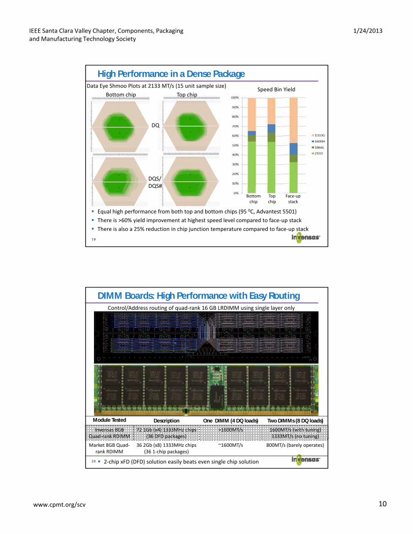
BVA PoP: FeaturesTop View Memory-Logic Interface
Side View
Bond Via Array (BVA)
23
Stand-off issue eliminated: Wire-bond based memory-logic interconnect
1000+ wide IO: 0.2 mm pitch easily possible
High performance at low-cost: Conventional PoP materials and processes
BVA PoP: Wide IO Support without TSV
2010 2011 2012 2013 2014 2015 2016?
Mobile DRAM LPDDR LPDDR2 LPDDR3Emerging
Wide IO Wide IO
Packaging PoP PoP PoP PoP BVA PoP TSV
Mobile processor to
168 168 240 240IO ranging from 200
1250memory interconnect
168 168 240 240g g
to 1000+1250
Clock Speed (MHz)
400 533 800High IO offers high bandwidth at low
speed200
Power 2X 1X 0.8XEnables intermediate
power reductions0.5X
# of Channels Single Single Dual Dual Quad+ Quad+
24
The goal of BVA PoP is to offer TSV capabilities for PoP applications utilizing conventional PoP infrastructure and materials.
Bandwidth (GB/s)
1.6 4.2 8.5 12.8 >12.8 >12.8

IEEE Santa Clara Valley Chapter, Components, Packaging and Manufacturing Technology Society
1/24/2013
www.cpmt.org/scv 13
BVA PoP: Specifications≥ 0.5 mm
≤ 1 mm
Very Fine Pitch Wire-Bond Interconnect
2 3 4 5 6
0.50 200 288 - - -
Assumptions:• Package size: 14 mm x 14 mm• IO edge to package edge: ≥ 0.5 mm• IO area width: ≤ 1 mm
mm
)
No. of IO rows
25
Assigning the same amount of area for IO as that of the current 0.5 mm pitch PoP, BVA with 0.2 mm pitch can offer up to 1440 IO.
0.50 200 288
0.40 248 360 - - -
0.30 336 492 640 - -
0.25 408 600 784 960 -
0.20 512 756 992 1220 1440
Pit
ch (
m
How to expose the ends of the wire-bonds cleanly within a given height over mold surface?
How to form free-standing wire-bonds whose end points are within tolerance (Δx, Δy, Δz)?
BVA PoP Challenges
How to reliably join the top and bottom packages at fine pitch with wire-bonds tips and solder?
There are 3 unique features that need to be demonstrated through assembly and testing.
Development engineering effort was carried out to determine the
26
carried out to determine the feasibility of this technology.
IEEE Santa Clara Valley Chapter, Components, Packaging and Manufacturing Technology Society
1/24/2013
www.cpmt.org/scv 14
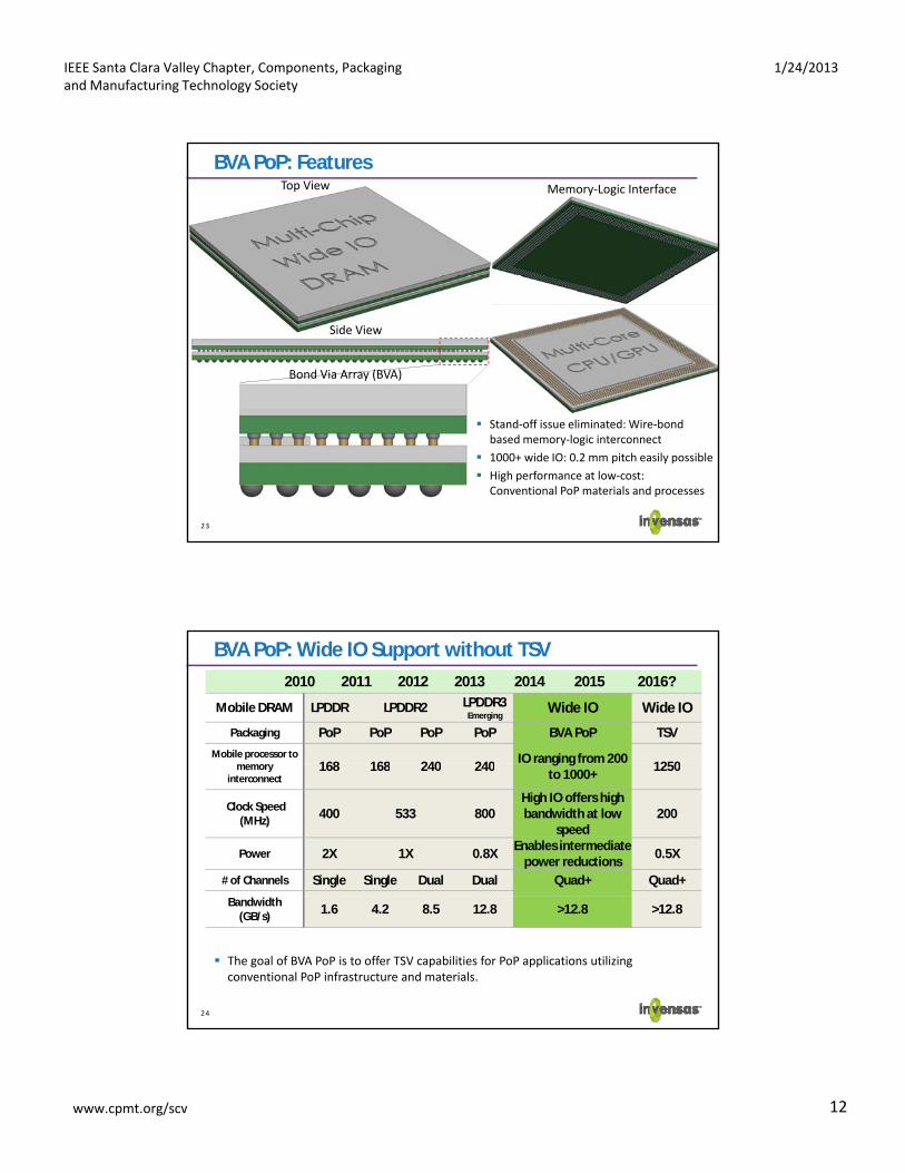
Test Vehicle Design
Package size 14 mm x 14 mm
Package thickness 1.36 mm
Bottom IO pitch 0.3 mm x 0.3 mm
Top IO pitch 0.24 mm x 0.24 mm
Number of IO rows 2
27
A 432 memory-logic interconnects were designed at 0.24 mm x 0.24 mm pitch to evaluate the feasibility of BVA technology.
Number of top IO 432
BVA PoP Process Flow
28
The 3 process steps unique to BVA PoP are highlighted and will be discussed in detail.

IEEE Santa Clara Valley Chapter, Components, Packaging and Manufacturing Technology Society
1/24/2013
www.cpmt.org/scv 15
Test Vehicle Assembly: Bottom Package
The flip-chip package is shown in strip form after wire-bonding BVA) and before overmolding.
29
The nominal height of the wire-bonds is 0.52 mm.
Test Vehicle Assembly: PoP Stack
Top surface of bottom package Fully Assembled BVA PoP Package
30
The top surface of the of the bottom package has bond wires projecting outwards by about 0.1 mm. The two packages were joined using conventional PoP SMT approach.

IEEE Santa Clara Valley Chapter, Components, Packaging and Manufacturing Technology Society
1/24/2013
www.cpmt.org/scv 16
Wire Bond Process—1/3
Wire spool control
Wire cut
Height Thermosonic, Ultrasonic
Bonding motion
Bond Capillary design
Wire shape control
Position
Bond Via Array (BVA) Process ParametersK&S ICONN Bonder
motion control
BVA Wire-bonds around the flip-chip die
31
The wire-bond height, position and bond quality depend on the process parameters as listed.
Wire Bond Process—2/3X-Position Y-Position Z-Position
Each data-point on graph represents a BVA package, h d ll h f d
OGP Position Measurement System
32
with average and range across all the free-standing wire-bonds.
The positional tolerance is acceptable (within ± 10 µm).
The range (the maximum difference between any two wire-bonds in a package) is high, and is being addressed through different techniques.
IEEE Santa Clara Valley Chapter, Components, Packaging and Manufacturing Technology Society
1/24/2013
www.cpmt.org/scv 17
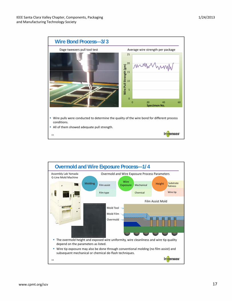
Wire Bond Process—3/3
Dage tweezers pull tool test Average wire strength per package
33
Wire pulls were conducted to determine the quality of the wire bond for different process conditions.
All of them showed adequate pull strength.
Overmold and Wire Exposure Process—1/4Assembly Lab Yamada G-Line Mold Machine
Overmold and Wire Exposure Process Parameters
Film assist
Film type
MoldingMechanical
Chemical
Wire Exposure
Substrate flatness
Wire tip
Height
Mold Tool
Mold Film
Overmold
Film Assist Mold
34
The overmold height and exposed wire uniformity, wire cleanliness and wire tip quality depend on the parameters as listed.
Wire tip exposure may also be done through conventional molding (no film assist) and subsequent mechanical or chemical de-flash techniques.
IEEE Santa Clara Valley Chapter, Components, Packaging and Manufacturing Technology Society
1/24/2013
www.cpmt.org/scv 18
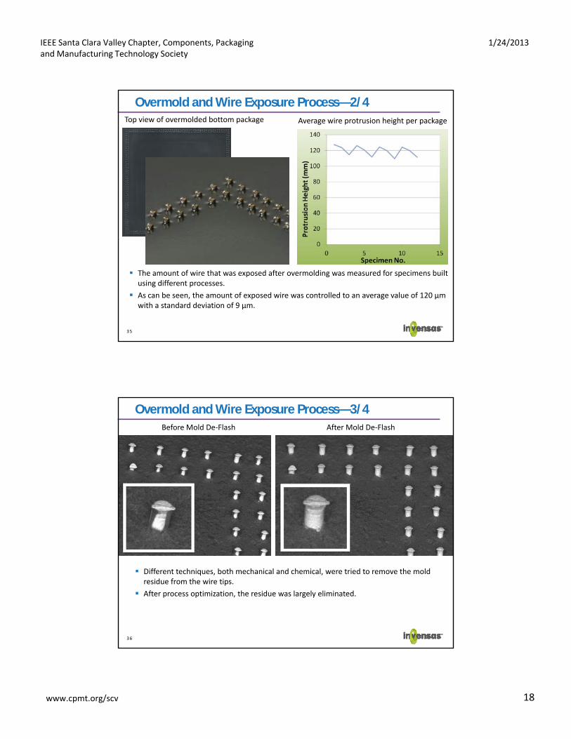
Overmold and Wire Exposure Process—2/4
Average wire protrusion height per package Top view of overmolded bottom package
35
The amount of wire that was exposed after overmolding was measured for specimens built using different processes.
As can be seen, the amount of exposed wire was controlled to an average value of 120 µm with a standard deviation of 9 µm.
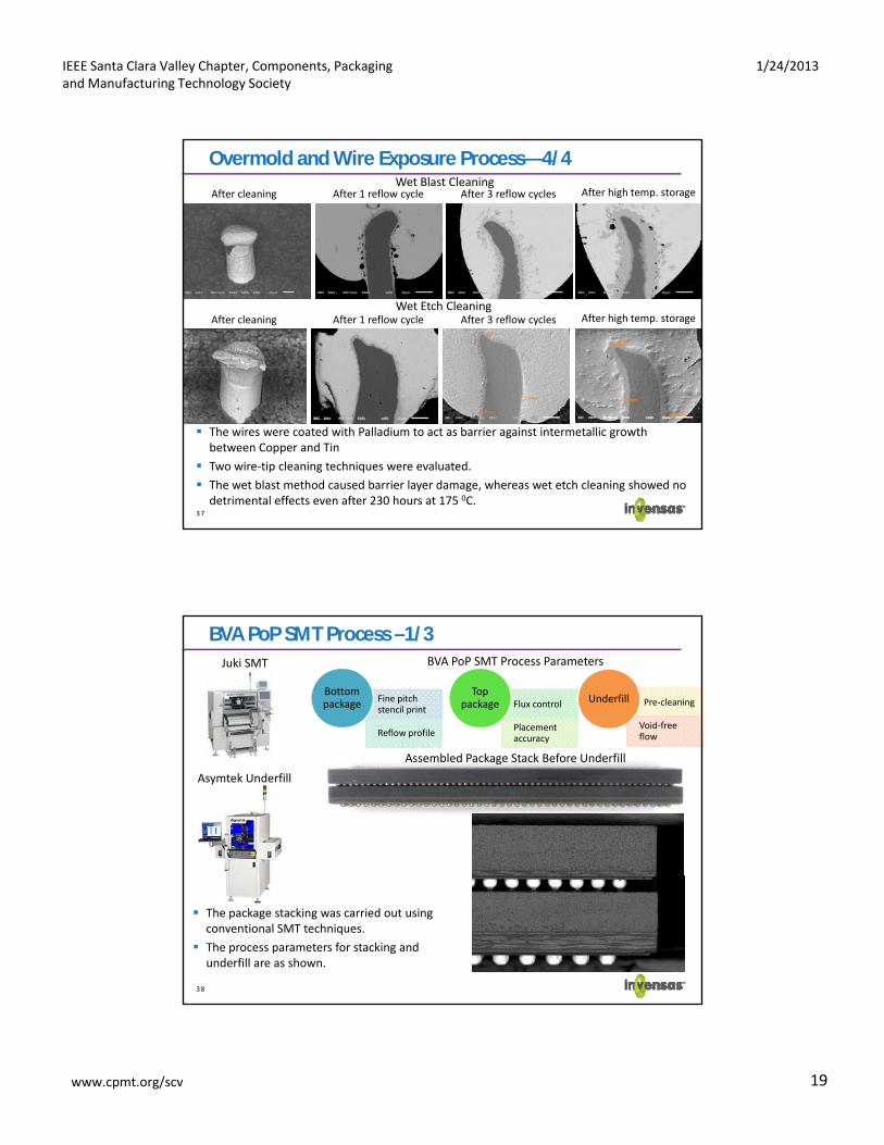
Overmold and Wire Exposure Process—3/4
Before Mold De-Flash After Mold De-Flash
36
Different techniques, both mechanical and chemical, were tried to remove the mold residue from the wire tips.
After process optimization, the residue was largely eliminated.
IEEE Santa Clara Valley Chapter, Components, Packaging and Manufacturing Technology Society
1/24/2013
www.cpmt.org/scv 19
Overmold and Wire Exposure Process—4/4Wet Blast Cleaning
After cleaning After 1 reflow cycle After 3 reflow cycles After high temp. storage
Wet Etch CleaningAfter cleaning After 1 reflow cycle After 3 reflow cycles After high temp. storage
37
The wires were coated with Palladium to act as barrier against intermetallic growth between Copper and Tin
Two wire-tip cleaning techniques were evaluated.
The wet blast method caused barrier layer damage, whereas wet etch cleaning showed no detrimental effects even after 230 hours at 175 0C.
BVA PoP SMT Process –1/3BVA PoP SMT Process Parameters
Fine pitch stencil print
Reflow profile
Bottom package Flux control
Placement accuracy
Top package Pre-cleaning
Void-free flow
Underfill
Juki SMT
Asymtek Underfill
Assembled Package Stack Before Underfill
38
The package stacking was carried out using conventional SMT techniques.
The process parameters for stacking and underfill are as shown.

IEEE Santa Clara Valley Chapter, Components, Packaging and Manufacturing Technology Society
1/24/2013
www.cpmt.org/scv 20
BVA PoP SMT Process –2/3Warpage at SAC Reflow Temperature (217 0C)
Top (memory) package Bottom (logic) package
Warpage: 42 µmWarpage: 48 µm
39
The warpage for both the packages at the reflow temperature was low enough to allow for package stacking with an IO pitch of 0.24 mm.
The presence of BVA protruding wires aid in overcoming the warpage issue through extra solder wetting surface of the post-like wire.
Warpage: 42 µm
BVA PoP SMT Process –3/3
40
One issue with SMT was non-uniform joints due to residue on one side of the wires . After de-flash, good joints were obtained.
The package stack SMT itself was uniform and consistent at a very fine pitch of 0.24 mm.
IEEE Santa Clara Valley Chapter, Components, Packaging and Manufacturing Technology Society
1/24/2013
www.cpmt.org/scv 21
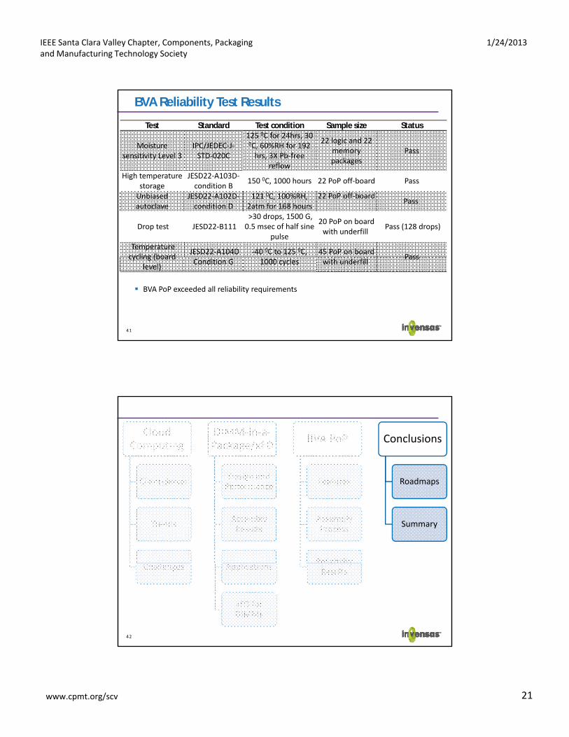
BVA Reliability Test Results
Test Standard Test condition Sample size Status
Moisture sensitivity Level 3
IPC/JEDEC-J-STD-020C
125 0C for 24hrs, 30 0C, 60%RH for 192
hrs, 3X Pb-free reflow
22 logic and 22 memory packages
Pass
Hi h JESD22 A103DHigh temperature storage
JESD22-A103D-condition B
150 0C, 1000 hours 22 PoP off-board Pass
Unbiased autoclave
JESD22-A102D-condition D
121 0C, 100%RH,2atm for 168 hours
22 PoP off-boardPass
Drop test JESD22-B111>30 drops, 1500 G,
0.5 msec of half sine pulse
20 PoP on board with underfill
Pass (128 drops)
Temperaturecycling (board
JESD22-A104D -40 0C to 125 0C, 45 PoP on board Pass
41
BVA PoP exceeded all reliability requirements
cycling (board level)
Condition G 1000 cycles with underfillPass
Cloud Computing
Cli t S
DIMM-in-a-Package/xFD
Design and
BVA PoP
F t
Conclusions
R dClient-Server
Trends
h ll
gPerformance
Assembly Results
l
Features
Assembly Process
Reliability
Roadmaps
Summary
42
Challenges Applications
xFD for DIMMs
Reliability Results

IEEE Santa Clara Valley Chapter, Components, Packaging and Manufacturing Technology Society
1/24/2013
www.cpmt.org/scv 22
Roadmaps: Invensas Memory Platform
b dd d
Client (DIMM-in-a-Package) Server (xFD, 2,3 & 4 chip package)
VLP RDIMM
SO-DIMM
Micro-DIMM
Tablets
Phones
Embedded
43
RDIMM
DIMM-in-a-Package is ideal for low profile space constrained mobile systems
xFD multi-chip package offers single-chip level high performance in a multi-chip configuration
Ultrabooks
Roadmaps: Invensas Mobile Platform
25.6BVA PoP: 500+ I/O0.25mm Pitch
BVA PoP: 1000+ I/O0.2mm Pitch
6 4
12.8
Me
mo
ry B
and
wid
th (G
B/s
)
µPILR PoP: 200+ I/O
µPILR PoP: 300-500 I/O0.3mm Pitch
44
A processor to memory bandwidth of up to 51.2 GB/s can be achieved through progression from BGA PoP (~6.4 GB/s) to µPILR PoP (6.4-12.8+ GB/s) and BVA PoP (25.6-51.2+ GB/s)
2010 2011 2012 2013 2014 2015
3.2
6.4 µPILR PoP: 200 I/O0.4mm Pitch
BGA PoP: <200 I/O0.5mm Pitch
IEEE Santa Clara Valley Chapter, Components, Packaging and Manufacturing Technology Society
1/24/2013
www.cpmt.org/scv 23
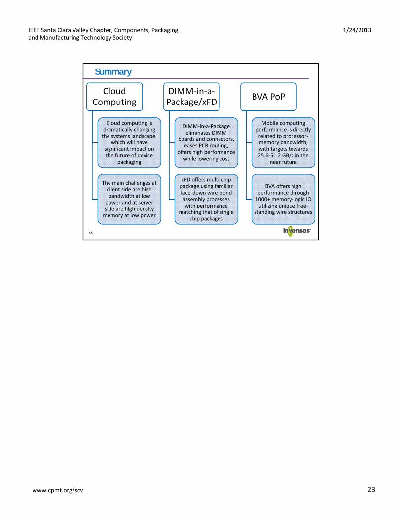
Summary
Cloud Computing
Cloud computing is
DIMM-in-a-Package/xFD
BVA PoP
Mobile computingCloud computing is dramatically changing
the systems landscape, which will have
significant impact on the future of device
packaging
h i h ll
DIMM-in-a-Package eliminates DIMM
boards and connectors, eases PCB routing,
offers high performance while lowering cost
xFD offers multi-chip
Mobile computing performance is directly related to processor-memory bandwidth, with targets towards 25.6-51.2 GB/s in the
near future
45
The main challenges at client side are high bandwidth at low
power and at server side are high density
memory at low power
xFD offers multi chip package using familiar face-down wire-bond assembly processes with performance
matching that of single chip packages
BVA offers high performance through
1000+ memory-logic IO utilizing unique free-
standing wire structures